3d metaphotonic nanostructures with intrinsic chiralityoptical chiral signals, even with a chiral...
TRANSCRIPT
REVIEWwww.afm-journal.de
© 2018 WILEY-VCH Verlag GmbH & Co. KGaA, Weinheim1803147 (1 of 16)
3D Metaphotonic Nanostructures with Intrinsic Chirality
Meng Qiu, Lei Zhang, Zhixiang Tang, Wei Jin, Cheng-Wei Qiu,* and Dang Yuan Lei*
Chirality is a universal geometric property in both micro- and macroworlds. Recently, optical chiral effects have drawn increased attention due to their great potential in fundamental studies and practical applications. Significantly, the optical chiral response of artificial structures can be enhanced by orders of magnitude compared to that of their naturally occurring counterparts. These man-made structures generally exhibit two types of optical chirality: extrinsic chirality and intrinsic chirality. The former relies on external illumination conditions, while the latter arises from the geometric characteristics of 3D objects. Herein, this review mainly focuses on the intrinsic chirality of artificial structures and discusses the existing realizations based on their design principles. In particular, an overview is given of the recent demonstrations of nonlinear optical effects in chiral structures and active chiral structures. Lastly, some promising prospects for future studies in the field are outlined.
DOI: 10.1002/adfm.201803147
plant leaves. Many daily items also utilize and benefit from chirality, including keys, staircases, and ropes. In fact, mirror sym-metry is much easier to be broken than to be maintained, and so it is more common for an object to be chiral. Chirality is important to fundamental physics because it is induced by symmetry-breaking. For example, chirality has become an impor-tant property of microparticles[1] after the proposition of nonconservation of parity.[2] Chirality was first noticed as an essential material property in modern science for the fact that organic molecules with dif-ferent chiralities possess distinct chemical behaviors. As the most essential organic molecules in living organisms, amino acids necessarily have chirality; they are composed of four different chemical groups and a carbon atom attached to
each of them, which is also the most explicit definition of chiral molecules. In living organisms, all 21 essential amino acids are L-enantiomers, indicating the high pressure of selecting chi-rality that results from life-maintaining chemical reactions.[3] The geometric structure of a molecule determines its optical chirality; however, it is very challenging to determine the geo-metric structures of molecules directly with current technolo-gies. Most molecules have different optical responses, such as refractive index and absorption, when illuminated by circularly polarized light (CPL) with different polarities. Therefore, the optical chiral response of molecules can be a promising indi-rect approach to distinguish their geometric information.
3D Metaphotonic Nanostructures
Dr. M. Qiu, Prof. W. JinDepartment of Electrical EngineeringThe Hong Kong Polytechnic UniversityHong Kong, ChinaProf. L. ZhangKey Laboratory for Physical Electronics and Devices of the Ministry of Education and Shaanxi Key Lab of Information Photonic TechniqueXi’an Jiaotong UniversityXi’an, Shaanxi 710049, ChinaProf. L. ZhangSchool of Electronic and Information EngineeringXi’an Jiaotong UniversityXi’an, Shaanxi 710049, ChinaProf. Z. TangCollege of Computer Science and Electronic EngineeringHunan UniversityChangsha 410082, China
1. Introduction
Chirality is a geometrical property of an object that can be found universally in macrostructures, such as human hands, and microstructures, such as molecules. A chiral object cannot be superposed onto its mirror image via either a translational or a rotational operation, or both. A chiral object and its mirror image are called enantiomorphs or, when referring to mol-ecules, enantiomers, which are often labeled as “left-handed” or “right-handed.” It has already been noticed that macroscopic chirality ubiquitously exists in various geometric structures, for instance, the rotation of seashells and the growth sequence of
Prof. C.-W. QiuDepartment of Electrical and Computer EngineeringNational University of Singapore4 Engineering Drive 3, Singapore 117583, SingaporeE-mail: [email protected]. C.-W. QiuNUS Suzhou Research Institute (NUSRI)Suzhou 215123, ChinaDr. D. Y. LeiDepartment of Applied PhysicsThe Hong Kong Polytechnic UniversityHong Kong, ChinaE-mail: [email protected]. D. Y. LeiShenzhen Research InstituteThe Hong Kong Polytechnic UniversityShenzhen 518057, China
The ORCID identification number(s) for the author(s) of this article can be found under https://doi.org/10.1002/adfm.201803147.
Adv. Funct. Mater. 2018, 28, 1803147

www.afm-journal.dewww.advancedsciencenews.com
1803147 (2 of 16) © 2018 WILEY-VCH Verlag GmbH & Co. KGaA, Weinheim
The outstanding properties of optical chiral materials mainly arise from the difference in their response to left circularly polar-ized (LCP) and right circularly polarized (RCP) light. When a lin-early polarized light passes through a chiral material, its plane of polarization rotates by a certain angle due to the difference in refractive index of LCP and RCP light. This effect is called optical rotation (OR) or circular birefringence (CB). On the other hand, the difference in the absorption of LCP and RCP light is usually called circular dichroism (CD).[4] OR and CD are basic represen-tations of optical chirality. By contrast, linear birefringence (LB) and linear dichroism (LD) are caused by the different refraction indices and absorption coefficients, respectively, of the two lin-early polarized waves with orthogonal directions and arise from the anisotropy of structures.[5,6] The response to both circularly and linearly polarized light could be a complementary technique to the elucidation of the structural information of biological or chemical molecules. However, when detecting the structures of molecules and nanostructures, LB and LD cannot be found in solutions where the directions of the molecules or nanostruc-tures are random, while OR and CD have no such requirement.
Recently, OR and CD measurements have been widely used to detect and analyze the structural, kinetic, and thermody-namic information of molecules, particularly the secondary structure and conformation of macromolecules.[7] However, the optical chiral response of most molecules is difficult to detect, which mainly results from their weak optical response, low concentration and random orientation in solution.
Optical chirality is not only generated by the quantum responses of molecules but also constructed by nanostructures. Further-more, particular nanostructures can give an optical chirality that is much stronger than that of molecules. This kind of special nano-structures can be found in living organisms. For example, gyroid nanostructures produce the vivid colors of butterfly wings,[8] and chiral microstructured patterns make jeweled beetles more bril-liant under LCP illumination than under RCP illumination.[9]
Recent studies on the optical responses of artificial nanostruc-tures, especially plasmonic metallic nanostructures, have pro-moted breakthroughs in the design of optical chiral materials. In a plasmonic system, the free electrons of metals can collectively oscillate at the dielectric/metal interface. When the charge oscil-lation is coupled with the incident electromagnetic radiation, the excited surface plasmon polaritons can propagate along the inter-face. On the other hand, when the charge oscillation occurs in a finite 3D nanostructure, it generates a standing wave and gives rise to a resonance called the localized surface plasmon resonance (LSPR). For both types of surface plasmons (SPs), the electro-magnetic field can be tightly confined along the direction normal to the structure surface and then can generate large near-field enhancement as well as a strong far-field optical response. Fur-thermore, such resonances are mainly determined by the motion patterns of the electrons inside. Various optical responses, such as perfect absorption[10,11] and phase modulation,[12] can be achieved with plasmonic nanostructures of different sizes, shapes and geometries. In addition, by virtue of the strong near-fields, the plasmon resonances of individual nanoparticles in a cluster can couple with each other and form collective modes based on their spatial arrangement. The plasmon hybridization theory was devel-oped to describe the coupling behaviors between LSPR modes and the generation of new plasmonic modes by considering the
hybridization of individual modes.[13] The past decade has wit-nessed a tremendous interest in such nanoclusters for the crea-tion of unusual optical properties and extended LSPR modes with new optical properties compared to isolated nanoparticles.[14]
Many theories have successfully described the optical chiral response of molecules. The simplest approach is to describe the chiral molecule by a single electron on a helix,[15,16] which can pre-dict the OR and CD responses of particular types of molecules. For more common cases, we can treat the optical response of one molecule or one part of the molecule as an oscillator and construct a coupled oscillator model,[17–22] which can describe the optical chirality of complex molecules. These theories have revealed that strict requirements are usually needed for generating strong
Meng Qiu finished his Ph.D. studies in theoretical physics in 2017 from Fudan University, China. He is cur-rently a research associate at the Hong Kong Polytechnic University. He has been doing nanophotonics research, including plasmonic mode coupling and chiral metas-tructures, since 2010.
Cheng-Wei Qiu received his Ph.D. degree in 2007, followed by a postdoctoral fellowship at the Physics Department of MIT until 2009. In December 2009, he joined NUS and was promoted to Associate Professor with tenure in January 2017. Since 1st Jan. 2018, he has been the Dean’s Chair in the Faculty of Engineering, NUS.
Dang Yuan Lei received his B.S., M.Phil., and Ph.D. degrees all in physics from Northwest University, Chinese University of Hong Kong, and Imperial College London in 2005, 2007, and 2011, respectively. He has been an assistant professor with the Department of Applied Physics at the Hong Kong Polytechnic University since
September 2012. His main research activities include nan-ophotonics and nanomaterials studies, with a particular interest in plasmon-enhanced light-matter interaction at the nanoscale and applications in energy harvesting, opto-electronic devices, and biophotonics.
Adv. Funct. Mater. 2018, 28, 1803147

www.afm-journal.dewww.advancedsciencenews.com
1803147 (3 of 16) © 2018 WILEY-VCH Verlag GmbH & Co. KGaA, Weinheim
optical chiral signals, even with a chiral geometry. In addition, it is difficult to change the geometry and molecular states of biochem-ical molecules. Fortunately, the development of metamaterials pro-vides a novel platform for designing optical chiral materials with strong and adjustable signals by shaping and arranging composite structures. Excitingly, artificial resonant modes such as LSPRs can be used to mimic the quantum oscillators in molecules, and the coupling between LSPRs can generate optical chirality that is enhanced by orders of magnitude in comparison with the counterparts of molecules. Mature fabrication methods, such as photolithography and electron-beam lithography (EBL), can easily realize planar structures with mirror symmetry along the normal direction of the sample surface, whereas it is difficult to realize 3D chiral nanostructures without mirror symmetry along any direction. An intuitive way to break this symmetry is to fabricate double-layer nanostructures. In addition, many other special methods have also been developed to fabricate 3D chiral nanostructures. As such, the chirality of molecules can also be enhanced by orders of magnitude using achiral nanostructures via a strong, localized near-field.[23–29] This effect is very useful in biomolecular sensing.[30,31]
Additionally, planar structures can also have an OR or CD response under an oblique illumination, which is called extrinsic chirality and is separate from intrinsic chirality—the chirality of 3D chiral structures.[32–34] To avoid the influence of extrinsic chi-rality, nanostructures are always formed as fourfold (C4) clusters, in which the extrinsic chirality of each structure would cancel that of the others and the only chiral signal would be that of intrinsic chirality.[35–39] We also do not need to consider extrinsic chirality when the nanostructures are in solution, for they are randomly distributed and there must be no anisotropy in the overall system. In this review, we only focus on intrinsic chirality generated by the 3D chiral structures, for it is more stable and universal, similar to the chirality of molecules.
This review article is organized as follows. We will first discuss the design principle of chiral nanostructures for producing optical chirality. We will then review relevant fabrication methods for real-izing chiral nanostructures and discuss the applications of chiral nanostructures, including second-harmonic generation (SHG), enhanced light–matter interaction and the use of active chiral materials. Finally, we will provide a conclusion and a brief perspec-tive on the future development of artificial chiral optical materials.
2. Design Principle of Optical Chiral Nanostructures
Geometric chirality and optical chirality are not equivalent to each other. Symmetry analysis can help to recognize geo-metric chirality but cannot predict optical chiral response. In fact, chiral structures do not necessarily have optical chiral response, either OR or CD, not to mention an enhanced chiral response. For an optical chiral medium, the constitutive relation can be expressed as[40–42]
0 r0
D Ei
cH
� � �ε ε χ= +
↔↔
(1)
and
Bi
cE H
00 r
� � �χ µ µ= − +↔
↔ (2)
where ε0, μ0, and c0 are the permittivity, permeability, and light
speed in vacuum, respectively; and rε↔
, rµ↔
, and χ↔
are the relative permittivity, permeability, and chirality tensors, respec-tively. It is obvious that a material with optical chiral response needs the electric and magnetic fields to be coupled to each other. To achieve nanostructures with an intense optical chiral response, we need to carefully investigate the following question from a fundamental principle level: what are the basic features of structures that support different responses to electric and mag-netic fields under LCP and RCP illumination? For simplicity, we consider the case that the material is isotropic, which means the parameters used in Equation (2) are scalars. Therefore, the refraction index and impedance can be expressed as[40–42]
r rn ε µ χ= ±± (3)
and
/0 r rz z µ ε=± (4)
where the + sign is for RCP, the—sign is for LCP, and z0 is the vacuum impedance. If we consider a chiral material with a thickness of d, the phase difference between the LCP and RCP waves is Re(n+ − n−)dk0, where k0 is the wave vector in vacuum. Thus, the OR can be expressed as θ = Re(χ)dk0. Similarly, we can express the transmittance as T± = exp[−Im(n+ − n−)k0d]. In case of a weak absorption, CD can be further simplified as CD ≈ 2k0dIm(χ).
Equation (3) suggests the possible realization of a negative refraction. When the chirality of the material is strong enough, i.e., Re(| | ) Re( )2
r r�χ ε µ , the material will present a negative refractive index for LCP or RCP light, which has been theo-retically proposed by Tretyakov et al.,[43] discussed by Pendry[44] and Monzon and Forester,[45] and experimentally verified in the microwave,[46–48] terahertz (THz),[49] and optical regions.[50,51]
Equations (2) and (4) give us a hint that a strong optical chiral response can be generated via the coupling between enhanced electric and magnetic responses.[32–35] Therefore, the question becomes how to generate an electric resonance and a magnetic resonance, which are exactly what artificial nanostructures can provide. By judiciously designing the geometric features of nanostructures, strong electric and magnetic fields can be generated through the strong localization of the EM field at a subwavelength space, which can mimic the oscillations of mole-cules. Therefore, those structures can be termed meta-atoms or meta-molecules. By contrast, the resonances of nanostructures can be manipulated artificially. Nevertheless, further demands need to be fulfilled. For example, split ring resonators, which are widely used building blocks for metamaterials, support both electric and magnetic resonances; however, no chirality takes place because of the orthogonality of the two resonances, which results in the absence of coupling. Therefore, coupling electric and magnetic resonances efficiently becomes a crucial requirement to generate optical chiral responses. To introduce a parallel component between the two resonances, helical metal structures were proposed by Engheta and Jaggard.[40] As shown in Figure 1a, a helical gold nanostructure with only one turn
Adv. Funct. Mater. 2018, 28, 1803147

www.afm-journal.dewww.advancedsciencenews.com
1803147 (4 of 16) © 2018 WILEY-VCH Verlag GmbH & Co. KGaA, Weinheim
supports two types of resonant modes when illuminated by CPL either parallel with or vertical to the axis of rotation. When the CPL is incident along the vertical direction of the axis, both electric and magnetic dipoles can be excited with well-aligned directions at its fundamental resonance of ≈1080 nm, as shown in the right panel of Figure 1a. Our simulation results (red line in Figure 1b) verify that a strong CD response can be observed at the resonances supported by the helical structure under this condition. We can see that the lowest three LSPRs are at 1080, 750, and 680 nm, with each exhibiting a CD peak.
Currently, it is still challenging to fabricate helical structures with rotary and out-of-plane features working in the visible range. Such a high requirement results from the relative direc-tion between a magnetic dipole and an electric dipole in the structures. In general, the directions of two types of dipoles tend to be vertical to each other, which lead to a negligible coupling between two modes. Alternatively, the magnetic dipole can be readily replaced by a specific electric dipole. When light is inci-dent along the z-axis, a magnetic dipole with a particular mag-netic conductivity in the x–y plane will have exactly the same response as an electric dipole with the same electric conductivity at a distance of λ/4 along the z-axis. This means that an electric resonator placed on a certain plane along the incident direc-tion (called an equiphase plane) is able to mimic a magnetic response at another equiphase plane. For example, as shown in Figure 1c, two orthogonal gold nanobars with a small separa-tion along the incident direction can mimic one electric and one magnetic dipole in the same direction. To obtain a strong optical chiral response, an efficient coupling between the two dipoles must be introduced through either a physical connection or a near-field interaction. Here, taking into consideration the electric field distribution of the dipole modes on the nanobars, we can control the coupling strength by varying their center-to-center separation, as shown in the inset of Figure 1d. Negligible CD is observed when two centers overlap, i.e., d = 0, which results from
zero-field at the center of the nanobar. By contrast, when the ends of the two bars are closer to each other, a strong coupling occurs, and the optical chiral response becomes enhanced. The underlying mechanism needs to be theoretically analyzed.[52,53]
In addition to shifting the relative positions of the two bars, we can also control their coupling strengths by varying orienta-tion, as shown in Figure 1e. Negligible CD is observed when two bars are orthogonal to each other, i.e., θ = 90°, which is the same as the case of d = 0 shown in Figure 1d. When the angle between the two bars decreases, a gradual increase in the overlap of the two near-fields will launch the coupling pro-cess and result in an increase in the CD signals, as shown in Figure 1f. Maximum CD signal occurs when θ = 45°. A further decrease in the relative angle will make the two bars more like the symmetric structures of a mirror. Then, the CD is reduced and vanishes when the two bars are parallel.
In particular, when incident light propagates along the rota-tional axis, the CD response at the second lowest resonance at ≈750 nm, shown in the left panel of Figure 1a, is stronger than that at the lowest resonance (≈1080 nm) or the third lowest resonance (≈680 nm), shown as the black line in Figure 1b. Inter-estingly, the resonances have opposite signs. Here, the mag-netic dipoles generated by the upper and lower parts of the helix cancel out each other, mostly due to their opposite current directions. By analyzing this mode, two coupled electric dipole resonators with different directions and in different equiphase planes were observed, similar to the case shown by Figure 1c,e. A similar explanation was also proposed by Gansel et al.[54] By com-paring the two cases in Figure 1b, we can further understand that optical chirality of one structure is not equivalent to geometric chirality and is also dependent on the excitation conditions.
In brief, previous realizations of strong optical chiral response were designed mainly based on the two principles as discussed above, i.e., the construction of nonorthogonally oriented electric and magnetic resonances or the positioning of two nonparallel
Adv. Funct. Mater. 2018, 28, 1803147
Figure 1. Typical optical chiral nanostructures and their CD spectra. a) The schematic of the electric and magnetic dipoles in a single helical nanopar-ticle at its lowest (right) and second lowest (left) resonances and b) their corresponding CD spectra when the incident wave is parallel (black line) or vertical (red line) to the axis of the helix. c) The schematic of two gold nanobars stacked orthogonally to each other and d) their simulated CD spectra when the centers of the bars are shifted by a distance of d. e) The schematic of two gold nanobars nonorthogonal to each other and f) their simulated CD spectra when the angle between the two nanobars is changed. In the FDTD simulations, periodic boundary conditions were used with a lattice constant of 400 nm. The system is illuminated by normal incidence, and the background is vacuum. All the nanostructures in the simulations are made of gold from the Palik database. The helix has a 60 × 100 nm2 cross-section and a diameter of 230 nm with a total length of 380 nm. The size of the gold nanobars is 60 × 60 × 300 nm3. The distance between the two nanobars along the direction of light is 200 nm.

www.afm-journal.dewww.advancedsciencenews.com
1803147 (5 of 16) © 2018 WILEY-VCH Verlag GmbH & Co. KGaA, Weinheim
electric resonances in different equiphase planes of incident light. The two types of resonant modes are then coupled with each other through a physical connection or near-field. Inter-estingly, the helical structure can match both design principles determined by the illumination conditions. Most optical chiral nanostructures can be categorized into these two cases, as we will demonstrate in the next part of this review. To construct complex structures, various nanofabrication technologies have been developed, including multistep lithography, direct laser writing (DLW), glancing angle deposition (GLAD), and self-assembly. However, it is not easy to realize 3D nanostructures matching the requirements discussed above. These methods will also be introduced in the next part of this review.
3. Realization of Optical Chiral Nanostructures
3.1. Chiral Nanostructures Realized by Electric–Magnetic Coupling
Following Equation (1)–(2), an optical chiral nanostructure is realized when it supports both electric and magnetic dipoles that are nonorthogonal to each other and can interact with inci-dent light efficiently. The original ideal was proposed by Eng-heta and Jaggard in 1988[40] and then realized in the microwave range, benefiting from the rapid development of metamaterials in the past ten years.[55–59] Several design models based on a twisted Ω-shaped particle are shown in Figure 2a,b.
Subsequently, various multilayer metallic structures with both electric and magnetic dipoles along the same direction have been designed;[55–60] however, most of them are too com-plicated to be fabricated at the micro- or nanoscale and are easier to be realized for THz waves due to the larger structure size.[49] As shown in Figure 2c–k, a rotated split ring was fab-ricated in a two-layer system. In the lower layer, a capacitor is formed by two rectangular patterns that act as two electrodes and support two electric dipoles vertical to the capacitor gap. A bridge, nearly parallel to the capacity gap, connects the two electrodes and supports a magnetic dipole moment along the bridge direction, as schematically shown in Figure 1d. Due to the small angle between the electric dipole and magnetic dipole, a strong coupling is anticipated. According to the standard effective media theory,[61,62] the calculated effective parameters can be used to express the mechanism of the optical chiral response. Zhao et al. have used this model to demonstrate the effective media of multiple kinds of chiral structures.[63]
3.2. Chiral Nanostructures Realized by the Direct Connection of Electric Dipoles
As “typical” chiral structures, helical structures intuitively match our understanding of chirality. Plasmonic nanohelical structures under normal illumination have been extensively studied by Gansel et al.[54] By using DLW, chiral holes were
Adv. Funct. Mater. 2018, 28, 1803147
Figure 2. Optical chiral nanostructures realized by the coupling of electric-magnetic resonances. a,b) The schematic of Ω-shaped particles. Repro-duced with permission.[59] Copyright 2010, the American Physical Society. c,d) The schematic of a vertical metallic chiral resonator and the direction of its electric and magnetic dipoles. e,f) SEM images of the experimental sample. g,h) The measured transmittance and transmission phases of the sample. i–k) The calculated effective permittivity, permeability and ξ. Reproduced with permission.[49] Copyright 2009, the American Physical Society.
www.afm-journal.dewww.advancedsciencenews.com
1803147 (6 of 16) © 2018 WILEY-VCH Verlag GmbH & Co. KGaA, Weinheim
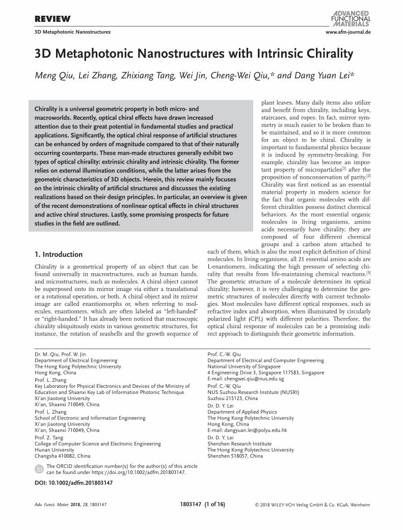
first generated in positive-tone photoresist on an indium tin oxide (ITO) glass substrate and then filled with gold via elec-trochemical deposition. After removing the resist, an elegant freestanding helical array was fabricated. Helical structures are able to generate a very broad optical chiral response due to the excitation of multiple resonant modes, as indicated by the simu-lated current distributions in Figure 3a. However, the role of each mode in generating optical chiral response differs. The lowest two modes contribute to the large transmission differ-ence under illumination with different handedness. With such a broad transmission stop band, the helical structure can be potentially applied as a circular polarizer. To further improve the extinction ratio and bandwidth, tapered helices have been developed, as shown in Figure 3b.[64] Furthermore, to eliminate
anisotropy, twisted nanohelices were proposed.[65–68] As shown in Figure 3c, a triple-helix structure was fabricated to main-tain rotational symmetry.[68] As given by Equation (4), isotropic chiral systems can realize an impedance match with the back-ground media. As a result, all of the optical chiral response should be ascribed to absorption. More importantly, these results further verified the physical understanding of the chirality of nanohelices under normal incidence. In twisted helices, the magnetic field does not contribute to the optical chiral response in the absence of the transverse component. Chirality must then arise from the coupling of misaligned electric dipoles in different equiphase planes of the incident light, which can effectively mimic a magnetic-like response. Another special helical structure was developed so that two helices with
Adv. Funct. Mater. 2018, 28, 1803147
Figure 3. Nanohelices and their optical chiral responses. a) The simulated transmittance and current distributions of gold nanohelices under the illumination of circularly polarized light. Reproduced with permission.[54] Copyright 2009, American Association for the Advancement of Science. b) SEM images of the tapered nanohelices. Reproduced with permission.[64] Copyright 2012, AIP Publishing LLC. c) SEM images of nanohelices with different geometric sizes. Reproduced with permission.[68] Copyright 2015, the Optical Society of America. d) SEM images of bichiral nanostruc-tures. Reproduced with permission.[70] Copyright 2011, Wiley-VCH. e) Measured and simulated CD of nanospirals with their SEM images and 3D models. Reproduced with permission.[71] Copyright 2013, Springer Nature Ltd. f) Freestanding metallic spirals fabricated by electron beam-induced deposition. Reproduced with permission.[72] Copyright 2015, American Chemical Society.
www.afm-journal.dewww.advancedsciencenews.com
1803147 (7 of 16) © 2018 WILEY-VCH Verlag GmbH & Co. KGaA, Weinheim
opposite chiralities were connected together.[69] When the upper helix is illuminated by one CPL, the current flows to the lower helix. Interestingly, the chirality of radiation is determined by the chirality of the lower helix, i.e., the opposite CPL. There-fore, this structure can work as a circular polarization con-verter. Radke et al. developed another technique to fabricate 3D bichiral structures by combining DLW and electroless silver plating, as shown in Figure 3d.[70] They first used two-photon femtosecond DLW in negative-tone photoresist to fabricate a 3D bichiral crystal. Then, the dielectric template was fully coated with a conformal silver film via electroless plating, which did not require an external current source. This method can be readily extended to fabricate extreme complex structures.
Other fabrication methods have also been used to create helices. GLAD was used to fabricate high-quality nanospi-rals.[73] Mark et al. have achieved two-pitched gold nanohelices with a strong optical chiral response of ≈700 nm.[71] The strong optical chiral response was ensured by the good quality of their structures, as indicated by the perfect matching between the simulated and experimental results shown in Figure 3e. Bai et al. followed this method and fabricated silver nanohel-ices with optical chiral responses at a shorter wavelength.[74] Electron beam-induced deposition has been used to produce nanospirals by Höflich et al.,[75] but the quality of fabrication is not well controlled. Recently, Esposito et al.[72,76,77] were able to fabricate nanospirals with remarkable qualities, which ensured a strong optical chiral response in the visible regime by mul-tiple LSPRs, as shown in Figure 3f.
Although helical structures have been demonstrated to be an effective medium to generate optical chiral response, high fabrication costs, and limited total fabrication areas make them ineligible for practical applications. In principle, high geometric chirality is not an indispensable component to achieve optical chiral response. In the following sections, we will introduce other works that have reported strong optical chiral responses without perfect helix structures. In particular, the released sample fabrication challenge will greatly broaden the applica-tions of artificial chiral structures.
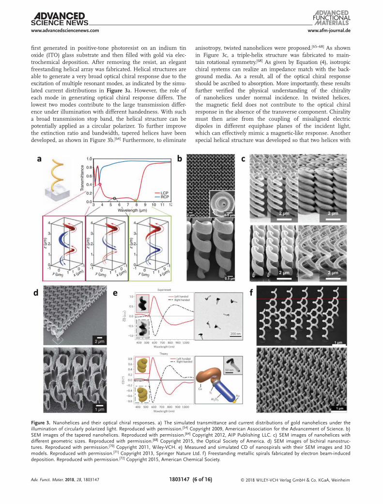
One of the major challenges is to realize freestanding hel-ical structures, since it is inevitable for there to be a small connection between the structures and the substrate for the consideration of mechanical stability and processing diffi-culty. If the rotation is less than one, the whole circular struc-ture can remain attached to substrate, which was achieved by Frank et al. using colloidal nanohole lithography, as shown in Figure 4a.[78] An intense optical chiral response was observed based on the hybridization of a series of LSPRs. By improving the fabrication technique for planar nanostructures, much effort has been made to fabricate 3D structures with a chiral response. It is intuitive to construct a nonplanar substrate, preventing the attached structures from the intrinsic mirror symmetry along the direction perpendicular to the plane. As shown in Figure 4b, for the first time, Dietrich et al. demon-strated a 3D L-shaped metallic strip with strong chirality via the excitation of complex LSPRs.[79] By applying similar designs, Dietrich et al. further fabricated star-shaped structures on a cone-shaped substrate and observed a high CD response.[80] Subsequently, many researchers have obtained structures with intense chirality through metallic strips on substrates with
particular structures.[81–84] In these studies, the substrate and/or the metal structure was fabricated using lithography. In particular, the relatively high precision demand calls for EBL for the fabrication of the nanostructures. However, one major drawback of this method is the limited fabrication area, usu-ally only up to the microscale. To solve the problem, Hou et al. applied self-assembled polystyrene nanospheres as the sub-strate and multistep GLAD to construct a metal top layer to achieve structures with both a strong optical chiral response and a large area, as shown in Figure 4c.[85,86]
Other studies have also successfully realized optical chirality within a single nanoparticle by implementing more compli-cated methods. For example, Helgert et al. applied multistep EBL to produce metal chiral nanostructures composed of two differently oriented L-shapes placed on different planes.[89] Cathcart and Kitaev have also obtained chiral nanostructures by a self-assembly approach.[90] Lee et al. grew gold nanopar-ticles in the environment of chiral molecules, and the chirality of the molecules was transferred to the nanoparticles.[87] Thus, they obtained two kinds of nanoparticles using molecules with opposite chiralities, as shown in Figure 4d.
The aforementioned chiral effects have been mainly achieved with single particles. Their optical chirality arises from the coupling electric dipoles disposed at different equiphase planes along the incident direction via direct connections. In addi-tion, there have also been other attempts to achieve single-par-ticle-based chirality. For example, starting with a 2D structure without planar symmetry, the mirror symmetry perpendicular to the plane can be destroyed using a metal substrate. Following such an idea, Karimullah et al. have created structures with strong optical chirality.[91] Zhu et al. have performed theoretical and experimental analyses of a 2D spiral structure on a metal film and compared them with those for 3D helical and 2D extrinsic chiral structures, as shown in Figure 4e.[88]
3.3. Chiral Nanostructures Realized by Near-Field Coupling of Electric Dipoles
As mentioned in Section 1 of this review, other than direct connection, near-field coupling is also an important method to couple two electric dipoles along different directions in dif-ferent equiphase planes of incident light. In this section, we will discuss chiral structures formed by two or more coupled nanoparticles. Although fabrication methods and different product forms are achieved, the basic mechanism of generating chirality is identical to those illustrated in Figure 1c–f.
Apart from lithography on nonplanar substrates introduced previously, multilayer of planar structures is also an important way to achieve 3D chiral structures. Generally, chiral nanostruc-tures fabricated by such methods are distinguished from two-layer coupled planar structures with different shapes. Due to the high feasibility of the multilayer method, the chirality of two-layer metal structures was first verified in the microwave regime.[46–48,92,93] By slightly breaking the symmetry in two layers with different sizes, Decker et al. observed a modest optical chiral response.[51] Afterward, Plum et al. produced a relatively stronger optical chirality through introducing a slightly rotating misalignment. A weak optical chirality was
Adv. Funct. Mater. 2018, 28, 1803147
www.afm-journal.dewww.advancedsciencenews.com
1803147 (8 of 16) © 2018 WILEY-VCH Verlag GmbH & Co. KGaA, Weinheim
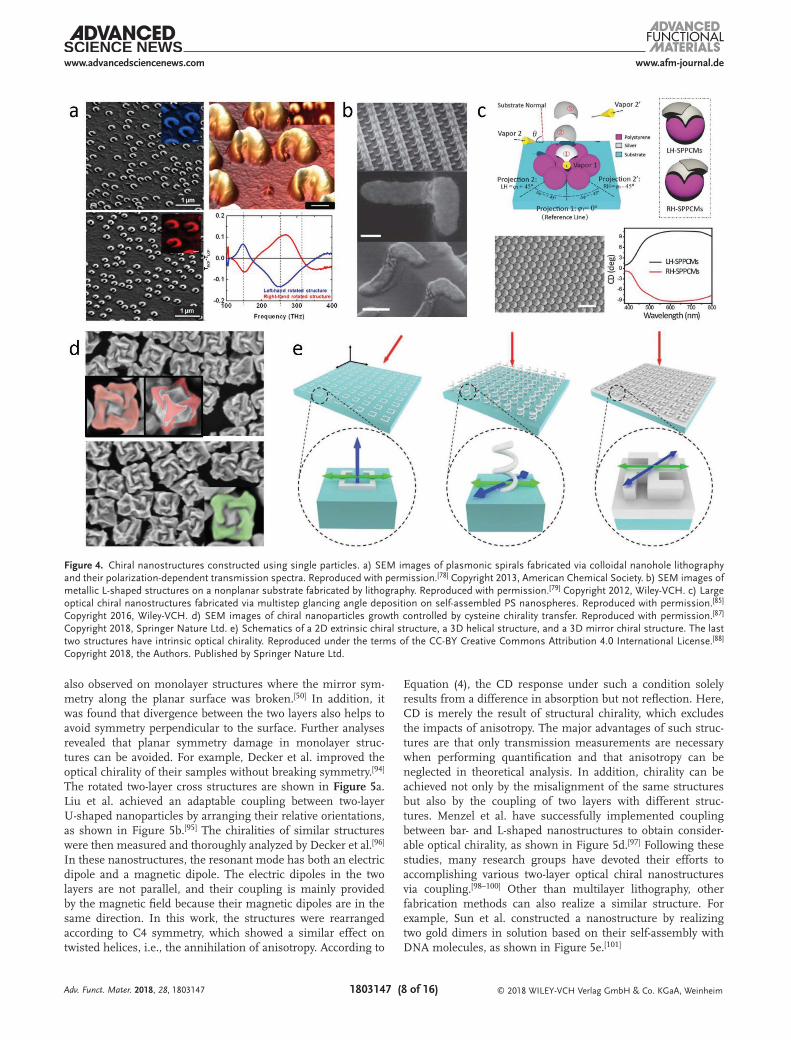
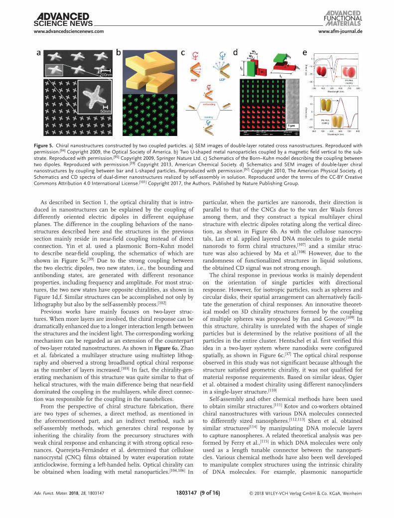
also observed on monolayer structures where the mirror sym-metry along the planar surface was broken.[50] In addition, it was found that divergence between the two layers also helps to avoid symmetry perpendicular to the surface. Further analyses revealed that planar symmetry damage in monolayer struc-tures can be avoided. For example, Decker et al. improved the optical chirality of their samples without breaking symmetry.[94] The rotated two-layer cross structures are shown in Figure 5a. Liu et al. achieved an adaptable coupling between two-layer U-shaped nanoparticles by arranging their relative orientations, as shown in Figure 5b.[95] The chiralities of similar structures were then measured and thoroughly analyzed by Decker et al.[96] In these nanostructures, the resonant mode has both an electric dipole and a magnetic dipole. The electric dipoles in the two layers are not parallel, and their coupling is mainly provided by the magnetic field because their magnetic dipoles are in the same direction. In this work, the structures were rearranged according to C4 symmetry, which showed a similar effect on twisted helices, i.e., the annihilation of anisotropy. According to
Equation (4), the CD response under such a condition solely results from a difference in absorption but not reflection. Here, CD is merely the result of structural chirality, which excludes the impacts of anisotropy. The major advantages of such struc-tures are that only transmission measurements are necessary when performing quantification and that anisotropy can be neglected in theoretical analysis. In addition, chirality can be achieved not only by the misalignment of the same structures but also by the coupling of two layers with different struc-tures. Menzel et al. have successfully implemented coupling between bar- and L-shaped nanostructures to obtain consider-able optical chirality, as shown in Figure 5d.[97] Following these studies, many research groups have devoted their efforts to accomplishing various two-layer optical chiral nanostructures via coupling.[98–100] Other than multilayer lithography, other fabrication methods can also realize a similar structure. For example, Sun et al. constructed a nanostructure by realizing two gold dimers in solution based on their self-assembly with DNA molecules, as shown in Figure 5e.[101]
Adv. Funct. Mater. 2018, 28, 1803147
Figure 4. Chiral nanostructures constructed using single particles. a) SEM images of plasmonic spirals fabricated via colloidal nanohole lithography and their polarization-dependent transmission spectra. Reproduced with permission.[78] Copyright 2013, American Chemical Society. b) SEM images of metallic L-shaped structures on a nonplanar substrate fabricated by lithography. Reproduced with permission.[79] Copyright 2012, Wiley-VCH. c) Large optical chiral nanostructures fabricated via multistep glancing angle deposition on self-assembled PS nanospheres. Reproduced with permission.[85] Copyright 2016, Wiley-VCH. d) SEM images of chiral nanoparticles growth controlled by cysteine chirality transfer. Reproduced with permission.[87] Copyright 2018, Springer Nature Ltd. e) Schematics of a 2D extrinsic chiral structure, a 3D helical structure, and a 3D mirror chiral structure. The last two structures have intrinsic optical chirality. Reproduced under the terms of the CC-BY Creative Commons Attribution 4.0 International License.[88] Copyright 2018, the Authors. Published by Springer Nature Ltd.
www.afm-journal.dewww.advancedsciencenews.com
1803147 (9 of 16) © 2018 WILEY-VCH Verlag GmbH & Co. KGaA, Weinheim
As described in Section 1, the optical chirality that is intro-duced in nanostructures can be explained by the coupling of differently oriented electric dipoles in different equiphase planes. The difference in the coupling behaviors of the nano-structures described here and the structures in the previous section mainly reside in near-field coupling instead of direct connection. Yin et al. used a plasmonic Born–Kuhn model to describe near-field coupling, the schematics of which are shown in Figure 5c.[39] Due to the strong coupling between the two electric dipoles, two new states, i.e., the bounding and antibonding states, are generated with different resonance properties, including frequency and amplitude. For most struc-tures, the two new states have opposite chiralities, as shown in Figure 1d,f. Similar structures can be accomplished not only by lithography but also by the self-assembly process.[102]
Previous works have mainly focuses on two-layer struc-tures. When more layers are involved, the chiral response can be dramatically enhanced due to a longer interaction length between the structures and the incident light. The corresponding working mechanism can be regarded as an extension of the counterpart of two-layer rotated nanostructures. As shown in Figure 6a, Zhao et al. fabricated a multilayer structure using multistep lithog-raphy and observed a strong broadband optical chiral response as the number of layers increased.[103] In fact, the chirality-gen-erating mechanism of this structure was quite similar to that of helical structures, with the main difference being that near-field dominated the coupling in the multilayers, while direct connec-tion was responsible for the coupling in the nanohelices.
From the perspective of chiral structure fabrication, there are two types of schemes, a direct method, as mentioned in the aforementioned part, and an indirect method, such as self-assembly methods, which generates chiral response by inheriting the chirality from the precursory structures with weak chiral response and enhancing it with strong optical reso-nances. Querejeta-Fernández et al. determined that cellulose nanocrystal (CNC) films obtained by water evaporation rotate anticlockwise, forming a left-handed helix. Optical chirality can be obtained when loading with metal nanoparticles.[104,106] In
particular, when the particles are nanorods, their direction is parallel to that of the CNCs due to the van der Waals forces among them, and they construct a typical multilayer chiral structure with electric dipoles rotating along the vertical direc-tion, as shown in Figure 6b. As with the cellulose nanocrys-tals, Lan et al. applied layered DNA molecules to guide metal nanorods to form chiral structures,[107] and a similar struc-ture was also achieved by Ma et al.[108] However, due to the randomness of functionalized structures in liquid solutions, the obtained CD signal was not strong enough.
The chiral response in previous works is mainly dependent on the orientation of single particles with directional response. However, for isotropic particles, such as spheres and circular disks, their spatial arrangement can alternatively facili-tate the generation of chiral responses. An innovative theoret-ical model on 3D chirality structures formed by the coupling of multiple spheres was proposed by Fan and Govorov.[109] In this structure, chirality is unrelated with the shapes of single particles but is determined by the relative positions of all the particles in the entire cluster. Hentschel et al. first verified this idea in a two-layer system where nanodisks were configured spatially, as shown in Figure 6c.[37] The optical chiral response observed in this study was not significant because although the structure satisfied geometric chirality, it was not qualified for material response requirements. Based on similar ideas, Ogier et al. obtained a modest chirality using different nanocylinders in a single-layer structure.[110]
Self-assembly and other chemical methods have been used to obtain similar structures.[111] Kotov and co-workers obtained chiral nanostructures with various DNA molecules connected to differently sized nanospheres.[112,113] Shen et al. obtained similar structures[114] by manipulating DNA molecule layers to capture nanospheres. A related theoretical analysis was per-formed by Ferry et al.,[115] in which DNA molecules were only used as a length tunable connector between the nanoparti-cles. Various chemical methods have also been well developed to manipulate complex structures using the intrinsic chirality of DNA molecules. For example, plasmonic nanoparticle
Adv. Funct. Mater. 2018, 28, 1803147
Figure 5. Chiral nanostructures constructed by two coupled particles. a) SEM images of double-layer rotated cross nanostructures. Reproduced with permission.[94] Copyright 2009, the Optical Society of America. b) Two U-shaped metal nanoparticles coupled by a magnetic field vertical to the sub-strate. Reproduced with permission.[95] Copyright 2009, Springer Nature Ltd. c) Schematics of the Born–Kuhn model describing the coupling between two dipoles. Reproduced with permission.[39] Copyright 2013, American Chemical Society. d) Schematics and SEM images of double-layer chiral nanostructures by coupling between bar and L-shaped particles. Reproduced with permission.[97] Copyright 2010, The American Physical Society. e) Schematics and CD spectra of dual-dimer nanostructures realized by self-assembly in solution. Reproduced under the terms of the CC-BY Creative Commons Attribution 4.0 International License.[101] Copyright 2017, the Authors. Published by Nature Publishing Group.

www.afm-journal.dewww.advancedsciencenews.com
1803147 (10 of 16) © 2018 WILEY-VCH Verlag GmbH & Co. KGaA, Weinheim
self-assembly induced by DNA molecules has become one of the most efficient ways to construct chiral clusters. By utilizing double helical DNA molecules, Song et al. obtained nanoclus-ters with a well-defined chiral arrangement, which was verified by the transmission electron microscopy (TEM) images and CD spectra shown in Figure 6d.[105] Similar techniques have also been implemented by other groups to realize structures with a strong optical chirality.[116–118] Interestingly, Shen et al. proposed a rolling-up method by decorating DNA origami with gold nan-oparticles to construct 3D plasmonic chiral nanostructures. A planar DNA layer, assembled with well-positioned gold nano-spheres, was rationally rolled to form a helical geometry.[119]
4. Applications of Optical Chiral Nanostructures
One of the most important applications of optical chiral nano-structures is to construct optical chiral devices, such as the pre-viously mentioned circular polarizer and complex optical field modulator. As introduced in Section 1, according to Equation (3), a negative index can also be obtained by chiral media. Chiral nanostructures actually possess many more prospective func-tions and thus show great potential for practical applications.
4.1. Second Harmonic Generation in Chiral Nanostructures
The intrinsic property of chiral nanostructures implies the total absence of mirror symmetry along any direction. In com-parison, SHG is only present when the structure has no inver-sion symmetry, which is a general principle for both molecules and artificial subwavelength structures. Rationally, chiral structures should possess strong SHG properties. Relative measurements suggest that the optical chiral effect of SHG is typically orders of magnitude larger than that of their linear counterparts.[120–123] The strong SHG signal of chiral struc-tures was first verified in planar designs. When an inclined incidence breaks the symmetry of the planar system, an optical chiral response similar to that of 3D chiral structures would then be generated.[33,124–126] Many groups have conducted SHG studies using the extrinsic chirality of planar structures. Sig-nificant SHG emission was observed in chiral structures, which can be called the SHG-CD effect.[127–130] Although the SHG-CD signals differs a lot under LCP and RCP excitations, there is a difference between extrinsic SHG-CD and extrinsic linear CD. When the sample is flipped around, the sign of its extrinsic CD signal would remain, while that of its extrinsic SHG-CD signal would change.[127]
Adv. Funct. Mater. 2018, 28, 1803147
Figure 6. Chiral nanostructures constructed by multiple coupled particles. a) Schematics and TEM images of multilayer chiral nanostructures fabri-cated by lithography. Reproduced with permission.[103] Copyright 2012, Springer Nature Ltd. b) Multilayer chiral nanostructures formed from cellulose nanocrystals self-assembled with gold nanorods. Reproduced with permission.[104] Copyright 2014, American Chemical Society. c) Chiral nanostructures formed by four nanoparticles based on two-layer lithography. Reproduced with permission.[37] Copyright 2012, American Chemical Society. d) Double helices formed by gold nanospheres. The arrangement of the spheres follows the chirality of the DNA molecules. Reproduced with permission.[105] Copyright 2013, American Chemical Society.
www.afm-journal.dewww.advancedsciencenews.com
1803147 (11 of 16) © 2018 WILEY-VCH Verlag GmbH & Co. KGaA, Weinheim
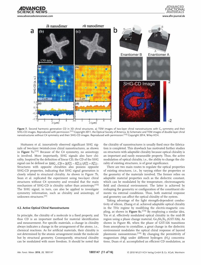
Huttunen et al. innovatively observed significant SHG sig-nals of two-layer twisted-cross chiral nanostructures, as shown in Figure 7a.[131] Because of the C4 symmetry, no anisotropy is involved. More importantly, SHG signals also have chi-rality. Inspired by the definition of linear CD, the CD of the SHG signal can be defined as SHG_ CD 2( )/( )LCP
2RCP2
LCP2
RCP2P P P P= − +ω ω ω ω .
Structures with opposite chiralities also possess opposite SHG-CD properties, indicating that SHG signal generation is closely related to structural chirality. As shown in Figure 7b, Sean et al. replicated the experiment using two-layer chiral structures without C4 symmetry and revealed that the main mechanism of SHG-CD is chirality rather than anisotropy.[132] The SHG signal, in turn, can also be applied to investigate symmetry information, such as chirality and anisotropy, of unknown structures.[41]
4.2. Active Optical Chiral Nanostructures
In principle, the chirality of a molecule is a fixed property, and thus CD is an important method for material identification and measurement. For specific materials, a change in chirality always indicates a change in the arrangement of the atoms, i.e., chemical reactions. As for artificial materials, their chirality is not determined by the atomic arrangement inside the molecule but by structural geometry. Consequently, structural chirality can be modulated with more freedom. It should be noted that
the chirality of nanostructures is usually fixed once the fabrica-tion is completed. This drawback has motivated further studies on structures with adaptable chirality because optical chirality is an important and easily measurable property. Thus, the active modulation of optical chirality, i.e., the ability to change the chi-rality of existing structures, is of great significance.
There are two main routes to regulate the optical properties of existing structures, i.e., by varying either the properties or the geometry of the materials involved. The former relies on adaptable material properties such as the dielectric constant, which can be modulated by the temperature, electromagnetic field and chemical environment. The latter is achieved by reshaping the geometry or configuration of the constituent ele-ments via external conditions. Thus, both material response and geometry can affect the optical chirality of the system.
Taking advantage of the light strength-dependent conduc-tivity of silicon, Zhang et al. achieved adaptable optical chirality in the THz regime by modifying the electric-magnetic cou-pling, as shown in Figure 8a.[133] By employing a similar idea, Yin et al. effectively modulated optical chirality in the mid-IR region using a phase change material, Ge3Sb2Te6 (GST-326). As shown in Figure 8b, when the phase of GST-326 transitions from amorphous to crystalline, a great change in the dielectric environment modulates the optical chiral response of layered plasmonic nanoantennas.[134] By changing the permittivity of magnesium (Mg) under different hydrogen (H2) concentra-tions, Duan et al. accomplished an efficient CD modulation, as
Adv. Funct. Mater. 2018, 28, 1803147
Figure 7. Second harmonic generation CD in 3D chiral structures. a) TEM images of two-layer chiral nanostructures with C4 symmetry and their SHG-CD images. Reproduced with permission.[131] Copyright 2011, the Optical Society of America. b) Schematic and TEM images of double-layer chiral nanostructures without C4 symmetry and their SHG-CD images. Reproduced with permission.[132] Copyright 2014, Wiley-VCH.

www.afm-journal.dewww.advancedsciencenews.com
1803147 (12 of 16) © 2018 WILEY-VCH Verlag GmbH & Co. KGaA, Weinheim
shown in Figure 8c.[135] It is noteworthy that the structures in all three works have C4 symmetry, which verifies that CD change is solely a consequence of alterations in structural chirality.
Since chirality is a geometric property, the alteration of geometry can efficiently modulate the structural optical chiral response. Thus, flexible materials are an excellent candidate for designing reconfigurable structures. Taking advantage of the modest hardness of gold, Kan et al. designed a structure with flexible gold spirals fabricated in microholes on a silicon sub-strate. The stretch directions of the gold spirals were controlled by barometric changes in the two flanking spaces. Opposite chi-rality observed under opposite stretch directions further proved that this nanostructure is indeed geometrically adaptable, as
shown in Figure 8d.[136] Limited by the elasticity of metal mate-rials, it is unfeasible for this structure to be reduced to the optical regime. A similar design was realized in the microwave regime by Slobozhanyuk et al. and was used to tune nonlinear responses.[139]
Schreiber et al. employed spherical nanoclusters assembled from DNA nanohelices as a chiral structure since the structural direction can be altered accordingly in a distributed environ-ment.[140] When placed in buffer, the DNA molecules of the structure become vertical to the surface. By contrast, when the buffer is removed and the surface dries up, the DNA nanohel-ices bend down into a parallel direction with the surface. The optical chiral responses are significantly different under these
Adv. Funct. Mater. 2018, 28, 1803147
Figure 8. Active 3D chiral structures. a) Schematic and SEM images of a two-layer active chiral structure. This structure can be tuned by extra light field to change the THz CD. Reproduced with permission.[133] Copyright 2012, Springer Nature Ltd. b) Thermally induced active chiral structure based on GST-326, whose material properties can also be electrically and optically switched. Reproduced with permission.[134] Copyright 2015, American Chem-ical Society. c) Hydrogen-regulated active chiral structure. Reproduced with permission.[135] Copyright 2016, American Chemical Society. d) Mechanically induced active chiral structure based on MEMS. Reproduced under the terms of the CC-BY Creative Commons Attribution 4.0 International License.[136] Copyright 2015, the Authors. Published by Springer Nature Ltd. e) DNA-regulated chiral nanostructure. Reproduced with permission.[137] Copyright 2014, Springer Nature Ltd. f) Chiral nanostructure with nanorods can actively “walk” on a DNA plane. Reproduced with permission.[138] Copyright 2015, American Chemical Society.
www.afm-journal.dewww.advancedsciencenews.com
1803147 (13 of 16) © 2018 WILEY-VCH Verlag GmbH & Co. KGaA, WeinheimAdv. Funct. Mater. 2018, 28, 1803147
two conditions, similar to the case shown in Figure 1b. Taking the reconfigurable DNA origami template consisting of two helical bundles as a prototype, Kuzyk et al. further attached a gold nanorod to each of the two helical bundles to achieve a chiral structure. Since the optical chiral response is dependent on the angle between the two helices and the helical angle is determined by the DNA molecules at their ends, the modula-tion of optical chiral responses can be achieved by changing the attached molecules (i.e., by immersing the structure in a solu-tion with different molecules). The corresponding structure is shown in Figure 8e.[137] Furthermore, the authors accomplished a variant design using ultraviolet and visible light illumination as an input trigger to modulate the angle between the helical bundles. The gold nanoparticles were either chiral or achiral depending on whether the two DNA helices are in a trans or cis state of photoisomerization locking or unlocking.[141]
Zhou et al. introduced another design implementing DNA origami with individually addressable sites.[142] Two gold nanorods were vertically attached to the DNA origami, with one static rod and the other walking over the surface with the help of fuel DNA stands. Thus, by manipulating the movements and arrangements of the two nanorods, the chirality of the system can be switched from left to right and back accordingly. As the structure changed, its CD spectrum showed significant altera-tions and finally reached a complete reversal compared to the original one. Through a more complex experimental design, the authors also proved that the alteration of optical responses was solely ascribed to changes in structure and arrangement. In summary, the authors have demonstrated the feasibility of optical manipulation with an external stimulus and proposed an efficient way to move two individually addressable walkers on DNA origami.[138]
Active chiral structures have enormous practical poten-tial. One of their most prospective applications is to serve as modulators. The rapid development of communication and holography technology demands an urgent requirement for modulators that can tune light strength and phase more effi-ciently. Versatile modulators for light strength, phase and polarization can be realized by integrating a traditional polar-izer or wave plate with various components, including elec-tric, magnetic, and light-filled regulatory active optical chiral media. Another application field is sensor development. Com-ponents that can regulate optical chirality should also be detected using a similar mechanism. For example, studies shown in Figure 8c[135] and Figure 8d[136] can be applied to detect the hydrogen concentrations and pressure or sound, respectively. Nanowalkers made of DNA molecules can serve as micro- or nanomotors, in which case chirality can be responsible for measuring and monitoring their working status. Chiral nanostructures can have practical applications in biosensing. For example, Gao et al.[143] and Li et al.[144] meas-ured the existence of chiral molecules by changing the CD spectrum of chiral nanostructures in living cells.
5. Conclusion and Future Perspectives
Chirality is a geometric property, the strength of which can be determined by the symmetry of a molecule or
nanostructure. Molecules or subwavelength structures with chirality always possess a chiral response. However, geometric chirality does not directly correspond to optical chirality. In this review, we first analyzed the structural requirements for generating an optical response and concluded several impor-tant design concepts. The first concept is to generate electro-magnetically coupled modes through nonorthogonal electric and magnetic resonances. Another concept is to construct two nonparallel coupled electric dipoles in different equiphase planes. Coupling between two resonances can be achieved via either a direct connection or indirect near-field. A careful review of previous works revealed that most nanostructures with strong optical responses can be categorized into these concepts.
Until now, much effort has been invested in developing new techniques to fabricate 3D chiral nanostructures, including 3D direct laser writing, multilayer lithography, glancing angle deposition, and electron beam-induced deposition. These tech-niques are not only effective in fabricating chiral nanostruc-tures but also applicable in manufacturing other complex 3D nanostructures, laying a solid foundation for further studies in nanoscience.
Well-achieved optical chiral nanostructures have proved their great application values and include the most fundamental cir-cular polarizer, early-proposed negative index, and the more complex nonlinear optical device, sensor, and optical modu-lator. As for interdisciplinary research, optical chirality also plays an important role, for instance, in nanomotors composed of DNA molecules.
Current studies on optical chiral nanostructures are prom-ising, but more work still needs to be performed in the future. From a theoretical point of view, previous designs have been mainly based on geometric chirality, and thus more com-prehensive understanding of the physics and following struc-ture design can be further improved. In addition, most realized optical chiral nanostructure designs using LSPRs have disad-vantages in Q-factor and loss. Attempts with different kinds of resonances, such as Mie resonance and lattice resonance, can also be made to enhance the optical chiral response. As for nanofabrication methods, current techniques are quite sophis-ticated in precision and 3D effects but are limited in cost con-trol and production. Refinements are still in need before optical chiral nanostructures can truly be used in practical applica-tions. In addition, it is worth devoting more effort into bringing research on chiral nanostructures together with optics, physics, chemistry, and biology, including studies on quantum levels, active molecules and biomacromolecules. We enthusiastically envision devices with practical application values that stem from such interdisciplinary research.
AcknowledgementsM.Q. and W.J. acknowledge the financial support by the Hong Kong Polytechnic University (Grant No. 1-ZVG4). D.Y.L. acknowledges the financial support by the National Natural Science Foundation of China (NSFC) (Grant No. 11474240). L.Z. acknowledges the financial support by NSFC (Grant No. 11604256) and the Young Talent Recruiting Plans of Xi’an Jiaotong University. Z.T. and C.-W.Q. acknowledge the financial support by NSFC (Grant No. 61571186), with the subaccount R-2015-S-015 hosted at NUSRI.

www.afm-journal.dewww.advancedsciencenews.com
1803147 (14 of 16) © 2018 WILEY-VCH Verlag GmbH & Co. KGaA, Weinheim
Conflict of InterestThe authors declare no conflict of interest.
Keywordschiral materials, metamaterials, nanofabrication, nano-optics, plasmonic systems
Received: May 7, 2018Revised: July 4, 2018
Published online: August 15, 2018
[1] J. A. Cronin, Phys. Rev. 1967, 161, 1483.[2] T.-D. Lee, C.-N. Yang, Phys. Rev. 1956, 104, 254.[3] U. Meierhenrich, Amino Acids and the Asymmetry of Life: Caught in the
Act of Formation, Springer Science & Business Media, Berlin 2008.[4] B. Nordén, Circular Dichroism and Linear Dichroism, Vol. 1, Oxford
University Press, USA 1997.[5] B. Nordén, A. Rodger, T. Dafforn, Linear dichroism and circular
dichroism: a textbook on polarized-light spectroscopy, The Royal Society of Chemistry, London 2010.
[6] L. D. Landau, J. S. Bell, M. J. Kearsley, L. P. Pitaevskii, E. M. Lifshitz, J. B. Sykes, Electrodynamics of Continuous Media, Vol. 8, Elsevier, New York 2013.
[7] N. Berova, K. Nakanishi, R. Woody, Circular Dichroism: Principles and Applications, John Wiley & Sons, Weinheim, Germany 2000.
[8] V. Saranathan, C. O. Osuji, S. G. J. Mochrie, H. Noh, S. Narayanan, A. Sandy, E. R. Dufresne, R. O. Prum, Proc. Natl. Acad. Sci. USA 2010, 107, 11676.
[9] V. Sharma, M. Crne, J. O. Park, M. Srinivasarao, Science 2009, 325, 449.
[10] K. Aydin, V. E. Ferry, R. M. Briggs, H. A. Atwater, Nat. Commun. 2011, 2, 517.
[11] N. Liu, M. Mesch, T. Weiss, M. Hentschel, H. Giessen, Nano Lett. 2010, 10, 2342.
[12] N. Yu, P. Genevet, M. A. Kats, F. Aieta, J.-P. J.-P. J. P. Tetienne, F. Capasso, Z. Gaburro, Science 2011, 334, 333.
[13] E. Prodan, C. Radloff, N. J. Halas, P. Nordlander, Science 2003, 302, 419.
[14] N. J. Halas, S. Lal, W.-S. Chang, S. Link, P. Nordlander, Chem. Rev. 2011, 111, 3913.
[15] I. Tinoco Jr., R. W. Woody, J. Chem. Phys. 1964, 40, 160.[16] D. Moore, I. Tinoco Jr., J. Chem. Phys. 1980, 72, 3396.[17] S. Zahn, J. W. Canary, Science 2000, 288, 1404.[18] A. Painelli, F. Terenziani, L. Angiolini, T. Benelli, L. Giorgini,
Chem. Eur. J. 2005, 11, 6053.[19] M. M. Bouman, E. E. Havinga, R. A. J. Janssen, E. W. Meijer, Mol.
Cryst. Liq. Cryst. Sci. Technol., Sect. A 1994, 256, 439.[20] N. Harada, J. Iwabuchi, Y. Yokota, H. Uda, K. Nakanishi,
J. Am. Chem. Soc. 1981, 103, 5590.[21] S. Superchi, E. Giorgio, C. Rosini, Chirality 2004, 16, 422.[22] M. Kuwata-Gonokami, N. Saito, Y. Ino, M. Kauranen, K. Jefimovs,
T. Vallius, J. Turunen, Y. Svirko, Phys. Rev. Lett. 2005, 95, 227401.[23] X. Wu, L. Xu, W. Ma, L. Liu, H. Kuang, W. Yan, L. Wang, C. Xu,
Adv. Funct. Mater. 2015, 25, 850.[24] C. Hao, L. Xu, W. Ma, X. Wu, L. Wang, H. Kuang, C. Xu,
Adv. Funct. Mater. 2015, 25, 5816.[25] B. Han, Z. Zhu, Z. Li, W. Zhang, Z. Tang, J. Am. Chem. Soc. 2014,
136, 16104.[26] F. Zhu, X. Li, Y. Li, M. Yan, S. Liu, Anal. Chem. 2014, 87, 357.[27] P. Rezanka, K. Záruba, V. Král, Colloids Surf., A 2011, 374, 77.
[28] P. Lodahl, S. Mahmoodian, S. Stobbe, A. Rauschenbeutel, P. Schneeweiss, J. Volz, H. Pichler, P. Zoller, Nature 2017, 541, 473.
[29] J. M. Slocik, A. O. Govorov, R. R. Naik, Nano Lett. 2011, 11, 701.[30] X. Zhao, L. Xu, M. Sun, W. Ma, X. Wu, C. Xu, H. Kuang,
Nat. Commun. 2017, 8, 2007.[31] W. Ma, M. Sun, P. Fu, S. Li, L. Xu, H. Kuang, C. Xu, Adv. Mater.
2017, 29, 1703410.[32] E. Plum, V. A. Fedotov, N. I. Zheludev, Appl. Phys. Lett. 2008, 93,
191911.[33] E. Plum, X.-X. Liu, V. A. Fedotov, Y. Chen, D. P. Tsai, N. I. Zheludev,
Phys. Rev. Lett. 2009, 102, 113902.[34] V. Yannopapas, Opt. Lett. 2009, 34, 632.[35] V. E. Ferry, M. Hentschel, A. P. Alivisatos, Nano Lett. 2015, 15,
8336.[36] M. Hentschel, M. Schäferling, B. Metzger, H. Giessen, Nano Lett.
2013, 13, 600.[37] M. Hentschel, M. Schäferling, T. Weiss, N. Liu, H. Giessen, Nano
Lett. 2012, 12, 2542.[38] M. Hentschel, L. Wu, M. Schäferling, P. Bai, E. P. Li, H. Giessen,
ACS Nano 2012, 6, 10355.[39] X. Yin, M. Schäferling, B. Metzger, H. Giessen, Nano Lett. 2013,
13, 6238.[40] N. Engheta, D. L. Jaggard, IEEE Antennas Propag. Soc. Newsl. 1988,
30, 6.[41] Z. Wang, F. Cheng, T. Winsor, Y. Liu, Nanotechnology 2016, 27,
412001.[42] Y. Tang, A. E. Cohen, Phys. Rev. Lett. 2010, 104, 163901.[43] S. Tretyakov, I. Nefedov, A. Sihvola, S. Maslovski, C. Simovski,
J. Electromagn. Waves Appl. 2003, 17, 695.[44] J. B. Pendry, Science 2004, 306, 1353.[45] C. Monzon, D. W. Forester, Phys. Rev. Lett. 2005, 95, 123904.[46] A. V. Rogacheva, V. A. Fedotov, A. S. Schwanecke, N. I. Zheludev,
Phys. Rev. Lett. 2006, 97, 177401.[47] E. Plum, J. Zhou, J. Dong, V. A. Fedotov, T. Koschny,
C. M. Soukoulis, N. I. Zheludev, Phys. Rev. B 2009, 79, 35407.[48] J. Zhou, J. Dong, B. Wang, T. Koschny, M. Kafesaki,
C. M. Soukoulis, Phys. Rev. B 2009, 79, 121104.[49] S. Zhang, Y.-S. Park, J. Li, X. Lu, W. Zhang, X. Zhang,
Phys. Rev. Lett. 2009, 102, 23901.[50] E. Plum, V. A. Fedotov, A. S. Schwanecke, N. I. Zheludev, Y. Chen,
Appl. Phys. Lett. 2007, 90, 223113.[51] M. Decker, M. W. Klein, M. Wegener, S. Linden, Opt. Lett. 2007,
32, 856.[52] Y. Svirko, N. Zheludev, M. Osipov, Appl. Phys. Lett. 2001, 78, 498.[53] B. Auguié, J. L. Alonso-Gómez, A. Guerrero-Martínez, L. M. Liz-
Marzán, J. Phys. Chem. Lett. 2011, 2, 846.[54] J. K. Gansel, M. Thiel, M. S. Rill, M. Decker, K. Bade, V. Saile,
G. von Freymann, S. Linden, M. Wegener, Science 2009, 325, 1513.[55] T.-T. Kim, S. S. Oh, H.-S. Park, R. Zhao, S.-H. Kim, W. Choi, B. Min,
O. Hess, Sci. Rep. 2014, 4, 5864.[56] H. S. Park, T.-T. Kim, H.-D. Kim, K. Kim, B. Min, Nat. Commun.
2014, 5, 5435.[57] R. Zhao, L. Zhang, J. Zhou, T. Koschny, C. M. Soukoulis,
Phys. Rev. B 2011, 83, 35105.[58] S. S. Oh, O. Hess, Nano Convergence 2015, 2, 24.[59] R. Zhao, T. Koschny, E. N. Economou, C. M. Soukoulis,
Phys. Rev. B 2010, 81, 235126.[60] C. Rockstuhl, C. Menzel, T. Paul, F. Lederer, Phys. Rev. B 2009, 79,
35321.[61] N. Engheta, R. W. Ziolkowski, Metamaterials: Physics and Engi-
neering Explorations, John Wiley & Sons, Weinheim, Germany 2006.
[62] X. Chen, T. M. Grzegorczyk, B.-I. Wu, J. Pacheco Jr., J. A. Kong, Phys. Rev. E 2004, 70, 16608.
[63] R. Zhao, T. Koschny, C. M. Soukoulis, Opt. Express 2010, 18, 14553.
Adv. Funct. Mater. 2018, 28, 1803147

www.afm-journal.dewww.advancedsciencenews.com
1803147 (15 of 16) © 2018 WILEY-VCH Verlag GmbH & Co. KGaA, Weinheim
[64] J. K. Gansel, M. Latzel, A. Frölich, J. Kaschke, M. Thiel, M. Wegener, Appl. Phys. Lett. 2012, 100, 101109.
[65] J. Fischer, J. B. Mueller, J. Kaschke, T. J. A. Wolf, A.-N. Unterreiner, M. Wegener, Opt. Express 2013, 21, 26244.
[66] J. Kaschke, M. Blome, S. Burger, M. Wegener, Opt. Express 2014, 22, 19936.
[67] J. Kaschke, M. Wegener, Nanophotonics 2016, 5, 510.[68] J. Kaschke, M. Wegener, Opt. Lett. 2015, 40, 3986.[69] J. Kaschke, L. Blume, L. Wu, M. Thiel, K. Bade, Z. Yang,
M. Wegener, Adv. Opt. Mater. 2015, 3, 1411.[70] A. Radke, T. Gissibl, T. Klotzbücher, P. V. Braun, H. Giessen,
Adv. Mater. 2011, 23, 3018.[71] A. G. Mark, J. G. Gibbs, T.-C. Lee, P. Fischer, Nat. Mater. 2013, 12,
802.[72] M. Esposito, V. Tasco, M. Cuscunà, F. Todisco, A. Benedetti,
I. Tarantini, M. De Giorgi, D. Sanvitto, A. Passaseo, ACS Photonics 2014, 2, 105.
[73] J. G. Gibbs, A. G. Mark, S. Eslami, P. Fischer, Appl. Phys. Lett. 2013, 103, 213101.
[74] F. Bai, J. Deng, M. Yang, J. Fu, J. Ng, Z. Huang, Nanotechnology 2016, 27, 115703.
[75] K. Höflich, R. Bin Yang, A. Berger, G. Leuchs, S. Christiansen, Adv. Mater. 2011, 23, 2657.
[76] M. Esposito, V. Tasco, F. Todisco, A. Benedetti, D. Sanvitto, A. Passaseo, Adv. Opt. Mater. 2014, 2, 154.
[77] M. Esposito, V. Tasco, F. Todisco, M. Cuscunà, A. Benedetti, D. Sanvitto, A. Passaseo, Nat. Commun. 2015, 6, 6484.
[78] B. Frank, X. Yin, M. Schäferling, J. Zhao, S. M. Hein, P. V. Braun, H. Giessen, ACS Nano 2013, 7, 6321.
[79] K. Dietrich, D. Lehr, C. Helgert, A. Tünnermann, E.-B. Kley, Adv. Mater. 2012, 24, OP321.
[80] K. Dietrich, C. Menzel, D. Lehr, O. Puffky, U. Hübner, T. Pertsch, A. Tünnermann, E.-B. Kley, Appl. Phys. Lett. 2014, 104, 193107.
[81] C. Han, H. M. Leung, C. T. Chan, W. Y. Tam, Opt. Express 2015, 23, 33065.
[82] C. Han, W. Y. Tam, Photonics and Nanostruct. Fundam. Appl. 2015, 13, 50.
[83] K. M. McPeak, C. D. van Engers, M. Blome, J. H. Park, S. Burger, M. A. Gosalvez, A. Faridi, Y. R. Ries, A. Sahu, D. J. Norris, Nano Lett. 2014, 14, 2934.
[84] B. Yeom, H. Zhang, H. Zhang, J. Il Park, K. Kim, A. O. Govorov, N. A. Kotov, Nano Lett. 2013, 13, 5277.
[85] Y. Hou, H. M. Leung, C. T. Chan, J. Du, H. L.-W. Chan, D. Y. Lei, Adv. Funct. Mater. 2016, 26, 7807.
[86] Y. Hou, S. Li, Y. Su, X. Huang, Y. Liu, L. Huang, Y. Yu, F. Gao, Z. Zhang, J. Du, Langmuir 2013, 29, 867.
[87] H.-E. Lee, H.-Y. Ahn, J. Mun, Y. Y. Lee, M. Kim, N. H. Cho, K. Chang, W. S. Kim, J. Rho, K. T. Nam, Nature 2018, 556, 360.
[88] A. Y. Zhu, W. T. Chen, A. Zaidi, Y.-W. Huang, M. Khorasaninejad, V. Sanjeev, C.-W. Qiu, F. Capasso, Light Sci. Appl. 2018, 7, 17158.
[89] C. Helgert, E. Pshenay-Severin, M. Falkner, C. Menzel, C. Rockstuhl, E.-B. Kley, A. Tünnermann, F. Lederer, T. Pertsch, Nano Lett. 2011, 11, 4400.
[90] N. Cathcart, V. Kitaev, ACS Nano 2011, 5, 7411.[91] A. S. Karimullah, C. Jack, R. Tullius, V. M. Rotello, G. Cooke,
N. Gadegaard, L. D. Barron, M. Kadodwala, Adv. Mater. 2015, 27, 5610.
[92] M. Liu, D. A. Powell, I. V. Shadrivov, M. Lapine, Y. S. Kivshar, Nat. Commun. 2014, 5, 4441.
[93] K. Hannam, D. A. Powell, I. V. Shadrivov, Y. S. Kivshar, Phys. Rev. B 2014, 89, 125105.
[94] M. Decker, M. Ruther, C. E. Kriegler, J. Zhou, C. M. Soukoulis, S. Linden, M. Wegener, Opt. Lett. 2009, 34, 2501.
[95] N. Liu, H. Liu, S. Zhu, H. Giessen, Nat. Photonics 2009, 3, 157.
[96] M. Decker, R. Zhao, C. M. Soukoulis, S. Linden, M. Wegener, Opt. Lett. 2010, 35, 1593.
[97] C. Menzel, C. Helgert, C. Rockstuhl, E.-B. Kley, A. Tünnermann, T. Pertsch, F. Lederer, Phys. Rev. Lett. 2010, 104, 253902.
[98] Y. Cui, L. Kang, S. Lan, S. Rodrigues, W. Cai, Nano Lett. 2014, 14, 1021.
[99] Y. Tang, L. Sun, A. E. Cohen, Appl. Phys. Lett. 2013, 102, 43103.[100] M. Hentschel, V. E. Ferry, A. P. Alivisatos, ACS Photonics 2015, 2,
1253.[101] M. Sun, L. Xu, J. H. Banhg, H. Kuang, S. Alben, N. A. Kotov, C. Xu,
Nat. Commun. 2017, 8, 1847.[102] X. Shen, P. Zhan, A. Kuzyk, Q. Liu, A. Asenjo-Garcia, H. Zhang,
F. J. G. de Abajo, A. Govorov, B. Ding, N. Liu, Nanoscale 2014, 6, 2077.
[103] Y. Zhao, M. A. Belkin, A. Alù, Nat. Commun. 2012, 3, 870.[104] A. Querejeta-Fernández, G. Chauve, M. Methot, J. Bouchard,
E. Kumacheva, J. Am. Chem. Soc. 2014, 136, 4788.[105] C. Song, M. G. Blaber, G. Zhao, P. Zhang, H. C. Fry, G. C. Schatz,
N. L. Rosi, Nano Lett. 2013, 13, 3256.[106] A. Querejeta-Fernández, B. Kopera, K. S. Prado, A. Klinkova,
M. Methot, G. Chauve, J. Bouchard, A. S. Helmy, E. Kumacheva, ACS Nano 2015, 9, 10377.
[107] X. Lan, X. Lu, C. Shen, Y. Ke, W. Ni, Q. Wang, J. Am. Chem. Soc. 2014, 137, 457.
[108] W. Ma, H. Kuang, L. Xu, L. Ding, C. Xu, L. Wang, N. A. Kotov, Nat. Commun. 2013, 4, 2689.
[109] Z. Fan, A. O. Govorov, Nano Lett. 2010, 10, 2580.[110] R. Ogier, Y. Fang, M. Svedendahl, P. Johansson, M. Ka?ll, ACS
Photonics 2014, 1, 1074.[111] A. J. Mastroianni, S. A. Claridge, A. P. Alivisatos, J. Am. Chem. Soc.
2009, 131, 8455.[112] W. Yan, L. Xu, C. Xu, W. Ma, H. Kuang, L. Wang, N. A. Kotov,
J. Am. Chem. Soc. 2012, 134, 15114.[113] W. Chen, A. Bian, A. Agarwal, L. Liu, H. Shen, L. Wang, C. Xu,
N. A. Kotov, Nano Lett. 2009, 9, 2153.[114] X. Shen, A. Asenjo-Garcia, Q. Liu, Q. Jiang, F. J. de Abajo, N. Liu,
B. Ding, Nano Lett. 2013, 13, 2128.[115] V. E. Ferry, J. M. Smith, A. P. Alivisatos, ACS Photonics 2014, 1,
1189.[116] M. J. Urban, P. K. Dutta, P. Wang, X. Duan, X. Shen, B. Ding, Y. Ke,
N. Liu, J. Am. Chem. Soc. 2016, 138, 5495.[117] A. Kuzyk, R. Schreiber, Z. Fan, G. Pardatscher, E.-M. Roller, A. Högele,
F. C. Simmel, A. O. Govorov, T. Liedl, Nature 2012, 483, 311.[118] S. H. Jung, J. Jeon, H. Kim, J. Jaworski, J. H. Jung, J. Am. Chem. Soc.
2014, 136, 6446.[119] X. Shen, C. Song, J. Wang, D. Shi, Z. Wang, N. Liu, B. Ding,
J. Am. Chem. Soc. 2011, 134, 146.[120] R. W. Boyd, Nonlinear Optics, Academic Press, San Diego, CA 2003.[121] T. Petralli-Mallow, T. M. Wong, J. D. Byers, H. I. Yee, J. M. Hicks,
J. Phys. Chem. 1993, 97, 1383.[122] J. D. Byers, H. I. Yee, T. Petralli-Mallow, J. M. Hicks, Phys. Rev. B
1994, 49, 14643.[123] P. Fischer, F. Hache, Chirality 2005, 17, 421.[124] C. Rizza, A. Di Falco, M. Scalora, A. Ciattoni, Phys. Rev. Lett. 2015,
115, 57401.[125] R. Ogier, Y. Fang, M. Käll, M. Svedendahl, Phys. Rev. X 2015, 5,
41019.[126] A. Yokoyama, M. Yoshida, A. Ishii, Y. K. Kato, Phys. Rev. X 2014, 4,
11005.[127] V. K. Valev, J. J. Baumberg, B. De Clercq, N. Braz, X. Zheng,
E. J. Osley, S. Vandendriessche, M. Hojeij, C. Blejean, J. Mertens, C. G. Biris, V. Volskiy, M. Ameloot, Y. Ekinci, G. A. E. Vandenbosch, P. A. Warburton, V. V. Moshchalkov, N. C. Panoiu, T. Verbiest, Adv. Mater. 2014, 26, 4074.
Adv. Funct. Mater. 2018, 28, 1803147

www.afm-journal.dewww.advancedsciencenews.com
1803147 (16 of 16) © 2018 WILEY-VCH Verlag GmbH & Co. KGaA, Weinheim
[128] V. K. Valev, N. Smisdom, A. V. Silhanek, B. De Clercq, W. Gillijns, M. Ameloot, V. V. Moshchalkov, T. Verbiest, Nano Lett. 2009, 9, 3945.
[129] V. K. Valev, A. V. Silhanek, N. Verellen, W. Gillijns, P. Van Dorpe, O. A. Aktsipetrov, G. A. E. Vandenbosch, V. V. Moshchalkov, T. Verbiest, Phys. Rev. Lett. 2010, 104, 127401.
[130] A. Belardini, M. C. Larciprete, M. Centini, E. Fazio, C. Sibilia, D. Chiappe, C. Martella, A. Toma, M. Giordano, F. B. De Mongeot, Phys. Rev. Lett. 2011, 107, 257401.
[131] M. J. Huttunen, G. Bautista, M. Decker, S. Linden, M. Wegener, M. Kauranen, Opt. Mater. Express 2011, 1, 46.
[132] S. P. Rodrigues, S. Lan, L. Kang, Y. Cui, W. Cai, Adv. Mater. 2014, 26, 6157.
[133] S. Zhang, J. Zhou, Y.-S. Park, J. Rho, R. Singh, S. Nam, A. K. Azad, H.-T. Chen, X. Yin, A. J. Taylor, X. Zhang, Nat. Commun. 2012, 3, 942.
[134] X. Yin, M. Schäferling, A.-K. U. Michel, A. Tittl, M. Wuttig, T. Taubner, H. Giessen, Nano Lett. 2015, 15, 4255.
[135] X. Duan, S. Kamin, F. Sterl, H. Giessen, N. Liu, Nano Lett. 2016, 16, 1462.
[136] T. Kan, A. Isozaki, N. Kanda, N. Nemoto, K. Konishi, H. Takahashi, M. Kuwata-Gonokami, K. Matsumoto, I. Shimoyama, Nat. Commun. 2015, 6, 8422.
[137] A. Kuzyk, R. Schreiber, H. Zhang, A. O. Govorov, T. Liedl, N. Liu, Nat. Mater. 2014, 13, 862.
[138] M. J. Urban, C. Zhou, X. Duan, N. Liu, Nano Lett. 2015, 15, 8392.
[139] A. P. Slobozhanyuk, M. Lapine, D. A. Powell, I. V. Shadrivov, Y. S. Kivshar, R. C. McPhedran, P. A. Belov, Adv. Mater. 2013, 25, 3409.
[140] R. Schreiber, N. Luong, Z. Fan, A. Kuzyk, P. C. Nickels, T. Zhang, D. M. Smith, B. Yurke, W. Kuang, A. O. Govorov, T. Liedl, Nat. Commun. 2013, 4, 2948.
[141] A. Kuzyk, Y. Yang, X. Duan, S. Stoll, A. O. Govorov, H. Sugiyama, M. Endo, N. Liu, Nat. Commun. 2016, 7, 10591.
[142] C. Zhou, X. Duan, N. Liu, Nat. Commun. 2015, 6, 8102.[143] F. Gao, M. Sun, W. Ma, X. Wu, L. Liu, H. Kuang, C. Xu, Adv. Mater.
2017, 29, 1606864.[144] S. Li, L. Xu, W. Ma, X. Wu, M. Sun, H. Kuang, L. Wang, N. A. Kotov,
C. Xu, J. Am. Chem. Soc. 2015, 138, 306.
Adv. Funct. Mater. 2018, 28, 1803147