3d-ic integration - in2p3€¢ 3d-ic utilities : contributions developments embedded in the platform...
TRANSCRIPT

CNRS – INPG – UJF
Ecole de microélectronique et microsystèmes – 16 – 19 mai 2011 - Fréjus
3D-IC Integration Developments & Cooperations for servicing
Kholdoun TORKI
CMP
46, Avenue Félix Viallet,
38031 Grenoble, France
http://cmp.imag.fr
Ecole de microélectronique et microsystèmes 16-19 mai 2011, Fréjus

CNRS – INPG – UJF
Ecole de microélectronique et microsystèmes – 16 – 19 mai 2011 - Fréjus
Agenda
• Introduction & Motivation for 3D-IC
• Process overview
• Partnership for MPW runs service
• 3D-IC Design Platform
• Conclusion

CNRS – INPG – UJF
Ecole de microélectronique et microsystèmes – 16 – 19 mai 2011 - Fréjus
3D-IC Integration : Not a New Story
Akasaka, Y., and Nishimura, T., "Concept and Basic Technologies for 3-D IC Structure“ IEEE Proceedings of International Electron Devices Meetings, Vo. 32, 1986, pp. 488-491.

CNRS – INPG – UJF
Ecole de microélectronique et microsystèmes – 16 – 19 mai 2011 - Fréjus
• Moore’s law by scaling conventional CMOS involves huge investments.
• 3D IC processes : An opportunity for another path towards continuing the
scaling, involving less investments.
• Like for conventional CMOS, infrastructures are needed to promote 3D-IC
integration, making it available for prototyping at “reasonable” costs.
3D-IC Integration : The Other Path for Scaling
Source IBM http://www.research.ibm.com/journal/rd/526/knickerbocker.html

CNRS – INPG – UJF
Ecole de microélectronique et microsystèmes – 16 – 19 mai 2011 - Fréjus
Die to Die Integrated package
Multi-Chip Module
Substrate based Module (PCB)
3D-IC TSV Stacked Memory
3D-IC face to face
3D-IC TSV integrated
Silicon Interposer to high Integrated MCM
Heterogeneous Multi layer 3D-IC TSV integrated
“Monolithic”
“Discrete” Assembly of “Known Good Dies”
Distributing a whole system across several tiers
Two Worlds with Different Integration Approaches

CNRS – INPG – UJF
Ecole de microélectronique et microsystèmes – 16 – 19 mai 2011 - Fréjus
Which Design Methodology ?
• Discrete : 3D packaging, stacked dies, …
1- Design a whole system. 2- Split it in subsystems. 3- Place the subsystems as predefined “Known Good Dies” (IPs). 4- Determine and place the interfaces in between. 5- The system is done
• Monolithic : 3D-IC Integration
1- Design a whole system. 2- Split it in subsystems. 3- Determine and place the interfaces in between. 4- Generate and Place the subsystems in between the interfaces. 5- The system is done
Here comes the difference : The “key” for a true 3D-IC Integration

CNRS – INPG – UJF
Ecole de microélectronique et microsystèmes – 16 – 19 mai 2011 - Fréjus
SiP versus 3D-IC
CNRS – INPG – UJF
Ecole de microélectronique et microsystèmes – 16 – 19 mai 2011 - Fréjus
3D-IC Applications

CNRS – INPG – UJF
Ecole de microélectronique et microsystèmes – 16 – 19 mai 2011 - Fréjus

CNRS – INPG – UJF
Ecole de microélectronique et microsystèmes – 16 – 19 mai 2011 - Fréjus
3D Microelectronics for Physics (FermiLab, IN2P3, INFN, CERN)

CNRS – INPG – UJF
Ecole de microélectronique et microsystèmes – 16 – 19 mai 2011 - Fréjus
Comparison between 3D and 2D designs
"Implementing a 2-Gbs 1024-bit ½-rate Low-Density Parity-Check Code Decoder in Three-Dimensional Integrated Circuits" Lili Zhou, Cherry Wakayama, Robin Panda, Nuttorn Jangkrajarng, Bo Hu, and C.-J. Richard Shi University of Washington International Conference on Computer Design, ICCD, Oct. 2007
Performance Factor (Area * Timing * Power) = 14
Large Systems Benefits from 3D-IC Integration

CNRS – INPG – UJF
Ecole de microélectronique et microsystèmes – 16 – 19 mai 2011 - Fréjus
An Illustration: CPU/Memory Stack
• R8051 CPU – 80MHz operation; 140MHz Lab test (VDD High)
– 220MHz Memory interface
• IEEE 754 Floating point coprocessor
• 32 bit Integer coprocessor
• 2 UARTs, Int. Cont., 3 Timers, …
• Crypto functions
• 128KBytes/layer main memory
• 5X performance
• 1/10th Power Source Tezzaron (2004)
CNRS – INPG – UJF
Ecole de microélectronique et microsystèmes – 16 – 19 mai 2011 - Fréjus
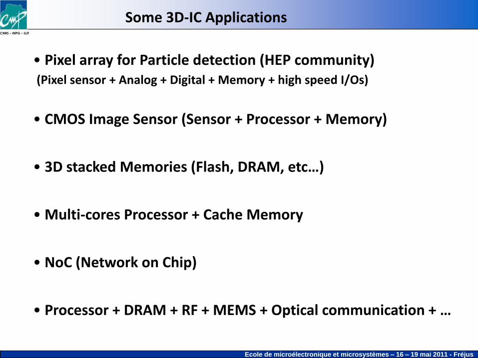
Some 3D-IC Applications
• Pixel array for Particle detection (HEP community) (Pixel sensor + Analog + Digital + Memory + high speed I/Os)
• CMOS Image Sensor (Sensor + Processor + Memory)
• 3D stacked Memories (Flash, DRAM, etc…)
• Multi-cores Processor + Cache Memory
• NoC (Network on Chip)
• Processor + DRAM + RF + MEMS + Optical communication + …

CNRS – INPG – UJF
Ecole de microélectronique et microsystèmes – 16 – 19 mai 2011 - Fréjus
The more design automation is performed on the 3rd dimension, the more is the 3D-IC Integration.
2 D
2.5 D
Memory Stack
2.1 D
2.2 D
2.3 D
2.4 D
Simple Imaging Sensor
Pixel Sensor (HEP)
Multi-Processors + Memory
NoC
3 D
2.6 D
2.7 D
2.8 D Processor + DRAM + RF + MEMS + Optical communication
2.9 D
Design Methodology
System Complexity

CNRS – INPG – UJF
Ecole de microélectronique et microsystèmes – 16 – 19 mai 2011 - Fréjus
CMC-CMP-MOSIS Collaboration

CNRS – INPG – UJF
Ecole de microélectronique et microsystèmes – 16 – 19 mai 2011 - Fréjus

CNRS – INPG – UJF
Ecole de microélectronique et microsystèmes – 16 – 19 mai 2011 - Fréjus
• Stimulate the activity by sharing the expenses for manufacturing.
• Join forces for the technical support, and dedicate the roles for each partner.
• Make easier the tech support for local users respectively by each local center.
• Because there is no standard for the 3D-IC integration, it is urgent to setup an
infrastructure making possible a broad adoption of 3D-ICs. That will have a
beneficial effect on prices, more frequent MPW runs, and more skilled engineers.
Benefits for a global Infrastructure
CMC / CMP / MOSIS partnering for 3D-IC process access

CNRS – INPG – UJF
Ecole de microélectronique et microsystèmes – 16 – 19 mai 2011 - Fréjus
CMC-CMP-MOSIS partnering on 3D-IC
CMP/CMC/MOSIS partner to introduce a 3D-IC process
Grenoble, France, 22 June 2010, CMP/CMC/MOSIS are partnering to offer a 3D-IC
MPW service based on Tezzaron’s SuperContact technology and GLOBALFOUNDRIES
130nm CMOS.
The first MPW run is scheduled to 31 May 2011:
- 2-tier face-to-face bonded wafers
- 130nm CMOS process for both tiers
- Top tier exposing TSV and backside metal pads for wire bonding.
A design-kit supporting 3D-IC design with standard-cells and IO libraries is available.
Further MPW runs will be scheduled supporting process flavors (multiple tiers beyond
2, different CMOS flavors for different tiers, ...) driven by user requirements.
Potential users are encouraged to contact CMP for details : [email protected]

CNRS – INPG – UJF
Ecole de microélectronique et microsystèmes – 16 – 19 mai 2011 - Fréjus
CMC - CMP - MOSIS Cooperation • CMC supporting Canadian Customers • CMP supporting European Customers • MOSIS supporting US Customers • Each may support other locations

CNRS – INPG – UJF
Ecole de microélectronique et microsystèmes – 16 – 19 mai 2011 - Fréjus
Tezzaron 2-Tier Process (130nm CMOS)
Process Overview

CNRS – INPG – UJF
Ecole de microélectronique et microsystèmes – 16 – 19 mai 2011 - Fréjus
Tezzaron Process Flow for TSV and DBI (using Via Middle process)
Starting wafer in 130nm (5 Cu metal layers + 6th Cu metal as DBI)
Source Tezzaron

CNRS – INPG – UJF
Ecole de microélectronique et microsystèmes – 16 – 19 mai 2011 - Fréjus
Tezzaron Process Flow for TSV and DBI (using Via Middle process)
Cu Cu Cu
Cu
Cu
Cu
Cu Cu
Cu
Cu
Cu

CNRS – INPG – UJF
Ecole de microélectronique et microsystèmes – 16 – 19 mai 2011 - Fréjus
A Closer Look at Wafer-Level Stacking
Dielectric(SiO2/SiN)
Gate Poly
STI (Shallow Trench Isolation)
Oxide
Silicon
W (Tungsten contact & via)
Cu (M1 – M5)
Cu (M6, Top Metal)
“Super-Contact”
Source Tezzaron

CNRS – INPG – UJF
Ecole de microélectronique et microsystèmes – 16 – 19 mai 2011 - Fréjus
Next, Stack a Second Wafer & Thin:
Source Tezzaron

CNRS – INPG – UJF
Ecole de microélectronique et microsystèmes – 16 – 19 mai 2011 - Fréjus
Top Tier
(10um thickness)
Bottom Tier
(Handle wafer)
Resulting 2-tier 3D-IC integration TSV and DBI (Via Middle Process)
DBIs continuing the stacking
Source Tezzaron

CNRS – INPG – UJF
Ecole de microélectronique et microsystèmes – 16 – 19 mai 2011 - Fréjus
Top Tier
(10um thickness)
Bottom Tier
(Handle wafer)
Resulting 2-tier 3D-IC integration TSV and DBI (Via Middle Process)
Bond pad for wire bonding or bump, flip-chip …
Source Tezzaron

CNRS – INPG – UJF
Ecole de microélectronique et microsystèmes – 16 – 19 mai 2011 - Fréjus
3D-IC MPW runs

CNRS – INPG – UJF
Ecole de microélectronique et microsystèmes – 16 – 19 mai 2011 - Fréjus
3D-IC Potential Users
HEP Labs
3D-IC MPW Initial Infrastructure
First MPW Run organized by FermiLab using an Industrial Process
Clustering Manufacturing

CNRS – INPG – UJF
Ecole de microélectronique et microsystèmes – 16 – 19 mai 2011 - Fréjus
Source FermiLab (3D Consortium Meeting)
MPW Full Frame
Notice Symmetry about vertical center line
Test chips: TX, TY 2.0 x 6.3 mm
Top tiers Bottom Tiers
Subreticules: A, B, C, D, E, F, G, H, I, J 5.5 x 6.3 mm
3D Consortium : 1st MPW run

CNRS – INPG – UJF
Ecole de microélectronique et microsystèmes – 16 – 19 mai 2011 - Fréjus
3D-IC Users
3D-IC MPW Infrastructure
CMC-CMP-MOSIS partnering to offer 3D-IC MPW runs
Clustering Manufacturing
Critical mass will allow frequent MPW runs and low pricing
In discussion

CNRS – INPG – UJF
Ecole de microélectronique et microsystèmes – 16 – 19 mai 2011 - Fréjus
CMP/MOSIS/CMC : 1st MPW run
MPW run deadline : May 31st, 2011

CNRS – INPG – UJF
Ecole de microélectronique et microsystèmes – 16 – 19 mai 2011 - Fréjus
3D-IC Design Platform

CNRS – INPG – UJF
Ecole de microélectronique et microsystèmes – 16 – 19 mai 2011 - Fréjus
Tezzaron / GlobalFoundries Design Platform
• The Design Platform is modular. It has all features for full-custom design or semi-custom automatic generation design.
• PDK : Original PDK from GF + (TSV / DBI) definition
• Libraries : CORE and IO standard libraries from ARM
• Memory compilers : SPRAM, DPRAM and ROM from ARM
• 3D-IC Utilities : Contributions developments embedded in the platform
• Tutorials, User’s setup.
• All the modules inside the platform refer to a unique variable, making it portable to any site. The installation procedure is straightforward.
• Support of CDB and OpenAccess databases.

CNRS – INPG – UJF
Ecole de microélectronique et microsystèmes – 16 – 19 mai 2011 - Fréjus
BacksideBondPads1_1.pdf Tezzaron Backside Bond Pad Rules (rev. 1.1 / 4 June 2009)
Bond_Interface_Rules_1_0.pdf Bond Interface Rules (rev. 1.0 / 18 July 2007)
MPW100109_Design_Guide_8.pdf MPW100109 Design Guide (rev. 8 / 11 Feb. 2010)
SuperContact_Rules_2_11.pdf SuperContact Rules (rev. 2.1 / 29 Jan 2008)
mpwMemSpec1_5.pdf MPW100109 Memory specifications (rel. 1.5 / 16 Feb. 2010)
yi_108_dr001_1t.pdf Release notes of the 130nm CMOS Design Rules Manual (version 1T)
yi_108_dr001_1t_oct2010.pdf 130nm CMOS Design Rules Manual (version 1T / Oct. 2010)
yi_108_ep004_1d.pdf Release notes of the 130nm CMOS Electrical Parameters (version 1D)
yi_108_ep004_rev_1d.pdf 130nm CMOS Electrical Parameters (version 1D / 19 March 2010)
Black : GlobalFoundries Design Documents Blue : Tezzaron Design Documents Red : Tezzarom Design guide
Tezzaron / GlobalFoundries Design Platform
Design documents included in the platform
CNRS – INPG – UJF
Ecole de microélectronique et microsystèmes – 16 – 19 mai 2011 - Fréjus
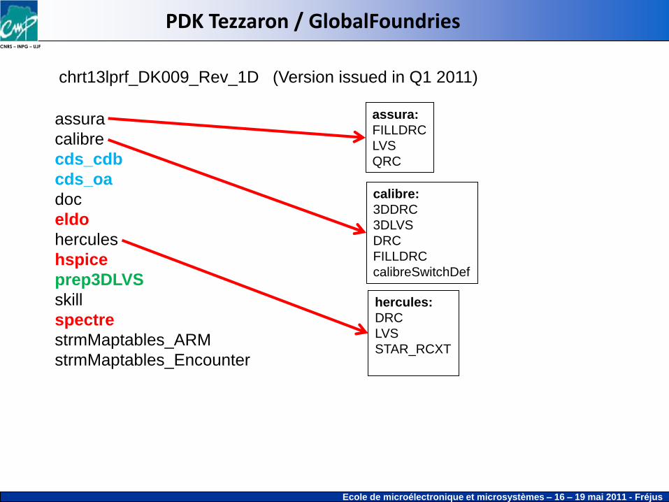
assura
calibre
cds_cdb
cds_oa
doc
eldo
hercules
hspice
prep3DLVS
skill
spectre
strmMaptables_ARM
strmMaptables_Encounter
chrt13lprf_DK009_Rev_1D (Version issued in Q1 2011)
calibre:
3DDRC
3DLVS
DRC
FILLDRC
calibreSwitchDef
assura:
FILLDRC
LVS
QRC
hercules:
DRC
LVS
STAR_RCXT
PDK Tezzaron / GlobalFoundries

CNRS – INPG – UJF
Ecole de microélectronique et microsystèmes – 16 – 19 mai 2011 - Fréjus
DBI (direct bonding interface) cells library. (FermiLab)
3D Pad template compatible with the ARM IO lib. (IPHC)
Preprocessor for 3D LVS / Calibre (NCSU)
Skill program to generate an array of labels (IPHC)
Calibre 3D DRC (Univ. of Bonn)
Dummies filling generator under Assura (CMP)
Basic logic cells and IO pads (FermiLab)
Floor-planning / automatic Place & Route using DBIs, and TSVs (CMP)
Skill program generating automatically sealrings and scribes (FermiLab)
MicroMagic PDK (Tezzaron/NCSU)
Collaborative Work to the Design Platform
HEP labs contributing with Programs, Libraries, and Utilities. All included in the Design Platform

CNRS – INPG – UJF
Ecole de microélectronique et microsystèmes – 16 – 19 mai 2011 - Fréjus
Virtuoso Layout Editor with 3D layers and verification
TSV
Back Metal
Back Pad
DBI
Assura
Calibre
Virtuoso from Cadence IC 5.1.41

CNRS – INPG – UJF
Ecole de microélectronique et microsystèmes – 16 – 19 mai 2011 - Fréjus
Virtuoso from Cadence IC 6.1.4
Customized Menu with some utilities

CNRS – INPG – UJF
Ecole de microélectronique et microsystèmes – 16 – 19 mai 2011 - Fréjus
Utility to change automatically from GF colors to new colors

CNRS – INPG – UJF
Ecole de microélectronique et microsystèmes – 16 – 19 mai 2011 - Fréjus
Libraries from Providers and Users
ARM
GF/TSC
FermiLab
IPHC
Univ. Bonn
NCSU
CNRS – INPG – UJF
Ecole de microélectronique et microsystèmes – 16 – 19 mai 2011 - Fréjus
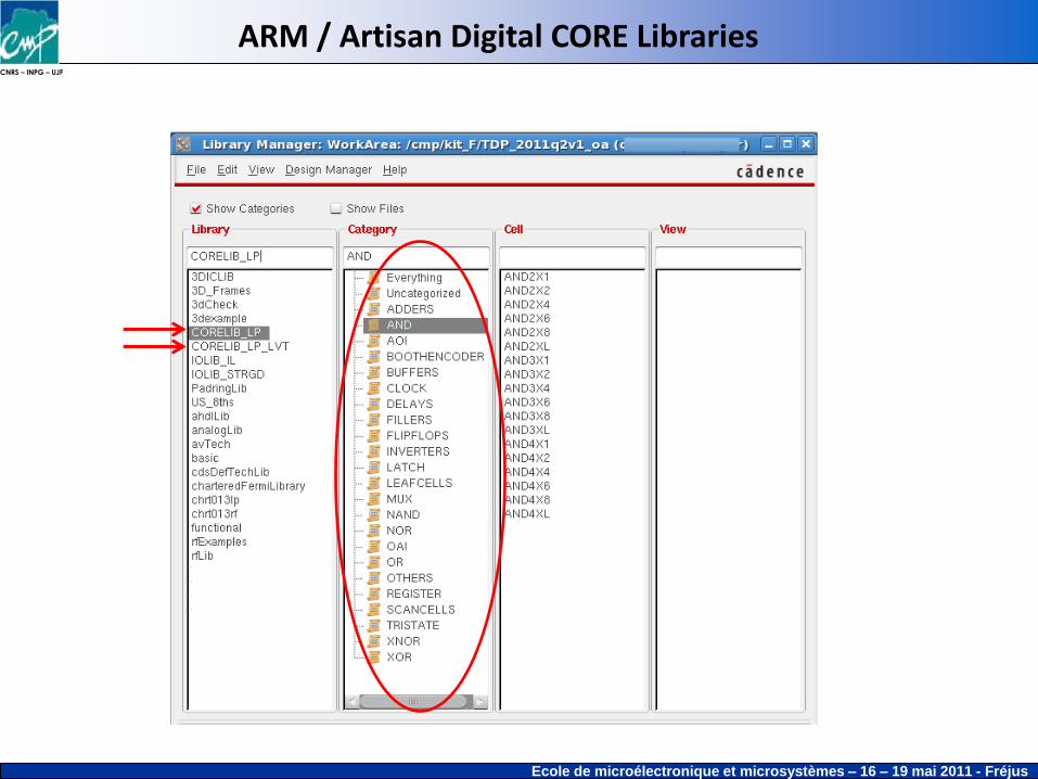
ARM / Artisan Digital CORE Libraries

CNRS – INPG – UJF
Ecole de microélectronique et microsystèmes – 16 – 19 mai 2011 - Fréjus
ARM / Artisan Digital & Analog IO Libraries
CNRS – INPG – UJF
Ecole de microélectronique et microsystèmes – 16 – 19 mai 2011 - Fréjus
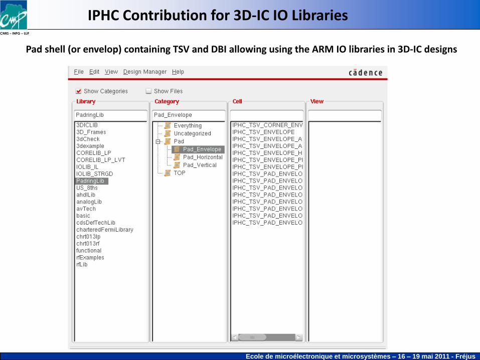
IPHC Contribution for 3D-IC IO Libraries
Pad shell (or envelop) containing TSV and DBI allowing using the ARM IO libraries in 3D-IC designs

CNRS – INPG – UJF
Ecole de microélectronique et microsystèmes – 16 – 19 mai 2011 - Fréjus
IPHC Contribution for 3D-IC IO Libraries
Pad shell (or envelop) containing TSV and DBI allowing using the ARM IO libraries in 3D-IC designs

CNRS – INPG – UJF
Ecole de microélectronique et microsystèmes – 16 – 19 mai 2011 - Fréjus
IPHC Contribution for 3D-IC IO Libraries
Pad shell (or envelop) containing DBI and TSV connecting the pad to the backside bonding pad

CNRS – INPG – UJF
Ecole de microélectronique et microsystèmes – 16 – 19 mai 2011 - Fréjus
FermiLab Digital Library
Basic custom digital cells and IO pads

CNRS – INPG – UJF
Ecole de microélectronique et microsystèmes – 16 – 19 mai 2011 - Fréjus
Virtuoso / Calibre 3D DRC Interactive Menu

CNRS – INPG – UJF
Ecole de microélectronique et microsystèmes – 16 – 19 mai 2011 - Fréjus
Virtuoso / Calibre DRC Interactive Menu
Setting switches graphically

CNRS – INPG – UJF
Ecole de microélectronique et microsystèmes – 16 – 19 mai 2011 - Fréjus
Choosing 2D or 3D LVS
Virtuoso / Calibre LVS Interactive Menu
CNRS – INPG – UJF
Ecole de microélectronique et microsystèmes – 16 – 19 mai 2011 - Fréjus
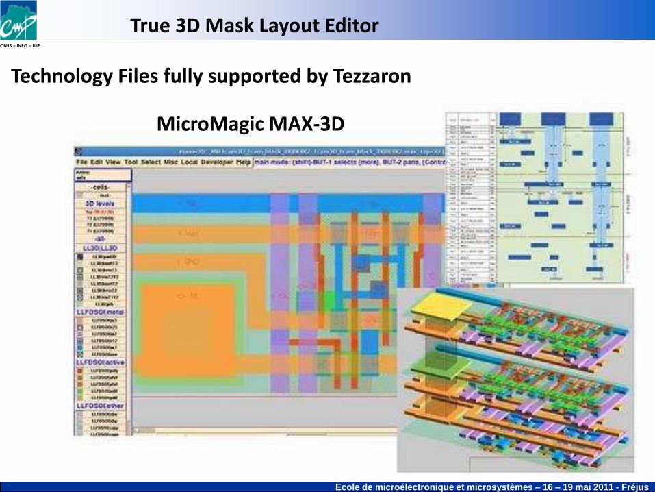
True 3D Mask Layout Editor
MicroMagic MAX-3D
Technology Files fully supported by Tezzaron
CNRS – INPG – UJF
Ecole de microélectronique et microsystèmes – 16 – 19 mai 2011 - Fréjus
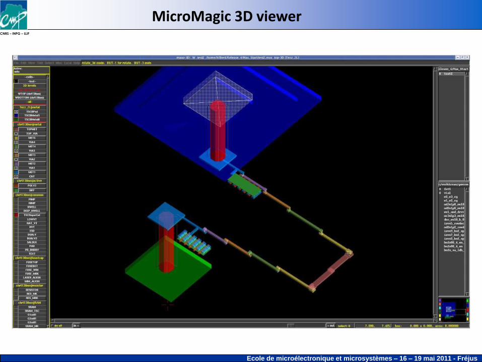
MicroMagic 3D viewer

CNRS – INPG – UJF
Ecole de microélectronique et microsystèmes – 16 – 19 mai 2011 - Fréjus
MicroMagic 3D crossection
CNRS – INPG – UJF
Ecole de microélectronique et microsystèmes – 16 – 19 mai 2011 - Fréjus
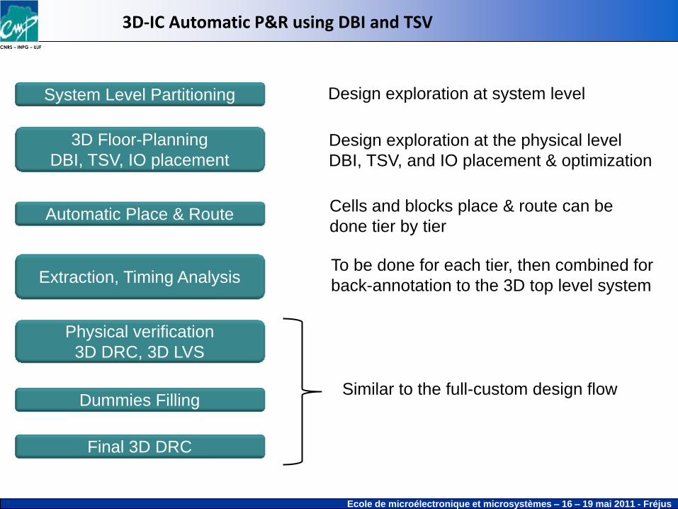
3D-IC Automatic P&R using DBI and TSV
3D Floor-Planning
DBI, TSV, IO placement
System Level Partitioning
Automatic Place & Route
Extraction, Timing Analysis
Physical verification
3D DRC, 3D LVS
Dummies Filling
Final 3D DRC
Design exploration at system level
Design exploration at the physical level
DBI, TSV, and IO placement & optimization
Cells and blocks place & route can be
done tier by tier
To be done for each tier, then combined for
back-annotation to the 3D top level system
Similar to the full-custom design flow

CNRS – INPG – UJF
Ecole de microélectronique et microsystèmes – 16 – 19 mai 2011 - Fréjus
Automatic P&R with Direct Bond Interface
DBI completely routed down to the lower metal layers
DBI array generation + P&R
- Encounter natively refuses to make the routing for pins on DBIs. - Custom scripts solved the problem. It’s a workaround. - The resulting layout is compliant to the Tezzaron DRC, LVS etc …

CNRS – INPG – UJF
Ecole de microélectronique et microsystèmes – 16 – 19 mai 2011 - Fréjus
Saving the floor plan for the bottom tier, and apply it for top tier so the automatic Place & Route run the placement and routing taking into account the DBI locations. The place & route for both tiers is optimal for timing, buffer sizing and power performance.
This should result in a “correct by construction” design.
Automatic P&R with Direct Bond Interface

CNRS – INPG – UJF
Ecole de microélectronique et microsystèmes – 16 – 19 mai 2011 - Fréjus
Cadence / Encounter v 8.1 Bump Array Generator

CNRS – INPG – UJF
Ecole de microélectronique et microsystèmes – 16 – 19 mai 2011 - Fréjus
Cadence / Encounter v 8.1 Signal Bumps Assignment

CNRS – INPG – UJF
Ecole de microélectronique et microsystèmes – 16 – 19 mai 2011 - Fréjus
Before
Before
After
After
Custom Scripts Enabling Routing on DBIs
Placing logical pins on bumps
(DBIs), and extract their location.
Generating Physical pins from these
locations.
They can now be used as terminals for
routing.

CNRS – INPG – UJF
Ecole de microélectronique et microsystèmes – 16 – 19 mai 2011 - Fréjus
- DBIs Placement
- TSVs Placement
- Obstructions on TSVs
- Std cells Placement
- Clock Tree Synthesis Filler Cells Placement
- Clock routing
- Final routing
Automatic P & R Design Flow (From Floor-Plan to Routed Design)

CNRS – INPG – UJF
Ecole de microélectronique et microsystèmes – 16 – 19 mai 2011 - Fréjus
Clock and all nets routing is enabled on M1-M5

CNRS – INPG – UJF
Ecole de microélectronique et microsystèmes – 16 – 19 mai 2011 - Fréjus
Access to the Design-Rules and the Design Platform
Customer Request
Signed NDA reception NDA
http://cmp.imag.fr
Foundry’s Agreement
Yes
Design kit &
Design Rules access
NDA Edition
Request to access from CMP Web page or by E-mail to :
[email protected] The user receive by E-mail the NDA + ARM lirary Addendum. The user sign and return by post 2 original signed copies CMP forward to Tezzaron the NDAs. When Tezzaron is OK, they counter-sign and return one copy to CMP. CMP return the copy to the user and give the access to the DRM and Design-Platform.

CNRS – INPG – UJF
Ecole de microélectronique et microsystèmes – 16 – 19 mai 2011 - Fréjus
CPPM, Marseille IPHC, Strasbourg LAL, Orsay LPNHE, Paris IRFU, CEA Saclay LAPP, Annecy-Le-Vieux * ENSTA PARISTECH, Paris * ISEA, Toulouse INFN, Roma INFN, Pavia INFN, Pisa University of Bologna * University of Perugia University of Bonn, Germany University of Barcelona, Spain IMSE-CNM-CSIC, Sevilla, Spain University of Turku, Finland Acreo AB, Norrköping, Sweden Norwegian University, Trondheim, Norway
More than 19 Users in Europe
Tezzaron Semiconductor, USA FermiLab, USA North Carolina State University, USA MOSIS, USA CMC Microsystems, Canada University of Sherbrooke, Canada + Other centers supported by MOSIS and CMC Not listed here.
Users having access to the Design Platform
Italy
France
New Users

CNRS – INPG – UJF
Ecole de microélectronique et microsystèmes – 16 – 19 mai 2011 - Fréjus
Conclusion
A very collaborative work has been achieved and still ongoing between the parties
CMC, CMP, MOSIS, FermiLab, Tezzaron, HEP Labs, NCSU.
A Design Platform resulted from the collaboration.
(Industrial CAD vendors just starting addressing the features)
First MPW run deadline : May 31st, 2011
The community is awaiting for new CAD tools dedicated to 3D-IC Integration :
+ 3D-IC Partitioning : both at the system level and the floor-planning level.
+ Sign-off tools for 3D-IC Integration : (3D-DRC, 3D-LVS, 3D-Extration)