3904 - pingjingsemi.com
TRANSCRIPT

Absolute Maximum Ratings Ratings at 25℃ ambient temperature unless otherwise specified.
Equivalent Circuit
Features For switching and amplifier applications
Marking Code
Parameter Symbol Value UnitCollector Base Voltage VCBO 60 V
Collector Emitter Voltage VCEO 40 V
Emitter Base Voltage VEBO 6 V
Collector Current IC 200 mA
Maximum Power Dissipation PD 1 W
Junction Temperature TJ 150 ℃
Storage Temperature Range TSTG -55 to +150 ℃
MMDT3904SG Double NPN Transistors
1 / 6www.pingjingsemi.com Revision:1.0 Oct-2021
1.B1
2.E2
3.B2
4.C2
5.E1
6.C1
SOT-23-6
3904
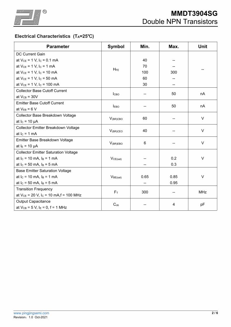
Electrical Characteristics (TA=25℃)
MMDT3904SG Double NPN Transistors
2 / 6www.pingjingsemi.com Revision:1.0 Oct-2021
Parameter Symbol Min. Max. UnitDC Current Gainat VCE = 1 V, IC = 0.1 mAat VCE = 1 V, IC = 1 mAat VCE = 1 V, IC = 10 mAat VCE = 1 V, IC = 50 mAat VCE = 1 V, IC = 100 mA
HFE
40701006030
----300----
--
Collector Base Cutoff Currentat VCB = 30V
ICBO -- 50 nA
Emitter Base Cutoff Currentat VEB = 6 V
IEBO -- 50 nA
Collector Base Breakdown Voltageat IC = 10 μA
V(BR)CBO 60 -- V
Collector Emitter Breakdown Voltageat IC = 1 mA
V(BR)CEO 40 -- V
Emitter Base Breakdown Voltageat IE = 10 μA
V(BR)EBO 6 -- V
Collector Emitter Saturation Voltageat IC = 10 mA, IB = 1 mAat IC = 50 mA, IB = 5 mA
VCE(sat) ----
0.20.3
V
Base Emitter Saturation Voltageat IC = 10 mA, IB = 1 mAat IC = 50 mA, IB = 5 mA
VBE(sat) 0.65--
0.850.95
V
Transition Frequencyat VCE = 20 V, IC = 10 mA,f = 100 MHz
FT 300 -- MHz
Output Capacitanceat VCB = 5 V, IE = 0, f = 1 MHz
Cob -- 4 pF
MMDT3904SG Double NPN Transistors
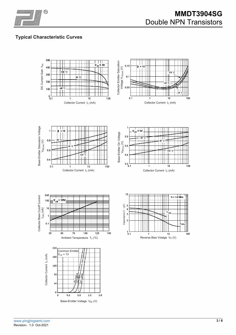
Typical Characteristic Curves
3 / 6www.pingjingsemi.com Revision:1.0 Oct-2021
Collector Current IC (mA)Collector Current IC (mA)
Collector Current IC (mA)Collector Current IC (mA)
Col
lect
or B
ase
Cut
off C
urre
nt I C
BO (n
A)C
olle
ctor
Cur
rent
IC (m
A)
Base-Emitter Voltage VBE (V)
Ambient Temperature Ta (℃) Reverse Bias Volatge VR (V)
Cap
acita
nce
C (
pF)
Base
-Em
itter
Sat
urat
ion
Volta
ge
V BE(
sat) (
V)
Base
-Em
itter
On
Volta
ge
V BE(
on) (
V)C
olle
ctor
-Em
itter
Sat
urat
ion
Volta
ge V
CE(
sat) (
V)
DC
Cur
rent
Gai
n h
FE
Common Emitter VCE = 1V

MMDT3904SG Double NPN Transistors
Ordering InformationDevice Package Shipping
MMDT3904SG SOT-23-6 3,000PCS/Reel&7inches
Package Outline
SOT-23-6 Dimensions in mm
4 / 6www.pingjingsemi.com Revision:1.0 Oct-2021
R0.15MAX
0.127
+0.05/-0.02
R0.15MAX
0.06
±0.0
512
10
0.65
±0.11.
1±0.1
10
12
2.92
2.8
±0.
1
1.6
±0.1
0.95±0.1 0.35±0.05
1.9±0.1
±0.1

Conditions of Soldering and Storage
Recommended condition of reflow soldering
Recommended peak temperature is over 245 OC. If peak temperature is below 245 OC, you may adjust the following parameters:
Time length of peak temperature (longer) Time length of soldering (longer) Thickness of solder paste (thicker)
Conditions of hand soldering
Temperature: 370 OC Time: 3s max. Times: one time
Storage conditions
Temperature5 to 40 OC
Humidity30 to 80% RH
Recommended periodOne year after manufacturing
MMDT3904SG Double NPN Transistors
5 / 6www.pingjingsemi.com Revision:1.0 Oct-2021

6 / 6www.pingjingsemi.com Revision:1.0 Oct-2021
Package Specifications The method of packaging
MMDT3904SG Double NPN Transistors
30,000 pcs per box10 reels per box
120,000 pcs per carton 4 boxes per carton
3,000 pcs per reel
Embossed tape and reel data
Symbol
B
Ø 54.5±0.2C
12.3±0.3D 9.6+2/-0.3T1 1.0±0.2T2 1.2±0.2
AValue (unit: mm)
EF
Ø 177.8±12.7±0.2
Ø 13.5±0.2
Reel (7'')
A
B
C
E
F
T1
D
T2
Cover Tape
Carrier Tape
Tape (8mm)
4.00±0.10 2.00±0.05 1.55±0.05
1.75±0.10
3.50±0.05
8±0.10
4.00±0.101.10±0.10 Pin1
SOT-23-6