384 ieee transactions on very large scale …online.sfsu.edu/mahmoodi/papers/paper_j7.pdf384 ieee...
TRANSCRIPT

384 IEEE TRANSACTIONS ON VERY LARGE SCALE INTEGRATION (VLSI) SYSTEMS, VOL. 13, NO. 3, MARCH 2005
Low-Power Scan Design UsingFirst-Level Supply Gating
Swarup Bhunia, Student Member, IEEE, Hamid Mahmoodi, Student Member, IEEE, Debjyoti Ghosh,Saibal Mukhopadhyay, Student Member, IEEE, and Kaushik Roy, Fellow, IEEE
Abstract—Reduction in test power is important to improve bat-tery lifetime in portable electronic devices employing periodic self-test, to increase reliability of testing, and to reduce test cost. Inscan-based testing, a significant fraction of total test power is dissi-pated in the combinational block. In this paper, we present a novelcircuit technique to virtually eliminate test power dissipation incombinational logic by masking signal transitions at the logic in-puts during scan shifting. We implement the masking effect by in-serting an extra supply gating transistor in the supply to groundpath for the first-level gates at the outputs of the scan flip-flops. Thesupply gating transistor is turned off in the scan-in mode, essen-tially gating the supply. Adding an extra transistor in only one logiclevel renders significant advantages with respect to area, delay, andpower overhead compared to existing methods, which use gatinglogic at the output of scan flip-flops. Moreover, the proposed gatingtechnique allows a reduction in leakage power by input vector con-trol during scan shifting. Simulation results on ISCAS89 bench-marks show an average improvement of 62% in area overhead,101% in power overhead (in normal mode), and 94% in delay over-head, compared to the lowest cost existing method.
Index Terms—Low power test, scan design, supply gating.
I. INTRODUCTION
POWER dissipation during test mode can be significantlyhigher than that during functional mode, since the input
vectors during functional mode are usually strongly correlatedcompared to statistically independent consecutive input vectorsduring testing. Zorian [1] showed that the test power could betwice as high as the power consumed during the normal mode.Test power is an important design concern to increase batterylifetime in hand-held electronic devices that incorporate built-inself test (BIST) circuitry for periodic self-test. It is also impor-tant to improve test cost, since reduced test power of a moduleallows parallel testing of multiple embedded cores in an IC [7].Increased peak power is likely to create noise problems in a chipby causing a drop in the supply voltage [9]. Peak and averagepower reduction during test contributes to enhanced reliabilityof the test and improvement of yield [11]. It is, therefore, im-portant to ensure reduction in power dissipation during the testmode.
Scan architectures represent the prevalent Design for Testa-bility (DFT) approach to test digital circuits [9]. During test ap-
Manuscript received July 28, 2004; revised November 13, 2004. This researchwas supported in part by the GSRC Marco Center.
S. Bhunia, H. Mahmoodi, S. Mukhopadhyay, and K. Roy are with the Schoolof Electrical and Computer Engineering, Purdue University, West Lafayette, IN47907-1285 USA (e-mail: [email protected]).
D. Ghosh is with Analog Devices, Norwood, MA 02060 USA.Digital Object Identifier 10.1109/TVLSI.2004.842885
plication in a scan-based circuit, power is dissipated in boththe sequential scan elements and in the combinational logic.While scan values are loaded into a scan chain, the effect ofscan-ripple propagates to the combinational block and redun-dant switching occurs in the combinational gates during the en-tire scan-in/out period. It is observed that about 78% of totaltest energy is dissipated in the combinational block alone [10].Hence, a low-power scan design should address techniques toreduce power dissipation in the combinational block.
There has been multitude of research exploring efficienttechniques to reduce test power in scan-based circuits. Wanget al. proposed automatic test pattern generation technique toredesign test vectors for reducing power dissipation during scantesting [4]. With their automatic test pattern generation (ATPG),redundant transitions in combinational logic can be reducedbut not completely eliminated. Moreover, test application timemay increase to trade off power. Scan-latch reordering [5] orinput vector reordering [6] techniques have been proposedfor reduction in test power. However, these techniques targetreduction of transitions at the output of scan flip-flops andcannot eliminate redundant switching in combinational block.In [7], Whetsel provided a solution for reduction in averageand peak power dissipation by transforming conventional scanarchitecture into desired number of selectable, separate scanpaths. Each scan path is in turn filled with stimulus and emptiedof response. Sankaralingam et al. [8] proposed a solution tothe peak power problem during external testing by selectivelydisabling the scan chain. In this scheme, the test-set is gen-erated and ordered in such a way that only changing portionsof consecutive tests are shifted into the scan chains. In [11]and [12], the authors provide a solution to prevent peak powerviolation during both shift and capture cycle using scan chainpartitioning. However, the modification of the scan flip-flop in[12] results in a substantial increase in area and degradation inperformance. Redundant power loss in combinational logic isnot completely prevented in the above cases, since part of thescan chain is always active during shifting.
Inserting blocking logic into the stimulus path of the scanflip-flops [as shown in Fig. 1(a)] to prevent propagation of scan-ripple effect to logic gates offers a simple and effective solutionto significantly reduce test power, independent of test set. Wers-tendorfer et al. have proposed NOR or NAND gate-based blockingmethod in [10]. Blocking gates (of type NOR or NAND) are con-trolled by the test enable signal [as in Fig. 1(b)], and the stim-ulus paths remain fixed at either logic “0” or logic “1” duringthe entire scan shift operation. Zhang et al. [14] have used mul-tiplexers at the output of the scan cells [Fig. 1(b)], which hold
1063-8210/$20.00 © 2005 IEEE
Authorized licensed use limited to: San Francisco State Univ. Downloaded on December 10, 2008 at 17:49 from IEEE Xplore. Restrictions apply.

BHUNIA et al.: LOW-POWER SCAN DESIGN USING FIRST-LEVEL SUPPLY GATING 385
Fig. 1. (a) Scan architecture with existing blocking circuitry to reduce power during scan operation. (b) Blocking logic.
the previous states of the scan register during shifting and, thus,prevent activity in combinational logic. Another method for re-duction in combinational power using blocking is to use a scan-hold circuit as a sequential element. This technique is called en-hanced scan [9], which also helps in delay fault testing by al-lowing application of arbitrary two-pattern test. In a scan-holddesign, each sequential element contains an additional storagecell called the hold latch, and the stimulus path for the combina-tional part is connected to the output of the hold latch, which isnot used in scan shifting. Therefore, it also prevents redundantswitching in combinational logic.
The problem with the blocking logic is that it adds signifi-cant delay in the signal propagation path from the scan flip-flopto logic [10]. Moreover, they have large overhead in terms ofarea and switching power in normal operation of the circuit.In this paper, we present an elegant signal blocking technique,which is referred as First-Level Supply (FLS) gating, to re-duce power dissipation in the combinational logic during scanshifting. This is achieved by inserting a supply gating transistorin the first level of logic connected to the scan cell outputs,which essentially “gates” the VDD or GND line. The proposedmethod is as effective as the other blocking methods in terms ofreducing peak power and total energy dissipation during scantesting. However, since we introduce just one transistor in thecharge/discharge path of the first level logic, the delay penaltyis significantly reduced compared to other blocking methods,which insert additional level of logic into signal propagation
path. The overhead incurred in die-area and switching powerin normal mode due to extra discrete Fourier transform (DFT)logic is also significantly lower than the existing methods usingNOR [10], MUX [14], and Hold-latch [9]. The area overhead forFLS, however, depends on number of unique first-level fanoutgates. We have also presented a low-complexity algorithm to re-duce fanouts of the scan flip-flops under delay constraint, whichhelps to further reduce the area overhead in FLS.
Besides saving dynamic power in the combinational logicduring test application, FLS can also be used to reduce leakagepower by input vector control (IVC) mechanism [16]. With tech-nology scaling, leakage power is becoming a notable sourceof power dissipation. We have demonstrated that FLS can beeasily adapted to reduce leakage power in the combinational partduring scan testing without any extra hardware or control signal.Based on the advantage of leakage reduction, we have shownthat FLS even achieves improvement in total test power com-pared to other blocking methods. Since leakage increases ex-ponentially with technology scaling, we can obtain about 25%improvement in total test power in a 45-nm technology nodecompared to a NOR-based blocking scheme.
The rest of the paper is organized as follows: Section II il-lustrates the proposed gating technique for saving energy in thecombinational block during scan shifting. Section III presentsexperimental results in terms of area, delay, and power for a setof ISCAS89 benchmark circuits. Section IV explains power dis-sipation in test mode and presents a technique to reduce leakage
Authorized licensed use limited to: San Francisco State Univ. Downloaded on December 10, 2008 at 17:49 from IEEE Xplore. Restrictions apply.

386 IEEE TRANSACTIONS ON VERY LARGE SCALE INTEGRATION (VLSI) SYSTEMS, VOL. 13, NO. 3, MARCH 2005
Fig. 2. (a) Use of FLS gating transistor in combinational part. (b) Transient response in 70 nm.
power using FLS. Section V discusses further scope for opti-mizing DFT overhead and test power, and Section VI discussesimportant test issues associated with the proposed technique.Section VII concludes the paper.
II. FLS GATING FOR POWER REDUCTION IN SCAN MODE
The dynamic power dissipation in the combinational circuitcan be reduced by lowering the activity of the circuit. Previousworks on low power scan design target reducing the activity ofthe circuit by gating the inputs of the combinational block withthe use of extra logic gates (latch [9], multiplexer [14], NOR
[10], etc.). However, these techniques have a negative impacton circuit performance and considerably add to the total area.Moreover, they impose significant power overhead during thenormal mode of operation of the circuit. In this section, we havedescribed a novel methodology based on supply gating to reducepower dissipation in the combinational circuit during the scanshift cycles.
A. Supply Gating Transistor for Reducing Active Power inScan Mode
Although global supply gating transistor prevents propaga-tion of switching activity in the combinational block, it resultsin considerable area and delay overhead. To overcome theoverhead associated with the global supply gating transistor,we have proposed a novel FLS gating technique, where onlythe first-level logic gates connected to the scan flip-flops aregated using supply gating transistors [Fig. 2(a)]. Insertion of thesupply gating transistor in the first level logic will screen therest of the combinational logic from the state-input (scan-input)transitions (except only one transition—a “1” to “0” if NMOSsupply gating and “0” to “1” in PMOS supply gating). This canbe observed in Fig. 2(b) from which it can be understood thatthe first transition at the input IN from “1” to “0” will chargethe OUT1 to VDD. This transition will propagate throughout
the inverter chain. However, any further transition in the input(i.e., from “0” to “1”) will not propagate, as the OUT1 cannot bedischarged [Fig. 2(b)]. This significantly reduces the redundantactivity of the circuit during the scan-shift operation.
The principal issue associated with FLS scheme shown inFig. 2 is that the outputs of the first level gates are floating if theyare at logic “0” (connected to the virtual ground). The voltage ofa floated output is determined by the leakage balance betweenthe pull-up PMOS and pull-down NMOS network of the gate.Moreover, crosstalk noise or transient effect due to soft error caneasily change the voltage of a floated output. If the voltage of theoutput of a first-level gate is not exactly at VDD or GND, thiscould cause static short circuit current on the following logicgates being driven by the first level gate. This particularly be-comes more of an issue in deep submicron technologies due toincreased leakage and noise.
In order to avoid such an issue, the outputs of the first-levelgates need to be forced at VDD or zero in the supply gatingmode. If the GND is gated as in Fig. 2, then the outputs of thefirst-level gates can be forced to VDD by a pull-up PMOS drivenby the Gating Control (GC) signal. If the VDD is gated, thenthe outputs of the first level gates can be forced to ground usingNMOS pull-down transistors driven by the GC signal. The gen-eral schemes of the proposed supply gating are shown in Fig. 3.In order to evaluate and compare these two schemes [Fig. 3(a)and (b)], they are applied to NAND and NOR gates. The pull-up(pull-down) transistor is kept at minimum size to optimize itsimpact on circuit delay and power during normal mode of op-eration. Fig. 4 shows the delay comparisons of the gated-VDDand gated-GND circuits. As expected, for the same size of thesupply gating transistor, the gated-GND circuit is faster than thegated-VDD circuit for both NOR and NAND gates. This is becauseNMOS transistors are faster than PMOS transistors of the samesize. It is also observed that as the size of the supply gating tran-sistor is increased, the delay of the circuit is reduced and getscloser to the delay of the circuit without any gating. However,
Authorized licensed use limited to: San Francisco State Univ. Downloaded on December 10, 2008 at 17:49 from IEEE Xplore. Restrictions apply.

BHUNIA et al.: LOW-POWER SCAN DESIGN USING FIRST-LEVEL SUPPLY GATING 387
Fig. 3. Proposed supply gating schemes. (a) GND-gating. (b) VDD-gating.
Fig. 4. Delay comparison of gated-VDD and gated-GND for (a) NOR gate and (b) NAND gate.
Fig. 5. Power comparison of gated-VDD and gated-GND for (a) NOR gate and (b) NAND gate.
increasing the transistor width for the supply gating transistordoes not help much for delay improvement beyond some point.As observed from the plots in Fig. 4, for 2-input NAND and NOR
gates, a supply gating transistor of six times the minimum sizeis a reasonable choice for minimal delay impact and small areaoverhead. Another point observed from Fig. 4 is that the impactof pull-up (pull-down) transistor on delay is negligible. Fig. 5shows the power comparisons in the active mode for both theNAND and NOR gates. For the NAND gate, there is not much dif-ference in the power of the gated-VDD and gated-GND cases.
However, for the NOR gate, the gated-GND circuit shows lesspower consumption due to fewer transistors in the stack, ‘and,therefore, fewer intermediate node capacitances. From these re-sults, it can be inferred that the gated-GND is more suitable forgating due to smaller area overhead and less delay and powerpenalties. Table I compares the area, delay, and power overheadamong several gating techniques, including FLS. We can ob-serve from Table I that compared to latch and MUX-based gating,FLS is superior with respect to all three design parameters (area,delay, and power).
Authorized licensed use limited to: San Francisco State Univ. Downloaded on December 10, 2008 at 17:49 from IEEE Xplore. Restrictions apply.

388 IEEE TRANSACTIONS ON VERY LARGE SCALE INTEGRATION (VLSI) SYSTEMS, VOL. 13, NO. 3, MARCH 2005
TABLE ICOMPARISON OF AREA, DELAY, AND POWER AMONG ALTERNATIVE GATING
TECHNIQUES APPLIED TO A SINGLE INVERTER
B. Scan Design Using FLS
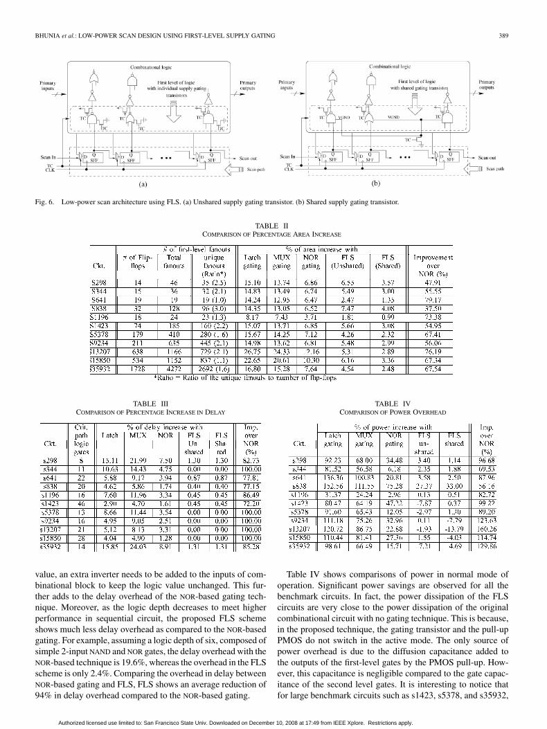
Fig. 6 shows the proposed FLS gating techniques applied toa general circuit. This scheme completely eliminates switchingactivity in the combinational circuit during scan shifting. To im-plement the proposed supply gating scheme in a scan architec-ture, two approaches can be taken: In one case, the first-levelgates have separate supply gating transistors [Unshared FLS;see Fig. 6(a)], and in the other case, all the first-level gates sharea single supply gating transistor [Shared FLS; see Fig. 6(b)]. Thearea overhead is mostly due to the active area taken by supplygating transistors. By sharing the supply gating transistors, areaoverhead can be reduced because a shared supply gating tran-sistor can have less size than the sum of the sizes of all supplygating transistors in the unshared case. In the Unshared FLS,the size of the supply gating transistor is chosen to be ten timesthe minimum transistor size, regardless of the type of the gate( ). Statistically speaking, for randominput data patterns, we can assume that approximately half of thefirst-level gates are switching at a time, while the rest do not ex-perience any switching. Therefore, the supply gating transistorsof the idle gates are not actually used, and the size of the supplygating transistor in case of Shared FLS can be half the sum ofthe sizes of all supply gating transistors in the Unshared FLS.Based on this argument, the size of the supply gating transistorin the Shared FLS case is given by
(1)
where is the number of first-level gates in the combinationalcircuit. Therefore, by sharing the supply gating transistor, thearea overhead due to supply gating transistor is reduced by half.
III. EXPERIMENTAL RESULTS AND COMPARISONS
To estimate the effectiveness of the FLS scheme, we simu-lated a set of ISCAS89 benchmark circuits and obtained powerand performance in normal mode of operations and area over-head due to additional DFT logic in case of FLS, NOR-based,MUX-based, and latch-based gating. The simulation was per-formed in the 70-nm Berkeley Predictive Technology Model(BPTM) [15] to observe the effect of gating in a sub-100-nmscaled technology. The gate-level netlists were first technology-mapped to a LEDA 0.25- standard cell library [21] using a Syn-opsys design compiler with the mapping effort at medium [19].The library contains complex gate types, e.g., “aoi” (and-or-in-vert) and “mux.” and hence, the total number of logic gates isreduced from that in the original benchmark. The benchmarkcircuits are then translated to Hspice and scaled to 70 nm. Poweris measured in NanoSim [20] by applying 100 random vectorsto the inputs, and delay is measured by Hspice simulation ofthe critical paths of a circuit. Tables II–IV show comparisons of
the proposed gating techniques with the existing techniques. Inthese tables, the advantage of our technique is shown in termsof percentages of improvement over the NOR-based gating. Thepercentage of improvement is calculated as the percentage ofreduction in overhead from the NOR-based technique ( )to our technique ( ) [see (2)].
percent improvement (2)
Table II shows comparisons of these techniques in terms ofarea overhead. Since the layout rules for the 70-nm node are notavailable, the measure used for area is the total transistor activearea ( for a transistor). As explained earlier, by sharingthe gating transistors in the Shared FLS case, the area over-head can be reduced by nearly half compared to the UnsharedFLS, since pull-up PMOS transistors are minimum sized. Thelatch is the largest gating circuit, and therefore, the latch-basedgating circuit has the largest area overhead followed by the MUX-based gating technique. The NOR-based gating has the least areapenalty among the existing gating techniques. The proposedShared FLS gating technique exhibits the smallest area overheadfor all benchmark circuits (2.7% on an average). It shows 48%to 80% reduction in area overhead (with an average of 62%)as compared to the existing NOR-based gating technique, whichhas the least area penalty among the alternative techniques. Itcan be noted that for the NOR, MUX, or Latch-based method,area overhead is proportional to the number of scan flip-flops,since blocking logic is introduced at the output of each scanflip-flop [Fig. 1(a)]. However, in FLS, gating logic is insertedin all first-level gates [Fig. 6(a)], the number of which dependson the number of unique fanout gates of the scan flip-flops.Therefore, for a circuit with large number of fanouts for thescan flip-flops, such as s838, improvement in area overhead maynot be significant (Table II). However, the number of fanouts ofa scan flip-flop is usually not high (2.3 on average as can beobtained from column 2 and 3) to satisfy delay constraint of acircuit (since higher fanout means higher load at the output ofa gate and, hence, higher delay). Due to overlapping of fanoutcones, the number of unique fanouts of the scan flip-flops, i.e.,the number of first-level gates (as shown in column 4), is furtherless (1.8 on average per scan flip-flop compared to 2.3 of totalfan-out).
Table III shows comparative impact of the existing and pro-posed gating techniques on circuit delay for different bench-mark circuits. As observed from Table III, the proposed tech-nique has the least impact (minimal increase) on circuit delay.The MUX-based gating has the largest increase in delay. Thelatch-based gating shows the second largest increase in delay,and the NOR-based gating has the least delay penalty amongexisting techniques. Compared to the NOR-based gating, whichhas the least delay penalty among existing techniques, FLS ex-hibits circuit delay reduction of up to 8%. In fact, as observedfrom Table III, the delay overhead of the FLS technique is lessthan 1.3% for all the benchmark circuits. Another point to no-tice is that the delay of the NOR-based gating would be more ifthe logic polarity at the input of combinational block needs tobe preserved. Since introduction of a NOR gate inverts the logic
Authorized licensed use limited to: San Francisco State Univ. Downloaded on December 10, 2008 at 17:49 from IEEE Xplore. Restrictions apply.
BHUNIA et al.: LOW-POWER SCAN DESIGN USING FIRST-LEVEL SUPPLY GATING 389
Fig. 6. Low-power scan architecture using FLS. (a) Unshared supply gating transistor. (b) Shared supply gating transistor.
TABLE IICOMPARISON OF PERCENTAGE AREA INCREASE
TABLE IIICOMPARISON OF PERCENTAGE INCREASE IN DELAY
value, an extra inverter needs to be added to the inputs of com-binational block to keep the logic value unchanged. This fur-ther adds to the delay overhead of the NOR-based gating tech-nique. Moreover, as the logic depth decreases to meet higherperformance in sequential circuit, the proposed FLS schemeshows much less delay overhead as compared to the NOR-basedgating. For example, assuming a logic depth of six, composed ofsimple 2-input NAND and NOR gates, the delay overhead with theNOR-based technique is 19.6%, whereas the overhead in the FLSscheme is only 2.4%. Comparing the overhead in delay betweenNOR-based gating and FLS, FLS shows an average reduction of94% in delay overhead compared to the NOR-based gating.
TABLE IVCOMPARISON OF POWER OVERHEAD
Table IV shows comparisons of power in normal mode ofoperation. Significant power savings are observed for all thebenchmark circuits. In fact, the power dissipation of the FLScircuits are very close to the power dissipation of the originalcombinational circuit with no gating technique. This is because,in the proposed technique, the gating transistor and the pull-upPMOS do not switch in the active mode. The only source ofpower overhead is due to the diffusion capacitance added tothe outputs of the first-level gates by the PMOS pull-up. How-ever, this capacitance is negligible compared to the gate capac-itance of the second level gates. It is interesting to notice thatfor large benchmark circuits such as s1423, s5378, and s35932,
Authorized licensed use limited to: San Francisco State Univ. Downloaded on December 10, 2008 at 17:49 from IEEE Xplore. Restrictions apply.
390 IEEE TRANSACTIONS ON VERY LARGE SCALE INTEGRATION (VLSI) SYSTEMS, VOL. 13, NO. 3, MARCH 2005
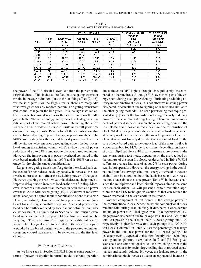
TABLE VCOMPARISON OF POWER CONSUMPTION DURING TEST MODE
the power of the FLS circuit is even less than the power of theoriginal circuit. This is due to the fact that the gating transistorresults in leakage reduction (due to the stacking effect [2], [3])for the idle gates. For the large circuits, there are many idlefirst-level gates for any random pattern. The gating transistorsreduce the leakage on the idle gates. This leakage is called ac-tive leakage because it occurs in the active mode on the idlegates. In the 70-nm technology node, the active leakage is a sig-nificant part of the overall active power. Reducing the activeleakage on the first-level gates can result in overall power re-duction for large circuits. Results for all the circuits show thatthe latch-based gating imposes the largest power overhead. TheMUX-based gating has the second largest power overhead forall the circuits, whereas NOR-based gating shows the least over-head among the existing techniques. FLS shows overall powerreduction of up to 33% compared to the NOR-based technique.However, the improvement in power overhead compared to theNOR-based method is as high as 160% and is 101% on an av-erage for the circuits under consideration.
Larger sized gating transistors for gates in the critical path canbe used to further reduce the delay penalty. It increases the areaoverhead but does not affect the switching power of the gates.However, upsizing the NOR, MUX, or latch does not help much toimprove delay since it increases load on the scan flip-flop. More-over, it comes at the cost of an increase in both area and poweroverhead. As in NOR-based gating [10], FLS allows at most twosignal changes at a gated input for application of one test vector.Hence, we virtually eliminate switching power in the combina-tional logic during scan-shift operation. Area and power over-head can be further reduced by local fanout optimization underdelay constraint, as discussed in Section V. The routing over-head associated with the proposed FLS technique should not bevery high. This is because FLS requires no additional controlsignal. The TC signal needs to be routed to the scan flip-flops ina standard scan-based design, while in the proposed technique,the gating control signal needs to be routed only to the first levelof logic.
IV. POWER IN TEST MODE
As we have seen in Section III, FLS induces some penalty interms of power dissipation in normal mode of circuit operation
due to the extra DFT logic, although it is significantly less com-pared to other methods. Although FLS saves most part of the en-ergy spent during test application by eliminating switching ac-tivity in combinational block, it is not effective in saving powerdissipated in scan chain due to rippling of scan values similar tothe other gating methods. The scan partitioning technique pre-sented in [7] is an effective solution for significantly reducingpower in the scan chain during testing. There are two compo-nents of power dissipated in scan chain: switching power in thescan element and power in the clock line due to transition ofclock. While clock power is independent of the load capacitanceat the output of the scan element, the switching power of the scanelement is almost linearly dependent on the output load. In thecase of NOR-based gating, the output load of the scan flip-flop isa NOR gate, but, for FLS, the load varies, depending on fanoutof a scan flip-flop. Hence, FLS can consume more power in thescan chain during test mode, depending on the average load onthe outputs of the scan flip-flops. As described in Table V, FLSsuffers an average increase of about 2% in scan power duringscan in/out operation. However, the energy savings in the combi-national part far outweighs the small energy overhead in the scanchain. It can be noted that both the latch-based and MUX-basedmethods have about the same power (Table V) in the scan chainsince the multiplexer and latch circuit imposes almost the sameload on their driver. We will present a fanout reduction algo-rithm for the FLS technique in Section V that can reduce thepower overhead in the scan chain in test mode.
Another component of test power is the leakage power inthe combinational block. Since the whole combinational blockremains idle during scan shifting, it dissipates a considerableamount of power due to leakage current. In our experiment, av-erage power dissipation due to leakage was 20% and 17% of thetotal test power in the case of the NOR-based gating and FLS,respectively (higher for MUX and latch gating) at a 100-MHztest clock. Column 7 in Table V lists the percentage of leakagepower in the total test power for the NOR-based gating. Theleakage power is expected to rise significantly with technologyscaling and temperature, as explained in [2] and [3]. For a givenscan chain and combinational block, the switching power in thescan chain reduces by technology scaling due to reduced capac-itances and supply voltage. However, the leakage power in thecombinational block increases due to an exponential increase in
Authorized licensed use limited to: San Francisco State Univ. Downloaded on December 10, 2008 at 17:49 from IEEE Xplore. Restrictions apply.

BHUNIA et al.: LOW-POWER SCAN DESIGN USING FIRST-LEVEL SUPPLY GATING 391
the subthreshold leakage and new mechanisms of leakage suchas gate leakage and band-to-band-tunneling junction leakage[2]. Therefore, the leakage power becomes a larger fraction ofthe total test power during scan shifting. In terms of supplynoise, leakage power on the combinational block adds as a con-stant dc component to the supply current during scan shifting.Such a dc component in the supply current results in IR-dropnoise. This noise added to the switching noise due to switchingof flip-flops can affect the reliability of the scan test. The FLStechnique holds an important advantage over the alternative im-plementations in terms of reduction in leakage power, as de-scribed in Section IV-A. We will describe how the FLS schemecan be easily adapted to save leakage during scan shifting. It isinteresting to observe that although the power in the scan chainis about 2% higher in FLS compared to the NOR-based method,significant reduction in leakage results in about a 5.3% averageimprovement in overall test power (see column 8 of Table V).
A. Leakage Reduction in Test Mode by Input Vector Control
Test vector bits are often scanned in using a slow clock to re-duce switching power consumption and the chance of errors oc-curring due to scan chain delays. This increases the scan shiftingtime and, therefore, the leakage component of energy dissipa-tion during testing. Therefore, it is important to address theleakage power issue even in the test mode.
Leakage of a combinational circuit is a strong function ofthe state of its inputs [16], [17]. Therefore, by selecting thebest input vector for a combinational circuit during the standbymode, its leakage power dissipation can be minimized. Thereare algorithms proposed in the literature for finding the bestinput vector [16], [17]. The existing gating techniques fix thestate of the inputs during shift operation. However, this inputstate may not correspond to the best input vector that mini-mizes overall leakage power on the combinational block. In thelatch and MUX-based gating techniques, the states of inputs arefixed at the state of scan flip-flops before scan shifting starts.Therefore, the state of the inputs cannot be set to the best vectorin the MUX and latch-based gating techniques. In the NOR andNAND-based gating techniques, the state of all inputs are forcedto logical “0” and “1,” respectively. However, state of all “0”or all “1” may not correspond to the best input vector. Inter-estingly, we have observed that the NAND and NOR gating canbe used together to provide best input vector for the combina-tional block during scan shifting. In this case, the NOR maskingis used at the inputs that are to be at the logic state of “0,” andNAND masking is used at the inputs that are to be at the logicstate of “1” to generate the best input vector. It can be noted thatinverted masking signals are required to gate the NOR and NAND
gates. Although this mixed use of NOR and NAND gating can in-duce the minimum leakage state in the combinational block, theblocking gates (NAND and NOR) themselves consume leakagepower. The application of the best vector by the FLS can resultin more leakage savings, because FLS does not introduce extragates to mask the input switching.
In the proposed FLS scheme of Fig. 3(a) or (b), the out-puts of the all first-level gates are forced to logic level “1” or“0,” respectively. However, this state of inputs may not corre-spond to the best input vector for minimum leakage. By se-lective use of gated-GND [Fig. 3(a)] or gated-VDD [Fig. 3(b)]
Fig. 7. Leakage reduction with supply gating and input vector control. Gatingtransistors are shared among gating of the same type (i.e., with gated-VDD orgated-GND).
for individual inputs, the state of the circuit can be assigned tothe best input vector during the scan test in order to minimizeleakage power dissipation on the combinational circuit. Fig. 7shows the scan architecture with input vector control using FLS.It is worth noting that sharing of the gating transistors is stillpossible. However, to avoid a possible short-circuit condition,sharing has to be limited between logic gates with similar gating,i.e., all the NMOS GND-gating transistors can be shared amongthe GND-gated first-level gates, and all the PMOS VDD-gatingtransistors can be shared among the VDD-gated first-level gates(see Fig. 7). In this case, an inverted gating control signal is re-quired to control the PMOS VDD-gating transistors.
The results of leakage savings by input vector control usingmixed NOR/NAND and mixed gated GND/VDD FLS for differentbenchmark circuits are shown in Table VI. The best input vec-tors are found using the algorithms described in [16]. As ob-served, depending on the benchmark, significant savings can beachieved by applying the best input vector using selective use ofgated-GND or gated-VDD FLS schemes for individual inputs.The mixed FLS gating techniques show improvements of 37%,36%, and 29% in leakage power on an average compared to theNOR, NAND, and mixed NOR/NAND masking techniques. Theseimprovements are attributed to two facts: a) FLS eliminates theextra gating logic circuits (NOR/NAND), which are also leaking,and b) FLS reduces the leakage of first-level gates due to thestacking effect. Since the leakage for a multiplexer and latch aremore than 10 higher than the NOR gate, we get more improve-ment in leakage with FLS compared to the MUX or latch-basedmethods. The leakage reduction is an additional advantage ofthe mixed FLS techniques on top of the benefits in terms of area,delay, and power in the normal mode.
Due to the exponential increase of leakage with technologyscaling and temperature increase, the leakage reduction of themixed FLS becomes more effective as the technology scales orthe temperature increases. Table VII shows the improvement inthe effectiveness of this technique in the reduction of the overalltest power with technology scaling. As the technology scalesto smaller feature sizes, the leakage power on the combinationblock becomes a larger fraction of the total test power. There-fore, leakage reduction by mixed FLS gating can result in amore dramatic saving in the total test power. As observed fromTable VII, compared to the NOR-based gating, the mixed FLSgating results in an average reduction of 5.3% in the overall
Authorized licensed use limited to: San Francisco State Univ. Downloaded on December 10, 2008 at 17:49 from IEEE Xplore. Restrictions apply.

392 IEEE TRANSACTIONS ON VERY LARGE SCALE INTEGRATION (VLSI) SYSTEMS, VOL. 13, NO. 3, MARCH 2005
TABLE VILEAKAGE POWER (�W) OF COMBINATIONAL BLOCK IN THE TEST MODE FOR DIFFERENT GATING TECHNIQUES (70-nm CMOS, Supply = 1 V, T = 25 C)
TABLE VIILEAKAGE REDUCTION BY MIXED FLS GATING IN SCALED TECHNOLOGIES
test power in the 70-nm technology. This reduction, however,improves to 25% in a more scaled technology of 45 nm. Hence,FLS outperforms alternative gating techniques in terms oftotal test power as well. Moreover, these results manifest thescalability of the proposed gating techniques across technologygenerations.
The input vector control using the FLS scheme can also bedynamically employed during the normal mode of operationswhen the combinational block is idle. In this way, the activeleakage component of power dissipation can be reduced. In thiscase, an extra control signal needs to be generated to dynami-cally gate the first-level gates during normal mode of operation.
V. FURTHER REDUCTION OF AREA/POWER OVERHEAD
In FLS, the overhead in terms of die-area and power duringnormal operation is less than in earlier methods. Transistordownsizing can be applied in all the methods, including FLS,to reduce the area and power overhead, but narrowing transistorwidth usually trades off circuit performance by affecting criticalpath delay. FLS, however, has the potential to reduce the areapenalty further without compromising delay.
Since the overhead in area and power in FLS is proportionalto the number of unique fanout cells, we can reduce the over-head by optimizing the number of direct fanouts of the scanflip-flops. The number of fanout cells in a circuit is not generallyallowed to be large, since it affects capacitive load at the outputof a cell and, hence, increases propagation delay. It can be noted
that when a netlist is mapped to a standard cell library, fanoutsof the cells may change, depending on the gate types availablein the library. Existence of complex gate types like “aoi” or“mux” tends to reduce number of fanouts. As an example, forthe benchmark s838, the number of unique fanouts is 118 fora cell library containing only inverter and 2-input NOR/NANDs,whereas this number reduces to 96 (19% improvement) whenthe netlist is technology-mapped to the complete the LEDA li-brary consisting of multi-input complex gates.
We designed a low-complexity local fanout reduction algo-rithm which targets minimization of first-level gates under con-straint on critical path delay. The algorithm is based on finding aminimal vertex cover [18] of a bi-partitite graph and then addingtwo inverters in series at the output of selected scan flip-flops.First, we create a undirected bi-partite graphwith the scan flip-flop outputs (SO) and the first-level gates(FL) as vertices. Edges in correspond to logic path from scanflip-flops to first-level gates in the netlist. Critical path edgesare marked . Then, we determine an approximate solution ofthe vertex cover problem ( ) for thegraph using a greedy heuristic-based solution of linear com-plexity. Note that the vertex cover problem, i.e., finding an op-timal vertex set that covers all the edges in a graph is NP-Hard[18]. We, however, use an approximate solution for the vertexcover problem using heuristics. First, we identify the SO ver-tices that have a single fanout and select the incident FL vertexfor them. We choose these FL vertices into VC one at a time indecreasing order of degree of the vertices and remove all theirincident edges from . Next, we choose those FL nodes withhigh degree (i.e., large number of incident edges, say three ormore) and the ones corresponding to critical path edges. As be-fore, the incident edges of all FL nodes selected in VC are re-moved from . Finally, the SO vertices with remaining degreegreater than 0 are selected into VC.
Two inverters (INV1, INV2) of appropriate sizes are addedto all the s in VC, and the output of INV2 is connected toall FLs adjacent to and not in VC. We then try to resyn-thesize the second inverter and the following first-level gates toreduce the area/delay penalty. For example, if and areconnected to an OR gate, and both are in VC, then the second in-verters can be resynthesized with the OR gate to generate a NAND
gate with about one third the delay/area of INV2 and the OR gate.
Authorized licensed use limited to: San Francisco State Univ. Downloaded on December 10, 2008 at 17:49 from IEEE Xplore. Restrictions apply.

BHUNIA et al.: LOW-POWER SCAN DESIGN USING FIRST-LEVEL SUPPLY GATING 393
Fig. 8. Example of fanout reduction with the proposed algorithm.
TABLE VIIICOMPARISON OF AREA AND POWER IN NORMAL MODE AND POWER IN TEST MODE BEFORE AND AFTER FANOUT OPTIMIZATION
However, delay or area improvement with resynthesis largelydepend on the circuit topology. We have used a Synopsys-de-sign compiler to locally synthesize the first level of the gate withINV2 to improve area overhead with a time constraint. We keepINV1 unaffected. If a scan flip-flop is already connected to aninverter, we can use it as INV1. It can be noted that althoughadditional inverters may introduce extra delay, reduction of theoutput load of the scan flip-flop due to lesser fanouts induces apositive impact on the delay. To ensure that the delay constraintis met, we remove inverters from those paths that violate thedelay constraint and add their incident FL nodes directly to VC.Finally, gating logic is added to all in VC and to all INV1,which become the new first-level gates.
The flow of the algorithm is explained in Fig. 8 with an ex-ample. We start with four scan flip-flop outputs (s1, s2, s3, ands4) and six first-level gates ( ). The critical path edgeis marked in bold. Before fanout reduction, gating logic needsto be applied to all six fanout gates. First, we create a bi-parti-tite graph and determine the vertex cover as marked by dashed
boxes (the left side of the schematic in Fig. 8). We add two in-verters in series to scan the flip-flop outputs in VC in such a waythat the timing constraint is not violated. Gating logic is addedto the new first-level gates (the right side of the schematic inFig. 8), the number of which is reduced to four.
We implemented the algorithm in C programming languageand observed its impact on some benchmark circuits for the caseof Shared FLS. The result is shown in Table VIII. It can be notedthat we get significant improvement in fanouts (with an averagereduction of 38%) for the set of ISCAS circuits under consider-ation. Although the power in combinational logic remains com-parable, area overhead improves significantly (by 19% on anaverage). Since the area overhead in Unshared FLS is higherthan Shared FLS, we get higher improvement (of 23.5% onan average) when the gating transistor is not shared. Power re-duction due to a reduction in gating logic is balanced out bya possible increase in the amount of switching at the outputsof the extra inverters. Power during test application in the scanchain improves consistently, as shown in the last two columns,
Authorized licensed use limited to: San Francisco State Univ. Downloaded on December 10, 2008 at 17:49 from IEEE Xplore. Restrictions apply.

394 IEEE TRANSACTIONS ON VERY LARGE SCALE INTEGRATION (VLSI) SYSTEMS, VOL. 13, NO. 3, MARCH 2005
since the load at the outputs of the scan flip-flops reduces withfanout reduction. The test-mode power in the scan chain be-comes better than NOR-based gating for all test circuits excepts298. The complexity of the algorithm is determined by thesorting algorithm required to find the vertex cover and, hence, is
, where is the number of vertices in graph . Thealgorithm took only 59.27 s to run in a GNU/LINUX machinewith an i686 processor for the benchmark s35932.
VI. TEST CONSIDERATIONS
Fault coverage and fault models remain unaffected with theinsertion of FLS. During normal mode of operation, the gatingtransistors are turned ON; hence, the conventional stuck-at faultmodels (the transition and path delay fault models) still remainvalid. We can directly apply the stimulus and response patterns(for a particular fault model) generated by conventional ATPGtools for standard scan-based testing to a scan architecture usingFLS. Besides, FLS maintains the fault coverage. However, theinsertion of extra transistors brings in the possibility of extrafaults. Any additional DFT logic is likely to increase the faultset. Since the DFT overhead in FLS is significantly lower thanthe MUX-based, NOR-based, or enhanced scan-based methods,gating logic in FLS causes much lower impact on the total faultset. Since the proposed method can save a large part of the testpower, irrespective of test patterns, low-power ATPG tools [4],[13] need to address power dissipation in the scan chain onlyand can, thus, generate a more efficient test set in terms of testapplication time and/or coverage.
The proposed FLS technique can be easily integrated into theautomatic scan synthesis tools. For automated scan design flow,the scan synthesis tool first identifies the flip-flops that need tobe placed in the scan chain. The synthesis tool then identifies allthe first-level logic gates in the fan-out cones of the scan flip-flops. Next, it adds PMOS pull-up transistors to the outputs ofthe identified first-level logic gates. In the placement and routing(PR) phase, the PR tool connects virtual ground ports of the first-level logic gates together and inserts an NMOS ground gatingtransistor between the virtual ground line and the real ground.Logic cells with virtual ground ports, the PMOS pull-up, andthe NMOS GND-gating transistors can be added to the standardcell library. There is no special routing constraint on the GC(TC) signal because it is a low-frequency control signal. Sincethe gating control signal is not time-critical, unlike clock, FLSdoes not require special considerations (e.g., skew, jitter etc.) indistributing it.
The proposed technique can be easily applied to scan-basedtest-per-scan BIST [9], [13] circuits. A circuit designed withBIST has a weighted random pattern generator and an outputresponse analyzer built into the circuit. Random test patternsare generated by a Linear Feedback Shift Register (LFSR). Thepatterns are applied to both primary inputs and scan cells. De-pending on how the test patterns are applied to the primary in-puts (sequential as in the scan chain or parallel), the combina-tional logic may suffer from redundant switching when the pat-terns are applied to primary inputs. If patterns are applied se-quentially, we need to incorporate gating logic for the primaryinputs as well. The FLS technique proposed for the scan pathcan be equally used on the fanout logic gates for the primary
inputs. It may help to further amortize the overhead of the FLS,since the first-level fanout cells for the primary input and scanoutputs can overlap significantly. For example, in the case ofbenchmark s838, the average number of unique fanouts reducesfrom 3 to 2.8 after primary inputs are considered for gating.
FLS does not affect scan-based structural delay fault testing.A test circuit with regular scan cells (not enhanced scan) iscapable of performing delay tests where the second pattern isapplied by switching only the primary inputs (broadside delaytesting) or by shifting the scan cells by one bit (skewed-loaddelay testing) [9]. In both cases, once the scan chain is loaded,we need to make the gating control signal high to enable signalpropagation and keep it at that level throughout the capturecycle. In this case, the TC signal can be applied well aheadof time (at least one cycle ahead) to let the state of the com-binational block become stable to the first test pattern beforeshift/launch of the second test pattern. For enhanced scan-baseddelay testing, selected scan elements are morphed to enhancedscan cells by adding a hold latch [9], which automaticallyblocks switching in scan cells to propagate into combinationallogic. In that case, the proposed first-level gating can be usedin those scan cells, which are not modified with a hold latchto completely eliminate switching in the combinational blockduring scan shifting.
VII. CONCLUSIONS
We proposed a novel low-cost solution (FLS) for preventingredundant switching in combinational logic during scan testing.Compared to existing methods using NOR or MUX-based outputgating, the proposed technique can achieve similar savings inaverage and peak power during test with significantly lowerDFT overhead with respect to die-area, circuit performance, andpower. FLS gating can also help to reduce leakage power consid-erably during scan-in/out operation by setting the best vector atthe input of combinational logic. The technique maintains faultcoverage and does not impact the test generation or test appli-cation process. It can be easily extended to test-per-scan BISTand can be coupled with other scan-power reduction techniqueslike scan reordering or scan partitioning to produce additionalsavings in test power.
REFERENCES
[1] Y. Zorian, “A distributed BIST control scheme for complex VLSI de-vices,” in Proc. IEEE VLSI Test Symp., 1993, pp. 4–9.
[2] K. Roy, S. Mukhopadhyay, and H. Mahmoodi, “Leakage current mech-anisms and leakage reduction techniques in deep-submicrometer CMOScircuits,” Proc. IEEE, vol. 91, no. 2, pp. 305–327, Feb. 2003.
[3] B. H. Calhoun, F. A. Honore, and A. Chandrakasan, “Design method-ology for fine-grained leakage control in MTCMOS,” Low Power Elec-tron. Design, pp. 104–109, 2003.
[4] S. Wang and S. Gupta, “ATPG for heat dissipation minimization duringtest application,” IEEE Trans. Comput., vol. 47, no. 2, pp. 256–262, Feb.1998.
[5] V. Dabholkar, S. Chakravarty, I. Pomeranz, and S. Reddy, “Techniquesfor minimizing power dissipation in scan and combinational circuitsduring test application,” IEEE Trans. Computer-Aided Design Integr.Circuits Syst., vol. 17, no. 12, pp. 1325–1333, Dec. 1998.
[6] P. Girard, C. Landrault, S. Pravossoudovitch, and D. Severac, “Reducingpower consumption during test application by test vector ordering,” inProc. Int. Symp. Circuits Syst., 1998, pp. 296–299.
[7] L. Whetsel, “Adapting scan architectures for low power operation,” inProc. Int. Test Conf., 2000, pp. 863–872.
Authorized licensed use limited to: San Francisco State Univ. Downloaded on December 10, 2008 at 17:49 from IEEE Xplore. Restrictions apply.

BHUNIA et al.: LOW-POWER SCAN DESIGN USING FIRST-LEVEL SUPPLY GATING 395
[8] R. Sankaralingam, B. Pouya, and N. A. Touba, “Reducing power dissi-pation during test using scan chain disable,” in Proc. VLSI Test Symp.,2001, pp. 319–324.
[9] M. L. Bushnell and V. D. Agarwal, Essentials of Electronic Testingfor Digital, Memory, and Mixed-Signal VLSI Circuits. Boston, MA:Kluwer, 2000.
[10] S. Gerstendrfer and H. J. Wunderlich, “Minimized power consumptionfor scan-based BIST,” in Proc. Int. Test Conf., 1999, pp. 77–84.
[11] P. M. Rosinger, B. M. Al-Hashimi, and N. Nicolici, “Scan architecturefor shift and capture cycle power reductions,” in Proc. Int. Symp. DefectFault Tolerance in VLSI Syst., 2002, pp. 129–137.
[12] N. Z. Basturkmen, S. M. Reddy, and I. Pomeranz, “A low power pseudo-random BIST technique,” in Proc. Int. OnLine Testing Workshop, 2002,pp. 140–144.
[13] X. Zhang and K. Roy, “Low-power weighted random pattern testing,”IEEE Trans. Computer Aided Design Integr. Circuits Syst., vol. 19, no.11, pp. 1389–1398, Nov. 2000.
[14] , “Power reduction in test-per-scan BIST,” in Proc. Int. OnLineTesting Workshop, 2000, pp. 133–138.
[15] (2001) Predictive Technology Model. Univ. of Calif., Berkeley, CA.[Online]. Available: http://www-device.eecs.berkeley.edu/~ptm
[16] M. C. Johnson, D. Somasekhar, and K. Roy, “Models and algorithmsfor bounds on leakage in CMOS circuits,” IEEE Trans. Computer AidedDesign Integr. Circuits Syst., vol. 18, no. 6, pp. 714–725, Jun. 1999.
[17] D. Lee and D. Blaauw, “Static leakage reduction through simultaneousthreshold voltage and state assignment,” in Proc. Design AutomationConf., 2003, pp. 191–194.
[18] T. H. Cormen, C. E. Leiserson, and R. L. Rivest, Introduction to Algo-rithms. Cambridge, MA: MIT Press, 2000.
[19] Synopsys Online Documentation on Design Compiler, 2001.08 ed., Syn-opsys Inc., 2001.
[20] Synopsys Online Documentation on NanoSim, 2002.03 ed., SynopsysInc., 2002.
[21] .Leda Design Inc.. [Online]. Available: http://www.leda-design.com
Swarup Bhunia (S’00) received the undergraduatedegree from Jadavpur University, Calcutta, India,and the Master’s degree from the Indian Instituteof Technology (IIT), Kharagpur. He is currentlyworking toward the Ph.D. degree with the Depart-ment of Electrical Engineering, Purdue University,West Lafayette, IN.
He has worked in the EDA industry on RTLsynthesis and verification since 2000. His re-search interest includes yield-aware system design,low-power architecture, defect-based testing, fault
diagnosis, noise analysis, and noise-aware design.
Hamid Mahmoodi (S’00) received the B.S. degreein electrical engineering from Iran University of Sci-ence and Technology, Tehran, Iran, in 1998 and theM.S. degree in electrical engineering from the Uni-versity of Tehran, in 2000. He is working toward thePh.D. degree in electrical engineering at Purdue Uni-versity, West Lafayette, IN.
His research interests include low-power, robust,and high-performance circuit design for nano-scaledbulk CMOS and SOI technologies.
Debjyoti Ghosh received the B.Eng. (Hons.) degreein computer systems engineering from University ofSussex, Sussex, U.K., and the M.S. degree in elec-trical and computer engeneering from Purdue Uni-versity, West Lafayette, IN.
He is currently with the Digital Baseband group ofAnalog Devices, Norwood, MA. His reserach inter-ests include various aspects of design for testability,built-in self-test, and diagnosis of VLSI circuits.
Saibal Mukhopadhyay (S’99) received the B.E. de-gree in electronics and telecommunication electricalengineering from Jadavpur University, Calcutta,India, in 2000. He is currently pursuing the Ph.D.degree in electrical and computer engineering atPurdue University, West Lafayette, IN.
He has worked as an intern with the IBM T. J.Watson Research Lab, Yorktown Heights, NY, insummer of 2003 and 2004, in the High PerformanceCircuit Design Department. His research interestsinclude analysis and design of low-power and robust
circuits using nano-scaled CMOS and circuit design using Double Gatetransistors.
Mr. Mukhopadhyay received the IBM Ph.D. Fellowship award for2004–2005.
Kaushik Roy (M’83–SM’95–F’02) received theB.Tech. degree in electronics and electrical com-munications engineering from the Indian Instituteof Technology, Kharagpur, India, and Ph.D. de-gree from the electrical and computer engineeringdepartment of the University of Illinois at Ur-bana-Champaign in 1990.
He was with the Semiconductor Process andDesign Center of Texas Instruments, Dallas, wherehe worked on FPGA architecture development andlow-power circuit design. He joined the electrical
and computer engineering faculty at Purdue University, West Lafayette, IN, in1993, where he is currently a Professor. His research interests include VLSIdesign/CAD with particular emphasis in low-power electronics for portablecomputing and wireless communications, VLSI testing and verification, andreconfigurable computing. He has published more than 300 papers in refereedjournals and conferences, holds eight patents, and is a coauthor of two books,Low Power CMOS VLSI: Circuit Design (New York: Wiley, 2000) and LowVoltage, Low Power VLSI Subsystems (New York: McGraw-Hill, 2005).
Dr. Roy received the National Science Foundation Career DevelopmentAward in 1995, the IBM faculty partnership award, ATT/Lucent FoundationAward, Best Paper Awards at the 1997 International Test Conference, IEEE2000 International Symposium on Quality of IC Design, 2003 IEEE LatinAmerican Test Workshop, and is currently a Purdue University Faculty ScholarProfessor. He is on the Technical Advisory Board of Zenasis, Inc., and is aResearch Visionary Board Member of Motorola Labs since 2002. He has beenon the editorial board of IEEE DESIGN AND TEST, the IEEE TRANSACTIONS ON
CIRCUITS AND SYSTEMS, and the IEEE TRANSACTIONS ON VERY LARGE SCALE
INTEGRATION (VLSI) SYSTEMS. He was Guest Editor for the 1994 Special Issueon Low-Power VLSI in IEEE Design and Test, and the June 2000 Issue ofTRANSACTIONS ON VERY LARGE SCALE INTEGRATION (VLSI) SYSTEMS, andthe July 2002 IEE Proceedings Computers and Digital Techniques.
Authorized licensed use limited to: San Francisco State Univ. Downloaded on December 10, 2008 at 17:49 from IEEE Xplore. Restrictions apply.