36 gbps, 4:1 mu wit dut cycle control & programmable …
TRANSCRIPT

MU
X &
DE
MU
X -
SM
T
1
HMC847LC5v06.1215
36 Gbps, 4:1 MUX WITH DUTY CYCLE CONTROL & PROGRAMMABLE OUTPUT VOLTAGE
For price, delivery, and to place orders: Analog Devices, Inc., One Technology Way, P.O. Box 9106, Norwood, MA 02062-9106Phone: 781-329-4700 • Order online at www.analog.comApplication Support: Phone: 1-800-ANALOG-D
Information furnished by Analog Devices is believed to be accurate and reliable. However, no responsibility is assumed by Analog Devices for its use, nor for any infringements of patents or other rights of third parties that may result from its use. Specifications subject to change without notice. No license is granted by implication or otherwise under any patent or patent rights of Analog Devices. Trademarks and registered trademarks are the property of their respective owners.
The HMC847LC5 is a 4:1 multiplexer for operation at output data rate up to 36 Gbps. The mux latches the four differential inputs on falling edge of the input clock CKIN (See timing diagram on page.6). The device uses both rising and falling edges of the half-rate clock to serialize the data. A quarter-rate clock output, which is synchronous to the data output of HMC847LC5, is generated on chip.
All clock and data inputs / outputs of the HMC847LC5 are CML and terminated on-chip with 50 Ohms to the, VCC, and may be DC or AC coupled. The inputs and outputs of the HMC847LC5 may be operated either differentially or single-ended. The HMC847LC5 also features an output level control pin, VCTRL, which allows for loss compensation or signal level optimization. The VDCC pin controls the data output cross-point & duty cycle. The HMC847LC5 operates from a single +3.3V supply and is available in ROHS compliant 5x5 mm SMT package.
General Description
Features
Functional Diagram
Supports Data Rates up to 36 Gbps
Half Rate Clock Input
Quarter Rate Reference Clock Output
Fast Rise and Fall Times: 11 / 12 ps
Programmable Differential Output Voltage Swing: 250 - 900 mVp-p
Single Supply: +3.3V
32 Lead Ceramic 5x5 mm SMT Package: 25 mm2
Typical Applications
The HMC847LC5 is ideal for:
• SONET OC-768
• RF ATE Applications
• Broadband Test & Measurements
• Serial Data Transmission up to 36 Gbps
• High Speed DAC Interfacing
Electrical Specifications, TA = +25°C, Vcc = +3.3VParameter Conditions Min. Typ. Max Units
Power Supply Voltage ± 5% Tolerance 3.13 3.3 3.47 V
Power Supply Current Vctrl = 2.5V 480 530 580 mA
Output Amplitude Control Voltage Range (Vctrl) 1.7 2.5 3 V
Data Output Voltage Swing Range Differential, peak-to-peak @ 36 Gbps 550 900 mVp-p
Duty Cycle Control Voltage Range (Vdcc) Vdcc = 1.6V for 50% duty cycle 1 1.6 2 V
Duty Cycle Control Range @ 36 Gbps 40 50 60 %
Clock Output Voltage Swing Differential, peak-to-peak @ 10 GHz 480 580 680 mVp-p
Maximum Data Rate 36 Gbps
Maximum Clock Rate Half Rate Clock 18 GHz

For price, delivery, and to place orders: Analog Devices, Inc., One Technology Way, P.O. Box 9106, Norwood, MA 02062-9106Phone: 781-329-4700 • Order online at www.analog.com
Application Support: Phone: 1-800-ANALOG-D
MU
X &
DE
MU
X -
SM
T
2
HMC847LC5v06.1215
36 Gbps, 4:1 MUX WITH DUTY CYCLE CONTROL & PROGRAMMABLE OUTPUT VOLTAGE
Electrical Specifications, (continued)
[1] Vctrl = 2.5V [2] Data Rate = 36 Gbps
DC Current vs. Supply Voltage [1] [2]
Differential Output Swing vs. Supply Voltage [1][2]
350
400
450
500
550
600
650
700
3.13 3.19 3.24 3.3 3.36 3.41 3.47
+25 C +85 C -40 C
DC
CU
RR
EN
T (m
A)
SUPPLY VOLTAGE VCC
(V)
450
500
550
600
650
700
750
800
850
3.13 3.19 3.24 3.3 3.36 3.41 3.47
+25 C +85 C -40 C
DIF
FER
EN
TIA
L V
OLT
AG
E (m
Vpp
)
SUPPLY VOLTAGE VCC
(V)
Parameter Conditions Min. Typ. Max Units
Data Rate Range [1]DC 36 Gbps
VCC≥3.3V, TA≤25 DC 40 Gbps
Input Amplitude (Data)Single-Ended, peak-to-peak [2] 150 800 mVp-p
Differential, peak-to-peak 150 1000 mVp-p
Input Amplitude (Clock)Single-Ended, peak-to-peak [2] 100 700 mVp-p
Differential, peak-to-peak 100 1000 mVp-p
Input High Voltage (Data & Clock) Vctrl = 2.5V 2.8 3.8 V
Input Low Voltage (Data & Clock) Vctrl = 2.5V 2.3 3.3 V
Output High Voltage Vctrl = 2.5V 2.94 V
Output Low Voltage Vctrl = 2.5V 2.62 V
Input Return LossData input up to 10 GHz -10 dB
Clock input up to 36 GHz -12 dB
Output Return LossData output up to 28 GHz -10 dB
Clock output up to 36 GHz -5 dB
Deterministic Jitter, Jd [3] 3.5 ps p-p
Additive Random Jitter, Jr [4] 0.75 ps rms
Rise Time, tr [3] 20% - 80% 13 ps
Fall Time, tf [3] 20% - 80% 13 ps
Propagation Delay Clock to Clock, Tcdp Input clock to output clock 107 ps
Propagation Delay Clock to Data, Tdpd Input clock to output data125+2.5 CLKIN
periodps
Set Up Time, tsFalling edge of CKIN to t_sample at center
of DIN1-4 time-80 ps
Hold Time, thFalling edge of CKIN to t_sample at center
of DIN1-4 time90 ps
[1] Low frequency operation depends on AC coupling.[2] The un-used port is biased @ 3.3V[3] CKINP: 18 GHz clock signal, 300 mVp-p single-ended, D1P-D4P: 9 Gbps PRBS 231-1 pattern, 300 mVp-p single-ended[4] Random jitter is measured with 36 Gbps PRBS31 pattern

For price, delivery, and to place orders: Analog Devices, Inc., One Technology Way, P.O. Box 9106, Norwood, MA 02062-9106Phone: 781-329-4700 • Order online at www.analog.com
Application Support: Phone: 1-800-ANALOG-D
MU
X &
DE
MU
X -
SM
T
3
HMC847LC5v06.1215
36 Gbps, 4:1 MUX WITH DUTY CYCLE CONTROL & PROGRAMMABLE OUTPUT VOLTAGE
[1] Data Rate = 36 Gbps [2] Vctrl = 2.5V [3] Data was taken at single-ended output [4] 20% - 80%[5] Source jitter was not deembeded
Peak-to-Peak Jitter vs. Supply Voltage [1][2][3][5]
Fall Time vs. Supply Voltage [1][2][3][4]Rise Time vs. Supply Voltage [1][2][3][4]
DC Current vs. Vctrl [1] Differential Output Swing vs. Vctrl [1]
500
510
520
530
540
1.7 1.8 1.9 2 2.1 2.2 2.3 2.4 2.5 2.6 2.7 2.8 2.9 3
DC
CU
RR
EN
T (m
A)
CONTROL VOLTAGE VCTRL
(V)
6
8
10
12
14
16
18
3.13 3.19 3.24 3.3 3.36 3.41 3.47
+25 C +85 C -40 C
RIS
E T
IME
(ps)
SUPPLY VOLTAGE VCC
(V)
250
350
450
550
650
750
850
1.7 1.8 1.9 2 2.1 2.2 2.3 2.4 2.5 2.6 2.7 2.8 2.9 3
DIF
FER
EN
TIA
L V
OLT
AG
E (m
Vpp
)
CONTROL VOLTAGE VCTRL
(V)
6
8
10
12
14
16
18
3.13 3.19 3.24 3.3 3.36 3.41 3.47
+25 C +85 C -40 C
FALL
TIM
E (p
s)
SUPPLY VOLTAGE VCC
(V)
0
2
4
6
8
3.13 3.19 3.24 3.3 3.36 3.41 3.47
+25 C +85 C -40 C
P-P
JIT
TER
(ps)
SUPPLY VOLTAGE VCC
(V)
RMS Jitter vs. Supply Voltage [1][2][3][5]
0
0.25
0.5
0.75
1
1.25
1.5
1.75
2
3.13 3.19 3.24 3.3 3.36 3.41 3.47
+25 C +85 C -40 C
RM
S J
ITTE
R (p
s)
SUPPLY VOLTAGE VCC
(V)
For price, delivery, and to place orders: Analog Devices, Inc., One Technology Way, P.O. Box 9106, Norwood, MA 02062-9106Phone: 781-329-4700 • Order online at www.analog.com
Application Support: Phone: 1-800-ANALOG-D
MU
X &
DE
MU
X -
SM
T
4
HMC847LC5v06.1215
36 Gbps, 4:1 MUX WITH DUTY CYCLE CONTROL & PROGRAMMABLE OUTPUT VOLTAGE
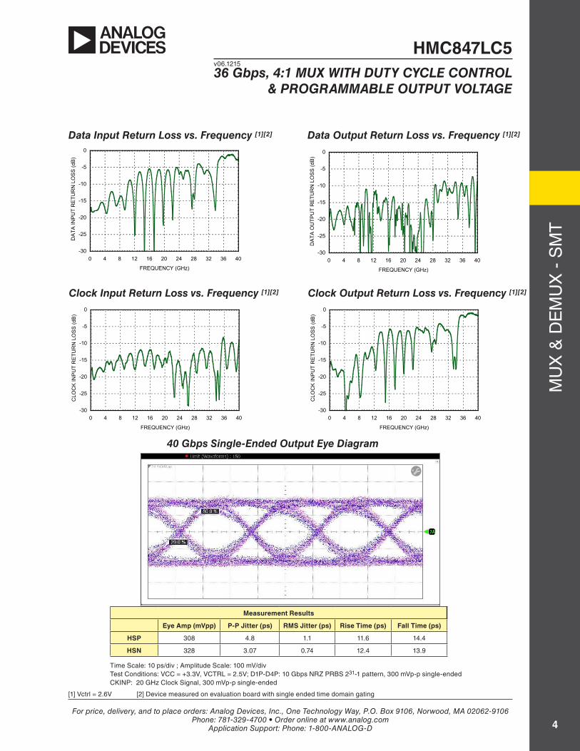
[1] Vctrl = 2.6V [2] Device measured on evaluation board with single ended time domain gating
Data Input Return Loss vs. Frequency [1][2]
Clock Input Return Loss vs. Frequency [1][2]
Data Output Return Loss vs. Frequency [1][2]
Clock Output Return Loss vs. Frequency [1][2]
40 Gbps Single-Ended Output Eye Diagram
Time Scale: 10 ps/div ; Amplitude Scale: 100 mV/divTest Conditions: VCC = +3.3V, VCTRL = 2.5V; D1P-D4P: 10 Gbps NRZ PRBS 231-1 pattern, 300 mVp-p single-endedCKINP: 20 GHz Clock Signal, 300 mVp-p single-ended
-30
-25
-20
-15
-10
-5
0
0 4 8 12 16 20 24 28 32 36 40
DAT
A IN
PUT
RET
UR
N L
OSS
(dB)
FREQUENCY (GHz)
-30
-25
-20
-15
-10
-5
0
0 4 8 12 16 20 24 28 32 36 40
CLO
CK
INP
UT
RE
TUR
N L
OS
S (d
B)
FREQUENCY (GHz)
-30
-25
-20
-15
-10
-5
0
0 4 8 12 16 20 24 28 32 36 40
DAT
A O
UTP
UT
RET
UR
N L
OSS
(dB)
FREQUENCY (GHz)
-30
-25
-20
-15
-10
-5
0
0 4 8 12 16 20 24 28 32 36 40
CLO
CK
INP
UT
RE
TUR
N L
OS
S (d
B)
FREQUENCY (GHz)
Measurement Results
Eye Amp (mVpp) P-P Jitter (ps) RMS Jitter (ps) Rise Time (ps) Fall Time (ps)
HSP 308 4.8 1.1 11.6 14.4
HSN 328 3.07 0.74 12.4 13.9

For price, delivery, and to place orders: Analog Devices, Inc., One Technology Way, P.O. Box 9106, Norwood, MA 02062-9106Phone: 781-329-4700 • Order online at www.analog.com
Application Support: Phone: 1-800-ANALOG-D
MU
X &
DE
MU
X -
SM
T
5
HMC847LC5v06.1215
36 Gbps, 4:1 MUX WITH DUTY CYCLE CONTROL & PROGRAMMABLE OUTPUT VOLTAGE
36Gbps Single-Ended Output Eye Diagram
Time Scale: 10 ps/div ; Amplitude Scale: 100 mV/divTest Conditions: VCC = +3.3V, VCTRL = 2.5V; D1P-D4P: 9 Gbps NRZ PRBS 231-1 pattern, 300 mVp-p single-endedCKINP: 18 GHz Clock Signal, 300 mVp-p single-ended
Measurement Results
Eye Amp (mVpp) P-P Jitter (ps) RMS Jitter (ps) Rise Time (ps) Fall Time (ps)
HSP 320 4.27 1.03 12.7 13.5
HSN 338 3.33 0.65 12.7 12.7
20 Gbps Single-Ended Output Eye Diagram
Time Scale: 20 ps/div ; Amplitude Scale: 100 mV/divTest Conditions: VCC = +3.3V, VCTRL = 2.5V; D1P-D4P: 5 Gbps NRZ PRBS 231-1 pattern, 300 mVp-p single-endedCKINP: 10 GHz Clock Signal, 300 mVp-p single-ended
Measurement Results
Eye Amp (mVpp) P-P Jitter (ps) RMS Jitter (ps) Rise Time (ps) Fall Time (ps)
HSP 336 2.93 0.91 14.2 15.8
HSN 352 2.13 0.73 13 14.4

For price, delivery, and to place orders: Analog Devices, Inc., One Technology Way, P.O. Box 9106, Norwood, MA 02062-9106Phone: 781-329-4700 • Order online at www.analog.com
Application Support: Phone: 1-800-ANALOG-D
MU
X &
DE
MU
X -
SM
T
6
HMC847LC5v06.1215
36 Gbps, 4:1 MUX WITH DUTY CYCLE CONTROL & PROGRAMMABLE OUTPUT VOLTAGE
Timing Diagram

For price, delivery, and to place orders: Analog Devices, Inc., One Technology Way, P.O. Box 9106, Norwood, MA 02062-9106Phone: 781-329-4700 • Order online at www.analog.com
Application Support: Phone: 1-800-ANALOG-D
MU
X &
DE
MU
X -
SM
T
7
HMC847LC5v06.1215
36 Gbps, 4:1 MUX WITH DUTY CYCLE CONTROL & PROGRAMMABLE OUTPUT VOLTAGE
Absolute Maximum Ratings
ELECTROSTATIC SENSITIVE DEVICEOBSERVE HANDLING PRECAUTIONS
Outline Drawing
Power Supply Voltage (Vcc) +0.5V to +3.7V
Input Voltages Vcc -2V to Vcc +0.5V
DC Control Pins (Vctrl, Vdcc) Vcc +0.2V to Vcc -2.5V
Channel Temperature 125 °C
Continuous Pdiss (T = 85 °C)(derate 50.91 mW/°C above 85 °C )
2.04 W
Thermal Resistance(Channel to die bottom)
19.64 °C/W
Storage Temperature -65°C to +150°C
Operating Temperature -40°C to +85°C
ESD Level (HBM) Class 1B
NOTES:1. PACKAGE BODY MATERIAL: ALUMINA2. LEAD AND GROUND PADDLE PLATING: 30-80 MICROINCHES GOLD OVER 50 MICROINCHES MINIMUM NICKEL.3. DIMENSIONS ARE IN INCHES [MILLIMETERS].4. LEAD SPACING TOLERANCE IS NON-CUMULATIVE.5. CHARACTERS TO BE BLACK INK MARKED WITH .018”MIN to .030”MAX HEIGHT REQUIREMENTS. UTILIZE MAXIMUM CHARACTER HEIGHT BASED ON LID DIMENSIONS AND BEST FIT. LOCATE APPROX. AS SHOWN.6. PACKAGE WARP SHALL NOT EXCEED 0.05mm DATUM -C-7. ALL GROUND LEADS AND GROUND PADDLE MUST BE SOLDERED TO PCB RF GROUND.
Package InformationPart Number Package Body Material Lead Finish MSL Rating [2] Package Marking [1]
HMC847LC5 Alumina, White Gold over Nickel MSL3H847XXXX
[1] 4-Digit lot number XXXX[2] Max peak reflow temperature of 260 °C

For price, delivery, and to place orders: Analog Devices, Inc., One Technology Way, P.O. Box 9106, Norwood, MA 02062-9106Phone: 781-329-4700 • Order online at www.analog.com
Application Support: Phone: 1-800-ANALOG-D
MU
X &
DE
MU
X -
SM
T
8
HMC847LC5v06.1215
36 Gbps, 4:1 MUX WITH DUTY CYCLE CONTROL & PROGRAMMABLE OUTPUT VOLTAGE
Pin Number Function Description Interface Schematic
1, 10, 16, 18, 24, 26
VCC Power Supply (3.3V)
2, 3, 5, 6, 27, 28, 30, 31
D2P, D2N, D4N, D4P, D1P, D1N,
D3N, D3PDifferential 4 Channel Serial Data Inputs.
4, 7, 12, 15, 19, 22, 25, 29, 32
GND Signal and supply ground
8, 9CKOUTN, CKOUTP
Differential Quarter Rate System Clock Outputs.
11 N/C Not connected.
13, 14 CKINN, CKINP Differential Half Rate Clock Inputs.
17 Vdcc Output Duty Cycle Correction Control
20, 21 OUTP, OUTN Differential High Speed Serial Data Outputs
Pin Descriptions
For price, delivery, and to place orders: Analog Devices, Inc., One Technology Way, P.O. Box 9106, Norwood, MA 02062-9106Phone: 781-329-4700 • Order online at www.analog.com
Application Support: Phone: 1-800-ANALOG-D
MU
X &
DE
MU
X -
SM
T
9
HMC847LC5v06.1215
36 Gbps, 4:1 MUX WITH DUTY CYCLE CONTROL & PROGRAMMABLE OUTPUT VOLTAGE
Pin Descriptions (Continued)
Pin Number Function Description Interface Schematic
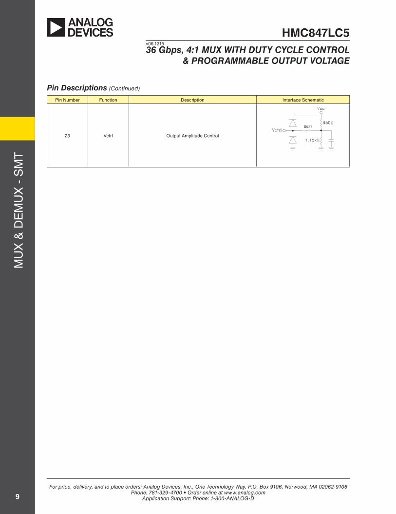
23 Vctrl Output Amplitude Control

For price, delivery, and to place orders: Analog Devices, Inc., One Technology Way, P.O. Box 9106, Norwood, MA 02062-9106Phone: 781-329-4700 • Order online at www.analog.com
Application Support: Phone: 1-800-ANALOG-D
MU
X &
DE
MU
X -
SM
T
10
HMC847LC5v06.1215
36 Gbps, 4:1 MUX WITH DUTY CYCLE CONTROL & PROGRAMMABLE OUTPUT VOLTAGE
Evaluation PCB
List of Materials for Evaluation PCB 126674 [1]
Item Description
J1, J2, J18, J19 DC Connector
J4, J7 K Connector
J5, J6 2.4mm Connector
J8 - J17 SMA Connector
C1, C19 - C25 100 nF Capacitor, 0402 Pkg.
C3 - C12 10 nF Capacitor, 0402 Pkg.
C13 - C18 1 nF Capacitor, 0201 Pkg.
C26, C28, C29 4.7 µF Capacitor, Tantalum
U1 HMC847LC5 36 Gbps 4:1 Mux
PCB [2] 126672 Evaluation Board
[1] Reference this number when ordering complete evaluation PCB
[2] Circuit Board Material: Arlon 25FR or Rogers 4350
The circuit board used in the application should use RF circuit design techniques. Signal lines should have 50 Ohm impedance while the package gro-und leads should be connected directly to the ground plane similar to that shown. The exposed metal package base must be connected to GND. A sufficient number of via holes should be used to connect the top and bottom ground planes. The evaluation circuit board shown is available from Hittite upon request.

For price, delivery, and to place orders: Analog Devices, Inc., One Technology Way, P.O. Box 9106, Norwood, MA 02062-9106Phone: 781-329-4700 • Order online at www.analog.com
Application Support: Phone: 1-800-ANALOG-D
MU
X &
DE
MU
X -
SM
T
11
HMC847LC5v06.1215
36 Gbps, 4:1 MUX WITH DUTY CYCLE CONTROL & PROGRAMMABLE OUTPUT VOLTAGE
Application Circuit