35.analog circuits for gate by r.k.kanodia
TRANSCRIPT

Eighth Edition
GATEELECTRONICS & COMMUNICATION
Analog CircuitsVol 5 of 10
RK Kanodia Ashish Murolia
NODIA & COMPANY

GATE Electronics & Communication Vol 5, 8eAnalog CircuitsRK Kanodia & Ashish Murolia
Copyright © By NODIA & COMPANY
Information contained in this book has been obtained by author, from sources believes to be reliable. However, neither NODIA & COMPANY nor its author guarantee the accuracy or completeness of any information herein, and NODIA & COMPANY nor its author shall be responsible for any error, omissions, or damages arising out of use of this information. This book is published with the understanding that NODIA & COMPANY and its author are supplying information but are not attempting to render engineering or other professional services.
MRP 660.00
NODIA & COMPANYB 8, Dhanshree Ist, Central Spine, Vidyadhar Nagar, Jaipur 302039Ph : +91 141 2101150, www.nodia.co.inemail : [email protected]
Printed by Nodia and Company, Jaipur

To Our Parents


Preface to the Series
For almost a decade, we have been receiving tremendous responses from GATE aspirants for our earlier books: GATE Multiple Choice Questions, GATE Guide, and the GATE Cloud series. Our first book, GATE Multiple Choice Questions (MCQ), was a compilation of objective questions and solutions for all subjects of GATE Electronics & Communication Engineering in one book. The idea behind the book was that Gate aspirants who had just completed or about to finish their last semester to achieve his or her B.E/B.Tech need only to practice answering questions to crack GATE. The solutions in the book were presented in such a manner that a student needs to know fundamental concepts to understand them. We assumed that students have learned enough of the fundamentals by his or her graduation. The book was a great success, but still there were a large ratio of aspirants who needed more preparatory materials beyond just problems and solutions. This large ratio mainly included average students.
Later, we perceived that many aspirants couldn’t develop a good problem solving approach in their B.E/B.Tech. Some of them lacked the fundamentals of a subject and had difficulty understanding simple solutions. Now, we have an idea to enhance our content and present two separate books for each subject: one for theory, which contains brief theory, problem solving methods, fundamental concepts, and points-to-remember. The second book is about problems, including a vast collection of problems with descriptive and step-by-step solutions that can be understood by an average student. This was the origin of GATE Guide (the theory book) and GATE Cloud (the problem bank) series: two books for each subject. GATE Guide and GATE Cloud were published in three subjects only.
Thereafter we received an immense number of emails from our readers looking for a complete study package for all subjects and a book that combines both GATE Guide and GATE Cloud. This encouraged us to present GATE Study Package (a set of 10 books: one for each subject) for GATE Electronic and Communication Engineering. Each book in this package is adequate for the purpose of qualifying GATE for an average student. Each book contains brief theory, fundamental concepts, problem solving methodology, summary of formulae, and a solved question bank. The question bank has three exercises for each chapter: 1) Theoretical MCQs, 2) Numerical MCQs, and 3) Numerical Type Questions (based on the new GATE pattern). Solutions are presented in a descriptive and step-by-step manner, which are easy to understand for all aspirants.
We believe that each book of GATE Study Package helps a student learn fundamental concepts and develop problem solving skills for a subject, which are key essentials to crack GATE. Although we have put a vigorous effort in preparing this book, some errors may have crept in. We shall appreciate and greatly acknowledge all constructive comments, criticisms, and suggestions from the users of this book. You may write to us at [email protected] and [email protected].
Acknowledgements
We would like to express our sincere thanks to all the co-authors, editors, and reviewers for their efforts in making this project successful. We would also like to thank Team NODIA for providing professional support for this project through all phases of its development. At last, we express our gratitude to God and our Family for providing moral support and motivation.
We wish you good luck ! R. K. KanodiaAshish Murolia

SYLLABUS
GATE Electronics & CommunicationsSmall Signal Equivalent circuits of diodes, BJTs, MOSFETs and analog CMOS. Simple diode circuits, clipping, clamping, rectifier. Biasing and bias stability of transistor and FET amplifiers. Amplifiers: single-and multi-stage, differential and operational, feedback, and power. Frequency response of amplifiers. Simple op-amp circuits. Filters. Sinusoidal oscillators; criterion for oscillation; single-transistor and op-amp configurations. Function generators and wave-shaping circuits, 555 Timers. Power supplies.
IES Electronics & Telecommunication
Transistor biasing and stabilization. Small signal analysis. Power amplifiers. Frequency response. Wide banding techniques. Feedback amplifiers. Tuned amplifiers. Oscillators. Rectifiers and power supplies. Op Amp, PLL, other linear integrated circuits and applications. Pulse shaping circuits and waveform generators.
**********

CONTENTS
CHAPTER 1 DIODE CIRCUITS
1.1 INTRODUCTION 1
1.2 DIODE 1
1.2.1 Operating Modes of a Diode 1
1.2.2 Current-Voltage Characteristics of a Diode 2
1.2.3 Current-Voltage Characteristics of an Ideal Diode 2
1.3 LOAD LINE ANALYSIS 3
1.4 PIECEWISE LINEAR MODEL 3
1.5 SMALL SIGNAL MODEL 4
1.5.1 Small Signal Resistance 4
1.5.2 AC and DC Equivalent Model 4
1.6 CLIPPER AND CLAMPER CIRCUITS 6
1.6.1 Clippers 6
1.6.2 Clampers 8
1.7 VOLTAGE MULTIPLIER CIRCUIT 9
1.7.1 Voltage Doubler 10
1.7.2 Voltage Tripler and Quadrupler 11
1.8 RECTIFIER CIRCUIT 11
1.8.1 Parameters of Rectifier Circuit 12
1.8.2 Classification of Rectifiers 12
1.9 HALF WAVE RECTIFIERS 12
1.10 FULL WAVE RECTIFIERS 14
1.10.1 Centre Taped Full wave Rectifier 14
1.10.2 Bridge Rectifier 15
1.11 FILTERS 15
1.12 ZENER DIODE 16
1.13 VOLTAGE REGULATORS 16
EXERCISE 1.1 18
EXERCISE 1.2 36
EXERCISE 1.3 42
SOLUTIONS 1.1 47
SOLUTIONS 1.2 90

SOLUTIONS 1.3 111
CHAPTER 2 BJT BIASING
2.1 INTRODUCTION 117
2.2 BASIC BIPOLAR JUNCTION TRANSISTOR 117
2.2.1 Simplified Structure of BJT 117
2.2.2 Operating Modes of BJT 118
2.2.3 Circuit Symbol and Conventions for a BJT 118
2.3 BJT CONFIGURATION 119
2.3.1 Common Base Configuration 119
2.3.2 Common Emitter configuration 120
2.3.3 Common-Collector Configuration 122
2.4 CURRENT RELATIONSHIPS IN BJT 122
2.4.1 Relation between Current Gain 122
2.4.2 Relation between Leakage Currents 123
2.5 LOAD LINE ANALYSIS 123
2.6 BIASING 125
2.6.1 Fixed Bias Circuit 125
2.6.2 Emitter Stabilized Bias Circuit 126
2.6.3 Voltage Divider Bias 128
2.7 BIAS STABILIZATION 129
2.7.1 Stability factor 129
2.7.2 Total Effect on the Collector Current 129
2.8 EARLY EFFECT 130
EXERCISE 2.1 132
EXERCISE 2.2 147
EXERCISE 2.3 155
SOLUTIONS 2.1 159
SOLUTIONS 2.2 201
SOLUTIONS 2.3 224
CHAPTER 3 BJT AMPLIFIERS
3.1 INTRODUCTION 229
3.2 AC LOAD LINE ANALYSIS 229
3.3 HYBRID EQUIVALENT MODEL 230
3.3.1 Current Gain 230
3.3.2 Voltage Gain 230
3.3.3 Input Impedance 231

3.3.4 Output Impedance 231
3.4 SMALL SIGNAL PARAMETER 232
3.4.1 Collector Current and the Transconductance 232
3.4.2 Base Current and Input Resistance at the Base 233
3.4.3 Emitter Current and the Input Resistance at the Emitter 233
3.5 HYBRID-p MODEL 233
3.5.1 Hybrid p-model Circuit Including the Early Effect 235
3.6 ANALYSIS OF STANDARD MODELS 235
3.6.1 Common Emitter Fixed Bias Configuration 235
3.6.2 Voltage Divider Bias 236
3.6.3 Common-Emitter Bias Configuration 237
3.7 FREQUENCY RESPONSE OF COMMON EMITTER AMPLIFIER 238
3.7.1 Cut-off Frequency 239
EXERCISE 3.1 241
EXERCISE 3.2 254
EXERCISE 3.3 260
SOLUTIONS 3.1 265
SOLUTIONS 3.2 295
SOLUTIONS 3.3 315
CHAPTER 4 FET BIASING
4.1 INTRODUCTION 321
4.2 JUNCTION FIELD EFFECT TRANSISTOR (JFET) 321
4.2.1 Circuit Symbols of JFET 321
4.2.2 Characteristics of JFET 322
4.3 METAL-OXIDE SEMICONDUCTOR FIELD EFFECT TRANSISTOR (MOSFET) 323
4.3.1 n -channel Enhancement Type MOSFET 323
4.3.2 p-channel Enhancement Type MOSFET 325
4.3.3 n -channel Depletion Type MOSFET 326
4.3.4 p-channel Depletion Type MOSFET 326
4.4 SOME STANDARD CONFIGURATIONS FOR JFET 328
4.4.1 Fixed Bias Configuration 328
4.4.2 Self Bias Configuration 329
4.4.3 Voltage Divider Biasing 330
4.5 BIASING CONFIGURATION FOR DEPLETION TYPE MOSFET’S 331
4.6 SOME STANDARD CONFIGURATIONS FOR ENHANCEMENT TYPE MOSFET CIRCUITS 331
4.6.1 Feedback Biasing Configuration 331
4.6.2 Voltage Divider Biasing Configuration 332

4.6.3 Enhancement Mode NMOS device with the Gate Connected to the Drain 333
EXERCISE 4.1 334
EXERCISE 4.2 347
EXERCISE 4.3 354
SOLUTIONS 4.1 358
SOLUTIONS 4.2 388
SOLUTIONS 4.3 408
CHAPTER 5 FET AMPLIFIERS
5.1 INTRODUCTION 413
5.2 SMALL SIGNAL ANALYSIS OF JFET CIRCUIT 413
5.2.1 Transconductance 413
5.2.2 Output Resistance 414
5.3 SOME STANDARD CONFIGURATIONS 414
5.3.1 JFET Fixed Bias Configuration 414
5.3.2 JFET Self Bias Configuration with bypassed Capacitor 415
5.3.3 JFET Self Bias Configuration with Unbypassed RS 416
5.3.4 JFET Voltage Divider Configuration 418
5.3.5 JFET Source Follower (Common Drain) Configuration 418
5.3.6 JFET Common Gate Configuration 420
5.4 SMALL SIGNAL ANALYSIS OF DEPLETION TYPE MOSFET 421
5.5 SMALL SIGNAL ANALYSIS FOR ENHANCEMENT TYPE MOSFET 422
EXERCISE 5.1 423
EXERCISE 5.2 432
EXERCISE 5.3 438
SOLUTIONS 5.1 442
SOLUTIONS 5.2 467
SOLUTIONS 5.3 483
CHAPTER 6 OUTPUT STAGES AND POWER AMPLIFIERS
6.1 INTRODUCTION 487
6.2 GENERAL CONSIDERATION 487
6.2.1 Power 487
6.2.2 Power Efficiency 487
6.3 EMITTER FOLLOWER AS POWER AMPLIFIER 487
6.3.1 Small Signal Voltage Gain of Emitter Follower 487
6.3.2 Relation between Input and Output Voltage 488
6.3.3 Emitter Follower Power Rating 488

6.3.4 Power Efficiency 489
6.4 PUSH-PULL STAGE 489
6.5 CLASSES OF AMPLIFIERS 490
6.5.1 Class-A Operation 491
6.5.2 Class-B Operation : 492
6.5.3 Class-AB Output Stage 493
6.6 AMPLIFIER DISTORTION 494
6.6.1 Total harmonic Distortion 494
6.6.2 Relationship Between Total Power and THD 494
6.7 HEAT SINKS 494
6.7.1 Junction Temperature 495
6.7.2 Thermal Resistance 495
6.7.3 Transistor Case and Heat Sink 495
EXERCISE 6.1 496
EXERCISE 6.2 508
EXERCISE 6.3 513
SOLUTIONS 6.1 517
SOLUTIONS 6.2 539
SOLUTIONS 6.3 551
CHAPTER 7 OP- AMP CHARACTERISTICS AND BASIC CIRCUITS
7.1 INTRODUCTION 555
7.2 OPERATIONAL AMPLIFIER 555
7.3 IDEAL OP-AMP CIRCUIT 555
7.3.1 Transfer Characteristic of Ideal Op-amp 556
7.3.2 Common Mode Signal for Ideal Op-amp 556
7.4 PRACTICAL OP-AMP CIRCUITS 556
7.4.1 Inverting Amplifier 556
7.4.2 Non-inverting Amplifier 558
7.4.3 Unity Follower 558
7.4.4 Summing Amplifier 558
7.4.5 Amplifier with a T -network 559
7.5 PRACTICAL OP-AMP CIRCUITS WITH FINITE GAIN 559
7.5.1 Unity Follower 560
7.5.2 Inverting Amplifier 560
7.5.3 Non-inverting Amplifier 561
7.6 SLEW RATE 561
7.6.1 Maximum Signal Frequency in terms of Slew Rate 562

7.7 DIFFERENTIAL AND COMMON-MODE OPERATION 562
7.7.1 Differential Inputs 562
7.7.2 Common Inputs 562
7.7.3 Output voltage 562
7.7.4 Common Mode Rejection Ratio (CMRR) 562
7.8 DC OFFSET PARAMETER 563
7.8.1 Output Offset Voltage due to Input Offset Voltage 563
7.8.2 Output Offset Voltage due to Input Offset Current 563
EXERCISE 7.1 565
EXERCISE 7.2 578
EXERCISE 7.3 587
SOLUTIONS 7.1 591
SOLUTIONS 7.2 619
SOLUTIONS 7.3 644
CHAPTER 8 OP - AMP APPLICATION
8.1 INTRODUCTION 649
8.2 INVERTING AMPLIFIER 649
8.3 NON-INVERTING AMPLIFIER 650
8.4 MULTIPLE-STAGE GAINS 650
8.5 VOLTAGE SUBTRACTION 650
8.6 CURRENT TO VOLTAGE CONVERTER 651
8.7 VOLTAGE TO CURRENT CONVERTER 651
8.8 DIFFERENCE AMPLIFIER 652
8.9 INSTRUMENTATION AMPLIFIER 653
8.10 INTEGRATOR 654
8.11 DIFFERENTIATOR 655
8.12 LOGARITHMIC AMPLIFIER 655
8.13 EXPONENTIAL AMPLIFIER 656
8.14 SQUARE-ROOT AMPLIFIER 656
8.15 COMPARATOR 657
8.16 SCHMITT TRIGGER 657
8.17 NON INVERTING SCHMITT TRIGGER CIRCUIT 658
8.18 PRECISION RECTIFIER 659
8.19 FUNCTION GENERATOR 660
EXERCISE 8.1 661

EXERCISE 8.2 679
EXERCISE 8.3 684
SOLUTIONS 8.1 688
SOLUTIONS 8.2 734
SOLUTIONS 8.3 751
CHAPTER 9 ACTIVE FILTERS
9.1 INTRODUCTION 757
9.2 ACTIVE FILTER 757
9.2.1 Low Pass Filter 757
9.2.2 High Pass Filter 759
9.2.3 Band pass filter 759
9.3 THE FILTER TRANSFER FUNCTION 760
9.3.1 Pole-Zero Pattern of Low Pass Filter 761
9.3.2 Pole-Zero Pattern of Band Pass Filter 761
9.3.3 First-Order Filter Transfer Function 762
9.3.4 Second-order Filter Transfer Function 763
9.4 BUTTERWORTH FILTERS 765
9.5 THE CHEBYSHEV FILTER 765
9.6 SWITCHED CAPACITOR FILTER 765
9.7 SENSITIVITY 766
EXERCISE 9.1 767
EXERCISE 9.2 778
EXERCISE 9.3 781
SOLUTIONS 9.1 786
SOLUTIONS 9.2 813
SOLUTIONS 9.3 818
CHAPTER 10 FEEDBACK AMPLIFIER AND OSCILLATOR
10.1 INTRODUCTION 821
10.2 FEEDBACK 821
10.2.1 Negative Feedback 821
10.2.2 Positive Feedback 822
10.3 THE FOUR BASIC FEEDBACK TOPOLOGIES 822
10.3.1 Voltage Amplifier 822
10.3.2 Current Amplifier 823
10.3.3 Transconductance Amplifier 823
10.3.4 Transresistance Amplifier 824

10.4 ANALYSIS OF FEEDBACK AMPLIFIER 824
10.5 OSCILLATORS 826
10.6 OP-AMP RC OSCILLATOR CIRCUITS 826
10.6.1 Wein Bridge Oscillator 826
10.6.2 Phase Shift Oscillator 827
10.7 LC OSCILLATOR CIRCUIT 827
10.7.1 Colpitts Oscillator 827
10.7.2 Hartley oscillator 828
10.8 THE 555 CIRCUIT 828
10.8.1 Monostable Multivibrator 828
10.8.2 Astable Multivibrator 829
EXERCISE 10.1 830
EXERCISE 10.2 840
EXERCISE 10.3 844
SOLUTIONS 10.1 849
SOLUTIONS 10.2 873
SOLUTIONS 10.3 878
***********

Page 15Chap 1
Diode Circuits
Page 15Chap 1
Diode Circuits
www.nodia.co.in
Buy Online: shop.nodia.co.in *Shipping Free* *Maximum Discount*
GATE STUDY PACKAGE Electronics & Communication
Sample Chapter of Analog Circuits (Vol-5, GATE Study Package)
1.1 INTRODUCTION
A general goal of this chapter is to develop the ability to use the piece wise linear model and approximation techniques in the hand analysis and design of various diode circuits. The chapter includes the following topics: • Introduction to diode
• AC and DC analysis of diode.
• Application of diodes to perform signal processing functions: rectification, clipping and clamping.
• Zener diode, which operates in the reverse breakdown region
• Application of Zener diode in voltage regulators
1.2 DIODE
Diode is a two terminal device with nonlinear i -v (current-voltage) characteristics. Figure 1.1 shows the circuit symbol of a diode. In the diode symbol, the triangular head denoting the allowable direction of current flow and the vertical bar representing the blocking behaviour for currents in the opposite direction. The corresponding terminals are called the anode (or p-terminal) and the cathode (or n -terminal) respectively.
Figure 1.1: Diode Circuit Symbol
1.2.1 Operating Modes of a Diode
A diode operates in the following two modes:1. Forward bias
2. Reverse bias
Forward Bias
If the p-terminal of a diode is at higher voltage level than the n -terminal (i.e. positive voltage applied across diode), a positive current flows through the diode. The diode, operating in this mode, is said to be turned ON or forward biased. Mathematically, we define the condition for a forward biased diode as
CHAPTER 1DIODE CIRCUITS

Page 16Chap 1Diode Circuits
Page 16Chap 1Diode Circuits
www.nodia.co.in
GATE STUDY PACKAGE Electronics & Communication
Buy Online: shop.nodia.co.in *Shipping Free* *Maximum Discount*
10 Subject-wise books by R. K. KanodiaNetworks Electronic Devices Analog Circuits
Digital Circuits Signals & Systems Control Systems ElectromagneticsCommunication SystemsGeneral Aptitude Engineering Mathematics
Forward bias
V V
V V
V V V 0
>>
>
anode cathode
p n
D p n= -
_
`
a
bb
bb
Reverse Bias
If the p-terminal of an ideal diode is at lower voltage level than the n-terminal (i.e. negative voltage applied across diode), then there is no current across the diode. The diode operating in this mode is said to be turned OFF or reverse biased. Mathematically, we define the condition for a reverse biased diode as
Reverse bias
V V
V V
V V V 0
<<
<
anode cathode
p n
D p n= -
_
`
a
bb
bb
1.2.2 Current-Voltage Characteristics of a Diode
The theoretical relationship between the voltage ( )VD and current ( )iD in the pn junction is given by
iD [ ( ) ]expI 1S VV
T
D= -h ...(1.1)where the parameter IS is the reverse saturation current, VT is thermal voltage, and h is the emission coefficient or ideality factor.
NOTE :Thermal voltage at room temperature is . VV 0 026T = . The value of ideality factor is in the range 1 2# #h . For germanium, 1h = , and for silicon, 2h = .
1.2.3 Current-Voltage Characteristics of an Ideal Diode
The ideal diode may be considered as the most fundamental non-linear circuit element. Figure 1.2 (a) and (b) shows the current-voltage characteristics of an ideal diode in the forward bias and reverse bias regions, respectively.
(a) Forward Biased Diode,
(b) Reverse Biased Diode
Figure 1.2: Current-Voltage Characteristic of (a) Forward Biased Diode, (b) Reverse Biased Diode
Combining the two graphs, we get the overall current-voltage characteristic of an ideal diode (as opposed to the i -v characteristic of a diode given in equation (1.1)) as shown in Figure 1.3.

Page 17Chap 1
Diode Circuits
Page 17Chap 1
Diode Circuits
www.nodia.co.in
Buy Online: shop.nodia.co.in *Shipping Free* *Maximum Discount*
GATE STUDY PACKAGE Electronics & Communication
Sample Chapter of Analog Circuits (Vol-5, GATE Study Package)
Figure 1.3: Current-Voltage Characteristic of an Ideal Diode
1.3 LOAD LINE ANALYSIS
The applied load to a device normally have an important impact on the point or region of operation of the device. Load line analysis is the graphical approach to analyse the operation of a circuit. Consider the network shown in Figure 1.4 (a). Applying KVL in the circuit,
E V VD R- - 0= E V I RD D= + ...(1.2)
(a) (b)
Figure 1.4: (a) A Simple Diode Circuit, (b) Load Line Characteristic for the Diode Circuit
Substituting V 0D = in equation (1.2), we have
ID RE
V 0D
==
...(1.3)
Again, substituting I 0D = in equation (1.2), we get
VD EI 0D
==
The two variables (VD , ID) are the same as the diode axis variable, so we draw the load line and determine the point of intersection, as shown in Figure 1.4 (b).
1.4 PIECEWISE LINEAR MODEL
Figure 1.5 shows the piecewise linear model of a diode forward characteristic. The exponential curve is approximated by two straight lines, line A with zero slope and line B with a slope of rd . The straight line model or piecewise linear model can be described as
ID 0= , V VD # g
ID rV V
d
D=- g , V VD $ g
where rd = Diode forward resistance
Vg = cut in voltage of diode

Page 18Chap 1Diode Circuits
Page 18Chap 1Diode Circuits
www.nodia.co.in
GATE STUDY PACKAGE Electronics & Communication
Buy Online: shop.nodia.co.in *Shipping Free* *Maximum Discount*
10 Subject-wise books by R. K. KanodiaNetworks Electronic Devices Analog Circuits
Digital Circuits Signals & Systems Control Systems ElectromagneticsCommunication SystemsGeneral Aptitude Engineering Mathematics
(a) (b)
Figure 1.5: (a) Piecewise Linear Model of the Diode Forward Characteristics, and (b) its Equivalent Circuit Representation
1.5 SMALL SIGNAL MODEL
When pn junction diode is used in a linear amplifier circuit, the time varying or ac characteristics of the diode becomes important. For these circuits, we define the small signal model of diode. For the small signal model analysis, assume that the ac signal is small compared to the dc component, so that a linear ac model can be developed from the non linear diode. The relationship between the diode current and voltage can be written as
iD I eS VV
T
D
. I eS VV v
T
DQ d
=+
where VDQ is the dc quiescent voltage and vd is the ac component. So,
iD I e eS VV
Vv
T
DQ
T
d
= ...(1.4)Since, the ac signal is small, i.e
vd V<< T
So, e /v Vd T Vv1T
d. + ...(1.5)
Substituting the above expression to equation (1.4), we get
iD I e Vv1S V
V
T
dT
DQ
= +_ ai k I Vv1DQT
d= +a k
I I Vv
( )( )
Quiescent diode currentdc bias current
AC currentsignal current
DQ DQT
d= +S S
where I I eDQ S VV
T
DQ
. is the quiescent diode current. Thus, the relationship between the ac components of the diode voltage and current is
id I Vv
DQT
d= ...(1.6)
1.5.1 Small Signal Resistance
The small signal incremental resistance of a diode is defined as
rd iv
IV
d
d
DQ
T= = [see equation (1.6)]
where VT is thermal voltage and IDQ is the quiescent diode current.
1.5.2 AC and DC Equivalent Model
In the above sections, we have already discussed the diode characteristics for ac and dc supply. Figure 1.4 (a) and (b) illustrate the equivalent dc model (bias model) and ac model (small signal model) of a diode.

Page 19Chap 1
Diode Circuits
Page 19Chap 1
Diode Circuits
www.nodia.co.in
Buy Online: shop.nodia.co.in *Shipping Free* *Maximum Discount*
GATE STUDY PACKAGE Electronics & Communication
Sample Chapter of Analog Circuits (Vol-5, GATE Study Package)
Figure 1.4 (a): Bias Model and (b): Small Signal Model of a Diode
METHODOLOGY: ANALYSIS OF SINGLE DIODE CIRCUIT
In using the piecewise linear model to the diode, the first objective is to determine the Linear region (forward bias or reverse bias) in which the diode is operating To do this, we can :Step 1: Find the input voltage conditions such that a diode is ‘ON’
(forward bias) then find the output signal for this condition.
Step 2: Find the input voltage condition such that a diode is OFF (Reverse bias) then find the output signal for this condition.
NOTE :Step 2 can be performed before step 1.
METHODOLOGY: ANALYSIS OF MULTIPLE DIODE CIRCUIT
Analyzing multidiode circuit requires determining if the individual diodes are ON or OFF. In many cases, the choice is not obvious so we must initially guess the state of each diode, then analyse the circuit to determine if we have a solution consistent with our initial guess. To do this, we may follow the steps given below.Step 1: Assume the state of a diode. If a diode is assumed ON the voltage
across the diode is assumed to be Vg . If a diode is assumed to be OFF the current through the diode is assumed to be zero.
Step 2: Analyse the linear circuit with the assumed states.
Step 3: Evaluate the resulting state of each diode. If the initial assumption were that a diode is OFF and the analysis shows that 0ID = or V VD # g then the assumption is correct if, however, the analysis actually shows thatI 0>D or V V>D g , then the initial assumption is incorrect. Similarly, if the initial assumption were that a diode is ON and the analysis shows that I 0D $ or V VD $ g , then the initial assumption is correct. If, however, the analysis shows that I 0<D or V V<D f , then the initial assumption is incorrect.
Step 4: If any initial assumption is proven incorrect then a new assumption must be made and the new linear circuit must be analysed. Step 3 must than be repeated.
NOTE :For simplification at the initial step always assume that all the diodes are OFF then find the voltage across diodes VD then follow step 3.

Page 20Chap 1Diode Circuits
Page 20Chap 1Diode Circuits
www.nodia.co.in
GATE STUDY PACKAGE Electronics & Communication
Buy Online: shop.nodia.co.in *Shipping Free* *Maximum Discount*
10 Subject-wise books by R. K. KanodiaNetworks Electronic Devices Analog Circuits
Digital Circuits Signals & Systems Control Systems ElectromagneticsCommunication SystemsGeneral Aptitude Engineering Mathematics
1.6 CLIPPER AND CLAMPER CIRCUITS
Diode can be used in wave shaping circuits that either limit or clip portion of a signal, or shift the dc voltage level. The circuits are called clippers and clampers, respectively.
1.6.1 Clippers
Clipper circuits, also called limiter circuits are used to eliminate portion of a signal that are above or below a specified level without distorting the remaining part of the alternating waveform. The simple form of diode clipper-one resistor and diode depending on the orientation of the diode the positive or negative region of the input signal is clipped OFF. There are two general categories of clippers:
1. Series clipper2. Parallel clipper.
1. Series Clipper
The series configuration is defined as one where the diode is in series with the load. Table 1.1 summarizes the output waveform of various biased and unbiased series clipper circuits for the input waveform shown in Figure 1.5.
Figure 1.5: Sinusoidal Input Waveform
Table 1.1: Series Clipper Circuits and its Output Waveform
Series Clippers Clipper Circuits Output Waveforms
Unbiased Series Clipper Using Ideal Diode

Page 21Chap 1
Diode Circuits
Page 21Chap 1
Diode Circuits
www.nodia.co.in
Buy Online: shop.nodia.co.in *Shipping Free* *Maximum Discount*
GATE STUDY PACKAGE Electronics & Communication
Sample Chapter of Analog Circuits (Vol-5, GATE Study Package)
Series Clippers Clipper Circuits Output Waveforms
Biased Series Clipper Using Ideal Diode
2. Parallel Clipper
The parallel clipper (or shunt clipper) has the diode in a branch parallel to the load. Table 1.2 summarizes the output waveform of various biased and unbiased parallel clipper circuits for the input waveform shown in Figure 1.5.
Table 1.2: Parallel Clipper Circuits and its Output Waveform
Parallel Clippers Clipper Circuits Output Waveforms
Unbiased Parallel Clippers Using Ideal Diode

Page 22Chap 1Diode Circuits
Page 22Chap 1Diode Circuits
www.nodia.co.in
GATE STUDY PACKAGE Electronics & Communication
Buy Online: shop.nodia.co.in *Shipping Free* *Maximum Discount*
10 Subject-wise books by R. K. KanodiaNetworks Electronic Devices Analog Circuits
Digital Circuits Signals & Systems Control Systems ElectromagneticsCommunication SystemsGeneral Aptitude Engineering Mathematics
Parallel Clippers Clipper Circuits Output Waveforms
Biased Parallel Clippers Using Ideal Diode
Following are some important points that must be remembered while analysing a parallel clipper circuit:
PROBLEM SOLVING TECHNIQUES IN PARALLEL CLIPPER
1. When the diode is in downward direction the signal will be transmitted below the reference voltage.
2. When the diode is in upward direction the signal will be transmitted above the reference voltage.
3. Under any circumstances - dc, ac, instantaneous values, pulses, and so on; Kirchoff’s voltage law must be satisfied.
1.6.2 Clampers
Clamping shifts the entire signal voltage by a dc level. In a steady state, the output waveform is an exact replica of the input waveform, but the output

Page 23Chap 1
Diode Circuits
Page 23Chap 1
Diode Circuits
www.nodia.co.in
Buy Online: shop.nodia.co.in *Shipping Free* *Maximum Discount*
GATE STUDY PACKAGE Electronics & Communication
Sample Chapter of Analog Circuits (Vol-5, GATE Study Package)
signal is shifted by a dc value that depends on the circuit. The network must have a capacitor, a diode, and a resistive elements but it can also employ an independent dc supply to introduce an additional shift. Figure 1.6 shows a clamper circuit and a sinusoidal input waveform.
(a) (b)
Figure 1.6: (a) Input Sinusoidal Waveform, (b) Clamper Circuit
For the positive half cycle of input waveform, diode is short and the output is zero, as shown in Figure 1.7 (a). The capacitor is charged in the positive half cycle. In the negative cycle, the diode is open and the output is
vo V V V2=- - =-Thus, we get the output waveform of the clamper as shown in Figure 1.7 (c).
(a) (b)
(c)
Figure 1.7: Equivalent Clamping Circuit for (a) Positive Half Cycle, (b) Negative Half Cycle of Input Waveform, (c) Output Waveform of Clamper Circuit
Following are some important points that must be remembered while solving a clamper circuit:
PROBLEM SOLVING TECHNIQUES IN CLAMPER CIRCUIT
1. When the diode is in downward direction the total signal will be clamped below the reference voltage.
2. When the diode is in upward direction the total signal will be clamped above the reference voltage.
1.7 VOLTAGE MULTIPLIER CIRCUIT
Voltage multiplier Circuits provide a means by which multiple dc voltages can be generated from a single ac source and power transformer. Here, we will discuss some typical voltage multiplier circuits.

Page 24Chap 1Diode Circuits
Page 24Chap 1Diode Circuits
www.nodia.co.in
GATE STUDY PACKAGE Electronics & Communication
Buy Online: shop.nodia.co.in *Shipping Free* *Maximum Discount*
10 Subject-wise books by R. K. KanodiaNetworks Electronic Devices Analog Circuits
Digital Circuits Signals & Systems Control Systems ElectromagneticsCommunication SystemsGeneral Aptitude Engineering Mathematics
1.7.1 Voltage Doubler
Voltage doubler circuits provide twice the peak voltages of the transformer secondary. Figure 1.8 shows the half wave voltage doubler circuit.
Figure 1.8: Half Wave Voltage Doubler Circuit
The output waveform of the voltage doubler can be determined by following two methods:
METHODOLOGY 1: TO ANALYSE OUTPUT OF VOLTAGE DOUBLER
Step 1: For positive voltage half cycle across the transformer secondary, diode D1 conducts so capacitor C1 will be charged.
Step 2: For negative voltage half cycle across the transformer secondary, diode D2 will conduct and capacitor C2 will be charged.
Step 3: Applying KVL in loop 1, we get
V V vm m o- - - 0= vo V2 m=-
METHODOLOGY 2: TO ANALYSE OUTPUT OF VOLTAGE DOUBLER
Step 1: For the given voltage doubler circuit, we deduce that it includes a negative clamper and a peak detector.

Page 25Chap 1
Diode Circuits
Page 25Chap 1
Diode Circuits
www.nodia.co.in
Buy Online: shop.nodia.co.in *Shipping Free* *Maximum Discount*
GATE STUDY PACKAGE Electronics & Communication
Sample Chapter of Analog Circuits (Vol-5, GATE Study Package)
Step 2: For the negative clamper (diode is in downward direction), the total signal will be clamped below the reference voltage, i.e.
( )v clampero V vm i=- -Step 3: Since, the peak detector provides the peak voltage at output, so
we get
vo V2 m=-
NOTE :If a circuit includes a diode and a capacitor, then the circuit is either a clamper or a peak detector. For a clamper, output is always across diode; whereas for a peak detector, output is across capacitor.
1.7.2 Voltage Tripler and Quadrupler
Figure 1.9 shows the voltage tripler and quadrupler. It is an extension of the half wave voltage doubler, which develops three and four times the peak input voltage. For positive half cycle D1 and D3 will conduct so capacitor C1, C3, C2 will be charged. For negative half cycle D2 and D4 will conduct.
Figure 1.9: Votage Tripler and Quadrupler
1.8 RECTIFIER CIRCUIT
Rectification is the process of converting an alternating voltage into one that is limited to one polarity. The diode is useful for this function because of its nonlinear characteristic that is current exists for one voltage polarity, but is essentially zero for the opposite polarity. The block diagram of a rectifier circuit is shown in Figure 1.10.
Figure 1.10: Block diagram of an electronic power supply

Page 26Chap 1Diode Circuits
Page 26Chap 1Diode Circuits
www.nodia.co.in
GATE STUDY PACKAGE Electronics & Communication
Buy Online: shop.nodia.co.in *Shipping Free* *Maximum Discount*
10 Subject-wise books by R. K. KanodiaNetworks Electronic Devices Analog Circuits
Digital Circuits Signals & Systems Control Systems ElectromagneticsCommunication SystemsGeneral Aptitude Engineering Mathematics
1.8.1 Parameters of Rectifier Circuit
Some important parameters for rectifier are described in the following texts:1. DC load current: The dc load current of a rectifier is given by
Idc area under curve output waveformof
2p =
( )I d t21
0
2
p w=p
#
2. DC load voltage: If the rectifier is terminated to load RL , then the dc load voltage of the rectifier is given by
Vdc I Rdc L=3. RMS load current: The rms load current of a rectifier is defined as
Irms I d t21 2
0
2
p w=p
^ h#4. RMS load voltage: The rms load voltage of a rectifier is given by
Vrms I Rrms L=
5. Ripple: The time dependent component present in the output of the rectifier filter is known as ripple.
6. Ripple factor: The ripple factor of a rectifier is obtained as
. .r f averge value of output currentrms value of alternating component in output current=
( )
II I
dc
rms dc2 2
=-^ h
II 1
dc
rms2
= -b l
7. Voltage regulation: The percentage voltage regulation for a rectifier is defined as
%VR ( )
( ) ( )V
V VFL
NL FL
dc
dc dc= -
where ( )V FLdc is the full load dc voltage and ( )V NLdc is the null load voltage. Ideally VR should be zero.
8. Rectifier efficiency: The rectifier efficiency is defined as
h AC input powerDC power delivered to the load= P
Pac
dc=
9. Peak inverse voltage: It is the maximum reverse bias voltage across the diode where the diode withstand.
1.8.2 Classification of Rectifiers
Rectifier circuits can be classified as1. Half wave rectifier
2. Full wave rectifier
In the following sections, we will discuss some typical classes of rectifiers.
1.9 HALF WAVE RECTIFIERS
For a half wave rectifier, the output voltage appears only during the half cycle of the input signal. Figure 1.11 shows a half wave rectifier, its input waveform, and the corresponding output waveform.

Page 27Chap 1
Diode Circuits
Page 27Chap 1
Diode Circuits
www.nodia.co.in
Buy Online: shop.nodia.co.in *Shipping Free* *Maximum Discount*
GATE STUDY PACKAGE Electronics & Communication
Sample Chapter of Analog Circuits (Vol-5, GATE Study Package)
(a)
(b) (c)
Figure 1.11: (a) Half Wave Rectifier Circuit, (b) Input Waveform, and (c) Output Waveform
Some important parameters for a half wave rectifier are described in the following table.
Table 1.3: Parameters of a Half Wave Rectifier Circuit
S.N. Parameters Expression
1. DC load current Idc Im
p=
2. DC load voltage Vdc
RR R
V
1L
f S
m
p= + +c m
where RL is load resistance, RS is second transformer resistance, and Rf is forward resistance of diode.
3. Null load dc voltage V NLdc^ h Vm
p=
if RL 3= , i.e. load terminal is open4. RMS load current Irms
I2m=
5. RMS load voltage Vrms V2m=
6. Ripple factor . .r f 1.21=
7. Voltage regulation Ideally VR should be zero, i.e. %VR 0=
8. Rectifier efficiency h .40 6.
9. Peak inverse voltage In half wave rectifier, the PIV rating of the diode must equal or exceed the peak value of the applied voltage, i.e. PIV Vm$
10. Output frequency f , i.e. same as input frequency

Page 28Chap 1Diode Circuits
Page 28Chap 1Diode Circuits
www.nodia.co.in
GATE STUDY PACKAGE Electronics & Communication
Buy Online: shop.nodia.co.in *Shipping Free* *Maximum Discount*
10 Subject-wise books by R. K. KanodiaNetworks Electronic Devices Analog Circuits
Digital Circuits Signals & Systems Control Systems ElectromagneticsCommunication SystemsGeneral Aptitude Engineering Mathematics
1.10 FULL WAVE RECTIFIERS
The full wave rectifier inverts the negative portions of the sine wave so that a unipolar output signal is generated during both halves of the input sinusoidal. Following are the full wave rectification methods:1. Centre tap full wave rectifier
2. The Bridge rectifier
1.10.1 Centre Taped Full wave Rectifier
One possible implementation of full wave rectifier is centre taped full wave rectifier. Figure 1.13 shows a centre taped full wave rectifier, input waveform, and the corresponding output waveform. The current through the two diodes in the circuit is given by
I1 sinI tm w= , t0 < <w p I2 sinI tm w= , t 2< <p w p
(a)
(b) (c)
Figure 1.13: (a) Full Wave Rectifier, (b) Input Waveform, and (c) Output Waveform
Some important parameters for a centre taped full wave rectifier are summarized in the following table.
Table 1.4: Parameters of Centre Taped Full Wave Rectifier
S.N. Parameters Expression
1. DC load current Idc I2 m
p =
3. Null load dc voltage V V2NLdc
m
p =^ h if RL 3= , i.e. load terminal is open
4. RMS load current Irms I2m=
5. RMS load voltage Vrms V
2m=
6. Ripple factor . .r f .0 48=
8. Rectifier efficiency h . %81 2.
9. Peak inverse voltage PIV V2 m=
10. Output frequency f2 , where f is the input frequency.

Page 29Chap 1
Diode Circuits
Page 29Chap 1
Diode Circuits
www.nodia.co.in
Buy Online: shop.nodia.co.in *Shipping Free* *Maximum Discount*
GATE STUDY PACKAGE Electronics & Communication
Sample Chapter of Analog Circuits (Vol-5, GATE Study Package)
1.10.2 Bridge Rectifier
An alternative implementation of the full wave rectifier is bridge rectifier. Figure 1.14 shows a bridge rectifier, input waveform, and the corresponding output waveform.
(a)
(b) (c)
Figure 1.14: (a) Bridge Rectifier, (b) Input Waveform, (c) Output Waveform
Some important parameters for a bridge rectifier are summarized in the table below.
S.N. Parameters Expression
1. DC load current Idc I2 m
p =
3. Null load dc voltage V NLdc^ h V2 m
p =
if RL 3= , i.e. load terminal is open4. RMS load current Irms
I2m=
5. RMS load voltage Vrms V
2m=
6. Ripple factor . .r f .0 48=
8. Rectifier efficiency h . %81 2.
9. Peak inverse voltage PIV Vm=
10. Output frequency f2 , where f is the input frequency.
1.11 FILTERS
A capacitor is added in parallel with the load resistor of a half wave rectifier to form a simple filter circuit as shown in fig 1.15.
Conduction Interval
The diode only conducts for a short time TT during each cycle. This time is called the conduction interval.

Page 30Chap 1Diode Circuits
Page 30Chap 1Diode Circuits
www.nodia.co.in
GATE STUDY PACKAGE Electronics & Communication
Buy Online: shop.nodia.co.in *Shipping Free* *Maximum Discount*
10 Subject-wise books by R. K. KanodiaNetworks Electronic Devices Analog Circuits
Digital Circuits Signals & Systems Control Systems ElectromagneticsCommunication SystemsGeneral Aptitude Engineering Mathematics
Output Voltage
During the discharge period the voltage across the capacitor is described by
v to ^ h V e /m
t RC= -
At the end of discharge interval, we have the output
VL V e /m
T RC= - l
where Tl is the discharge time.
(a) (b)
Figure 1.15: (a) Capacitor Filter Circuit, (b) Input and Output Waveform for the Filter
Ripple Voltage
The output voltage is no longer constant as in the ideal peak detector circuit but has ripple voltage Vr^ h. The ripple voltage is defined as the difference between Vm and VL , i.e.
Vr V V V e1 /m L m
T RC= - = - - l^ h
Since, RC T>> l, so we may write
Vr V RCT
m. lb l
or Vr V RCT
m. (T T.l )
or Vr fRCVm= ( /f T1= )
1.12 ZENER DIODE
Zener diodes are designed to provide a specified breakdown voltage. The breakdown voltage of the zener diode is nearly constant over a wide range of reverse bias currents. This makes the zener diode useful in a voltage regulator, or a constant voltage reference circuit. Figure 1.16 shows the zener diode and its equivalent circuit models for ON and OFF states.
(a) (b)
Figure 1.16: Equivalent Circuit Model for a Zener Diode for (a) ON State and (b) OFF State
1.13 VOLTAGE REGULATORS
A Voltage regulator is a device or combination of devices designed to maintain the output voltage of a power supply as nearly constant as possible. One of

Page 31Chap 1
Diode Circuits
Page 31Chap 1
Diode Circuits
www.nodia.co.in
Buy Online: shop.nodia.co.in *Shipping Free* *Maximum Discount*
GATE STUDY PACKAGE Electronics & Communication
Sample Chapter of Analog Circuits (Vol-5, GATE Study Package)
the simplest discrete Regulator consists of only a resistor and a zener diode, as shown in Figure 1.17.
Figure 1.17: Basic Zener Regulator
METHODOLOGY: TO ANALYSE ZENER REGULATOR CIRCUIT
The applied dc voltage is fixed, as is the load resistor. The zener regulator can be analysed in the following steps.Step 1: Remove the zener diode from the network.
Step 2: Calculate the voltage across the resulting open circuit.
V V R RR vL
L
Li= = +
Step 3: Determine the state of the zener diode by checking the obtained value of voltage V for the following conditions
If V Vz$ , the zener diode is ON
If V V< z , the diode is OFFStep 4: Substitute the appropriate equivalent circuit for the resulting
state of zener diode. For ON state, equivalent mode of Figure 1.16(a) can be substituted, while for OFF state the open circuit equivalence of Figure 1.16(b) is substituted.
Step 5: Solve the resulting equivalent circuit for the desired unknowns. For example, assume that the equivalent circuit for the zener regulator is as shown below.
So, we get the various parameters for the circuit as
Load voltage, VL Vz=
Load current, IL RVL=
Current through resistance R , IR RV
RV VR i L= = -
Zener current, Iz I IR L= - Power dissipated by Zener diode, Pz V Iz z=
***********

Page 32Chap 1Diode Circuits
Page 32Chap 1Diode Circuits
www.nodia.co.in
GATE STUDY PACKAGE Electronics & Communication
Buy Online: shop.nodia.co.in *Shipping Free* *Maximum Discount*
10 Subject-wise books by R. K. KanodiaNetworks Electronic Devices Analog Circuits
Digital Circuits Signals & Systems Control Systems ElectromagneticsCommunication SystemsGeneral Aptitude Engineering Mathematics
EXERCISE 1.1
MCQ 1.1.1 Consider the given circuit and a waveform for the input voltage, shown in figure below. The diode in circuit has cutin voltage 0V =g .
The waveform of output voltage vo is
MCQ 1.1.2 Consider the given circuit and a waveform for the input voltage, shown in figure below. The diode in circuit has cutin voltage 0V =g .
The waveform of output voltage vo is
MCQ 1.1.3 Consider the given circuit and a waveform for the input voltage, shown in figure below. The diode in circuit has cutin voltage 0V =g .

Page 33Chap 1
Diode Circuits
Page 33Chap 1
Diode Circuits
www.nodia.co.in
Buy Online: shop.nodia.co.in *Shipping Free* *Maximum Discount*
GATE STUDY PACKAGE Electronics & Communication
Sample Chapter of Analog Circuits (Vol-5, GATE Study Package)
The waveform of output voltage vo is
MCQ 1.1.4 Consider the given circuit and a waveform for the input voltage. The diode in circuit has cutin voltage 0V =g .
The waveform of output voltage vo is
MCQ 1.1.5 For the circuit shown below, let cut in voltage 0.7V =g V.
The plot of vo verses vi for 10 10vi# #- V is

Page 34Chap 1Diode Circuits
Page 34Chap 1Diode Circuits
www.nodia.co.in
GATE STUDY PACKAGE Electronics & Communication
Buy Online: shop.nodia.co.in *Shipping Free* *Maximum Discount*
10 Subject-wise books by R. K. KanodiaNetworks Electronic Devices Analog Circuits
Digital Circuits Signals & Systems Control Systems ElectromagneticsCommunication SystemsGeneral Aptitude Engineering Mathematics
MCQ 1.1.6 For the circuit shown below the cutin voltage of diode is 0.7V =g V.
The plot of vo versus vi is
MCQ 1.1.7 For the circuit shown below each diode has 0.7V =g V.
The vo for 10 10vs# #- V is

Page 35Chap 1
Diode Circuits
Page 35Chap 1
Diode Circuits
www.nodia.co.in
Buy Online: shop.nodia.co.in *Shipping Free* *Maximum Discount*
GATE STUDY PACKAGE Electronics & Communication
Sample Chapter of Analog Circuits (Vol-5, GATE Study Package)
MCQ 1.1.8 A symmetrical 5 kHz square wave whose output varies between 10 V+ and 10 V- is impressed upon the clipping shown in figure below
If diode has 0rf = and 2rr = MW and 0V =g , the output waveform is
MCQ 1.1.9 In the circuit shown below, the three signals of fig are impressed on the input terminals.
If diode are ideal then the voltage vo is

Page 36Chap 1Diode Circuits
Page 36Chap 1Diode Circuits
www.nodia.co.in
GATE STUDY PACKAGE Electronics & Communication
Buy Online: shop.nodia.co.in *Shipping Free* *Maximum Discount*
10 Subject-wise books by R. K. KanodiaNetworks Electronic Devices Analog Circuits
Digital Circuits Signals & Systems Control Systems ElectromagneticsCommunication SystemsGeneral Aptitude Engineering Mathematics
MCQ 1.1.10 For the circuit shown below the input voltage vi is as shown in figure.
Assume the RC time constant large and cutin voltage of diode 0V =g . The output voltage vo is
MCQ 1.1.11 For the circuit shown below, the input voltage vi is as shown in figure.
Assume the RC time constant large and cutin voltage 0V =g . The output voltage vo is

Page 37Chap 1
Diode Circuits
Page 37Chap 1
Diode Circuits
www.nodia.co.in
Buy Online: shop.nodia.co.in *Shipping Free* *Maximum Discount*
GATE STUDY PACKAGE Electronics & Communication
Sample Chapter of Analog Circuits (Vol-5, GATE Study Package)
MCQ 1.1.12 In the circuit I is DC current and capacitors are very large. Using small signal model which of following is correct ?
(A) v v V IRV
o sT s
T
hh= + (B) v vo s=
(C) v V IRv
oT S
s
h= + (D) 0vo =
Common Data For Q. 13 to 15 :Consider the circuit shown below. Assume diodes are ideal.
MCQ 1.1.13 If 10v1 = V and 5v2 = V, then output voltage vo is(A) 9 V (B) 9.474 V
(C) 0 V (D) 8.943 V
MCQ 1.1.14 If 10v v1 2= = V, then output voltage vo is(A) 9 V (B) 9.474 V
(C) 4 V (D) 8.943 V
MCQ 1.1.15 If 5v1 =- V and 5v2 = V then vo is(A) 9.474 V (B) 8.943 V
(C) 4.5 V (D) 9 V
Common Data For Q.16 and 17 :Consider the circuit shown below. Assume diodes are ideal.

Page 38Chap 1Diode Circuits
Page 38Chap 1Diode Circuits
www.nodia.co.in
GATE STUDY PACKAGE Electronics & Communication
Buy Online: shop.nodia.co.in *Shipping Free* *Maximum Discount*
10 Subject-wise books by R. K. KanodiaNetworks Electronic Devices Analog Circuits
Digital Circuits Signals & Systems Control Systems ElectromagneticsCommunication SystemsGeneral Aptitude Engineering Mathematics
MCQ 1.1.16 If 10v v1 2= = V, then output voltage vo is(A) 0 V (B) 9.737 V
(B) 9 V (D) 9.5 V
MCQ 1.1.17 If 5v1 =- V and 10v2 = V, the output voltage vo is(A) 9 V (B) 9.737 V
(C) 9.5 V (D) 4.5 V
MCQ 1.1.18 In the circuit shown below diodes has cutin voltage of 0.6 V. The diode in ON state are
(A) only D1 (B) only D2
(C) both D1 and D2 (D) None of these
MCQ 1.1.19 For the circuit shown below cutin voltage of diode is 0.7V =g . What is the value of v and i ?
(A) 2.3 V, 2.65 mA (B) 2.65 V, 2.3 mA
(C) 2 V, 0 mA (D) 0 V, 2.3 mA
MCQ 1.1.20 For the circuit shown below the value of v and i are (if the diode is ideal)
(A) 5+ V, 0 mA (B) 1+ V, 0.6 mA
(C) 5+ V, 0.4 mA (D) 1+ V, 0.4 mA
MCQ 1.1.21 For the circuit shown below each diode has 0.6V =g V and 0rf = . Both diode will be ON if

Page 39Chap 1
Diode Circuits
Page 39Chap 1
Diode Circuits
www.nodia.co.in
Buy Online: shop.nodia.co.in *Shipping Free* *Maximum Discount*
GATE STUDY PACKAGE Electronics & Communication
Sample Chapter of Analog Circuits (Vol-5, GATE Study Package)
(A) 3.9v >s V (B) 4.9v >s V
(C) 6.3v >s V (D) 5.3v >s V
Common Data For Q. 22 and 23 :The diode In the circuit shown below has the non linear terminal characteristic as shown in figure. Let the voltage be cosv ti w= V.
MCQ 1.1.22 The current iD is(A) 2.5(1 )cos tw+ mA (B) 5(0.5 )cos tw+ mA
(C) 5(1 )cos tw+ mA (D) 5(1 0.5 )cos tw+ mA
MCQ 1.1.23 The voltage vD is (A) 0.25(3 )cos tw+ V
(B) 0.25(1 3 )cos tw+ V
(C) 0.5(3 1 )cos tw+ V
(D) 0.5(2 3 )cos tw+ V
MCQ 1.1.24 The circuit inside the box in figure shown below contains only resistor and diodes. The terminal voltage vo is connected to some point in the circuit inside the box.
The largest and smallest possible value of vo most nearly to is respectively(A) 15 V, 6 V
(B) 24 V, 0 V
(C) 24 V, 6 V
(D) 15 V, 9- V
MCQ 1.1.25 The Q -point for the Zener diode shown below is
(A) (0.34 mA, 4 V)
(B) (0.34 mA, 4.93 V)
(C) (0.94 mA, 4 V)
(D) (0.94 mA, 4.93 V)

Page 40Chap 1Diode Circuits
Page 40Chap 1Diode Circuits
www.nodia.co.in
GATE STUDY PACKAGE Electronics & Communication
Buy Online: shop.nodia.co.in *Shipping Free* *Maximum Discount*
10 Subject-wise books by R. K. KanodiaNetworks Electronic Devices Analog Circuits
Digital Circuits Signals & Systems Control Systems ElectromagneticsCommunication SystemsGeneral Aptitude Engineering Mathematics
Common Data For Q. 26 to 28 :In the voltage regulator circuit shown below the zener diode current is to be limited to the range 5 100iz# # mA.
MCQ 1.1.26 The range of possible load current is(A) 5 130iL# # mA
(B) 25 120iL# # mA
(C) 10 110iL# # mA
(D) None of the above
MCQ 1.1.27 The range of possible load resistance is(A) 60 372RL# # W
(B) 60 200RL# # W(C) 40 192RL# # W
(D) 40 360RL# # W
MCQ 1.1.28 The power rating required for the load resistor is(A) 576 mW (B) 360 Wm(C) 480 mW (D) 75 Wm
MCQ 1.1.29 A clipper circuit is shown below.
Assuming forward voltage drops of the diodes to be 0.7 V, the input-output transfer characteristics of the circuit is

Page 41Chap 1
Diode Circuits
Page 41Chap 1
Diode Circuits
www.nodia.co.in
Buy Online: shop.nodia.co.in *Shipping Free* *Maximum Discount*
GATE STUDY PACKAGE Electronics & Communication
Sample Chapter of Analog Circuits (Vol-5, GATE Study Package)
MCQ 1.1.30 The following circuit has a source voltage Vs as shown in the graph. The current through the circuit is also shown.
The element connected between a and b could be
MCQ 1.1.31 In the voltage doubler circuit shown in the figure, the switch ‘S ’ is closed at t 0= . Assuming diodes D1 and D2 to be ideal, load resistance to be infinite and initial capacitor voltages to be zero. The steady state voltage across capacitor C1 and C2 will be
(A) 10 , 5V VV Vc c1 2= =
(B) 10 , 5V VV Vc c1 2= =-(C) 5 , 10V VV Vc c1 2= =
(D) 5 , 10V VV Vc c1 2= =-
MCQ 1.1.32 What are the states of the three ideal diodes of the circuit shown in figure ?
(A) , ,D D DON OFF OFF1 2 3
(B) , ,D D DOFF ON OFF1 2 3
(C) , ,D D DON OFF ON1 2 3
(D) , ,D D DOFF ON ON1 2 3

Page 42Chap 1Diode Circuits
Page 42Chap 1Diode Circuits
www.nodia.co.in
GATE STUDY PACKAGE Electronics & Communication
Buy Online: shop.nodia.co.in *Shipping Free* *Maximum Discount*
10 Subject-wise books by R. K. KanodiaNetworks Electronic Devices Analog Circuits
Digital Circuits Signals & Systems Control Systems ElectromagneticsCommunication SystemsGeneral Aptitude Engineering Mathematics
MCQ 1.1.33 The equivalent circuit of a diode, during forward biased and reverse biased conditions, are shown in the figure.
(I)
(II)
If such a diode is used in clipper circuit of figure given above, the output voltage Vo of the circuit will be
MCQ 1.1.34 Assuming the diodes D1 and D2 of the circuit shown in figure to be ideal ones, the transfer characteristics of the circuit will be

Page 43Chap 1
Diode Circuits
Page 43Chap 1
Diode Circuits
www.nodia.co.in
Buy Online: shop.nodia.co.in *Shipping Free* *Maximum Discount*
GATE STUDY PACKAGE Electronics & Communication
Sample Chapter of Analog Circuits (Vol-5, GATE Study Package)
MCQ 1.1.35 A voltage signal sin t10 w is applied to the circuit with ideal diodes, as shown in figure, The maximum, and minimum values of the output waveform Vout of the circuit are respectively
(A) 10 V+ and 10 V-
(B) 4 V+ and 4 V-(C) 7 V+ and 4 V-
(D) 4 V+ and 7 V-
MCQ 1.1.36 The forward resistance of the diode shown in Figure is 5 W and the remaining parameters are same at those of an ideal diode. The dc component of the source current is
(A) V50
m
p (B) V
50 2m
p
(C) V100 2
m
p (D) V
502 m
p
MCQ 1.1.37 The cut-in voltage of both zener diode DZ and diode D shown in Figure is 0.7 V, while break-down voltage of DZ is 3.3 V and reverse break-down voltage of D is 50 V. The other parameters can be assumed to be the same as those of an ideal diode. The values of the peak output voltage ( )Vo are
(A) 3.3 V in the positive half cycle and 1.4 V in the negative half cycle.
(B) 4 V in the positive half cycle and 5 V in the negative half cycle.
(C) 3.3 V in both positive and negative half cycles.
(D) 4 V in both positive and negative half cycle
Common Data For Q. 38 and 39In the circuit shown in Figure, the source I is a dc current source. The switch S is operated with a time period T and a duty ratio D . You may assume that the capacitance C has a finite value which is large enough so that the voltage. VC
has negligible ripple, calculate the following under steady state conditions, in terms of D , I and R

Page 44Chap 1Diode Circuits
Page 44Chap 1Diode Circuits
www.nodia.co.in
GATE STUDY PACKAGE Electronics & Communication
Buy Online: shop.nodia.co.in *Shipping Free* *Maximum Discount*
10 Subject-wise books by R. K. KanodiaNetworks Electronic Devices Analog Circuits
Digital Circuits Signals & Systems Control Systems ElectromagneticsCommunication SystemsGeneral Aptitude Engineering Mathematics
MCQ 1.1.38 The voltage Vc , with the polarity shown in Figure,
(A)CI (B) ( )C
I DT1 -
(C) ( )CI D T1 - (D) C
I T-
MCQ 1.1.39 The average output voltage Vo , with the polarity shown in figure
(A) CI T- (B) C
I D T22-
(C) ( )CI DT2 1 - (D) (1 )C
I D T2 -
Common Data For Q. 40 and 41:Consider the given circuit and the cut in voltage of each diode is 0.6 VV =g .
MCQ 1.1.40 What is the value of ID1, ID2, ID3 respectively?(A) 1.94 mA, 0.94 mA- , 1.86 mA (B) 1.47 mA, 0.94 mA, 0 mA
(C) 1.47 mA, 0 mA, 0.94 mA (D) 1.94 mA, 0 mA, 0.94 mA
MCQ 1.1.41 The value of VD1, VD2, VD3 respectively is(A) 0.6, .4 10- , 0.6 (B) 0.6, .8 8- , 0.6
(C) 0.6, 0.6, 0.6 (D) 0.6, 0.6, .4 10-
MCQ 1.1.42 The voltage regulator shown below, what are the nominal and worst case values of zener diode current if the power supply voltage, zener break down voltage and registor all have 5 % tolerance?
I nomz I nom
z I minworstz^ h
(A) 1.2 mA 0 mA 0 mA
(B) 0.5 mA 0.70 mA 0.103 mA
(C) 0.5 mA 0.60 mA 0.346 mA
(D) 0.5 mA 0.796 mA 0.215 mA
JAEGER/120/3.9
JAEGER/120/3.9
JAEGER/168/3.82

Page 45Chap 1
Diode Circuits
Page 45Chap 1
Diode Circuits
www.nodia.co.in
Buy Online: shop.nodia.co.in *Shipping Free* *Maximum Discount*
GATE STUDY PACKAGE Electronics & Communication
Sample Chapter of Analog Circuits (Vol-5, GATE Study Package)
MCQ 1.1.43 What are the nominal and worst case values of zener power dissipation?(A) 10.8 mW, 0 mW, 0 mW (B) 4.5 mW, 7.52 nW, 1.80 mW
(C) 4.5 mW, 6.81 mW, 2.03 mW (D) 4.5 mW, 5.13 mW, 5.67 mW
MCQ 1.1.44 The diode circuit in figure shown below the biasing of the diode D1, D2 is
(A) ON, ON (B) ON, OFF
(C) OFF, ON (D) OFF, OFF
MCQ 1.1.45 The diode circuit shown in figure. Assume that diode is ideal, what will be the biasing modes of diode D1, D2 and D3? (FB " forward biased, RB " reverse biased)
D1 D2 D3
(A) FB FB FB(B) FB FB RB(C) FB RB RB(D) FB RB FB
MCQ 1.1.46 The diode in the circuit shown below have linear parameter of .V 0 7=g (for Si), .V 0 3=g (for Ge) and r 0f = for both the diode. What is the biasing condition of diode D1 and D2?
(A) OND1 - , OND2 - (B) OND1 - , OFFD2 -(C) OFFD1 - , OND2 - (D) OFFD1 - , OFFD2 -
BOYL-STEAD/68/2.14

Page 46Chap 1Diode Circuits
Page 46Chap 1Diode Circuits
www.nodia.co.in
GATE STUDY PACKAGE Electronics & Communication
Buy Online: shop.nodia.co.in *Shipping Free* *Maximum Discount*
10 Subject-wise books by R. K. KanodiaNetworks Electronic Devices Analog Circuits
Digital Circuits Signals & Systems Control Systems ElectromagneticsCommunication SystemsGeneral Aptitude Engineering Mathematics
MCQ 1.1.47 In the voltage regulator circuit below rating of zener diode is given, then the range of values of vi that will maintain the zener diode in the ‘ON’ state is
(A) 16.87 36.87 Vvi1 1
(B) 16.87 23.67 Vvi1 1
(C) 23.67 36.87 Vvi1 1
(D) None of the above
MCQ 1.1.48 Consider the given a circuit and a waveform for the input voltage.
If the diode has cut in voltage V 0=g , the output waveform of the circuit is
MCQ 1.1.49 Assume that the diode cut in voltage for the circuit shown below is 0.7VV =g
. Which of clamper circuit perform the function shown below ?
BOYL-STEAD/109/29
BOYL-STEAD/112/41

Page 47Chap 1
Diode Circuits
Page 47Chap 1
Diode Circuits
www.nodia.co.in
Buy Online: shop.nodia.co.in *Shipping Free* *Maximum Discount*
GATE STUDY PACKAGE Electronics & Communication
Sample Chapter of Analog Circuits (Vol-5, GATE Study Package)
MCQ 1.1.50 Having lost his 2.4 V cellphone charger, an electrical engineering student tries several stores but does not find adaptors with outputs less than 3 V. He then decides to put his knowledge of electronics to work and constructs the circuit shown in figure where three identical diodes in forward bias produce a total voltage of 3 2.4 VV Vout D -= and resistor R1 sustain remaining voltage. Neglect the current drawn by the cellphone and assume 26 mVVThermal = . The reverse saturation current IS for the diode is
(A) 6 mA (B) 2.602 10 A16#
-
(C) 8.672 10 A14#
- (D) 7.598 10 A14#
-
Common Data For Q. 25 to 27:The circuit diagram of a zener regulator is shown in figure below. The data sheet specification for zener IN4742A provides following values
12 VVz = at 21 mAIzT = , R 9z = (assume constant) 76 mAIzM = , 1 mAIzk =.
MCQ 1.1.51 The values of zener diode voltages V maxz^ h , V minz^ h respectively are
(A) 11.82 V, 12.5 V
(B) 12.5 V, 11.82 V
(C) 12.18 V, 11.82 V
(D) 12.5 V, 11.5 V
MCQ 1.1.52 The maximum value of load current over which the zener diode is in ON state.(A) 36.88 mA (B) 35.88 mA
(C) 36.36 mA (D) 35.36 mA
MCQ 1.1.53 The value of RL (Load resistance) corresponding to maximum load current is(A) 329.43 W (B) 334.44 W(C) 325.37 W (D) 320.49 W
DESH-PANDE/169/3.17

Page 48Chap 1Diode Circuits
Page 48Chap 1Diode Circuits
www.nodia.co.in
GATE STUDY PACKAGE Electronics & Communication
Buy Online: shop.nodia.co.in *Shipping Free* *Maximum Discount*
10 Subject-wise books by R. K. KanodiaNetworks Electronic Devices Analog Circuits
Digital Circuits Signals & Systems Control Systems ElectromagneticsCommunication SystemsGeneral Aptitude Engineering Mathematics
Common Data For Q. 54 and 55 :A breakdown diode has 6.2 VVz = at 25 Cc and 0.02%/ Cz ca = . A silicon diode with 0.7 VVF = and a temperature coefficient of . /mV C1 8 c- is connected in series with the breakdown diode.
MCQ 1.1.54 The new value of reference voltage and the temperature coefficient of the series combination of diode D and zener diode.
(A) 6.9 V, 0.008 %/ Cc- (B) 6.9 V, 0.0289 %/ Cc-(C) 6.9 V, 0.0 %/ C56 c- (D) 6.2 V, 0.056 %/ Cc-
MCQ 1.1.55 The new value of Vref at a temperature of C50c is(A) 6.186 (B) 6.886 V
(C) 6.914 V (D) 6.700 V
MCQ 1.1.56 The diode circuit given below. Assume diode is ideal. The operating states of diodes D1, D2 are
D1 D2
(A) ON, ON(B) ON, OFF(C) OFF, ON(D) OFF, OFF
MCQ 1.1.57 Consider the given circuit. The diode in circuit has cut in voltage 0.6 VV =g and zener diode voltage 9.4 VVz = .
Plot vo versus vi is
REA/29/1.31

Page 49Chap 1
Diode Circuits
Page 49Chap 1
Diode Circuits
www.nodia.co.in
Buy Online: shop.nodia.co.in *Shipping Free* *Maximum Discount*
GATE STUDY PACKAGE Electronics & Communication
Sample Chapter of Analog Circuits (Vol-5, GATE Study Package)
MCQ 1.1.58 Assume that the diodes in the circuit are ideal. What are the operating states of diodes ?
D1 D2
(A) ON ON(B) ON OFF(C) OFF ON(D) OFF OFF
MCQ 1.1.59 Assuming that the diodes are ideal in the given circuit.
Status of the diodes D1, D2 and D3 are respectively(A) ON, OFF, OFF
(B) ON, OFF, ON
(C) ON, ON, OFF
(D) ON, ON, ON
MCQ 1.1.60 What is the value of voltage V and current I respectively ?(A) 0 V, 0 Amp (B) 7.5 V, 7.5 mAmp
(C) 7.5 V, 0 Amp (D) 0 V, 7.5 mAmp
**********

Page 50Chap 1Diode Circuits
Page 50Chap 1Diode Circuits
www.nodia.co.in
GATE STUDY PACKAGE Electronics & Communication
Buy Online: shop.nodia.co.in *Shipping Free* *Maximum Discount*
10 Subject-wise books by R. K. KanodiaNetworks Electronic Devices Analog Circuits
Digital Circuits Signals & Systems Control Systems ElectromagneticsCommunication SystemsGeneral Aptitude Engineering Mathematics
EXERCISE 1.2
QUES 1.2.1 In the circuit shown below, D1 and D2 are ideal diodes. The current i2 is _____ mA
QUES 1.2.2 Let cutin voltage 0.7V =g V for each diode in the circuit shown below.
The voltage vo is _____ volts
QUES 1.2.3 For the circuit in the figure below. The value of vD is _____volts.
-
QUES 1.2.4 The cutin voltage for each diode in circuit shown below is 0.6V =g V. Each diode current is 0.5 mA. The value of R3 will be _____ kW.
QUES 1.2.5 The diodes in the circuit shown below has parameters 0.6V =g V and 0rf =. The current iD2 is ____ mA.

Page 51Chap 1
Diode Circuits
Page 51Chap 1
Diode Circuits
www.nodia.co.in
Buy Online: shop.nodia.co.in *Shipping Free* *Maximum Discount*
GATE STUDY PACKAGE Electronics & Communication
Sample Chapter of Analog Circuits (Vol-5, GATE Study Package)
Common Data For Q. 6 to 8 :The diodes in the given circuit have linear parameter of 0.6V =g V and 0rf = .
QUES 1.2.6 If 10v1 = V and 0v2 = V, then vo is _____ volts.
QUES 1.2.7 If 10v1 = V and 5v2 = V, then vo is_____ volts.
QUES 1.2.8 If 0v v1 2= = , then output voltage vo is _____ volts.
Common Data For Q. 9 to 11 :The diodes in the circuit shown below have linear parameters of 0.6V =g V and 0rf = .
QUES 1.2.9 If 0v2 = , then output voltage vo is_____ volts.
QUES 1.2.10 If 5v2 = V, then vo is____volts.
QUES 1.2.11 If 10v2 = V, then vo is_____ volts.
QUES 1.2.12 Ten diodes, each of them provides 0.7 V drop when the current through it is 20 mA, connected in parallel operate at a total current of 0.1 A. What current flows in each diode (in Amp) ?
QUES 1.2.13 In the voltage regulator circuit shown below the maximum load current iL that can be drawn is _____ mA.

Page 52Chap 1Diode Circuits
Page 52Chap 1Diode Circuits
www.nodia.co.in
GATE STUDY PACKAGE Electronics & Communication
Buy Online: shop.nodia.co.in *Shipping Free* *Maximum Discount*
10 Subject-wise books by R. K. KanodiaNetworks Electronic Devices Analog Circuits
Digital Circuits Signals & Systems Control Systems ElectromagneticsCommunication SystemsGeneral Aptitude Engineering Mathematics
QUES 1.2.14 In the voltage regulator shown below the power dissipation in the Zener diode is _____ watts.
QUES 1.2.15 In the voltage regulator circuit shown below the power rating of Zener diode is 400 mW. The value of RL that will establish maximum power in Zener diode is _____ kW.
QUES 1.2.16 The secondary transformer voltage of the rectifier circuit shown below is 60 2 60sinv ts p= V. Each diode has a cut in voltage of 0.V 7=g V. The
ripple voltage is to be no more than 2vrip = V. The value of filter capacitor will be _____ Fm .
QUES 1.2.17 The input to full-wave rectifier shown below is 120 2 60sinv ti p= V. The diode cutin voltage is 0.7 V. If the output voltage cannot drop below 100 V, the required value of the capacitor is _____ Fm .
QUES 1.2.18 For the circuit shown below diode cutin voltage is 0vin = . The ripple voltage is to be no more than 4vrip = V. The minimum load resistance, that can be connected to the output is _____ kW.
QUES 1.2.19 Assuming that the diodes in the given circuit are ideal, the voltage Vo is_____ volts.

Page 53Chap 1
Diode Circuits
Page 53Chap 1
Diode Circuits
www.nodia.co.in
Buy Online: shop.nodia.co.in *Shipping Free* *Maximum Discount*
GATE STUDY PACKAGE Electronics & Communication
Sample Chapter of Analog Circuits (Vol-5, GATE Study Package)
QUES 1.2.20 Assume that D1 and D2 in given figure are ideal diodes. The value of current is _____ mA.
QUES 1.2.21 The current through the Zener diode in figure is _____ mA.
QUES 1.2.22 Assuming that in given circuit the diodes are ideal. The current in diode D1 is ____ mA.
Common Data For Q. 23 and 24 :In the zener diode voltage regulator circuit shown in the figure below, the zener diode has the following parameter.
Vz 5 V= , 0Rz W=
QUES 1.2.23 What is the value of R minL (Minimum load resistance) for zener voltage regulator circuit (in kW ) ?
QUES 1.2.24 The value of output voltage vo for 1 kRL W= is ____ volts.

Page 54Chap 1Diode Circuits
Page 54Chap 1Diode Circuits
www.nodia.co.in
GATE STUDY PACKAGE Electronics & Communication
Buy Online: shop.nodia.co.in *Shipping Free* *Maximum Discount*
10 Subject-wise books by R. K. KanodiaNetworks Electronic Devices Analog Circuits
Digital Circuits Signals & Systems Control Systems ElectromagneticsCommunication SystemsGeneral Aptitude Engineering Mathematics
QUES 1.2.25 If RL 3= , the value of power dissipation in the zener diode is ____ mW.
Common Data For Q. 26 and 27 :Given that a half-wave rectifier circuit driven from a transformer having a secondary voltage of . V12 6 rms, 60 Hzf = with 15R W= and 25 mFC = . Assume the diode on voltage 1 VVon = .
QUES 1.2.26 The value of the DC output voltage V ,dco^ h is _____ volts.
QUES 1.2.27 The value of ripple voltage is ____ volts.
QUES 1.2.28 Assume that in the given circuit diodes are ideal. The value of ID2 is __mA.
QUES 1.2.29 The diode in the circuit shown below have linear parameter of 0.7 VV =g and 0rf W= . The value of the current ID2^ h in diode D2 is ____ mA.
QUES 1.2.30 Given that 26 mVVThermal = . A diode is biased with a current of 1 mA. What is the value of the current change (in Am ), if VD (Diode voltage) changes by 1 mV?
QUES 1.2.31 A transformer convert the 110 V, 60 Hz line voltage to a peak to peak swing of 9 V. A half wave rectifier follows the transformer to supply the power to the laptop computer of 0.436RL W= . What is the minimum value of the filter capacitor (in Farad) that maintains the ripple below 0.1 V ? (Assume 0.8 VV ,D on = )
QUES 1.2.32 A full wave rectifier is driven by a sinusoidal input cosV V tin o w= , where 3 VVo = and 60 Hz2w p= ^ h. Assuming 800 mVV ,D on = , what is the value
of the ripple amplitude (in volt) with a 1000 Fm smoothing capacitor and a load resistance of 30 W.

Page 55Chap 1
Diode Circuits
Page 55Chap 1
Diode Circuits
www.nodia.co.in
Buy Online: shop.nodia.co.in *Shipping Free* *Maximum Discount*
GATE STUDY PACKAGE Electronics & Communication
Sample Chapter of Analog Circuits (Vol-5, GATE Study Package)
Common Data For Q. 33 and 34 :A full wave rectifier circuit is powered by ac mains. Power transformer has a center-tapped secondary. RMS secondary voltage across each half of secondary is 20 V. The dc winding resistance of each half of secondary is 5 W. Forward resistance of diode is 2 W. If the equivalent load resistance is 50 W,
QUES 1.2.33 The value of dc power delivered to load is ____ watt.
QUES 1.2.34 The percentage load regulation is _____.
QUES 1.2.35 The efficiency of rectification is ____
QUES 1.2.36 In the circuit shown in figure, both diodes have 1h = , but D1 has 10 times the junction area of D2. The value of voltage V is ____ mV.
QUES 1.2.37 Assume that the voltage drop across each of the diodes in the circuit shown below is 0.7 V. The value of current through diode D1, is ID1 = _____ mA
Common Data For Q. 38 and 39 :The circuit shown below has 100R W= , 2 kRC W= , 2 kRL W= . Also, assume a constant diode voltage of 0.6 V and capacitors are very large using the small signal model for 1.6 VVC = .
QUES 1.2.38 What is the Q-point value of the diode current (in mA) ?
QUES 1.2.39 The value of v tv tin
o
^
^
h
h is _____
***********

Page 56Chap 1Diode Circuits
Page 56Chap 1Diode Circuits
www.nodia.co.in
GATE STUDY PACKAGE Electronics & Communication
Buy Online: shop.nodia.co.in *Shipping Free* *Maximum Discount*
10 Subject-wise books by R. K. KanodiaNetworks Electronic Devices Analog Circuits
Digital Circuits Signals & Systems Control Systems ElectromagneticsCommunication SystemsGeneral Aptitude Engineering Mathematics
EXERCISE 1.3
MCQ 1.3.1 Which of the following filter types is suitable only for large values of load resistance ?(A) Capacitor filter (B) Inductor filter
(C) Choke-input filter (D) p-type CLC filter
MCQ 1.3.2 Which of the following filter types is suitable only for small values of load resistance ?(A) Capacitor filter (B) Inductor filter
(C) Choke-input filter (D) p-type CLC filter
MCQ 1.3.3 A rectifier is used to(A) convert a.c. voltage to d.c. voltage
(B) convert d.c. voltage to a.c. voltage
(C) both (a) and (b)
(D) convert voltage to current
MCQ 1.3.4 The ripple factor of a inductor filter is
(A) L
R w2 3
L (B) L
R2 3
L
(C) 3 wL
R2
L (D) wL
R3 2
L
MCQ 1.3.5 A bleeded resistor is used in a d.c. power supply because it(A) keeps the supply OFF (B) keeps the supply ON
(C) improves filtering action (D) improves voltage regulation
MCQ 1.3.6 A half wave diode rectifier and full wave diode bridge rectifier both have an input frequency of 50 Hz. The frequencies of outputs respectively are(A) 100 Hz and 50 Hz (B) 50 Hz and 100 Hz
(C) 100 Hz each (D) 50 Hz each
MCQ 1.3.7 A full wave bridge diode rectifier uses diodes having forward resistance of 50 ohms each. The load resistance is also 50 ohms. The voltage regulations is(A) 20% (B) 50%
(C) 100% (D) 200%
MCQ 1.3.8 Which of the following components is essential for a voltage multiplier circuit(A) resistor (B) inductor
(C) capacitor (D) both (A) and (C)
MCQ 1.3.9 In the circuit of Fig. the approximate value of Vo across the germanium diode is
MAINI/585/2

Page 57Chap 1
Diode Circuits
Page 57Chap 1
Diode Circuits
www.nodia.co.in
Buy Online: shop.nodia.co.in *Shipping Free* *Maximum Discount*
GATE STUDY PACKAGE Electronics & Communication
Sample Chapter of Analog Circuits (Vol-5, GATE Study Package)
(A) 10 V (B) 5 V
(C) 2.5 V (D) 0.3 V
MCQ 1.3.10 When used in a circuit, a zener diode is always(A) forward-biased (B) reverse-biased
(C) connected in series (D) at a temperature below 0 Cc
MCQ 1.3.11 For ideal Rectifier and filter circuits, % regulations must be(A) 1% (B) 0.1%
(C) 5% (D) 0%
MCQ 1.3.12 A particular green LED emits light of wavelength 5490 Ac . The energy bandgap of the semiconductor material used there is (Planck’s constant
6.626 10 J s34# -= - )
(A) 2.26 eV (B) 1.98 eV
(C) 1.17 eV (D) 0.74 eV
MCQ 1.3.13 The function of bleeder resistor in a rectifier with LC filter is to(A) maintain the minimum current through C
(B) maintain the minimum current necessary for optimum inductor operation
(C) maintain maximum current through L
(D) Charge capacitor C to maximum value
MCQ 1.3.14 The forward resistance of the diode shown in figure is 5 W and the remaining parameters are same as those of an ideal diode. The dc component of the source current is
(A) V50
m
p (B) V50 2
m
p
(C) V100 2
m
p (D) V
502 m
pMCQ 1.3.15 The relation between diode current, voltage and temperature is given by
(A) I I e1o VV
T= - h_ i (B) I I e 1o VV
T= -h_ i
(C) I I e 1o VV
T= +h_ i (D) I I eo VV
T= h
MCQ 1.3.16 The Transformer Utilization Factor (TUF) is defined as
(A) PP
ratedac
dc (B) PP
ac
dc
(C) II
dc
rms (D) IIdc
m
MCQ 1.3.17 The Peak inverse voltage (PIV) of an half wave rectifier and full-wave rectifier are(A) Vm , V2 m respectively (B) V2 m , Vm respectively
(C) V2m , Vm respectively (D) Vm , V
2m respectively
MCQ 1.3.18 Inductor filter should be used when(A) load current is high (B) load current is low
(C) high load resistance RL (D) none of the above

Page 58Chap 1Diode Circuits
Page 58Chap 1Diode Circuits
www.nodia.co.in
GATE STUDY PACKAGE Electronics & Communication
Buy Online: shop.nodia.co.in *Shipping Free* *Maximum Discount*
10 Subject-wise books by R. K. KanodiaNetworks Electronic Devices Analog Circuits
Digital Circuits Signals & Systems Control Systems ElectromagneticsCommunication SystemsGeneral Aptitude Engineering Mathematics
MCQ 1.3.19 The value of critical inductance in an LC filter is
(A) 3L Rc Lw= (B) L R3c
Lw=
(C) L R3
cL
w= (D) None of the above
MCQ 1.3.20 Transformer utilization factor is more for(A) half wave rectifier
(B) center tapped full wave rectifier
(C) bridge rectifier
(D) all of the above
MCQ 1.3.21 The zener diode in the regulator circuit shown in figure has a Zener voltage of 5.8 Volts and a Zener knee current of 0.5 mA. The maximum load current drawn from this circuit ensuring proper functioning over the input voltage range between 20 and 30 Volts, is
(A) 23.7 mA (B) 14.2 mA
(C) 13.7 mA (D) 24.2 mA
MCQ 1.3.22 The circuit which converts undirectional flow to D.C. is called(A) Rectifier circuit
(B) Converter circuit
(C) filter circuit
(D) Eliminator
MCQ 1.3.23 The value of current that flows through RL in a ‘p ’ section filter circuit at no load is(A) 3 (B) 0.1 mA
(C) 0 (D) few mA
MCQ 1.3.24 The voltage at V1 and V2 of the arrangement shown in Fig. will be respectively. (Assume diode cut in voltage 0.6 VV =g )
(A) 6 V and 5.4 V
(B) 5.4 V and 6 V
(C) 3 V and 5.4 V
(D) 6 V and 5 V
LAL KISHORE198/4

Page 59Chap 1
Diode Circuits
Page 59Chap 1
Diode Circuits
www.nodia.co.in
Buy Online: shop.nodia.co.in *Shipping Free* *Maximum Discount*
GATE STUDY PACKAGE Electronics & Communication
Sample Chapter of Analog Circuits (Vol-5, GATE Study Package)
MCQ 1.3.25 For an input 5 sinV tS w= (assume ideal diode), the circuit shown in Fig. will be behave as a
(A) clipper, sine wave clipped at 2 V-(B) clamper, sine wave clamped at 2 V-(C) clamper, sine wave clamped at zero volt
(D) clipped, sine wave clipped at 2 V
MCQ 1.3.26 A clipper circuit always(A) needs a dc source
(B) clips both half cycles of input signal
(C) clips upper portion of the signal
(D) clips some part of the input signal
MCQ 1.3.27 The primary function of a clamper circuit is to(A) suppress variations in signal voltage
(B) raise positive half-cycle of the signal
(C) lower negative half-cycle of the signal
(D) introduce a dc level into an ac signal
MCQ 1.3.28 A zener diode has a dc power dissipation rating of 500 mW and a zener voltage rating of 6.8 V. The value of IZM is(A) 70 mA
(B) 72 mA
(C) 73.5 mA
(D) 75 mA
MCQ 1.3.29 When the reverse current in a zener diode increases from 20 mA to 30 mA, the zener voltage changes from 5.6 V to 5.65 V. The zener resistance is(A) 2 W (B) 3 W(C) 4 W (D) 5 W
MCQ 1.3.30 A 4.7 V zener has a resistance of 15 W. When a current 20 mA passes through it, then the terminal voltage is(A) 5 V
(B) 10 V
(C) 15 V
(D) 4.7 V
MCQ 1.3.31 In a full wave rectifier, the current in each of the diodes flows for(A) the complete cycle of the input signal
(B) half cycle of the input signal
(C) for zero time
(D) more than half cycle of input signal

Page 60Chap 1Diode Circuits
Page 60Chap 1Diode Circuits
www.nodia.co.in
GATE STUDY PACKAGE Electronics & Communication
Buy Online: shop.nodia.co.in *Shipping Free* *Maximum Discount*
10 Subject-wise books by R. K. KanodiaNetworks Electronic Devices Analog Circuits
Digital Circuits Signals & Systems Control Systems ElectromagneticsCommunication SystemsGeneral Aptitude Engineering Mathematics
MCQ 1.3.32 The ripple factor of power supply is a measure of (A) its filter efficiency
(B) diode rating
(C) its voltage regulation
(D) purity of power output
MCQ 1.3.33 Larger the value of filter capacitor(A) larger the p-p value of ripple voltage
(B) larger the peak current in the rectifying diode
(C) longer the time that current pulse flows through the diode
(D) smaller the d.c. voltage across the load
MCQ 1.3.34 In a centre-tap full-wave rectifier, if Vm is the peak voltage between the centre tap and one end of the secondary, the maximum voltage coming across the reverse-biased diode is(A) Vm (B) V2 m
(C) /V 2m (D) /V 2m
MCQ 1.3.35 In a bridge type full wave rectifier, if Vm is the peak voltage across the secondary of the transformer, the maximum voltage coming across each reverse-biased diode is(A) Vm (B) 2Vm
(C) /V 2m (D) /V 2m
MCQ 1.3.36 In a half wave rectifier, the peak value of the ac. voltage across the secondary of the transformer is 20 V2 . If no filter circuit is used, the maximum d.c. voltage across the load will be(A) 28.28 V (B) 25 V
(C) 14.14 V (D) 9 V
***********

Page 61Chap 1
Diode Circuits
Page 61Chap 1
Diode Circuits
www.nodia.co.in
Buy Online: shop.nodia.co.in *Shipping Free* *Maximum Discount*
GATE STUDY PACKAGE Electronics & Communication
Sample Chapter of Analog Circuits (Vol-5, GATE Study Package)
SOLUTIONS 1.1
SOL 1.1.1 Option (D) is correct.For the given circuit, we first determine the linear region (forward bias or reverse bias) in which the diode is operating, and then obtain the output.Step 1: Assume that the diode is OFF, and replace it by open circuit. So,
equivalent circuit is,
Step 2: The voltage across the diode terminal is obtained as
vp vi= at the p-terminal
vn V5= at the n - terminalStep 3: Now, we have the condition
vp v> n diode is ON
vp v< n diode is OFF Applying these conditions, we determine the output voltage.
CASE I: If 5 Vv >i , then diode is ON. So the equivalent circuit is
So, the output voltage is
vo vi=
CASE II: If 5 Vv <i , then diode is OFF. So equivalent circuit is
Since no current flows in the circuit (i.e. i 0= ), so we get
vo 5 V=Step 4: From the two results obtained in the above steps, we sketch the
output waveform as shown below.

Page 62Chap 1Diode Circuits
Page 62Chap 1Diode Circuits
www.nodia.co.in
GATE STUDY PACKAGE Electronics & Communication
Buy Online: shop.nodia.co.in *Shipping Free* *Maximum Discount*
10 Subject-wise books by R. K. KanodiaNetworks Electronic Devices Analog Circuits
Digital Circuits Signals & Systems Control Systems ElectromagneticsCommunication SystemsGeneral Aptitude Engineering Mathematics
SOL 1.1.2 Option (C) is correct.For the given circuit, we first determine the linear region (forward bias or reverse bias) in which the diode is operating, and then obtain the output.Step 1: Assume that the diode is OFF, and replace it by open circuit. So,
equivalent circuit is,
Step 2: The voltage across the diode terminal is obtained as
vp V2=- at the p-terminal
vn vi= at the n - terminalStep 3: Now, we have the condition
vp v> n diode is ON
vp v< n diode is OFF Applying these conditions, we determine the output voltage.
CASE I: If 2 Vv <i - , then diode is ON. So the equivalent circuit is,
So, the output voltage is obtained as
vo v 2i= +
CASE II: If 2 Vv >i - , then diode is OFF. So, the equivalent circuit is,
Since no current flows in the circuit (i.e. i 0= ), so we get
vo V0=Step 4: From the two results obtained in the above steps, we sketch the
output waveform as shown below.

Page 63Chap 1
Diode Circuits
Page 63Chap 1
Diode Circuits
www.nodia.co.in
Buy Online: shop.nodia.co.in *Shipping Free* *Maximum Discount*
GATE STUDY PACKAGE Electronics & Communication
Sample Chapter of Analog Circuits (Vol-5, GATE Study Package)
SOL 1.1.3 Option (D) is correct.For the given circuit, we first determine the linear region (forward bias or reverse bias) in which the diode is operating, and then obtain the output.Step 1: Assume that the diode is OFF, and replace it by open circuit.
So, equivalent circuit is,
Step 2: The voltage across the diode terminal is obtained as
vp V4= at the p-terminal
Vn vi= at the n - terminalStep 3: Now, we have the condition
vp v> n diode is ON
vp v< n diode is OFF Applying these conditions, we determine the output voltage.
CASE I: If Vv 4<i , then diode is ON. So the equivalent circuit is
So, the output voltage is,
vo 4 V=
CASE II: If 4 Vv >i , then diode is OFF. So equivalent circuit is
So, the output voltage is,
vo vi=Step 4: From the two results obtained in the above steps, we sketch the

Page 64Chap 1Diode Circuits
Page 64Chap 1Diode Circuits
www.nodia.co.in
GATE STUDY PACKAGE Electronics & Communication
Buy Online: shop.nodia.co.in *Shipping Free* *Maximum Discount*
10 Subject-wise books by R. K. KanodiaNetworks Electronic Devices Analog Circuits
Digital Circuits Signals & Systems Control Systems ElectromagneticsCommunication SystemsGeneral Aptitude Engineering Mathematics
output waveform as shown below.
SOL 1.1.4 Option (C) is correct.For the given circuit, we first determine the linear region (forward bias or reverse bias) in which the two diodes are operating, and then obtain the output.Step 1: Assume that both the diodes are OFF, and replace it by open circuit.
So, equivalent circuit is,
Step 2: For the assumption, the voltage across diode D1 is obtained as
vp1 vi= at the p-terminal
vn1 V8= at the n - terminalStep 3: Voltage across the diode D2 is obtained as
vp2 V0= at the p-terminal
vn1 v 6i= + at the n - terminalStep 4: Now, we have the condition for both the diodes
vp v> n diode is ON
vp v< n diode is OFF Applying these conditions, we determine the output voltage.
CASE I: If v 6 0<i + or v 6<i - diode D1 is OFF and diode D2 is ON. So,
the equivalent circuit is
So, the output voltage is,
vo 6 V=-
CASE II: If 6 8V Vv< <i- , then both diodes D1 and D2 are OFF. So, the
equivalent circuit is

Page 65Chap 1
Diode Circuits
Page 65Chap 1
Diode Circuits
www.nodia.co.in
Buy Online: shop.nodia.co.in *Shipping Free* *Maximum Discount*
GATE STUDY PACKAGE Electronics & Communication
Sample Chapter of Analog Circuits (Vol-5, GATE Study Package)
So, the output voltage is
vo vi=
CASE III: When 8 Vv >i , then diode D1 is ON and D2 is OFF. So, the
equivalent circuit is,
vo 8 V=Step 5: From the results obtained in the above step, we sketch the output
waveform as shown below.
SOL 1.1.5 Option (B) is correct.For the given circuit, we first determine the linear region (forward bias or reverse bias) in which the diode is operating, and then obtain the output.Step 1: Assume that the diode is OFF, and replace it by open circuit. So,
the equivalent circuit is
Step 2: Apply KVL in loop 1,
10 10 20 10k kI I- - + 0=
I mA mA3020
32= =
vo 10 10 3.333 V32
310
#= - = =
Step 3: Now, we have the condition
vp v> n diode is ON
vp v< n diode is OFF

Page 66Chap 1Diode Circuits
Page 66Chap 1Diode Circuits
www.nodia.co.in
GATE STUDY PACKAGE Electronics & Communication
Buy Online: shop.nodia.co.in *Shipping Free* *Maximum Discount*
10 Subject-wise books by R. K. KanodiaNetworks Electronic Devices Analog Circuits
Digital Circuits Signals & Systems Control Systems ElectromagneticsCommunication SystemsGeneral Aptitude Engineering Mathematics
Using these conditions, we determine the output voltage.
CASE I
vi . .3 333 0 7$ + or .v 4 03>i
Diode is ON. So, the equivalent circuit is
So, the output voltage is
vo .v 0 7i= -
CASE II
vi .4 03# Diode is OFF. So, the equivalent circuit is
So, the output voltage is
vo .3 33=Step 4: From the results obtained in the above step, we sketch the ransfer
characteristic is as shown below.
SOL 1.1.6 Option (C) is correct.For the given circuit, we first determine the linear region (forward bias or reverse bias) in which the diode is operating, and then obtain the output.Step 1: Assume that the diode is OFF, and replace it by open circuit. So,
the equivalent circuit is,
Step 2: Now, we have the condition
vp v> n diode is ON

Page 67Chap 1
Diode Circuits
Page 67Chap 1
Diode Circuits
www.nodia.co.in
Buy Online: shop.nodia.co.in *Shipping Free* *Maximum Discount*
GATE STUDY PACKAGE Electronics & Communication
Sample Chapter of Analog Circuits (Vol-5, GATE Study Package)
vp v< n diode is OFF Applying these conditions, we determine the output voltage. By
using voltage divider rule,
vn 15 5k kk V1 2
1#= + =
CASE I : If 5.7 Vvi # then Diode is OFF, we have the same circuit as shown
above. So, the output voltage is,
vo vi=
CASE II. If .v 5 7i $ then Diode is ON and So, the equivalent circuit is,
By using super node technique
. .k k k
v v v v20 7 15
10 7
1o o o i- - + - + - 0=
So, the output voltage is
vo . .v0 4 3 42i= +
Step 3 From the two results obtained in the above steps, we sketch the Transfer characteristic is as shown below. So, the transfer characteristic is
SOL 1.1.7 Option (D) is correct.For the given circuit, we first determine the linear region (forward bias or reverse bias) in which the diodes are operating, and then obtain the output.Step 1: Assume that the diodes are OFF, and replace it by open circuit
Step 2: Now, we have the condition
vp v> n diode is ON
vp v< n diode is OFF Applying these conditions, we determine the output voltage
CASE I: For positive part of vs Vv0 10s# #^ h: For 0 Vv >s , when D1 is
OFF current through D2 is (D2 is ON). So, the equivalent circuit stage is

Page 68Chap 1Diode Circuits
Page 68Chap 1Diode Circuits
www.nodia.co.in
GATE STUDY PACKAGE Electronics & Communication
Buy Online: shop.nodia.co.in *Shipping Free* *Maximum Discount*
10 Subject-wise books by R. K. KanodiaNetworks Electronic Devices Analog Circuits
Digital Circuits Signals & Systems Control Systems ElectromagneticsCommunication SystemsGeneral Aptitude Engineering Mathematics
I . 0.465 mA10 1010 0 7= +
- =
So, the output voltage is
vo 10 0.465 4.65k mA V#= = If vs .4 65> then diode D4 is always OFF. So, the equivalent circuit
is
So, the output voltage is
vo 4.65 V= If 0 4.65v< <s , diode D3 and D4 is ON. So, the equivalent circuit
is,
So, the output voltage is
vo . .v v0 7 0 7s s= - + =

Page 69Chap 1
Diode Circuits
Page 69Chap 1
Diode Circuits
www.nodia.co.in
Buy Online: shop.nodia.co.in *Shipping Free* *Maximum Discount*
GATE STUDY PACKAGE Electronics & Communication
Sample Chapter of Analog Circuits (Vol-5, GATE Study Package)
CASE II: For negative part of vs v10 0s# #-^ h: For 0 Vv <s , when D3 is
OFF and D4 is ON. So, the equivalent circuit is
Current through D4 is
I .
0.465 mA10 100 7 10
= +- - -
=^ h
So, the output voltage is
vo 10 0.465 4.65k#=- =-^ h
If vs .4 65> - then D1 & D2 is ON. So, the equivalent circuit is,
So, the output voltage is
vo vs= If 10- .v 4 65< <s - then D2 is OFF. So, the equivalent circuit is
So, the output voltage is,
vo 4.65 V=-

Page 70Chap 1Diode Circuits
Page 70Chap 1Diode Circuits
www.nodia.co.in
GATE STUDY PACKAGE Electronics & Communication
Buy Online: shop.nodia.co.in *Shipping Free* *Maximum Discount*
10 Subject-wise books by R. K. KanodiaNetworks Electronic Devices Analog Circuits
Digital Circuits Signals & Systems Control Systems ElectromagneticsCommunication SystemsGeneral Aptitude Engineering Mathematics
Step 3: From the results obtained in the above steps, we sketch the Transfer characteristic is as shown below.
SOL 1.1.8 Option (B) is correct.For the given circuit, we first determine the linear region (forward bias or reverse bias) in which the two diodes are operating, and then obtain the output.Step 1: Assume that the diodes is OFF, and replace it by open circuit. So,
the equivalent circuit is
Step 2: Now, we have the condition
vp v> n diode is ON
vp v< n diode is OFF Applying these conditions, we determine the output voltage.
CASE I: If 2.5 Vv <i then diode is ON. So, the equivalent circuit is,
So, the output voltage is
vo 10 Vv vi o&= =-
CASE II. If 2.5 Vv >i ,then diode is OFF, 2 Mrr W= . So, the equivalent circuit
is
For positive wave waveform,

Page 71Chap 1
Diode Circuits
Page 71Chap 1
Diode Circuits
www.nodia.co.in
Buy Online: shop.nodia.co.in *Shipping Free* *Maximum Discount*
GATE STUDY PACKAGE Electronics & Communication
Sample Chapter of Analog Circuits (Vol-5, GATE Study Package)
vi 10 V= Nodal analysis at Node vo ,
.M
v vM
v2 1
2 5o i o- + - 0=
v3 o v 5i= + v3 o 15= So, the output voltage is
vo 5 V=Step 3: From the two results obtained in the above steps, we sketch the
output waveform is as shown below.
SOL 1.1.9 Option (B) is correct.For this circuit KVL gives,
v v1 2- v vD D1 2= - ,
v v1 3- v vD D1 3= -Suppose that v1 is positive and exceeds v2 and v3. Then D1 must be forward-biased with 0vD1 = and consequently 0v <D2 and 0v <D3 . Hence D2 and D3 block, while v1 is passed as vo . This is so in general. The largest positive input signal is passed as vo , while the remainder of the input signals are blocked. If all input signals are negative, 0vo = .
SOL 1.1.10 Option (B) is correct.This is a clamper circuit. Clamper circuit consists capacitor and a diode. The capacitor is in series and the diode in shunt. In clamper circuit,1. When the diode is in downward direction the total signal will be clamp
below the reference voltage.
2. When the diode is in upward direction the total signal will be clamp above the reference voltage.
In the given circuit, the diode is in upward direction and the reference voltage is zero then the total signal will be clamp above the 0 V. So, the output voltage is
ALTERNATIVE METHOD :For the given circuit, we consider the following two cases:
CASE I:In negative cycle diode will be ON and Capacitor will be chargedSo, the equivalent circuit is,

Page 72Chap 1Diode Circuits
Page 72Chap 1Diode Circuits
www.nodia.co.in
GATE STUDY PACKAGE Electronics & Communication
Buy Online: shop.nodia.co.in *Shipping Free* *Maximum Discount*
10 Subject-wise books by R. K. KanodiaNetworks Electronic Devices Analog Circuits
Digital Circuits Signals & Systems Control Systems ElectromagneticsCommunication SystemsGeneral Aptitude Engineering Mathematics
vo 0=
CASE II:In positive half cycle diode will be OFF. So, the equivalent circuit is
By using KVL in loop 1, we have
vo 10 10 20 V= + =From the two results obtained in the above cases, we sketch the output voltage as shown below.
SOL 1.1.11 Option (A) is correct.This is a clamper circuit. In this circuit, the diode is in upward direction. So, total signal will be clamp above the 5 V+ . From the results obtained in the above steps, we sketch the output waveform is as shown below.
ALTERNATIVE METHOD :During 20- V cycle of vi , diode is ON and capacitor will charge up instantaneously to 25 V. Output is 5+ V during this cycle.During the +10 V of vi , diode is OFF and capacitor will hold on this voltage level, giving total output voltage +35 V.
SOL 1.1.12 Option (A) is correct.In DC equivalent circuit capacitor is open. So, the equivalent circuit is

Page 73Chap 1
Diode Circuits
Page 73Chap 1
Diode Circuits
www.nodia.co.in
Buy Online: shop.nodia.co.in *Shipping Free* *Maximum Discount*
GATE STUDY PACKAGE Electronics & Communication
Sample Chapter of Analog Circuits (Vol-5, GATE Study Package)
Current through diode is I . So, we get the small signal resistance
rd IV
IV
dc
T Th h= =
The small signal equivalent circuit is as follows
For small signal response, open dc current source, short capacitor C1 and C2, and replace diode with it small signal resistance rd . So, the output voltage is
vo r Rv r v
IV R
IV
d s
s ds
Ts
T
h
h= + =
+
vV R
V vV IR
Vs
T s
Ts
T s
T
hh
hh=
+=
+
SOL 1.1.13 Option (A) is correct.For the given circuit, we first determine the linear region (forward bias or reverse bias) in which the two diodes are operating, and then obtain the output.Step 1: Assume that the two diodes are OFF, and replace it by open circuit.
So, the equivalent circuit is
Step 2: Now, we have the condition for both the diodes
vp v> n diode is ON
vp v< n diode is OFF Applying these conditions, we determine the output voltage. So,
vpn1 10 0 10 V= - = vpn2 5 0 5 V= - =Step 3: Assume diode is D1 is ON and diode D2 is OFF.
Current through diode D1,
iD1 1 Ampv1 9
01 910 01= +
- = +- =

Page 74Chap 1Diode Circuits
Page 74Chap 1Diode Circuits
www.nodia.co.in
GATE STUDY PACKAGE Electronics & Communication
Buy Online: shop.nodia.co.in *Shipping Free* *Maximum Discount*
10 Subject-wise books by R. K. KanodiaNetworks Electronic Devices Analog Circuits
Digital Circuits Signals & Systems Control Systems ElectromagneticsCommunication SystemsGeneral Aptitude Engineering Mathematics
So output voltage,
vo 1 9 9 V#= = Voltage across diode D2
vpn2 v vp n2 2= - 5 9 4= - =- So diode D2 is in OFF state.
Step 4: From the results obtained in the above steps, the output voltage is,
Vo 9 V=
SOL 1.1.14 Option (B) is correct.For the given circuit, we first determine the linear region (forward bias or reverse bias) in which the two diodes are operating, and then obtain the output.Step 1:Assume that the two diodes are OFF, and replace it by open circuit.
Since, the equivalent circuit is
Step 2: Now, we have the condition for both the diodes
vp v> n diode is ON
vp v< n diode is OFF Applying these conditions, we determine the output voltage.
Step 3: Assume that diode D1 and D2 is in ON state. So, the equivalent circuit is
Nodal analysis
v v v1
101
109
o o0 - + - + 0=
Step 4: From the two results obtained in the above steps, the output voltage is,
vo 9.474 V1920 9#= =
In this case iD1 and iD2 both are positive. So, D1 and D2 are ON (assumption is correct)
SOL 1.1.15 Option (C) is correct.For the given circuit, we first determine the linear region (forward bias or

Page 75Chap 1
Diode Circuits
Page 75Chap 1
Diode Circuits
www.nodia.co.in
Buy Online: shop.nodia.co.in *Shipping Free* *Maximum Discount*
GATE STUDY PACKAGE Electronics & Communication
Sample Chapter of Analog Circuits (Vol-5, GATE Study Package)
reverse bias) in which the two diodes are operating, and then obtain the output.Step 1: Assume that the two diodes are OFF, and replace it by open circuit
So, the equivalent circuit is
Step 2: Now, we have the condition for both the diodes
vp v> n diode is ON
vp v< n diode is OFF Applying these conditions, we determine the output voltage.So the
equivalent circuit is,
Step 3: From the results obtained in the above steps, the output voltage is,
vo 9 4.5 V105#= =
SOL 1.1.16 Option (B) is correct.For the given circuit, we first determine the linear region (forward bias or reverse bias) in which the two diode are operating, and then obtain the output.Step 1: Assume that the two diodes are OFF, and replace it by open circuit.
So, the equivalent circuit is
Step 2: Now, we have the condition for both the diodes
vp v> n diode is ON
vp v< n diode is OFF Applying these conditions, we determine the output voltage
Step 3: Diode D1 and D2 is ON. So, the equivalent circuit is

Page 76Chap 1Diode Circuits
Page 76Chap 1Diode Circuits
www.nodia.co.in
GATE STUDY PACKAGE Electronics & Communication
Buy Online: shop.nodia.co.in *Shipping Free* *Maximum Discount*
10 Subject-wise books by R. K. KanodiaNetworks Electronic Devices Analog Circuits
Digital Circuits Signals & Systems Control Systems ElectromagneticsCommunication SystemsGeneral Aptitude Engineering Mathematics
Using Nodal analysis
v v v1
101
109
5o o o- + - + - 0=
So, the output voltage is
vo 9.737 V= For this voltage, iD1 and iD2 are positive, so D1 and D2 are ON
(assumption is correct).
SOL 1.1.17 Option (C) is correct.For the given circuit, we first determine the linear region (forward bias or reverse bias) in which the two diode are operating, and then obtain the output.Step 1: Assume that the two diodes are OFF, and replace it by open circuit
So, the equivalent circuit is,
Step 2: Now, we have the condition for both the diodes
vp v> n diode is ON
vp v< n diode is OFF Applying these conditions, we determine the output voltage.
Step 3: Diode D1 is OFF and D2 is ON. So, the equivalent circuit is
Node analysis at node vo
1 95 Vv v10o o
W W- + - 0=
v10 o 95=

Page 77Chap 1
Diode Circuits
Page 77Chap 1
Diode Circuits
www.nodia.co.in
Buy Online: shop.nodia.co.in *Shipping Free* *Maximum Discount*
GATE STUDY PACKAGE Electronics & Communication
Sample Chapter of Analog Circuits (Vol-5, GATE Study Package)
So, the output voltage is
vo 9.5 V= In this case, iD1 is negative, iD2 is positive, so D1 is OFF and D2 is
ON (i.e. assumption is correct).
SOL 1.1.18 Option (C) is correct.For the given circuit, we determine the linear region (forward bias or reverse bias) in which the two diodes are operating.Step 1: Assume that the two diodes are OFF, and replace it by open circuit
So, the equivalent circuit is
Step 2: Now, we have the condition for both the diodes
vp v> n diode is ON
vp v< n diode is OFF Applying these conditions, we analyse the circuit.
Step 3: Both diodes are ON. So, the equivalent circuit is
Using Nodal analysis at Node 1,
. .V V V12
4 818 6
4 4- + + - 0=
V 3.71 V= In this case, iD1 and iD2 are positive, so D1 and D2 are ON (assumption
is correct).
SOL 1.1.19 Option (A) is correct.For the given circuit, we first determine the linear region (forward bias or reverse bias) in which the two diodes are operating, and then obtain the output.Step 1: Assume that the two diodes are OFF, and replace it by open circuit
So, the equivalent circuit is,
Step 2: Now, we have the condition for both the diodes

Page 78Chap 1Diode Circuits
Page 78Chap 1Diode Circuits
www.nodia.co.in
GATE STUDY PACKAGE Electronics & Communication
Buy Online: shop.nodia.co.in *Shipping Free* *Maximum Discount*
10 Subject-wise books by R. K. KanodiaNetworks Electronic Devices Analog Circuits
Digital Circuits Signals & Systems Control Systems ElectromagneticsCommunication SystemsGeneral Aptitude Engineering Mathematics
vp v> n diode is ON
vp v< n diode is OFF Applying these conditions, we obtain the required unknowns.
Step 3: When diode D2 is ON. So, the equivalent circuit is
v 3 0.7 2.3 V= - = This diode D1 is not conducting because of diode D2 is ON. (highly
forward biased).
i .
2.65 mA22 3 3
=- -
=^ h
SOL 1.1.20 Option (A) is correct.For the given circuit, we first determine the linear region (forward bias or reverse bias) in which the two diode are operating, and then obtain the output.Step 1: Assume that the two diodes are OFF, and replace it by open circuit
So, the equivalent circuit is,
Step 2: Now, we have the condition for both the diodes
vp v> n diode is ON
vp v< n diode is OFF Applying these conditions, we obtain the required unknowns
Step 3: Diode D1 is OFF & D2 is ON. Since the equivalent circuit is
v 5 V=
i 10 kv5W= -
0k mA105 5= - =
SOL 1.1.21 Option (A) is correct.The given circuit is,

Page 79Chap 1
Diode Circuits
Page 79Chap 1
Diode Circuits
www.nodia.co.in
Buy Online: shop.nodia.co.in *Shipping Free* *Maximum Discount*
GATE STUDY PACKAGE Electronics & Communication
Sample Chapter of Analog Circuits (Vol-5, GATE Study Package)
v vs 1- .0 6>For both diode is ON when .v 0 6>1 . Using nodal analysis at node v1,
5.
5.
k kv v v v v v0 6
500 5000 6s s1 1 1 1+ - + - + + - 0=
v1 . .v
222 5 4 0 6>s= +
vs 3.9 V>
SOL 1.1.22 Option (C) is correct.The thevenin equivalent circuit for the network to the left of terminal ab is shown below.
vTH (2 ) 1 0.5cos cost t200100 w w= + = + V
RTH 50100 100100 100# W= + =
The diode can be modeled with 0.5vf = V and
rf .. . 500 004
0 7 0 5 W= - = ,
iD 1 0.5 0.5cosR rv v t
50 50TH f
TH f w= +- = +
+ -
5(1 )cos tw= + mA
SOL 1.1.23 Option (A) is correct.
The voltage, vD r i vf D f= + 50 5(1 ) 10 0.5cos t 3w# #= + +-
0.75 0.25 0.25(3 )cos cost tw w= + = + V
SOL 1.1.24 Option (D) is correct.The output voltage cannot exceed the positive power supply voltage and cannot be lower than the negative power supply voltage.
SOL 1.1.25 Option (B) is correct.For Zener diode
| |Vpn V> z Zener diode is ON
| |Vpn V< z Zener diode is OFFApplying these conditions, we determine the Q-point of the zener diode. If we assume that the Zener diode is off, then the voltage across resistor (the diode) is given by

Page 80Chap 1Diode Circuits
Page 80Chap 1Diode Circuits
www.nodia.co.in
GATE STUDY PACKAGE Electronics & Communication
Buy Online: shop.nodia.co.in *Shipping Free* *Maximum Discount*
10 Subject-wise books by R. K. KanodiaNetworks Electronic Devices Analog Circuits
Digital Circuits Signals & Systems Control Systems ElectromagneticsCommunication SystemsGeneral Aptitude Engineering Mathematics
V ..
11 3 63 6 20#= +
.4 93=So, V v> z
Therefore, the zener diode is in ON State. In ON condition, the diode circuit is
So, the current through the diode is
Iz 11 .ki i 20 43 64
R C= - = - -
0.343 mA=
SOL 1.1.26 Option (B) is correct.Given the current through the Zener diode,
5 100 mAiz# #
The given circuit is
From the circuit, we have
iL i iR z= -
So, i maxL^ h . . 5i i 12
6 3 4 8 125 5( )minR z= - = - - = -
120 mA=and i ( )minL 125 10i i 0( )maxR z= - = - 25 mA=Thus, 25 m 120 mAiL# #
SOL 1.1.27 Option (C) is correct.In Previous Question, the range of iL is
25 120 mAiL# #
So, 25 m . 120 mAR4 8
L# #
or 40 192RL# # W
SOL 1.1.28 Option (A) is correct.The power rating required for the load resistor is
pL . 576 mWi v 120 4 8( )maxL z= = =^ ^h h
SOL 1.1.29 Option (C) is correct.For the given circuit, we first determine the linear region (forward bias or reverse bias) in which the two diodes are operating, and then obtain the output.Step 1: Assume that the two diodes are OFF, and replace it by open circuit.

Page 81Chap 1
Diode Circuits
Page 81Chap 1
Diode Circuits
www.nodia.co.in
Buy Online: shop.nodia.co.in *Shipping Free* *Maximum Discount*
GATE STUDY PACKAGE Electronics & Communication
Sample Chapter of Analog Circuits (Vol-5, GATE Study Package)
So, the equivalent circuit is,
Step 2: Now, we have the condition for both the diodes are
For normal diode,
vp v> n diode is ON
vp v< n diode is OFF For Zener diode,
| |Vpn V> z Zener diode is ON
| |Vpn V< z Zener diode is OFF Applying these conditions, we obtain the required unknowns.
CASE I: If .v 0 7<i - , pn diode are OFF and zener diode behave as forward
bias. So, the equivalent circuit is
vo .0 7=-
CASE II: 0.7 .v 5 7i# #- both zener and diode D will be off. So, the
equivalent circuit is,
vo vi=
CASE III: . v5 7 10< <i Diode D will be ON and zener will be OFF. So, the
equivalent circuit is
So, the output voltage is

Page 82Chap 1Diode Circuits
Page 82Chap 1Diode Circuits
www.nodia.co.in
GATE STUDY PACKAGE Electronics & Communication
Buy Online: shop.nodia.co.in *Shipping Free* *Maximum Discount*
10 Subject-wise books by R. K. KanodiaNetworks Electronic Devices Analog Circuits
Digital Circuits Signals & Systems Control Systems ElectromagneticsCommunication SystemsGeneral Aptitude Engineering Mathematics
vo 5 0.7 5.7 V= + =Step 3: From the results obtained in the above steps, the transfer
characteristics is
SOL 1.1.30 Option (A) is correct.From the characteristics of voltage and current, we observe that only positive current flowing through the element and negative cycle is blocked. Therefore, given element is forward diode.
SOL 1.1.31 Option (D) is correct.The given circuit is
Step 1: We have the input waveform, sinv t5i w = . So, we draw the waveform as
Step 2: For half part of the circuit. When positive half cycle of input is applied, diode D1 is ON and D2 is OFF. So, capacitor C1 will charge upto 5 Volt+
VC1 5 Volt=+
This is a clamper circuit. So, output of the circuit is
In this clamper, diode is in downward position. So, it is negative clamper.

Page 83Chap 1
Diode Circuits
Page 83Chap 1
Diode Circuits
www.nodia.co.in
Buy Online: shop.nodia.co.in *Shipping Free* *Maximum Discount*
GATE STUDY PACKAGE Electronics & Communication
Sample Chapter of Analog Circuits (Vol-5, GATE Study Package)
Step 3: Second part of the circuit is peak detector as shown below.
So, it allows only peaks at the output. Thus, from the results obtained in the above step, the output voltage is
VC2 10 Volt=-
SOL 1.1.32 Option (A) is correct.For the given circuit, we first determine the linear region (forward bias or reverse bias) in which the diode are operating, and then obtain the output.Step 1: Assume that the diodes are OFF, and replace it by open circuit So,
the equivalent circuit is,
Step 2: Now, we have the condition for both the diodes
vp v> n diode is ON
vp v< n diode is OFF Applying these conditions, we obtain the required unknowns
Step 3: In the given circuit, D3 is always OFF because it is connected to 5 A current source and D1 is always ON because it is connected to 10 V battery source. So, voltage drop across D1 is always positive.
Step 4: Now, we check for D2 diode.
vp 0 V= , .5 Vv 2n = (current divider rule) Since, diode current and voltage is negative. So, D2 is OFF.
Step 5: Thus, from results obtained in above case, we conclude that D1 is ON, D2 is OFF, and D3 is OFF.
SOL 1.1.33 Option (A) is correct.For the given circuit, we first determine the linear region (forward bias or reverse bias) in which the diode is operating, and then obtain the output.
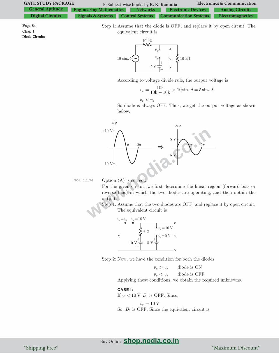
Page 84Chap 1Diode Circuits
Page 84Chap 1Diode Circuits
www.nodia.co.in
GATE STUDY PACKAGE Electronics & Communication
Buy Online: shop.nodia.co.in *Shipping Free* *Maximum Discount*
10 Subject-wise books by R. K. KanodiaNetworks Electronic Devices Analog Circuits
Digital Circuits Signals & Systems Control Systems ElectromagneticsCommunication SystemsGeneral Aptitude Engineering Mathematics
Step 1: Assume that the diode is OFF, and replace it by open circuit. The equivalent circuit is
According to voltage divide rule, the output voltage is
vo 10 5sin sink kk t t10 10
10 w w#= + =
vp v< n
So diode is always OFF. Thus, we get the output voltage as shown below.
SOL 1.1.34 Option (A) is correct.For the given circuit, we first determine the linear region (forward bias or reverse bias) in which the two diodes are operating, and then obtain the output.Step 1: Assume that the two diodes are OFF, and replace it by open circuit.
The equivalent circuit is
Step 2: Now, we have the condition for both the diodes
vp v> n diode is ON
vp v< n diode is OFF Applying these conditions, we obtain the required unknowns.
CASE I: If 10 Vv <i D1 is OFF. Since,
vo 10 V= So, D2 is OFF. Since the equivalent circuit is

Page 85Chap 1
Diode Circuits
Page 85Chap 1
Diode Circuits
www.nodia.co.in
Buy Online: shop.nodia.co.in *Shipping Free* *Maximum Discount*
GATE STUDY PACKAGE Electronics & Communication
Sample Chapter of Analog Circuits (Vol-5, GATE Study Package)
The output voltage is
vo 10 V=
CASE II: If 10 Voltv >i , D1 is ON, i.e.
vo vi= So, D2 is OFF. Since the equivalent circuit is
The output voltage is
vo vi=Step 3: In both cases diode D2 is always OFF. From the results obtained in
above steps, we get the transfer characteristic as
SOL 1.1.35 Option (D) is correct.For the given input signal, we obtain the output in following steps:
Step 1: In the positive half cycle (when 4V V>in ), diode D2 conducts and D1 will be off. So, the equivalent circuit is
So, the output voltage is
Vout 4 Volt= + This is the maximum output voltage.
Step 2: In the negative half cycle diode D1 conducts and D2 will be off so the circuit is

Page 86Chap 1Diode Circuits
Page 86Chap 1Diode Circuits
www.nodia.co.in
GATE STUDY PACKAGE Electronics & Communication
Buy Online: shop.nodia.co.in *Shipping Free* *Maximum Discount*
10 Subject-wise books by R. K. KanodiaNetworks Electronic Devices Analog Circuits
Digital Circuits Signals & Systems Control Systems ElectromagneticsCommunication SystemsGeneral Aptitude Engineering Mathematics
Applying KVL,
10kI IV 4 10kin - + - 0=
20k
V 4in + I=
Since, the minimum input voltage is Vin 10 V=- , so we obtain the corresponding current as
I 20k10 4
103 mA= - + =-
Thus, the minimum output voltage is obtained as
V V10
in out- I=
10k
V10 out- - m103=-
Vout ( )10 3=- - 7=- volt
SOL 1.1.36 Option (A) is correct.This is a half-wave rectifier circuit. So, the dc voltage is given by,
Vdc Vm
p=
Equivalent circuit with forward resistance is
So, the dc current in the circuit is
Idc ( )( / )
r R
VV5 45f
mmp p=
+=
+ V
50m
p=
SOL 1.1.37 Option (B) is correct.For the given input voltage, we consider the following two cases.
CASE I:For positive half cycle 4 Vv <o^ h, the equivalent circuit is
By using voltage divider rule,

Page 87Chap 1
Diode Circuits
Page 87Chap 1
Diode Circuits
www.nodia.co.in
Buy Online: shop.nodia.co.in *Shipping Free* *Maximum Discount*
GATE STUDY PACKAGE Electronics & Communication
Sample Chapter of Analog Circuits (Vol-5, GATE Study Package)
vo 1 11 10 sink kk tw= +
vo sin t5 w=For peak positive value of input zener diode will be ON state So,
vo . .3 3 0 7= + vo 4 V=
CASE II:For negative value of input, the zener diode will be in OFF state. So, the equivalent circuit is
So, we get the output voltage as
vo 10 sink kk t1 1
1 w#=- +
5 sin tw=-Thus, we have the peak value
vo 5=-
SOL 1.1.38 Option (C) is correct.When the switch is opened, current flows through capacitor and diode is ON in this condition. So, the equivalent circuit during TOFF is
I C dtdVc=
& Vc ( )CI t V 0c= +
Initially, ( )V 0c 0=
Vc CI t=
At t Toff= , Vc CI Toff=
So, the duty cycle is
D T TT
TT
ON OFF
ON ON= + =
TON DT=

Page 88Chap 1Diode Circuits
Page 88Chap 1Diode Circuits
www.nodia.co.in
GATE STUDY PACKAGE Electronics & Communication
Buy Online: shop.nodia.co.in *Shipping Free* *Maximum Discount*
10 Subject-wise books by R. K. KanodiaNetworks Electronic Devices Analog Circuits
Digital Circuits Signals & Systems Control Systems ElectromagneticsCommunication SystemsGeneral Aptitude Engineering Mathematics
TOFF T TON= - T DT= -
So, Vc ( )CI T DT= -
( )CI D T1= -
During TOFF, output voltage is
Vo 0 volt= .
SOL 1.1.39 Option (B) is correct.When the switch is closed, diode is off and the circuit is,
In steady state condition,
C dtdVc I2=
I2 CCI= dt
dVCIca =
Vo V CI tc=- = -
Average output voltage,
Vo T CI t dt dt1 0
TDT T
00
OFFON= - +=
b l; E##
.T CI t1
2
DT2
0=- : D
. .T CI D T1
22 2
=- .CI D T2
2
=-
SOL 1.1.40 Option (C) is correct.For the given circuit, we first determine the linear region (forward bias or reverse bias) in which the three diodes are operating, and then obtain the output.Step 1: Assume that the three diodes are OFF, and replace it by open circuit.
So, equivalent circuit is
As seen by biasing of diode, for each diode the p-terminal of diode is greater than the n -terminal. So, our assumption is incorrect.
Step 2: For first iteration, assume that all three diode are ON. So, equivalent circuit is

Page 89Chap 1
Diode Circuits
Page 89Chap 1
Diode Circuits
www.nodia.co.in
Buy Online: shop.nodia.co.in *Shipping Free* *Maximum Discount*
GATE STUDY PACKAGE Electronics & Communication
Sample Chapter of Analog Circuits (Vol-5, GATE Study Package)
VC 0 0.6 0.6 V= - =- VB 0.6 0.6 0 V=- + = VA 0.6 0 0.6 0.6 VVB= - = - =- So, current I1 is
I1 10 kV10 B
W= - 1k mA1010 0= - =
Current through diode D1 is
ID1 10 kV 20A
W=- -^ h
. 1.94k mA100 6 20= - + =
Also, current I2 is
I2 10kV 10C=
- -^ h 10
. 0.94k mA0 6 10= - + =
Applying KCL at node VB ,
I1 I ID D1 2= + 1 mA 1.94 mA ID2= + ID2 0.94 0mA 1=- Applying KCL at node VC ,
I ID D2 3+ I2= 0.94 mA ID3- + 0.94 mA= ID3 1.86 0mA 2= From the result ID1 and ID3 are greater than zero and ID2 which is
less than zero, represent a contradiction. So, diode D3 will be OFF.
Step 3: For second iteration let us assume D1 and D3 are ON and D2 is OFF so
Applying KVL in Loop 1,
10 10 0.6 10kI I 20D1 1- - - - -^ h 0= In Loop 1, we have I ID1 1= . Substituting it in above expression,
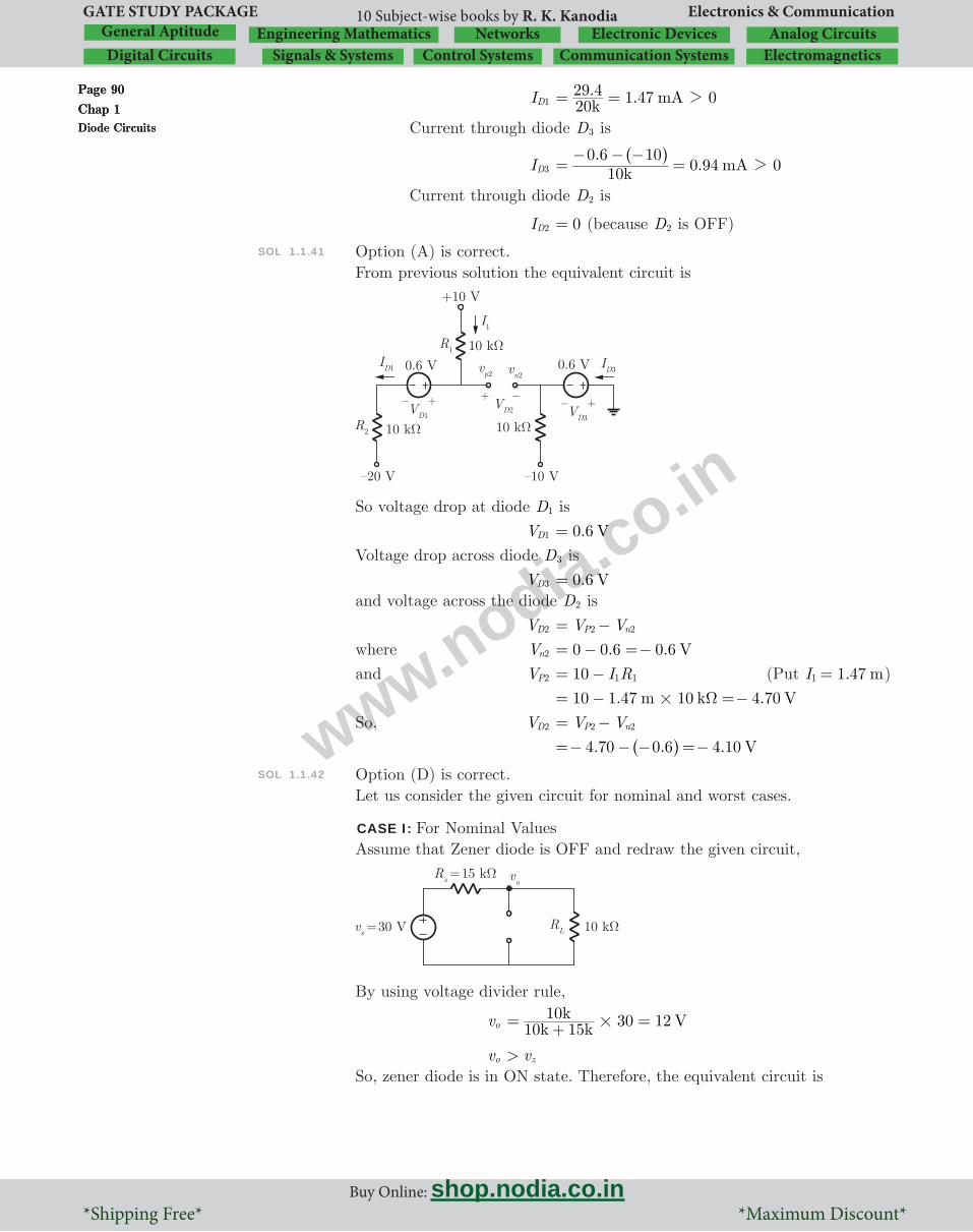
Page 90Chap 1Diode Circuits
Page 90Chap 1Diode Circuits
www.nodia.co.in
GATE STUDY PACKAGE Electronics & Communication
Buy Online: shop.nodia.co.in *Shipping Free* *Maximum Discount*
10 Subject-wise books by R. K. KanodiaNetworks Electronic Devices Analog Circuits
Digital Circuits Signals & Systems Control Systems ElectromagneticsCommunication SystemsGeneral Aptitude Engineering Mathematics
ID1 20. 1.47 0k mA29 4 2= =
Current through diode D3 is
ID3 10.
0.94 0k mA0 6 10
2=- - -
=^ h
Current through diode D2 is
ID2 0= (because D2 is OFF)
SOL 1.1.41 Option (A) is correct.From previous solution the equivalent circuit is
So voltage drop at diode D1 is
VD1 0.6 V=Voltage drop across diode D3 is
VD3 0.6 V=and voltage across the diode D2 is
VD2 V VP n2 2= -where Vn2 0 0.6 0.6 V= - =-and VP2 I R10 1 1= - (Put 1.47 mI1 = )
10 1.47 10 4.70m k VW#= - =-So, VD2 V VP n2 2= - 4.70 . 4.10 V0 6=- - - =-^ h
SOL 1.1.42 Option (D) is correct.Let us consider the given circuit for nominal and worst cases.
CASE I: For Nominal ValuesAssume that Zener diode is OFF and redraw the given circuit,
By using voltage divider rule,
vo 10 1510 30 12k k
k V#= + =
vo v> z
So, zener diode is in ON state. Therefore, the equivalent circuit is

Page 91Chap 1
Diode Circuits
Page 91Chap 1
Diode Circuits
www.nodia.co.in
Buy Online: shop.nodia.co.in *Shipping Free* *Maximum Discount*
GATE STUDY PACKAGE Electronics & Communication
Sample Chapter of Analog Circuits (Vol-5, GATE Study Package)
Applying KCL at vz node,
IS I Iz L= +
or 15 k30 9
W- 10kI v 0
zz= + -
or Iz 15 10 0.5k k mA21 9= - =
So, nominal value of zener diode current is
Iznom 0.5 mA=
CASE II: For Worst ValuesFor 5 % tolerance (worst case), we have
V maxS . .30 1 05 31 5= =^ h
V minS . .30 0 95 28 5= =^ h
R maxS 15 . 15.75k k1 05 W= =^ h
R minS 15 . 14.25 k0 95 W= =^ h
R maxL 10 . 10.5k k1 05 W= =^ h
R minL 10 . 9.5 k0 95 W= =^ h
V maxz 9 . 9.45 V1 05= =^ h
V maxz 9 . 8.55 V0 95= =^ h
Iz I IS L= -
Iz RV V
RV 0
S
S z
L
z= - - -
For I maxz I maxworstz R
V VRV
min
max min
max
min
S
S z
L
z= - -
I maxworstz 14.25
. ..
.k
31 5 8 5510 58 55= - -
1.610 0.814 0.796mA m mA= - =
For I minz I minworstz R
V VRV
max
min max
min
max
S
S z
L
z= - -
I minworstz 15.75
. .9.5.
k k28 50 9 45 9 45= - -
1.209 0.99 0.215mA mA mA= - =
SOL 1.1.43 Option (C) is correct.From the solution obtained in previous problem,
Iznom 0.50 mA=
So, Pznom V Iz
nomz
nom= ^ h
9 0.5 4.5 mW#= =In calculation of Imax
z we use V minz . So, P max
z is also calculated for the same condition. Therefore, the maximum power dissipation is
P maxz V Imin max
z z= 8.55 0.796 6.81m mW#= =Similarly, P min
z V Imax minz z=

Page 92Chap 1Diode Circuits
Page 92Chap 1Diode Circuits
www.nodia.co.in
GATE STUDY PACKAGE Electronics & Communication
Buy Online: shop.nodia.co.in *Shipping Free* *Maximum Discount*
10 Subject-wise books by R. K. KanodiaNetworks Electronic Devices Analog Circuits
Digital Circuits Signals & Systems Control Systems ElectromagneticsCommunication SystemsGeneral Aptitude Engineering Mathematics
9.45 0.215 2.03m mW#= =
SOL 1.1.44 Option (B) is correct.For the given circuit, we determine the linear region (forward bias or reverse bias) in which the two diode are operating.Step 1: Assume that the two diodes are OFF, and replace it by open circuit.
So, equivalent circuit is
Step 2: Now, we have the condition for both the diodes
vp v> n diode is ON
vp v< n diode is OFF For these condition, we conclude from the above circuit that diode
D1 is ON and diode D2 is OFF.
Step 3: For the result obtained in above step, we draw the equivalent circuit as
Thus, D1 is ON and D2 is OFF is correct option.
SOL 1.1.45 Option (D) is correct.For the given circuit, we determine the linear region (forward bias or reverse bias) in which the diode are operating.Step 1: Assume that the diodes are OFF, and replace it by open circuit. So,
equivalent circuit is

Page 93Chap 1
Diode Circuits
Page 93Chap 1
Diode Circuits
www.nodia.co.in
Buy Online: shop.nodia.co.in *Shipping Free* *Maximum Discount*
GATE STUDY PACKAGE Electronics & Communication
Sample Chapter of Analog Circuits (Vol-5, GATE Study Package)
Step 2: Now, we have the condition for both the diodes
vp v> n diode is ON
vp v< n diode is OFF Applying these conditions to above circuit, we conclude that D1, D2
, D3 are ON.
Step 3: If D1, D2, D3 are ON, then equivalent circuit is
Current I1 3 1.667k mA10 5= - =
Current I2 7 0.714k mA5 0= - =
Applying KCL at vA node,
i iD1 2+ I2= iD2 0.714 1.667mA m= - 0.9527 mA=- So, diode D2 is OFF because i 0D2 1
Step 4: For diode D2 to be OFF, the modified circuit is
Current i1 k k mA3 710 0 1= +
- =
Current i3 . k mA2 50 5
2=- -
=^ h
Applying KCL at Node VB ,
i iD1 3+ i3= iD3 2 1 1m mA mA= - = ID3 02 So, diode D3 is ON.
Step 5: Thus, from the above results, we have
D1 D2 D3
FB RB FB

Page 94Chap 1Diode Circuits
Page 94Chap 1Diode Circuits
www.nodia.co.in
GATE STUDY PACKAGE Electronics & Communication
Buy Online: shop.nodia.co.in *Shipping Free* *Maximum Discount*
10 Subject-wise books by R. K. KanodiaNetworks Electronic Devices Analog Circuits
Digital Circuits Signals & Systems Control Systems ElectromagneticsCommunication SystemsGeneral Aptitude Engineering Mathematics
SOL 1.1.46 Option (C) is correct.Since, 15 V voltage source is used for biasing the diodes. So, the applied voltage will turn both diodes ON. Therefore, we get the equivalent circuit as
In this case, the voltage across the parallel arm is not same. So it does not follow the KVL rule. When the supply is turned ON, it will increase from 0 to 15 V within milliseconds. During the rise in voltage across the diodes, when 0.3 V is established across the germanium diode it will turn ‘ON’ and maintain a level of 0.3 V. So, silicon diode always remains OFF. Therefore, we get the equivalent circuit as
SOL 1.1.47 Option (C) is correct.For the given circuit, we first determine the region (ON or OFF region) in which the zener diode is operating, and then obtain the output.Step 1: Assume that the zener diode is OFF, and replace it by open circuit.
Condition for ON state of zener diode is
VA vz$ Since, zener diode will be ON. So, we have
V minA 20 V= By using voltage divider rule,
VA R RR v
L
LL#= +
V minA R RR v min
L
Li#= +
v mini RR R
v minL
LA#=
+^ h

Page 95Chap 1
Diode Circuits
Page 95Chap 1
Diode Circuits
www.nodia.co.in
Buy Online: shop.nodia.co.in *Shipping Free* *Maximum Discount*
GATE STUDY PACKAGE Electronics & Communication
Sample Chapter of Analog Circuits (Vol-5, GATE Study Package)
12001200 220 20#= +
23.67 V= So, the load current is
iL 1.2 1.2 16.67k k mAV 0 20z= - = =
Applying KCL at node VA,
IR I Iz L= + I maxR I Imaxz L= +
Rv vmaxi z- .m mA60 16 67= +
v maxi 76.67 220m vz#= + . 36.87V V V16 87 20= + =
SOL 1.1.48 Option (D) is correct.For the given input waveform, we obtain the output voltage waveform considering the positive and negative half cycles.
CASE I:For positive half wave of the input, the diode D1 and D3 will be forward biased and diode D2, D4 will be reverse diode. So, equivalent circuit diagram is
Applying KVL in Loop 1,
v vo i+ 0= vo vi=- ...(1)
CASE II:For negative half cycle of the input, the diode D4 and D2 will be ON, and D1 and D3 will be OFF. So, the equivalent circuit is
Applying KVL in Loop 2,
v v 0o i- + 0= vo vi=Thus, from the obtained results in above two cases, we get the complete output waveform as

Page 96Chap 1Diode Circuits
Page 96Chap 1Diode Circuits
www.nodia.co.in
GATE STUDY PACKAGE Electronics & Communication
Buy Online: shop.nodia.co.in *Shipping Free* *Maximum Discount*
10 Subject-wise books by R. K. KanodiaNetworks Electronic Devices Analog Circuits
Digital Circuits Signals & Systems Control Systems ElectromagneticsCommunication SystemsGeneral Aptitude Engineering Mathematics
SOL 1.1.49 Option (B) is correct.For the given problem, we analyze the clamper circuit asStep 1: In clamper circuit, the capacitor in series and diode in shunt. In peak
detector diode is in series and capacitor in shunt. So, we conclude that circuit given in options (a), (b), and (c) are clamper circuit, but the circuit given in option (d) is peak detector.
Step 2: Again, we observe that the output waveform is clamped downward the reference voltage, it means the direction of diode must be in downward direction and the reference voltage is 2 VV = . Thus, option (b) follows the condition.
SOL 1.1.50 Option (B) is correct.
Given the circuit,
So, the current flowing through resistor R1 is given by
I RV Vad out
1= -
. 6 mA1003 2 4= - =
Since, no current is drawn by cellphone, so this current I flows through each diode and hence diode current equation is
I I eS VV
T
D
=
or 6 m 26800
mmI eS=
or IS 2.602 10 A16#= -
SOL 1.1.51 Option (B) is correct.When there is no load RL 3=^ h, I 0L = . Under this condition, maximum current flows through the zener diode. So, maximum current passing through zener is IzM , when load current is zero. This current is more than IzT , so voltage across zener diode changes due to small zener resistance. Therefore, the maximum zener voltage is
V maxz^ h V I I Rmaxz z zT z= + -^ h
76 21m m12 9= + -^ h
12 0.495 12.5 V= + =Similarly, we obtain the minimum Zener voltage as

Page 97Chap 1
Diode Circuits
Page 97Chap 1
Diode Circuits
www.nodia.co.in
Buy Online: shop.nodia.co.in *Shipping Free* *Maximum Discount*
GATE STUDY PACKAGE Electronics & Communication
Sample Chapter of Analog Circuits (Vol-5, GATE Study Package)
V minz^ h V I I Rminz zT z z= - -^ h
V I I Rz zT zK z= - -^ h
12 9 11.82m V21 1= - - =^ h
SOL 1.1.52 Option (B) is correct.Consider the given circuit,
Applying KCL at node A,
IL I IS z= - I maxL^ h I Imax minS z= -^ h
RV V I R Imini z zk z
zk= - - -
. 1m33024 11 82 1 9#= - - -
36.88 1 35.88m m mA= - =
SOL 1.1.53 Option (A) is correct.When load current is maximum, the load resistance will be
RL IV
max
min
L
z=
35.88. 329.43m
11 82 W= =
SOL 1.1.54 Option (A) is correct.For the given circuit, we first determine the region (ON or OFF region) in which the zener diode is operating, and the normal diode is forward or reverse then obtain the output.Step 1: Assume that the zener diode is OFF, and replace it by open circuit
Zener diode operates in ON state, if
Vref vz$Step 2: From the biasing, we observe that the diode is in forward bias and
zener diode is in ON state So, equivalent circuit is

Page 98Chap 1Diode Circuits
Page 98Chap 1Diode Circuits
www.nodia.co.in
GATE STUDY PACKAGE Electronics & Communication
Buy Online: shop.nodia.co.in *Shipping Free* *Maximum Discount*
10 Subject-wise books by R. K. KanodiaNetworks Electronic Devices Analog Circuits
Digital Circuits Signals & Systems Control Systems ElectromagneticsCommunication SystemsGeneral Aptitude Engineering Mathematics
The reference voltage for the circuit is
Vref V Vz= + g
6.2 0.7 6.9 V= + =Step 3: Thus, the temperature coefficient is obtained as
V VV V
z f
z z f fa a++
.. . 1.8m
6 96 2 100
0 02#
=+ -^ h
.. .m m
6 91 24 1 8= -
.. /m C6 9
0 56 c=-
. /m C0 0811 c=- . %/ C0 008 c=-
SOL 1.1.55 Option (B) is correct.The new value of Vref at 50 Cc V Tref #T= + temperature coefficient
. . m6 9 0 56 50 25#= - -^ h
6.9 0.014 6.886 V= - =
SOL 1.1.56 Option (C) is correct.For the given circuit, we determine the linear region (forward bias or reverse bias) in which the two diodes are operating.Step 1: Assume that the two diodes are OFF, and replace it by open circuit.
So, the equivalent circuit is
Step 2: Now, we have the condition for both the diodes
vp v> n diode is ON
vp v< n diode is OFF Applying these conditions, we conclude that the diodes ,D D1 2 are
ON.
Step 3: When both diodes are operating in ON state, we have the equivalent network as
By nodal analysis, we obtain the voltage at node A as
1k kV V
20 10- +
- -^ h 5m=

Page 99Chap 1
Diode Circuits
Page 99Chap 1
Diode Circuits
www.nodia.co.in
Buy Online: shop.nodia.co.in *Shipping Free* *Maximum Discount*
GATE STUDY PACKAGE Electronics & Communication
Sample Chapter of Analog Circuits (Vol-5, GATE Study Package)
2 20V V+ + m k5 2#= V3 10=-
V 310=-
Step 4: At node A voltage is negative, so we get
VPn1 0< , V 0>Pn2
Therefore, diode D1 is OFF and diode D2 is ON. So, equivalent circuit is as shown below.
From the above circuit, I 0>D2 . Thus, diode D1 is OFF and Diode D2 is ON.
SOL 1.1.57 Option (B) is correct.We have the condition for both the diodes are For normal diode,
vp v> n diode is ON
vp v< n diode is OFF For Zener diode,
| |Vpn V> z Zener diode is ON
| |Vpn V< z Zener diode is OFFUsing these conditions, we analyze the given circuit.Step 1: For positive half cycle, the diode D2, D3, D4 are operating in OFF
state and diode D1 is in forward biased for .V 0 6i 2 . Now, consider the following two cases for positive half cycle.
CASE I: If 0 10 Vvi1 1 , then zener diode is in OFF state. So, it operates
as normal diode. In this case, the voltage across zener diode V 0Pn 1. So, it operates in reverse bias.
So, output voltage v vo in=
CASE II: If 10 Vvi 2 , then voltage across zener diode is V vz2 . So, zener
diode is in ON state.

Page 100Chap 1Diode Circuits
Page 100Chap 1Diode Circuits
www.nodia.co.in
GATE STUDY PACKAGE Electronics & Communication
Buy Online: shop.nodia.co.in *Shipping Free* *Maximum Discount*
10 Subject-wise books by R. K. KanodiaNetworks Electronic Devices Analog Circuits
Digital Circuits Signals & Systems Control Systems ElectromagneticsCommunication SystemsGeneral Aptitude Engineering Mathematics
So, the output voltage is
vo 9.4 0.6 10 V= + =Step 2: For negative half cycle, the diode D1 is in reverse bias. So, no more
use of zener diode and diode D2, D3, D4 are ON if 1.8 Vv <i - other wise it is OFF. Consider the following cases for negative half cycle.
CASE I: When .1 8- v 0in1 1 , the equivalent circuit is
So, the output voltage is
vo vin=
CASE II: If vin 1.8 V1- , then diode D2, D3 and D4 is in ON state. So,
equivalent circuit is
Therefore, the output voltage is
vo . . .0 6 0 6 0 6=- - - 1.8 V=-Step 3: From the above results, we sketch the plot between vin and vo as
SOL 1.1.58 Option (B) is correct.For the given circuit, we determine the linear region (forward bias or reverse bias) in which the two diodes are operating.

Page 101Chap 1
Diode Circuits
Page 101Chap 1
Diode Circuits
www.nodia.co.in
Buy Online: shop.nodia.co.in *Shipping Free* *Maximum Discount*
GATE STUDY PACKAGE Electronics & Communication
Sample Chapter of Analog Circuits (Vol-5, GATE Study Package)
Step 1: Assume that the two diodes are OFF, and replace it by open circuit. So, the equivalent circuit is
Step 2: By using voltage divide rule, we have
vP2 k kk V5 10
5 15 5#= + =
So, voltage across diodes D1 and D2 are
vPn1 15 V= and vPn2 5 V=Step 3: Now, we have the operating conditions for the diode
vp v> n diode is ON
vp v< n diode is OFF Applying these conditions, we conclude that both diodes are
operating in ON state. But, the n -terminals of diode are commonly connected, so the result is incorrect.
Step 4: For the obtained voltage, we conclude that diode D1 approaches the ON state first. So, we check for D1 ON and D2 OFF. The equivalent circuit is
Step 5: By using voltage divider rule, we have
vP2 5k kk V5 10
5 15#= + =
vn2 15 10k kk V5 10
10#= + =
So, voltage across diode D2 is
vPn2 5 10= - vPn2 5=- vPn2 01 i.e. diode D2 is OFF (assumption is correct). Thus, diode D1 is ON
and D2 is OFF.
SOL 1.1.59 Option (C) is correct.For the given circuit, we determine the linear region (forward bias or reverse bias) in which the diodes are operating.Step 1: Assume that all the diodes are OFF, and replace it by open circuit.

Page 102Chap 1Diode Circuits
Page 102Chap 1Diode Circuits
www.nodia.co.in
GATE STUDY PACKAGE Electronics & Communication
Buy Online: shop.nodia.co.in *Shipping Free* *Maximum Discount*
10 Subject-wise books by R. K. KanodiaNetworks Electronic Devices Analog Circuits
Digital Circuits Signals & Systems Control Systems ElectromagneticsCommunication SystemsGeneral Aptitude Engineering Mathematics
So, the equivalent circuit is
Step 2: By using voltage divider rule,
V1 k k k kk
1 1 1 11 15 15#= + + + - -^^ hh
V1 30 7.5 V41#= =
Voltage across diode D1 is
vPn1 v vP n1 1= - 0 7.5 VV1= - = vPn1 02Step 3: Now, we have the condition for the diode
vp v> n diode is ON
vp v< n diode is OFF For these conditions, we conclude that diode D1 is ON.
Step 4: Now, we draw the equivalent circuit (for the diode D1 ON) for checking the operating regions of diodes D2 and D3.
Step 5: Using voltage divider rule,
V2 k k kk V1 1 1
1 15= + + -^ h
5 V=- vPn2 v vP n2 2= - 0 5 5= - - =^ h
So, diode D2 is also ON.
Step 6: Again, we redraw the equivalent circuit (for the diodes D1 and D3 ON) for checking the operating region of diode D3.
By using voltage divider rule,
V3 .k kk V1 1
1 15 7 5W= + - =-^ h
vPn3 V VP n3 3= -

Page 103Chap 1
Diode Circuits
Page 103Chap 1
Diode Circuits
www.nodia.co.in
Buy Online: shop.nodia.co.in *Shipping Free* *Maximum Discount*
GATE STUDY PACKAGE Electronics & Communication
Sample Chapter of Analog Circuits (Vol-5, GATE Study Package)
7.5 0 7.5 V=- - =- vPn3 01 So, diode D3 is OFF.
Step 7: Thus, combining the all results obtained in above cases, we conclude that diode D1 is ON, D2 is ON, and diode D3 is OFF.
SOL 1.1.60 Option (C) is correct.From the results obtained in previous problem, we have the equivalent circuit as
Thus, we get the voltage,
V V V2 3= - . V0 7 5= - -^ h
7.5 V=and the current,
I 1 kV V1 2
W= -
10 0 0k Amp= - =
**********

Page 104Chap 1Diode Circuits
Page 104Chap 1Diode Circuits
www.nodia.co.in
GATE STUDY PACKAGE Electronics & Communication
Buy Online: shop.nodia.co.in *Shipping Free* *Maximum Discount*
10 Subject-wise books by R. K. KanodiaNetworks Electronic Devices Analog Circuits
Digital Circuits Signals & Systems Control Systems ElectromagneticsCommunication SystemsGeneral Aptitude Engineering Mathematics
SOLUTIONS 1.2
SOL 1.2.1 Correct answer is 4.For the given circuit, we first determine the linear region (forward bias or reverse bias) in which the diodes are operating, and then obtain the required unknowns.Step 1: Assume that the diodes are OFF, and replace it by open circuit. So,
equivalent circuit is,
Step 2: Now, we have the condition
vp v> n diode is ON
vp v< n diode is OFF Applying these conditions, we conclude that diode D1 is OFF and
D2 is ON.
Step 3: For the result obtained in the above case, the equivalent circuit is
i1 0 mA= , 4 mAi 5005 3
2 = - =
SOL 1.2.2 Correct answer is 3.57- .For the given circuit, we first determine the linear region (forward bias or reverse bias) in which the diodes are operating, and then obtain the output.Step 1: Assume that the diodes are OFF, and replace it by open circuit. So,
equivalent circuit is
Step 2: Now, we have the condition
vp v> n diode is ON
vp v< n diode is OFF

Page 105Chap 1
Diode Circuits
Page 105Chap 1
Diode Circuits
www.nodia.co.in
Buy Online: shop.nodia.co.in *Shipping Free* *Maximum Discount*
GATE STUDY PACKAGE Electronics & Communication
Sample Chapter of Analog Circuits (Vol-5, GATE Study Package)
Applying these conditions, we conclude that both diodes are ON. But, the p-terminals of the diodes are commonly connected, so it violates the result.
Step 3: When diode D1 is OFF, and diode D2 is ON, then equivalent circuit is
I 15.
1.287k mA10 0 7 10
=- - -
=^ h
V 10 . 10 2.87m k V1 287 #= - =-^ h
So, diode D1 is OFF (our assumption is correct).
Step 4: For the diode D1 OFF, we have
iD1 0 mA=So, vo 10 5 .k m1 287=- + ^ ^h h
3.57 V=-
SOL 1.2.3 Correct answer is 2- .For the given circuit, we first determine the linear region (forward bias or reverse bias) in which the diode is operating, and then obtain the output.Step 1: Assume that the diode is OFF, and replace it by open circuit. So,
equivalent circuit is
Step 2: By using voltage divider rule,
vA 10 1010 4 2k k
k V#= + =
vB 10 1010 8 4k k
k V#= + =
Step 3: Now, we have the condition
vp v> n diode is ON
vp v< n diode is OFF Applying these conditions, we conclude that diode is OFF.
Step 4: So, the voltage across diode is
vD 2 4 2 Vv vA B= - = - =-
SOL 1.2.4 Correct answer is 2.93.Each diode having a forward bias current or 0i >D . So, each diode is operating in ON state. Therefore, the equivalent circuit is

Page 106Chap 1Diode Circuits
Page 106Chap 1Diode Circuits
www.nodia.co.in
GATE STUDY PACKAGE Electronics & Communication
Buy Online: shop.nodia.co.in *Shipping Free* *Maximum Discount*
10 Subject-wise books by R. K. KanodiaNetworks Electronic Devices Analog Circuits
Digital Circuits Signals & Systems Control Systems ElectromagneticsCommunication SystemsGeneral Aptitude Engineering Mathematics
From the circuit,we obtain the resistance
R1 .. .
0 59 4 4 4= -
k10 W =
R2 . .
14 4 0 6
=- -^ h
k5 W =
R3 ..1 5
0 6 5=
- - -^ h
. k2 93 W =
SOL 1.2.5 Correct answer is 7.6 .If D3 is ON, then
vo . .5 0 6 4 4= - =In this case,
iD1 0< , i 0>D2
So, diode D1 is OFF and diode D2 is ON. Therefore, the equivalent circuit is
Thus, the current through the diode D2 is
iD2 .. .
k0 54 4 0 6= -
. mA7 6=
SOL 1.2.6 Correct answer is 1.07 .For the given circuit, we first determine the linear region (forward bias or reverse bias) in which the diodes are operating, and then obtain the output.Step 1: Assume that the diodes are OFF, and replace it by open circuit. So,
equivalent circuit is

Page 107Chap 1
Diode Circuits
Page 107Chap 1
Diode Circuits
www.nodia.co.in
Buy Online: shop.nodia.co.in *Shipping Free* *Maximum Discount*
GATE STUDY PACKAGE Electronics & Communication
Sample Chapter of Analog Circuits (Vol-5, GATE Study Package)
Step 2: Now, we have the condition
vp v> n diode is ON
vp v< n diode is OFF Applying these conditions, we conclude that diode D1 is OFF and D2
is ON.
Step 3: So, the equivalent circuit is
Using Nodal analysis, we obtain the output voltage as
. 0.5.k
v v9 5
10 0 6 0o o- +- -^ h
0=
v0 1.07 V=
SOL 1.2.7 Correct answer is 5.82 .If 10 Vv1 = , 5 Vv2 = , then D2 is OFF and D2 is ON. In that case, the equivalent circuit is
Using nodal analysis at node vo ,
. ..v v
9 510
0 50 6 5o o- + - - 0=
v0 5.82 V=
SOL 1.2.8 Correct answer is 0.842.For the given circuit, we first determine the linear region (forward bias or reverse bias) in which the diodes are operating, and then obtain the output.Step 1: Assume that the diodes are OFF, and replace it by open circuit. So,
the equivalent circuit is (for v1 v 02= = )

Page 108Chap 1Diode Circuits
Page 108Chap 1Diode Circuits
www.nodia.co.in
GATE STUDY PACKAGE Electronics & Communication
Buy Online: shop.nodia.co.in *Shipping Free* *Maximum Discount*
10 Subject-wise books by R. K. KanodiaNetworks Electronic Devices Analog Circuits
Digital Circuits Signals & Systems Control Systems ElectromagneticsCommunication SystemsGeneral Aptitude Engineering Mathematics
Step 2: Now, we have the condition
vp v> n diode is ON
vp v< n diode is OFF Applying these conditions, we conclude that both diodes will be ON.
Step 3: For the both diodes operating in ON condition, we have the equivalent circuit as
By using nodal analysis at node vo ,
9.5 0.5.
0.5.
k k kv v v10 0 6 0 0 6 0o o o- +
- -+
- -^ ^h h 0=
vo 0.842 V=
SOL 1.2.9 Correct answer is 8.93 .For the given circuit, we first determine the linear region (forward bias or reverse bias) in which the diodes are operating, and then obtain the output.Step 1: Assume that the diodes are OFF, and replace it by open circuit. So,
the equivalent circuit is
Step 2: Now, we have the condition
vp v> n diode is ON
vp v< n diode is OFF Applying these conditions, we conclude that diode D2 is OFF and D1
is ON.
Step 3: For the obtained operating state, the equivalent circuit is

Page 109Chap 1
Diode Circuits
Page 109Chap 1
Diode Circuits
www.nodia.co.in
Buy Online: shop.nodia.co.in *Shipping Free* *Maximum Discount*
GATE STUDY PACKAGE Electronics & Communication
Sample Chapter of Analog Circuits (Vol-5, GATE Study Package)
Using Nodal analysis, we get the output voltage as
9.5.
kv v0
5000 6 10o o- +
+ -^ h 0=
vo 8.93 V=
SOL 1.2.10 Correct answer is 8.93.In previous problem, we have obtained the output voltage
vo 8.93 V=This is the voltage at n -terminal of D2. So, the required voltage v2 to turn ON the diode D2 is
v2 . . .8 93 0 60 9 53= + = VSince, for the given problem we have 5v2 = V. So, the output in this case is same as in previous.
SOL 1.2.11 Correct answer is 9.16.Now, we have
v2 V10=which is greater than the required voltage to turn ON the diode D2. So, the diodes D1 and D2 both are ON for the given voltage. Therefore, the equivalent circuit is
Applying KCL at node vo ,
9.5 .5.
.5.
k k kv v v0 0 6 10 0 6 10o o o- +
+ -+
+ -^ ^h h 0=
or vo 9.16 V=
SOL 1.2.12 Correct answer is 0.01.Since the diodes are connected in parallel, so each diode has the current
iD .100 1= A 0.01= A
SOL 1.2.13 Correct answer is 1.4.The given circuit is

Page 110Chap 1Diode Circuits
Page 110Chap 1Diode Circuits
www.nodia.co.in
GATE STUDY PACKAGE Electronics & Communication
Buy Online: shop.nodia.co.in *Shipping Free* *Maximum Discount*
10 Subject-wise books by R. K. KanodiaNetworks Electronic Devices Analog Circuits
Digital Circuits Signals & Systems Control Systems ElectromagneticsCommunication SystemsGeneral Aptitude Engineering Mathematics
For Zener diode,
vo v> z Zener diode is ON
, vo v< z Zener diode is OFFZener diode in ON state.So, the equivalent circuit is,
According to KCL
iR i iz L= +For i ( )maxL 0i ( )minz& = iR i ( )maxL=
i ( )maxL 1.4k mA1530 9
W= - =
SOL 1.2.14 Correct answer is 0.5.We have the given circuit,
Step 1: From the circuit, the voltage across Zener diode is obtained as
V 50 16.66 V22575
#= =
Step 2: For Zener diode, we have the condition
V v> z Zener diode is ON
V v< z Zener diode is OFF Checking this condition for the obtained value V , we conclude that
V V> z
16.66 15 V> i.e. the Zener diode is ON.
Step 3: For the Zener diode operating in ON condition, the equivalent circuit is
Step 4: From the equivalent circuit, we obtain the current through Zener diode as
iR i iz L= +
iz i i 15050 15
7515
R L= - = - -
iz 33.33 mA=
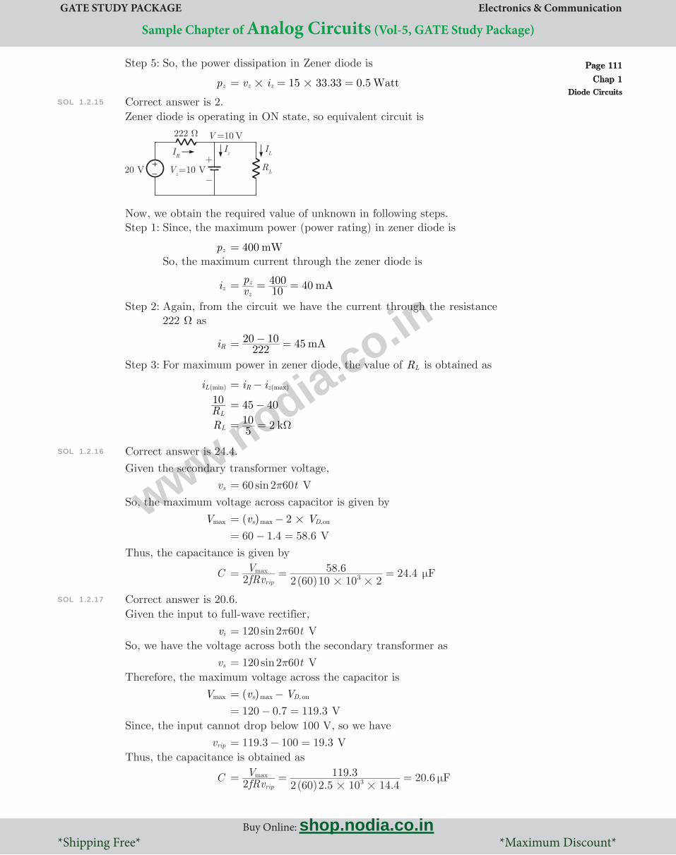
Page 111Chap 1
Diode Circuits
Page 111Chap 1
Diode Circuits
www.nodia.co.in
Buy Online: shop.nodia.co.in *Shipping Free* *Maximum Discount*
GATE STUDY PACKAGE Electronics & Communication
Sample Chapter of Analog Circuits (Vol-5, GATE Study Package)
Step 5: So, the power dissipation in Zener diode is
pz 15 33.33 0.5 Wattv iz z# #= = =
SOL 1.2.15 Correct answer is 2.Zener diode is operating in ON state, so equivalent circuit is
Now, we obtain the required value of unknown in following steps.Step 1: Since, the maximum power (power rating) in zener diode is
pz 400 mW= So, the maximum current through the zener diode is
iz 0 mAvp
10400 4
z
z= = =
Step 2: Again, from the circuit we have the current through the resistance 222 W as
iR 45 mA22220 10= - =
Step 3: For maximum power in zener diode, the value of RL is obtained as
i ( )minL i i ( )maxR z= -
R10
L 45 40= -
RL 2 k510 W= =
SOL 1.2.16 Correct answer is 24.4.
Given the secondary transformer voltage,
vs 60 2 60sin tp= V
So, the maximum voltage across capacitor is given by
Vmax ( )v V2 ,max ons D#= - 60 1.4 58.6= - = V
Thus, the capacitance is given by
C ( )
. 24.4fRvV
2 2 60 10 10 258 6max
rip3
# #= = = Fm
SOL 1.2.17 Correct answer is 20.6.Given the input to full-wave rectifier,
vi sin t120 2 60p = VSo, we have the voltage across both the secondary transformer as
vs sin t120 2 60p = VTherefore, the maximum voltage across the capacitor is
Vmax ( )v V ,max ons D= - 120 0.7 119.3= - = VSince, the input cannot drop below 100 V, so we have
vrip 119.3 100 19.3= - = VThus, the capacitance is obtained as
C ( ) . .
. 20.6 FfRvV
2 2 60 2 5 10 14 4119 3max
rip3
# #m= = =

Page 112Chap 1Diode Circuits
Page 112Chap 1Diode Circuits
www.nodia.co.in
GATE STUDY PACKAGE Electronics & Communication
Buy Online: shop.nodia.co.in *Shipping Free* *Maximum Discount*
10 Subject-wise books by R. K. KanodiaNetworks Electronic Devices Analog Circuits
Digital Circuits Signals & Systems Control Systems ElectromagneticsCommunication SystemsGeneral Aptitude Engineering Mathematics
SOL 1.2.18 Correct answer is 6.25.
Since, we know
vrip fR Cvmax
L=
So, RL 6.25fCvv
60 50 10 475max
rip5
# # #= = =- kW
SOL 1.2.19 Correct answer is 5.For the given circuit, we first determine the linear region (forward bias or reverse bias) in which the diode is operating, and then obtain the output.Step 1: Assume that the diode is OFF, and replace it by open circuit. So,
equivalent circuit is
Step 2: Now, we have the condition
vp v> n diode is ON
vp v< n diode is OFF Checking the given circuit for these conditions, we conclude that D2
is always OFF and D1 is ON.
Step 3: So, we draw the equivalent circuit for the obtained result as
Step 4: By to voltage divider rule, we obtain
vo 10 1010 10k k
k#= +
5 V=
SOL 1.2.20 Correct answer is 0.For the given circuit, we first determine the linear region (forward bias or reverse bias) in which the diodes are operating, and then obtain the output.Step 1: Assume that the diodes are OFF, and replace it by open circuit. So,
equivalent circuit is

Page 113Chap 1
Diode Circuits
Page 113Chap 1
Diode Circuits
www.nodia.co.in
Buy Online: shop.nodia.co.in *Shipping Free* *Maximum Discount*
GATE STUDY PACKAGE Electronics & Communication
Sample Chapter of Analog Circuits (Vol-5, GATE Study Package)
Step 2: Now, we have the condition
vp v> n diode is ON
vp v< n diode is OFF Checking the given circuit for the conditions,
Diode veD v 2pn1 " = =+ . So D1 is ON.
Diode veD v 2pn2 " =- =- . So D2 is OFF.
Step 3: Thus, for the obtained result, we draw the equivalent circuit as
Step 4: From the equivalent circuit, we get
I 0=
SOL 1.2.21 Correct answer is 2.We analyze the given circuit in following steps.Step 1: Assume that Zener diode is OFF, and draw the equivalent circuit as
Step 2: For Zener diode, the operating regions are defined as
V V> z Zener diode is ON
, V V< z Zener diode is OFF Checking the given circuit for the conditions, we have
V v> z
i.e. zener diode is ON and work as a voltage regulation.
Step 3: For the obtained result, we draw the equivalent circuit as
Step 4: From the circuit, we obtain
Iz 0.1. . 2k mA3 5 3 3= - =
SOL 1.2.22 Correct answer is 0.For the given circuit, we first determine the linear region (forward bias or reverse bias) in which the two diodes are operating, and then obtain the output.

Page 114Chap 1Diode Circuits
Page 114Chap 1Diode Circuits
www.nodia.co.in
GATE STUDY PACKAGE Electronics & Communication
Buy Online: shop.nodia.co.in *Shipping Free* *Maximum Discount*
10 Subject-wise books by R. K. KanodiaNetworks Electronic Devices Analog Circuits
Digital Circuits Signals & Systems Control Systems ElectromagneticsCommunication SystemsGeneral Aptitude Engineering Mathematics
Step 1: Assume that the two diodes are OFF, and replace its by open circuit. So, the equivalent circuit is
Step 2: Now, we have the condition for both the diodes
vp v> n diode is ON
vp v< n diode is OFF Checking the given circuit for the conditions, we conclude that Vpn
of diode D2 is highly positive respect to D1. So, D1 is OFF and D2 is ON.
Step 3: For the obtained result, we draw the equivalent circuit as
From the circuit, we have
Current, I 2 6.5k mA5 8
=- -
=^ h
Voltage, V 5 6.5 1 1.5 V#= - =- So, diode D1 is OFF (assumption is correct). Therefore,
ID 0=
SOL 1.2.23 Correct answer is 1.66.We have the regulator circuit as
For R minL the load current will be maximum. Since, by applying KCL at Node A, we have
IS I IL z= +So, for I maxL the value of Iz has to be minimum, i.e.
I minz 0 mA=
or RV VS z- I0 maxL= +
or RV
minL
z 5k20 5= - Put I R
V,max
minL
L
z=: D
Thus, R minL 1.66m k35 W= =

Page 115Chap 1
Diode Circuits
Page 115Chap 1
Diode Circuits
www.nodia.co.in
Buy Online: shop.nodia.co.in *Shipping Free* *Maximum Discount*
GATE STUDY PACKAGE Electronics & Communication
Sample Chapter of Analog Circuits (Vol-5, GATE Study Package)
SOL 1.2.24 Correct answer is 3.33.Assume that zener diode is OFF and draw the equivalent circuit
By using voltage divider rule,
vo 5 11
k kk 20#= +
3.33 VAcross the zener diode the voltage is 3.33 Vvo = , and the Zener voltage is
Vv 5z = . So, we have
vo v< z
i.e. zener diode operates in OFF state (assumption is correct).Thus,
vo 3.33 V=
SOL 1.2.25 Correct answer is 12.6.For RL 3= , the equivalent circuit is
Now, we analyse the circuit in following steps.Step 1: Assume zener diode in OFF state and draw the equivalent circuit.
Step 2: From the circuit, we have
vo V30= Since Vv 9z = , so we conclude that
vo vz2 i.e. Zener diode is operating in ON state (assumption is incorrect).
Step 3: For the obtained result, we draw the equivalent circuit as
Step 4: So, the current flowing through zener diode is
Iz 15 1.4k mA30 9= - =
Step 5: Thus, the power dissipation in Zener diode is

Page 116Chap 1Diode Circuits
Page 116Chap 1Diode Circuits
www.nodia.co.in
GATE STUDY PACKAGE Electronics & Communication
Buy Online: shop.nodia.co.in *Shipping Free* *Maximum Discount*
10 Subject-wise books by R. K. KanodiaNetworks Electronic Devices Analog Circuits
Digital Circuits Signals & Systems Control Systems ElectromagneticsCommunication SystemsGeneral Aptitude Engineering Mathematics
Pz v Iz z= 9 1.4 12.6m mW#= =
SOL 1.2.26 Correct answer is 16.82.For the diode operating in ON state, simplified circuit is
The ideal dc output voltage in the absence of the ripple is given by
Vdc output^ h V Vdc input on= -^ h
Since, Vdc input^ h V 2rms input#= ^ h
12.6 17.82 V2#= =So, Vdc output^ h 17.82 1 16.82 V= - =
SOL 1.2.27 Correct answer is 0.747.Again, for the diode operating in ON state, we have the simplified circuit as
From the circuit, the ripple voltage is
Vrip RV V
CTm o. -
I CT
dc= I RV V
dcm oa = -
; E
Given that 60 Hzf = . So,
T secf1
601= =
Therefore, Vrip . /
1516 8
25 101 60
3#
#= -
0.747 V=
SOL 1.2.28 Correct answer is 0.For the given circuit, we first determine the linear region (forward bias or reverse bias) in which the diodes are operating, and then obtain the output.Step 1: Assume that the diodes are OFF, and replace it by open circuit. So,
equivalent circuit is

Page 117Chap 1
Diode Circuits
Page 117Chap 1
Diode Circuits
www.nodia.co.in
Buy Online: shop.nodia.co.in *Shipping Free* *Maximum Discount*
GATE STUDY PACKAGE Electronics & Communication
Sample Chapter of Analog Circuits (Vol-5, GATE Study Package)
Step 2: Now, we have the condition
vp v> n diode is ON
vp v< n diode is OFF Checking the given circuit for these conditions, we conclude that the
diodes D1 and D2 will be ON.
Step 3: For the obtained result, we get the equivalent circuit as
From the circuit, we obtain
ID2 5 10 1.66k k mA15 10
= +- -
=^ h
Vn2 10 1.66k m 10#= - 6.6 V=Step 4: Since, we have assumed diode D1 ON, so
Vp2 0 V= Therefore, the voltage across diode D2 is
Vpn2 01 i.e. D2 will be OFF due to D1 ON (assumption is incorrect).
Step 5: Therefore, the total current from 15 V supply will go through diode D1 and no current flow through diode D2, i.e.
ID2 0=Step 6: Thus, the actual equivalent circuit is
Current through diodes D1 and D2 are
ID1 5 3k mA15 0W= - =
ID2 0=
SOL 1.2.29 Correct answer is 1.55.For the given circuit, we first determine the linear region (forward bias or reverse bias) in which the diodes are operating, and then obtain the output.

Page 118Chap 1Diode Circuits
Page 118Chap 1Diode Circuits
www.nodia.co.in
GATE STUDY PACKAGE Electronics & Communication
Buy Online: shop.nodia.co.in *Shipping Free* *Maximum Discount*
10 Subject-wise books by R. K. KanodiaNetworks Electronic Devices Analog Circuits
Digital Circuits Signals & Systems Control Systems ElectromagneticsCommunication SystemsGeneral Aptitude Engineering Mathematics
Step 1: Assume that the diodes are OFF, and replace it by open circuit. So, equivalent circuit is
Step 2: For the equivalent circuit, we may conclude that the applied voltage forward biases the diodes. So, both the diodes are operating in ON state. So equivalent Circuit is
Step 3: For the equivalent circuit, we obtain
I2 6.6. 0.11k mA0 7
W= =
I3 RV 0B
2= -
11.2. 1.66k mA18 6 0= - =
Step 4: Again, applying KCL at node VB ,
I3 I ID2 2= + 1.66 m 0.11 mAID2= + ID2 1.55 mA=
SOL 1.2.30 Correct answer is 38.4.The diode current equation is
ID I eVV
ST
D= ...(1)
Differentiating with respect to VD ,
dVdI
D
D I eVV
V1
ST
D
T= ...(2)
So we may write
VI
D
D
TT V
IT
D=
Thus, IDT VI V
T
DD#T=
261 1 38.4mm m Am#= =
ALTERNATIVE METHOD :
We have
DC bias current, ID 1 mA=

Page 119Chap 1
Diode Circuits
Page 119Chap 1
Diode Circuits
www.nodia.co.in
Buy Online: shop.nodia.co.in *Shipping Free* *Maximum Discount*
GATE STUDY PACKAGE Electronics & Communication
Sample Chapter of Analog Circuits (Vol-5, GATE Study Package)
Small signal resistance, rd IV
D
T= 26mm
126 W= =
By ac analysis, we get small change in current as
IDT rVd
DT= 1 38.4m A26 m= =
SOL 1.2.31 Correct answer is 1.417.
The ripple voltage is given by
Vrip RV V
CT,
L
m D on= - where Vm = peak voltage
or Vrip I CT
dc=
Given that peak to peak swing is
Vpeak peak- 9 V=So, the peak voltage is obtained as
Vm . VV
2 29 4 5peak peak= = =-
Also, we have V ,D on 0.8 V= RL 0.436 W=
T 16.67 msf1
601= = =
Thus, the capacitance is obtained as
C 0.436. .
.16.67 ms4 5 0 8
0 1#W= - 1.417 F=
SOL 1.2.32 Correct answer is 0.389.Full wave rectifier with smoothing capacitor and load resistance RL is
Ripple in full wave rectifier is
The output remains equal to zero for
Vin V2 ,D on1So output voltage is
Vout V V2 ,P D on= -The capacitor is discharged for half of the input cycle (approx.), so the ripple is approximately equal to half of that in half wave rectifier. Therefore, ripple voltage in full wave rectifier is
Vrip R CV V
T21 2 ,m D on
1 1= -
.21
30 1000 10 603 2 0 8
6# # #
#= --
0.389 V=

Page 120Chap 1Diode Circuits
Page 120Chap 1Diode Circuits
www.nodia.co.in
GATE STUDY PACKAGE Electronics & Communication
Buy Online: shop.nodia.co.in *Shipping Free* *Maximum Discount*
10 Subject-wise books by R. K. KanodiaNetworks Electronic Devices Analog Circuits
Digital Circuits Signals & Systems Control Systems ElectromagneticsCommunication SystemsGeneral Aptitude Engineering Mathematics
SOL 1.2.33 Correct answer is 4.98.Load current waveform for full wave rectifier is
By definition, average or dc current is given by
Idc T i t d t1L
T
0w= ^ ^h h#
i d t21
L0
2
p w=p
^ h#The load current is given by
iL sin
sin
I t t
I t t
0
2m
m
# #
# #
w w pw p w p
=-)
So, the average dc current is obtained as
Idc sin sinI t d t I t d t21
m m0
2
p w w w w= + -p
p
p^ ^h h< F# #
cos cosI t t2m
02
p w w= - +ppp
^ ^h h8 B
I2 m
p = ...(1)
Now, the rectifier circuit is
From the circuit, we have
Im R R RV
S f L
m= + + ...(2)
Where RS " Secondary winding resistance
Rf " Diode forward resistance
RL " Load resistanceSubstituting equation (2) in equation (1), we get
Idc I
R R RV2 2m
S f L
m
p p= =
+ +^ h
Again, for positive half cycle diode D1 is ON and D2 is OFF, and for negative half cycle diode D1 is OFF and D2 is ON. Average or dc voltage Vdc is load voltage produced by Idc flowing through the load, i.e.
Vdc I R I R2dc L
m L
p= =
Substituting equation (2) in above expression, we have
Vdc R R RV R2
S f L
m L
p=
+ +^ h
Since R RS f+ R<< L , so
Vdc V2 m
p =

Page 121Chap 1
Diode Circuits
Page 121Chap 1
Diode Circuits
www.nodia.co.in
Buy Online: shop.nodia.co.in *Shipping Free* *Maximum Discount*
GATE STUDY PACKAGE Electronics & Communication
Sample Chapter of Analog Circuits (Vol-5, GATE Study Package)
Therefor, dc power delivered to the load is given by
Pdc V I I Rdc dc dc L2= =
I RR R R
V R2 2mL
S f L
mL
2 2
p p= =
+ +b^
lh; E ...(3)
Given that, VS rms^ h 20 V= RS 5 W= , 2Rf W= , 50RL W=
Vm V2 S rms= ^ h
20 28.28 V2 #= =Substituting these values in equation (3), we get
Pdc ..
3 14 5 2 502 28 28 50
2# #=+ +^ h; E
4.98 watt=
SOL 1.2.34 Correct answer is 14.In previous solution, we have obtained
Vdc R R RV R2
S f L
m L
p=
+ +^ h
For calculation of Null load voltage VNL^ h, we put RL " 3 in above expression, i.e.
VNL lim
RR RV
1
2R
L
S f
m
L p =
+ +"3d n
18.01 VV2 m
p= =
Also, the full load voltage is obtained as
VFL I RR R R
V R2dc L
S f L
m L
p= =
+ +^ h
.
.3 14 5 2 502 28 28 50# #=
+ +^ h
15.80 V=Thus, the percentage load regulation is
% Load regulation %VV V 100
FL
NL FL #= -
.. . %15 80
18 01 15 80 100 14#= - =
SOL 1.2.35 Correct answer is 0.711.The rectifier efficiency is defined as
h Input ac powerOutput dc power=
Now, we have the output dc power,
Pdc o^ h V I I Rdc dc dc L2= =
I R2 mL
2
p= b l
The input ac power is
Pac in^ h V I V V2 2
rms i rms im
i
m
i
= =^ ^ c ch h m m
V I
2m i m i=
^ ^h h
R R R
I2 S f L
m2
=+ +^ h
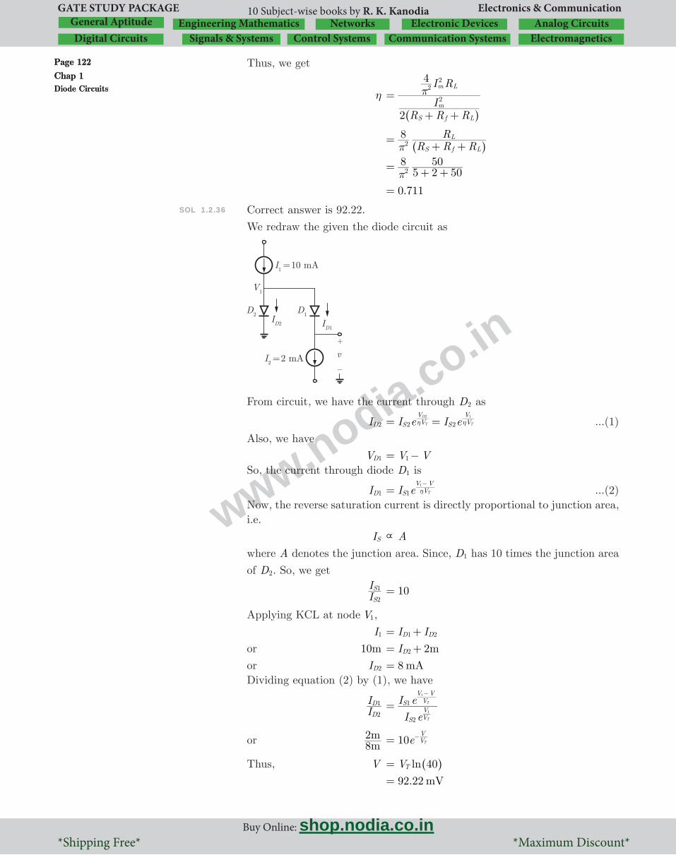
Page 122Chap 1Diode Circuits
Page 122Chap 1Diode Circuits
www.nodia.co.in
GATE STUDY PACKAGE Electronics & Communication
Buy Online: shop.nodia.co.in *Shipping Free* *Maximum Discount*
10 Subject-wise books by R. K. KanodiaNetworks Electronic Devices Analog Circuits
Digital Circuits Signals & Systems Control Systems ElectromagneticsCommunication SystemsGeneral Aptitude Engineering Mathematics
Thus, we get
h
R R RI
I R
2
4
S f L
m
m L
2
22
p=
+ +^ h
R R R
R8S f L
L2p
=+ +^ h
85 2 50
502p
= + +
.0 711=
SOL 1.2.36 Correct answer is 92.22.
We redraw the given the diode circuit as
From circuit, we have the current through D2 as
ID2 I e I eS VV
S VV
2 2T
D
T
2 1
= =h h ...(1)
Also, we have
VD1 V V1= -So, the current through diode D1 is
ID1 I eS VV V
11
T= h-
...(2)Now, the reverse saturation current is directly proportional to junction area, i.e.
IS A\
where A denotes the junction area. Since, D1 has 10 times the junction area
of D2. So, we get
IIS
S
2
1 10=
Applying KCL at node V1,
I1 I ID D1 2= +or 10m 2mID2= +or ID2 8 mA=Dividing equation (2) by (1), we have
IID
D
2
1 I e
I e
S VV
S VV V
2
1
T
T
1
1
=-
or mm
82 e10 V
VT= -
Thus, V lnV 40T= ^ h
. mV92 22=

Page 123Chap 1
Diode Circuits
Page 123Chap 1
Diode Circuits
www.nodia.co.in
Buy Online: shop.nodia.co.in *Shipping Free* *Maximum Discount*
GATE STUDY PACKAGE Electronics & Communication
Sample Chapter of Analog Circuits (Vol-5, GATE Study Package)
SOL 1.2.37 Correct answer is 31.8.All the diodes are forward biased due to 12 V supply voltage. So, diode D1
, D2, D3 are ON.
From the circuit, we have
Voltage, V1 . .12 0 7 11 3= - = Voltage, V2 12 0.7 0.7 10.6 V= - - = Voltage, V3 12 0.7 0.7 0.7 9.9 V= - - - =
Current, I3 1 kV 03
W= - 1. 9.9k mA9 9 0
W= - =
So, the current through diode D3 is
ID3 9.9 mAI3= =Again, we obtain
I2 1 kV 02
W= -
1. 10.6k mA10 6 0
W= - =
Applying KCL at node V2, we get current through diode D2 as
ID2 I ID2 3= + . .m m10 6 9 9= + 20.5 mA=From the circuit, we have the current
I1 1 kV 01
W= - . 11.3k mA111 3= =
Thus, applying KCL at node V1 we obtain the current through diode D1 as
ID1 I ID1 2= + . . .mA m mA11 3 20 5 31 8= + =
SOL 1.2.38 Correct answer is 0.5.For DC analysis, coupling capacitor C1 and C2 is open circuited. So, equivalent circuit is
Since, diode is forward biased, so current through the diode is
IDQ .R
V 0 6C
C= -
2. .
k1 6 0 6
W= -
0.5 mA=

Page 124Chap 1Diode Circuits
Page 124Chap 1Diode Circuits
www.nodia.co.in
GATE STUDY PACKAGE Electronics & Communication
Buy Online: shop.nodia.co.in *Shipping Free* *Maximum Discount*
10 Subject-wise books by R. K. KanodiaNetworks Electronic Devices Analog Circuits
Digital Circuits Signals & Systems Control Systems ElectromagneticsCommunication SystemsGeneral Aptitude Engineering Mathematics
SOL 1.2.39 Correct answer is 0.33.For ac analysis, we have the diode resistance
rd IVDQ
Th= 0.51 25 50m
mV W#= =
In ac analysis, capacitor is short circuit and dc voltage source acts as a short circuit. So, we get the small signal ac equivalent circuit is
The above circuit can be redrawn in simplified form as
Thus, by using voltage divider rule
v to ^ h || ||| | | |k k
k kv t
100 2 50 22 50 2
i= + ^ h
or v tv t
i
o
^
^
h
h .
.100 47 61
47 61= +
.0 33=
***********

Page 125Chap 1
Diode Circuits
Page 125Chap 1
Diode Circuits
www.nodia.co.in
Buy Online: shop.nodia.co.in *Shipping Free* *Maximum Discount*
GATE STUDY PACKAGE Electronics & Communication
Sample Chapter of Analog Circuits (Vol-5, GATE Study Package)
SOLUTIONS 1.3
SOL 1.3.1 Option (A) is correct.In capacitor filter,
Ripple factor, r fCR4 31
L
=
For large value of RL (load resistance) the ripple factor should be small. So it is suitable for large value of load resistance.
SOL 1.3.2 Option (B) is correct.In inductor filter,
Ripple factor, r L
R3 2
L
w=
^ hFor small value of load resistance RL^ h the ripple factor should be small. So inductor filter is suitable for small values of load-resistance.
SOL 1.3.3 Option (A) is correct.The rectifier circuit is to convert a.c. voltage to d.c. voltage.
SOL 1.3.4 Option (C) is correct.The ripple factor of Inductor filter is,
r L
R3 2
L
w=
^ hSOL 1.3.5 Option (D) is correct.
A bleeder resistance RB , is connected in parallel with the load resistance as shown in figure
It improves voltage regulation of the supply by acting as the preload on the supply.
SOL 1.3.6 Option (B) is correct.For half wave rectifier,
The output frequency fo fi=Where, fi = input frequency
fo 50 Hz=For full wave bridge rectifier
fo f2 i= 2 50#= 100 Hz=
SOL 1.3.7 Option (D) is correct.The full wave bridge diode rectifier,
% Voltage regulation %RR2
100L
f#=

Page 126Chap 1Diode Circuits
Page 126Chap 1Diode Circuits
www.nodia.co.in
GATE STUDY PACKAGE Electronics & Communication
Buy Online: shop.nodia.co.in *Shipping Free* *Maximum Discount*
10 Subject-wise books by R. K. KanodiaNetworks Electronic Devices Analog Circuits
Digital Circuits Signals & Systems Control Systems ElectromagneticsCommunication SystemsGeneral Aptitude Engineering Mathematics
%502 50 100# #=
%200=
SOL 1.3.8 Option (C) is correct.A voltage multiplier circuit is shown in figure
So essential component is capacitor.
SOL 1.3.9 Option (A) is correct.Let us assume diode is OFF.So the circuit is
V 0<pn , So diode is actually OFF.So the equivalent circuit is
Vo 10 V=
SOL 1.3.10 Option (B) is correct.
Zener diode can work in the breakdown region without getting damaged. So a Zener diode is always used in Reverse biased.
SOL 1.3.11 Option (D) is correct.Voltage regulation – it is defined as the % change in regulated output voltage

Page 127Chap 1
Diode Circuits
Page 127Chap 1
Diode Circuits
www.nodia.co.in
Buy Online: shop.nodia.co.in *Shipping Free* *Maximum Discount*
GATE STUDY PACKAGE Electronics & Communication
Sample Chapter of Analog Circuits (Vol-5, GATE Study Package)
for a change in load current from minimum to maximum value.
%VR %VV V 100
NL
NL FL #= -
So it should be as small as possible for ideal rectifier and filter circuit,
% Regulation %0=
SOL 1.3.12 Option (A) is correct.From Planck’s equation,
E hn=
Eg hCl=
Eg .
5490 106 626 10 3 10
10
34 8
## # #= -
-
3.62 10 J19#= -
2.26 eV=
SOL 1.3.13 Option (B) is correct.When the load resistance is infinity the value of the inductance will also tend to be infinity to over come this problem, a bleeder resistor RB , is connected in parallel with the load resistance as shown in Fig.
Therefore, a minimum current will always be present for optimum operation of the inductor.
SOL 1.3.14 Option (A) is correct.The given circuit is half wave rectifier circuit so
DC current, Idc Im
p= R R
VL F
m
p=
+^ h
V5 45
m
p=
+^ h V
50m
p=
SOL 1.3.15 Option (B) is correct.The relation between diode current voltage and temperature is given by
I I e 1/o
V VT= -h^ h
where Io = reverse saturation current
V = voltage across diode
VT = temperature equivalent voltage
qKT=
SOL 1.3.16 Option (A) is correct.The transformer utilization factor (TUF) is defined as,
TUF secac rating of the transformer ondarydc power delivered to the load=
RP
ratedac
dc=
SOL 1.3.17 Option (A) is correct.Peak inverse voltage (PIV) of an half wave rectifier is Vm .PIV of an full wave rectifier with centre tapped is V2 m .

Page 128Chap 1Diode Circuits
Page 128Chap 1Diode Circuits
www.nodia.co.in
GATE STUDY PACKAGE Electronics & Communication
Buy Online: shop.nodia.co.in *Shipping Free* *Maximum Discount*
10 Subject-wise books by R. K. KanodiaNetworks Electronic Devices Analog Circuits
Digital Circuits Signals & Systems Control Systems ElectromagneticsCommunication SystemsGeneral Aptitude Engineering Mathematics
SOL 1.3.18 Option (A) is correct.For inductor filter,
Ripple factor, r L
R3 2
L
w=
^ hSo the ripple factor value is low for low value of load resistance and low value of load resistance means for heavy load currents.
SOL 1.3.19 Option (B) is correct.The minimum value of inductance required to make the current to flow through the circuit at all times is known as critical inductance. It depends on load resistance and supply frequency. It is given by,
The critical inductance Lc R3
Lw=
SOL 1.3.20 Option (C) is correct.Transformer utilization factor,
For Half wave rectifier, TUF .0 287=For Full wave centre tapped rectifier,
TUF .0 693=For Full wave bridge rectifier,
TUF .0 812=So, TUF is more in bridge rectifier.
SOL 1.3.21 Option (A) is correct.Zener diode is in OFF state. So, it work as voltage regulator.So, equivalent circuit is,
KCL at node A
IS I IL z= +For maximum load current,
I maxS^ h I Imin minL z= +^ ^h h
RV Vmax
S
i z-^ h 0.5mI maxL= +^ h
I maxL^ h . 0.5m1000
30 5 8= - -
24. .m m2 0 5= - 23.7 mAmp=
SOL 1.3.22 Option (C) is correct.
SOL 1.3.23 Option (C) is correct.The p-section filter circuit is,
At no load, RL 3=

Page 129Chap 1
Diode Circuits
Page 129Chap 1
Diode Circuits
www.nodia.co.in
Buy Online: shop.nodia.co.in *Shipping Free* *Maximum Discount*
GATE STUDY PACKAGE Electronics & Communication
Sample Chapter of Analog Circuits (Vol-5, GATE Study Package)
So current flow through is zero.
SOL 1.3.24 Option (A) is correct.
The Diode D1 is ON due to 6 V and due to D1 is F.B. D2 is always in R.B.So equivalent circuit is,
So, V2 .6 0 6= - 5.4 V= V1 6 V=
SOL 1.3.25 Option (B) is correct.The given circuit is,
This is a clamper circuit and the diode is in downward direction the total signal will be clamp below the reference voltage.
SOL 1.3.26 Option (D) is correct.Clipper circuits, also called limiter circuits are used to eliminate portion of a signal that are above or below a specified level without distorting the remaining part of the alternating waveform.
SOL 1.3.27 Option (D) is correct.Clamper circuits shifts the entire signal voltage by a dc level.
SOL 1.3.28 Option (C) is correct.
IZM .VP
6 8500 10
Z
ZM3
#= =-
. .A mA73 5 10 73 53#= =-

Page 130Chap 1Diode Circuits
Page 130Chap 1Diode Circuits
www.nodia.co.in
GATE STUDY PACKAGE Electronics & Communication
Buy Online: shop.nodia.co.in *Shipping Free* *Maximum Discount*
10 Subject-wise books by R. K. KanodiaNetworks Electronic Devices Analog Circuits
Digital Circuits Signals & Systems Control Systems ElectromagneticsCommunication SystemsGeneral Aptitude Engineering Mathematics
SOL 1.3.29 Option (D) is correct.
rZ . 5IV
10 100 05
Z
Z3
#TT W= = =-
SOL 1.3.30 Option (A) is correct.
ZVl 4.7 15 5 VV I r 20 10Z Z Z3
# #= + = + =-^ h
SOL 1.3.31 Option (B) is correct.
SOL 1.3.32 Option (D) is correct.The output of a rectifier consists of d.c. component as well as a.c. component. The a.c. component in the output is called as ripple. So the ripple factor g^ h is the ratio of ripple voltage or effective value of a.c. component voltage to the average or d.c. voltage, so it defined the purity of output power.
g . .. .
d c value of waverms value of a c component=
SOL 1.3.33 Option (B) is correct.
SOL 1.3.34 Option (B) is correct.
SOL 1.3.35 Option (A) is correct.
SOL 1.3.36 Option (D) is correct.
Vm 20 V2=
Vdc Vm
p=
20 2p=
9 V=
***********

Eighth Edition
GATEELECTRONICS & COMMUNICATION
Communication SystemsVol 9 of 10
RK Kanodia & Ashish Murolia
NODIA & COMPANY

GATE Electronics & Communication Vol 9, 7eCommunication SystemsRK Kanodia & Ashish Murolia
Copyright © By NODIA & COMPANY
Information contained in this book has been obtained by author, from sources believes to be reliable. However, neither NODIA & COMPANY nor its author guarantee the accuracy or completeness of any information herein, and NODIA & COMPANY nor its author shall be responsible for any error, omissions, or damages arising out of use of this information. This book is published with the understanding that NODIA & COMPANY and its author are supplying information but are not attempting to render engineering or other professional services.
MRP 490.00
NODIA & COMPANYB 8, Dhanshree Ist, Central Spine, Vidyadhar Nagar, Jaipur 302039Ph : +91 141 2101150, www.nodia.co.inemail : [email protected]
Printed by Nodia and Company, Jaipur

Preface to the Series
For almost a decade, we have been receiving tremendous responses from GATE aspirants for our earlier books: GATE Multiple Choice Questions, GATE Guide, and the GATE Cloud series. Our first book, GATE Multiple Choice Questions (MCQ), was a compilation of objective questions and solutions for all subjects of GATE Electronics & Communication Engineering in one book. The idea behind the book was that Gate aspirants who had just completed or about to finish their last semester to achieve his or her B.E/B.Tech need only to practice answering questions to crack GATE. The solutions in the book were presented in such a manner that a student needs to know fundamental concepts to understand them. We assumed that students have learned enough of the fundamentals by his or her graduation. The book was a great success, but still there were a large ratio of aspirants who needed more preparatory materials beyond just problems and solutions. This large ratio mainly included average students.
Later, we perceived that many aspirants couldn’t develop a good problem solving approach in their B.E/B.Tech. Some of them lacked the fundamentals of a subject and had difficulty understanding simple solutions. Now, we have an idea to enhance our content and present two separate books for each subject: one for theory, which contains brief theory, problem solving methods, fundamental concepts, and points-to-remember. The second book is about problems, including a vast collection of problems with descriptive and step-by-step solutions that can be understood by an average student. This was the origin of GATE Guide (the theory book) and GATE Cloud (the problem bank) series: two books for each subject. GATE Guide and GATE Cloud were published in three subjects only.
Thereafter we received an immense number of emails from our readers looking for a complete study package for all subjects and a book that combines both GATE Guide and GATE Cloud. This encouraged us to present GATE Study Package (a set of 10 books: one for each subject) for GATE Electronic and Communication Engineering. Each book in this package is adequate for the purpose of qualifying GATE for an average student. Each book contains brief theory, fundamental concepts, problem solving methodology, summary of formulae, and a solved question bank. The question bank has three exercises for each chapter: 1) Theoretical MCQs, 2) Numerical MCQs, and 3) Numerical Type Questions (based on the new GATE pattern). Solutions are presented in a descriptive and step-by-step manner, which are easy to understand for all aspirants.
We believe that each book of GATE Study Package helps a student learn fundamental concepts and develop problem solving skills for a subject, which are key essentials to crack GATE. Although we have put a vigorous effort in preparing this book, some errors may have crept in. We shall appreciate and greatly acknowledge all constructive comments, criticisms, and suggestions from the users of this book. You may write to us at [email protected] and [email protected].
Acknowledgements
We would like to express our sincere thanks to all the co-authors, editors, and reviewers for their efforts in making this project successful. We would also like to thank Team NODIA for providing professional support for this project through all phases of its development. At last, we express our gratitude to God and our Family for providing moral support and motivation.
We wish you good luck ! R. K. KanodiaAshish Murolia

SYLLABUS
GATE Electronics & Communications:
Random signals and noise: probability, random variables, probability density function, autocorrelation, power spectral density. Analog communication systems: amplitude and angle modulation and demodulation systems, spectral analysis of these operations, superheterodyne receivers; elements of hardware, realizations of analog communication systems; signal-to-noise ratio (SNR) calculations for amplitude modulation (AM) and frequency modulation (FM) for low noise conditions. Fundamentals of information theory and channel capacity theorem. Digital communication systems: pulse code modulation (PCM), differential pulse code modulation (DPCM), digital modulation schemes: amplitude, phase and frequency shift keying schemes (ASK, PSK, FSK), matched filter receivers, bandwidth consideration and probability of error calculations for these schemes. Basics of TDMA, FDMA and CDMA and GSM.
GATE Instrumentation Signals, Systems and Communications: Periodic and aperiodic signals. Impulse response, transfer function and frequency response of first- and second order systems. Convolution, correlation and characteristics of linear time invariant systems. Discrete time system, impulse and frequency response. Pulse transfer function. IIR and FIR filters. Amplitude and frequency modulation and demodulation. Sampling theorem, pulse code modulation. Frequency and time division multiplexing. Amplitude shift keying, frequency shift keying and pulse shift keying for digital modulation.
IES Electronics & Telecommunication
Communication Systems: Basic information theory; Modulation and detection in analogue and digital systems; Sampling and data reconstructions; Quantization & coding; Time division and frequency division multiplexing; Equalization; Optical Communication: In free space & fiber optic; Propagation of signals at HF, VHF, UHF and microwave frequency; Satellite Communication.
IES Electrical
Communication Systems Types of modulation; AM, FM and PM. Demodulators. Noise and bandwidth considerations. Digital communication systems. Pulse code modulation and demodulation. Elements of sound and vision broadcasting. Carrier communication. Frequency division and time division multiplexing, Telemetry system in power engineering.

CONTENTS
CHAPTER 1 RANDOM VARIABLE
1.1 INTRODUCTION 1
1.2 PROBABILITY 1
1.2.1 Joint Probability 2
1.2.2 Conditional Probability 2
1.2.3 Statistical Independence 2
1.3 RANDOM VARIABLE 2
1.3.1 Discrete Random Variable 2
1.3.2 Continuous Random Variable 3
1.4 TRANSFORMATION OF RANDOM VARIABLES 4
1.5 MULTIPLE RANDOM VARIABLES 4
1.6 STATISTICAL AVERAGE OF RANDOM VARIABLE 5
1.6.1 Mean or Expected Value 5
1.6.2 Moments 6
1.6.3 Variance 6
1.6.4 Standard Deviation 6
1.6.5 Characteristic Function 6
1.6.6 Joint Moments 6
1.6.7 Covariance 6
1.6.8 Correlation Coefficient 7
1.7 SOME IMPORTANT PROBABILITY DISTRIBUTIONS 7
1.7.1 Binomial Distribution 8
1.7.2 Poisson Distribution 8
1.7.3 Gaussian Distribution 8
1.7.4 Rayleigh Distribution 10
EXERCISE 1.1 11
EXERCISE 1.2 26
EXERCISE 1.3 33
SOLUTIONS 1.1 34
SOLUTIONS 1.2 61
SOLUTIONS 1.3 81
CHAPTER 2 RANDOM PROCESS
2.1 INTRODUCTION 82
2.2 RANDOM PROCESS 82
2.2.1 Classification of Random Process 83
2.2.2 Probability Density Function of Random Process 83
2.2.3 Stationary Random Process 83
2.3 AVERAGES OF RANDOM PROCESS 84
2.3.1 Time Average of a Random Process 84

2.3.2 Ensemble Average of a Random Process 84
2.3.3 Autocorrelation function 84
2.3.4 Cross-Correlation Function 85
2.3.5 Autocovariance Function 85
2.4 ERGODIC PROCESS 85
2.5 WIDE SENSE STATIONARY PROCESS 86
2.6 POWER SPECTRAL DENSITY 87
2.6.1 Wiener-Khintchine Theorem 87
2.6.2 Properties of Power Spectral Density 87
2.6.3 Cross Spectral Density 88
2.7 SUPERPOSITION AND MODULATION 88
2.8 LINEAR SYSTEM 89
EXERCISE 2.1 90
EXERCISE 2.2 100
EXERCISE 2.3 106
SOLUTIONS 2.1 107
SOLUTIONS 2.2 128
SOLUTIONS 2.3 148
CHAPTER 3 NOISE
3.1 INTRODUCTION 149
3.2 SOURCES OF NOISE 149
3.2.1 External Noise 149
3.2.2 Internal Noise 149
3.2.3 Other Noise Sources 150
3.3 AVAILABLE NOISE POWER 151
3.4 CHARACTERIZATION OF NOISE IN SYSTEM 152
3.4.1 Signal to Noise Ratio 152
3.4.2 Noise Figure of a System 152
3.4.3 Noise Temperature 153
3.4.4 Relation Between Effective Noise Temperature and Noise Figure 154
3.4.5 Noise Characterization of Cascaded Linear Devices 154
3.4.6 Attenuator Noise Temperature and Noise Figure 155
3.5 WHITE NOISE 156
3.6 NARROWBAND NOISE 156
3.6.1 Mathematical Expression of Narrowband Noise 156
3.6.2 Properties of Narrowband Noise 157
3.7 NOISE BANDWIDTH 158
EXERCISE 3.1 159
EXERCISE 3.2 168
EXERCISE 3.3 174
SOLUTIONS 3.1 177
SOLUTIONS 3.2 193
SOLUTIONS 3.3 211
CHAPTER 4 AMPLITUDE MODULATION

4.1 INTRODUCTION 213
4.2 AMPLITUDE MODULATION 213
4.2.1 Envelope of AM Wave 214
4.2.2 Percentage of Modulation 214
4.2.3 Modulation Index 215
4.2.4 Over Modulation and Envelope Distortion 216
4.2.5 Power Content in AM Signal 216
4.2.6 Modulation Efficiency 217
4.2.7 Single-tone Amplitude Modulation 219
4.2.8 Multiple-Tone Amplitude Modulation 219
4.2.9 Peak Envelope Power 220
4.2.10 Frequency Spectrum of AM Wave 220
4.2.11 Transmission Bandwidth of AM Wave 221
4.2.12 Generation of AM Waves 221
4.2.13 Demodulation of AM waves 222
4.3 DSB-SC AM SIGNAL 222
4.3.1 Power Content in DSB-SC AM Signal 222
4.3.2 Frequency Spectrum of DSB-SC AM Wave 222
4.3.3 Transmission Bandwidth of DSB-SC Signal 223
4.3.4 Generation of DSB-SC Signal 223
4.3.5 Demodulation of DSB-SC AM Signal 224
4.4 SSB-SC AM SIGNAL 224
4.4.1 Generation of SSB-SC Signal 225
4.4.2 Power Content in SSB Signal 225
4.5 VESTIGIAL-SIDEBAND AM SIGNAL 226
4.6 NOISE IN AM SYSTEM 227
4.6.1 Noise in DSB Modulation System 227
4.6.2 Noise in SSB Modulation System 228
4.6.3 Noise in Amplitude Modulation System 228
EXERCISE 4.1 230
EXERCISE 4.2 242
EXERCISE 4.3 248
SOLUTIONS 4.1 253
SOLUTIONS 4.2 279
SOLUTIONS 4.3 296
CHAPTER 5 ANGLE MODULATION
5.1 INTRODUCTION 299
5.2 ANGLE MODULATION 299
5.3 TYPES OF ANGLE MODULATION 300
5.3.1 Phase Modulation System 300
5.3.2 Frequency Modulation System 300
5.4 MODULATION INDEX 300
5.5 TRANSMISSION BANDWIDTH OF ANGLE MODULATED SIGNAL 301
5.5.1 Deviation Ratio 302
5.5.2 Expression of Transmission Bandwidth in Terms of Deviation Ratio 302

5.6 POWER IN ANGLE MODULATED SIGNAL 303
5.7 TYPE OF FM SIGNAL 303
5.7.1 Narrowband FM 303
5.7.2 Wideband FM 303
5.7.3 Narrowband to Wideband Conversion 303
5.8 SUPERHETERODYNE RECEIVER 305
EXERCISE 5.1 306
EXERCISE 5.2 318
EXERCISE 5.3 324
SOLUTIONS 5.1 329
SOLUTIONS 5.2 352
SOLUTIONS 5.3 368
CHAPTER 6 DIGITAL TRANSMISSION
6.1 INTRODUCTION 371
6.2 SAMPLING PROCESS 371
6.2.1 Sampling Theorem 372
6.2.2 Explanation of Sampling Theorem 372
6.2.3 Nyquist Rate 372
6.2.4 Nyquist Interval 372
6.3 PULSE MODULATION 373
6.3.1 Analog Pulse Modulation 373
6.3.2 Digital Pulse Modulation 373
6.4 PULSE AMPLITUDE MODULATION 374
6.4.1 Natural Sampling (Gating) 374
6.4.2 Instantaneous Sampling (Flat-Top PAM) 374
6.5 PULSE CODE MODULATION 375
6.5.1 Sampling 376
6.5.2 Quantization 376
6.5.3 Encoding 377
6.6 TRANSMISSION BANDWIDTH IN A PCM SYSTEM 378
6.7 NOISE CONSIDERATION IN PCM 378
6.7.1 Quantization Noise 378
6.7.2 Signal to Quantization Noise Ratio 379
6.7.3 Channel Noise 380
6.7.4 Companding 380
6.8 ADVANTAGES OF PCM SYSTEM 380
6.9 DELTA MODULATION 381
6.9.1 Noise Consideration in Delta Modulation 381
6.10 MULTILEVEL SIGNALING 383
6.10.1 Baud 383
6.10.2 Bits per Symbol 383
6.10.3 Relation Between Baud and Bit Rate 383
6.10.4 Relation Between Bit Duration and Symbol Duration 383
6.10.5 Transmission Bandwidth 383
6.11 MULTIPLEXING 384

6.11.1 Frequency-Division Multiplexing (FDM) 384
6.11.2 Time Division Multiplexing (TDM) 384
EXERCISE 6.1 386
EXERCISE 6.2 395
EXERCISE 6.3 401
SOLUTIONS 6.1 407
SOLUTIONS 6.2 427
SOLUTIONS 6.3 446
CHAPTER 7 INFORMATION THEORY AND CODING
7.1 INTRODUCTION 449
7.2 INFORMATION 449
7.3 ENTROPY 450
7.4 INFORMATION RATE 450
7.5 SOURCE CODING 451
7.5.1 Average Code-Word Length 451
7.5.2 Source Coding Theorem 452
7.5.3 Coding Efficiency 452
7.5.4 Efficiency of Extended Source 452
7.6 SOURCE CODING SCHEME 452
7.6.1 Prefix coding 452
7.7 SHANNON-FANO CODING 453
7.8 HUFFMAN CODING 453
7.9 DISCRETE CHANNEL MODELS 454
7.9.1 Channel Transition Probability 454
7.9.2 Entropy Functions for Discrete Memoryless Channel 454
7.9.3 Mutual Information 455
7.9.4 Channel Capacity 455
7.9.5 Channel Efficiency 455
7.10 BINARY SYMMETRIC CHANNEL 456
EXERCISE 7.1 457
EXERCISE 7.2 466
EXERCISE 7.3 471
SOLUTIONS 7.1 473
SOLUTIONS 7.2 491
SOLUTIONS 7.3 507
CHAPTER 8 DIGITAL MODULATION SCHEME
8.1 INTRODUCTION 509
8.2 DIGITAL BANDPASS MODULATION 509
8.3 BANDPASS DIGITAL SYSTEMS 510
8.4 COHERENT BINARY SYSTEMS 510
8.4.1 Amplitude Shift Keying 510
8.4.2 Binary Phase Shift Keying 512
8.4.3 Coherent Binary Frequency Shift Keying 512

8.5 NONCOHERENT BINARY SYSTEMS 513
8.5.1 Differential Phase Shift Keying 513
8.5.2 Noncoherent Frequency Shift Keying 514
8.6 MULTILEVEL MODULATED BANDPASS SIGNALING 514
8.6.1 Relations between Bit and Symbol Characteristics for Multilevel Signaling 515
8.6.2 M-ary Phase Shift Keying (MPSK) 515
8.6.3 Quadrature Phase Shift Keying (QPSK) 516
8.6.4 Quadrature Amplitude Modulation 517
8.6.5 M-ary Frequency Shift Keying (MFSK) 517
8.7 COMPARISON BETWEEN VARIOUS DIGITAL MODULATION SCHEME 518
8.8 CONSTELLATION DIAGRAM 519
8.8.1 Average Transmitted Power 519
EXERCISE 8.1 520
EXERCISE 8.2 527
EXERCISE 8.3 531
SOLUTIONS 8.1 534
SOLUTIONS 8.2 548
SOLUTIONS 8.3 559
CHAPTER 9 SPREAD SPECTRUM
9.1 INTRODUCTION 561
9.2 PSEUDO NOISE SEQUENCE 561
9.2.1 Time Period of PN Sequence Waveform 562
9.3 SPREAD SPECTRUM MODULATION 562
9.3.1 Need of Spread Spectrum Modulation 562
9.3.2 Processing Gain of Spread Spectrum Modulation 562
9.3.3 Spread Spectrum Modulation Techniques 562
9.4 DIRECT-SEQUENCE SPREAD SPECTRUM 563
9.4.1 Processing Gain of DS/BPSK System 563
9.4.2 Probability of Error in DS/BPSK System 563
9.4.3 Jamming Margin 563
9.5 FREQUENCY-HOP SPREAD SPECTRUM 564
9.5.1 Processing Gain of FH/MFSK System 564
9.5.2 Types of FHSS System 564
9.6 MULTIPLE ACCESS COMMUNICATION 565
9.7 CODE DIVISION MULTIPLE ACCESS 565
9.7.1 Probability of Error in a CDMA System 565
EXERCISE 9.1 567
EXERCISE 9.2 572
EXERCISE 9.3 576
SOLUTIONS 9.1 578
SOLUTIONS 9.2 587
SOLUTIONS 9.3 597

Page 371Chap 6
Digital Transmission
www.nodia.co.in
Buy Online: shop.nodia.co.in *Shipping Free* *Maximum Discount*
GATE STUDY PACKAGE Electronics & Communication
Sample Chapter of Communication System (Vol-9, GATE Study Package)
6.1 INTRODUCTION
In this chapter, we will consider the digital transmission of analog messages via pulse modulation. This chapter covers the following topics:
• Sampling, which is basic to digital signal processing and digital communications.
• Pulse amplitude modulation (PAM), which is the simplest form of pulse modulation.
• Quantization, which represents an analog signal in discrete form in both amplitude and time.
• Pulse code modulation (PCM): standard method for the transmission of an analog message signal by digital means.
• Delta modulation (DM), which provides a staircase approximation to the oversampled version of the message signal.
• Digital signaling, which provides the mathematical representation for a digital signal waveform.
• Multiplexing, which enables the joint utilization of common channel by a plurality of independent message sources without mutual interference among them.
6.2 SAMPLING PROCESS
The sampling process is usually described in the time domain. In this process, an analog signal is converted into a corresponding sequence of samples that are usually spaced uniformly in time. Consider an arbitrary signal x t^ h of finite energy, which is specified for all time as shown in figure 6.1(a).
Suppose that we sample the signal x t^ h instantaneously and at a uniform rate, once every Ts seconds, as shown in figure 6.1(b). Consequently, we obtain an infinite sequence of samples spaced Ts seconds apart and denoted by x nTs^ h" ,, where n takes on all possible integer values.
Thus, we define the following terms:
1. Sampling Period: The time interval between two consecutive samples is referred as sampling period. In figure 6.1(b), Ts is the sampling period.
2. Sampling Rate: The reciprocal of sampling period is referred as sampling rate, i.e.
fs 1/Ts=
CHAPTER 6DIGITAL TRANSMISSION
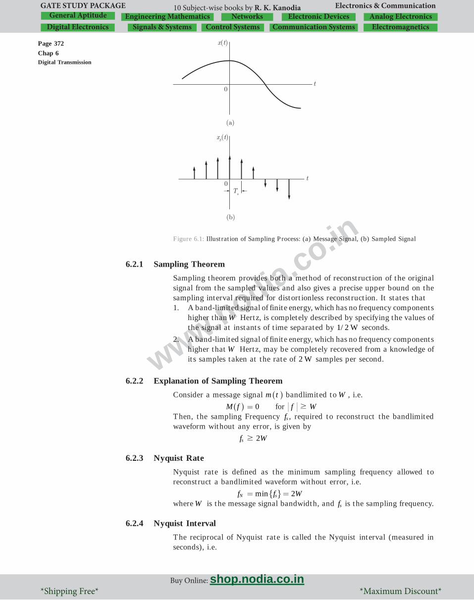
Page 372Chap 6Digital Transmission
www.nodia.co.in
GATE STUDY PACKAGE Electronics & Communication
Buy Online: shop.nodia.co.in *Shipping Free* *Maximum Discount*
10 Subject-wise books by R. K. KanodiaNetworks Electronic Devices Analog Electronics
Digital Electronics Signals & Systems Control Systems ElectromagneticsCommunication SystemsGeneral Aptitude Engineering Mathematics
Figure 6.1: Illustration of Sampling Process: (a) Message Signal, (b) Sampled Signal
6.2.1 Sampling Theorem
Sampling theorem provides both a method of reconstruction of the original signal from the sampled values and also gives a precise upper bound on the sampling interval required for distortionless reconstruction. It states that1. A band-limited signal of finite energy, which has no frequency components
higher than W Hertz, is completely described by specifying the values of the signal at instants of time separated by 1/2 W seconds.
2. A band-limited signal of finite energy, which has no frequency components higher that W Hertz, may be completely recovered from a knowledge of its samples taken at the rate of 2 W samples per second.
6.2.2 Explanation of Sampling Theorem
Consider a message signal m t^ h bandlimited to W , i.e.
M f^ h 0= for f W$Then, the sampling Frequency fs , required to reconstruct the bandlimited waveform without any error, is given by
fs W2$
6.2.3 Nyquist Rate
Nyquist rate is defined as the minimum sampling frequency allowed to reconstruct a bandlimited waveform without error, i.e.
fN 2min f Ws= =" ,
where W is the message signal bandwidth, and fs is the sampling frequency.
6.2.4 Nyquist Interval
The reciprocal of Nyquist rate is called the Nyquist interval (measured in seconds), i.e.

Page 373Chap 6
Digital Transmission
www.nodia.co.in
Buy Online: shop.nodia.co.in *Shipping Free* *Maximum Discount*
GATE STUDY PACKAGE Electronics & Communication
Sample Chapter of Communication System (Vol-9, GATE Study Package)
TN 1f W2
1N
= =
where fN is the Nyquist rate, and W is the message signal bandwidth.
6.3 PULSE MODULATION
Pulse modulation is the process of changing a binary pulse signal to represent the information to be transmitted. Pulse modulation can be either analog or digital.
6.3.1 Analog Pulse Modulation
Analog pulse modulation results when some attribute of a pulse varies continuously in one-to-one correspondence with a sample value. In analog pulse modulation systems, the amplitude, width, or position of a pulse can vary over a continuous range in accordance with the message amplitude at the sampling instant, as shown in Figure 6.2. These lead to the following three types of pulse modulation:1. Pulse Amplitude Modulation (PAM)
2. Pulse Width Modulation (PWM)
3. Pulse Position Modulation (PPM)
Figure 6.2: Representation of Various Analog Pulse Modulation
6.3.2 Digital Pulse Modulation
In systems utilizing digital pulse modulation, the transmitted samples take on only discrete values. Two important types of digital pulse modulation are:1. Delta Modulation (DM)
2. Pulse Code Modulation (PCM)

Page 374Chap 6Digital Transmission
www.nodia.co.in
GATE STUDY PACKAGE Electronics & Communication
Buy Online: shop.nodia.co.in *Shipping Free* *Maximum Discount*
10 Subject-wise books by R. K. KanodiaNetworks Electronic Devices Analog Electronics
Digital Electronics Signals & Systems Control Systems ElectromagneticsCommunication SystemsGeneral Aptitude Engineering Mathematics
In the following sections, we will discuss the various types of pulse modulation in some more detail.
6.4 PULSE AMPLITUDE MODULATION
Pulse amplitude modulation (PAM) is the conversion of the analog signal to a pulse-type signal in which the amplitude of the pulse denotes the analog information. PAM system utilizes two types of sampling: (1) Natural sampling and (2) Flat-top sampling.
6.4.1 Natural Sampling (Gating)
Consider an analog waveform m t^ h bandlimited to W hertz, as shown in Figure 6.3(a). The PAM signal that uses natural sampling (gating) is defined as
m ts ^ h m t s t= ^ ^h h
where s t^ h is the pulse waveform shown in Figure 6.3(b), and m ts ^ h is the resulting PAM signal shown in Figure 6.3(c)
Figure 6.3: Illustration of Nautural Sampling Pulse Amplitude Modulation: (a) Message Signal, (b) Pulse Waveform, (c) Resulting PAM Signal
6.4.2 Instantaneous Sampling (Flat-Top PAM)
Analog waveforms may also be converted to pulse signalling by the use of flat-top signalling with instantaneous sampling, as shown in Figure 6.4. If m t^ h is an analog waveform bandlimited to W hertz, the instantaneous sampled PAM signal is given by

Page 375Chap 6
Digital Transmission
www.nodia.co.in
Buy Online: shop.nodia.co.in *Shipping Free* *Maximum Discount*
GATE STUDY PACKAGE Electronics & Communication
Sample Chapter of Communication System (Vol-9, GATE Study Package)
m ts ^ h m kT h t kTs sk
= -3
3
=-^ ^h h/
where h t^ h denotes the sampling-pulse shape shown in Figure 6.4(b), and m ts ^ h is the resulting flat top PAM signal shown in Figure 6.4(c)
Figure 6.3: Illustration of Flat-top Sampling Pulse Amplitude Modulation: (a) Message Signal, (b) Sampling Pulse, (c) Resulting PAM Signal
POINT TO REMEMBER
The analog-to-PAM conversion process is the first step in converting an analog waveform to a PCM (digital) signal.
6.5 PULSE CODE MODULATION
Pulse code modulation (PCM) is essentially analog-to-digital conversion of a special type where the information contained in the instantaneous samples of an analog signal is represented by digital words in a serial bit stream. Figure 6.5 shows the basic elements of a PCM system. The PCM signal is generated by carrying out the following three basic operations:1. Sampling
2. Quantizing
3. Encoding
Figure 6.4 : Block Diagram Representation of PCM System

Page 376Chap 6Digital Transmission
www.nodia.co.in
GATE STUDY PACKAGE Electronics & Communication
Buy Online: shop.nodia.co.in *Shipping Free* *Maximum Discount*
10 Subject-wise books by R. K. KanodiaNetworks Electronic Devices Analog Electronics
Digital Electronics Signals & Systems Control Systems ElectromagneticsCommunication SystemsGeneral Aptitude Engineering Mathematics
6.5.1 Sampling
The incoming message signal m t^ h is sampled with a train of narrow rectangular pulses so as to closely approximate the instantaneous sampling process. To ensure perfect reconstruction of the message signal at the receiver, the sampling rate must be greater than twice the highest frequency component W of the message signal in accordance with the sampling theorem. The resulting sampled waveform m kTs^ h is discrete in time.
APPLICATION OF SAMPLING
The application of sampling permits the reduction of the continuously varying message signal (of some finite duration) to a limited number of discrete values per second.
6.5.2 Quantization
A quantizer rounds off the sample values to the nearest discrete value in a set of q quantum levels. The resulting quantized samples m kTq s^ h are discrete in time (by virtue of sampling) and discrete in amplitude (by virtue of quantizing). Basically, quantizers can be of a uniform or nonuniform type.
Figure 6.6: Representation of Relationship Between Sampled and Quantized Signal
Uniform Quantizer
A quantizer is called as a uniform quantizer if the step size remains constant throughout the input range. To display the relationship between m kTs^ h and m kTq s^ h, let the analog message be a voltage waveform normalized such that
1m t #^ h V . Uniform quantization subdivides the 2 V peak-to-peak range into q equal steps of height 2/q , as shown in Figure 6.6. The quantum levels are then taken to be at /q1! , /q3! ,..., /q q1! -^ h in the usual case when q is an even integer. A quantized value such as 5/m kT qq s =^ h corresponds to any sample value in the range / /q x xT q4 6< <s^ h .
Nonuniform Quantizer
Nonuniform quantization is required to be implemented to improve the signal to quantization noise ratio of weak signals. It is equivalent to passing the baseband signal through a compressor and then applying the compressed signal to a uniform quantizer. A particular form of compression law that is used in practice is the so called m-law, which is defined by

Page 377Chap 6
Digital Transmission
www.nodia.co.in
Buy Online: shop.nodia.co.in *Shipping Free* *Maximum Discount*
GATE STUDY PACKAGE Electronics & Communication
Sample Chapter of Communication System (Vol-9, GATE Study Package)
mq ln
ln m1
1m
m=
++^
`
h
j
where m and mq are the normalized input and output voltages, and m is a positive constant.
6.5.3 Encoding
An encoder translates the quantized samples into digital code words. The encoder works with M -ary digits and produces for each sample a code word consisting of n digits in parallel. Since, there are Mn possible M-ary codewords with n digits per word, unique encoding of the q different quantum levels requires that
Mn q$The parameters M , n , and q should be chosen to satisfy the equality, so that
q Mn= or n log qM=
Encoding in Binary PCM
For binary PCM, each digit may be either of two distinct values 0 or 1, i.e.
M 2=If the code word of binary PCM consists of n digits, then number of quantization levels is defined as
q 2n=or n log q2=In general, we must remember the following characteristics of a PCM system:
CHARACTERISTICS OF PCM SYSTEM
1. A sampled waveform is quantized into q quantization levels; where q is an integer.
2. If the message signal is defined in the range ,m mp p-^ h, then the step size of quantizer is
d 2qmp=
3. For a binary PCM system with n digit codes, the number of quantization level is defined as
q 2n=4. If the message signal is sampled at the sampling rate fs , and encoded
to n number of bits per sample; then the bit rate (bits/sec) of the PCM is defined as
Rb nfs=
METHODOLOGY 1 : TO EVALUATE BIT RATE FOR PCM SYSTEM
If the number of quantization levels q and message signal frequency fm for a PCM signal is given, then bit rate for the PCM system is obtained in the following steps:Step 1: Obtain the sampling frequency for the PCM signal. According to
Nyquist criterion, the minimum sampling frequency is given by
fs f2 m=

Page 378Chap 6Digital Transmission
www.nodia.co.in
GATE STUDY PACKAGE Electronics & Communication
Buy Online: shop.nodia.co.in *Shipping Free* *Maximum Discount*
10 Subject-wise books by R. K. KanodiaNetworks Electronic Devices Analog Electronics
Digital Electronics Signals & Systems Control Systems ElectromagneticsCommunication SystemsGeneral Aptitude Engineering Mathematics
Step 2: Deduce the number of bits per sample using the expression
n log q2=Step 3: Evaluate bit rate (bits/sec) for the PCM system by substituting
the obtained values in the expression
Rb nfs=
6.6 TRANSMISSION BANDWIDTH IN A PCM SYSTEM
The bandwidth of (serial) binary PCM waveforms depends on the bit rate and the waveform pulse shape used to represent the data. The dimensionality theorem shows that the bandwidth of the binary encoded PCM waveform is bounded by
BPCM R21
b$ nf21
s=
where Rb is the bit rate, n is the number of bits in PCM word, and fs is the sampling rate. Since, the required sampling rate for no aliasing is
fs 2W$where W is the bandwidth of the message signal (that is to be converted to the PCM signal). Thus, the bandwidth of the PCM signal has a lower bound given by
BPCM nW$
POINT TO REMEMBER
The minimum bandwidth of R nfs21
21= is obtained only when /sinx x^ h
type pulse shape is used to generate the PCM waveform. However, usually a more rectangular type of pulse shape is used, and consequently, the bandwidth of the binary-encoded PCM waveform will be larger than this minimum. Thus, for rectangular pulses, the first null bandwidth is
BPCM R= nfs= (first null bandwidth)
6.7 NOISE CONSIDERATION IN PCM
In PCM (pulse code modulation), there are two error sources:1. Quantization noise
2. Channel noise
6.7.1 Quantization Noise
For a PCM system, the k th sample of quantized message signal is represented by
m kTq s^ h m kT kTs se= +^ ^h h
where m kTs^ h is the sampled waveform, and kTse^ h is the quantization error. Let the quantization levels having uniform step size d . Then, we have
2d- 2# #e d
So, the mean-square error due to quantization is
2e d112/
/2
2
2 2
d e e d= =d
d
-# ...(6.1)

Page 379Chap 6
Digital Transmission
www.nodia.co.in
Buy Online: shop.nodia.co.in *Shipping Free* *Maximum Discount*
GATE STUDY PACKAGE Electronics & Communication
Sample Chapter of Communication System (Vol-9, GATE Study Package)
METHODOLOGY 2 : TO EVALUATE BIT RATE FOR PCM SYSTEM
For a PCM system, consider the message signal having frequency fm and peak to peak amplitude m2 p . If the accuracy of the PCM system is given as %x! of full scale value, then the bit rate is obtained in the following steps:Step 1 : Obtain the sampling frequency for the PCM signal. According
to Nyquist criterion, the minimum sampling frequency is given by
fs f2 m=Step 2 : Obtain the maximum quantization error for the PCM system
using the expression
error qm
qm m
2 22
2p p
npd = = = =
Step 3 : Apply the given condition of accuracy as
error % of full scale valuex#Step 4 : Solve the above condition for the minimum value of number of
bits per second n^ h.
Step 5 : Obtain the bit rate by substituting the approximated integer value of n in the expression
Rb nfs=
6.7.2 Signal to Quantization Noise Ratio
For PCM system, we have the message signal m t^ h, and quantization error e. So, we define the signal to quantization noise ratio as
SNR Q^ h /
m t m t122
2
2
2
e d= =^ ^h h
...(6.2)
where d is the step size of the quantized signal defined as
d qm2 p= ...(6.3)
Substituting equation (6.3) in equation (6.2), we get the expression for signal to quantization noise ratio as
SNR Q^ h 122 /m qm t
p2
2
=^
^
h
h
SNR Q^ h qm
m t3
p
22
2
= ^ h ...(6.4)
where mp is the peak amplitude of message signal m t^ h, and q is the number of quantization level. Let us obtain the more generalized form of SNR for the following two cases:
Case I :
When m t^ h is a sinusoidal signal, we have its mean square value
m t2^ h 1
2=and the peak amplitude of sinusoidal message signal is
mp 1=So, by substituting these values in equation (6.4), we get the signal to
quantization noise ratio for sinusoidal message signal as

Page 380Chap 6Digital Transmission
www.nodia.co.in
GATE STUDY PACKAGE Electronics & Communication
Buy Online: shop.nodia.co.in *Shipping Free* *Maximum Discount*
10 Subject-wise books by R. K. KanodiaNetworks Electronic Devices Analog Electronics
Digital Electronics Signals & Systems Control Systems ElectromagneticsCommunication SystemsGeneral Aptitude Engineering Mathematics
SNR Q^ h 31/ 3q q1 2
2
22
2= =^ h
Case II :
When m t^ h is uniformly distributed in the range ,m mp p-^ h, then we obtain
m t2^ h
m3
p2
=
Substituting this value in equation (6.4), we get the signal to quantization noise ratio as
SNR Q^ h /
qm
mq3
3p
p22
22= =
Case III:
For any arbitrary message signal m t^ h, the peak signal to quantization noise ratio is defined as
SNR peak^ h 3qmm
q3p
p22
22= =
6.7.3 Channel Noise
If a PCM signal is composed of the data that are transmitted over the channel having bit error rate Pe , then peak signal to average quantization noise ratio is defined as
SNR peak^ h 3q Pq
1 4 1
2
e2=
+ -^ hSimilarly, for the channel with bit error probability Pe , the average
signal to average quantization noise ratio is defined as
SNR ave^ h q Pq
1 4 1 e2
2
=+ -^ h
POINT TO REMEMBER
If the additive noise in the channel is so small that errors can be neglected, quantization is the only error source in PCM system.
6.7.4 Companding
Companding is nonuniform quantization. It is required to be implemented to improve the signal to quantization noise ratio of weak signals. The signal to quantization noise ratio for m-law companding is approximated as
SNR Q^ h 1ln
q32
2
m=
+^ h6 @
where q is the number of quantization level, and m is a positive constant.
6.8 ADVANTAGES OF PCM SYSTEM
PCM is very popular because of the many advantages it offers, including the following:1. Relatively inexpensive digital circuitry may be used extensively in the
system.
2. PCM signals derived from all types of analog sources (audio, video, etc.) may be merged with data signals (e.g., from digital computers) and transmitted over a common high-speed digital communication system.

Page 381Chap 6
Digital Transmission
www.nodia.co.in
Buy Online: shop.nodia.co.in *Shipping Free* *Maximum Discount*
GATE STUDY PACKAGE Electronics & Communication
Sample Chapter of Communication System (Vol-9, GATE Study Package)
3. In long-distance digital telephone systems requiring repeaters, a clean PCM waveform can be regenerated at the output of each repeater, where the input consists of a noisy PCM waveform.
4. The noise performance of a digital system can be superior to that of an analog system.
POINT TO REMEMBER
The advantages of PCM usually outweigh the main disadvantage of PCM: a much wider bandwidth than that of the corresponding analog signal.
6.9 DELTA MODULATION
Delta modulation provides a staircase approximation to the oversampled version of the message signal, as illustrated in Figure 6.7. Let m t^ h denote the input (message) signal, and m tq ^ h denote its staircase approximation. The difference between the input and the approximation is quantized into only two levels, namely, !d , corresponding to positive and negative differences. Thus if the approximation falls below the signal at any sampling approach, it is increased by d . If on the other hand, the approximation lies above the signal, it is diminished by d .
Figure 6.7: Staircase Approximation in Delta Modulation
Following are some key points related to delta modulation.
POINTS TO REMEMBER
1. In delta modulation (DM), an incoming message signal is oversampled (i.e. at a rate much higher than the Nyquist rate) to purposely increase the correlation between adjacent samples of the signal
2. The staircase approximation remains within !d of the input signal provided that the signal does not change too rapidly from sample to sample.
6.9.1 Noise Consideration in Delta Modulation
The quantizing noise error in delta modulation can be classified into two types of noise:1. Slope Overload Noise 2. Granular Noise

Page 382Chap 6Digital Transmission
www.nodia.co.in
GATE STUDY PACKAGE Electronics & Communication
Buy Online: shop.nodia.co.in *Shipping Free* *Maximum Discount*
10 Subject-wise books by R. K. KanodiaNetworks Electronic Devices Analog Electronics
Digital Electronics Signals & Systems Control Systems ElectromagneticsCommunication SystemsGeneral Aptitude Engineering Mathematics
1. Slope Overload Noise
Slope overload noise occurs when the step size d is too small for the accumulator output to follow quick changes in the input waveform. The maximum slope that can be generated by the accumulator output is
Ts
d fsd=where Ts is sampling interval, and fs is the sampling rate. To prevent the slope overload noise, the maximum slope of the message signal must be less than maximum slope generated by accumulator. Thus, we have the required condition to avoid slope overload as
max dtdm t^ h
fs# d
where m t^ h is the message signal, d is the step size of quantized signal, and fs is the sampling rate.
2. Granular Noise
The granular noise in a DM system is similar to the granular noise in a PCM system. From equation (6.1), we have the total quantizing noise for PCM system,
PCM2e^ h
/d1
12 32
/
/2
2
2 2 2
d e e d d= = =
d
d
-
^ h#Replacing /2d of PCM by d for DM, we obtain the total granular
quantizing noise as
DM2e^ h 3
2d=
Thus, the power spectral density for granular noise in delta modulation system is obtained as
S fN ^ h /f f23
6s s
2 2d d= =
where d is the step size, and fs is the sampling frequency.
POINT TO REMEMBER
Granular noise occurs for any step size but is smaller for a small step size. Thus we would like to have d as small as possible to minimize the granular noise.
METHODOLOGY : MINIMUM STEP SIZE IN DELTA MODULATION
Following are the steps involved in determination of minimum step size to avoid slope overload in delta modulation:Step 1: Obtain the sampling frequency for the modulation. According to
Nyquist criterion, the minimum sampling frequency is given by
fs f2 m=Step 2: Obtain the maximum slope of message signal using the expression
max dtdm t^ h
f A2 m mp =
where fm is the message signal frequency, and Am is amplitude of the message signal.

Page 383Chap 6
Digital Transmission
www.nodia.co.in
Buy Online: shop.nodia.co.in *Shipping Free* *Maximum Discount*
GATE STUDY PACKAGE Electronics & Communication
Sample Chapter of Communication System (Vol-9, GATE Study Package)
Step 3: Apply the required condition to avoid slope overload as
fsd max dtdm t
$^ h
Step 4: Evaluate the minimum value of step size d by solving the above condition.
6.10 MULTILEVEL SIGNALING
In a multilevel signaling scheme, the information source emits a sequence of symbols from an alphabet that consists of M symbols (levels). Let us understand some important terms used in multilevel signaling.
6.10.1 Baud
Let a multilevel signaling scheme having the symbol duration Ts seconds. So, we define the symbols per second transmitted for the system as
D T1s
=where D is the symbol rate which is also called baud.
6.10.2 Bits per Symbol
For a multilevel signaling scheme with M number of symbols (levels), we define the bits per symbol as
k log M2=
6.10.3 Relation Between Baud and Bit Rate
For a multilevel signaling scheme, the bit rate and baud (symbols per second) are related as
Rb logkD D M2= = ...(6.5)where Rb is the bit rate, logk M2= is the bits per symbol, and D is the baud (symbols per second).
6.10.4 Relation Between Bit Duration and Symbol Duration
For a multilevel signaling scheme, the bit duration is given by
Tb R1
b=
where Rb is the bit rate. Also, we have the symbol duration
Ts D1=
where D is the symbol rate. Thus, by substituting these expressions in equation (6.5), we get the relation
Ts logkT T Mb b 2= =where logk M2= is the bits per symbol.
6.10.5 Transmission Bandwidth
The null to null transmission bandwidth of the rectangular pulse multilevel waveform is defined as
BT D= symbols/secThe absolute transmission bandwidth for sin
xx pulse multilevel waveform is
defined as

Page 384Chap 6Digital Transmission
www.nodia.co.in
GATE STUDY PACKAGE Electronics & Communication
Buy Online: shop.nodia.co.in *Shipping Free* *Maximum Discount*
10 Subject-wise books by R. K. KanodiaNetworks Electronic Devices Analog Electronics
Digital Electronics Signals & Systems Control Systems ElectromagneticsCommunication SystemsGeneral Aptitude Engineering Mathematics
BT D2= symbols/sec
6.11 MULTIPLEXING
In many applications, a large number of data sources are located at a common point, and it is desirable to transmit these signals simultaneously using a single communication channel. This is accomplished using multiplexing. Let us study the two important types of multiplexing: FDM and TDM.
6.11.1 Frequency-Division Multiplexing (FDM)
Frequency-division multiplexing (FDM) is a technique whereby several message signals are translated, using modulation, to different spectral locations and added to form a baseband signal. The carriers used to form the baseband are usually referred to as subcarriers. Then, if desired, the baseband signal can be transmitted over a single channel using a single modulation process.
Bandwidth of FDM Baseband Signal
The bandwidth of FDM baseband is equal to the sum of the bandwidths of the modulated signals plus the sum of the guardbands, the empty spectral bands between the channels necessary for filtering. This bandwidth is lower-bounded by the sum of the bandwidths of the message signals, i.e.
B Wii
N
1
==/
where Wi is the bandwidth of m ti ^ h, This bandwidth is achieved when all baseband modulators are SSB and all guardbands have zero width.
6.11.2 Time Division Multiplexing (TDM)
Time-division multiplexing provides the time sharing of a common channel by a large number of users. Figure 6.8(a) illustrates a TDM system. The data sources are assumed to have been sampled at the Nyquist rate or higher. The commutator then interlaces the samples to form the baseband signal shown in Figure 6.8(b). At the channel output, the baseband signal is demultiplexed by using a second commutator as illustrated. Proper operation of this system depends on proper synchronization between the two commutators.

Page 385Chap 6
Digital Transmission
www.nodia.co.in
Buy Online: shop.nodia.co.in *Shipping Free* *Maximum Discount*
GATE STUDY PACKAGE Electronics & Communication
Sample Chapter of Communication System (Vol-9, GATE Study Package)
Figure 6.8: (a) Time Division Multiplexing System, (b) Resulting Baseband Signal
In a TDM system, the samples are transmitted depending on the message signal bandwidth. For example, let us consider the following two cases:1. If all message signals have equal bandwidth, then the samples are
transmitted sequentially, as shown in Figure 6.8(b).
2. If the sampled data signals have unequal bandwidths, more samples must be transmitted per unit time from the wideband channels. This is easily accomplished if the bandwidths are harmonically related. For example, assume that a TDM system has four data sources s t1^ h, s t2^ h
, s t3^ h, and s t4 ^ h having the bandwidths respectively as , , 2 ,W W W W4. Then, it is easy to show that a permissible sequence of baseband samples is a periodic sequence, one period of which is ... ....s s s s s s1 4 3 4 2 4
Bandwidth of TDM Baseband Signal
The minimum sampling bandwidth of a TDM baseband signal is defined as
B Wii
N
1
==/
where Wi is the bandwidth of the i th channel.
***********

Page 386Chap 6Digital Transmission
www.nodia.co.in
GATE STUDY PACKAGE Electronics & Communication
Buy Online: shop.nodia.co.in *Shipping Free* *Maximum Discount*
10 Subject-wise books by R. K. KanodiaNetworks Electronic Devices Analog Electronics
Digital Electronics Signals & Systems Control Systems ElectromagneticsCommunication SystemsGeneral Aptitude Engineering Mathematics
EXERCISE 6.1
Common Data For Q. 1 to 5 :Figure given below shows Fourier spectra of signal ( )x t and ( )y t .
MCQ 6.1.1 The Nyquist sampling rate for ( )x t is(A) 100 kHz (B) 200 kHz
(C) 300 kHz (D) 50 kHz
MCQ 6.1.2 The Nyquist sampling rate for ( )y t is(A) 50 kHz (B) 75 kHz
(C) 150 kHz (D) 300 kHz
MCQ 6.1.3 The Nyquist sampling rate for ( )x t2 is(A) 100 kHz (B) 150 kHz
(C) 250 kHz (D) 400 kHz
MCQ 6.1.4 The Nyquist sampling rate for ( )y t3 is(A) 100 kHz (B) 300 kHz
(C) 900 kHz (D) 120 kHz
MCQ 6.1.5 The Nyquist sampling rate for ( ) ( )x t y t is(A) 250 kHz (B) 500 kHz
(C) 50 kHz (D) 100 kHz
Common Data For Q. 6 and 7A signal ( )x t is multiplied by rectangular pulse train ( )c t shown in figure.
MCQ 6.1.6 ( )x t would be recovered from the product ( ) ( )x t c t by using an ideal LPF if ( ) 0X jw = for

Page 387Chap 6
Digital Transmission
www.nodia.co.in
Buy Online: shop.nodia.co.in *Shipping Free* *Maximum Discount*
GATE STUDY PACKAGE Electronics & Communication
Sample Chapter of Communication System (Vol-9, GATE Study Package)
(A) 2000> pw (B) 1000> pw(C) 1000< pw (D) 2000< pw
MCQ 6.1.7 If ( )X jw satisfies the constrains required, then the pass band gain A of the ideal lowpass filter needed to recover ( )x t from ( ) ( )c t x t is(A) 1 (B) 2
(C) 4 (D) 8
Common Data For Q. 8 and 9 :Ten telemetry signals, each of bandwidth 2 kHz, are to be transmitted simultaneously by binary PCM. The maximum tolerable error in sample amplitudes is 0.2% of the peak signal amplitude. The signals must be sampled at least 20% above the Nyquist rate. Framing and synchronizing requires an additional 1% extra bits.
MCQ 6.1.8 The minimum possible data rate must be(A) 272.64 k bits/sec
(B) 436.32 k bits/sec
(C) 936.32 k bits/sec
(D) None of the above
MCQ 6.1.9 The minimum transmission bandwidth is(A) 218.16 kHz (B) 468.32 kHz
(C) 136.32 kHz (D) None of the above
MCQ 6.1.10 A binary channel with capacity 36 k bits/sec is available for PCM voice transmission. If signal is band limited to 3.2 kHz, then the appropriate values of quantizing level and the sampling frequency will be, respectively(A) 32, 3.6 kHz (B) 64, 7.2 kHz
(C) 64, 3.6 kHz (D) 32, 7.2 kHz
Common Data For Q. 11 to 13 :Consider a linear DM system designed to accommodate analog message signals limited to bandwidth of 3.5 kHz. A sinusoidal test signal of amplitude
1Am = V and frequency 800fm = Hz is applied to system. The sampling rate of the system is 64 kHz.
MCQ 6.1.11 The minimum value of the step size to avoid slope overload is(A) 240 mV (B) 120 mV
(C) 670 mV (D) 78.5 mV
MCQ 6.1.12 The granular-noise power would be(A) 1.68 10 3
#- W (B) 2.86 10 4
#- W
(C) 2.48 10 3#
- W (D) 1.12 10 4#
- W
MCQ 6.1.13 The SNR will be(A) 298 (B) 1.75 10 3
#-
(C) 4.46 103# (D) 201

Page 388Chap 6Digital Transmission
www.nodia.co.in
GATE STUDY PACKAGE Electronics & Communication
Buy Online: shop.nodia.co.in *Shipping Free* *Maximum Discount*
10 Subject-wise books by R. K. KanodiaNetworks Electronic Devices Analog Electronics
Digital Electronics Signals & Systems Control Systems ElectromagneticsCommunication SystemsGeneral Aptitude Engineering Mathematics
Common Data For Q. 14 and 15 :A Signal has a bandwidth of 1 MHz. It is sampled at a rate 50% higher than the Nyquist rate and quantized into 256 level using a m-law quantizer with
2 55m = .
MCQ 6.1.14 The signal-to-quantization-noise ratio is(A) 34.91 dB (B) 38.06 dB
(C) 42.05 dB (D) 48.76 dB
MCQ 6.1.15 It was found that a sampling rate 20% above the rate would be adequate. So the maximum SNR, that can be realized without increasing the transmission bandwidth, would be(A) 64.4 dB (B) 70.3 dB
(C) 50.1 dB (D) None of the above
MCQ 6.1.16 The input to a linear delta modulator having step-size 0.628d = is a sine wave with frequency fm and peak amplitude Am . If the sampling frequency
40fs = kHz, the combination of the sine wave frequency and the peak amplitude, where slope overload will take place is
Am fm(A) 0.3 V 8 kHz
(B) 1.5 V 4 kHz
(C) 1.5 V 2 kHz
(D) 3.0 V 1 kHz
MCQ 6.1.17 A sinusoidal signal is sampled at 8 kHz and is quantized using 8 bit uniform quantizer. If SNRq be the quantization signal to noise ratio and R be the bit rate of PCM signal, which of the following provides the correct values of SNRq and R ?(A) 32R = kbps, 25.8SNRq = dB
(B) 64R = kbps, 49.8SNRq = dB
(C) 64R = kbps, 55.8SNRq = dB
(D) 32R = kbps, 49.8SNRq = dB
MCQ 6.1.18 A 1.0 kHz signal is flat-top sampled at the rate of 1800 samples/sec and the samples are applied to an ideal rectangular LPF with cut-off frequency of 1100 Hz. The output of the filter contains(A) only 800 Hz component
(B) 800 and 900 Hz component
(C) 800 Hz and 1000 Hz components
(D) 800 Hz, 900 and 1000 Hz components
MCQ 6.1.19 A signal ( ) 100 (24 10 )cosx t t3p #= is ideally sampled with a sampling period of 50 secm and then passed through an ideal lowpass filter with cutoff frequency of 15 kHz. Which of the following frequencies is/are present at the filter output(A) 12 kHz only (B) 8 kHz only
(C) 12 kHz and 9 kHz (D) 12 kHz and 8 kHz

Page 389Chap 6
Digital Transmission
www.nodia.co.in
Buy Online: shop.nodia.co.in *Shipping Free* *Maximum Discount*
GATE STUDY PACKAGE Electronics & Communication
Sample Chapter of Communication System (Vol-9, GATE Study Package)
MCQ 6.1.20 The minimum sampling frequency (in samples/sec) required to reconstruct the following signal form its samples without distortion would be
( )x t 5 2 1000 7 2 1000sin sint
tt
t3 2
pp
pp= +b bl l
(A) 2 103# Hz (B) 4 103
# Hz
(C) 6 103# Hz (D) 8 103
# Hz
MCQ 6.1.21 The minimum step-size required for a Delta-Modulator operating at 32 K samples/sec to track the signal (here ( )u t is the unit function)
( )m t
125 [ ( ) ( 1)] (250 125 )[ ( 1) ]t u t u t t u t u t 2= - - + - - - -^ hso that slope overload is avoided, would be(A) 2 10- (B) 2 8-
(C) 2 6- (D) 2 4-
MCQ 6.1.22 If the number of bits in a PCM system is increased from n to 1n + , the signal-to-quantization noise ratio will increase by a factor.
(A) ( )
nn 1+
(B) ( )
nn 1
2
2+
(C) 2 (D) 4
MCQ 6.1.23 In PCM system, if the quantization levels are increased form 2 to 8, the relative bandwidth requirement will.(A) remain same
(B) be doubled
(C) be tripled
(D) become four times
Common Data For Q. 24 to 26 :A singer’s performance is to be recorded by sampling and storing the sample values. Assume that the highest frequency tone to be recorded is 15800 hertz.
MCQ 6.1.24 What is the minimum sampling frequency that can be used ?(A) 3.16 10 Hz4
# (B) 15.8 10 Hz4#
(C) 7.9 10 Hz3# (D) 6.32 10 Hz4
#
MCQ 6.1.25 How many samples would be required to store a three minutes performance ?(A) .1 053 104
# samples
(B) .5 688 106# samples
(C) .1 756 106# samples
(D) .9 48 104# samples
MCQ 6.1.26 If each sample is quantized into 128 levels, how many binary digits (bits) would be required to store the three minutes performance ?(A) .8 125 105
# bits (B) .7 28 108# bits
(C) .3 98 107# bits (D) .5 688 106
# bits
PROBLEM SOLVER/597/11.6
PROBLEM SOLVER/597/11.6
PROBLEM SOLVER/597/11.6

Page 390Chap 6Digital Transmission
www.nodia.co.in
GATE STUDY PACKAGE Electronics & Communication
Buy Online: shop.nodia.co.in *Shipping Free* *Maximum Discount*
10 Subject-wise books by R. K. KanodiaNetworks Electronic Devices Analog Electronics
Digital Electronics Signals & Systems Control Systems ElectromagneticsCommunication SystemsGeneral Aptitude Engineering Mathematics
Common Data For Q. 27 and 28 :A voltage of 1 volt rms is applied at the sending end of a telephone cable of length 1000 meters. The attenuation in the cable is 1 dB/m.
MCQ 6.1.27 What will be the rms voltage at receiving end of the cable ?(A) 10 volt50 (B) 10 volt50-
(C) 10 volt5 (D) 10 5- volt
MCQ 6.1.28 It is desired to obtain a 1 volt rms signal at the receiving end. This can be accomplished by using repeaters. If the repeaters yield a maximum output of 1 volt and have a voltage gain of 100, then the number of repeaters needed is(A) 100 (B) 25
(C) 5 (D) 40
Common Data For Q. 29 to 31 :The probability density of a signal X t^ h is given by
f xX t ^^ hh 4
0
for volt
otherwise
ke Xx #=
-
*
MCQ 6.1.29 If the signal X t^ h is quantized into 4 levels, what will be the step size of each level ?(A) 2 volt (B) 8 volt
(C) 32 volt (D) 1 volt
MCQ 6.1.30 What will be the value of constant k ?(A) .9 16 10 3
#- (B) 0.4908
(C) 27.29 (D) 0.5093
MCQ 6.1.31 If the probability density function is not constant over each level, what will be the variance of the quantization error ?(A) 0.1869 (B) 0.5093
(C) 0.7341 (D) 0.3739
MCQ 6.1.32 Consider the two message signals defined as
m t1^ h sin c t100= ^ h, sin cm t t10022=^ ^h h
what are the values of Nyquist rates fN1 and fN 2 of the corresponding signals ?
fN1 fN 2
(A) 100 200
(B) 200 100
(C) 50 100
(D) 100 50
MCQ 6.1.33 In a binary system, the quantizing noise is not to exceed %x! of the peak-to-peak analog level. The minimum number of bits in each PCM words needs to be(A) /x 50 (B) 50/x
(C) log x50
2b l (D) log x502a k
PROBLEM SOLVER/597/11.6
PROBLEM SOLVER/597/11.6
PROBLEM SOLVER/626/12.2
PROBLEM SOLVER/626/12.2
PROBLEM SOLVER/626/12.2
CARTOON/255/6.1.20
COUCH/250/3.7

Page 391Chap 6
Digital Transmission
www.nodia.co.in
Buy Online: shop.nodia.co.in *Shipping Free* *Maximum Discount*
GATE STUDY PACKAGE Electronics & Communication
Sample Chapter of Communication System (Vol-9, GATE Study Package)
Common Data For Q. 34 and 35 :The information in an analog voltage waveform is to be transmitted over a PCM system with a . %0 1! accuracy. The analog waveform has an absolute bandwidth of 100 Hz and an amplitude range of 10 V- to 10 V+ .
MCQ 6.1.34 What is the minimum sampling rate needed for the waveform ?(A) 102 Hz (B) 100 Hz
(C) 200 Hz (D) 50 Hz
MCQ 6.1.35 What is the minimum absolute channel bandwidth required for transmission of this PCM ?(A) 1800 Hz (B) 900 Hz
(C) 450 Hz (D) 3600 Hz
MCQ 6.1.36 An 850 Mbyte hard disk is used to store PCM data. Suppose that a voice frequency signal is sampled at 8 k samples/sec and the encoded PCM is to have an average SNR of at least 30 dB. How many minutes of voice frequency conversation can be stored on the hard disk ?(A) 2.833 minute (B) 170 103
# minute
(C) 2833 minute (D) 1700 minute
Common Data For Q. 37 and 38 :An analog signal with a bandwidth of 4.2 MHz is to be converted into binary PCM and transmitted over a channel. The peak signal quantizing noise ratio must be at least 55 dB.
MCQ 6.1.37 If there is no bit error and no inter symbol interferrence, what will be the number of quantizing steps needed ?(A) 512 (B) 9
(C) 4 (D) 256
MCQ 6.1.38 What will be the channel bandwidth required if rectangular pulse shapes are used ?(A) 75.6 MHz (B) 8.4 MHz
(C) 933.3 kHz (D) 17.4 MHz
Common Data For Q. 39 and 40 :Compact disk (CD) players use 16 bit PCM, including one parity bit with 8 times oversampling of the analog signal. The analog signal bandwidth is 20 kHz.
MCQ 6.1.39 What is the null bandwidth of this PCM signal ?(A) 640 MHz (B) 320 kHz
(C) 512 MHz (D) 512 MHz
MCQ 6.1.40 What will be the peak SNR for the signal ?(A) 9.50 dB (B) 10.1 dB
(C) 95.08 dB (D) 101.1 dB
COUCH/250/3.8
COUCH/250/3.8
COUCH/250/3.9
COUCH/250/3.10
COUCH/250/3.10
COUCH/250/3.11 (A,B)
COUCH/250/3.11 (A,B)

Page 392Chap 6Digital Transmission
www.nodia.co.in
GATE STUDY PACKAGE Electronics & Communication
Buy Online: shop.nodia.co.in *Shipping Free* *Maximum Discount*
10 Subject-wise books by R. K. KanodiaNetworks Electronic Devices Analog Electronics
Digital Electronics Signals & Systems Control Systems ElectromagneticsCommunication SystemsGeneral Aptitude Engineering Mathematics
Common Data For Q. 41 and 42 :In a PCM system, the bit error rate due to channel noise is 10 4- . Assume that the peak signal to noise ratio on the recovered analog signal needs to be at least 30 dB.
MCQ 6.1.41 What is the minimum number of quantizing steps that can be used to encode the analog signal into a PCM signal ?(A) 32 (B) 16
(C) 64 (D) 8
MCQ 6.1.42 If the original analog signal had an absolute bandwidth of 2.7 kHz, what is the null bandwidth of the PCM signal ?(A) 27 kHz (B) 13.5 kHz
(C) 10.4 kHz (D) 5.4 kHz
Common Data For Q. 43 to 45 :A multi level digital communication system sends one of 16 possible levels over the channel every 0.8 ms.
MCQ 6.1.43 What is the number of bits corresponding to each level ?(A) 16 bits/level
(B) 2 bits/level
(C) 4 bits/level
(D) 8 bits/level
MCQ 6.1.44 What is the baud rate ?(A) 8 baud
(B) 8000 baud
(C) 1250 baud
(D) 1.25 baud
MCQ 6.1.45 What is the bit rate for the signal ?(A) 5 k bits/sec (B) 1.25 k bits/sec
(C) 0.31 k bits/sec (D) 4 k bits/sec
Common Data For Q. 46 to 48 :The information in an analog waveform is first encoded into binary PCM and then converted to a multilevel signal for transmission over the channel. The number of multilevels is eight. Assume that analog signal has a bandwidth of 2700 Hz and is to be reproduced at the receiver output with an accuracy of %1! (full scale)
MCQ 6.1.46 What is the minimum bit rate of the PCM signal ?(A) 900 bits/sec
(B) 32.4 k bits/sec
(C) 6 k bits/sec
(D) 1.11 k bits/sec
COUCH/251/3.14 (A,B)
COUCH/251/3.14 (A,B)
COUCH/251/3.19
COUCH/251/3.19
COUCH/251/3.19
COUCH/253/3.34

Page 393Chap 6
Digital Transmission
www.nodia.co.in
Buy Online: shop.nodia.co.in *Shipping Free* *Maximum Discount*
GATE STUDY PACKAGE Electronics & Communication
Sample Chapter of Communication System (Vol-9, GATE Study Package)
MCQ 6.1.47 The minimum baud rate of the multilevel signal is(A) 97.2 k symbols/sec
(B) 32.4 k symbols/sec
(C) 4.05 k symbols/sec
(D) 10.8 k symbols/sec
MCQ 6.1.48 What is the minimum absolute channel bandwidth required for transmission of the PCM signal ?(A) 10.8 kHz
(B) 5.4 kHz
(C) 12.8 kHz
(D) 21.6 kHz
Common Data For Q. 49 and 50 :A binary waveform of 9600 bits/sec is converted into an octal (multilevel) waveform that is passed through a channel with a raised cosine roll of Nyquist filter characteristic. The channel has a conditioned phase response out to 2.4 kHz.
MCQ 6.1.49 What is the baud rate of the multilevel signal ?(A) 3 k symbol/sec
(B) 28.8 k symbol/sec
(C) 3.2 k symbol/sec
(D) 9.6 k symbol/sec
MCQ 6.1.50 What is the roll off factor of the filter characteristic ?(A) 2 (B) 0.5
(C) 3 (D) 1
Common Data For Q. 51 and 52 :An analog signal is to be converted into PCM signal that is a binary polar NRZ line code. The signal is transmitted over a channel that is absolutely bandlimited to 4 kHz. Assume that the PCM quantizer has 16 steps and that the overall equivalent system transfer function is of the raised cosine roll off type with roll off factor .0 5a = .
MCQ 6.1.51 What is the maximum PCM bit rate that can be supported by this system without introducing ISI (intersymbol interference) ?(A) 5.33 k bits/sec
(B) 8 k bits/sec
(C) 12 k bits/sec
(D) 16 k bits/sec
MCQ 6.1.52 The maximum bandwidth that can be permitted for the analog signal is(A) 666 Hz
(B) 2.22 kHz
(C) 333 Hz
(D) 1.33 kHz
COUCH/253/3.34
COUCH/253/3.34
COUCH/253/3.35(A,B)
COUCH/253/3.35(A,B)
COUCH/254/3.45
COUCH/254/3.45

Page 394Chap 6Digital Transmission
www.nodia.co.in
GATE STUDY PACKAGE Electronics & Communication
Buy Online: shop.nodia.co.in *Shipping Free* *Maximum Discount*
10 Subject-wise books by R. K. KanodiaNetworks Electronic Devices Analog Electronics
Digital Electronics Signals & Systems Control Systems ElectromagneticsCommunication SystemsGeneral Aptitude Engineering Mathematics
Common Data For Q. 53 and 54 :Multilevel data with an equivalent bit rate of 2400 bits/sec is sent over a channel using a four level line code that has a rectangular pulse shape at the output of the transmitter. The overall transmission system (i.e., the transmitter, channel and receiver) has an .0 5a = raised cosine roll off Nyquist filter characteristic.
MCQ 6.1.53 What is the 6 dB bandwidth for this transmission system ?(A) 2400 Hz (B) 1200 Hz
(C) 300 Hz (D) 600 Hz
MCQ 6.1.54 What is the absolute bandwidth for the system ?(A) 900 Hz (B) 1800 Hz
(C) 450 Hz (D) 600 Hz
Common Data For Q. 55 to 57 :A DM (Delta modulation) system is tested with a 10 kHz sinusoidal signal, 1 volt peak-to-peak, at the input. The signal is sampled at 10 times the Nyquist rate.
MCQ 6.1.55 What is the minimum step size required to prevent slope overload ?(A) 0.157 volt (B) 0.314 volt
(C) 0.05 volt (D) 0.1 volt
MCQ 6.1.56 What is the power spectral density for the granular noise ?(A) 1.23 10 /V Hz7 2
#- (B) 2.47 10 /V Hz2 2
#-
(C) 7.39 10 /V Hz7 2#
- (D) 2.06 10 /V Hz8 2#
-
MCQ 6.1.57 If the receiver input is band limited to 200 kHz, what is the average signal quantizing noise power ratio ?(A) 11.8 dB (B) 1.18 dB
(C) 14.8 dB (D) 1.48 dB
MCQ 6.1.58 Five messages bandlimited to W , W , W2 , W4 and W4 Hz, respectively are to be time division multiplexed. What is the minimum transmission bandwidth required for this TDM signal ?(A) W24 (B) W
(C) W4 (D) W12
***********
COUCH/255/3.47
COUCH/255/3.47
COUCH/255/3.50
COUCH/255/3.50
COUCH/255/3.50
ZEIMER/192/3.59

Page 395Chap 6
Digital Transmission
www.nodia.co.in
Buy Online: shop.nodia.co.in *Shipping Free* *Maximum Discount*
GATE STUDY PACKAGE Electronics & Communication
Sample Chapter of Communication System (Vol-9, GATE Study Package)
EXERCISE 6.2
QUES 6.2.1 Consider a set of 10 signals ( ),x ti 1,2,3, ...10i = . Each signal is band limited to 1 kHz. All 10 signals are to be time-division multiplexed after each is multiplied by a carrier ( )c t shown in figure.
If the period Ts of ( )c t is chosen that have the maximum allowable value, the largest value of 3 would be _______ sm .
QUES 6.2.2 A compact disc recording system samples a signal with a 16-bit analog-to-digital convertor at 44.1 kHz. The CD can record an hour worth of music. The approximate capacity of CD is _______ Mbytes.
QUES 6.2.3 An analog signal is sampled at 36 kHz and quantized into 256 levels. The time duration of a bit of the binary coded signal is _______ sm .
QUES 6.2.4 An analog signal is quantized and transmitted using a PCM system. The tolerable error in sample amplitude is 0.5% of the peak-to-peak full scale value. The minimum binary digits required to encode a sample is _______
QUES 6.2.5 A Television signal is sampled at a rate of 20% above the Nyquist rate. The signal has a bandwidth of 6 MHz. The samples are quantized into 1024 levels. The minimum bandwidth required to transmit this signal would be _______ Mbps.
QUES 6.2.6 A CD record audio signals digitally using PCM. The audio signal bandwidth is 15 kHz. The Nyquist samples are quantized into 32678 levels and then binary coded. What is the minimum bit rate (in kbps) required to encode the audio signal ?
QUES 6.2.7 The American Standard Code for information interchange has 128 characters, which are binary coded. If a certain computer generates 1,000,000 character per second, the minimum bandwidth required to transmit this signal will be _______ Mbps.
QUES 6.2.8 Figure given below shows a PCM signal in which amplitude level of + 1 volt

Page 396Chap 6Digital Transmission
www.nodia.co.in
GATE STUDY PACKAGE Electronics & Communication
Buy Online: shop.nodia.co.in *Shipping Free* *Maximum Discount*
10 Subject-wise books by R. K. KanodiaNetworks Electronic Devices Analog Electronics
Digital Electronics Signals & Systems Control Systems ElectromagneticsCommunication SystemsGeneral Aptitude Engineering Mathematics
and - 1 volt are used to represent binary symbol 1 and 0 respectively. The code word used consists of three bits. The sampled version of analog signal from which this PCM signal is derived is _______
QUES 6.2.9 A PCM system uses a uniform quantizer followed by a 8-bit encoder. The bit rate of the system is equal to 108 bits/s. The maximum message bandwidth for which the system operates satisfactorily is _______ MHz.
QUES 6.2.10 Twenty-four voice signals are sampled uniformly at a rate of 8 kHz and then time-division multiplexed. The sampling process uses flat-top samples with 1 sm duration. The multiplexing operation includes provision for synchronization by adding an extra pulse of 1 sm duration. What is the spacing (in sm ) between successive pulses of the multiplexed signal ?
QUES 6.2.11 A linear delta modulator is designed to operate on speech signals limited to 3.4 kHz. The sampling rate is 10 times the Nyquist rate of the speech signal. The step size d is 100 mV. The modulator is tested with a 1kHz sinusoidal test signal. The maximum amplitude of the test signal required to avoid slope overload is _______ mV.
QUES 6.2.12 The output signal-to-quantization-noise ratio of a 10-bit PCM was found to be 30 dB. The desired SNR is 42 dB. It can be increased by increasing the number of quantization level. In this way the percentage increase in the transmission bandwidth would be _______ %. (Assume 10 0.3log2 = )
QUES 6.2.13 For a PCM signal the compression parameter 100m = and the minimum signal to quantization-noise ratio is 50 dB. The number of bits per sample would be _______
QUES 6.2.14 A sinusoid massage signal ( )m t is transmitted by binary PCM without compression. If the signal to-quantization-noise ratio is required to be at least 48 dB, the minimum number of bits per sample will be _______
QUES 6.2.15 A speech signal has a total duration of 20 sec. It is sampled at the rate of 8 kHz and then PCM encoded. The signal-to-quantization noise ratio is required to be 40 dB. The minimum storage capacity needed to accommodate this signal is _______ kbytes.
QUES 6.2.16 A sinusoidal signal with peak-to-peak amplitude of 1.536 V is quantized into 128 levels using a mid-rise uniform quantizer. The quantization-noise power is _______ V10 6 2
#- .

Page 397Chap 6
Digital Transmission
www.nodia.co.in
Buy Online: shop.nodia.co.in *Shipping Free* *Maximum Discount*
GATE STUDY PACKAGE Electronics & Communication
Sample Chapter of Communication System (Vol-9, GATE Study Package)
QUES 6.2.17 The Nyquist sampling interval, for the signal (700 ) (500 )sin sinc ct t+ is _______ second.
QUES 6.2.18 In a PCM system, if the code word length is increased form 6 to 8 bits, then by what factor signal to quantization noise ratio improves ?
QUES 6.2.19 Four signals ( ), ( ), ( )g t g t g t1 2 3 and ( )g t4 are to be time division multiplexed and transmitted. ( )g t1 and ( )g t4 have a bandwidth of 4 kHz, and the remaining two signals have bandwidth of 8 kHz. Each sample requires 8 bits for encoding. What is the minimum transmission bit rate (kbps) of the system ?
QUES 6.2.20 Three analog signals, having bandwidths 1200 Hz, 600 Hz and 600 Hz, are sampled at their respective Nyquist rates, encoded with 12 bit words, and time division multiplexed. What is the bit rate (in kbps) for the multiplexed signal ?
QUES 6.2.21 Four signals each band limited to 5 kHz are sampled at twice the Nyquist rate. The resulting PAM samples are transmitted over a single channel after time division multiplexing. The theoretical minimum transmission bandwidth of the channel should be equal to _______ kHz.
QUES 6.2.22 Four independent messages have bandwidths of 100 Hz, 100 Hz, 200 Hz and 400 Hz respectively. Each is sampled at the Nyquist rate, time division multiplexed and transmitted. The transmitted sample rate in Hz, is given by _______
QUES 6.2.23 The Nyquist sampling rate for the signal ( )g t 10 (50 ) (150 )cos cost t2p p= where ' 't is in seconds, is _______ samples per second.
QUES 6.2.24 A TDM link has 20 signal channels and each channel is sampled 8000 times/sec. Each sample is represented by seven binary bits and contains an additional bit for synchronization. The total bit rate for the TDM link is _______ kbps.
QUES 6.2.25 The Nyquist sampling interval for the signal ( )s t (350 ) (250 )sin sinc ct t= + is _______ second.
QUES 6.2.26 In a CD player, the sampling rate is 44.1 kHz and the samples are quantized using a 16-bit/sample quantizer. The resulting number of Mega-bits for a piece of music with a duration of 50 minutes is _______
QUES 6.2.27 Four voice signals, each limited to 4 kHz and sampled at Nyquist rate are converted into binary PCM signal using 256 quantization levels. The bit transmission rate for the time-division multiplexed signal will be _______ kbps.

Page 398Chap 6Digital Transmission
www.nodia.co.in
GATE STUDY PACKAGE Electronics & Communication
Buy Online: shop.nodia.co.in *Shipping Free* *Maximum Discount*
10 Subject-wise books by R. K. KanodiaNetworks Electronic Devices Analog Electronics
Digital Electronics Signals & Systems Control Systems ElectromagneticsCommunication SystemsGeneral Aptitude Engineering Mathematics
QUES 6.2.28 Analog data having highest harmonic at 30 kHz generated by a sensor has been digitized using 6 level PCM. What will be the rate (in kbps) of digital signal generated ?
QUES 6.2.29 In a PCM system, the number of quantization levels is 16 and the maximum signal frequency is 4 kHz; the bit transmission rate is _______ kbps.
QUES 6.2.30 A speech signal occupying the bandwidth of 300 Hz to 3 kHz is converted into PCM format for use in digital communication. If the sampling frequency is 8 kHz and each sample is quantized into 256 levels, then the output bit rate will be _______ kbps.
QUES 6.2.31 A PCM system is time division multiplexed with a data source, as shown in figure below. The output of the time division multiplexer is fed into a PSK modulator after which the signal is transmitted over a channel of bandwidth
1MHzBT = with center frequency at 100 MHz. What is the maximum number of quantization levels required in this system ?
QUES 6.2.32 A time division multiplexing system using PCM is used to multiplex telephone conversations over a single communication channel. It is found that a minima interval of 1 sm must be allowed for reliable identification of bits at the receiving end. If the allowable voice bandwidth for telephone line transmission is 3 kHz and the quantization level is given as 16, what is the approximate number of voice signals that can be multiplexed ?
Common Data For Q. 33 and 34 :Consider a PCM multiplexing system using a 256 level signal quantizer for the transmission of three signals m1, m2 and m3, bandlimited to 5 kHz, 10 kHz, and 5 kHz, respectively. Assume that each signal is sampled at Nyquist rate and 8 bits transmitted simultaneously.
PROBLEM SOLVER/643/12.13
PROBLEM SOLVER/644/12.14

Page 399Chap 6
Digital Transmission
www.nodia.co.in
Buy Online: shop.nodia.co.in *Shipping Free* *Maximum Discount*
GATE STUDY PACKAGE Electronics & Communication
Sample Chapter of Communication System (Vol-9, GATE Study Package)
QUES 6.2.33 What is the maximum bit duration (in sm ) for the transmitted signal ?
QUES 6.2.34 The channel bandwidth required to pass the PCM signal is _______ kHz.
QUES 6.2.35 An information signal to be transmitted digitally is a rectangular wave with a period of 71.4 sm . It has been determined that the wave will be adequately passed if the bandwidth includes the fourth harmonic. The minimum sampling frequency required for the signal is _______ kHz.
QUES 6.2.36 The voltage range of an A/D converter that uses 14 bit numbers is 6- to 6 V+ . What will be the resolution (in Vm ) of digitization ?
QUES 6.2.37 The input voltage of a compander with a maximum voltage range of 1 volt and 255m = is 0.25 volt. What will be the voltage gain of compander ?
QUES 6.2.38 A multilevel digital communication system is to operate at a data rate of 9600 bits/sec. If 4 bit words are encoded into each level for transmission over the channel, what is the minimum required bandwidth (in Hz) for the channel ?
QUES 6.2.39 An analog signal is to be converted into a PCM signal that is multilevel polar NRZ line code with four number of levels. The signal is transmitted over a channel that is absolutely bandlimited to 4 kHz. Assume that the PCM quantizer has 16 steps and that the overall equivalent system transfer function is of the raised cosine roll off type with roll off factor .0 5a = . What is the maximum bandwidth (in kHz) that can be permitted for the analog signal ?
QUES 6.2.40 Assume that a PCM type system is to be designed such that an audio signal can be delivered at the receiver output. The audio signal is to have a bandwidth of 3400 Hz and an SNR of at least 40 dB. What is the bit rate requirement (in kbps) for a design that uses 255m = companded PCM signaling ?
QUES 6.2.41 A continuous data signal is quantized and transmitted using a PCM signal. If each data sample at the receiving end of the system must be known to within . %0 5! of the peak-to-peak full scale value, how many binary symbols must each transmitted digital word contain ?
QUES 6.2.42 A delta modulator has the message signal,
m t^ h sin sint t4 2 10 5 2 20p p= +^ ^h h
If the step size is .0 05d p= , what is the minimum sampling frequency (in Hz) required to prevent slope overload ?
PROBLEM SOLVER/645/12.15
PROBLEM SOLVER/645/12.15
FRENZEL/210/7.1(C)
FRENZEL/222/7.2
FRENZEL/233/7.4
COUCH/251/3.20(A)
COUCH/254/3.46
COUCH/255/3.48(A)
ZEIMER/192/3.56
ZEIMER/192/3.58

Page 400Chap 6Digital Transmission
www.nodia.co.in
GATE STUDY PACKAGE Electronics & Communication
Buy Online: shop.nodia.co.in *Shipping Free* *Maximum Discount*
10 Subject-wise books by R. K. KanodiaNetworks Electronic Devices Analog Electronics
Digital Electronics Signals & Systems Control Systems ElectromagneticsCommunication SystemsGeneral Aptitude Engineering Mathematics
QUES 6.2.43 A message signal has the following frequency components :First component : A signal tone sine wave of 500 Hz.Second component : A sound of frequency components with lowest value of 750 Hz and highest value of 1800 Hz.What should be the minimum sampling frequency (in Hz) to sense the information present in this signal according to the sampling theorem ?
QUES 6.2.44 Consider a signal with power spectral density shown in figure below.
If the signal is sampled at 90% of its Nyquist rate and reconstruction filter has an ideal rectangular amplitude response, what will be signal to distortion ratio in decibel ?
***********
KENNELY/107/5.2
GLOVER/171/5.1

Page 401Chap 6
Digital Transmission
www.nodia.co.in
Buy Online: shop.nodia.co.in *Shipping Free* *Maximum Discount*
GATE STUDY PACKAGE Electronics & Communication
Sample Chapter of Communication System (Vol-9, GATE Study Package)
EXERCISE 6.3
MCQ 6.3.1 A signal that is mistakenly sampled when the sampling frequency is less than twice the input frequency is a/an(A) harmonic
(B) pseudo signal
(C) alias
(D) false wave
MCQ 6.3.2 The smallest increment of voltage that the D/A converter produces over its output range is called the(A) step
(B) resolution
(C) pixel
(D) bit
MCQ 6.3.3 A circuit that converts an instantaneous value of analog voltage into a binary number is the(A) multiplexer
(B) half-adder
(C) D/A converter
(D) A/D converter
MCQ 6.3.4 In what type of multiplexing does each signal occupy the entire bandwidth of the channel?(A) frequency-division multiplexing
(B) time-division multiplexing
(C) pulse-width multiplexing
(D) phase-shift multiplexing
MCQ 6.3.5 Which of the following is a very popular form of multiplexing where multiple channels of digital data are transmitted in serial form?(A) frequency-division multiplexing
(B) phase-shift multiplexing
(C) pulse-amplitude modulated multiplexing
(D) pulse-code modulated multiplexing
MCQ 6.3.6 Which of the following is not a common type of media used in data communication?(A) wire cable (B) radio
(C) wave guide (D) coaxial cable
MCQ 6.3.7 The main advantage of TDM over FDM is that it(A) needs less power (B) needs less bandwidthR.P. SINGH
/406/3

Page 402Chap 6Digital Transmission
www.nodia.co.in
GATE STUDY PACKAGE Electronics & Communication
Buy Online: shop.nodia.co.in *Shipping Free* *Maximum Discount*
10 Subject-wise books by R. K. KanodiaNetworks Electronic Devices Analog Electronics
Digital Electronics Signals & Systems Control Systems ElectromagneticsCommunication SystemsGeneral Aptitude Engineering Mathematics
(C) needs simple circuitry (D) gives better S/N ratio
MCQ 6.3.8 The PWM needs(A) more power than PPM
(B) more samples per second than PPM
(C) more bandwidth than PPM
(D) none of the above
MCQ 6.3.9 The PAM signal can be detected by(A) bandpass filter (B) bandstop filter
(C) high pass filter (D) low pass filter
MCQ 6.3.10 Flat-top sampling leads to(A) an aperture effect (B) aliasing
(C) loss of signal (D) none
MCQ 6.3.11 In PCM, the quantization noise depends on(A) sampling rate (B) number of quantization levels
(C) signal power (D) none of the above
MCQ 6.3.12 Which of the following modulation is digital in nature(A) PAM (B) PPM
(C) DM (D) none of the above
MCQ 6.3.13 Which of the following modulation is analog in nature(A) PCM (B) DPCM
(C) DM (D) none of these
MCQ 6.3.14 Quantization noise occurs in(A) PAM (B) PWM
(C) DM (D) none of the above
MCQ 6.3.15 Companding is used in PCM to(A) reduce bandwidth (B) reduce power
(C) increase S/N ratio (D) get almost uniform S/N ratio
MCQ 6.3.16 The main advantage of PCM is(A) less bandwidth
(B) less power
(C) better performance in presence of noise
(D) possibility of multiplexing
MCQ 6.3.17 The main disadvantage of PCM is(A) large bandwidth (B) large power
(C) complex circuitry (D) quantization noise
MCQ 6.3.18 The main advantage of DM over PCM is(A) less bandwidth (B) less power
(C) better S/N ratio (D) simple circuitry
R.P. SINGH/406/4
R.P. SINGH/406/5
R.P. SINGH/406/8
R.P. SINGH/428/1
R.P. SINGH/428/2
R.P. SINGH/428/3
R.P. SINGH/428/5
R.P. SINGH/428/6
R.P. SINGH/428/8
R.P. SINGH/428/9
R.P. SINGH/428/10

Page 403Chap 6
Digital Transmission
www.nodia.co.in
Buy Online: shop.nodia.co.in *Shipping Free* *Maximum Discount*
GATE STUDY PACKAGE Electronics & Communication
Sample Chapter of Communication System (Vol-9, GATE Study Package)
MCQ 6.3.19 In pulse analog modulation, with respect to message signal, the modulation is achieved by varying(A) pulse amplitude (B) pulse width
(C) pulse position (D) all the pulse parameters
MCQ 6.3.20 Pulse amplitude modulation involves(A) varying amplitude of message signal according to amplitude of pulse
train
(B) performing amplitude modulation and then multiplying the result with pulse train
(C) varying amplitude of pulse train according to instantaneous variations of message signal
(D) performing multiplcation of pulse train with message and then subjecting the result to amplitude modulation.
MCQ 6.3.21 Pulse width modulation involves(A) varying duration of message signal according to width of pulse train
(B) varying width of pulses in the pulse train according to instantaneous variations of message signal
(C) performing duration modification of message signal and then multiplying the result width pulse train
(D) performing width modification of pulse train with message and then subjecting the result to width modulation
MCQ 6.3.22 Pulse position modulation involves(A) varying position of message signal components according to the position
of pulses in the pulse train
(B) varying position of pulses in the pulse train according to the instantaneous variations in the message signal
(C) varying position of pulses in the pulse train according to the message components position
(D) performing position modification of pulse train with message and then subjecting the result to position modification
MCQ 6.3.23 Pulse code modulation involves(A) PAM followed by quantization
(B) Direct encoding using binary words
(C) PAM followed by quantization and encoding using binary words
(D) PAM followed by encoding using binary words
MCQ 6.3.24 Delta modulation involves(A) PAM followed by encoding using one-bit binary words
(B) PAM followed by quantization and encoding using one-bit binary words
(C) PAM followed by one-bit quantization
(D) direct encoding using one-bit quantization
MCQ 6.3.25 Sampling is the process which convert :(A) discrete signal to continuous signal
(B) analog signal to digital signal
G.KENNEDY/114/2
G.KENNEDY/114/4
G.KENNEDY/114/5
G.KENNEDY/114/6
G.KENNEDY/114/7
G.KENNEDY/114/8
A. YADAV/281/1

Page 404Chap 6Digital Transmission
www.nodia.co.in
GATE STUDY PACKAGE Electronics & Communication
Buy Online: shop.nodia.co.in *Shipping Free* *Maximum Discount*
10 Subject-wise books by R. K. KanodiaNetworks Electronic Devices Analog Electronics
Digital Electronics Signals & Systems Control Systems ElectromagneticsCommunication SystemsGeneral Aptitude Engineering Mathematics
(C) continuous signal to discrete signal
(D) digital signal to analog signal
MCQ 6.3.26 Which is correct for Nyquist rate
if fs = frequency of sampling
fm = highest frequency of band limited signal(A) f fs m= (B) f f2>s m
(C) f f2>m s (D) f f2<s m
MCQ 6.3.27 Amplitude of pulse train varies according to instantaneous value of modulating signal is called :(A) PLM (B) PDM
(C) PAM (D) PWM
MCQ 6.3.28 Quantization noise occurs in :(A) TDM (B) PCM
(C) FDM (D) None of the above
MCQ 6.3.29 Several signals can be time division multiplexed (TDM) because(A) these signals cannot be sampled
(B) be ideally sampled
(C) be sampled with any arbitrary sample shape
(D) none of the above
MCQ 6.3.30 Aliasing occurs due to(A) over sampling
(B) under sampling
(C) attenuation or amplification of signals
(D) none of the above
MCQ 6.3.31 A PAM signal is recovered by using(A) low pass filter (B) high pass filter
(C) band pass filter (D) none of the above
MCQ 6.3.32 Pulse modulation is used in(A) Radio navigation (B) Automatic landing system
(C) Data Communications (D) All of a above
MCQ 6.3.33 PAM signal can be demodulated by using(A) a low pass filter (B) a band pass filter
(C) a high pass filter (D) None of the above
MCQ 6.3.34 In a pulse position modulation system, the transmitted pulse have(A) Constant amplitudes but varying widths
(B) Constant amplitudes constant widths
(C) Constant width by varying amplitudes
(D) None of the above
MCQ 6.3.35 A “PWM” signal can be generated by(A) a monostable multivibrator
A. YADAV/281/4
A. YADAV/313/1
A. YADAV/313/13
A. K. GAUTAM/157/1
A. K. GAUTAM/158/5
A. K. GAUTAM/158/9
A. K. GAUTAM/158/11
A. K. GAUTAM/158/13
A. K. GAUTAM/158/14
A. K. GAUTAM/159/15

Page 405Chap 6
Digital Transmission
www.nodia.co.in
Buy Online: shop.nodia.co.in *Shipping Free* *Maximum Discount*
GATE STUDY PACKAGE Electronics & Communication
Sample Chapter of Communication System (Vol-9, GATE Study Package)
(B) an astable multivibrator
(C) Integrating the PPM signal
(D) Differenting the PPM signal
MCQ 6.3.36 Time division multiplexing(A) Can be used only with PCM
(B) Combines five groups into a super-group
(C) Stacks 24 channels in adjacent frequency slots
(D) Interleaves pulse belonging to different transmission
MCQ 6.3.37 If the transmission bandwidth is W and available channel bandwidth is WChannel , what should be the condition that will allow fruitful reception?(A) W Wchannel= (B) W W< channel
(C) W W> channel (D) All of the above
MCQ 6.3.38 In pulse modulation systems, the number of samples required to ensure no loss of information is given by(A) Fourier transform (B) Nyquist theorem
(C) Parseval’s theorem (D) Shannon’s Theorem
MCQ 6.3.39 A PCM receiver can see(A) Quantization nosie (B) Channel noise
(C) Interference noise (D) All of the above
MCQ 6.3.40 In PCM for q quantizing levels, the number of pulses p in a code group is given by(A) log q10 (B) log q2
(C) lnq (D) log q2 2
MCQ 6.3.41 The principal merit of PCM system is its (A) Lower bandwidth
(B) Lower noise
(C) Lower power requirement
(D) Lower cost
MCQ 6.3.42 A compander is used in communication systems to(A) Compress the bandwidth
(B) Improve the frequency response
(C) Reduce the channel noise
(D) Improve singal-to-noise ratio
MCQ 6.3.43 Which of the following systmes is digital?(A) PPM (B) PWM
(C) PCM (D) PFM
MCQ 6.3.44 Which of the following is unlikely to happen when the quantizing noise is decreased in PCM?(A) Increase in the bandwidth
(B) Increase in the number of standard levels
A. K. GAUTAM/219/7
UPENA DALAL2/75/1
UPENA DALAL2/75/12
UPENA DALAL3/142/3
UPENA DALAL3/142/4
UPENA DALAL3/142/5
UPENA DALAL3/142/6
UPENA DALAL3/142/8
UPENA DALAL3/143/9

Page 406Chap 6Digital Transmission
www.nodia.co.in
GATE STUDY PACKAGE Electronics & Communication
Buy Online: shop.nodia.co.in *Shipping Free* *Maximum Discount*
10 Subject-wise books by R. K. KanodiaNetworks Electronic Devices Analog Electronics
Digital Electronics Signals & Systems Control Systems ElectromagneticsCommunication SystemsGeneral Aptitude Engineering Mathematics
(C) Increase in the channel noise
(D) All of the above
MCQ 6.3.45 Which of the following systems is not digital?(A) Differential PCM (B) DM
(C) ADPCM (D) PAM
MCQ 6.3.46 In which of the following methods of source coding, maximum compression is achieved?(A) A-law PCM (B) m -law PCM
(C) DM (D) ADPCM
MCQ 6.3.47 A sine wave carrier cannot be modified by the intelligence signal through which of the following?(A) amplitude modulation
(B) pulse modulation
(C) frequency modulation
(D) phase modulation
***********
UPENA DALAL3/143/11
UPENA DALAL3/143/12

Page 407Chap 6
Digital Transmission
www.nodia.co.in
Buy Online: shop.nodia.co.in *Shipping Free* *Maximum Discount*
GATE STUDY PACKAGE Electronics & Communication
Sample Chapter of Communication System (Vol-9, GATE Study Package)
SOLUTIONS 6.1
SOL 6.1.1 Option (B) is correct.From the Fourier spectra of signal x t^ h, we observe that the bandwidth of x t^ h is
xw 2 105#p=
or, f2 xp 2 105#p=
or, fx 10 Hz5=So, the Nyquist sampling rate for x t^ h is given by
fs f2 x= 2 105
#= Hz
200= kHz
SOL 6.1.2 Option (D) is correct.From the Fourier spectrum of signal y t^ h, we obtain the bandwidth of y t^ h as
yw 3 105#p=
f2 yp 3 105#p=
or, fy .1 5 105#= Hz
150= kHzSo, the Nyquist sampling rate for y t^ h is
fs f2 y= 2 150#= 300= kHz
SOL 6.1.3 Option (D) is correct.Again, we have the bandwidth the signal x t2
^ h as
fx2 f2 x= 2 105
#= HzSo, the Nyquist sampling rate of x t2
^ h is given by
fs f2 x2= 2 2 105
# #= ^ h
4 105#= Hz
400= kHz
SOL 6.1.4 Option (C) is correct.The bandwidth of signal y t3
^ h will be thrice that of signal y t^ h. So, we have the bandwidth of y t3
^ h as
fy3 f3 y= .3 1 5 105
# #= .4 5 105
#=So, the Nyquist sampling rate of y t3
^ h is given by
fs .f2 2 4 5 10y5
3 # #= = ^ h

Page 408Chap 6Digital Transmission
www.nodia.co.in
GATE STUDY PACKAGE Electronics & Communication
Buy Online: shop.nodia.co.in *Shipping Free* *Maximum Discount*
10 Subject-wise books by R. K. KanodiaNetworks Electronic Devices Analog Electronics
Digital Electronics Signals & Systems Control Systems ElectromagneticsCommunication SystemsGeneral Aptitude Engineering Mathematics
9 10 Hz5#=
900 kHz=
SOL 6.1.5 Option (B) is correct.The bandwidth of signal x t y t^ ^h h is obtained as the sum of the bandwidth of x t^ h and y t^ h. i.e.
fxy f fx y= + .10 1 5 105 5
#= + .2 5 105
#= HzSo, the Nyquist sampling rate of x t y t^ ^h h is given by
fs f2 xy= .2 2 5 105
# #= ^ h
5 105#= Hz
500= kHz
SOL 6.1.6 Option (B) is correct.From the shown pulse waveform of carrier signal c t^ h, we have the sampling frequency
fs T1
101 10
s3
3= = =- Hz.
This sampling frequency must satisfy The Nyquist critesion for sampling the signal x t^ h i.e.,
fs f2> x
or f2 sp f2 2> xp^ h
2 1000#p 2> wor w 1000< pSo, the signal X jw^ h must be defined for the region 1000<w p . Therefore, we have X j 0w =^ h for 1000>w p
SOL 6.1.7 Option (C) is correct.From the shown rectangular pulse train, we have the time period of c t^ h,
Ts sec10 3= -
ON Time duration of pulse train is
3 .0 25= ms . sec0 25 10 3#= -
So, the duty cycle of pulse-train is given by
D . .T 100 25 10 0 25
s3
33 #= = =-
-
Now, the gain of LPF is A. To recover the signal x t^ h, the overall gain of the system must be 1. So, we have
D A# 1=
T As
3 1=
A .T
0 251 4s
3= = =
SOL 6.1.8 Option (B) is correct.Given the bandwidth of each telemetry signal, 2 kHzfm = .Let the peak signal amplitude be mp . So, we have the maximum tolerable error
tolerable error . %0 2= of peak signal amplitude

Page 409Chap 6
Digital Transmission
www.nodia.co.in
Buy Online: shop.nodia.co.in *Shipping Free* *Maximum Discount*
GATE STUDY PACKAGE Electronics & Communication
Sample Chapter of Communication System (Vol-9, GATE Study Package)
. m1000 2
p#=
m500
p= ...(1)
Now, the Nyquist sampling rate for each signal is
fN f2 m= 2 2 1000# #= 4000= HzSince, the sampling must be 20% above the Nyquist rate so, we have the actual sampling rate as
fs . f1 2 N#= .1 2 4000#= 4800= HzAgain, let the number of quantization level of the sampled signal be q . So, we have the maximum quantization error in the sampled signal as
quantization error qm
qm
2
2 p
p= = ...(2)
This error must be less than the maximum tolerable error. So, from equations (1) and (2), we have
qmp
m500
p#
or, q 500$
or 2n 500$where n is the number of bits used to encode the quantized signal. For satisfying the above condition, the minimum number of bits is n 9= bits. Therefore, the bit rate of the sampled signal is given by,
Rb nfs= 9 4800#= .4 32 104
#= bits/secsince, ten signals are multiplexed, and framing and synchronising requires an additional 1% extra bits. Therefore, the total data rate is given by
Data rate 1.01 R10 b##= 6 @
. .1 01 10 4 32 104# # #= ^ h
.4 3632 105#= bits/sec
.436 32= kbits/sec
SOL 6.1.9 Option (A) is correct.We have just obtained the minimum possible data rate,
Data rate .436 32= kbits/secSo, the minimum transmission bandwidth of the multiplexed signal is given by
BT Data rate2=
.2
436 32=
.218 16= kHz
NOTE :As we can transmit error free at most two peices of information per second per Hz bandwidth, here we have dividided the data rate by 2 bits (information) to get the minimum transmission bandwidth.

Page 410Chap 6Digital Transmission
www.nodia.co.in
GATE STUDY PACKAGE Electronics & Communication
Buy Online: shop.nodia.co.in *Shipping Free* *Maximum Discount*
10 Subject-wise books by R. K. KanodiaNetworks Electronic Devices Analog Electronics
Digital Electronics Signals & Systems Control Systems ElectromagneticsCommunication SystemsGeneral Aptitude Engineering Mathematics
SOL 6.1.10 Option (D) is correct.Given the transmission bandwidth capacity of binary channel,
Bch 36= kbits/secBandwidth of message signal,
fm .3 2= kHzSo, the sampling frequency of signal must be
fs f2 m$
or, fs . .2 3 2 6 4#$ =^ h kHz ...(1)Now, let the quantization level be q . So, we have q 2n= ,where n is the number of bits required to encode the sample. So, we have the bit rate for the signal,
Rb nfs=Therefore, the maximum transmission bandwidth for the signal is given by
BT R nfb s= =This transmision bandwidth must be less than the bandwidth capacity of binary channel i.e.
Rb Bch#
or, nfs 36# ...(2)Now, checking the options for inequality (1), we have the sampling frequency
.f 7 2s = kHz.Substituting it in equation (2), we get
. n7 2 36#
or n 5#
or 2n 25#
or q 32#
Thus, the appropriate values of quantizing level and sampling frequency are q 32= and .f 7 2s = kHz
SOL 6.1.11 Option (D) is correct.Given the bandwidth of message signal for which delta modulator is designed is
B 3.5 kHz=the amplitude of test signal, A 1m = voltfrequency of test signal, 800 Hzfm =sampling frequency of the system, 64 kHzfs =So, we have time duration of a sample as
Ts .64 10
1 1 56 1035
##= = - sec
Let the step size of the delta modulated signal be d . So, the condition to avoid slope overload is
Ts
d max dtdm t
$^ h
or .1 56 10 5
#d
- A f2m m$ p^ h
or, d .1 56 10 1 2 8005# # # #$ p-
^ ^h h
or, d .7 84 10 2#$ - volt
Thus, the minimum value of step size to avoid slope overload is
d .78 5= mV

Page 411Chap 6
Digital Transmission
www.nodia.co.in
Buy Online: shop.nodia.co.in *Shipping Free* *Maximum Discount*
GATE STUDY PACKAGE Electronics & Communication
Sample Chapter of Communication System (Vol-9, GATE Study Package)
SOL 6.1.12 Option (D) is correct.Again, we have the analog signal band for which delta modulator is designed as 3.5 kHzB = .Sampling frequency of the system, 64 kHzfs = .The step size, we have just obtained as 78.5 .mV 78 5 10 3
#d = = -
So, the granular noise power in the analog signal band is given by
N fB
3 s
2d=
. .
3 64 1078 5 10 3 5 10
3
3 2 3
# #
# # #=-
^
^ ^
h
h h
.1 123 10 4#= - watt
SOL 6.1.13 Option (C) is correct.We have just obtained the granular noise power as
N .1 12 10 4#= - watt
Also, we have the amplitude of message signal (sinusoidal test signal)
Am 1= voltSo, the signal power is given by
S .A2 2
1 0 5m2
= = = watt
Therefore, SNR is given by
SNR .
. .NS
1 12 100 5 4 46 104
3
##= = =-
SOL 6.1.14 Option (B) is correct.Given, the number of quantization level q 256=For the m-law quantizer, we have 225m =So, according to m-law companding, signal to quantization noise ratio is given by
NS
o
o ln
q1
32
2
m=
+^ h6 @
ln 255 13 256
2
2#=
+^
^
h
h
6 @
.6 39 103#=
In decibel, the SNR is
NS
dbo
oc m .log10 6 39 10103
#= ^ h
.38 06= dB
SOL 6.1.15 Option (C) is correct.Given, the bandwidth of message signal, 1Wm = MHzSo, the Nyquist rate for the signal is 2 2f WN m= = MHzSince, the signal to be sampled 50% higher than the Nyquist rate, we have
fs1 . f1 5 3N#= = MHzAlso, we have the number of quantization level for modulating the signal,
q1 256=or 2n1 256=or n1 8= bitsThis is the number of bits required to sample the signal in first case. So, the transmission bandwidth for this case is
BT1 8 3 24n fs1 1 #= = = Mbits/sec

Page 412Chap 6Digital Transmission
www.nodia.co.in
GATE STUDY PACKAGE Electronics & Communication
Buy Online: shop.nodia.co.in *Shipping Free* *Maximum Discount*
10 Subject-wise books by R. K. KanodiaNetworks Electronic Devices Analog Electronics
Digital Electronics Signals & Systems Control Systems ElectromagneticsCommunication SystemsGeneral Aptitude Engineering Mathematics
Now signal to be sampled at a rate 20% above the Nyquist rate (adequate rate). So ,we have the sampling frequency for the second case as
fs2 . .f1 2 2 4N= = MHzAgain, the transmission bandwidth must be same as in previous case. So, we have
BT2 24BT1= = M bits/sec.
or, n fs2 2 24=
or, n2 .2 424 10= = bits
This is the number of bits required to encode the signal in second case. So, we have the number of quantization level in the second case as
q2 2 2n 102= =Thus, the SNR in this case would be
NS
o
o ln
q13
222
m=
+^ h7 A
ln ln1 2553 2
2563 2
2
10 2
2
20# #=+
=^
^
^h
h
h7 7A A
.1 023 105#=
In decibel, the SNR is
NS
dBo
oc m 10 .log 1 023 10105
#= ^ h
50.1 dB=
SOL 6.1.16 Option (B) is correct.Given the step size of linear delta modulator, .0 628d =The sampling frequency, 40 40 10kHz Hzfs 3
#= = .The condition for slope overload in delta modulation is
Ts
d max dtdm t
$^ h
or, fsd max dtdm t
$^ h
or, max dtdm t^ h
. .0 628 40 10 2 512 103 4# # ## =^ h ...(1)
Since, the input to delta modulator is sine wave with frequency fm and peak amplitude Am . So, we have
max dtdm t^ h
A f2m mp= ^ h ...(2)
Therefore, from equations (1) and (2), we have
A f2m mp^ h .2 512 104##
or, A fm m . .22 512 10 3 998 104 3
# ## p =
This is the condition to avoid slope overload.In the given options, (A), (C) and (D) satisfy this condition, where as option (B) does not satisfy the condition. Therefore, the slope overload will take place at 1.5 VAm = , 4 kHzfm =
SOL 6.1.17 Option (B) is correct.Given, the sampling frequency, f 8s = kHzNumber of bits required for quantization, 8 bitsn =

Page 413Chap 6
Digital Transmission
www.nodia.co.in
Buy Online: shop.nodia.co.in *Shipping Free* *Maximum Discount*
GATE STUDY PACKAGE Electronics & Communication
Sample Chapter of Communication System (Vol-9, GATE Study Package)
So, the bit rate of the PCM signal is given by
Rb nfs= 8 8#= kHz
64= kbits/secAlso, the SNR for quantization of sinusoidal signal obtained as
SNRq NS q m
m t3
o
o
p
22
= = ^ h
/
q3 11 2
23 2
23 2n
22 8 2
= = =^ ^h h
.9 83 104#=
In decidel, we have
SNRq 10 . 49.93log dB9 83 10104
#= =^ h
SOL 6.1.18 Option (B) is correct.Given the bandwidth of message signal
W 1 1000kHz Hz= =Sampling frequency
fs 1800= sample/sec
1800= HzSince, from the Nyquist criterion, we know that the sampling rate must be greater than the Nyquist rate given as
f fs N$ f2 m=So, for the sampling frequency 1800 Hzfs = , the message signal recovered has the maximum frequency,
f f2ms# 2
1800 900= = Hz
Thus, for the applied message signal of bandwidth 1 1000kHz HzW = = , the recovered message signals are of the frequency less or equal to 900 Hz.i.e. the output of the filter contains 800 Hz and 900 Hz components.
SOL 6.1.19 Option (D) is correct.Given the message signal
x t^ h cos t100 24 103#p= ^ h
Sampling period, 50 secTs m=Cut off frequency of the low pass filter 15 kHzfc =So, we have the sampling frequency
fs T1
50 101 20
s6
#= = =- kHz
Also, the frequency of the message signal
fm 224 10 12
3#p
p= = kHz
Now, for a message signal of frequency fm and sampling frequency fs , the output consists the frequency components as nf fs m! , where , , ...n 0 1 2=So, for the given signal, we have frequency components of sampled output as
fm 12= kHz
f fs m+ 20 12 22= + = kHz
f fs m- 20 12 8 kHz= - = f f2 s m+ 40 12 52= + = kHz
f f2 s m- 40 12 28= - = kHz and so on

Page 414Chap 6Digital Transmission
www.nodia.co.in
GATE STUDY PACKAGE Electronics & Communication
Buy Online: shop.nodia.co.in *Shipping Free* *Maximum Discount*
10 Subject-wise books by R. K. KanodiaNetworks Electronic Devices Analog Electronics
Digital Electronics Signals & Systems Control Systems ElectromagneticsCommunication SystemsGeneral Aptitude Engineering Mathematics
When these signal components are passed through low pass filter of cut-off frequency f 15c = kHz, we get the output with frequency components f 12m = kHz, f f 8s m- = kHz
SOL 6.1.20 Option (C) is correct.Given the message signal
x t^ h sin sint
tt
t5 2 1000 7 2 10003 2
pp
pp= +b bl l
For this signal, we have the maximum frequency
fm 3 1000 3000#= = HzSo, the minimum sampling frequency (Nyquist frequency) required to reconstruct the signal is
fs f2 m= 2 3000 6000#= = Hz
6 103#= Hz
SOL 6.1.21 Option (B) is correct.Given the message signal,
m t^ h 12s u t u t t u t u t1 250 125 1 2= - - + - - - -^ ^ ^ ^ ^h h h h h7 7A A
Sampling frequency,
fs 32= k samples/sec
32= kHzNow, condition to avoid the slope overload is given as
Ts
d max dtdm t
$^ h
where d is the step size of the delta modulator and Ts is the sampling interval.For the given message signal, we obtain
m t^ h u t u t t u t u t125 1 250 125 1 2= - - + - - - -^ ^ ^ ^ ^h h h h h6 7@ A
u t t u t t u t125 125 1 1 125 2 2= - - - + - -^ ^ ^ ^ ^h h h h h
The waveform for this signal is shown below
So, from the waveform it is observed that
max dtdm t^ h
125=
Therefore, the condition to avoid slope overload becomes
Ts
d 125$
or d f125
32 10125
2561
s3
#$ = =
So, the minimum value of step size is
d 2561 2 8= = -

Page 415Chap 6
Digital Transmission
www.nodia.co.in
Buy Online: shop.nodia.co.in *Shipping Free* *Maximum Discount*
GATE STUDY PACKAGE Electronics & Communication
Sample Chapter of Communication System (Vol-9, GATE Study Package)
SOL 6.1.22 Option (D) is correct.The signal to quantization noise ratio for a PCM system is given by
SNR NS q m
m t3
o
o
p
22
= = ^ h
where q is the number of quantization levels, m t2^ h is the power in the
message signal m t^ h and mp is the peak amplitude of m t^ h. Since, the number of bits in PCM system is increased from n to n 1+ , so we have the number of quantization levels in the two cases as
q1 2n= q2 2n 1= +
Therefore, The factor by which the new SNR increase is given by
SNRSNR
1
2
^
^
h
h
1222
=
2
24
22 4n
n
n
n
2
1 2
2
2
#= = =+
^
^
h
h
SOL 6.1.23 Option (C) is correct.The transmission bandwidth of a channel for PCM system is given by
BT R nfb s= = ...(1)where Rb is the bit rate, n is the number of bits per sample, and fs is the sampling frequency. Also, the quantization level are defined as
q 2n=So, we have
n log q2=Substituting it in equation (1), we have
BT logn q2=So, for change in the quantization level from q 21 = to q 82 = , the change in bandwidth is obtained as
BB
T
T
2
1 loglog
loglog
n qn q
nn
82
2 2
2 1
2
2= = \
BT3 1 BT2=i.e., the bandwidth requirement will be tripled.
SOL 6.1.24 Option (A) is correct.Given, the highest frequency tone to be recorded,
fm 15800 Hz=So, according Nyquists sampling criterion, the minimum sampling frequency required for the signal is
f fNyquists = 2fm= 2 15800#= 31600 Hz= 3.16 10 Hz4
#=
SOL 6.1.25 Option (B) is correct.We have the minimum sampling frequency for the recording,
fs 3.16 10 Hz4#=
3.16 10 / secsamples4#=
So, the number of sample required to store a three minutes performance is
Number of sample fs #= Time duration

Page 416Chap 6Digital Transmission
www.nodia.co.in
GATE STUDY PACKAGE Electronics & Communication
Buy Online: shop.nodia.co.in *Shipping Free* *Maximum Discount*
10 Subject-wise books by R. K. KanodiaNetworks Electronic Devices Analog Electronics
Digital Electronics Signals & Systems Control Systems ElectromagneticsCommunication SystemsGeneral Aptitude Engineering Mathematics
.3 16 10 3 604# #= ^ ^h h
.5 688 106#= samples
SOL 6.1.26 Option (C) is correct.Given, the number of quantized levels,
q 128= levels.Also, we have the number of samples required to store the three minutes performance
no. of samples .5 688 106#= samples
For 128 quantized levels, required number of bits is obtained as
2n 128= n 7= bitsThus, 7 bits per sample are used to quantify the signal. Therefore, we have the number of bits required to store the three minutes performance as
number of bits (= number of samples) # (number of bits per sample)
.5 688 10 76# #= ^ h
.3 98 107#= bits
SOL 6.1.27 Option (B) is correct.
Given the rms voltage at sending end, vi 1 volt= rms
Length of the cable, l 1000 m=Attenuation in the cable, a 1 /dB m=So, we have the total attenuation in the cable as
la 1000 dB=Thus, the rms voltage at receiving end is obtained as
20 log vv
i
o10a k 1000 dB=-
log vv
i
o10 50=-
vo 10 1 10 10vi50 50 50
#= = =- - - volt
SOL 6.1.28 Option (B) is correct.Given, the voltage gain of repeater
G 100 /V V=So, the gain in decide is obtained as
G log20 10010= 40 dB=Since, the cable provides the attenuation of 1 dB/m. So, we need a repeater for every 40 m of cable. Thus, the total number of repeater required along the cable is
no. of repeater length of cable40=
401000 25= =
SOL 6.1.29 Option (A) is correct.Given, number of quantization levels, q 4= . Since, the random signal ranges between
4- 4X t# #^ h voltSo, we have the peak-to-peak amplitude of the signal as

Page 417Chap 6
Digital Transmission
www.nodia.co.in
Buy Online: shop.nodia.co.in *Shipping Free* *Maximum Discount*
GATE STUDY PACKAGE Electronics & Communication
Sample Chapter of Communication System (Vol-9, GATE Study Package)
m2 p 4 8 volt4= - - =^ h
Therefore, the step size of each level is
d 2 voltqm2
48p= = =
SOL 6.1.30 Option (D) is correct.Given, the probability density of signal X t^ h,
f xX t ^^ hh , 4
0 ,
volt
otherwise
ke Xx #=
-
*
From the property of probability density function, we know that
f x dxX t3
3
-^^ hh# 1=
So, we solve the above equation for value of k as
ke dxx
4
4-
-# 1=
or k e dx2 x
0
4-# 1=
or k e2 1x
0
4
--
: D 1=
or k e2 14- +-6 @ 1=
Thus, k . .e1
0 5 0 50934=-
=-
SOL 6.1.31 Option (D) is correct.We have the four quantization levels in the range X4 4# #- given by
x1 3 volt=- x2 1 volt=- x3 1 volt= x4 3 volt=So, for any value between 2- to 4- , the quantized value is 3- . So for any value x in the range x2 4< <- , the quantization error is
e X^ h x3= - -^ h
Similar discussions can be made for other quantization levels. So, we get the variance of quantization error is
var e X^ h6 @ x ke dx x ke dx3 1x x2
4
22
2
0= - - + - --
-
--
-^ ^h h# #
x ke dx x ke dx1 3x x2
0
22
2
4+ - + -- -
^ ^h h# #
k x e dx k x e dx2 1 2 3x x2 2
2
4
0
2= - + -- -
^ ^h h##
k x e x e e2 1 2 1 2x x x2
0
2= - - - - - + -- - -^ ^ ^ ^h h h h8 B" ,
k x e x e e2 3 2 3 2x x x2
2
4+ - - - - - + -- - -^ ^ ^ ^h h h h8 B" ,
k e x x x2 1 2 2 2 2x 202= - - + + - --
^ h6 @
k e x x x2 9 6 6 2 2x 204+ - - + + - --
^ h6 @
k e x k e x x2 1 2 5 4x x202 2
24= - - + - - +- -
^ ^h h6 6@ @
2 2k e ke
e5 1
5 16 16
5 4 82
4
2= - - - + - - +
- - - +-
-
-^ ^
^
^h h
h
h6 >@ H
. e e e2 0 5093 1 5 52 2 4#= - + -- - -
6 @
.0 3739=

Page 418Chap 6Digital Transmission
www.nodia.co.in
GATE STUDY PACKAGE Electronics & Communication
Buy Online: shop.nodia.co.in *Shipping Free* *Maximum Discount*
10 Subject-wise books by R. K. KanodiaNetworks Electronic Devices Analog Electronics
Digital Electronics Signals & Systems Control Systems ElectromagneticsCommunication SystemsGeneral Aptitude Engineering Mathematics
SOL 6.1.32 Option (A) is correct.Given, the message signals
m t1^ h sinsin
c t tt
100 100100
pp
= =^^
hh
m t2^ h sinsin
c tt
t100
1001002
2
2
pp
= =^^
^h
h
h
cos
tt
1001
21 200
2pp
=-
^
^
h
h; E
So, we have the corresponding maximum frequency for these signals as
fm1 50 Hz2100
pp= =
fm2 100 Hz2200
pp= =
Therefore, the corresponding Nyquist rates are obtained as
fN1 2 2 50 100 Hzf Hzm1 #= = = fN2 2 2 100 200 Hzfm2 #= = =
SOL 6.1.33 Option (C) is correct.Let the Binary PCM consists n bits per sample. So, we have the quantization level,
q 2 Levelsn=A quantized signal with peak-to-peak value m2 p is shown in figure below.
From the figure, we have the step size
d qm2 p=
So, the maximum quantization error is given by
error qm
2pd= =
Since, the quantizing noise is not to exceed %x! of the peak-to-peak analog level. So, we have
error x m100 2 p# ^ h
or qmp x m100 2 p# ^ h
or q1 x
50#
or q x2 50n $=
Thus, the required number of bits in each PCM word is
n log x50
2$ b l

Page 419Chap 6
Digital Transmission
www.nodia.co.in
Buy Online: shop.nodia.co.in *Shipping Free* *Maximum Discount*
GATE STUDY PACKAGE Electronics & Communication
Sample Chapter of Communication System (Vol-9, GATE Study Package)
SOL 6.1.34 Option (C) is correct.Given the absolute bandwidth of analog waveform,
W 100 Hz=So, the minimum sampling rate (Nyquist rate) for the waveform is obtained as
fN 2 2 100 200 HzW #= = =
SOL 6.1.35 Option (B) is correct.We have the Nyquist rate for the waveform,
fN 200 Hz=The peak-to-peak amplitude of message signal,
m2 p 10 ( 10) 20 V= - - =So, we have the maximum quantization error for the system,
error qm
qm
2 22 p pd= = =
Since, the accuracy for PCM system is . %0 1! . So, we have
error . %0 1# of m2 p^ h
or qmp . 2m100
0 1p# #
or q 500$
or 2n 500$
or n .log 500 8 962$ =i.e. the minimum number of bits per sample is 8.96. Approximating the value, we consider
n 9= bits/samplesThus, the minimum bit rate for the transmitted signal is
Rb nfs= 9 / 200 / secbits sample samples#= ^ ^h h
1800 / secbits=Therefore, the minimum absolute channel bandwidth required for transmission of the PCM is
B 1800 / secbitsR
2 2b= =
900 Hz=
SOL 6.1.36 Option (C) is correct.Given, the sampling frequency of signal,
fs 8= k samples/sec 8 kHz=Average SNR (signal to noise ratio) in the PCM system,
NS
aveb l 30 10 1000dB 3= = = ...(1)
In PCM system, we consider the noise due to quantization only. So, we have the average signal to quantization noise ratio defined as
NS
aveb l q2= ...(2)
From equations (1) and (2), we get
q2 1000=
or q .1000 31 6 32.= =This is the number of quantization level. So, we obtain the number of bits per sample as

Page 420Chap 6Digital Transmission
www.nodia.co.in
GATE STUDY PACKAGE Electronics & Communication
Buy Online: shop.nodia.co.in *Shipping Free* *Maximum Discount*
10 Subject-wise books by R. K. KanodiaNetworks Electronic Devices Analog Electronics
Digital Electronics Signals & Systems Control Systems ElectromagneticsCommunication SystemsGeneral Aptitude Engineering Mathematics
n 32 5 /log log bits sampleq2 2= = =Therefore, the bit rate of the voice frequency signal is given by
Rb / / secbits sample ksamplesnf 5 8s #= = ^ ^h h
5 8 40 / seck bits#= =Converting it into bytes/sec, we have
Rb / /sec seck bytes k bytes840 5= =
Since, an 820 Mbyte hard disk is used to store the PCM data, so the duration of stored voice frequency conversation is
T 5 /850
seck bytesMbyte=
sec5 10
850 103
6
##=
170 10 6013
# #= minute
2.83 10 minute3 3#=
2833 minute=
SOL 6.1.37 Option (A) is correct.Given, the peak signal to quantizing noise ratio,
NS
peakb l 55 10dB .5 5= =
q3 2 10 .5 5=
q .310 3 247 10
.5 52
#= =
n .log logq 3 247 102 22
#= = ^ h
.8 34=Since, we are solving for the least value of quantizing noise ratio, so we use
n 9 bits=Therefore, the required number of quantizing steps is
q 2 2 512n 9= = =
SOL 6.1.38 Option (A) is correct.We have the required number of bits per sample,
n 9 /bits sample=Also, the bandwidth of analog signal,
W 4.2 MHz=So, we get the sampling frequency of the signal,
fs 2 2 . 8.4 MHzW 4 2#= = =^ h
Therefore, the bit rate of the signal is
Rb nfs= 9 / 8.4 / secbits sample samplesM#= ^ ^h h
75.6 / secbitM=For rectangular pulse shape, the null channel bandwidth is obtained as
Bnull 75.6 MHzRb= =
SOL 6.1.39 Option (C) is correct.Given, the analog signal bandwidth
W 20 20 10kHz Hz3#= =

Page 421Chap 6
Digital Transmission
www.nodia.co.in
Buy Online: shop.nodia.co.in *Shipping Free* *Maximum Discount*
GATE STUDY PACKAGE Electronics & Communication
Sample Chapter of Communication System (Vol-9, GATE Study Package)
Number of bits per sample,
n 16= bits/sampleSince, PCM uses 8 times oversampling of the analog signal, so we get the sampling frequency
fs f W8 8 2N #= = ^ h
8 2 20 103# # #= ^ h
320 / seck samples=Thus, the null bandwidth of this PCM signal is given by
Bnull R nfb s= = 16 / 320 / secbits sample k samples#= ^ ^h h
512 MHz=
SOL 6.1.40 Option (C) is correct.We have the number of bits per sample,
n 16 bit=Since, the PCM includes one parity bit, so we get the number of quantization level for the PCM as
q 2 2 215n 1 16 1= = =- -
Therefore, the peak SNR for the signal is given by
NS
peakb l q3 2=
3 215 2= ^ h 3 230#=
In decibel, we get
NS
peakb l log10 3 210
30#= ^ h
95.08 dB=
SOL 6.1.41 Option (A) is correct.Given, the bit error rate due to channel noise (probability of bit error),
Pe 10 4= -
The peak signal to noise ratio on the recovered analog signal,
NS
peakb l 30 dB 10 10003$ = = ...(1)
Again, for a PCM signal we have the peak signal to noise ratio,
NS
peakb l
q Pq
1 4 13
e2
2
=+ -^ h
1 4 2 1 10
3 2n
n
2 4
2#=
+ - -^ h
...(2)
where n is number of bits per sample. Equations (1) and (2) can be solved for the value of n by hit and trial method. Firstly, we put n 4= in equation (2)
NS
peakb l
1 4 2 1 103 2
2 4 4
2 4#=
+ -#
#
-^ h
.6 969 102#=
10 .log dB6 969 10102
#= ^ h
28.4 dB=Again, for n 5= in equation (2) we obtain
NS
peakb l
1 4 2 1 103 2
2 5 4
2 5#=
+ -#
#
-^ h
Page 422Chap 6Digital Transmission
www.nodia.co.in
GATE STUDY PACKAGE Electronics & Communication
Buy Online: shop.nodia.co.in *Shipping Free* *Maximum Discount*
10 Subject-wise books by R. K. KanodiaNetworks Electronic Devices Analog Electronics
Digital Electronics Signals & Systems Control Systems ElectromagneticsCommunication SystemsGeneral Aptitude Engineering Mathematics
.2 1799 103#=
10 .log dB2 1799 10103
#= ^ h
33.4 dB=Thus, n 5= satisfies the required condition. Therefore, the minimum number of quantizing steps is
q 2 2 32n 5= = =
SOL 6.1.42 Option (A) is correct.Given, the bandwidth of the original analog signal,
W 2.7 kHz=So, we get the sampling frequency of the PCM signal,
fs 2 2 2.7 kHzW #= = 5.4 / seck samples=Also, we have number of bits per sample, n 5= bits/sample.Therefore, the null bandwidth of the PCM signal is
B R nfb s= = 5 5.4 / seck samples#= ^ h
27 kHz=
SOL 6.1.43 Option (C) is correct.Given, the number of possible levels,
M 16= levelsSo, the number of bits corresponding to each level is obtained as
k log logM 162 2= = 4 /bits level=
SOL 6.1.44 Option (C) is correct.Given that the digital communication system sends one level over the channel every 0.8 ms. so, we get the baud rate (symbol rate) of the signal as
D .T
10 8 10
1s
3#
= = -
.1 25 103#=
1250= baud
1250 / seclevels=
SOL 6.1.45 Option (A) is correct.We have the baud rate of symbol,
D 1250 / seclevels=Number of bits per level,
k 4 /bits level=So, we get the bit rate for the signal as
Rb kD= 4 / 1250 / secbits level levels#= ^ ^h h
5000 / secbits= 5 / seck bits=
SOL 6.1.46 Option (B) is correct.Given, the bandwidth of analog signal
W 2700 Hz=

Page 423Chap 6
Digital Transmission
www.nodia.co.in
Buy Online: shop.nodia.co.in *Shipping Free* *Maximum Discount*
GATE STUDY PACKAGE Electronics & Communication
Sample Chapter of Communication System (Vol-9, GATE Study Package)
So, we have the sampling frequency,
fs W2 2 2700#= = 5400 5.4Hz kHz= =Now, accuracy at the output is %1! of full scale VPP . So, we have the step size of quantization.
d V2 1001
PP##
V2nPP V2 100
1PP##
n .log 2100 5 642$ =
Therefore, we use n 6= . Thus, the minimum bit rate of the PCM signal is obtained as
Rb .nf 6 5 4s #= = 32.4 / seck bits=
SOL 6.1.47 Option (D) is correct.We have the minimum bit rate of PCM signal as
Rb 32.4 / seck bits=This signal is converted to M 8= levels signals. So, we have the number of bits per level (symbol) as
k /log log bits symbolM 8 32 2= = =Therefore, we obtain the baud rate (symbol/sec) as
D kRb=
3 /32.4 / sec
bits symbolk bits=
10.8 / seck symbol=
SOL 6.1.48 Option (B) is correct.We have the baud rate of signal,
D 10. / seck symbols8=So, we obtain the minimum absolute channel bandwidth required for transmission of PCM signal as
B .D2 2
10 8= =
5.4 kHz=
SOL 6.1.49 Option (C) is correct.Given, the bit rate of binary waveform,
Rb 9600 / secbits=This waveform is converted into octal waveform, so we have the number of levels,
M 8=Therefore, the number of bits per level is obtained as
k 8 3 /log bits symbol2= =Thus, the baud rate of the multilevel signal is obtained as
D kRb=
3 /9600 / secbits symbol
bits=
3. / seck symbol2=

Page 424Chap 6Digital Transmission
www.nodia.co.in
GATE STUDY PACKAGE Electronics & Communication
Buy Online: shop.nodia.co.in *Shipping Free* *Maximum Discount*
10 Subject-wise books by R. K. KanodiaNetworks Electronic Devices Analog Electronics
Digital Electronics Signals & Systems Control Systems ElectromagneticsCommunication SystemsGeneral Aptitude Engineering Mathematics
SOL 6.1.50 Option (B) is correct.We have the absolute bandwidth of the system,
B 2.4 kHz=Also, the baud rate is
D 3.2 / seck symbols=Since, the baud rate for a system is defined as
D B12
a= +where a is the roll off factor. Substituting the given values, we obtain the roll off factor of the filter characteristic as
.3 2 103# .
12 2 4 103# #
a= +
or a .21 0 5= =
SOL 6.1.51 Option (A) is correct.Given, the channel bandwidth
B 4 kHz=Since the PCM signal is a binary polar NRZ line code M 2=^ h, so we have number of bits per symbol.
k 1= bits/symbolTherefore, the maximum PCM bit rate is obtained as
Rb kD D B12
a = = = +where D is the baud rate (symbols/sec) and a is the roll off factor. So, we get
Rb .2 4 5.33 / seckHz k bits1 0 5#= + =
This is the maximum PCM bit rate that can be supported by this system without introducing ISI.
SOL 6.1.52 Option (A) is correct.
We have the maximum PCM bit rate, Rb 5.33 / seck bits=Number of quantization level, q 16=So, we get the number of bits per sample for the PCM signal as
n log logq 16 42 2= = =Therefore, the sampling frequency for the signal is given by
fs nRb=
. 1.33 kHz45 33 103
#= =
Thus, the maximum bandwidth of analog signal is
W f2s= . 0.666 666kHz Hz2
1 33= = =
SOL 6.1.53 Option (D) is correct.Given, the bit rate of data,
Rb 2400 / secbits=This data is transmitted over a channel using M 4= level line code. So, we get the number of bits per level,
k /log log bits symbolM 4 22 2= = =

Page 425Chap 6
Digital Transmission
www.nodia.co.in
Buy Online: shop.nodia.co.in *Shipping Free* *Maximum Discount*
GATE STUDY PACKAGE Electronics & Communication
Sample Chapter of Communication System (Vol-9, GATE Study Package)
Therefore, the baud rate is given by
D kRb=
2 /2400 / secbits symbol
bits=
1200 / secsymbols=Thus, the 6 dB bandwidth of the channel is obtained as
B dB6 1200 / secsymbolsD
2 2= =
600 Hz=
SOL 6.1.54 Option (A) is correct.We have the baud rate (symbol rate) for the system as
D 1200= symbols/secAlso, the roll off factor for the Nyquist characteristic is
a .0 5=So, we get the absolute bandwidth for the system as
Babsolute D21 1 a= +^ h
.21 1 0 5 1200#= +^ h
900 Hz=
SOL 6.1.55 Option (A) is correct.
Given, the frequency of message signal, fm 10 kHz=Peak-to-peak amplitude of the test signal, A2 m 1 volt=So, we have the Nyquist rate for the signal, fN 2 2 10 20 kHzfm #= = =Since, the signal is sampled at 10 times the Nyquist rate, so we get the sampling frequency
fs 10 10 20 200 kHzfN #= = =To avoid the slope overload, we have
fsd max dtdm t
$^ h
200 kHzd # f A2 m m$ p
d 200
10
kHz
kHz2 21
# #$
p ^ bh l
d .0 157$ volt
SOL 6.1.56 Option (D) is correct.For a delta modulation system, the power spectral density of granular noise is obtained as
S fN ^ h f6 s
2d= 6 200.
kHz0 157 2
#= ^ h
2.06 10 /V Hz8 2#= -
SOL 6.1.57 Option (A) is correct.We have the power spectral density, of granular noise
S fN ^ h 2.06 10 /V Hz8 2#= -
Bandwidth of sampled signal,

Page 426Chap 6Digital Transmission
www.nodia.co.in
GATE STUDY PACKAGE Electronics & Communication
Buy Online: shop.nodia.co.in *Shipping Free* *Maximum Discount*
10 Subject-wise books by R. K. KanodiaNetworks Electronic Devices Analog Electronics
Digital Electronics Signals & Systems Control Systems ElectromagneticsCommunication SystemsGeneral Aptitude Engineering Mathematics
B 200 kHzfs= =So, we have the total noise at receiver output as
Pno S f B2N #= ^ h
.2 06 10 2 200 108 3# # # #= -
^ ^h h
8.24 10 W3#= -
Also, we have the maximum amplitude of test signal,
Am volt21=
Therefore, the signal power at the receiver output is
Pso 0.125 WA2m2
= =
Thus, the signal to quantization noise ratio at receiver output is
NS
0b l P
Pno
so=
.
. 15.2 /W W8 24 10
0 1253
#= =-
In decibel, we get
NS
dBb l .log10 15 2= ^ h
11.81 dB=
SOL 6.1.58 Option (D) is correct.Given, the bandwidth of five message signals, respectively as
W , W , W2 , W4 , W4Since, the bandwidths of message signals are harmonically related, so we have the minimum transmission bandwidth for TDM signal as
B W W W W W2 4 4= + + + + W12=
***********

Page 427Chap 6
Digital Transmission
www.nodia.co.in
Buy Online: shop.nodia.co.in *Shipping Free* *Maximum Discount*
GATE STUDY PACKAGE Electronics & Communication
Sample Chapter of Communication System (Vol-9, GATE Study Package)
SOLUTIONS 6.2
SOL 6.2.1 Correct answer is 50.Given, the bandwidth of each signal, 1 kHzf =From the Nyquist criterion the sampling rate must be such that f f2s $
Here, the period Ts of c t^ h is chosen for the maximum allowable value. So, we have the sampling frequency (frequency of pulse train)
fs f2 2 103#= = Hz
Therefore, the time period of pulse train is given by
Ts . secf1
2 101 0 5 10
s3
3
##= = = -
After sampling of the multiplexed signals (10 signals), each of the signal will appear for time duration 3. So, for the largest value of 3, we must have
103 Ts=
3 . s sT10 10
0 5 10 5 10 50s3
5# # m = = = =-
-
SOL 6.2.2 Correct answer is 317.5.Given the sampling rate of a signal,
fs 44.1 44.1 10kHz 3#= = samples/sec
Since, recording system samples the signal with 16 bit analog to digital converter. Therefore, the rate of recording in bits/second is given by
fs .44 1 10 163# #= ^ h bits/sec
.7 056 105#= bits/sec
As the CD can record an hour worth of music, the approximate capacity of CD is given by
Memory capacity Time durationfs #= . sec7 056 10 36005
# #= ^ ^h h
.2 54 109#= bits
Converting it into bytes ( byte bites1 8= ), we get
Memory capacity .8
2 54 109#= bytes
.3 175 108#= bytes
.317 5= M bytes
SOL 6.2.3 Correct answer is 3.47.Given, the sampling frequency 36 36 10kHz Hzfs 3
#= =Number of quantization levels, q 256=Let these quantization levels be encoded in binary by n bits. So, we have
2n q 256= =or n 8=So, there are 8 bits to represent a sample. The time duration of a sample is given by
Ts .f1
36 101 2 78 10
s3
5
##= = = - sec

Page 428Chap 6Digital Transmission
www.nodia.co.in
GATE STUDY PACKAGE Electronics & Communication
Buy Online: shop.nodia.co.in *Shipping Free* *Maximum Discount*
10 Subject-wise books by R. K. KanodiaNetworks Electronic Devices Analog Electronics
Digital Electronics Signals & Systems Control Systems ElectromagneticsCommunication SystemsGeneral Aptitude Engineering Mathematics
Therefore, the time duration of a bit of the binary coded signal is obtained as
Tb .T
8 82 78 10s
5#= =
-
.3 47 10 6#= - sec
3.47 sm=
SOL 6.2.4 Correct answer is 7.Given, the tolerable error in sample amplitude . %0 5= of peak-peak full scale.Let the analog signal lie in the internal ,m mp p-^ h; where mp is the peak value of the signal. If q levels are used to quantize the signal, then the step size of each level is
d qm2 p=
So, the maximum quantization error in the signal is obtained as
error qm
qm
2 22 p pd= = = ...(1)
Also, we have the tolerable error in sample amplitude
error . %0 5= of peak-peak full scale
. m1000 5 2 p#= ^ h
. m0 01 p= ...(2)As the maximum quantization error of the signal must be less than the tolerable error, so from equations (1) and (2), we have
qmp . m0 01 p#
or, q 100$
Let the minimum number of binary digits required to encode the sample be n .Then, we have
2n 100$
The minimum value of n that satisfies the above condition is
n 7=
SOL 6.2.5 Correct answer is 144.Given the bandwidth of signal, 6 6 10MHz Hzfm 6
#= =Number of quantization levels, q 1024=So, we have the Nyquist rate for the signal as
fN f2 m= 2 6 106
# #= 12 106
#= Hz.Since, the sampling rate must be 20% above the Nyquist rate therefore, we get the sampling rate as
fs . f1 2 N#= .1 2 12 106
# #= ^ h
.1 44 107#= Hz.
Again, let the number of bits for quantization be n . So, we have
q 2 1024n= =or, n 10= bits

Page 429Chap 6
Digital Transmission
www.nodia.co.in
Buy Online: shop.nodia.co.in *Shipping Free* *Maximum Discount*
GATE STUDY PACKAGE Electronics & Communication
Sample Chapter of Communication System (Vol-9, GATE Study Package)
So, the bit rate of the sampled signal is given by
Rb nfs= .10 1 44 107
# #= ^ h
.1 44 108#= bits/sec
144= Mbits/secTherefore, the maximum transmission bandwidth of the signal is
BT R 144b= = Mbits/sec.
This is the minimum channel bandwidth required to transmit the signal.
NOTE :The maximum transmission bandwidth is defined for the case when one bit information is transmitted in a specific instant so, we have the maximum transmission bandwidth
BT Rb=
SOL 6.2.6 Correct answer is 450.Given, the audio signal bandwidth, f 15m = kHzNumber of quantization levels, q 32678=So, we have the Nyquist sampling rate for the analog signal,
fs f2 m= 2 15 30#= = kHzLet n number of bits encode each sample, then we have
q 2 32678n= =or, n 15= bitsTherefore, the minimum bit rate for the analog signal is
Rb nfs= 15 30#= 450= kbits/s
SOL 6.2.7 Correct answer is 7.Given the rate of generation of characters
Rc , ,1 000 000= characters/secTotal number of characters in the American standard code
q 128= charactersLet the minimum no. of bits required to encode these characters be n .So, we have
q 2 128n= =or, n 7= bitsSo, 7 bits are required to encode each character. Therefore, we have the minimum bit rate for the signal,
Rb nRc= , ,7 1 000 000#= , ,7 000 000= bits/second
7= Mbits/secSo, the transmission bandwidth of the signal is
BT R 7b= = Mbits/sec.
This is the minimum channel bandwidth required to transmit the signal.

Page 430Chap 6Digital Transmission
www.nodia.co.in
GATE STUDY PACKAGE Electronics & Communication
Buy Online: shop.nodia.co.in *Shipping Free* *Maximum Discount*
10 Subject-wise books by R. K. KanodiaNetworks Electronic Devices Analog Electronics
Digital Electronics Signals & Systems Control Systems ElectromagneticsCommunication SystemsGeneral Aptitude Engineering Mathematics
SOL 6.2.8 Correct answer is 12345.Observing the PCM signal, we obtain the transmitted bits as shown below
In the figure, we have put 0 for level of 1- volt and 1 for level of +1 volt. Since, the code word used consists of 3 bits, so, we write the words for the transmitted bits as1st word " 001 " 12nd word " 010 " 23rd word " 011 " 34th word " 100 " 45th word " 101 " 5Thus, the sampled version of analog signal from which this PCM signal is driven is 12345
SOL 6.2.9 Correct answer is 6.25.Given the number of bits of encoder, n 8= bits.Bit rate of the system, R 10b
8= bits/secLet the maximum message bandwidth be Wm . So, we have the sampling frequency for this signal as 2f Ws m= .Therefore, the bit rate for the signal is obtained as
Rb nfs= 108 8 W2 m#= ^ h
Wm 16108
= .6 25 106
#= Hz
.6 25= MHz
SOL 6.2.10 Correct answer is 4.Given, the sampling rate, 8 kHzfs =ON time duration of the flat top samples, 1 s3 m=The time duration for synchronization, 1 sTsyn m=Since, each of the 24 voice signals are sampled for the time duration 3. So, the total time width for the 24 voice signal pulses is given by
Tvoice 240= 24 1 24 sm#= =Therefore, the total time width required for voice signal pulses along with its synchronization pulse is
Tpulse T Tvoice syn= + 24 1= + 25 sm=Again, we have the time duration of each sample as
Ts .f1
8 101 1 25 10
s3
4
##= = = - sec

Page 431Chap 6
Digital Transmission
www.nodia.co.in
Buy Online: shop.nodia.co.in *Shipping Free* *Maximum Discount*
GATE STUDY PACKAGE Electronics & Communication
Sample Chapter of Communication System (Vol-9, GATE Study Package)
125 sm=Therefore, the total OFF duration in a sample is
TOFF T Tpulses= - 125 25= - 100 sm=Since, there are 25 pulses (24 voice signal pulses and 1 synchronization pulse) in a sample. So, the spacing between successive pulses is given by
Tspacing T25OFF=
4 s25100 m= =
ALTERNATIVE METHOD :Given, the sampling frequency 8 kHzfs =So, we have the time duration of a sample,
Ts f1s
=
. sec8 10
1 1 25 1034
##= = -
125 sm=Now, we have the 24 voice signals each sampled for 1 sm duration and one synchronization pulse of 1 sm duration. So, the total number of pulses in a sample is 25. Therefore, the alloted time duration to each of the pulse is
T ,pulses 5 sT25 25
125s m= = =
Since the width of each pulse is 1 sm . Therefore, the spacing between the successive pulses is
Tspacing 1 sT , pulses m= - 5 1= - 4 sm=
SOL 6.2.11 Correct answer is 1.0823.Given, the bandwidth of speech signal, 3.4 kHzWm =So, the Nyquist rate of speech signal is 2 2 3.4 6.8 kHzf WN m #= = =Since, the sampling rate is 10 times the Nyquist rate so, we have
fs . .f10 10 6 8 6 8N #= = = kHz.Also, we have the step size for the delta modulated signal 100 mVd =To avoid the slope overload for this delta modulator, we have the condition
Ts
d max dtdm t
$^ h
or, max dtdm t^ h
/1 68 10100 10
3
3
###
-
^ h
or, max dtdm t^ h
68 102##
Now, we have the test signal with 1 kHz frequency and let the maximum amplitude of this test signal be Am . therefore, substituting it in above condition, we get
A f2m mp^ h 68 102##
or Am .2 1068 10 1 08233
2
###
p =
Hence, .A 1 0823m = is the maximum amplitude of test signal.

Page 432Chap 6Digital Transmission
www.nodia.co.in
GATE STUDY PACKAGE Electronics & Communication
Buy Online: shop.nodia.co.in *Shipping Free* *Maximum Discount*
10 Subject-wise books by R. K. KanodiaNetworks Electronic Devices Analog Electronics
Digital Electronics Signals & Systems Control Systems ElectromagneticsCommunication SystemsGeneral Aptitude Engineering Mathematics
SOL 6.2.12 Correct answer is 20%.Given the output signal to quantization noise ratio of n 101 = bit PCM,
SNR 1^ h dB30 10 10/30 10 3= = =After increasing the number of quantization level, the desired SNR
SNR 2^ h 42 dB 10 10/ .42 10 4 2= = =Since, SNR for a PCM signal is given by
NS
o
o qm
m t3
p
22
2
= ^ h
where m t2^ h is the power of message signal and mp is its peak value. So, we
can write
NS
o
o q2?
or, SNR kq2=where k is a constant for the given message signal. Here, the message signal for both the cases are same, so the value of k will be constant for both the cases, whereas the value of q varies.Therefore, the ratio of SNR is
SNRSNR
2
1
^
^
h
h
2212
= ...(1)
Initially, the quantization level is q 2 2n1
101= =For the desired value of SNR, let the system require n2 bits. So, we have
q2 2n2=Substituting all the values in equation (1), we get
1010
.4 2
3
22
n
10 2
2= c m
10.2
4 2 3- 2n 102= -
n 102 - log 10 .2
0 6= n2 . log10 0 6 102= +Thus, the increase in bits of PCM is
n n2 1- . log10 0 6 10 102= + -^ h
. log0 6 102=Therefore, the percentage increase in the transmission bandwidth is given by
%BT %nn n 100
1
2 1 #= -
. %log10
0 6 10 1002#=
%20=
NOTE :Since, the message signal (sampling frequency) for both the cases are same so, the percentage increase in transmission bandwidth is same as the percentage increase in number of encoding bits.
SOL 6.2.13 Correct answer is 10.Given, the compression parameter of PCM signal, 100m =Minimum signal to quantization noise ratio,
SNR min^ h 50 10dB 5= =For a PCM system, the output SNR (for m-law companding) is given by
NS
o
o ln
q13
2
2
m=
+^ h7 A

Page 433Chap 6
Digital Transmission
www.nodia.co.in
Buy Online: shop.nodia.co.in *Shipping Free* *Maximum Discount*
GATE STUDY PACKAGE Electronics & Communication
Sample Chapter of Communication System (Vol-9, GATE Study Package)
where q is the number of quantization level defined as
q 2n=where n is the number of bits required to encode the sample. So, we have
NS
o
o ln 1 100
3 210>
n
2
25=
+^
^
h
h
7 A
ln 1013 2 n
2
2#^ h7 A
10> 5
2 n2 .7 1 10> 5#
n .log21 7 1 10> 2
5#^ h
n .9 72>Thus, the minimum number of bits per sample is
n 10=
SOL 6.2.14 Correct answer is 8.Given, the signal to quantization ratio for the PCM,
NS
o
o 48 10dB .4 8= =
Now, the signal to quantization noise ratio for a PCM system is defined as
NS
o
o qm
m t3
p
22
2
= ^ h ...(1)
where m t2^ h is the power in the message signal m t^ h and mp is its peak
value. Here, the message signal is sinusoid, so we have
m t2^ h 2
1=
and mp 1=Substituting it in equation (1), we have
NS
o
o q3 121
2=
10 .4 8 q2
3 2
=
q2 32 10 .4 8#= ...(2)
Now, if the number of bits per sample of PCM be n , then we must have
q 2< n
Substituting it in equation (2), we get
2n 2^ h 3
2 10>.4 8
#
or, n log21
32 10>
.
2
4 8#c m
or, n .7 7>Thus, the minimum number of bits per sample is n 8=
SOL 6.2.15 Correct answer is 140.Given the duration of speech signal, T 20= sec.Sampling frequency of the signal, 8 kHzfs =Signal to quantization noise ratio,
NS
o
o 40 10dB 4= =Now, for a speech signal (sinusoid signal) we have the signal to quantization noise ratio

Page 434Chap 6Digital Transmission
www.nodia.co.in
GATE STUDY PACKAGE Electronics & Communication
Buy Online: shop.nodia.co.in *Shipping Free* *Maximum Discount*
10 Subject-wise books by R. K. KanodiaNetworks Electronic Devices Analog Electronics
Digital Electronics Signals & Systems Control Systems ElectromagneticsCommunication SystemsGeneral Aptitude Engineering Mathematics
NS
o
o q mm t
3p
22
= ^ h
/
q q3 11 2
232
2
= =
If n be the minimum number of bits per sample so, we have
q2
3 2
10> 4
or 23 2 n2 2^ h
10> 4
or, n .log21
32 10 6 35> 2
4# =c m
So, we have
n 7=Therefore, the data rate (bit rate) of the speech signal is given by
Rb nfs= 7 8#= kHz
56= kbits/secSo, the minimum storage capacity needed to accommodate the 20 sec duration speech signal is
M R Tb #= 56 / sec seckbits 20#= ^ ^h h
1120 kbits=Converting it into bytes (1 8byte bits= ), we get
M 81120 140= = k bytes.
SOL 6.2.16 Correct answer is 12.Given, the peak to peak amplitude of the message signal m t^ h,
m2 p 1.536 V= or 0.768 Vmp =number of quantization level, q 128=So, the quantization noise power for the uniform mid rise quantized signal m t^ h is given by
No qm3
p2
2
=
.
3 1280 768
2
2
#=
^
^
h
h
1.2 10 12 10V V5 2 6 2# #= =- -
SOL 6.2.17 Correct answer is 0.0014.Given the message signal,
m t^ h sin sinc t c t700 500= +^ ^h h
sin sin
tt
tt700 500
pp
pp
= +^ ^h h
sin sint t t1 700 500p p p= +^ ^h h7 A
So, we have the frequency components of the signal as
f1 2700 350p
p= = Hz
f2 2500 250p
p= = Hz
Therefore, the signal is band limited to f 350m = Hz.

Page 435Chap 6
Digital Transmission
www.nodia.co.in
Buy Online: shop.nodia.co.in *Shipping Free* *Maximum Discount*
GATE STUDY PACKAGE Electronics & Communication
Sample Chapter of Communication System (Vol-9, GATE Study Package)
So, the Nyquist sampling rate for the signal is given by
fN f2 2 350 700m #= = =^ h Hz.Therefore, the Nyquist sampling interval is obtained as
TN .f1
7001 0 0014
N= = = sec.
SOL 6.2.18 Correct answer is 16.For a PCM system, the signal to quantization noise ratio is defined as
SNR qm
m tm
m t3 3 2
p
n
p
22
22
2
2
#= =^^
^hh
h
where n is the number of bits per sample, m t2^ h is the power in message
signal, and mp is the peak amplitude of m t^ h.When the code word length n^ h is changed from n 61 = to n 82 = bits the signal to quantization noise ratio improves by the factor given as
SNRSNR
1
2
^
^
h
h
3 23 2
3 23 2
16n
n
2
2
2 6
2 8
1
2
#
#
#
#= = =#
#
^
^
^
^
h
h
h
h
SOL 6.2.19 Correct answer is 384.Given, the bandwidth of signals g t1^ h and g t4 ^ h
f1 f 44= = kHzBandwidth of signals g t2^ h and g t3^ h.
f2 f 83= = kHzRequired number of bits for each sample, n 8= bitsFor the given signals, we obtain the minimum sampling frequency (Nyquist sampling rate) as
fs1 2 4 8fs4 #= = = kHz
and fs2 2 8 16fs3 #= = = kHzSo, total number of pulses (frequency) per second for the multiplexed signal is
fs f f f fs s s s1 2 3 4= + + + 8 16 16 8= + + + 48= kHzTherefore, the minimum transmission bit rate for the system is obtained as
Rb nfs= 8 48#= 384= k bits/sec
SOL 6.2.20 Correct answer is 57.6.Given, the bandwidths of three analog signals,
f1 1200= Hz
f2 600= Hz
f3 600= HzNumber of bits per sample, n 12= bitsSince, the analog signals are sample at their Nyquist rate. So, we have their sampling frequencies as
fs1 f2 2 1200 24001 #= = = Hz
fs2 f2 2 600 12002 #= = = Hz
fs3 f2 2 600 12003 #= = = HzSo, we get the frequency (total number of pulses per second) for the multiplexed signal as

Page 436Chap 6Digital Transmission
www.nodia.co.in
GATE STUDY PACKAGE Electronics & Communication
Buy Online: shop.nodia.co.in *Shipping Free* *Maximum Discount*
10 Subject-wise books by R. K. KanodiaNetworks Electronic Devices Analog Electronics
Digital Electronics Signals & Systems Control Systems ElectromagneticsCommunication SystemsGeneral Aptitude Engineering Mathematics
fs f f fs s s1 2 3= + + 2400 1200 1200= + + 4800= HzTherefore, the bit rate of the multiplexed signal is
Rb nfs= 12 4800#= .57 6= kbits/sec
SOL 6.2.21 Correct answer is 80.Given, the bandwidth of each of the four signals,
fm 5= kHzSince, the signals to be sampled at twice the Nyquist rate. So, we have the sampling frequency of the signals as
fs f f2 2 2N m= = ^ h
2 2 5 20# #= = kHzNow, these signals are time division multiplexed. So, the total pulses per second (frequency) of the multiplexed signal is
fT f4 4 20 80s# #= = = kHzThis is the theoretical transmission bandwidth of the channel.
SOL 6.2.22 Correct answer is 1600.Given, the bandwidths of four independent message signals.
f1 100= Hz
f2 100= Hz
f3 200= Hz
f4 400= HzSince, these signals are sampled at their Nyquist rate so, we have the sampling frequencies of the four signals as
fs1 f2 2 100 2001 #= = = Hz
fs2 f2 2 100 2002 #= = = Hz
fs3 f2 2 200 4003 #= = = Hz
fs4 f2 2 400 8004 #= = = HzNow, these signals are time division multiplexed. So, the total pulses per second (frequency) of the multiplexed signal is
fs f f f fs s s s1 2 3 4= + + + 200 200 400 800 1600= + + + = HzThis is the transmitted sample rate.
SOL 6.2.23 Correct answer is 350.Given the message signal
g t^ h cos cost t10 50 1502p p= ^ ^h h
coscos
tt
10 50 21 2 150#p
p=
+^
^h
h; E
cos cost t210 50 1 300p p= +^ ^h h7 A
cos cos cost t t5 50 5 50 300p p p= +^ ^ ^h h h
cos cos cost t t5 50 25 250 350p p p= + +^ ^ ^h h h7 A
So, the message signal is band limited to

Page 437Chap 6
Digital Transmission
www.nodia.co.in
Buy Online: shop.nodia.co.in *Shipping Free* *Maximum Discount*
GATE STUDY PACKAGE Electronics & Communication
Sample Chapter of Communication System (Vol-9, GATE Study Package)
fm 2350 175p
p= = Hz
Therefore, the Nyquist sampling rate for the signal is
fN f2 m= 2 175 350#= = Hz
SOL 6.2.24 Correct answer is 1280.Given the sampling rate of one channel
fch 8000= times/sec
8000= HzSince, 20 such channels are timedivision multiplexed so, we get the total pulse per second (frequency) of the multiplexed signal as
fs f20 ch= 20 8000#= 160= kHzNow, each of the sample is represented by 7 bits and contains an additional bit for synchronization. So, the total number of bits per sample is obtained as
n 7 1 8= + = bitsTherefore, the total bit rate of TDM link is given by
Rb nfs= 8 160#= kHz
1280= kbits/sec
SOL 6.2.25 Correct answer is 0.0029.Given, the signal
s t^ h sin sinc t c t350 250= +^ ^h h
sin sin
tt
tt350 250
pp
pp
= +^ ^h h
sin sint t t1 350 250p p p= +^ ^h h7 A
So, the signal is band limited to
fm 2350 175p
p= = Hz
Therefore, the Nyquist sampling rate for the signal is
fN f2 2 175 350m #= = = HzSo, the Nyquist sampling internal is given by
TN .f1
3501 0 0029
N= = = sec
SOL 6.2.26 Correct answer is 4233.6.Given the sampling frequency, .f 44 1s = kHznumber of bits per sample, n 16= bitsSo, the resulting bit rate of the sampled signal is
Rb nfs= .16 44 1#= kHz
.705 6= kbits/secSo, the resulting number of bits for the music with duration 50 minutes is
Number of bits 50 60 Rb##= ^ h
3000 705.6 103# #=

Page 438Chap 6Digital Transmission
www.nodia.co.in
GATE STUDY PACKAGE Electronics & Communication
Buy Online: shop.nodia.co.in *Shipping Free* *Maximum Discount*
10 Subject-wise books by R. K. KanodiaNetworks Electronic Devices Analog Electronics
Digital Electronics Signals & Systems Control Systems ElectromagneticsCommunication SystemsGeneral Aptitude Engineering Mathematics
.2 1168 109#= bits
This is the resulting number of bits per channel (left and right). Since, the two audio signals from the left (L) and right (R) microphones in a recording studio or a concert hall are sampled and digitized, so the overall number of bits is obtained as
Number of bits .2 2 1168 109# #=
.4 2336 109#= bits
. Mbits4233 6=
SOL 6.2.27 Correct answer is 256.Given, the bandwidth of each of the four voice signals,
fmo 4= kHzNumber of quantization levels, q 256=Since, the voice signals are sampled at Nyquist rate, so we have the sampling frequency for each of the signal as
fs0 f2 2 4m #= = kHz
8= kHzTherefore, the number of pulses per second (frequency) of the multiplexed signal is
fs 4 fs0#= 4 8 32#= = kHzSo, the bit transmission rate of the time division multiplexed signal is
Rb nfs= ...(1)where n is the number of bits per sample defined as
q 2n=So, n log 256 82= =Substituting it in equation (1), we get the bit rate as
Rb 8 32#= kHz
256= kbits/sec
SOL 6.2.28 Correct answer is 180.Given, the maximum frequency of the analog data, 30 kHzfm =The quantization level (digitization level), q 6=So, the required number of bits per sample for digitization is given by
2n 6$
or, n 3= bitsNow, the sampling frequency for the analog data is given by Nyquist rate as
fs f2 m= 2 30#= 60= kHzTherefore, the rate of generated digital signal is
Rb nfs= 3 60#= kHz
180= kbits/sec
SOL 6.2.29 Correct answer is 32.Given, the number of quantization levels, q 16=maximum signal frequency, f 4m = kHz

Page 439Chap 6
Digital Transmission
www.nodia.co.in
Buy Online: shop.nodia.co.in *Shipping Free* *Maximum Discount*
GATE STUDY PACKAGE Electronics & Communication
Sample Chapter of Communication System (Vol-9, GATE Study Package)
So, the sampling frequency for the message signal is given by its Nyquist rate as
fs f2 m= 2 4 8#= = kHzAgain, the number of bits per sample is obtained as
2n q$
or, 2n 16$
or n 4=Therefore, the bit transmission rate is given by
Rb nfs= 4 8#= 32= kbits/sec
SOL 6.2.30 Correct answer is 64.Given the frequency range of the speech signal
300 Hz f 3< < kHzSo, the speech signal is band limited to f 3m = kHzThe sampling frequency of the signal must be greater than Nyquist rate
fs f2 2 3 6m #$ = = kHzHere, the sampling frequency is
fs 8= kHzThis satisfies the Nyquist criterion. Since, the number of quantization levels is
q 256=So, the number of bits per sample is
n 256 8log2= =Therefore, the output bit rate is given by
Rb nf 8 8 64s #= = = kbps
SOL 6.2.31 Correct answer is 128.Given, the transmission bandwidth over the channel
BT 1MHz=This is the bandwidth at output of PSK modulator having roll factor
a % .25 0 25= =So, we obtain the overall system bandwidth at time division multiplexer output as
Boverall B
1Ta= +
. 8 10 Hz1 0 25106
5#= + =
800 / seckbits=Since, the number of pulses from data source is 240 k bits/sec. So, we obtain the bit rate at the output of binary encoder as
Rb 800 / 240 / seck bits s k bits= - 560 / seckbits=Now, sampler has the sampling frequency of 8 kHz. Since, there are 10 voice signals applied to the sampler. So, we have the overall sampling frequency,
fs 10 8#=

Page 440Chap 6Digital Transmission
www.nodia.co.in
GATE STUDY PACKAGE Electronics & Communication
Buy Online: shop.nodia.co.in *Shipping Free* *Maximum Discount*
10 Subject-wise books by R. K. KanodiaNetworks Electronic Devices Analog Electronics
Digital Electronics Signals & Systems Control Systems ElectromagneticsCommunication SystemsGeneral Aptitude Engineering Mathematics
80 kHz= 8 104
#= samples/secondTherefore, the number of bits per sample is given by
n 8 10 /
560 /sec
secsamples
k bitsfR
s
b4
#= =
7 /bits sample=Thus, number of quantization level is given by
q 2 2 128 levelsn 7= = =
SOL 6.2.32 Correct answer is 83.The allowable voice bandwidth for telephone line transmission,
W 3 3000kHz= = samples/secThe number of quantization level,
q 16=Minimum interval allowed for reliable identification of a bit,
Tbit 1 sm=So, we have the maximum allowable bit rate as
R ,maxb 1 10 / secs bitsT1 1bit
6
m= = =
Also, we get the number of bits per sample,
n 16 4 /log log bits sampleq2 2= = =Now, let the number of voice signals that can be multiplexed be M so, we have over all sampling frequency for the communication channel as
fs 3000MW M#= = N3000= samples/secTherefore, the bit rate at the receiving end is given by
Rb nfs= / / secbits sample samplesM4 3000#= ^ ^h h
12000 / secbitsM=This bit rate must be less than the maximum bit rate, i.e.
Rb R< ,maxb
M12000 10< 6
or M .1200010 83 33<
6
=
or M 83. signals
SOL 6.2.33 Correct answer is 3.125.
Given, the number of quantization level, q 256=Bandwidth of three input signals,
W1 5 kHz= , 10 kHzW2 = , 5 kHzW3 =So, we have the number of bits per sample as
n log logq 256 82 2= = =Since, the bandwidth of signals are harmonically related, we have the overall bandwidth of multiplexed signals as
W W W W1 2 3= + + 5 10 5 20 kHz= + + =So, the Nyquist rate for multiplexed signal is given by
fN 2 2 20 40 kHzW #= = =

Page 441Chap 6
Digital Transmission
www.nodia.co.in
Buy Online: shop.nodia.co.in *Shipping Free* *Maximum Discount*
GATE STUDY PACKAGE Electronics & Communication
Sample Chapter of Communication System (Vol-9, GATE Study Package)
This is the sampling frequency for the transmitted signal. Therefore, the bit rate of the transmitted signal is obtained as
Rb nfs= 8 / 40 10 / secbits sample samples3
# #= 320 / seck bits=Thus, the maximum bit duration for the transmitted signal is
Tbit R1
b=
320 10
13
#=
. sec3 125 10 6#= - 3.125 secm=
SOL 6.2.34 Correct answer is 160.We have the bit rate of transmitted signal,
Rb 320 / seck bits=So, the minimum channel bandwidth required to pass the PCM signal is given by
B R2
b=
160 kHz2320= =
SOL 6.2.35 Correct answer is 112.Given, the time period of transmitting signal,
T 71.4 . secs 71 4 10 6#m= = -
So, we have frequency of the signal as
f .
1.4 10 HzT1
71 4 101
64
##= = =-
Therefore, the 4th harmonic of the signal is given by
f harmonic4th .4 1 4 104# #=
5.6 10 Hz4#=
This must be the bandwidth of the signal, i.e.
W 5.6 10 Hzf4 4harmonicth #= =
Thus, the minimum sampling rate (Nyquist rate) for the signal is
fs .W2 2 5 6 104# #= = ^ h
11.2 10 112Hz kHz4#= =
SOL 6.2.36 Correct answer is 732.5.Given, the number of bits representing analog signal
n 14= bitsPeak to peak voltage range,
m2 p 6 12 V6= - - =^ h
So, we have the number of digitzation (quantization) level,
q 2 2 16384n 14= = =Thus, the resolution of digitization is given by
Resolution q 112= -
7.3246 10 V16384 112 4
#= - = -
732.5 Vm=

Page 442Chap 6Digital Transmission
www.nodia.co.in
GATE STUDY PACKAGE Electronics & Communication
Buy Online: shop.nodia.co.in *Shipping Free* *Maximum Discount*
10 Subject-wise books by R. K. KanodiaNetworks Electronic Devices Analog Electronics
Digital Electronics Signals & Systems Control Systems ElectromagneticsCommunication SystemsGeneral Aptitude Engineering Mathematics
SOL 6.2.37 Correct answer is 3.
Given, the maximum voltage range Vmax 1 volt=Input voltage of compander, Vin 0.25 volt=For m-law compander, m 255=So, the output voltage of compander is given by
Vout ln
lnV VV
1
1maxmax
in
m
m
=+
+
6
;
@
E
.
ln
ln
1 255
1 1 1255 0 25#
=+
+
6
:
@
D
0.752 volt=Therefore, the gain of compander is obtained as
G ..
VV
0 250 752 3
in
out= = =
SOL 6.2.38 Correct answer is 1200.Given, the data rate of communication system
Rb 9600 / secbits=Number of bits encoded into each level,
k 4 /bits level=So, we obtain the baud rate for the system,
D /
/ secbits level
bitskR
49600b= =
2400 / seclevels=Therefore, the minimum required bandwidth for the channel is
B 1200 HzD2 2
2400= = =
SOL 6.2.39 Correct answer is 1.33.
Given, the number of levels for polar NRZ line code, M 4=The bandwidth of channel, B 4 kHz=Roll off factor, a .0 5=So, we get the number of bits per level,
k /log log bits symbolM 4 22 2= = =Therefore, the bit rate of PCM signal is obtained as
Rb kD=
2 /bits symbol B12
# a= +^ bh l
.2 4 kHz2 1 0 5# #= +
10.67 kHz=Again, we have the number of quantization level for PCM signal as q 16= . So, the number of bits per sample for the PCM signal is given by
n log logq 16 42 2= = =Therefore, the sampling frequency of the signal is given by
fs nRb=
10.67 2.67 / seckHz k samples4= =
Thus, the maximum bandwidth analog signal is

Page 443Chap 6
Digital Transmission
www.nodia.co.in
Buy Online: shop.nodia.co.in *Shipping Free* *Maximum Discount*
GATE STUDY PACKAGE Electronics & Communication
Sample Chapter of Communication System (Vol-9, GATE Study Package)
W f2s=
2.67 1.33kHz kHz2= =
SOL 6.2.40 Correct answer is 61.2.
Given, the bandwidth of audio signal, W 3400 Hz=For compander, we have m 255=For the m-law compander, we have signal to noise ratio
NS
dBb l 6.02 4.77 20 log lnn 1 m= + - +^ h6 @
This value must be at least 40 dB, so we have
40 6.02 4.77 20 log lnn 1 255# + - +^ h6 @
n .. log ln
6 0240 4 77 20 256
$- + ^ h6 @
8.32 bits=So, we use n 9= . Therefore bit rate is obtained as
Rb nfs= W9 2#= ^ h
9 2 3400# #= 6.12 10 / secbits4
#= 61.2 / seck bits=
SOL 6.2.41 Correct answer is 7.Given the error at receiving end,
error . %0 5# of peak-to-peak full scale value
So, we have
m
21
22
np
c m . m100
0 5 2 p# #
or, 2n 100$
or, n .log 100 6 652$ =Therefore, the minimum number of bits per sample (word) is
n 7= bits/word
SOL 6.2.42 Correct answer is 5600.Given the message signal,
m t^ h sin sint t4 2 10 5 2 20p p= +^ ^h h
Also, we have the step size,
d .0 05p=To avoid the slope overload, we have the required condition
fsd max dtdm t
$^ h
. f0 05 sp max cos cost t80 2 10 200 2 20$ p p p p+^ ^h h" ,
. f0 05 sp 280$ p
fs . 5600 Hz0 05280$ p
p =
This is the minimum required sampling frequency.
SOL 6.2.43 Correct answer is 3600.We have the frequency components in the message signal as

Page 444Chap 6Digital Transmission
www.nodia.co.in
GATE STUDY PACKAGE Electronics & Communication
Buy Online: shop.nodia.co.in *Shipping Free* *Maximum Discount*
10 Subject-wise books by R. K. KanodiaNetworks Electronic Devices Analog Electronics
Digital Electronics Signals & Systems Control Systems ElectromagneticsCommunication SystemsGeneral Aptitude Engineering Mathematics
f1 500 Hz= f2 750 Hz= f3 1800 Hz=So, the message signal is bandlimited to
W 1800 Hzf3= =Therefore, the sampling frequency of the signal is obtained as
fs 2W 2 1800#$ = 3600 Hz=
SOL 6.2.44 Correct answer is 20.Since, the message signal is bandlimited to
W 100 kHz=So, we have the Nyquist rate for the signal as
fN 2 2 100 200 kHzW #= = =Since, the signal is sampled at 90% of its Nyquist rate, so we have the sampling frequency of the signal as
fs f10090
N=
0.9 200 180 kHz#= =Therefore, the signal to distortion ratio (SDR) is obtained as
SDR S f df
S f df
/
/
f
W
f
2
0
2
S
S
=^
^
h
h
#
#
f df
f df
1 10
1 10
5
90 10
10
5
0
90 10
3
5
3
=-
-
#
#
-
-
^
^
h
h
#
#
f f
f f
210
210
5 2
90 10
10
5 2
0
90 10
3
5
3
=-
-
#
#
-
-
;
;
E
E
10 2
10 1090 10 2
10 90 10
90 10 210 90 105
55 5 2
35 3 2
33 2
##
#
## #
=- - +
-- -
-
^ ^
^
h h
h
99= or 20 dB
ALTERNATIVE METHOD :We have the sampling frequency,
fs 180 kHz=If the message signal is sampled at this frequency, we get the frequency spectrum of sampled waveform as shown below.
Consider the sampled signal in the range
0 180 kHzf< <

Page 445Chap 6
Digital Transmission
www.nodia.co.in
Buy Online: shop.nodia.co.in *Shipping Free* *Maximum Discount*
GATE STUDY PACKAGE Electronics & Communication
Sample Chapter of Communication System (Vol-9, GATE Study Package)
For this region, we have the undistorted message signal power as
Pso = Area of unshaded region
2 .21 100 1 2
1 20 0 1# # # ##= -: D
100 1 99= - =Also, the power in distorted signal is given by
Pdo = Area of shaded region
.21 20 0 1 1# #= =
So, we get the signal to distortion ratio as
SDR 99PP
199
do
so= = = or 20 dB
***********

Page 446Chap 6Digital Transmission
www.nodia.co.in
GATE STUDY PACKAGE Electronics & Communication
Buy Online: shop.nodia.co.in *Shipping Free* *Maximum Discount*
10 Subject-wise books by R. K. KanodiaNetworks Electronic Devices Analog Electronics
Digital Electronics Signals & Systems Control Systems ElectromagneticsCommunication SystemsGeneral Aptitude Engineering Mathematics
SOLUTIONS 6.3
SOL 6.3.1 Option (C) is correct.The required sampling rate for no aliasing in a PCM system is given by
fs f2 m$
where fm is the input message frequency. So, aliasing occurs when a signal is mistakenly sampled at less than twice the input frequency.
SOL 6.3.2 Option (B) is correct.
SOL 6.3.3 Option (D) is correct.
SOL 6.3.4 Option (B) is correct.
SOL 6.3.5 Option (D) is correct.
SOL 6.3.6 Option (C) is correct.
SOL 6.3.7 Option (C) is correct.
SOL 6.3.8 Option (A) is correct.
SOL 6.3.9 Option (D) is correct.
SOL 6.3.10 Option (A) is correct.In flat-top sampling, the aperture effect occurs due to application of rectangular pulse. It causes an amplitude distortion and time delay.
SOL 6.3.11 Option (B) is correct.In PCM, the quantization noise power is defined as
2e 122d =
where d is the step size of the quantization given by
d qm2 p=
where m2 p is the peak to peak amplitude and q is the number of quantization level. Thus, the quantization noise depends on number of quantization levels.
SOL 6.3.12 Option (C) is correct.Pulse modulation can be either analog or digital. Some typical analog and digital pulse modulations are categorized below.Analog pulse modulation :(i) Pulse amplitude modulation (PAM)(ii) Pulse width modulation (PWM)(iii) Pulse position modulation (PPM)Digital pulse modulation :(i) Delta modulation (DM)(ii) Pulse code modulation (PCM)(iii) Differential pulse code modulation (DPCM)

Page 447Chap 6
Digital Transmission
www.nodia.co.in
Buy Online: shop.nodia.co.in *Shipping Free* *Maximum Discount*
GATE STUDY PACKAGE Electronics & Communication
Sample Chapter of Communication System (Vol-9, GATE Study Package)
SOL 6.3.13 Option (D) is correct.
SOL 6.3.14 Option (C) is correct.
SOL 6.3.15 Option (D) is correct.
SOL 6.3.16 Option (C) is correct.
SOL 6.3.17 Option (A) is correct.
SOL 6.3.18 Option (D) is correct.
SOL 6.3.19 Option (D) is correct.Analog pulse modulation results when some attributes of a pulse varies continuously in one-to-one correspondence with a sample value.The attributes may be the amplitude, width, or position which lead to the following modulations:(i) Pulse amplitude modulation (PAM)(ii) Pulse width modulation (PWM)(iii) Pulse position modulation (PPM)
SOL 6.3.20 Option (C) is correct.
SOL 6.3.21 Option (B) is correct.
SOL 6.3.22 Option (B) is correct.
SOL 6.3.23 Option (C) is correct.
SOL 6.3.24 Option (B) is correct.
SOL 6.3.25 Option (C) is correct.
SOL 6.3.26 Option (B) is correct.
SOL 6.3.27 Option (C) is correct.
SOL 6.3.28 Option (B) is correct.
SOL 6.3.29 Option (C) is correct.
SOL 6.3.30 Option (C) is correct.
SOL 6.3.31 Option (C) is correct.
SOL 6.3.32 Option (D) is correct.
SOL 6.3.33 Option (A) is correct.
SOL 6.3.34 Option (A) is correct.
SOL 6.3.35 Option (C) is correct.
SOL 6.3.36 Option (A) is correct.
SOL 6.3.37 Option (B) is correct.The transmission bandwidth must have a value such that it passes through the channel without any attenuation.

Page 448Chap 6Digital Transmission
www.nodia.co.in
GATE STUDY PACKAGE Electronics & Communication
Buy Online: shop.nodia.co.in *Shipping Free* *Maximum Discount*
10 Subject-wise books by R. K. KanodiaNetworks Electronic Devices Analog Electronics
Digital Electronics Signals & Systems Control Systems ElectromagneticsCommunication SystemsGeneral Aptitude Engineering Mathematics
Thus, we have
W Wchannel#
where W is transmission bandwidth and Wchannel is channel bandwidth.
SOL 6.3.38 Option (B) is correct.According to Nyquist theorem, the minimum sampling frequency required to ensure no loss in information is given by
fs f2 m=
SOL 6.3.39 Option (D) is correct.
SOL 6.3.40 Option (B) is correct.The number of bits per sample in a PCM system is given by
n log q2=In PCM, each of n bits is represented by a pulse. So, the number of pulses in a code group is given by
p log q2=
SOL 6.3.41 Option (B) is correct.
SOL 6.3.42 Option (D) is correct.
SOL 6.3.43 Option (C) is correct.
SOL 6.3.44 Option (C) is correct.In a PCM system there are two error sources:(i) Quantization noise(ii) Channel noiseChannel noise in the system is independent of quantization noise. So, with increase in quantization noise, channel noise will remain unaffected.
SOL 6.3.45 Option (D) is correct.
SOL 6.3.46 Option (C) is correct.
SOL 6.3.47 Option (B) is correct.
************

GATEELECTRONICS & COMMUNICATION
Vol 8 of 10


Eighth Edition
GATEELECTRONICS & COMMUNICATION
Control SystemsVol 8 of 10
RK Kanodia Ashish Murolia
NODIA & COMPANY

GATE Electronics & Communication Vol 8, 8eControl SystemsRK Kanodia & Ashish Murolia
Copyright © By NODIA & COMPANY
Information contained in this book has been obtained by author, from sources believes to be reliable. However, neither NODIA & COMPANY nor its author guarantee the accuracy or completeness of any information herein, and NODIA & COMPANY nor its author shall be responsible for any error, omissions, or damages arising out of use of this information. This book is published with the understanding that NODIA & COMPANY and its author are supplying information but are not attempting to render engineering or other professional services.
MRP 540.00
NODIA & COMPANYB 8, Dhanshree Ist, Central Spine, Vidyadhar Nagar, Jaipur 302039Ph : +91 141 2101150, www.nodia.co.inemail : [email protected]
Printed by Nodia and Company, Jaipur

To Our Parents


Preface to the Series
For almost a decade, we have been receiving tremendous responses from GATE aspirants for our earlier books: GATE Multiple Choice Questions, GATE Guide, and the GATE Cloud series. Our first book, GATE Multiple Choice Questions (MCQ), was a compilation of objective questions and solutions for all subjects of GATE Electronics & Communication Engineering in one book. The idea behind the book was that Gate aspirants who had just completed or about to finish their last semester to achieve his or her B.E/B.Tech need only to practice answering questions to crack GATE. The solutions in the book were presented in such a manner that a student needs to know fundamental concepts to understand them. We assumed that students have learned enough of the fundamentals by his or her graduation. The book was a great success, but still there were a large ratio of aspirants who needed more preparatory materials beyond just problems and solutions. This large ratio mainly included average students.
Later, we perceived that many aspirants couldn’t develop a good problem solving approach in their B.E/B.Tech. Some of them lacked the fundamentals of a subject and had difficulty understanding simple solutions. Now, we have an idea to enhance our content and present two separate books for each subject: one for theory, which contains brief theory, problem solving methods, fundamental concepts, and points-to-remember. The second book is about problems, including a vast collection of problems with descriptive and step-by-step solutions that can be understood by an average student. This was the origin of GATE Guide (the theory book) and GATE Cloud (the problem bank) series: two books for each subject. GATE Guide and GATE Cloud were published in three subjects only.
Thereafter we received an immense number of emails from our readers looking for a complete study package for all subjects and a book that combines both GATE Guide and GATE Cloud. This encouraged us to present GATE Study Package (a set of 10 books: one for each subject) for GATE Electronic and Communication Engineering. Each book in this package is adequate for the purpose of qualifying GATE for an average student. Each book contains brief theory, fundamental concepts, problem solving methodology, summary of formulae, and a solved question bank. The question bank has three exercises for each chapter: 1) Theoretical MCQs, 2) Numerical MCQs, and 3) Numerical Type Questions (based on the new GATE pattern). Solutions are presented in a descriptive and step-by-step manner, which are easy to understand for all aspirants.
We believe that each book of GATE Study Package helps a student learn fundamental concepts and develop problem solving skills for a subject, which are key essentials to crack GATE. Although we have put a vigorous effort in preparing this book, some errors may have crept in. We shall appreciate and greatly acknowledge all constructive comments, criticisms, and suggestions from the users of this book. You may write to us at [email protected] and [email protected].
Acknowledgements
We would like to express our sincere thanks to all the co-authors, editors, and reviewers for their efforts in making this project successful. We would also like to thank Team NODIA for providing professional support for this project through all phases of its development. At last, we express our gratitude to God and our Family for providing moral support and motivation.
We wish you good luck ! R. K. KanodiaAshish Murolia

SYLLABUS
GENERAL ABILITY
Verbal Ability : English grammar, sentence completion, verbal analogies, word groups, instructions, critical reasoning and verbal deduction.
Numerical Ability : Numerical computation, numerical estimation, numerical reasoning and data interpretation.
Engineering Mathematics
Linear Algebra : Matrix Algebra, Systems of linear equations, Eigen values and eigen vectors.
Calculus : Mean value theorems, Theorems of integral calculus, Evaluation of definite and improper integrals, Partial Derivatives, Maxima and minima, Multiple integrals, Fourier series. Vector identities, Directional derivatives, Line, Surface and Volume integrals, Stokes, Gauss and Green’s theorems.
Differential equations : First order equation (linear and nonlinear), Higher order linear differential equations with constant coefficients, Method of variation of parameters, Cauchy’s and Euler’s equations, Initial and boundary value problems, Partial Differential Equations and variable separable method.
Complex variables : Analytic functions, Cauchy’s integral theorem and integral formula, Taylor’s and Laurent’ series, Residue theorem, solution integrals.
Probability and Statistics : Sampling theorems, Conditional probability, Mean, median, mode and standard deviation, Random variables, Discrete and continuous distributions, Poisson, Normal and Binomial distribution, Correlation and regression analysis.
Numerical Methods : Solutions of non-linear algebraic equations, single and multi-step methods for differential equations.
Transform Theory : Fourier transform, Laplace transform, Z-transform.
Electronics and Communication Engineering
Networks : Network graphs: matrices associated with graphs; incidence, fundamental cut set and fundamental circuit matrices. Solution methods: nodal and mesh analysis. Network theorems: superposition, Thevenin and Norton’s maximum power transfer, Wye-Delta transformation. Steady state sinusoidal analysis using phasors. Linear constant coefficient differential equations; time domain analysis of simple RLC circuits, Solution of network equations using Laplace transform: frequency domain analysis of RLC circuits. 2-port network parameters: driving point and transfer functions. State equations for networks.
Electronic Devices : Energy bands in silicon, intrinsic and extrinsic silicon. Carrier transport in silicon: diffusion current, drift current, mobility, and resistivity. Generation and recombination of carriers. p-n junction diode, Zener diode, tunnel diode, BJT, JFET, MOS capacitor, MOSFET, LED, p-I-n and avalanche photo diode, Basics of LASERs. Device technology: integrated circuits fabrication process, oxidation, diffusion, ion implantation, photolithography, n-tub, p-tub and twin-tub CMOS process.

Analog Circuits : Small Signal Equivalent circuits of diodes, BJTs, MOSFETs and analog CMOS. Simple diode circuits, clipping, clamping, rectifier. Biasing and bias stability of transistor and FET amplifiers. Amplifiers: single-and multi-stage, differential and operational, feedback, and power. Frequency response of amplifiers. Simple op-amp circuits. Filters. Sinusoidal oscillators; criterion for oscillation; single-transistor and op-amp configurations. Function generators and wave-shaping circuits, 555 Timers. Power supplies.
Digital circuits : Boolean algebra, minimization of Boolean functions; logic gates; digital IC families (DTL, TTL, ECL, MOS, CMOS). Combinatorial circuits: arithmetic circuits, code converters, multiplexers, decoders, PROMs and PLAs. Sequential circuits: latches and flip-flops, counters and shift-registers. Sample and hold circuits, ADCs, DACs. Semiconductor memories. Microprocessor(8085): architecture, programming, memory and I/O interfacing.
Signals and Systems : Definitions and properties of Laplace transform, continuous-time and discrete-time Fourier series, continuous-time and discrete-time Fourier Transform, DFT and FFT, z-transform. Sampling theorem. Linear Time-Invariant (LTI) Systems: definitions and properties; causality, stability, impulse response, convolution, poles and zeros, parallel and cascade structure, frequency response, group delay, phase delay. Signal transmission through LTI systems.
Control Systems : Basic control system components; block diagrammatic description, reduction of block diagrams. Open loop and closed loop (feedback) systems and stability analysis of these systems. Signal flow graphs and their use in determining transfer functions of systems; transient and steady state analysis of LTI control systems and frequency response. Tools and techniques for LTI control system analysis: root loci, Routh-Hurwitz criterion, Bode and Nyquist plots. Control system compensators: elements of lead and lag compensation, elements of Proportional-Integral-Derivative (PID) control. State variable representation and solution of state equation of LTI control systems.
Communications : Random signals and noise: probability, random variables, probability density function, autocorrelation, power spectral density. Analog communication systems: amplitude and angle modulation and demodulation systems, spectral analysis of these operations, superheterodyne receivers; elements of hardware, realizations of analog communication systems; signal-to-noise ratio (SNR) calculations for amplitude modulation (AM) and frequency modulation (FM) for low noise conditions. Fundamentals of information theory and channel capacity theorem. Digital communication systems: pulse code modulation (PCM), differential pulse code modulation (DPCM), digital modulation schemes: amplitude, phase and frequency shift keying schemes (ASK, PSK, FSK), matched filter receivers, bandwidth consideration and probability of error calculations for these schemes. Basics of TDMA, FDMA and CDMA and GSM.
Electromagnetics : Elements of vector calculus: divergence and curl; Gauss’ and Stokes’ theorems, Maxwell’s equations: differential and integral forms. Wave equation, Poynting vector. Plane waves: propagation through various media; reflection and refraction; phase and group velocity; skin depth. Transmission lines: characteristic impedance; impedance transformation; Smith chart; impedance matching; S parameters, pulse excitation. Waveguides: modes in rectangular waveguides; boundary conditions; cut-off frequencies; dispersion relations. Basics of propagation in dielectric waveguide and optical fibers. Basics of Antennas: Dipole antennas; radiation pattern; antenna gain.
**********

SYLLABUS
GATE Electronics & Communications Control Systems
Basic control system components; block diagrammatic description, reduction of block diagrams. Open loop and closed loop (feedback) systems and stability analysis of these systems. Signal flow graphs and their use in determining transfer functions of systems; transient and steady state analysis of LTI control systems and frequency response. Tools and techniques for LTI control system analysis: root loci, Routh-Hurwitz criterion, Bode and Nyquist plots. Control system compensators: elements of lead and lag compensation, elements of Proportional-Integral-Derivative (PID) control. State variable representation and solution of state equation of LTI control systems.
IES Electronics & Telecommunication Control Systems
Transient and steady state response of control systems; Effect of feedback on stability and sensitivity; Root locus techniques; Frequency response analysis. Concepts of gain and phase margins: Constant-M and Constant-N Nichol’s Chart; Approximation of transient response from Constant-N Nichol’s Chart; Approximation of transient response from closed loop frequency response; Design of Control Systems, Compensators; Industrial controllers.
IAS Electrical Engineering Control Systems
Elements of control systems; block-diagram representations; open-loop & closed-loop systems; principles and applications of feed-back. LTI systems : time domain and transform domain analysis. Stability : Routh Hurwitz criterion, root-loci, Nyquist’s criterion. Bode-plots, Design of lead-lag compensators; Proportional, PI, PID controllers.
**********

CONTENTS
CHAPTER 1 TRANSFER FUNCTIONS
1.1 INTRODUCTION 1
1.2 CONTROL SYSTEM 1
1.2.1 Classification of Control System 1
1.2.2 Mathematical Modelling of Control System 3
1.3 TRANSFER FUNCTION 3
1.4 FEEDBACK SYSTEM 4
1.4.1 Basic Formulation 5
1.4.2 Transfer Function for Multivariable System 5
1.4.3 Effects of Feedback on System Characteristics 6
1.5 BLOCK DIAGRAMS 7
1.5.1 Block Diagram Reduction 7
1.6 SIGNAL FLOW GRAPH 10
1.6.1 Representation of Signal Flow Graph 10
1.6.2 Basic Terminologies of SFG 10
1.6.3 Gain Formula for SFG (Mason’s Rule) 10
EXERCISE 1.1 12
EXERCISE 1.2 33
EXERCISE 1.3 37
SOLUTIONS 1.1 45
SOLUTIONS 1.2 86
SOLUTIONS 1.3 93
CHAPTER 2 STABILITY
2.1 INTRODUCTION 99
2.2 LTI SYSTEM RESPONSES 99
2.3 STABILITY 99

2.3.1 Stability for LTI Systems Using Natural Response 99
2.3.2 Zero-Input and Asymptotic Stability 100
2.3.3 Stability Using Total Response 100
2.4 DEPENDENCE OF STABILITY ON LOCATION OF POLES 100
2.5 METHODS OF DETERMINING STABILITY 103
2.5.1 Routh-Hurwitz Criterion 103
2.5.2 Nyquist Criterion 103
2.5.3 Bode Diagram 103
2.6 ROUTH-HURWITZ CRITERION 103
2.6.1 Routh’s Tabulation 103
2.6.2 Location of Roots of Characteristic Equation using Routh’s Table 104
2.6.3 Limitations of Routh-Hurwitz Criterion 105
EXERCISE 2.1 106
EXERCISE 2.2 115
EXERCISE 2.3 120
SOLUTIONS 2.1 125
SOLUTIONS 2.2 149
SOLUTIONS 2.3 170
CHAPTER 3 TIME RESPONSE
3.1 INTRODUCTION 175
3.2 TIME RESPONSE 175
3.3 FIRST ORDER SYSTEMS 175
3.3.1 Unit Impulse Response of First Order System 175
3.3.2 Unit Step Response of First Order System 176
3.3.3 Unit Ramp Response of First Order System 177
3.3.4 Unit-Parabolic Response of First Order System 178
3.4 SECOND ORDER SYSTEM 178
3.4.1 Unit Step Response of Second Order System 179
3.5 STEADY STATE ERRORS 180
3.5.1 Steady State Error for Unity Feedback System 181
3.5.2 Steady State Error due to Disturbance 183
3.5.3 Steady State Error for Non-unity Feedback 184

3.6 EFFECT OF ADDING POLES AND ZEROS TO TRANSFER FUNCTIONS 184
3.7 DOMINANT POLES OF TRANSFER FUNCTION 185
3.8 SENSITIVITY 185
EXERCISE 3.1 187
EXERCISE 3.2 198
EXERCISE 3.3 208
SOLUTIONS 3.1 219
SOLUTIONS 3.2 246
SOLUTIONS 3.3 278
CHAPTER 4 ROOT LOCUS TECHNIQUE
4.1 INTRODUCTION 287
4.2 ROOT LOCUS 287
4.2.1 The Root-Locus Concept 287
4.2.2 Properties of Root Locus 288
4.3 RULES FOR SKETCHING ROOT LOCUS 289
4.4 EFFECT OF ADDITION OF POLES AND ZEROS TO G(S)H(S) 291
4.5 ROOT SENSITIVITY 291
EXERCISE 4.1 292
EXERCISE 4.2 310
EXERCISE 4.3 314
SOLUTIONS 4.1 320
SOLUTIONS 4.2 352
SOLUTIONS 4.3 364
CHAPTER 5 FREQUENCY DOMAIN ANALYSIS
5.1 INTRODUCTION 369
5.2 FREQUENCY RESPONSE 369
5.2.1 Correlation Between Time and Frequency Response 370
5.2.2 Frequency Domain Specifications 370
5.2.3 Effect of Adding a Pole or a Zero to Forward Path Transfer Function 371
5.3 POLAR PLOT 372

5.4 NYQUIST CRITERION 372
5.4.1 Principle of Argument 372
5.4.2 Nyquist Stability Criterion 373
5.4.3 Effect of Addition of Poles and Zeros to G s H s^ ^h h on Nyquist Plot 375
5.5 BODE PLOTS 375
5.5.1 Initial Part of Bode Plot 375
5.5.2 Slope Contribution of Poles and Zeros 376
5.5.3 Determination of Steady State Error Characteristics 376
5.6 ALL-PASS AND MINIMUM PHASE SYSTEM 377
5.6.1 Pole-Zero Pattern 377
5.6.2 Phase Angle Characteristic 378
5.7 SYSTEM WITH TIME DELAY (TRANSPORTATION LAG) 378
5.8 GAIN MARGIN AND PHASE MARGIN 379
5.8.1 Determination of Gain Margin and Phase Margin using Nyquist Plot 379
5.8.2 Determination of Gain Margin and Phase Margin using Bode Plot 380
5.8.3 Stability of a System 381
5.9 CONSTANT M -CIRCLES AND CONSTANT N -CIRCLES 381
5.9.1 M -Circles 381
5.9.2 N -Circles 382
5.10 NICHOLS CHARTS 383
EXERCISE 5.1 384
EXERCISE 5.2 406
EXERCISE 5.3 411
SOLUTIONS 5.1 426
SOLUTIONS 5.2 465
SOLUTIONS 5.3 481
CHAPTER 6 DESIGN OF CONTROL SYSTEMS
6.1 INTRODUCTION 491
6.2 SYSTEM CONFIGURATIONS 491
6.3 CONTROLLERS 492
6.3.1 Proportional Controller 492
6.3.2 Proportional-Derivative (PD) Controller 493

6.3.3 Proportional-Integral (PI) Controller 495
6.3.4 Derivative Feedback Control 496
6.3.5 Proportional-Integral-Derivative (PID) Controller 497
6.4 COMPENSATORS 498
6.4.1 Lead Compensator 498
6.4.2 Lag Compensator 501
6.4.3 Lag-Lead compensator 502
EXERCISE 6.1 505
EXERCISE 6.2 515
EXERCISE 6.3 517
SOLUTIONS 6.1 526
SOLUTIONS 6.2 548
SOLUTIONS 6.3 553
CHAPTER 7 STATE VARIABLE ANALYSIS
7.1 INTRODUCTION 559
7.2 STATE VARIABLE SYSTEM 559
7.2.1 State Differential Equations 560
7.2.2 Block Diagram of State Space 560
7.2.3 Comparison between Transfer Function Approach and State Variable Approach 561
7.3 STATE-SPACE REPRESENTATION 561
7.3.1 State-Space Representation using Physical Variables 561
7.3.2 State-Space Representation Using Phase Variable 562
7.4 SOLUTION OF STATE EQUATION 563
7.4.1 Solution of Non-homogeneous State Equation 563
7.4.2 State Transition Matrix by Laplace Transform 564
7.5 TRANSFER FUNCTION FROM THE STATE MODEL 565
7.5.1 Characteristic Equation 565
7.5.2 Eigen Values 565
7.5.3 Eigen Vectors 566
7.5.4 Determination of Stability Using Eigen Values 566
7.6 SIMILARITY TRANSFORMATION 566
7.6.1 Diagonalizing a System Matrix 566

7.7 CONTROLLABILITY AND OBSERVABILITY 566
7.7.1 Controllability 567
7.7.2 Output Controllability 567
7.7.3 Observability 567
7.8 STATE FEEDBACK CONTROL SYSTEM 568
7.9 STEADY STATE ERROR IN STATE SPACE 568
7.9.1 Analysis Using Final Value Theorem 568
7.9.2 Analysis Using Input Substitution 569
EXERCISE 7.1 571
EXERCISE 7.2 599
EXERCISE 7.3 601
SOLUTIONS 7.1 606
SOLUTIONS 7.2 664
SOLUTIONS 7.3 669
***********

Page 17Chap 1
Root Locus Technique
Page 17Chap 1
Root Locus Technique
www.nodia.co.in
Buy Online: shop.nodia.co.in *Shipping Free* *Maximum Discount*
GATE STUDY PACKAGE Electronics & Communication
Sample Chapter of Control Systems (Vol-8, GATE Study Package)
1.1 INTRODUCTION
The performance of a feedback system can be described in terms of the location of the roots of the characteristic equation, graphically, in the s-plane. This qualitative nature of the solution will be examined in this chapter using the root-locus analysis. Following topics are included in the chapter: • Basic concept of the root locus method
• Useful rules for constructing the root loci
• Effect of adding poles and zeros to ( ) ( )G s H s
• Root sensitivity
1.2 ROOT LOCUS
A graph showing how the roots of the characteristic equation move around the s -plane as a single parameter varies is known as a root locus plot.
1.2.1 The Root-Locus Concept
The roots of the characteristic equation of a system provide a valuable concerning the response of the system. To understand the root locus concept, consider the characteristics equation
q s^ h G s H s1 0= + =^ ^h h
Now, we rearrange the equation so that the parameter of interest, K , appears as the multiplying factor in the form,
KP s1 + ^ h 0=For determining the locus of roots as K varies from 0 to 3, consider the polynomial in the form of poles and zeros as
s P
K s Z1
ij
n
ii
m
++
+
^
^
h
h
%
% 0=
or s P K s Zj ii
m
j
n
+ + +^ ^h h%% 0=
when K 0= , the roots of the characteristic equation are the poles of P s^ h.
i.e. s Pjj
n
+^ h% 0=
when K 3= , the roots of the characteristic equation are the zeros of P s_ i.
i.e. s Zii
m
+^ h% 0=
Hence, we noted that the locus of the roots of the characteristic equation KP s1 0+ =^ h begins at the poles of P s^ h and ends at the zeros of P s^ h as
K increases from zero to infinity.
CHAPTER 1ROOT LOCUS TECHNIQUE

Page 18Chap 1Root Locus Technique
Page 18Chap 1Root Locus Technique
www.nodia.co.in
GATE STUDY PACKAGE Electronics & Communication
Buy Online: shop.nodia.co.in *Shipping Free* *Maximum Discount*
10 Subject-wise books by R. K. KanodiaNetworks Electronic Devices Analog Circuits
Digital Circuits Signals & Systems Control Systems ElectromagneticsCommunication SystemsGeneral Aptitude Engineering Mathematics
1.2.2 Properties of Root Locus
To examine the properties of root locus, we consider the characteristic equation as
G s H s1 + ^ ^h h 0=or KG s H s1 1 1+ ^ ^h h 0=where G s H s1 1^ ^h h does not contain the variable parameter K . So, we get
G s H s1 1^ ^h h K1=-
From above equation, we conclude the following result:1. For any value of s on the root locus, we have the magnitude
G s H s1 1^ ^h h K1= ; K< <3 3-
G s H s1 1^ ^h h s P
s Z
K1
jj
n
ii
m
1
1=+
+=
=
=
^
^
h
h
%
%; K< <3 3-
2. For any value of s on the root locus, we have
G s H s1 1^ ^h h k2 1 p = +^ h ; where k 0= , 1! , 2! ,.......
= odd multiple of 180c
for K0 < 3#
G s H s1 1^ ^h h k2 p = ; where k 0= , 1! , 2! ,.......
= even multiple of 180c
for K 0<3 #-3. Once the root locus are constructed, the values of K along the loci can
be determined by
K s Z
s P
ii
m
jj
n
1
1=+
+
=
=
^
^
h
h
%
%
The value of K at any point s1 on the root locus is obtained from above equation by substituting value of s1. Graphically, we write
K PrPr
oduct of vector lengths drawn from the zeros of tooduct of vector lenghts drawn from the poles of to s
G s H s sG s H s
1
1=^ ^
^ ^
h h
h h
POINTS TO REMEMBER
1. Root loci are trajectories of roots of characteristic equation when a system parameter varies.
2. In general, this method can be applied to study the behaviour of roots of any algebraic equation with one or more variable parameters.
3. Root loci of multiple variable parameters can be treated by varying one parameter at a time. The resultant loci are called the root contours.
4. Root-Loci refers to the entire root loci for K< <3 3- ,
5. In general, the values of K are positive K0 < < 3^ h. Under unusual conditions when a system has positive feedback or the loop gain is negative, then we have K as negative.

Page 19Chap 1
Root Locus Technique
Page 19Chap 1
Root Locus Technique
www.nodia.co.in
Buy Online: shop.nodia.co.in *Shipping Free* *Maximum Discount*
GATE STUDY PACKAGE Electronics & Communication
Sample Chapter of Control Systems (Vol-8, GATE Study Package)
1.3 RULES FOR SKETCHING ROOT LOCUS
Some important rules are given in the following texts that are useful for sketching the root loci.
Rule 1: Symmetry of Root Locus
Root locus are symmetrical with respect to the real axis of the s -plane. In general, the root locus are symmetrical with respect to the axes of symmetry of the pole-zero configuration of G s H s^ ^h h.
Rule 2: Poles and Zeros on the Root Locus
To locate the poles and zeros on root locus, we note the following points.
1. The K 0= points on the root loci are at the poles of G s H s^ ^h h.
2. The K !3= points on the root loci are at zeros of G s H s^ ^h h.
Rule 3: Number of Branches of Root Locus
The number of branches of the root locus equals to the order of the characteristic polynomial.
Rule 4: Root Loci on the Real axis
While sketching the root locus on real axis, we must note following points:1. The entire real axis of the s -plane is occupied by the root locus for all
values of K .
2. Root locus for K 0$ are found in the section only if the total number of poles and zeros of G s H s^ ^h h to the right of the section is odd. The remaining sections of the real axis are occupied by the root locus for K 0# .
3. Complex poles and zeros of G s H s^ ^h h do not affect the type of root locus found on the real axis.
Rule 5: Angle of Asymptotes of the Root Locus
When n is the number of finite poles and m is the number of finite zeros of G s H s^ ^h h, respectively. Then n m- branches of the root locus approaches the infinity along straight line asymptotes whose angles are given by
aq n mq2 1
!p
= -+^ h
; for K 0$
and aq n mq2! p
= -^ h
; for K 0#
where q 0= , 1, 2,.......... n m 1- -^ h
Rule 6: Determination of Centroid
The asymptotes cross the real axis at a point known as centroid, which is given by
As Re Real parts of poles of al parts of zeros of
n mG s H s G s H s
= --^ ^ ^ ^h h h h/ /
Rule 7: Angle of Departure
The angle of departure from an open loop pole is given by (for K 0$ )
Df q2 1! p f= + +^ h6 @; q 0= , 1, 2,........where, f is the net angle contribution at this pole, of all other open loop poles and zeros. For example, consider the plot shown in figure below.

Page 20Chap 1Root Locus Technique
Page 20Chap 1Root Locus Technique
www.nodia.co.in
GATE STUDY PACKAGE Electronics & Communication
Buy Online: shop.nodia.co.in *Shipping Free* *Maximum Discount*
10 Subject-wise books by R. K. KanodiaNetworks Electronic Devices Analog Circuits
Digital Circuits Signals & Systems Control Systems ElectromagneticsCommunication SystemsGeneral Aptitude Engineering Mathematics
Figure 4.1: Illustration of Angle of Departure
From the figure, we obtain
f 3 5 1 2 4q q q q q= + - + +^ h
and Df 2 1q! p f= + +^ h6 @; q 0= , 1, 2,.......
Rule 8: Angle of Arrival
The angle of arrival at an open loop zero is given by (for K 0$ )
af q2 1! p f= + -^ h6 @; q 0= , 1, 2,.....where f = net angle contribution at this zero, of all other open loop poles and zeros. For example, consider the plot shown in figure below.
Figure 4.2: Illustration of Angle of Arrival
From the figure, we obtain
f 2 1 3q q q= - +^ h
and af q2 1! p f= + -^ h6 @; q 0= , 1, 2,.......
NOTE :For K 0# , departure and arrival angles are given by Df q2 1" p f= + +_ i7 A
and af q2 1" p f= + -_ i7 A
Rule 9: Break-away and Break-in Points
To determine the break-away and break-in points on the root locus, we consider the following points:1. A root locus plot may have more than one breakaway points.
2. Break away points may be complex conjugates in the s -plane.
3. At the break away or break-in point, the branches of the root locus form an angle of n
180c with the real axis, where n is the number of closed loop poles arriving at or departing from the single breakaway or break-in point on the real axis.
4. The breakaway and break-in points of the root locus are the solution of

Page 21Chap 1
Root Locus Technique
Page 21Chap 1
Root Locus Technique
www.nodia.co.in
Buy Online: shop.nodia.co.in *Shipping Free* *Maximum Discount*
GATE STUDY PACKAGE Electronics & Communication
Sample Chapter of Control Systems (Vol-8, GATE Study Package)
dsdK 0=
i.e. breakaway and break in points are determined by finding maximum and minimum points of the gain K as a function of s with s restricted to real values.
Rule 10: Intersects of Root Locus on Imaginary Axis
Routh-Hurwitz criterion may be used to find the intersects of the root locus on the imaginary axis.
1.4 EFFECT OF ADDITION OF POLES AND ZEROS TO G(S)H(S)
In this section, the effect of adding poles and zeros to G s H s^ ^h h are described.
Addition of Poles to G s H s^ ^h h
Due to addition of poles to G s H s^ ^h h, the root locus is affected in following manner:1. Adding a pole to G s H s^ ^h h has the effect of pushing the root loci
towards the right half.
2. The complex path of the root loci bends to the right.
3. Angle of asymptotes reduces and centroid is shifted to the left.
4. The system stability will be reduced.
Addition of Zeros to G s H s^ ^h h
Due to addition of zeros to G s H s^ ^h h, the root locus is affected in following manner:1. Adding left half plane zero to the function G s H s^ ^h h, generally has the
effect of moving or pushing the root loci towards the left half.
2. The complex path of the root loci bends to the left.
3. Centroid shifted to the right.
4. The relative stability of the system is improved.
1.5 ROOT SENSITIVITY
The sensitivity of the roots of the characteristic equation when K varies is termed as the root sensitivity. Mathematically, the root sensitivity is defined as the ratio of the fractional change in a closed-loop pole to the fractional change in a system parameter, such as gain and is given by
SKS s
KdKds=
where s is the current pole location, and K is the current system gain. Converting the partials to finite increments, the actual change in closed-loop poles can be approximated as
sT s S KK
KS T= ^ h
where, sT is the change in pole location and /K KT is the fractional change in the gain, K .
NOTE :The root sensitivity at the breakaway points is infinite, because break away points are given by 0ds
dK = .
***********

Page 22Chap 1Root Locus Technique
Page 22Chap 1Root Locus Technique
www.nodia.co.in
GATE STUDY PACKAGE Electronics & Communication
Buy Online: shop.nodia.co.in *Shipping Free* *Maximum Discount*
10 Subject-wise books by R. K. KanodiaNetworks Electronic Devices Analog Circuits
Digital Circuits Signals & Systems Control Systems ElectromagneticsCommunication SystemsGeneral Aptitude Engineering Mathematics
EXERCISE 1.1
MCQ 1.1.1 Form the given sketch the root locus can be
MCQ 1.1.2 Consider the sketch shown below.
The root locus can be
(A) (1) and (3) (B) (2) and (3)
(C) (2) and (4) (D) (1) and (4)
MCQ 1.1.3 The valid root locus diagram is

Page 23Chap 1
Root Locus Technique
Page 23Chap 1
Root Locus Technique
www.nodia.co.in
Buy Online: shop.nodia.co.in *Shipping Free* *Maximum Discount*
GATE STUDY PACKAGE Electronics & Communication
Sample Chapter of Control Systems (Vol-8, GATE Study Package)
MCQ 1.1.4 An open-loop pole-zero plot is shown below
The general shape of the root locus is
MCQ 1.1.5 An open-loop pole-zero plot is shown below
The general shape of the root locus is

Page 24Chap 1Root Locus Technique
Page 24Chap 1Root Locus Technique
www.nodia.co.in
GATE STUDY PACKAGE Electronics & Communication
Buy Online: shop.nodia.co.in *Shipping Free* *Maximum Discount*
10 Subject-wise books by R. K. KanodiaNetworks Electronic Devices Analog Circuits
Digital Circuits Signals & Systems Control Systems ElectromagneticsCommunication SystemsGeneral Aptitude Engineering Mathematics
MCQ 1.1.6 An open-loop pole-zero plot is shown below.
The general shape of the root locus is
MCQ 1.1.7 An open-loop pole-zero plot is shown below.
The general shape of the root locus is

Page 25Chap 1
Root Locus Technique
Page 25Chap 1
Root Locus Technique
www.nodia.co.in
Buy Online: shop.nodia.co.in *Shipping Free* *Maximum Discount*
GATE STUDY PACKAGE Electronics & Communication
Sample Chapter of Control Systems (Vol-8, GATE Study Package)
MCQ 1.1.8 The forward-path open-loop transfer function of a ufb system is
( )G s ( )( )s s
K s s8 252 6
2=+ ++ +
The root locus for this system is
MCQ 1.1.9 The forward-path open-loop transfer function of a ufb system is
( )G s ( )( )s
K s14
2
2
=++
For this system, root locus is
MCQ 1.1.10 The forward-path open-loop transfer function of a ufb system is
( )G s ( )
sK s 1
2
2
= +
The root locus of this system is

Page 26Chap 1Root Locus Technique
Page 26Chap 1Root Locus Technique
www.nodia.co.in
GATE STUDY PACKAGE Electronics & Communication
Buy Online: shop.nodia.co.in *Shipping Free* *Maximum Discount*
10 Subject-wise books by R. K. KanodiaNetworks Electronic Devices Analog Circuits
Digital Circuits Signals & Systems Control Systems ElectromagneticsCommunication SystemsGeneral Aptitude Engineering Mathematics
Common Data For Q. 11 and 12An open-loop pole-zero plot is shown below.
MCQ 1.1.11 The transfer function of this system is
(A) ( )( )
( )s s
K s s3 2
2 22
+ ++ +
(B) ( )( )( )s s
K s s2 23 2
3 + ++ +
(C) ( )( )
( )s s
K s s3 2
2 22
+ +- +
(D) ( )( )( )s s
K s s2 23 2
2 - ++ +
MCQ 1.1.12 The break point is(A) break away at .1 29s =-
(B) break in at .2 43s =-(C) break away at .2 43s =-
(D) break in at .1 29s =-
MCQ 1.1.13 The forward-path transfer function of a ufb system is
( )G s ( )( )( )( )s s
K s s5 61 2= + +
+ +
So, the break points are Break-in Break-away
(A) 1.563- .5 437-(B) .5 437- .1 563-(C) 1.216- .5 743-(D) 5.4 37- 1.216-

Page 27Chap 1
Root Locus Technique
Page 27Chap 1
Root Locus Technique
www.nodia.co.in
Buy Online: shop.nodia.co.in *Shipping Free* *Maximum Discount*
GATE STUDY PACKAGE Electronics & Communication
Sample Chapter of Control Systems (Vol-8, GATE Study Package)
MCQ 1.1.14 Consider the feedback system shown below.
For this system, the root locus is
MCQ 1.1.15 For a ufb system, forward-path transfer function is
( )G s ( )( )
( )s s
K s3 5
6= + ++
The breakaway point and break-in points are located respectively at(A) ,4.273 (B) 7.73,4.27
(C) 4.27,3 (D) 4.27,7.73
MCQ 1.1.16 The open loop transfer function of a system is given by
( ) ( )G s H s ( )( )s s s
K1 2
= + +The root locus plot of above system is
MCQ 1.1.17 A ufb system has forward-path transfer function,
( )G s sK
2=

Page 28Chap 1Root Locus Technique
Page 28Chap 1Root Locus Technique
www.nodia.co.in
GATE STUDY PACKAGE Electronics & Communication
Buy Online: shop.nodia.co.in *Shipping Free* *Maximum Discount*
10 Subject-wise books by R. K. KanodiaNetworks Electronic Devices Analog Circuits
Digital Circuits Signals & Systems Control Systems ElectromagneticsCommunication SystemsGeneral Aptitude Engineering Mathematics
The root locus plot is
MCQ 1.1.18 For the ufb system shown below, consider two points
s1 2 3j=- + and 2s j2
12 =- +
Which of the above points lie on root locus ?(A) Both s1 and s2 (B) s1 but not s2
(C) s2 but not s1 (D) neither s1 nor s2
MCQ 1.1.19 A ufb system has open-loop transfer function,
( )G s ( )( )
,s sK s
0> >2 ba b a=
++
The valid root-loci for this system is

Page 29Chap 1
Root Locus Technique
Page 29Chap 1
Root Locus Technique
www.nodia.co.in
Buy Online: shop.nodia.co.in *Shipping Free* *Maximum Discount*
GATE STUDY PACKAGE Electronics & Communication
Sample Chapter of Control Systems (Vol-8, GATE Study Package)
MCQ 1.1.20 The characteristic equation of a feedback control system is given by
( 4 4)( 11 30) 4s s s s Ks K2 2 2+ + + + + + 0=where 0K > . In the root locus of this system, the asymptotes meet in s-plane at(A) ( 9.5,0)-
(B) ( 5.5,0)-(C) ( 7.5,0)-
(D) None of the above
MCQ 1.1.21 The root locus of the system having the loop transfer function,
( ) ( )G s H s ( )( )s s s s
K4 4 52=
+ + + has
(A) 3 break-away points
(B) 3 break-in points
(C) 2 break-in and 1 break-away point
(D) 2 break-away and 1 break-in point
MCQ 1.1.22 Consider the ufb system shown below.
The root-loci, as a is varied, will be
Common Data For Q. 23 and 24The forward-path transfer function of a ufb system is
( )G s ( )
( )( )s s
K s s1
32a=
-+ +

Page 30Chap 1Root Locus Technique
Page 30Chap 1Root Locus Technique
www.nodia.co.in
GATE STUDY PACKAGE Electronics & Communication
Buy Online: shop.nodia.co.in *Shipping Free* *Maximum Discount*
10 Subject-wise books by R. K. KanodiaNetworks Electronic Devices Analog Circuits
Digital Circuits Signals & Systems Control Systems ElectromagneticsCommunication SystemsGeneral Aptitude Engineering Mathematics
MCQ 1.1.23 The root-loci for 0K > with 5a = is
MCQ 1.1.24 The root-loci for 0>a with 10K = is
MCQ 1.1.25 For the system ( ) ( )G s H s ( )( )
( )s s
K s2 4
6= + ++
, consider the following characteristic of the root locus :1. It has one asymptote.
2. It has intersection with jw-axis.
3. It has two real axis intersections.
4. It has two zeros at infinity.
The root locus have characteristics(A) 1 and 2 (B) 1 and 3
(C) 3 and 4 (D) 2 and 4
MCQ 1.1.26 The forward path transfer function of a ufb system is
( )G s ( )( )( )
( )s s s s
K s1 2 4
3= + + ++

Page 31Chap 1
Root Locus Technique
Page 31Chap 1
Root Locus Technique
www.nodia.co.in
Buy Online: shop.nodia.co.in *Shipping Free* *Maximum Discount*
GATE STUDY PACKAGE Electronics & Communication
Sample Chapter of Control Systems (Vol-8, GATE Study Package)
The angles of asymptotes are
(A) 0, ,2p p (B) 0, ,3
234p p
(C) , ,3 35p p p (D) None of the above
MCQ 1.1.27 Match List-I with List-II in respect of the open loop transfer function
( ) ( )G s H s ( )( )( )
( )( )s s s s s
K s s s20 50 4 5
10 20 5002
2
=+ + + +
+ + +
and choose the correct option. List I (Types of Loci) List II (Numbers)
P. Separate Loci 1. One
Q. Loci on the real axis 2. Two
R. Asymptotes 3. Three
S. Break away points 4. Five
P Q R S(A) 4 3 1 1(B) 4 3 2 1(C) 3 4 1 1(D) 3 4 1 2
MCQ 1.1.28 The root-locus of a ufb system is shown below.
The open loop transfer function is
(A) ( )( )s s s
K1 3+ + (B)
( )( )
s sK s
13
++
(C) ( )( )
s sK s
31
++
(D) ( )( )s s
Ks1 3+ +
MCQ 1.1.29 The characteristic equation of a linear control system is 5 9 0s Ks2 + + = . The root loci of the system is

Page 32Chap 1Root Locus Technique
Page 32Chap 1Root Locus Technique
www.nodia.co.in
GATE STUDY PACKAGE Electronics & Communication
Buy Online: shop.nodia.co.in *Shipping Free* *Maximum Discount*
10 Subject-wise books by R. K. KanodiaNetworks Electronic Devices Analog Circuits
Digital Circuits Signals & Systems Control Systems ElectromagneticsCommunication SystemsGeneral Aptitude Engineering Mathematics
MCQ 1.1.30 An unity feedback system is given as ( )G s ( )( )
s sK s
31= +
-. Which of the following
is the correct root locus diagram ?
MCQ 1.1.31 The open loop transfer function ( )G s of a ufb system is given as
( )G s ( )s s
K s2232
=++^ h
From the root locus, it can be inferred that when K tends to positive infinity,(A) three roots with nearly equal real parts exist on the left half of the s
-plane
(B) one real root is found on the right half of the s -plane
(C) the root loci cross the jw axis for a finite value of ; 0K K !
(D) three real roots are found on the right half of the s -plane
MCQ 1.1.32 The characteristic equation of a closed-loop system is
( )( ) ( ) ,s s s K s K1 3 2 0 0>+ + + + =Which of the following statements is true ?(A) Its roots are always real
(B) It cannot have a breakaway point in the range [ ]Re s1 0< <-(C) Two of its roots tend to infinity along the asymptotes [ ]Re s 1=-(D) It may have complex roots in the right half plane.
MCQ 1.1.33 A closed-loop system has the characteristic function, ( )( ) ( )s s K s4 1 1 02 - + + - =Its root locus plot against K is

Page 33Chap 1
Root Locus Technique
Page 33Chap 1
Root Locus Technique
www.nodia.co.in
Buy Online: shop.nodia.co.in *Shipping Free* *Maximum Discount*
GATE STUDY PACKAGE Electronics & Communication
Sample Chapter of Control Systems (Vol-8, GATE Study Package)
MCQ 1.1.34 Figure shows the root locus plot (location of poles not given) of a third order system whose open loop transfer function is
(A) sK
3 (B) ( )s sK
12 +
(C) ( )s s
K12 +
(D) ( )s s
K12 -
MCQ 1.1.35 A unity feedback system has an open loop transfer function, ( ) .G ssK
2= The root locus plot is
Common Data For Q. 36 to 38The open loop transfer function of a unity feedback system is given by
( )G s ( )( )
( )s s s
s2 10
2 a= + ++
; 0>a

Page 34Chap 1Root Locus Technique
Page 34Chap 1Root Locus Technique
www.nodia.co.in
GATE STUDY PACKAGE Electronics & Communication
Buy Online: shop.nodia.co.in *Shipping Free* *Maximum Discount*
10 Subject-wise books by R. K. KanodiaNetworks Electronic Devices Analog Circuits
Digital Circuits Signals & Systems Control Systems ElectromagneticsCommunication SystemsGeneral Aptitude Engineering Mathematics
MCQ 1.1.36 Angles of asymptotes are(A) 60 ,120 ,300c c c
(B) , ,60 180 300c c c
(C) , ,90 270 360c c c
(D) , ,90 180 270c c c
MCQ 1.1.37 Intercepts of asymptotes at the real axis is
(A) 6- (B) 310-
(C) 4- (D) 8-
MCQ 1.1.38 Break away points are(A) .1 056- , .3 471- (B) 2.112, 6.943- -(C) 1.056, 6.943- - (D) 1.056, 6.943-
MCQ 1.1.39 For the characteristic equation s s Ks K23 2+ + + 0= , the root locus of the system as K varies from zero to infinity is
MCQ 1.1.40 The open loop transfer function of a ufb system and root locus plot for the system is shown below.
G s H s^ ^h h s s s
K2 4
=+ +^ ^h h
ANAND K./357/6.5

Page 35Chap 1
Root Locus Technique
Page 35Chap 1
Root Locus Technique
www.nodia.co.in
Buy Online: shop.nodia.co.in *Shipping Free* *Maximum Discount*
GATE STUDY PACKAGE Electronics & Communication
Sample Chapter of Control Systems (Vol-8, GATE Study Package)
The range of K for which the system has damped oscillatory response is(A) K0 48< < (B) .K 3 08>(C) . K3 08 48< < (D) K 48>
MCQ 1.1.41 The root locus plot for a control system is shown below.
Consider the following statements regarding the system.1. System is stable for all positive value of K .
2. System has real and repeated poles for . .K0 573 7 464< < .
3. System has damped oscillatory response for all values of K greater than 0.573.
4. System is overdamped for .K0 0 573< < and .K 7 464> .
Which of the following is correct ?(A) 1, 2 and 3 (B) 1 and 4
(C) 2 and 3 (D) all
MCQ 1.1.42 The open loop transfer function of a control system is
G s H s^ ^h h s sKe
2
s
=+
-
^ h
For low frequencies, consider the following statements regarding the system.
1. 2.73s = is break-away point.
2. .s 0 73=- is break-away point.
3. .s 0 73=- is break-in point.
4. .s 2 73= is break-in point.Which of the following is correct ?(A) 1 and 2 (B) 3 and 4
(C) 1 and 3 (D) 2 and 4
ANAND K./363/6.7
ANAND K./373/6.12

Page 36Chap 1Root Locus Technique
Page 36Chap 1Root Locus Technique
www.nodia.co.in
GATE STUDY PACKAGE Electronics & Communication
Buy Online: shop.nodia.co.in *Shipping Free* *Maximum Discount*
10 Subject-wise books by R. K. KanodiaNetworks Electronic Devices Analog Circuits
Digital Circuits Signals & Systems Control Systems ElectromagneticsCommunication SystemsGeneral Aptitude Engineering Mathematics
MCQ 1.1.43 The open loop transfer function of a ufb system is
G s H s^ ^h h s s s s
K4 4 202=
+ + +^ ^h h
The root locus of the system has(A) 3 real break point.
(B) 1 real and 2 complex break point.
(C) only one real break point.
(D) No one break point.
MCQ 1.1.44 The open loop transfer function of a control system is given below.
G s H s^ ^h h .s s
Ks4 252=
- +^ h
The system gain K as a function of s along real axis is shown below.
In the root locus plot, point s , corresponding to gain plot, is(A) .s 2 06=- ; Break in point (B) .s 1 25=- ; Break in point
(C) .s 2 06=- ; Break away point (D) .s 4 25=- ; Break away point
Common Data For Q. 45 and 46The open loop transfer function of a system is
G s H s^ ^h h s sK s
1 21
=+ +
-^ ^
^
h h
h
MCQ 1.1.45 What is the gain K for which the closed loop system has a pole at s 0= ?(A) K 0= (B) K 2=(C) K 10= (D) K 3=
MCQ 1.1.46 Based on the above result, other pole of the system is(A) s j3 0=- + (B) s j5 0=- +(C) s j13 0=- + (D) None
Common Data For Q. 47 to 49The open loop transfer function of a system is given below.
G s H s^ ^h h s s s
K s1 30
2=
+ ++
^ ^
^
h h
h
MCQ 1.1.47 What is the value of gain K for which the closed loop system has two poles with real part 2- ?(A) K 0= (B) K 30=(C) .K 84 24= (D) K 3=
ANAND K./385/6.16
DORSEY/115/5.3.7
DORSEY/134/5.8.2.3
DORSEY/134/5.8.2.3
DORSEY/136/5.8.6.4

Page 37Chap 1
Root Locus Technique
Page 37Chap 1
Root Locus Technique
www.nodia.co.in
Buy Online: shop.nodia.co.in *Shipping Free* *Maximum Discount*
GATE STUDY PACKAGE Electronics & Communication
Sample Chapter of Control Systems (Vol-8, GATE Study Package)
MCQ 1.1.48 Based on the above result, third pole of the closed loop system is(A) s 30=- (B) s 31=-(C) s 27=- (D) None
MCQ 1.1.49 Complex poles of the system are(A) .s j2 2 245!=- (B) .s j2 3 467!=-(C) .s j2 1 497!=- (D) None
MCQ 1.1.50 Consider the system with delay time Dt^ h shown below.
Suppose delay time sec1Dt = . In root locus plot of the system, the break-away and break-in points are respectively(A) 0, 4.83
(B) 4.83, 0
(C) .0 83- , 4.83
(D) 4.83, .0 83-
MCQ 1.1.51 Variation of system gain K along the real axis of s -plane for the root locus of a system is shown below.
Which of the following options is correct for the root locus plot of the system?(A) 1s-^ h is break in and 2s is break away point.
(B) 1s-^ h is break away and 2s is break in point.
(C) Both 1s-^ h and 2s are break away points.
(D) Both 1s-^ h and 2s are break in points.
Common Data For Q. 52 to 54Consider the system given below.
DORSEY/136/5.8.6.4
DORSEY/136/5.8.6.4
M.GOPAL/402/8.7
NISE/388/-

Page 38Chap 1Root Locus Technique
Page 38Chap 1Root Locus Technique
www.nodia.co.in
GATE STUDY PACKAGE Electronics & Communication
Buy Online: shop.nodia.co.in *Shipping Free* *Maximum Discount*
10 Subject-wise books by R. K. KanodiaNetworks Electronic Devices Analog Circuits
Digital Circuits Signals & Systems Control Systems ElectromagneticsCommunication SystemsGeneral Aptitude Engineering Mathematics
MCQ 1.1.52 Poles of the system for K 5= are(A) .s 9 47=- (B) .s 0 53=-(C) Both A and B (D) None
MCQ 1.1.53 What will be the change in pole .s 9 47=-^ h location for a 10% change in K ?(A) Pole moves to left by .0 056
(B) Pole moves to right by 0.056
(C) Pole moves to left by 0.029
(D) Pole moves to right by 0.029
MCQ 1.1.54 A ufb system has an open loop transfer function,
G s H s^ ^h h s sK s
11
=-+
^
^
h
h
Root locus for the system is a circle. Centre and radius of the circle are respectively(A) ,0 0^ h, 2 (B) ,0 0^ h, 2
(C) ,1 0-^ h, 2 (D) ,1 0-^ h, 2
MCQ 1.1.55 The open loop transfer function of a system is
G s H s^ ^h h s sK s
23
=++
^
^
h
h
The root locus of the system is a circle. The equation of circle is(A) 4 42 2s w+ + =^ h (B) 3 32 2s w- + =^ h
(C) 3 32 2 2s w+ + =^ ^h h (D) 4 22 2 2s w- + =^ ^h h
MCQ 1.1.56 Consider the open loop transfer function of a system given below.
G s H s^ ^h h s s s s
K2 2 6 102 2=
+ + + +^ ^h h
The break-away point in root locus plot for the system is/are(A) 3 real
(B) only real
(C) 1 real, 2 complex
(D) None
MCQ 1.1.57 The open loop transfer function of a ufb system is given below.
G s H s^ ^h h s s s
K4 5
=+ +^ ^h h
Consider the following statements for the system.1. Root locus plot cross jw-axis at s j2 5!=2. Gain margin for K 18= is 20 dB.
3. Gain margin for K 1800= is 20 dB-4. Gain K at breakaway point is 13.128
Which of the following is correct ?
(A) 1 and 2 (B) 1, 2 and 3
(C) 2, 3 and 4 (D) All
NISE/409/8.10
NISE/409/8.10
S.CHAND/304/8.4
S.CHAND/307/8.5
S.CHAND/332/5
D.ROY/281/6.4

Page 39Chap 1
Root Locus Technique
Page 39Chap 1
Root Locus Technique
www.nodia.co.in
Buy Online: shop.nodia.co.in *Shipping Free* *Maximum Discount*
GATE STUDY PACKAGE Electronics & Communication
Sample Chapter of Control Systems (Vol-8, GATE Study Package)
MCQ 1.1.58 The open loop transfer function of a control system is
G s H s^ ^h h s s s s
K s1 4 16
12=
- + ++
^ ^
^
h h
h
Consider the following statements for the system1. Root locus of the system cross jw-axis for .K 35 7=2. Root locus of the system cross jw-axis for .K 23 3=3. Break away point is .s 0 45=4. Break in point is .s 2 26=-Which of the following statement is correct ?(A) 1, 3 and 4 (B) 2, 3 and 4
(C) 3 and 4 (D) all
*************
OGATA/420/6.16

Page 40Chap 1Root Locus Technique
Page 40Chap 1Root Locus Technique
www.nodia.co.in
GATE STUDY PACKAGE Electronics & Communication
Buy Online: shop.nodia.co.in *Shipping Free* *Maximum Discount*
10 Subject-wise books by R. K. KanodiaNetworks Electronic Devices Analog Circuits
Digital Circuits Signals & Systems Control Systems ElectromagneticsCommunication SystemsGeneral Aptitude Engineering Mathematics
EXERCISE 1.2
Common Data For Q. 1 and 2A root locus of ufb system is shown below.
QUES 1.2.1 The breakaway point for the root locus of system is ______
QUES 1.2.2 At break-away point, the value of gain K is ______
QUES 1.2.3 The forward-path transfer function of a ufb system is
( )G s ( )( )
( )s s s
K s3 2 2
22=
+ + ++
The angle of departure from the complex poles is D!f ; where Df = ______ degree.
Common Data For Q. 4 and 5The root locus for a ufb system is shown below.
QUES 1.2.4 The root locus crosses the imaginary axis at ja! ; where a = _______
QUES 1.2.5 The value of gain for which the closed-loop transfer function will have a pole on the real axis at 5- , will be _______

Page 41Chap 1
Root Locus Technique
Page 41Chap 1
Root Locus Technique
www.nodia.co.in
Buy Online: shop.nodia.co.in *Shipping Free* *Maximum Discount*
GATE STUDY PACKAGE Electronics & Communication
Sample Chapter of Control Systems (Vol-8, GATE Study Package)
QUES 1.2.6 The open-loop transfer function a system is
( ) ( )G s H s ( )( )( )
( )s s s s
K s4 12 20
8= + + ++
A closed loop pole will be located at 10s =- , if the value of K is ______
QUES 1.2.7 Characteristic equation of a closed-loop system is ( 1)( 2) 0s s s K+ + + = . What will be the centroid of the asymptotes in root-locus ?
QUES 1.2.8 A unity feedback control system has an open-loop transfer function
( )G s ( )s s s
K7 122=
+ +The gain K for which 1 1s j=- + will lie on the root locus of this system
is ______
Common Data For Q. 9 and 10The open loop transfer function of a control system is
G s H s^ ^h h 6s s
K s s10
2 102
2
=+ ++ +
^
^
h
h
QUES 1.2.9 The angle of departure at the complex poles will be D!f ; where Df = ______ degree.
QUES 1.2.10 The angle of arrival at complex zeros is A!f ; where Af = _______ degrees.
QUES 1.2.11 The open loop transfer function of a unity feedback system is shown below.
G s H s^ ^h h s s
K2 1010=
+ +^ ^h h
What is the value of K for which the root locus cross the line of constant
damping 2
1x = ?
QUES 1.2.12 The root locus plot of a system is shown below.
The gain margin for K 12= is ______ dB.
ANAND K./364/6.8
ANAND K./364/6.8
DORSEY/162/6.8.4.2(B)
S.H.SAEED/254/5.39(A)

Page 42Chap 1Root Locus Technique
Page 42Chap 1Root Locus Technique
www.nodia.co.in
GATE STUDY PACKAGE Electronics & Communication
Buy Online: shop.nodia.co.in *Shipping Free* *Maximum Discount*
10 Subject-wise books by R. K. KanodiaNetworks Electronic Devices Analog Circuits
Digital Circuits Signals & Systems Control Systems ElectromagneticsCommunication SystemsGeneral Aptitude Engineering Mathematics
QUES 1.2.13 A unity feedback control system has open loop transfer function,
G s H s^ ^h h s s s
K10 20
=+ +^ ^h h
The value of K at the breakaway point is _______
QUES 1.2.14 The root sensitivity of the system at .s 9 47=- is ______
QUES 1.2.15 The open loop transfer function of a system is
G s H s^ ^h h s sK s
242
=++
^
^
h
h
The value of K at breakaway point is _______
Common Data For Q. 16 and 17The root locus plot for a system is given below.
QUES 1.2.16 Damping ratio for .K 12 2= is x = ______
QUES 1.2.17 Peak over shoot of the system response for .K 12 2= is MP = ______
Common Data For Q. 18 and 19The block diagram of a control system is given below.
QUES 1.2.18 The root locus of the system is plotted as the value of parameter a is varied. The break away point is s = _______
C.KUO/348/8.8(A)
NISE/409/8.10
MANKE/342/7.24.9
MANKE/347/-
MANKE/347/-
MANKE/352/7.25.1

Page 43Chap 1
Root Locus Technique
Page 43Chap 1
Root Locus Technique
www.nodia.co.in
Buy Online: shop.nodia.co.in *Shipping Free* *Maximum Discount*
GATE STUDY PACKAGE Electronics & Communication
Sample Chapter of Control Systems (Vol-8, GATE Study Package)
QUES 1.2.19 The value of a for which transient response have critical damping, is ______
QUES 1.2.20 The open loop transfer function of a ufb system is
G s H s^ ^h h s sK s
91
2=++
^
^
h
h
In the root locus of the system, as parameter K is varied from 0 to 3, the gain K when all three roots are real and equal is _______
QUES 1.2.21 The open loop transfer function of a system is
G s H s^ ^h h s s
K1 5
=+ +^ ^h h
What is the value of K , so that the point s j3 5=- + lies on the root locus ?
***********
MANKE/352/7.25.1
H.BISHOP/470/E7.8
S.GHOSH/449/11.6

Page 44Chap 1Root Locus Technique
Page 44Chap 1Root Locus Technique
www.nodia.co.in
GATE STUDY PACKAGE Electronics & Communication
Buy Online: shop.nodia.co.in *Shipping Free* *Maximum Discount*
10 Subject-wise books by R. K. KanodiaNetworks Electronic Devices Analog Circuits
Digital Circuits Signals & Systems Control Systems ElectromagneticsCommunication SystemsGeneral Aptitude Engineering Mathematics
EXERCISE 1.3
MCQ 1.3.1 If the gain K^ h of a system becomes zero, the roots will(A) move away from zeros (B) move away from the poles
(C) coincide with the zeros (D) coincide with the poles
MCQ 1.3.2 The root locus plot is symmetrical about the real axis because(A) roots occur simultaneously in LH and RH planes
(B) complex roots occur in conjugate pairs
(C) all roots occur in pairs
(D) none of these
MCQ 1.3.3 The break away points of the root locus occur at(A) imaginary axis
(B) real axis
(C) multiple roots of characteristic equation
(D) either (A) or (B)
MCQ 1.3.4 The algebraic sum of the angles of the vectors from all poles and zeros to the point on any root locus segment is(A) 180c
(B) 150c
(C) 180c or its odd multiple
(D) 80c or its odd multiple
MCQ 1.3.5 The root locus is(A) an algebraic method (B) a graphical method
(C) combination of both (D) none of these
MCQ 1.3.6 The root locus is a(A) time-domain approach
(B) frequency domain approach
(C) combination of both
(D) none of these
MCQ 1.3.7 The root locus can be applied to(A) only linear systems
(B) only nonlinear systems
(C) both linear and nonlinear systems
(D) none of these
GHOSH/516/3CHA. 4
GHOSH/516/5CHA. 4
GHOSH/516/6CHA. 4
GHOSH/516/10CHA. 4
ANAND/400/1
ANAND/400/2
ANAND/400/3

Page 45Chap 1
Root Locus Technique
Page 45Chap 1
Root Locus Technique
www.nodia.co.in
Buy Online: shop.nodia.co.in *Shipping Free* *Maximum Discount*
GATE STUDY PACKAGE Electronics & Communication
Sample Chapter of Control Systems (Vol-8, GATE Study Package)
MCQ 1.3.8 The root locus can be used to determine(A) the absolute stability of a system of a system
(B) the relative stability of a system
(C) both absolute and relative stabilities of a system
(D) none of these
MCQ 1.3.9 The root locus always starts at the(A) open-loop poles (B) open-loop zeros
(C) closed-loop poles (D) closed-loop zeros
MCQ 1.3.10 The root locus always terminates on the(A) open-loop zeros (B) closed-loop zeros
(C) roots of the characteristic equation (D) none of these
MCQ 1.3.11 The root locus gives the locus of(A) open-loop poles
(B) closed-loop poles
(C) both open-loop and closed-loop poles
(D) none of these
MCQ 1.3.12 An open-loop transfer function has 4 poles and 1 zero. The number of branches of root locus is(A) 4 (B) 1
(C) 5 (D) 3
MCQ 1.3.13 The open-loop transfer function of a control system has 5 poles and 3 zeros. The number of asymptotes is equal to(A) 5 (B) 3
(C) 2 (D) 8
MCQ 1.3.14 Angles of asymptotes are measured at the centroid with respect to(A) negative real axis (B) positive real axis
(C) imaginary axis (D) none of these
MCQ 1.3.15 Break points can be(A) only real (B) only complex
(C) real or complex (D) none of these
MCQ 1.3.16 The angle of departure from a real pole is always(A) 0c
(B) 180c
(C) either 0c or 180c
(D) to be calculated for each problem
ANAND/400/4
ANAND/400/5
ANAND/400/6
ANAND/400/7
ANAND/400/8
ANAND/401/10
ANAND/401/12
ANAND/401/13
ANAND/401/15

Page 46Chap 1Root Locus Technique
Page 46Chap 1Root Locus Technique
www.nodia.co.in
GATE STUDY PACKAGE Electronics & Communication
Buy Online: shop.nodia.co.in *Shipping Free* *Maximum Discount*
10 Subject-wise books by R. K. KanodiaNetworks Electronic Devices Analog Circuits
Digital Circuits Signals & Systems Control Systems ElectromagneticsCommunication SystemsGeneral Aptitude Engineering Mathematics
MCQ 1.3.17 The angle of arrival at a real zero is always(A) 0c
(B) 180c
(C) either 0c or 180c
(D) to be calculated for each problem
MCQ 1.3.18 A unit feedback system has open-loop poles at s j2 2!=- , s 1=- , and s 0= ; and a zero at s 3=- . The angles made by the root-locus asymptotes with the real axis, and the point of intersection of the asymptotes are, respectively,(A) , ,60 60 180c c c-^ h and /3 2-
(B) , ,60 60 180c c c-^ h and /2 3-(C) , ,45 45 180c c c-^ h and /2 3-
(D) , ,45 45 180c c c-^ h and /4 3-
MCQ 1.3.19 Root locus plot of a feedback system as gain K is varied, is shown in below. The system response to step input is non-oscillatory for
(A) .K0 0 4< <(B) . K0 4 6< <(C) K6 < < 3
(D) None of the answers in (A), (B) and (C) is correct
MCQ 1.3.20 Consider the root locus plot shown in below.
(P) Adding a zero between s 1=- and s 2=- would move the root locus to the left.
(Q) Adding a pole at s 0= would move the root locus to the right.
ANAND/401/16
GOPAL/407/8.1
GOPAL/409/8.5
GOPAL/409/8.6

Page 47Chap 1
Root Locus Technique
Page 47Chap 1
Root Locus Technique
www.nodia.co.in
Buy Online: shop.nodia.co.in *Shipping Free* *Maximum Discount*
GATE STUDY PACKAGE Electronics & Communication
Sample Chapter of Control Systems (Vol-8, GATE Study Package)
Which of the following is the correct answer ?(A) None of the above statements is true
(B) Statement (i) is true but statement (ii) is false
(C) Statement (i) is false but statement (ii) is true
(D) Both the statements are true
MCQ 1.3.21 Consider the root locus plot of unity-feedback system with open-loop transfer function,
G s^ h s s s s s
K s2 4 2 2
52=
+ + + ++
^ ^ ^
^
h h h
h
The meeting point of the asymptotes on the real axis occurs at(A) .1 2-
(B) .0 85-(C) .1 05-
(D) .0 75-
MCQ 1.3.22 The root locus plot of the characteristic equation KF s1 + ^ h 0= is given in below. The value of K at s j1!= is
(A) 4
(B) 1
(C) 10
(D) None of the answers in (A), (B), and (C) is correct.
MCQ 1.3.23 In a root locus plot,(P) there is only one intersect to the asymptotes and it is always on the real
axis;
(Q) the breakaway points always lie on the real axis.
Which of the following is the correct answer ?(A) None of the statements is true
(B) Statement (P) is true but statement (Q) is false
(C) Statement (P) is false but statement (Q) is true
(D) Both the statements are true
MCQ 1.3.24 Consider the following statements :(P) The effect of compensating pole is to pull the root locus towards left.
(Q) The effect of compensating zero is to press the locus towards right.
GOPAL/409/8.7
GOPAL/409/8.4
GOPAL/409/8.10
GOPAL/450/9.6

Page 48Chap 1Root Locus Technique
Page 48Chap 1Root Locus Technique
www.nodia.co.in
GATE STUDY PACKAGE Electronics & Communication
Buy Online: shop.nodia.co.in *Shipping Free* *Maximum Discount*
10 Subject-wise books by R. K. KanodiaNetworks Electronic Devices Analog Circuits
Digital Circuits Signals & Systems Control Systems ElectromagneticsCommunication SystemsGeneral Aptitude Engineering Mathematics
(A) None of the above statements is true
(B) Statement (P) is true but statement (Q) is false
(C) Statement (P) is false but statement (Q) is true
(D) Both the statements are true
MCQ 1.3.25 The loop transfer function GH of a control system is given by
GH s s s s
K1 2 3
=+ + +^ ^ ^h h h
Which of the following statements regarding the conditions of the system root loci diagram is/are correct.1. There will be four asymptotes.
2. There will be three separate root loci.
3. Asymptotes will intersect at real axis at /2 3As =-Select the correct answer using the codes given below :Codes :(A) 1 alone
(B) 2 alone
(C) 3 alone
(D) 1, 2 and 3
MCQ 1.3.26 If the characteristic equation of a closed-loop system is
s s s
K11 2
++ +^ ^h h
0=
the centroid of the asymptotes in root-locus will be(A) zero (B) 2
(C) 1- (D) 2-
MCQ 1.3.27 Assertion (A) : The number of separate loci or poles of the closed loop
system corresponding to G s H ss s s
K s1 3
4=
+ ++
^ ^^ ^
^h h
h h
h is three.
Reason (R) : Number of separate loci is equal to number of finite poles of G s H s^ ^h h if the latter is more than the number of finite zeros of G s H s^ ^h h.(A) Both A and R are true and R is the correct explanation of A.
(B) Both A and R are true but R is NOT the correct explanation of A.
(C) A is true but R is false
(D) A is false but R is true
MCQ 1.3.28 Which one of the following is correct ?The value of the system gain at any point on a root locus can be obtained as a(A) product of lengths of vectors from the poles to that point
(B) product of lengths of vectors from the zeros to that point
(C) ratio of product of lengths of vectors from poles to that point to the product of length of vectors from zeros to that point
(D) product of lengths of vectors from all poles to zeros
GK/98-11/61
GK/98-17/90
IES-EE-2001/174/4
IES-EE-2008/210/254

Page 49Chap 1
Root Locus Technique
Page 49Chap 1
Root Locus Technique
www.nodia.co.in
Buy Online: shop.nodia.co.in *Shipping Free* *Maximum Discount*
GATE STUDY PACKAGE Electronics & Communication
Sample Chapter of Control Systems (Vol-8, GATE Study Package)
MCQ 1.3.29 Which one of the following is not a property of root loci ?(A) The root locus is symmetrical about jw axis.
(B) They start from the open loop poles and terminate at the open loop zeros.
(C) The breakaway points are determined from / 0dk ds = .
(D) Segments of the real axis are part of the root locus, if and only if, the total number of real poles and zeros to their right is odd.
MCQ 1.3.30 The addition of open loop zero pulls the root-loci towards :(A) The left and therefore system becomes more stable
(B) The right and therefore system becomes unstable
(C) Imaginary axis and therefore system becomes marginally stable
(D) The left and therefore system becomes unstable
MCQ 1.3.31 Which one of the following is correct ?The root locus is the path of the roots of the characteristic equation traced out in the s -plane(A) as the input of the system is changed
(B) as the output of the system is changed
(C) as a system parameter is changed
(D) as the sensitivity is changed
***********
IES-EC-2005/381/141
IES-EC-2010/74/12/ARIHANT
IES-EC-2008/78/55/ARIHANT

Page 50Chap 1Root Locus Technique
Page 50Chap 1Root Locus Technique
www.nodia.co.in
GATE STUDY PACKAGE Electronics & Communication
Buy Online: shop.nodia.co.in *Shipping Free* *Maximum Discount*
10 Subject-wise books by R. K. KanodiaNetworks Electronic Devices Analog Circuits
Digital Circuits Signals & Systems Control Systems ElectromagneticsCommunication SystemsGeneral Aptitude Engineering Mathematics
SOLUTIONS 1.1
SOL 1.1.1 Correct option is (D).We check the validity of root locus for each of the given options.Option (A) :Root locus is always symmetric about real axis. This condition is not satisfied for option (A). A point on the real axis lies on the root locus if the total number of poles and zeros to the right of this point is odd. This is also not satisfied by (A). Thus, option (A) is not a root locus diagram.Option (B) & Option (C) :These does not satisfy the condition that, a point on the real axis lies on the root locus if the total number of poles and zeros to the right of this point is odd. Thus, option (B) and (C) are also not root locus diagram.Option (D) :This is symmetric about real axis and every point of locus satisfy the condition that number of poles and zeros in right of any point on locus be odd. Thus, the sketch given in option (D) can be considered as root locus for a system.
SOL 1.1.2 Correct option is (D).Here, option (2) and option (3) both are not symmetric about real axis. So, both can not be root locus.
SOL 1.1.3 Correct option is (A).Here, pole-zero location is given as
The angle of departure of the root locus branch from a complex pole is given by
Df 180! c f= +6 @
where f is net angle contribution at this pole due to all other poles and zeros, as shown in figure below.

Page 51Chap 1
Root Locus Technique
Page 51Chap 1
Root Locus Technique
www.nodia.co.in
Buy Online: shop.nodia.co.in *Shipping Free* *Maximum Discount*
GATE STUDY PACKAGE Electronics & Communication
Sample Chapter of Control Systems (Vol-8, GATE Study Package)
From the pole-zero plot, we have
f Z Pf f= - 90 90 90 90c c c c= - + - +6 6@ @ 180c=-So, the departure angle is
Df 180 180! c c= -6 @ 0! c=Therefore, the departure angle for pole P0 is 0c. Thus, root locus branch will depart at 0c. Only option (A) satisfies this condition.
SOL 1.1.4 Correct option is (A).Given open loop pole-zero plot is
From the given plot, we have
Number of poles, P 2=Number of zeros, Z 1=Since, the number of branches of root locus is equal to number of poles, so we haveNumber of branches 2=Thus (B) and (D) are not correct. Again, the branch of root locus always starts from open loop pole and ends either at an open loop zero (or) infinite. Thus, (C) is incorrect and remaining Correct option is (A).
SOL 1.1.5 Correct option is (C).Root locus plot starts from poles and ends at zeros (or) infinite. Only option (C) satisfies this condition. No need to check further.
SOL 1.1.6 Correct option is (A).Root locus always starts from open loop pole, and ends at open loop zero (or) infinite. Only option (A) satisfies this condition.
We can find the root locus of given plot as follows
Number of poles, P 2=Number of zeros, Z 0=So, we have number of asymptotes
P Z- 2=Also, the angle of asymptotes is obtained as
af P Zq2 1 180c
= -+^ h
; q 0= , 1
af 20 1 180
90c
c=+
=^ h; q 0=
and af P Z2 1 180
23 180 270#c c c= -
+= =^ h
; q 1=

Page 52Chap 1Root Locus Technique
Page 52Chap 1Root Locus Technique
www.nodia.co.in
GATE STUDY PACKAGE Electronics & Communication
Buy Online: shop.nodia.co.in *Shipping Free* *Maximum Discount*
10 Subject-wise books by R. K. KanodiaNetworks Electronic Devices Analog Circuits
Digital Circuits Signals & Systems Control Systems ElectromagneticsCommunication SystemsGeneral Aptitude Engineering Mathematics
Hence, we sketch the root locus plot as
SOL 1.1.7 Correct option is (A).An open loop pole-zero plot is given as
Root locus always starts from open loop poles and ends at open loop zeros or infinite along with asymptotes. So, the options (C) and (D) are wrong.Again, a point on the real axis lies on the root locus if the total number of poles and zeros to the right of this point is odd. This is not satisfied by (B). Thus, the remaining Correct option is (A).
SOL 1.1.8 Correct option is (C).Forward path open loop transfer function of given ufb system is
G s^ h s s
K s s8 252 6
2=+ ++ +^ ^h h
So, we have the characteristic equation as
s s8 252 + + 0=
or s j28 64 100 4 3! != - - =-
or s j4 3=- + ; s j4 3=- -i.e. poles of the system are
s j4 3=- + ; s j4 3=- -Also, from the given transfer function, we have zeros of the system as
s 2=- ; 6s =-Thus, we get the pole-zero plot as shown below.
Also, we have the condition that root locus starts from poles and ends with zeros. Only option (C) satisfies this condition.

Page 53Chap 1
Root Locus Technique
Page 53Chap 1
Root Locus Technique
www.nodia.co.in
Buy Online: shop.nodia.co.in *Shipping Free* *Maximum Discount*
GATE STUDY PACKAGE Electronics & Communication
Sample Chapter of Control Systems (Vol-8, GATE Study Package)
SOL 1.1.9 Correct option is (B).Forward path open loop transfer function of given ufb system is
G s^ h s
K s14
2
2
=++^ h
So, we obtain the poles of the system as
s 12 + 0=or s j1!=Also, zeros of the system are obtained as
s 42 + 0=or s j2!=Therefore, the pole-zero plot of the system is
Since, we have the condition that root locus starts from poles and ends with zeros. Thus, Correct option is (B).
SOL 1.1.10 Correct option is (A).Forward path open loop transfer function of given ufb system is
G s^ h s
K s 12
2
=+^ h
So, we obtain the zeros of the system as
s 12 + 0=or s j1!=Also, the poles of the system are
s 0= ; s 0=So, we have the pole-zero plot for the system as
Hence, option (B) and (D) may not be correct option. A point on the real axis lies on the root locus if the total number of poles and zeros to the right of this point is odd. This is not satisfied by (C) because at origin there are double pole. Thus, remaining Correct option is (A).
SOL 1.1.11 Correct option is (C).Given open loop pole zero plot of the system

Page 54Chap 1Root Locus Technique
Page 54Chap 1Root Locus Technique
www.nodia.co.in
GATE STUDY PACKAGE Electronics & Communication
Buy Online: shop.nodia.co.in *Shipping Free* *Maximum Discount*
10 Subject-wise books by R. K. KanodiaNetworks Electronic Devices Analog Circuits
Digital Circuits Signals & Systems Control Systems ElectromagneticsCommunication SystemsGeneral Aptitude Engineering Mathematics
From above plot, we have the zeros and poles as
Zeros: s j1 1= + and 1 1s j= -Poles: s 2=- and 3s =-So, the transfer function of the system is obtained as
G s^ h s s
K s j s j2 3
1 1 1 1=
- - - -- + - -
^ ^
^ ^
h h
h h
" "
" "
, ,
, ,
s s
K s j s j2 3
1 1 1 1=
+ +- - - +^ ^
^ ^
h h
h h" ", ,
s s
K s j2 31 12 2
=+ +- -
^ ^
^ ^
h h
h h" ,
or G s^ h s s
K s s2 3
2 22
=+ +
- +^ ^
^
h h
h
SOL 1.1.12 Correct option is (C).Root locus lies on real axis where number of poles and zeros are odd in number from that right side.Hence, for the given pole-zero plot, root locus lies between poles 2-^ h and
3-^ h on real axis. From the given option, we have two points
s 1.29=- , 2.43s =-Since, s 1.29=- does not lie on root locus, so it can not be a break point. Therefore, the possible break point is 2.43s =- which lies between 2- and
3- . Now, we check wether the point is break away or break in.On root locus, it may be seen easily that 2.43s =- lies on root locus and locus start from poles 2-^ h and 3-^ h. Therefore, at 2.43s =- it must break apart. Thus, this point is break away point, i.e. the break point is
Break away at s .2 43=-
ALTERNATIVE METHOD :Gain K will be maximum at break away point and minimum at break in point. We can also check maxima and minima for gain K . The point, at which multiple roots are present, are known as break point. These are obtained from
dsdK 0= ...(1)
Now, we have the characteristic equation as
G s H s1 + ^ ^h h 0=
or s s
K s s1
2 32 22
++ +
- +^ ^
^
h h
h 0=
So, K s ss s
2 22 3
2=- +
- + +^
^ ^
h
h h
s ss s
2 25 6
2
2
=- +
- + +^ h ...(2)
Differentiating equation (2) w.r.t. s and applying it to equation (1), we have

Page 55Chap 1
Root Locus Technique
Page 55Chap 1
Root Locus Technique
www.nodia.co.in
Buy Online: shop.nodia.co.in *Shipping Free* *Maximum Discount*
GATE STUDY PACKAGE Electronics & Communication
Sample Chapter of Control Systems (Vol-8, GATE Study Package)
dsdK
s ss s s s s s
2 22 2 2 5 5 6 2 2
02 2
2 2
=- +
- - + + + + + -=
^
^ ^ ^ ^
h
h h h h
or s s7 8 222 + - 0=Solving the above expressions, we get
s .1 29=+ and 2.43s =-The point 2.43s =- is maxima for gain K , so 2.43s =- is break away
point.
SOL 1.1.13 Correct option is (A).Forward path transfer function of given ufb system is
G s^ h s s
K s s5 61 2
=+ ++ +
^ ^
^ ^
h h
h h
So, we have the characteristics equation
G s H s1 + ^ ^h h 0=
or s s
K s s1
5 61 2
++ ++ +
^ ^
^ ^
h h
h h 0=
or s s K s s11 30 3 22 2+ + + + +^ ^h h 0=
or K s s
s s3 2
11 302
2
=-+ +
+ +^ h ...(1)
Differentiating above equation with respect to s and equating to zero, we get
dsdK
s ss s s s s s
3 23 2 2 11 11 30 2 3
02 2
2 2
=-+ +
+ + + + + + +=
^
^ ^ ^ ^
h
h h h h
or s s8 56 682 + + 0=or s .5 437=- and .s 1 563=-Now, we have the pole-zero plot for the given system as shown below.
From the diagram, we note that root locus lies on real axis from 6- to 5- and from 2- to 1- because of odd number of pole and zero constrain.Now, we further note that locus starts from 6- and 5- (poles of the system). Thus, locus must break apart at s .5 437=- , i.e. it is break away point.Again, the locus end at 2- and 1- (zeros of the system), thus there must be a break in at s .1 563=- .
SOL 1.1.14 Correct option is (A).The given system is shown below.

Page 56Chap 1Root Locus Technique
Page 56Chap 1Root Locus Technique
www.nodia.co.in
GATE STUDY PACKAGE Electronics & Communication
Buy Online: shop.nodia.co.in *Shipping Free* *Maximum Discount*
10 Subject-wise books by R. K. KanodiaNetworks Electronic Devices Analog Circuits
Digital Circuits Signals & Systems Control Systems ElectromagneticsCommunication SystemsGeneral Aptitude Engineering Mathematics
We redraw the block diagram after moving take off point as shown below.
So, the forward path transfer function is
G s^ h s s
K s1 3
2=
+ +- +
^ ^
^
h h
h
Root locus is plotted for K 0= to K 3= . But, here the gain K is negative. So, we will plot for K 3=- to K 0= . This is called complementary root locus.For this case, the root locus on the real axis is found to the left of an even count of real poles and real zeros of G s^ h. Also, the plot will start from pole and ends on zero. Only option (A) satisfies the condition for given system.
SOL 1.1.15 Correct option is (D).For given system, forward path transfer function is
G s^ h s sK s
3 56
=+ +
+^ ^
^
h h
h
So, the characteristic equation for closed loop transfer function is
G s H s1 + ^ ^h h 0=
or s sK s
13 5
6+
+ ++
^ ^
^
h h
h 0=
or K s
s s6
8 152
=+
- + +^
^
h
h
Differentiating the above expression with respect to s and equating it to zero, we have
dsdK
ss s s s
66 2 8 8 15
02
2
=+
- + + + + +=
^
^ ^ ^
h
h h h
or s s12 332 + + 0=or s .7 73=- and .s 4 27=-Thus, we obtain the root locus for the system as shown below.
Observing the root locus, we can easily say that s .4 27=- is break away point and s .7 73=- is break in point.
SOL 1.1.16 Correct option is (B).For the given system, we have the open loop transfer function

Page 57Chap 1
Root Locus Technique
Page 57Chap 1
Root Locus Technique
www.nodia.co.in
Buy Online: shop.nodia.co.in *Shipping Free* *Maximum Discount*
GATE STUDY PACKAGE Electronics & Communication
Sample Chapter of Control Systems (Vol-8, GATE Study Package)
G s H s^ ^h h s s s
K1 2
=+ +^ ^h h
In option (A) and option (C), the root locus on the real axis is found to the left of an even count of real poles and real zeros of GH . So, these can not be the root locus diagram. Now, we have the characteristic equation
G s H s1 + ^ ^h h 0=
or s s s
K11 2
++ +^ ^h h
0=
or s s s K3 23 2+ + + 0=So, we have the Routh’s array for the system
s3 1 2s2 3 K
s1 K3
6-
s0K
At K 6= , s1 row is zero, thus using auxiliary equation, we get
s3 62 + 0=
or s j 2!=Root locus cut on jw axis at s j 2!= for K 6= . Since, the root locus given in option (D) does not cut jw axis. So, it is not the root locus for given system. Therefore, the remaining Correct option is (B).
SOL 1.1.17 Correct option is (D).For given ufb system, forward transfer function is
G s^ h sK
2=
Angle of departure or angle of asymptote for multiple poles is
af rq2 1 180c
=+^ h
;
where r = number of multiple poles
q 0= , 1, 2, .... r 1-^ h
For the given system, we have
r 2= ; (2 multiple poles at origin)
q 0= , 1So, we obtain the angle of departure as
af 20 1 180
90c
c=+
=^ h for q 0=
and af 22 1 180
270c
c=+
=^ h for q 1=
Hence, root locus plot will be as shown below.

Page 58Chap 1Root Locus Technique
Page 58Chap 1Root Locus Technique
www.nodia.co.in
GATE STUDY PACKAGE Electronics & Communication
Buy Online: shop.nodia.co.in *Shipping Free* *Maximum Discount*
10 Subject-wise books by R. K. KanodiaNetworks Electronic Devices Analog Circuits
Digital Circuits Signals & Systems Control Systems ElectromagneticsCommunication SystemsGeneral Aptitude Engineering Mathematics
SOL 1.1.18 Correct option is (C).For given ufb system, open loop transfer function is
G s^ h s s
K s s1 23 4
=+ ++ +
^ ^
^ ^
h h
h h
Given the two points,
s1 j2 3=- + ; s j22
12 =- +
If any point lies on root locus, it satisfies the characteristic equation of the system, i.e.
q s^ h 1 G s H s 0= + =^ ^h h
or G s H s^ ^h h 1= (Magnitude)
and G s H s^ ^h h 180! c= (Phase)Now, we consider the point 2 3s j1 =- + as shown in the diagram below.
We check the point for the phase condition. At s s j2 31= =- + , we have
G s H ss s1=
^ ^h h 1f = 1 2 3 4q q q q= + + +
tan tan tan23
13 90 1
31 1 1c= + - - -- - -
b l
tan tan tan23 3 90 180 31 1 1c c= + - - -- - -
^ h
. . .56 30 71 56 270 71 56c= + - +or 1f .70 56 180! c!=-Hence, point s1 does not lie on root locus. Again, we consider the point
s j22
12 =- + as shown in the diagram below.
At the given point s2, we have
2f 31 2 4q q q q= + - -
tan tan tan2 2
12
1 90 1802
11 1 1c c= + - - -- - -c m
tan tan tan2 2
12
1 90 1802
11 1 1c c= + - - +- - -
2f 180c=-i.e. phase condition is satisfied. Hence, point s2 lies on root locus.

Page 59Chap 1
Root Locus Technique
Page 59Chap 1
Root Locus Technique
www.nodia.co.in
Buy Online: shop.nodia.co.in *Shipping Free* *Maximum Discount*
GATE STUDY PACKAGE Electronics & Communication
Sample Chapter of Control Systems (Vol-8, GATE Study Package)
SOL 1.1.19 Correct option is (A).For given ufb system, open loop transfer function is
G s^ h s sK s
2 ba
=++
^
^
h
h; 0> >b a
So, we have the poles and zeros for the system as
Zero: s a =-Poles: s 0= , 0, b -So, the departure angles at double poles on origin are obtained as
f rq2 1 180c
=+^ h
; r 2= , q 0= , 1
or f 90c= and 270cTo get intersection with imaginary axis, we use Routh’s criteria. The characteristic equation for the system is given as
s s Ks K3 2b a+ + + 0=So, we have the Routh’s array as
s3 1 K
s2b Ka
s1
bb a-
s0Ka
Here, for any value of K , s1 row of Routh array will not be zero. Thus, system is stable for all positive value of K , and hence root locus does not cross jw axis. Therefore, root locus completely lies in left half of s -plane. Based on these results we say that Correct option is (A).
SOL 1.1.20 Correct option is (C).Characteristic equation of given feedback control system is
s s s s Ks K4 4 11 30 42 2 2+ + + + + +^ ^h h 0=
or s s s s
K s1
4 4 11 304
2 2
2
++ + + +
+^ ^
^
h h
h 0= ...(1)
Since, the characteristic equation of a system is defined as
G s H s1 + ^ ^h h 0= ...(2)Comparing equations (1) and (2), we get open loop transfer function as
G s H s^ ^h h s s s s
K s4 4 11 30
42 2
2
=+ + + +
+^ ^
^
h h
h
( )( )( )( )s s s s
K s2 2 5 6
42
= + + + ++^ h
So, the open loop poles and zeros of the system are
Poles: s ,2 2=- - and s 6=- , 5-Zeros: s j2!=The point at which asymptotes meet (centroid) is given by
As Re ReSum of Sum of
P ZP Z
=--
^ h
6 6@ @
4 22 2 5 6 0
= -- - - - -^ h
.215 7 5= - =-
This is the point on real axis. So, the asymptotes meet at . ,7 5 0-^ h

Page 60Chap 1Root Locus Technique
Page 60Chap 1Root Locus Technique
www.nodia.co.in
GATE STUDY PACKAGE Electronics & Communication
Buy Online: shop.nodia.co.in *Shipping Free* *Maximum Discount*
10 Subject-wise books by R. K. KanodiaNetworks Electronic Devices Analog Circuits
Digital Circuits Signals & Systems Control Systems ElectromagneticsCommunication SystemsGeneral Aptitude Engineering Mathematics
SOL 1.1.21 Correct option is (D).Open loop transfer function for given system is
G s H s^ ^h h s s s s
K4 4 52=
+ + +^ ^h h
So, we have the characteristic equation
s s s s
K14 4 52+
+ + +^ ^h h 0=
or K s s s s4 4 52=- + + +^ ^h h ...(1)Differentiating the above equation with respect to s and equating it to zero, we have
dsdK s s s s s s2 4 4 5 4 2 42 2=- + + + + + +^ ^ ^ ^h h h h8 B 0=
or s s s s s2 4 4 5 42 2- + + + + +^ ^h h 0=or s s s2 2 8 52- + + +^ ^h h 0= ...(2)Solving the above equation, we get
s 2=- and .s 0 775=- , .3 225-Now, we check for maxima and minima value of gain K at above point. If gain is maximum, then that point will be break away point. If gain is minimum, then that point will be break in point. Again, differentiating equation (2) with respect to s , we get
ds
d K2
2
s s s s2 8 5 2 4 82=- + + + + +^ ^ ^h h h6 @
s s6 24 212=- + +^ h
For .s 0 775=- and .s 3 225=- , we have
ds
d K2
2
. 06 0 <=-
So, the points .s 0 775=- and .3 225- are maxima points. Hence, s .0 775=- and .s 3 225=- are break away points. Again, for s 2=- , we have
ds
d K2
2
3 0>=+
So, the point s 2=- is minima points. Hence, s 2=- is break in point. Thus, there is two break away points . , .s 0775 3 225=- -^ h and one break in point ( )s 2=- .
SOL 1.1.22 Correct option is (B).For a ufb system, forward transfer function is
G s^ h s s
1a
=+^ h
So, the characteristic equation of system is obtained as
G s H s1 + ^ ^h h 0=
or s s
1 1a
++^ h
0=
or s s 12 a+ + 0=
or s
s112
a++^ h
0=
Open loop transfer function, as a is varied, is
G s H s^ ^h h s
s12
a=+
So, we have the open loop poles and zeros as
zero : s 0=

Page 61Chap 1
Root Locus Technique
Page 61Chap 1
Root Locus Technique
www.nodia.co.in
Buy Online: shop.nodia.co.in *Shipping Free* *Maximum Discount*
GATE STUDY PACKAGE Electronics & Communication
Sample Chapter of Control Systems (Vol-8, GATE Study Package)
and poles : s 1 02 + = s j& !=
Therefore, we sketch the root locus for the system as
ALTERNATIVE METHOD :The closed loop transfer function for the system is
T s^ h G s H sG s
s s1 11
2 a=
+=
+ +^ ^
^
h h
h
So, G s H sG s
1 + ^ ^
^
h h
h
ss
s1
1
11
2
2
a=+
+
+
or G s H s^ ^h h s
s12
a=+
Now, we sketch the root locus by following the steps described in previous method.
SOL 1.1.23 Correct option is (A).Forward path transfer function of given ufb system is
G s^ h s s
K s s1
32
a=
-+ +^
^ ^
h
h h; 5a = and K 0>
or G s^ h s s
K s s1
5 32=-
+ +^
^ ^
h
h h
So, we have the open loop poles and zeros for the system as
Zeros : s 5=- , s 3=- Poles : s 0= , s 1= , s 1=-Locus branches start from poles and ends on zeros or infinite along asymptote. Here, number of asymptotes is
P Z- 3 2 1= - =Observing all the given options, we conclude that only option (A) has one asymptote. Now, the angle of asymptotes is given as
af P Z
q2 1 180c=
-+
^
^
h
h; q 0= , 1, 2, ...., P Z 1- -^ h
10 1 180
180c
c=+
=^ h
Only option (A) satisfies these conditions.
SOL 1.1.24 Correct option is (C).Forward path transfer function of the given system is
G s^ h s s
K s s1
32
a=
-+ +^
^ ^
h
h h; K 10= and 0>a

Page 62Chap 1Root Locus Technique
Page 62Chap 1Root Locus Technique
www.nodia.co.in
GATE STUDY PACKAGE Electronics & Communication
Buy Online: shop.nodia.co.in *Shipping Free* *Maximum Discount*
10 Subject-wise books by R. K. KanodiaNetworks Electronic Devices Analog Circuits
Digital Circuits Signals & Systems Control Systems ElectromagneticsCommunication SystemsGeneral Aptitude Engineering Mathematics
So, the characteristic equation of the system is obtained as
G s H s1 + ^ ^h h 0=
or s ss s
11
10 32
a+
-+ +^
^ ^
h
h h 0=
or s s s s10 3 33 2 a a- + + + +^ h6 @ 0=or 10s s s s10 29 32 a+ + + +^ ^h h 0= ...(1)
or s s s
s1
10 2910 3
2
a+
+ ++
^
^
h
h 0= ...(2)
So, we have the open loop gain as a is varied,
G s H s^ ^h h s s s
s10 29
10 32
a=
+ ++
^
^
h
h ...(3)
Therefore, the number of asymptotes are
P Z- 3 1 2= - =So, two root branches will go to infinite along asymptotes as " 3a . Now, from equation (1) we have
s s s10 29 10 303 2 a a+ + + +^ h 0=So, we form the Routh’s array as
s3 1 29 10a +
s2 10 30a
s1 29 7a +
s0 30a
For 0>a , s1 row can not be zero. Hence, root locus does not intersect jw axis for 0>a . Only option (C) satisfies these conditions.
SOL 1.1.25 Correct option is (B).Given the open loop transfer function,
G s H s^ ^h h 2s s
K s4
6=
+ ++
^ ^
^
h h
h
So, we have the open loop poles and zeros as
Poles : s 2=- and s 4=- Zeros : s 6=-Therefore, the number of asymptotes is
P Z- 2 1 1= - =So, the characteristic (1) is correct.Now, we have the characteristic equation for the system
s s K s2 4 6+ + + +^ ^ ^h h h 0=or 8 6s K s K62 + + + +^ h 0=For the characteristic equation, we form the Routh’s array as
s2 1 K8 6+
s1 K6 +
s0 K8 6+
Root locus is plotted for K 0= to 3. i.e. K 0> .

Page 63Chap 1
Root Locus Technique
Page 63Chap 1
Root Locus Technique
www.nodia.co.in
Buy Online: shop.nodia.co.in *Shipping Free* *Maximum Discount*
GATE STUDY PACKAGE Electronics & Communication
Sample Chapter of Control Systems (Vol-8, GATE Study Package)
Here, for K 0> root locus does not intersect jw axis because s1 row will not be zero. Thus, characteristic (2) is incorrect.For the given system, we have two poles and one zero. So, one imaginary zero lies on infinite. Therefore, the characteristic (4) is incorrect.Hence, (B) must be correct option. But, we check further for characteristic (3) as follows. We sketch the root locus for given system as
It has two real axis intersections. So, characteristic (3) is correct.
SOL 1.1.26 Correct option is (C).Forward path transfer function of given ufb system is
G s^ h s s s s
K s1 2 4
3=
+ + ++
^ ^ ^
^
h h h
h
So, the open loop poles and zeros are
zero: s 3=- (i.e. Z 1= )
and poles: s 0= , s 1=- , s 2=- , s 4=- (i.e. P 4= )So, we obtain the angle of asymptotes as
af P Z
q2 1 180c=
-+
^
^
h
h; q 0= , 1, 2,..... P Z 1- -^ h
4 1
0 1 1803
180 60c
c=-
+= =
^
^
h
h; q 0=
4 1
2 1 180180
cc=
-+
=^
^
h
h; q 1=
4 1
4 1 180300
cc=
-+
=^
^
h
h; q 2=
Thus, af
;
;
300 ; 2
q
q
q
60 0
180 13
35
c
c
c
p== == =
= =
p
p
Z
[
\
]]
]]
SOL 1.1.27 Correct option is (B).For the given system, we have the open loop transfer function
G s H s^ ^h h s s s s s
K s s s20 50 4 5
10 20 5002
2
=+ + + +
+ + +^ ^ ^
^ ^
h h h
h h
For the open loop transfer function, we obtain
Separate loci = Number of open loop poles 5= Asymptotes = Number of OLP – Number of OLZ 5 3 2= - =Matching the two parameters of root locus, we say that Correct option is (B). But, we check further for other characteristic as follows.
Loci on real axis = number of poles that lie on real axis
3= ; (s 0= , s 20=- , s 50=- )Also, we have the open loop poles and zeros for the system as
zeros: s 10=- , 10s j20!=-

Page 64Chap 1Root Locus Technique
Page 64Chap 1Root Locus Technique
www.nodia.co.in
GATE STUDY PACKAGE Electronics & Communication
Buy Online: shop.nodia.co.in *Shipping Free* *Maximum Discount*
10 Subject-wise books by R. K. KanodiaNetworks Electronic Devices Analog Circuits
Digital Circuits Signals & Systems Control Systems ElectromagneticsCommunication SystemsGeneral Aptitude Engineering Mathematics
poles: 0s = , s 20=- , s 50=- , s j2 1!=-So, we have the pole zero plot as shown below.
So, we obtain the centroid as
As 5 30 20 50 2 2 10 10 10
= -- - - - - - - -^ ^h h
22=-Also, the angle of asymptotes is given as
af P Zq2 1 180c
= -+^ h
; P Z 2- = , q 0= , 1
20 1 180 90c
c=+
=^ h; q 0=
22 1 180
270c
c=+
=^ h; q 1=
Therefore, we get the root locus for the system as
Here, root locus lies only in the region on real axis that is in left of an odd count of real poles and real zeros.Hence, root locus lies between 20- and 50- and break away point will also be in this region. Thus, there will be only one break away point.
SOL 1.1.28 Correct option is (B).The loci starts from s 1=- and 0, and ends at s 3=- and 3. Hence, poles are 1,0- , and zeros are 3, 3- . Thus, the transfer function of the system is
( )( )
s sK s
13
++
SOL 1.1.29 Correct option is (D).The characteristic equation of the given system is
s Ks5 92 + + 0=

Page 65Chap 1
Root Locus Technique
Page 65Chap 1
Root Locus Technique
www.nodia.co.in
Buy Online: shop.nodia.co.in *Shipping Free* *Maximum Discount*
GATE STUDY PACKAGE Electronics & Communication
Sample Chapter of Control Systems (Vol-8, GATE Study Package)
or sK s1
95
2++
0=
Since, we defined the characteristic equation as
G s H s1 + ^ ^h h 0=So, open loop transfer function of the system is
G s H s^ ^h h s
Ks9
52=+
Therefore, we have the open loop poles and zeros of the system,
poles: s j3!= zeros: s 0=Option (A) and option (B) are incorrect because root locus are starting from zeros. On real axis, loci exist to the left of odd number of real poles and real zeros. Hence, only Correct option is (D).
SOL 1.1.30 Correct option is (C).Open loop transfer function of given ufb system is
G s^ h s sK s
31
=+-
^
^
h
h
s sK s
31
=+
- -^
^
h
h
So, we have the open loop poles and zeros as
poles: s 0= , s 3=- zeros: s 1=Here, gain K is negative, so root locus will be complementary root locus and is found to the left of an even count of real poles and real zeros of GH .Hence, option (A) and option (D) are incorrect. Option (B) is also incorrect because it does not satisfy this condition. Thus, option (C) gives the correct root locus diagram.
SOL 1.1.31 Correct option is (A).Open loop transfer function of the given system is
G s^ h ( )s s
K s2232
=++^ h
So, we have the open loop poles and zeros as
poles: s 0= , s 0= , s 2=- zero: s 3
2=-Therefore, the number of asymptotes is given as
P Z- = Number of OLP – Number of OLZ
3 1 2= - =So, we obtain the angle of asymptotes
af P Zq2 1 180c
= -+^ h
; P Z 2- = , q 0= , 1
or af 20 1 180
90c
c=+
=^ h for q 0=
and af 22 1 180
270c
c=+
=^ h for q 1=
The centroid is obtained as
As Re ReSum of Sum of
P ZP Z
= --6 6@ @

Page 66Chap 1Root Locus Technique
Page 66Chap 1Root Locus Technique
www.nodia.co.in
GATE STUDY PACKAGE Electronics & Communication
Buy Online: shop.nodia.co.in *Shipping Free* *Maximum Discount*
10 Subject-wise books by R. K. KanodiaNetworks Electronic Devices Analog Circuits
Digital Circuits Signals & Systems Control Systems ElectromagneticsCommunication SystemsGeneral Aptitude Engineering Mathematics
0 2
3 132
32= -
- - -=-
^ bh l
Also, we obtain the angle of departure at double pole (at origin) as
Df rq2 1 180c
=+^ h
; r 2= , q 0= , 1
90c= , 270cThus, from above analysis, we sketch the root locus as
From root locus, it can be observed easily that for all values of gain K (K 0= to 3) root locus lie only in left half of s -plane.
SOL 1.1.32 Correct option is (C).Characteristic equation of the given closed loop system is
s s s K s1 3 2+ + + +^ ^ ^h h h 0= ; K 0>
or 3s s s
K s1
12
++ +
+^ ^
^
h h
h 0=
So, the open loop transfer function is given as
G s H s^ ^h h s s s
K s1 3
2=
+ ++
^ ^
^
h h
h
Therefore, we have the open loop poles and zeros as
poles: s 0= , s 1=- , s 3=- zero: s 2=-So, we obtain the pole zero plot for the system as
For the pole-zero location, we obtain the following characteristic of root locus
Number of asymptotes: P Z- 3 1 2= - =
Angles of asymptotes: af P Zq2 1 180c
= -+^ h
; P Z 2- = , q 0= , 1
af 90c= and 270c
Centroid: As Re ReSum of Sum of
P ZP Z
= --6 6@ @

Page 67Chap 1
Root Locus Technique
Page 67Chap 1
Root Locus Technique
www.nodia.co.in
Buy Online: shop.nodia.co.in *Shipping Free* *Maximum Discount*
GATE STUDY PACKAGE Electronics & Communication
Sample Chapter of Control Systems (Vol-8, GATE Study Package)
3 10 1 3 2
22= -
- - - -=-^ ^h h
1=-Thus, from above analysis, we sketch the root locus as
For the root locus, we conclude the following points1. The break away point lies in the range,
Re s1 0< <- 6 @
2. Two of its roots tends to infinite along the asymptotes Re s 1=-6 @ .
3. Root locus lies only in left half of s -plane.
SOL 1.1.33 Correct option is (B).For closed loop system, given characteristic equation is
s s K s4 1 12 - + + -^ ^ ^h h h 0= ...(1)
or s s
K s1
4 11
2+- +
-^ ^
^
h h
h 0= ...(2)
Since, we define the characteristic equation as
G s H s1 + ^ ^h h 0=So, the open loop transfer function of the system is obtained as
G s H s^ ^h h s s
K s4 1
12=- +
-^ ^
^
h h
h
For the given system, we have the open loop poles and zeros as
poles: s 2= , s 2=- , s 1=- zeros: s 1=So, we obtain the following characteristic for root locus
Number of branches of loci: P = number of OLP
3=Number of asymptotes: P Z- = number of OLP – number of OLZ
3 1 2= - =
Angle of asymptotes: af P Zq2 1 180c
= -+^ h
; P Z 2- = , q 0= , 1
af 0 1
2180
90c
c=+
=^ h for q 0=
af 22 1 180
270c
c=+
=^ h for q 1=
Centroid: As Re ReSum of Sum of
P ZP Z
= --6 6@ @
3 11 2 2 1
22= -
- - + -=-^ ^h h
1=-

Page 68Chap 1Root Locus Technique
Page 68Chap 1Root Locus Technique
www.nodia.co.in
GATE STUDY PACKAGE Electronics & Communication
Buy Online: shop.nodia.co.in *Shipping Free* *Maximum Discount*
10 Subject-wise books by R. K. KanodiaNetworks Electronic Devices Analog Circuits
Digital Circuits Signals & Systems Control Systems ElectromagneticsCommunication SystemsGeneral Aptitude Engineering Mathematics
Root locus on the real axis is found to the left of an odd count of real poles and zeros of GH . From equation (2), we have
K s
s s1
4 12
=--
- +^
^ ^
h
h h
Now, we obtain the break-away point (point of maxima) as
dsdK 0=
or s
s s s s s s1
1 4 1 2 4 12
2 2
-- - - + + + - +
^
^ ^ ^ ^ ^ ^
h
h h h h h h6 @ 0=
or s .1 5=-This is a break away point. From above analysis, we sketch the root locus as
SOL 1.1.34 Correct option is (A).Given root locus plot,
From given plot, we can observe that centroid (point where asymptotes intersect on real axis) is origin and all three root locus branches also start from origin and goes to infinite along with asymptotes. Therefore, there is no any zero and three poles are at origin.So, option (A) must be correct.
G s^ h sK
3=
Now, we verify the above result as follows. Using phase condition, we have
G s H ss s0=
^ ^h h 180! c=
From given plot, for a given point on root locus, we have
G s H s,s 1 3=
^ ^^
h hh tan x
y3 1=- -a k
tan3 131=- -
c m
3 60 180# c c=- =-

Page 69Chap 1
Root Locus Technique
Page 69Chap 1
Root Locus Technique
www.nodia.co.in
Buy Online: shop.nodia.co.in *Shipping Free* *Maximum Discount*
GATE STUDY PACKAGE Electronics & Communication
Sample Chapter of Control Systems (Vol-8, GATE Study Package)
SOL 1.1.35 Correct option is (B).Given open loop transfer function,
G s^ h sK
2=
So, we have the open loop poles ,s 0 0= ; i.e.
Number of poles, P 2=Number of zeros, Z 0=Therefore, root loci starts K 0=^ h from s 0= and s 0= . Since, there is no open loop zero, root loci terminate K 3=^ h at infinity. Now, we obtain the characteristics of root locus asAngle of asymptotes:
af P Zq2 1 180c
= -+^ h
; P Z 2 0 2- = - = , q 0= , 1
20 1 180
90c
c=+
=^ h for q 0=
27022 1 180c
c=+
=^ h for q 1=
Centroid: As Re ReSum of Sum of
P ZP Z
= --6 6@ @
20 0 0= - =
Break-away point:
sK1 2+ 0=
or K s2=-
So, dsdK s2 0=- =
s 0=Thus, from the above analysis, we have the root locus plot as
SOL 1.1.36 Correct option is (B).Open loop transfer function of given ufb system is
G s^ h s s s
s2 10
2 a=
+ ++
^ ^
^
h h
h
So, we have the characteristic equation as
s s s
s1
2 102 a
++ +
+^ ^
^
h h
h 0=
or 2s s s s10 2 2a+ + + +^ ^h h 0=or s s s12 22 23 2 a+ + + 0=
or s s s
12 222
3 2a+
+ + 0=
Therefore, we get the open loop transfer function as a varies,
G s H s^ ^h h s s s12 22
23 2
a=+ +

Page 70Chap 1Root Locus Technique
Page 70Chap 1Root Locus Technique
www.nodia.co.in
GATE STUDY PACKAGE Electronics & Communication
Buy Online: shop.nodia.co.in *Shipping Free* *Maximum Discount*
10 Subject-wise books by R. K. KanodiaNetworks Electronic Devices Analog Circuits
Digital Circuits Signals & Systems Control Systems ElectromagneticsCommunication SystemsGeneral Aptitude Engineering Mathematics
So, the number of open loop poles and zeros are
Number of poles, P 3=Number of zeros, Z 0=Also, we obtain the angle of asymptotes as
af P Zq2 1 180c
= -+^ h
; P Z 3- = ; q 0= , 1, 2
30 1 180
60c
c=+
=^ h for q 0=
32 1 180
180c
c=+
=^ h for q 1=
34 1 180
300c
c=+
=^ h for q 2=
af 60c= , 180c, 300c
SOL 1.1.37 Correct option is (C).The intercept point (centroid) of asymptotes is defined as
As Re ReSum of Sum of
P ZP Z
= --6 6@ @
Since, we have the open loop poles and zeros as
Poles: s 0= , s 2=- , s 10=- Zeros: No any zeroTherefore, we get
As 3 00 2 10 0
4= -- - -
=-^ h
SOL 1.1.38 Correct option is (C).For the given system, we have the open loop transfer function
G s H s^ ^h h s s s12 22
23 2
a=+ +
So, we obtain the gain (K ) for the system as
K s s s
212 223 2
=- + +^ h
For break-away point (maxima point), we have
dsdK 0=
s s
23 24 222- + +^ h
0=
or s s3 24 222- - - 0=So, s .1 056=- , .6 943-Thus, the break-away points are
s .1 056=- and .6 943-
SOL 1.1.39 Correct option is (A).The characteristics equation of given system is
s s Ks K23 2+ + + 0=or s s K s2 13 2+ + +^ h 0=
or s sK s
121
2+++
^
^
h
h 0=

Page 71Chap 1
Root Locus Technique
Page 71Chap 1
Root Locus Technique
www.nodia.co.in
Buy Online: shop.nodia.co.in *Shipping Free* *Maximum Discount*
GATE STUDY PACKAGE Electronics & Communication
Sample Chapter of Control Systems (Vol-8, GATE Study Package)
So, we have the open loop transfer function
G s H s^ ^h h s sK s
21
2=++
^
^
h
h
For the system, we have open loop poles and zeros
zeros: s 1=- ; Number of zeros: 1Z = poles: s 0= , s 0= , s 2=- ; Number of poles: P 3=Root loci starts K 0=^ h at s 0= , s 0= and s 2=- . One of root loci terminates at s 1=- and other two terminates at infinity. So, we have the characteristic of root loci as given below.Number of asymptotes:
P Z- 2=Angle of asymptotes:
af P Zq2 1 180c
= -+^ h
; P Z 2- = , q 0= , 1
0 1
2180
90c
c=+
=^ h; q 0=
2 1
2180
270c
c=+
=^ h; q 1=
Intercept point (centroid) of asymptotes on real axis:
As Re ReSum of Sum of
P ZP Z
= --6 6@ @
3 10 0 2 1
21= -
+ - - -=-^ ^h h
.0 5=-
So, we get the root locus for the system as
SOL 1.1.40 Correct option is (C).From the root locus plot, we can observe that the difference between the values of K at the break point and at the point of intersection of the root locus with the imaginary axis gives the range of K . Since, the poles are complex conjugate in this region, so the system has damped oscillatory response. Hence, we first find value of K for the point of intersection with imaginary axis and then determine value of K at the break away point. For the given system, we have the Routh’s array as
s3 1 8
s2 6 K
s1 K6
48 -
s0 K

Page 72Chap 1Root Locus Technique
Page 72Chap 1Root Locus Technique
www.nodia.co.in
GATE STUDY PACKAGE Electronics & Communication
Buy Online: shop.nodia.co.in *Shipping Free* *Maximum Discount*
10 Subject-wise books by R. K. KanodiaNetworks Electronic Devices Analog Circuits
Digital Circuits Signals & Systems Control Systems ElectromagneticsCommunication SystemsGeneral Aptitude Engineering Mathematics
The characteristic equation is given by
G s H s1 + ^ ^h h 0=
or s s s
K12 4
++ +^ ^h h
0=
or s s s K6 83 2+ + + 0= ...(1)For intersection of root locus with imaginary axis, s1 row should be zero, i.e.
K6
48 - 0=
or K 48=The breakaway point is given by
dsdK 0= ...(2)
From equation (1), we have
K s s s6 83 2=- + +^ h
Substituting it in equation (2), we get
dsdK s s3 12 8 02=- + + =^ h
or s s3 12 82 + + 0=or s .2 1 15!=-So, s .3 15=- and .s 0 85=-From the plot, we can observe that .s 0 85=- is the actual break away point out of these two points. For .s 0 850 =- , the value of K is obtained as
K Phasor lengths form to thePhasor lengths from to the
s OLZs OLP
0
0
PP
=^
^
h
h
Here, no single zero in the system, hence
K . . . .0 85 1 15 3 15 3 08# #= =Therefore, the range of K for damped oscillatory system is
.3 08 K 48< <
SOL 1.1.41 Correct option is (B).1. From given root locus plot, we can see that for all positive values of K
( 0K = to 3) system poles lie in left half of s -plane, hence system is stable for all positive values of K .
2. Only for .K 7 464= and .K 0 573= , poles of the system are real and repeated. For range of K : . .K0 573 7 464< < poles of the system are complex conjugate in LH of s -plane.
3. System has damped oscillatory response for complex conjugate poles in left half which is possible only for . .K0 573 7 464< < .
4. When the system has real and distinct poles, then response is overdamped. Hence, from root locus plot, real and distinct poles are possible for
.K0 0 573< < and also for .K 7 464> .
SOL 1.1.42 Correct option is (D).For low frequencies, we have
e s- s1. -So, the open loop transfer function is
G s H s^ ^h h s sK s
s sK s
21
21
=+-
=+
- -^
^
^
^
h
h
h
h

Page 73Chap 1
Root Locus Technique
Page 73Chap 1
Root Locus Technique
www.nodia.co.in
Buy Online: shop.nodia.co.in *Shipping Free* *Maximum Discount*
GATE STUDY PACKAGE Electronics & Communication
Sample Chapter of Control Systems (Vol-8, GATE Study Package)
or G s H s^ ^h h s sK s
21
1=+-
=^
^
h
h
or K ss s1
2= -
+^ h
The break points are given by solution of
dsdK 0=
or dsd
ss s1
2-+^ h
; E 0=
or s s s s1 2 2 2 1- + - + -^ ^ ^ ^h h h h 0=or s s2 22 - - 0=Therefore, the break points are
s 322 4 8 1! != + + =
2.73, .0 73= - or 0.73-Since, G s H s^ ^h h is negative, so the root locus will be complementary root locus and will exist at any point on the real axis, if the total number of poles and zeros to the right of that point is even.
Root locus will exist on real axis between s 2=- and 0 and also for s 1> +. Hence, break away point will be 0.73s =- and break in point will be
2.73s =+
SOL 1.1.43 Correct option is (B).The open loop transfer function is
G s H s^ ^h h s s s s
K4 4 202=
+ + +^ ^h h
So, G s H s^ ^h h s s s s
K4 4 20
12=+ + +
=^ ^h h
or K s s s s4 4 202= + + +^ ^h h
The break points are given by the solution of
dsdK 0=
or s s s4 24 72 803 2- + + +^ h 0=

Page 74Chap 1Root Locus Technique
Page 74Chap 1Root Locus Technique
www.nodia.co.in
GATE STUDY PACKAGE Electronics & Communication
Buy Online: shop.nodia.co.in *Shipping Free* *Maximum Discount*
10 Subject-wise books by R. K. KanodiaNetworks Electronic Devices Analog Circuits
Digital Circuits Signals & Systems Control Systems ElectromagneticsCommunication SystemsGeneral Aptitude Engineering Mathematics
or s s s6 18 203 2+ + + 0=or 2s s s4 102+ + +^ ^h h 0=Hence, solving the above equation, we get the break points as
s 2=- and .s j2 2 45!=-i.e. the root locus has one real break point and two complex break point.
ALTERNATIVE METHOD :For the open loop transfer function of the form,
G s H s^ ^h h s s a s bs c
K2=
+ + +^ ^h h
if a2
-a k
b2= -
b l
then, number of break points 3=These may be all three real (1 real + 2 real).
If a2
-a k
b2! -
b l
then, number of break points 1= real
if a2
-a k
b2= -b l
then, we check a x2 #- c=
Here, if x 5# 3& real break point
and if x 5> & 1 real and 2 complex
For given problem, we have
G s H s^ ^h h s s a s bs c
K2=
+ + +^ ^h h
s s s s
K4 4 202=
+ + +^ ^h h
Here, we have a 4= , b 4= , c 20=
So, a2- b2 2=- = -
Hence, there are three break points.
and a x2 #- c=
or x2 #-^ h 20= x 10 5>& =Thus, there are 1 real and 2 complex break points.
SOL 1.1.44 Correct option is (A).The open loop transfer function is
G s H s^ ^h h 4.25s s
Ks2=- +^ h
Here, G s H s^ ^h h .s s
Ks4 25
12=- +
=
or K .s
s s 4 252
= - +
The break point is given by the solution of
dsdK 0=
or .dsd
ss s 4 252 - +: D 0=

Page 75Chap 1
Root Locus Technique
Page 75Chap 1
Root Locus Technique
www.nodia.co.in
Buy Online: shop.nodia.co.in *Shipping Free* *Maximum Discount*
GATE STUDY PACKAGE Electronics & Communication
Sample Chapter of Control Systems (Vol-8, GATE Study Package)
or .s 4 252 - 0=or s2 .4 25=So, s .2 06!=The critical point, .s 2 06=- is break point that belongs to the root locus. The other critical point .s 2 06= belongs to the complementary root locus. From the given gain K^ h plot, we can see that at point .s 2 06=- , gain has a minima. Hence, this point will be break in point. Because, minimum value of gain K is achieved at break in point and maximum value at break away point.
SOL 1.1.45 Correct option is (B).The characteristic equation is given by
G s H s1 + ^ ^h h 0=
or s sK s
11 2
1+
+ +-
^ ^
^
h h
h 0=
or s K s K3 22 + + + -^ ^h h 0= ...(1)It is required that one pole should lie at s 0= . Let another pole lies at s P=- , then required equation is
s s P0+ +^ ^h h 0=or s Ps2 + 0= ...(2)On comparing equations (1) and (2), we get
K2 - 0=or K 2=
SOL 1.1.46 Correct option is (B).
Substituting K 2= in equation (1) in previous solution, we have
s s52 + 0= ...(1)It is required that one pole at s 0= and other pole at s P=- . So, the required equation is
s s P+^ h 0= s Ps2 + 0= ...(2)Comparing equations (1) and (2), we get
P 5=Hence, other pole is located at ,5 0-^ h.
SOL 1.1.47 Correct option is (C).The characteristic equation of the system is given by
G s H s1 + ^ ^h h 0=
or s s s
K s1
1 302
++ +
+^ ^
^
h h
h 0=
or s s s K s1 30 2+ + + +^ ^ ^h h h 0=or s s K s K31 30 23 2+ + + +^ h 0= ...(1)We require the two poles with real part of 2- , i.e.
s j2! w=-Assume other pole is s P=- , then required equation is
s P s j s j2 2w w+ + + + -^ ^ ^h h h 0=

Page 76Chap 1Root Locus Technique
Page 76Chap 1Root Locus Technique
www.nodia.co.in
GATE STUDY PACKAGE Electronics & Communication
Buy Online: shop.nodia.co.in *Shipping Free* *Maximum Discount*
10 Subject-wise books by R. K. KanodiaNetworks Electronic Devices Analog Circuits
Digital Circuits Signals & Systems Control Systems ElectromagneticsCommunication SystemsGeneral Aptitude Engineering Mathematics
or s P s j2 2 2w + + -^ ^ ^h h h8 B 0=or s P s s4 42 2w+ + + +^ ^h h 0=or s P s P s P4 4 4 43 2 2 2w w+ + + + + + +^ ^ ^h h h 0= ...(2)Now, comparing equations (1) and (2), we have
P 4 2w+^ h K2= ...(3)
and P4 4 2w+ +^ h K30= + ...(4)
and P4 +^ h 31= P 27& = ...(5)Solving equations (3), (4), and (5), we get
27 4 2w+^ h K2=or 112 2w+^ h K30= +
or 2w K K272 4 30 112= - = + -^ h
or K2 108- K27 2214= -or K25 2106=
So, K .252106 84 24= =
SOL 1.1.48 Correct option is (C).From previous solution, we have third pole at
s P=-Since, P 27=Hence, third pole of closed loop system is at
s 27=-
SOL 1.1.49 Correct option is (C).From previous solution, we have
P 27=
and K 252106=
Then, from equation (3) in above solution, we have
2w .K272 4 2 24= - =
or w .1 497!=Therefore, complex poles are
s j2! w=- .j2 1 497!=-
SOL 1.1.50 Correct option is (C).For delay time sec1Dt = , the characteristic equation of the system is
sKe1
s
+-
0= ; K 0$
Now, we have the approximation
e s- //
ss
ss
1 21 2
22, +
- = +-
So, the characteristic equation becomes
s sK s
122
-+-
^
^
h
h 0= ...(1)
Therefore, the open loop transfer function is

Page 77Chap 1
Root Locus Technique
Page 77Chap 1
Root Locus Technique
www.nodia.co.in
Buy Online: shop.nodia.co.in *Shipping Free* *Maximum Discount*
GATE STUDY PACKAGE Electronics & Communication
Sample Chapter of Control Systems (Vol-8, GATE Study Package)
G s H s^ ^h h s sK s
22
=+
- -^
^
h
h
Since, G s H s^ ^h h is negative, so the root locus will be complementary root locus and will exist at any point on the real axis, if the total number of poles and zeros to the right of that point is even.
So, the root locus (complementary) for the given system will exist on real axis in the region
s2 0< <- and s 2>The break points of the system are given by solution of
dsdK 0= ...(2)
From equation (1), we have
K s
s s22
=-+
^
^
h
h
Substituting it in equation (2), we get
dsd
ss s
22
-+
^
^
h
h> H 0=
or s s s s2 2 2 2- + - +^ ^ ^h h h 0=or s s s s2 2 4 22 2- - - - 0=or s s4 42 - - 0=
So, s . . , .24 5 657 4 83 0 83!= = -
Hence, break away point is .s 0 83=- and beak in point is .s 4 83= .
SOL 1.1.51 Correct option is (B).The sketch shows the variation of gain with respect to real axis, the maxima is found at 1s- and minima is found at 2s .Maxima indicates the breakaway point and minima indicates the break in point. Hence, 1s-^ h is breakaway point and 2s is break in point.
SOL 1.1.52 Correct option is (C).For the given system, the characteristic equation is
G s H s1 + ^ ^h h 0=
or s s
K110
++^ h
0=
or s s10 52 + + 0= (K 5= )So, the poles (roots) of system are
s .2
10 8 944!= -
or s .9 47=- and .s 0 53=-
SOL 1.1.53 Correct option is (B).The actual change in the closed loop poles can be given by root sensitivity

Page 78Chap 1Root Locus Technique
Page 78Chap 1Root Locus Technique
www.nodia.co.in
GATE STUDY PACKAGE Electronics & Communication
Buy Online: shop.nodia.co.in *Shipping Free* *Maximum Discount*
10 Subject-wise books by R. K. KanodiaNetworks Electronic Devices Analog Circuits
Digital Circuits Signals & Systems Control Systems ElectromagneticsCommunication SystemsGeneral Aptitude Engineering Mathematics
as converting the partial change to finite change, i.e.
SKs s
KKs
TT=
Hence, change in poles location is given as
sT sS KK
Ks T= ...(1)
Given that % change in K is 10. So, we have
KK 100#
T 10=
or KKT .0 1= ...(2)
Also, we have
SKs .0 059=- at .s 9 47=- ...(3)
Substituting value of equation (2) and (3) in equation (1), we get
sT . . .9 47 0 059 0 1= - -^ ^ ^h h h
.0 056=Since, the change sT is positive, so it moves in right side. Hence, the pole will move to the right by 0.056 units for a 10% change in K .
SOL 1.1.54 Correct option is (D).For the given system, the open loop poles and zeros are
poles: s 0= and s 1= zero: s 1=-So, we have the characteristic equation
s sK s
111
+-+
^
^
h
h 0=
or K ss s
11
=- +-^ h
The break points are given by solution of
dsdK 0=
So, dsd
ss s
11
+- -^ h; E 0=
or s s s s1 2 1 1+ - - -^ ^ ^h h h 0=or s s s s s2 2 12 2- + - - + 0=or s s2 12 + - 0=
or s .2
2 2 828!= -
.1 1 414!=- ...(1)The root locus for the system is given below.

Page 79Chap 1
Root Locus Technique
Page 79Chap 1
Root Locus Technique
www.nodia.co.in
Buy Online: shop.nodia.co.in *Shipping Free* *Maximum Discount*
GATE STUDY PACKAGE Electronics & Communication
Sample Chapter of Control Systems (Vol-8, GATE Study Package)
From the root locus, we get
centre of circle ,1 0= -^ h
and radius of circle 1.414 2= =
SOL 1.1.55 Correct option is (C).For a system with open loop transfer function G s H s^ ^h h, the criterion of root locus is
G s H s^ ^h h 180c=or, s s s3 2+ - - +^ ^h h 180c=Substituting s js w= + in above equation, we get
j j j3 2s w s w s w+ + - + - + +^ ^ ^h h h 180c=
or tan tan31 1
sw
sw
+ -- -a ak k tan180 2
1c sw= + +
-a k ...(1)
or tan tan tan31 1
sw
sw
+ -- -a ak k: D tan tan180 2
1c sw= + +
-a k: D
or 1 3
3
sw
sw
sw
sw
+ +
+ -
a ak k
1 0 2
0 2
sw
sw
=- +
+ +^ ah k
or 33
2s s ww
+ +-
^ h 2s
w= +
or 3 2s- +^ h 3 2s s w= + +^ h
or 6 92 2s s w+ + +^ h 6 9=- +
or 3 2 2s w+ +^ h 32= ^ h
This is the equation of circle.
SOL 1.1.56 Correct option is (D).Given open loop transfer function of the system,
G s H s^ ^h h s j s j s j s j
K1 1 3 3
=+ + + - + + + -^ ^ ^ ^h h h h
The root locus starts from
s1 j1=- + s2 j1=- - s3 j3=- - s4 j3=- +Since, there is no zero, all root loci end at infinity. So, we haveNumber of open loop poles, P 4=Number of open loop zeros, Z 0=Therefore, number of asymptotes is 4 with angles of
Af 45c= , 135c, 225c, 315c
45! c= , 135! c
Also, the point of intersection (centroid) of asymptotes with real axis is
As Re Re
P ZP ZS S
= --6 6@ @
24 01 1 3 3 0
= -- + - + - + - -
=-^ ^ ^ ^h h h h
So, we get the root locus of the system as shown below.

Page 80Chap 1Root Locus Technique
Page 80Chap 1Root Locus Technique
www.nodia.co.in
GATE STUDY PACKAGE Electronics & Communication
Buy Online: shop.nodia.co.in *Shipping Free* *Maximum Discount*
10 Subject-wise books by R. K. KanodiaNetworks Electronic Devices Analog Circuits
Digital Circuits Signals & Systems Control Systems ElectromagneticsCommunication SystemsGeneral Aptitude Engineering Mathematics
Thus, there is no breakaway point.
SOL 1.1.57 Correct option is (D).The characteristic equation of the system is
G s H s1 + ^ ^h h 0=
or s s s
K14 5
++ +^ ^h h
0=
or s s s K9 203 2+ + + 0= ...(1)Intersection of root loci with jw axis is determined using Routh’s array. For the given system, we form the Routh’s array as
s3 1 20
s2 9 K
s1 K9
180 -
s0 K
The critical gain before the closed loop system goes to instability is K 180c = and the auxiliary equation is
s9 1802 + 0=or s2 20=-
or s j2 5!=Hence, root loci intersect with jw-axis at s j2 5!= . The gain margin for K 18= is given by,
GM (in dB) log KK20 c
10= b l
20 20log dB18180
10= =
The gain margin for K 1800= is given by
GM (in dB) 20 20log dB1800180
10= =-b l
The break away point is given by solution of
dsdK 0=
From equation (1), we have
K s s s9 203 2=- + +^ h
So, dsdK s s3 18 20 02=- + + =^ h
or s .6
18 9 165!= -

Page 81Chap 1
Root Locus Technique
Page 81Chap 1
Root Locus Technique
www.nodia.co.in
Buy Online: shop.nodia.co.in *Shipping Free* *Maximum Discount*
GATE STUDY PACKAGE Electronics & Communication
Sample Chapter of Control Systems (Vol-8, GATE Study Package)
.4 5275=- and .1 4725-Point .s 1 4725=- lies on root locus. So, break away point is .s 1 4725=- . The value of K at break away point is
K s s s4 5= + +^ ^h h
.13 128= ( .s 1 4725=- )
SOL 1.1.58 Correct option is (D).The characteristic equation of the system is
s s s s
K s1
1 4 161
2+- + +
+^ ^
^
h h
h 0= ...(1)
or s s s K s K3 12 164 3 2+ + + - +^ h 0=Intersection of root loci with jw-axis is determined using Routh’s array which is shown below.
s4 1 12 K
s3 3 K 16-
s2 K3
52 - K
s1
KK K
5259 8322
-- + -
s0 K
The root locus cross the jw-axis, if s1 row is completely zero, i.e.
K K59 8322- + - 0=or K K59 8322 - + 0=
or K .2
59 12 37!= .35 7= , 23.3
Hence, root locus cross jw-axis two times and the break points are given by solution of
dsdK 0=
Also, we can directly check option using pole-zero plot.
So, break away point will lie on real axis from s 0= to 1 and break in point will lie on real axis for s 1< - . Hence,
s .0 45= is break away point
and s .2 26=- is break in point
***********

Page 82Chap 1Root Locus Technique
Page 82Chap 1Root Locus Technique
www.nodia.co.in
GATE STUDY PACKAGE Electronics & Communication
Buy Online: shop.nodia.co.in *Shipping Free* *Maximum Discount*
10 Subject-wise books by R. K. KanodiaNetworks Electronic Devices Analog Circuits
Digital Circuits Signals & Systems Control Systems ElectromagneticsCommunication SystemsGeneral Aptitude Engineering Mathematics
SOLUTIONS 1.2
SOL 1.2.1 Correct answer is .1 45- .Given root locus of ufb system is
Here, root locus branches meet between 1- and 2- and go apart. Hence, break-away point will lie between 1- and 2- . For this system, the open loop poles and zeros are
zeros: s 3= and s 5= ;
poles: s 1=- and s 2=-So, the transfer function of given system will be
G s^ h s s
K s s1 23 5
=+ +- -
^ ^
^ ^
h h
h h
Therefore, the characteristic equation is obtained as
G s H s1 + ^ ^h h 0=
or s s
K s s1
1 23 5
++ +- -
^ ^
^ ^
h h
h h 0=
or K s ss s
8 153 2
2
2
=- +
- + +^
^
h
h ...(1)
Differentiating equation (1) with respect to s and equating to zero, we have
dsdK
s ss s s s s s
8 158 15 2 3 3 2 2 8
02 2
2 2
=- +
- - + + + + + -=
^
^ ^ ^ ^
h
h h h h
or s s11 26 612 - - 0=or s .3 9=+ and .s 1 45=-Thus, .s 1 45=- is break-away point and .s 3 9=+ is break-in point.
SOL 1.2.2 Correct answer is 8.62.Break-away and break-in points always satisfy characteristic equation. So, we substitute .s 1 45=- in equation (1) to obtain
K . .
. .
1 45 8 1 45 15
1 45 3 1 45 22
2
=- - - +
- - + - +
^ ^
^ ^
h h
h h
6
8
@
B
..
28 70250 2475
=--^ h
.8 62 10 3#= -

Page 83Chap 1
Root Locus Technique
Page 83Chap 1
Root Locus Technique
www.nodia.co.in
Buy Online: shop.nodia.co.in *Shipping Free* *Maximum Discount*
GATE STUDY PACKAGE Electronics & Communication
Sample Chapter of Control Systems (Vol-8, GATE Study Package)
SOL 1.2.3 Correct answer is 108.4.Forward path transfer function of given ufb system is
G s^ h s s s
K s3 2 2
22=
+ + ++
^ ^
^
h h
h
So, we have the open loop poles and zeros as
zero: s 2=- poles: s 3=- and s j1 1!=-Therefore, we get the pole-zero plot as
Angle of departure at pole P1 is given by
Df 180! c f= +6 @
where f is net angle contribution at pole P1 due to all other poles and zeros.
f Z Pf f= - Z P P1 2 3f f f= - +6 @
where Z1f tan 11= - ; 90P2 cf = ; tan 21
P31f = -
So, f 9tan tan1 0 211 1c= - +- -
: D
Therefore, we obtain the departure angle as
Df 180! c f= +6 @
1tan tan180 1 90 21 1! c c= + - -- -
: D
.180 45 90 26 56!= + - -6 @
Df .108 4! c=Hence, departure angle for pole P1 is 108.4c+ and departure angle for pole P2 is 108.4c- because P1 and P2 are complex conjugate.
SOL 1.2.4 Correct answer is 3.162.Given root locus is shown below.
It does not have any zero and have poles at s 4=- and s j1 1!=- . So, the

Page 84Chap 1Root Locus Technique
Page 84Chap 1Root Locus Technique
www.nodia.co.in
GATE STUDY PACKAGE Electronics & Communication
Buy Online: shop.nodia.co.in *Shipping Free* *Maximum Discount*
10 Subject-wise books by R. K. KanodiaNetworks Electronic Devices Analog Circuits
Digital Circuits Signals & Systems Control Systems ElectromagneticsCommunication SystemsGeneral Aptitude Engineering Mathematics
open loop transfer function is
G s^ h s s s
K4 2 22=
+ + +^ ^h h
s s s
K6 10 83 2=
+ + +Therefore, we get the closed loop transfer function as
T s^ h 1
s s sK
s s sK
6 10 8
6 10 8
3 2
3 2=
++ + +
+ + +
s s s K
K6 10 83 2=
+ + + +The characteristics equation of the system is given as
6 10 8s s s K3 2+ + + + 0=So, we have the Routh’s array as
s3 1 10
s2 6 K8 +
s1 K6
52 -
s0 K8 +
Root locus will cut imaginary axis, if element in s1 is zero, i.e.
K6
52 - 0= & K 52=
So, we have the auxiliary equation
s6 8 522 + +^ h 0=
or s2 660 10=- =-
or s .j3 162!=
SOL 1.2.5 Correct answer is 17.For the given system, we have the pole-zero plot as shown below.
Gain K at any s s0=^ h point on root locus is given by
Ks s0=
intPr intProduct of phasors drawn from at that po
oduct of phasors drawn from at that poOLZOLP=
Since, no any zero is present in the given system. So, we obtain
K = Product of phasors drawn from OLP at that point
So, Ks 5=-
PP PP PP3 1 2# #= ^ ^ ^h h h
1 4 1 4 12 2# #= + +
4 1 172= + = 17=

Page 85Chap 1
Root Locus Technique
Page 85Chap 1
Root Locus Technique
www.nodia.co.in
Buy Online: shop.nodia.co.in *Shipping Free* *Maximum Discount*
GATE STUDY PACKAGE Electronics & Communication
Sample Chapter of Control Systems (Vol-8, GATE Study Package)
SOL 1.2.6 Correct answer is 600.Open loop transfer function of given system is
G s H s^ ^h h s s s s
K s4 12 20
8=
+ + ++
^ ^ ^
^
h h h
h
For the given system, we have the open loop poles and zeros as
Zeros : Z 8=- Poles : P 01 = ; P 42 =- ; P 123 =- ; P 204 =-So, we get the pole-zero plot for the given system as
Therefore, we obtain the value of K at 10s =- as
Ks 10=-
1010
Phasors drawn from atPhasors drawn from at
OLZ sOLP s
pp
==-=-
^
^
h
h
PZ
PP PP PP PP1 2 3 4# # #=^
^ ^ ^ ^
h
h h h h
210 6 2 10 600# # #= =
SOL 1.2.7 Correct answer is 1- .Characteristic equation of given closed loop system is
s s s K1 2+ + +^ ^h h 0=
or 1 2s s sK1 +
+ +^ ^h h 0=
Since, the characteristic equation for a system is defined as
G s H s1 + ^ ^h h 0=So, we get open loop transfer function of the system as
G s H s^ ^h h s s s
K1 2
=+ +^ ^h h
Therefore, we have
Poles: s 0= , s 1=- , s 2=- Zeros: No zeroThus, the centroid is obtained as
As Re ReSum of Sum of
P ZP Z
= --6 6@ @
33 0
0 1 2 03= -
- - -=-^ ^h h
1=-
SOL 1.2.8 Correct answer is 10.Given the open loop transfer function,
G s_ i s s s
K7 122=
+ +^ h; H s 1=^ h
So, we have the characteristic equation
G s H s1 + ^ ^h h 0=

Page 86Chap 1Root Locus Technique
Page 86Chap 1Root Locus Technique
www.nodia.co.in
GATE STUDY PACKAGE Electronics & Communication
Buy Online: shop.nodia.co.in *Shipping Free* *Maximum Discount*
10 Subject-wise books by R. K. KanodiaNetworks Electronic Devices Analog Circuits
Digital Circuits Signals & Systems Control Systems ElectromagneticsCommunication SystemsGeneral Aptitude Engineering Mathematics
or s s s
K17 122+
+ +^ h 0=
or s s s K7 123 2+ + + 0= ...(1)If point s j1 1=- + lies on root locus, then it satisfies characteristic equation. Substituting s j1 1=- + in equation (1), we get
j j j K1 7 1 12 13 2- + + - + + - + +^ ^ ^h h h 0=or K10- + 0=So, K 10=+
SOL 1.2.9 Correct answer is 71.56.Given the open loop transfer function,
G s H s^ ^h h 6s s
K s s10
2 102
2
=+ ++ +
^
^
h
h
So, we have the open loop poles and zeros as
Poles: s s6 102 + + 0= s& j3 1!=- zeros s s2 102 + + 0= s& j1 3!=-Therefore, we get the pole-zero plot in s -plane as
Angle of departure at complex pole is given by
Df 180! c f= +6 @
where f is the net angle contribution at this pole due to all other poles and zeros. So, we have
f Z Z P1 2f f f= + -where
Z1f 90c q =- +^ h
tan90 221c=- + -
b l 135c=- ;
Z2f .tan180 24 116 561c c= - =- ;
and Pf 90c=Therefore, we get
f .135 116 56 90c c c=- + - .108 44c=-Hence, angle of departure will be
Df .180 108 44! c c= -6 @
.71 56! c= 6 @

Page 87Chap 1
Root Locus Technique
Page 87Chap 1
Root Locus Technique
www.nodia.co.in
Buy Online: shop.nodia.co.in *Shipping Free* *Maximum Discount*
GATE STUDY PACKAGE Electronics & Communication
Sample Chapter of Control Systems (Vol-8, GATE Study Package)
SOL 1.2.10 Correct answer is 198.43.The pole zero plot of the system is
The angle of arrival at complex zero is given by
Af 180! c f= -6 @
where, f is the net angle contribution at this zero due to all other poles and zeros. So, we have
f Z P P1 2f f f= - -where
Zf 90c=
P1f tan 22 451 c= =-
P2f .tan 24 63 431 c= =-
Hence, f .90 45 63 43c c c= - - .18 43c=-Thus, we obtain the angle of arrival as
Af 180! c f= -6 @
.180 18 43! c c= +6 @
1 .98 43! c= 6 @
SOL 1.2.11 Correct answer is 5.2.The poles of the open loop transfer function are
s 2=- and s 10=-So, the root loci starts at s 2=- and s 10=- . Also, we have
Number of poles, P 2=Number of zeros, Z 0=Hence, number of asymptotes is obtained as
P Z- 2=Therefore, the angle of asymptotes is given by
af P Zq2 1 180c
= -+^ h
; q 0= , 1, 2, ----- P Z 1- -^ h
So, af 90c= ; q 0=and af 270c= ; q 1=Again, the open loop transfer function is
G s H s^ ^h h s s
K2 1010=
+ +^ ^h h
So, G s H s^ ^h h s s
K2 1010 1=
+ +=
^ ^h h

Page 88Chap 1Root Locus Technique
Page 88Chap 1Root Locus Technique
www.nodia.co.in
GATE STUDY PACKAGE Electronics & Communication
Buy Online: shop.nodia.co.in *Shipping Free* *Maximum Discount*
10 Subject-wise books by R. K. KanodiaNetworks Electronic Devices Analog Circuits
Digital Circuits Signals & Systems Control Systems ElectromagneticsCommunication SystemsGeneral Aptitude Engineering Mathematics
or K s s
102 10
=+ +^ ^h h
...(1)
The break away point is given by solution of
dsdK 0=
Substituting equation (1) in the above expression, we have
s s2 10+ + +^ ^h h 0=
or s2 12+ 0=or s 6=-The point ,s j6 0= -^ h is the break-away point. Therefore, root locus will be as shown below.
From the root locus plot, we have
x cos2
1 q= =
and q 45c=Root locus will cross constant
21x = line at point p . The intersection point
p is , j6 w-^ h. At the point p , angle of function is
1q 135c=which is given by
135c tan 61 w= -
-a k
or 135c tan180 61c w= - -
or tan 451 c- 6w=
w 6=Hence, point p will be j6 6- +^ h. So, the gain K at point p is
K 102 10s s
s j6 6=
+ +
=- +
j j10
4 6 4 6=
- + + .5 2=
SOL 1.2.12 Correct answer is 12.04.From root locus, intersection with imaginary axis indicates the marginal stability. So, for marginal stability the value of K 48= . So, the gain margin is given by
Gain margin GM^ h arg
desired value ofValue of for m inal stability
KK= 12
48 4= =
In decibel, we get
GM (in dB) 20 4 12.04log dB10= =

Page 89Chap 1
Root Locus Technique
Page 89Chap 1
Root Locus Technique
www.nodia.co.in
Buy Online: shop.nodia.co.in *Shipping Free* *Maximum Discount*
GATE STUDY PACKAGE Electronics & Communication
Sample Chapter of Control Systems (Vol-8, GATE Study Package)
SOL 1.2.13 Correct answer is 385.For the given system, we have
1 G s H s+ ^ ^h h 0=
or G s H s^ ^h h s s s
K10 20
1=+ +
=^ ^h h
or K s s s10 20= + +^ ^h h
The break points of the system are given by solution of
dsdK 0=
or dsd s s s30 2003 2+ +6 @ 0=
or s s3 60 2002 + + 0=
So, s .2 3
60 34 64#!= -
.15 773=- , .4 226-
Therefore, we get the pole zero plot as
Hence, break away point is
s .4 226=-The value of K at point s0 is given by
G s H s^ ^h h 1= at s s0=
or 10 20s s sK
s s0
+ +=
1=
So, K 110 20s s s
s s0
=+ +
=
where s0 .4 226=- is break away point, given as
K . . .4 226 5 774 15 774# #= .384 9 385.=
SOL 1.2.14 Correct answer is .0 059- .The root sensitivity is defined as the ratio of the fractional change in a closed loop pole to the fraction change in a system parameters, such as gain K . We calculate the sensitivity of a closed loop pole, s , to gain K ,
SKs
KKss
sK
Ks
d
d
dd= = ...(1)
where s is the current pole location and K is the current gain. The characteristic equation for the system is
s s K102 + + 0= ...(2)Differentiating equation (2) with respect to K , we have
s Ks
Ks2 10 1d
ddd+ + 0=
or Ks
dd s2 10
1= +-

Page 90Chap 1Root Locus Technique
Page 90Chap 1Root Locus Technique
www.nodia.co.in
GATE STUDY PACKAGE Electronics & Communication
Buy Online: shop.nodia.co.in *Shipping Free* *Maximum Discount*
10 Subject-wise books by R. K. KanodiaNetworks Electronic Devices Analog Circuits
Digital Circuits Signals & Systems Control Systems ElectromagneticsCommunication SystemsGeneral Aptitude Engineering Mathematics
From equation (1), the root sensitivity is obtained as
SKs s
Ks2 10
1= +-
s s
K2 10
=+
-^ h
The root sensitivity at .s 9 47=- is given by substituting .s 9 47=- and corresponding K 5= in above expression, we get
SKs
. .9 47 18 94 105=-
- - +^ ^h h
sKs .0 059=-
SOL 1.2.15 Correct answer is 0.2.For the given system, we have the characteristic equation
G s H s1 + ^ ^h h 0=
or s sK s
1242
+++
^
^
h
h 0=
or K ss s
42
2
2
=-++^ h
The break points of the root locus are given by solution of
dsdK 0=
or s
s s s s s
4
4 2 2 2 22 2
2 2
+
- + + - +
^
^ ^ ^ ^
h
h h h h8 B 0=
or s s2 8 82 - - 0=or s s4 42 - - 0=So, s .4 82= , .0 82-The root locus will be on real axis at any point, if total number of poles and zeros are odd to the right of that point.
Hence, breakaway point should lie between s 0= and 2- . So, breakaway point is .s 0 82=- . Now, the open loop transfer function is
G s H s^ ^h h s sK s
242
=++
^
^
h
h
So, we obtain the value of K at break-away point as
G s H s^ ^h h 1= at .s 0 82=-
or . .
.K0 82 0 82 2
0 82 42
- - +- +
^ ^
^
h h
h 1=
or K .. . .4 67
0 82 1 18 0 2#= =
SOL 1.2.16 Correct answer is 0.47.From root locus, for .K 12 2= poles are complex conjugate and are given by
s . .j0 7 1 3!=-

Page 91Chap 1
Root Locus Technique
Page 91Chap 1
Root Locus Technique
www.nodia.co.in
Buy Online: shop.nodia.co.in *Shipping Free* *Maximum Discount*
GATE STUDY PACKAGE Electronics & Communication
Sample Chapter of Control Systems (Vol-8, GATE Study Package)
For .K 12 2= , the pole zero plot is
From the pole-zero plot, we have
q .. .tan 0 7
1 3 61 691= =-b l
So, the damping ratio is given by
x cosq= .cos 61 69= ^ h
.0 47=
SOL 1.2.17 Correct answer is 0.187.The peak overshoot MP^ h is defined as
MP e 1 2= xxp-
-
For .K 12 2= , damping ratio is .0 47x = . So, we have
MP e ..
1 0 470 47
2=p
--
^ h
.0 187=
SOL 1.2.18 Correct answer is 1- .The overall transfer function of the system is
R sC s^
^
h
h
s ss
s s
11
1 1
11
a=
++
+
+
^^
^
hh
h
s s1 1
12 a
=+ + +^ h
So, we have the characteristic equation as
s s1 12 a+ + +^ h 0=or s s s12 a+ + + 0=
or s s
s112
a++ +
0=
Comparing it to G s H s1 0+ =^ ^h h , we have the open loop transfer function
G s H s^ ^h h s s
s12
a=+ +
Also, we have
a ss s 12
=- + +^ h
The break points are given by solution of
dsda 0=

Page 92Chap 1Root Locus Technique
Page 92Chap 1Root Locus Technique
www.nodia.co.in
GATE STUDY PACKAGE Electronics & Communication
Buy Online: shop.nodia.co.in *Shipping Free* *Maximum Discount*
10 Subject-wise books by R. K. KanodiaNetworks Electronic Devices Analog Circuits
Digital Circuits Signals & Systems Control Systems ElectromagneticsCommunication SystemsGeneral Aptitude Engineering Mathematics
So, s
s s s s2 1 12
2- + - + +^ ^h h8 B 0=
or s 12 - 0=or s 1!=The point s 1=+ does not lie on root locus and s 1=- lies on root locus. Hence, break away point is 1s =- .
SOL 1.2.19 Correct answer is 1.We know that, on the break away point system has multiple poles. If break away point is on real axis, then multiple poles should be real and equal, and in this case, system have critically damped response. Hence, value of parameter a for critical damping will be equal to value of a at break away point. For the given system, breakaway point is
s 1=-So, the value of a at s 1=- is obtained as
G s H s^ ^h h 1=
or 1s s
s2
s 1
a+ +
=-
1=
a 1
1 1 11
2
=-
- + - +=
^
^ ^
h
h h
SOL 1.2.20 Correct answer is 27.The root locus plot gives the location of the closed loop poles for different values of parameter gain K . So, we have the characteristic equation as
s sK s
191
2+++
^
^
h
h 0=
or s s Ks K93 2+ + + 0= ...(1)For all the roots to be equal and real, we require
s P 3+^ h 3 3s Ps P s P 03 2 2 3= + + + = ...(2)On comparing equations (1) and (2), we get
P3 9= P& 3=and K P3= 3 3= ^ h
27=
SOL 1.2.21 Correct answer is 29.First we check if point lies on root locus. For this, we use angle criterion
G s H ss s0=
^ ^h h 180!=
Since, we have
G s H ss j3 5=- +
^ ^h h j j
K3 5 1 3 5 5
=- + + - + +^ ^h h
j jK
2 5 2 5=
- + +^ ^h h
So, G s H ss j3 5=- +
^ ^h h tan tan25
251 1=- - -- -
b bl l
tan tan180 25
251 1c=- + -- -
180c=-

Page 93Chap 1
Root Locus Technique
Page 93Chap 1
Root Locus Technique
www.nodia.co.in
Buy Online: shop.nodia.co.in *Shipping Free* *Maximum Discount*
GATE STUDY PACKAGE Electronics & Communication
Sample Chapter of Control Systems (Vol-8, GATE Study Package)
i.e. the given point satisfies angle criterion. Now, using magnitude condition, we have
G s H ss j3 5=- +
^ ^h h 1=
or j jK
2 5 2 5- + +^ ^h h 1=
or K4 25 4 25+ +
1=
Thus, K 29=
***********

Page 94Chap 1Root Locus Technique
Page 94Chap 1Root Locus Technique
www.nodia.co.in
GATE STUDY PACKAGE Electronics & Communication
Buy Online: shop.nodia.co.in *Shipping Free* *Maximum Discount*
10 Subject-wise books by R. K. KanodiaNetworks Electronic Devices Analog Circuits
Digital Circuits Signals & Systems Control Systems ElectromagneticsCommunication SystemsGeneral Aptitude Engineering Mathematics
SOLUTIONS 1.3
SOL 1.3.1 Correct option is (D).
SOL 1.3.2 Correct option is (B).
SOL 1.3.3 Correct option is (C).
SOL 1.3.4 Correct option is (C).
SOL 1.3.5 Correct option is (B).
SOL 1.3.6 Correct option is (A).
SOL 1.3.7 Correct option is (A).
SOL 1.3.8 Correct option is (C).
SOL 1.3.9 Correct option is (A).
SOL 1.3.10 Correct option is (A).
SOL 1.3.11 Correct option is (B).
SOL 1.3.12 Correct option is (A).The number of branches is equal to the order of the polynomial.Here, order of the system is 4. Hence the number of branches is 4.
SOL 1.3.13 Correct option is (C).
The number of asymptotes #= open loop poles #- open loop zeros
5 3 2= - =
SOL 1.3.14 Correct option is (B).
SOL 1.3.15 Correct option is (C).
SOL 1.3.16 Correct option is (C).
SOL 1.3.17 Correct option is (C).

Page 95Chap 1
Root Locus Technique
Page 95Chap 1
Root Locus Technique
www.nodia.co.in
Buy Online: shop.nodia.co.in *Shipping Free* *Maximum Discount*
GATE STUDY PACKAGE Electronics & Communication
Sample Chapter of Control Systems (Vol-8, GATE Study Package)
SOL 1.3.18 Correct option is (B).The open-loop poles are,
s j2 2!=- , s 1=- and s 0= and the open loop zero is s 3=- # open loop poles P 4=and # open loop zeros Z 1=The angle of asymptotes is given by
Af P Zq2 1 180c
= -+^ h
; q 0= , 1,...... P Z 1- -^ h
So, Af 60c= ; q 0=and Af 180c= ; q 1=and Af 300 60c c= - ; q 2=
The centroid is As real of poles real of zerosP Z
S S--
4 12 2 1 0 3
= -- + - + - + - -^ ^ ^ ^h h h h" ,
32=-
SOL 1.3.19 Correct option is (A).When the system has real and different poles then response becomes non oscillatory. From root locus plot, it can be observed that for .K0 0 4< < system has real and different poles.
SOL 1.3.20 Correct option is (D).Due to addition of zero to the open loop transfer function, root locus move to left half. And due to addition of pole to the open loop transfer function, root locus move to right half.
SOL 1.3.21 Correct option is (D).The meeting point of asymptotes on the real axis is a centroid which is given by
As # #poles zerosreal of poles real of zerosS S= -
-
5 10 2 4 1 1 5
= -+ - + - + - + - - -^ ^ ^ ^ ^h h h h h" ,
.43 0 75= - =-
SOL 1.3.22 Correct option is (A).From the root locus we can observe that the four open loop poles lie as s 1=- . So, open loop transfer function is,
G s^ h s
K1 4=
+^ h
The characteristic equation is
s
K11 4+
+^ h 0=
or s s s s K4 6 4 14 3 2+ + + + + 0=The Routh’s array is

Page 96Chap 1Root Locus Technique
Page 96Chap 1Root Locus Technique
www.nodia.co.in
GATE STUDY PACKAGE Electronics & Communication
Buy Online: shop.nodia.co.in *Shipping Free* *Maximum Discount*
10 Subject-wise books by R. K. KanodiaNetworks Electronic Devices Analog Circuits
Digital Circuits Signals & Systems Control Systems ElectromagneticsCommunication SystemsGeneral Aptitude Engineering Mathematics
s4 1 6 K 1+^ h
s3 4 4
s2 5 K 1+^ h
s1 K5
16 4-
s0 K 1+
For intersection of jw-axis, s1 row should be completely zero.
i.e. K5
16 4- 0=or K 4=
SOL 1.3.23 Correct option is (B).The intersection of asymptotes is always on the real axis because it is given by
As # #real part of real part of
OLP OLZOLP OLZS S= -
-
The breakaway point is determined by solution of dsdK 0= .
So, it can be real or complex.
SOL 1.3.24 Correct option is (A).The effect of compensating pole is to pull the root locus towards right half of s -plane. The effect of compensating zero is to pull the root locus towards left half of s -plane.
SOL 1.3.25 Correct option is (A).(1) There will be four asymptotes because,
# #OLP OLZ- 4 0 4= - =(2) There will be four separate root because the order of polynomial is four.
(3) Asymptotes will intersect at As ,
As 4 00 1 2 3 0
46
23= -
- - - -=- =-^ ^h h
SOL 1.3.26 Correct option is (C).The given characteristic equation is
s s s
K11 2
++ +^ ^h h
0=
or G s H s1 + ^ ^h h 0=So, the open loop transfer function is
G s H s^ ^h h s s s
K1 2
=+ +^ ^h h
The centroid As is,
As 3 00 1 2 0
1= -- - -
=-^ ^h h
SOL 1.3.27 Correct option is (A).
SOL 1.3.28 Correct option is (C).

Page 97Chap 1
Root Locus Technique
Page 97Chap 1
Root Locus Technique
www.nodia.co.in
Buy Online: shop.nodia.co.in *Shipping Free* *Maximum Discount*
GATE STUDY PACKAGE Electronics & Communication
Sample Chapter of Control Systems (Vol-8, GATE Study Package)
The value of gain K at any point s0 on the root locus is given by
Ks s0=
intint
Lengths of vectors from to the poLengths of vectors from to the po
OLZ sOLP s
0
0
PP
=^
^
h
h
SOL 1.3.29 Correct option is (A).The root locus is symmetrical about real axis, not jw- axis.
SOL 1.3.30 Correct option is (A).
SOL 1.3.31 Correct option is (C).
***********

Eighth Edition
GATEELECTRONICS & COMMUNICATION
ElectromagneticsVol 10 of 10
RK Kanodia Ashish Murolia
NODIA & COMPANY

GATE Electronics & Communication Vol 10, 8eElectromagneticsRK Kanodia & Ashish Murolia
Copyright © By NODIA & COMPANY
Information contained in this book has been obtained by author, from sources believes to be reliable. However, neither NODIA & COMPANY nor its author guarantee the accuracy or completeness of any information herein, and NODIA & COMPANY nor its author shall be responsible for any error, omissions, or damages arising out of use of this information. This book is published with the understanding that NODIA & COMPANY and its author are supplying information but are not attempting to render engineering or other professional services.
MRP 590.00
NODIA & COMPANYB 8, Dhanshree Ist, Central Spine, Vidyadhar Nagar, Jaipur 302039Ph : +91 141 2101150, www.nodia.co.inemail : [email protected]
Printed by Nodia and Company, Jaipur

To Our Parents


Preface to the Series
For almost a decade, we have been receiving tremendous responses from GATE aspirants for our earlier books: GATE Multiple Choice Questions, GATE Guide, and the GATE Cloud series. Our first book, GATE Multiple Choice Questions (MCQ), was a compilation of objective questions and solutions for all subjects of GATE Electronics & Communication Engineering in one book. The idea behind the book was that Gate aspirants who had just completed or about to finish their last semester to achieve his or her B.E/B.Tech need only to practice answering questions to crack GATE. The solutions in the book were presented in such a manner that a student needs to know fundamental concepts to understand them. We assumed that students have learned enough of the fundamentals by his or her graduation. The book was a great success, but still there were a large ratio of aspirants who needed more preparatory materials beyond just problems and solutions. This large ratio mainly included average students.
Later, we perceived that many aspirants couldn’t develop a good problem solving approach in their B.E/B.Tech. Some of them lacked the fundamentals of a subject and had difficulty understanding simple solutions. Now, we have an idea to enhance our content and present two separate books for each subject: one for theory, which contains brief theory, problem solving methods, fundamental concepts, and points-to-remember. The second book is about problems, including a vast collection of problems with descriptive and step-by-step solutions that can be understood by an average student. This was the origin of GATE Guide (the theory book) and GATE Cloud (the problem bank) series: two books for each subject. GATE Guide and GATE Cloud were published in three subjects only.
Thereafter we received an immense number of emails from our readers looking for a complete study package for all subjects and a book that combines both GATE Guide and GATE Cloud. This encouraged us to present GATE Study Package (a set of 10 books: one for each subject) for GATE Electronic and Communication Engineering. Each book in this package is adequate for the purpose of qualifying GATE for an average student. Each book contains brief theory, fundamental concepts, problem solving methodology, summary of formulae, and a solved question bank. The question bank has three exercises for each chapter: 1) Theoretical MCQs, 2) Numerical MCQs, and 3) Numerical Type Questions (based on the new GATE pattern). Solutions are presented in a descriptive and step-by-step manner, which are easy to understand for all aspirants.
We believe that each book of GATE Study Package helps a student learn fundamental concepts and develop problem solving skills for a subject, which are key essentials to crack GATE. Although we have put a vigorous effort in preparing this book, some errors may have crept in. We shall appreciate and greatly acknowledge all constructive comments, criticisms, and suggestions from the users of this book. You may write to us at [email protected] and [email protected].
Acknowledgements
We would like to express our sincere thanks to all the co-authors, editors, and reviewers for their efforts in making this project successful. We would also like to thank Team NODIA for providing professional support for this project through all phases of its development. At last, we express our gratitude to God and our Family for providing moral support and motivation.
We wish you good luck ! R. K. KanodiaAshish Murolia

SYLLABUS
GATE Electronics & Communications:Electromagnetics :
Elements of vector calculus: divergence and curl; Gauss’ and Stokes’ theorems, Maxwell’s equations: differential and integral forms. Wave equation, Poynting vector. Plane waves: propagation through various media; reflection and refraction; phase and group velocity; skin depth. Transmission lines: characteristic impedance; impedance transformation; Smith chart; impedance matching; S parameters, pulse excitation. Waveguides: modes in rectangular waveguides; boundary conditions; cut-off frequencies; dispersion relations. Basics of propagation in dielectric waveguide and optical fibers. Basics of Antennas: Dipole antennas; radiation pattern; antenna gain.
IES Electronics & Telecommunication
Electromagnetic Theory
Analysis of electrostatic and magnetostatic fields; Laplace’s and Poisson’s equations; Boundary value problems and their solutions; Maxwell’s equations; application to wave propagation in bounded and unbounded media; Transmission lines : basic theory, standing waves, matching applications, microstrip lines; Basics of wave guides and resonators; Elements of antenna theory.
IES Electrical
EM Theory
Electric and magnetic fields. Gauss’s Law and Amperes Law. Fields in dielectrics, conductors and magnetic materials. Maxwell’s equations. Time varying fields. Plane-Wave propagating in dielectric and conducting media. Transmission lines.
**********

CONTENTS
CHAPTER 1 VECTOR ANALYSIS
1.1 INTRODUCTION 1
1.2 VECTOR QUANTITY 1
1.2.1 Representation of a Vector 1
1.2.2 Unit Vector 1
1.3 BASIC VECTOR OPERATIONS 1
1.3.1 Scaling of a Vector 2
1.3.2 Addition of Vectors 2
1.3.3 Position Vector 2
1.3.4 Distance Vector 3
1.4 MULTIPLICATION OF VECTORS 3
1.4.1 Scalar Product 3
1.4.2 Vector or Cross Product 4
1.4.3 Triple Product 5
1.4.4 Application of Vector Multiplication 6
1.5 COORDINATE SYSTEMS 7
1.5.1 Rectangular Coordinate System 7
1.5.2 Cylindrical Coordinate System 8
1.5.3 Spherical Coordinate System 9
1.6 RELATIONSHIP BETWEEN DIFFERENT COORDINATE SYSTEMS 11
1.6.1 Coordinate Conversion 11
1.6.2 Relationship between Unit Vectors of Different Coordinate Systems 11
1.6.3 Transformation of a Vector 12
1.7 DIFFERENTIAL ELEMENTS IN COORDINATE SYSTEMS 13
1.7.1 Differential Elements in Rectangular Coordinate System 13
1.7.2 Differential Elements in Cylindrical Coordinate System 13
1.7.3 Differential Elements in Spherical Coordinate System 13
1.8 INTEGRAL CALCULUS 13
1.9 DIFFERENTIAL CALCULUS 14
1.9.1 Gradient of a Scalar 14
1.9.2 Divergence of a Vector 15
1.9.3 Curl of a Vector 15
1.9.4 Laplacian Operator 16

1.10 INTEGRAL THEOREMS 17
1.10.1 Divergence theorem 17
1.10.2 Stoke’s Theorem 17
1.10.3 Helmholtz’s Theorem 17
EXERCISE 1.1 18
EXERCISE 1.2 25
EXERCISE 1.3 29
EXERCISE 1.4 31
SOLUTIONS 1.1 35
SOLUTIONS 1.2 50
SOLUTIONS 1.3 61
SOLUTIONS 1.4 63
CHAPTER 2 ELECTROSTATIC FIELDS
2.1 INTRODUCTION 67
2.2 ELECTRIC CHARGE 67
2.2.1 Point Charge 67
2.2.2 Line Charge 67
2.2.3 Surface Charge 67
2.2.4 Volume Charge 68
2.3 COULOMB’S LAW 68
2.3.1 Vector Form of Coulomb’s Law 68
2.3.2 Principle of Superposition 69
2.4 ELECTRIC FIELD INTENSITY 69
2.4.1 Electric Field Intensity due to a Point Charge 69
2.4.2 Electric Field Intensity due to a Line Charge Distribution 70
2.4.3 Electric Field Intensity due to Surface Charge Distribution 71
2.5 ELECTRIC FLUX DENSITY 71
2.6 GAUSS’S LAW 72
2.6.1 Gaussian Surface 72
2.7 ELECTRIC POTENTIAL 73
2.7.1 Potential Difference 73
2.7.2 Potential Gradient 73
2.7.3 Equipotential Surfaces 73
2.8 ENERGY STORED IN ELECTROSTATIC FIELD 74
2.8.1 Energy Stored in a Region with Discrete Charges 74
2.8.2 Energy Stored in a Region with Continuous Charge Distribution 74
2.8.3 Electrostatic Energy in terms of Electric Field Intensity 74
2.9 ELECTRIC DIPOLE 75

2.9.1 Electric Dipole Moment 75
2.9.2 Electric Potential due to a Dipole 75
2.9.3 Electric Field Intensity due to a Dipole 75
EXERCISE 2.1 76
EXERCISE 2.2 84
EXERCISE 2.3 89
EXERCISE 2.4 91
SOLUTIONS 2.1 99
SOLUTIONS 2.2 114
SOLUTIONS 2.3 127
SOLUTIONS 2.4 129
CHAPTER 3 ELECTRIC FIELD IN MATTER
3.1 INTRODUCTION 141
3.2 ELECTRIC CURRENT DENSITY 141
3.3 CONTINUITY EQUATION 142
3.4 ELECTRIC FIELD IN A DIELECTRIC MATERIAL 142
3.4.1 Electric Susceptibility 142
3.4.2 Dielectric Constant 142
3.4.3 Relation between Dielectric Constant and Electric Susceptibility 142
3.5 ELECTRIC BOUNDARY CONDITIONS 143
3.5.1 Dielectric–Dielectric Boundary Conditions 143
3.5.2 Conductor-Dielectric Boundary Conditions 144
3.5.3 Conductor-Free Space Boundary Conditions 144
3.6 CAPACITOR 144
3.6.1 Capacitance 145
3.6.2 Energy Stored in a Capacitor 145
3.7 POISSON’S AND LAPLACE’S EQUATION 145
3.7.1 Uniqueness Theorem 145
EXERCISE 3.1 147
EXERCISE 3.2 156
EXERCISE 3.3 161
EXERCISE 3.4 163
SOLUTIONS 3.1 172
SOLUTIONS 3.2 186
SOLUTIONS 3.3 200
SOLUTIONS 3.4 201

CHAPTER 4 MAGNETOSTATIC FIELDS
4.1 INTRODUCTION 213
4.2 MAGNETIC FIELD CONCEPT 213
4.2.1 Magnetic Flux 213
4.2.2 Magnetic Flux Density 214
4.2.3 Magnetic Field Intensity 214
4.2.4 Relation between Magnetic Field Intensity (H) and Magnetic Flux Density (B) 214
4.3 BIOT-SAVART’S LAW 214
4.3.1 Direction of Magnetic Field Intensity 215
4.3.2 Conventional Representation of (H ) or Current (I ) 215
4.4 AMPERE’S CIRCUITAL LAW 216
4.5 MAGNETIC FIELD INTENSITY DUE TO VARIOUS CURRENT DISTRIBUTIONS 216
4.5.1 Magnetic Field Intensity due to a Straight Line Current 217
4.5.2 Magnetic Field Intensity due to an Infinite Line Current 217
4.5.3 Magnetic Field Intensity due to a Square Current Carrying Loop 217
4.5.4 Magnetic Field Intensity due to a Solenoid 218
4.5.5 Magnetic Field Intensity due to an Infinite Sheet of Current 218
4.6 MAGNETIC POTENTIAL 218
4.6.1 Magnetic Scalar Potential 219
4.6.2 Magnetic Vector Potential 219
EXERCISE 4.1 220
EXERCISE 4.2 226
EXERCISE 4.3 232
EXERCISE 4.4 235
SOLUTIONS 4.1 240
SOLUTIONS 4.2 254
SOLUTIONS 4.3 272
SOLUTIONS 4.4 274
CHAPTER 5 MAGNETIC FIELDS IN MATTER
5.1 INTRODUCTION 281
5.2 MAGNETIC FORCES 281
5.2.1 Force on a Moving Point Charge in Magnetic Field 281
5.2.2 Force on a Differential Current Element in Magnetic Field 282
5.2.3 Force on a Straight Current Carrying Conductor in Magnetic Field 282
5.2.4 Magnetic Force Between Two Current Elements 282
5.2.5 Magnetic Force Between Two Current Carrying Wires 282
5.3 MAGNETIC DIPOLE 283

5.4 MAGNETIC TORQUE 284
5.4.1 Torque in Terms of Magnetic Dipole Moment 284
5.5 MAGNETIZATION IN MATERIALS 284
5.5.1 Magnetic Susceptibility 284
5.5.2 Relation between Magnetic Field Intensity and Magnetic Flux Density 284
5.5.3 Classification of Magnetic Materials 285
5.6 MAGNETOSTATIC BOUNDARY CONDITIONS 285
5.6.1 Boundary condition for the normal components 285
5.6.2 Boundary Condition for the Tangential Components 287
5.6.3 Law of Refraction for Magnetic Field 287
5.7 MAGNETIC ENERGY 287
5.7.1 Energy Stored in a Coil 287
5.7.2 Energy Density in a Magnetic Field 287
5.8 MAGNETIC CIRCUIT 287
EXERCISE 5.1 289
EXERCISE 5.2 300
EXERCISE 5.3 306
EXERCISE 5.4 308
SOLUTIONS 5.1 313
SOLUTIONS 5.2 331
SOLUTIONS 5.3 347
SOLUTIONS 5.4 349
CHAPTER 6 TIME VARYING FIELDS AND MAXWELL EQUATIONS
6.1 INTRODUCTION 355
6.2 FARADAY’S LAW OF ELECTROMAGNETIC INDUCTION 355
6.2.1 Integral Form of Faraday’s Law 355
6.2.2 Differential Form of Faraday’s Law 356
6.3 LENZ’S LAW 356
6.4 MOTIONAL AND TRANSFORMER EMFS 357
6.4.1 Stationary Loop in a Time Varying Magnetic Field 357
6.4.2 Moving Loop in Static Magnetic Field 357
6.4.3 Moving Loop in Time Varying Magnetic Field 357
6.5 INDUCTANCE 357
6.5.1 Self Inductance 357
6.5.2 Mutual Inductance 358
6.6 MAXWELL’S EQUATIONS 359
6.6.1 Maxwell’s Equations for Time Varying Fields 359
6.6.2 Maxwell’s Equations for Static Fields 360

6.6.3 Maxwell’s Equations in Phasor Form 361
6.7 MAXWELL’S EQUATIONS IN FREE SPACE 363
6.7.1 Maxwell’s Equations for Time Varying Fields in Free Space 363
6.7.2 Maxwell’s Equations for Static Fields in Free Space 363
6.7.3 Maxwell’s Equations for Time Harmonic Fields in Free Space 364
EXERCISE 6.1 365
EXERCISE 6.2 374
EXERCISE 6.3 378
EXERCISE 6.4 381
SOLUTIONS 6.1 390
SOLUTIONS 6.2 404
SOLUTIONS 6.3 413
SOLUTIONS 6.4 416
CHAPTER 7 ELECTROMAGNETIC WAVES
7.1 INTRODUCTION 425
7.2 ELECTROMAGNETIC WAVES 425
7.2.1 General Wave Equation for Electromagnetic Waves 425
7.2.2 Wave Equation for Perfect Dielectric Medium 425
7.2.3 Wave Equation for Free Space 426
7.2.4 Wave Equation for Time-Harmonic Fields 426
7.3 UNIFORM PLANE WAVES 426
7.4 WAVE PROPAGATION IN LOSSY DIELECTRICS 428
7.4.1 Propagation Constant in Lossy Dielectrics 428
7.4.2 Solution of Uniform Plane Wave Equations in Lossy Dielectrics 428
7.4.3 Velocity of Wave Propagation in Lossy Dielectrics 429
7.4.4 Wavelength of Propagating Wave 429
7.4.5 Intrinsic Impedance 429
7.4.6 Loss Tangent 429
7.5 WAVE PROPAGATION IN LOSSLESS DIELECTRICS 430
7.5.1 Attenuation Constant 430
7.5.2 Phase Constant 430
7.5.3 Propagation Constant 430
7.5.4 Velocity of Wave Propagation 431
7.5.5 Intrinsic Impedance 431
7.5.6 Field Components of Uniform Plane Wave in Lossless Dielectric 431
7.6 WAVE PROPAGATION IN PERFECT CONDUCTORS 431
7.6.1 Attenuation Constant 431
7.6.2 Phase Constant 432

7.6.3 Propagation Constant 432
7.6.4 Velocity of Wave Propagation 432
7.6.5 Intrinsic Impedance 432
7.6.6 Skin Effect 432
7.7 WAVE PROPAGATION IN FREE SPACE 433
7.7.1 Attenuation Constant 433
7.7.2 Phase Constant 433
7.7.3 Propagation Constant 433
7.7.4 Velocity of Wave Propagation 434
7.7.5 Intrinsic Impedance 434
7.7.6 Field Components of Uniform Plane Wave in Free Space 434
7.8 POWER CONSIDERATION IN ELECTROMAGNETIC WAVES 434
7.8.1 Poynting’s Theorem 434
7.8.2 Average Power Flow in Uniform Plane Waves 435
7.9 WAVE POLARIZATION 436
7.9.1 Linear Polarization 436
7.9.2 Elliptical Polarization 436
7.9.3 Circular Polarization 436
7.10 REFLECTION & REFRACTION OF UNIFORM PLANE WAVES 438
7.11 NORMAL INCIDENCE OF UNIFORM PLANE WAVE AT THE INTERFACE BETWEEN TWO DIELECTRICS 438
7.11.1 Reflection and Transmission Coefficients 439
7.11.2 Standing Wave Ratio 439
7.12 NORMAL INCIDENCE OF UNIFORM PLANE WAVE ON A PERFECT CONDUCTOR 439
7.12.1 Reflection and Transmission Coefficients 440
7.12.2 Standing Wave Ratio 440
7.13 OBLIQUE INCIDENCE OF UNIFORM PLANE WAVE AT THE INTERFACE BETWEEN TWO DIELECTRICS 440
7.13.1 Parallel Polarization 440
7.13.2 Perpendicular Polarization 441
7.14 OBLIQUE INCIDENCE OF UNIFORM PLANE WAVE ON A PERFECT CONDUCTOR 442
7.14.1 Parallel Polarisation 442
7.14.2 Perpendicular Polarisation 442
EXERCISE 7.1 444
EXERCISE 7.2 451
EXERCISE 7.3 454
EXERCISE 7.4 459
SOLUTIONS 7.1 474
SOLUTIONS 7.2 489
SOLUTIONS 7.3 498

SOLUTIONS 7.4 502
CHAPTER 8 TRANSMISSION LINES
8.1 INTRODUCTION 525
8.2 TRANSMISSION LINE PARAMETERS 525
8.2.1 Primary Constants 525
8.2.2 Secondary Constants 526
8.3 TRANSMISSION LINE EQUATIONS 527
8.3.1 Input Impedance of Transmission Line 528
8.3.2 Reflection Coefficient 529
8.4 LOSSLESS TRANSMISSION LINE 529
8.4.1 Primary Constants of a Lossless Line 529
8.4.2 Secondary Constants of a Lossless Line 529
8.4.3 Velocity of Wave Propagation in a Lossless Line 529
8.4.4 Input Impedance of a Lossless Line 529
8.5 DISTORTIONLESS TRANSMISSION LINE 530
8.5.1 Primary Constants of a Distortionless Line 530
8.5.2 Secondary Constants of a Distortionless Line 530
8.5.3 Velocity of Wave Propagation in a distortionless Line 530
8.6 STANDING WAVES IN TRANSMISSION LINE 531
8.7 SMITH CHART 532
8.7.1 Constant Resistance Circles 532
8.7.2 Constant Reactance Circles 533
8.7.3 Application of Smith Chart 533
8.8 TRANSIENTS ON TRANSMISSION LINE 534
8.8.1 Instantaneous Voltage and Current on Transmission Line 535
8.8.2 Bounce Diagram 535
EXERCISE 8.1 537
EXERCISE 8.2 545
EXERCISE 8.3 549
EXERCISE 8.4 551
SOLUTIONS 8.1 567
SOLUTIONS 8.2 586
SOLUTIONS 8.3 597
SOLUTIONS 8.4 599
CHAPTER 9 WAVEGUIDES
9.1 INTRODUCTION 623
9.2 MODES OF WAVE PROPAGATION 623
9.3 PARALLEL PLATE WAVEGUIDE 624
9.3.1 TE Mode 624
9.3.2 TM Mode 625
9.3.3 TEM Mode 625
9.4 RECTANGULAR WAVEGUIDE 626
9.4.1 TM Modes 626
9.4.2 TE Modes 628
9.4.3 Wave Propagation in Rectangular Waveguide 629
9.5 CIRCULAR WAVEGUIDE 630
9.5.1 TM Modes 631
9.5.2 TE Modes 632
9.6 WAVEGUIDE RESONATOR 632
9.6.1 TM Mode 633
9.6.2 TE Mode 633
9.6.3 Quality Factor 634
EXERCISE 9.1 635
EXERCISE 9.2 640
EXERCISE 9.3 644
EXERCISE 9.4 646
SOLUTIONS 9.1 656
SOLUTIONS 9.2 664
SOLUTIONS 9.3 675
SOLUTIONS 9.4 677
CHAPTER 10 ANTENNA AND RADIATING SYSTEMS
10.1 INTRODUCTION 687
10.2 ANTENNA BASICS 687
10.2.1 Types of Antenna 687
10.2.2 Basic Antenna Elements 689
10.2.3 Antenna Parameters 689
10.3 RADIATION FUNDAMENTALS 691
10.3.1 Concept of Radiation 691
10.3.2 Retarded Potentials 692
10.4 RADIATION FROM A HERTZIAN DIPOLE 693
10.4.1 Field Components at Near Zone 693
10.4.2 Field Components at Far Zone 693
10.4.3 Power Flow from Hertzian Dipole 694
10.4.4 Radiation Resistance of Hertzian Dipole 694

10.5 DIFFERENT CURRENT DISTRIBUTIONS IN LINEAR ANTENNAS 694
10.5.1 Constant Current along its Length 694
10.5.2 Triangular Current Distribution 695
10.5.3 Sinusoidal Current Distribution 695
10.6 RADIATION FROM SHORT DIPOLE /d 4< l ^ h 696
10.7 RADIATION FROM SHORT MONOPOLE /8d < l ^ h 696
10.8 RADIATION FROM HALF WAVE DIPOLE ANTENNA 696
10.8.1 Power Flow from Half Wave Dipole Antenna 696
10.8.2 Radiation Resistance of Half Wave Dipole Antenna 697
10.9 RADIATION FROM QUARTER WAVE MONOPOLE ANTENNA 697
10.9.1 Power Flow from Quarter Wave Monopole Antenna 698
10.9.2 Radiation Resistance of Quarter Wave Monopole Antenna 698
10.10 ANTENNA ARRAY 698
10.10.1 Two-elements Arrays 698
10.10.2 Uniform Linear Arrays 699
10.11 FRIIS EQUATION 700
EXERCISE 10.1 701
EXERCISE 10.2 707
EXERCISE 10.3 710
EXERCISE 10.4 711
SOLUTIONS 10.1 719
SOLUTIONS 10.2 731
SOLUTIONS 10.3 740
SOLUTIONS 10.4 741
***********

Page 355Chap 6
Time Varying Fields andMaxwell Equations
www.nodia.co.in
Buy Online: shop.nodia.co.in *Shipping Free* *Maximum Discount*
GATE STUDY PACKAGE Electronics & Communication
Sample Chapter of Electromagnetics (Vol-10, GATE Study Package)
6.1 INTRODUCTION
Maxwell’s equations are very popular and they are known as Electromagnetic Field Equations. The main aim of this chapter is to provide sufficient background and concepts on Maxwell’s equations. They include: • Faraday’s law of electromagnetic induction for three different cases:
time-varying magnetic field, moving conductor with static magnetic field, and the general case of moving conductor with time-varying magnetic field.
• Lenz’s law which gives direction of the induced current in the loop associated with magnetic flux change.
• Concept of self and mutual inductance
• Maxwell’s equations for static and time varying fields in free space and conductive media in differential and integral form
6.2 FARADAY’S LAW OF ELECTROMAGNETIC INDUCTION
According to Faraday’s law of electromagnetic induction, emf induced in a conductor is equal to the rate of change of flux linkage in it. Here, we will denote the induced emf by Vemf . Mathematically, the induced emf in a closed loop is given as
Vemf dtd
dtd dB S
S:F = - =- # ...(6.1)
where F is the total magnetic flux through the closed loop, B is the magnetic flux density through the loop and S is the surface area of the loop. If the closed path is taken by an N -turn filamentary conductor, the induced emf becomes
Vemf N dtdF =-
6.2.1 Integral Form of Faraday’s Law
We know that the induced emf in the closed loop can be written in terms of electric field as
Vemf dLEL
:= # ...(6.2)
From equations (6.1) and (6.2), we get
dLEL
:# dtd dB S
S:=- # ...(6.3)
This equation is termed as the integral form of Faraday’s law.
CHAPTER 6TIME VARYING FIELDS AND MAXWELL EQUATIONS

Page 356Chap 6Time Varying Fields andMaxwell Equations
www.nodia.co.in
GATE STUDY PACKAGE Electronics & Communication
Buy Online: shop.nodia.co.in *Shipping Free* *Maximum Discount*
10 Subject-wise books by R. K. KanodiaNetworks Electronic Devices Analog Electronics
Digital Electronics Signals & Systems Control Systems ElectromagneticsCommunication SystemsGeneral Aptitude Engineering Mathematics
6.2.2 Differential Form of Faraday’s Law
Applying Stoke’s theorem to equation (6.3), we obtain
( ) dE SS
# :d# dtd dB S
S:=- #
Thus, equating the integrands in above equation, we get
E#d tB
22=-
This is the differential form of Faraday’s law.
6.3 LENZ’S LAW
The negative sign in Faraday equation is due to Lenz’s law which states that the direction of emf induced opposes the cause producing it. To understand the Lenz’s law, consider the two conducting loops placed in magnetic fields with increasing and decreasing flux densities respectively as shown in Figure 6.1.
(a) (b)
Figure 6.1: Determination of Direction of Induced Current in a Loop according to Lenz’s Law (a) B in Upward Direction Increasing with Time (b) B in Upward Direction Decreasing with Time
METHODOLOGY: TO DETERMINE THE POLARITY OF INDUCED EMF
To determine the polarity of induced emf (direction of induced current), we may follow the steps given below.Step 1: Obtain the direction of magnetic flux density through the loop.
In both the Figures 6.1(a),(b) the magnetic field is directed upward.
Step 2: Deduce whether the field is increasing or decreasing with time along its direction. In Figure 6.1(a), the magnetic field directed upward is increasing, whereas in Figure 6.1(b), the magnetic field directed upward is decreasing with time.
Step 3: For increasing field assign the direction of induced current in the loop such that it produces the field opposite to the given magnetic field direction. Whereas for decreasing field assign the direction of induced current in the loop such that it produces the field in the same direction that of the given magnetic field. In Figure 6.1(a), using right hand rule we conclude that any current flowing in clockwise direction in the loop will cause a magnetic field directed downward and hence, opposes the increase in flux (i.e. opposes the field that causes it). Similarly in Figure 6.1(b), using right hand rule, we conclude that any current flowing in anti-clockwise direction in the loop will cause a magnetic field directed upward and hence, opposes the decrease in flux (i.e. opposes the field that causes it).

Page 357Chap 6
Time Varying Fields andMaxwell Equations
www.nodia.co.in
Buy Online: shop.nodia.co.in *Shipping Free* *Maximum Discount*
GATE STUDY PACKAGE Electronics & Communication
Sample Chapter of Electromagnetics (Vol-10, GATE Study Package)
Step 4: Assign the polarity of induced emf in the loop corresponding to the obtained direction of induced current.
6.4 MOTIONAL AND TRANSFORMER EMFS
According to Faraday’s law, for a flux variation through a loop, there will be induced emf in the loop. The variation of flux with time may be caused in following three ways:
6.4.1 Stationary Loop in a Time Varying Magnetic Field
For a stationary loop located in a time varying magnetic field, the induced emf in the loop is given by
Vemf dt
dLE B SL S
: :22= =- ##
This emf is induced by the time-varying current (producing time-varying magnetic field) in a stationary loop is called transformer emf.
6.4.2 Moving Loop in Static Magnetic Field
When a conducting loop is moving in a static field, an emf is induced in the loop. This induced emf is called motional emf and given by
Vemf d dL LE u BmL L
: # := = ^ h# #where u is the velocity of loop in magnetic field. Using Stoke’s theorem in above equation, we get
Em#d u B# #d= ^ h
6.4.3 Moving Loop in Time Varying Magnetic Field
This is the general case of induced emf when a conducting loop is moving in time varying magnetic field. Combining the above two results, total emf induced is
Vemf dt
d dL u LE B S BL S L
: : # :22= =- + ^ h## #
or, Vemf td du LB S B
transformer emf motional emf
S L: # :
22= - + ^ h
1 2 3444 444 1 2 34444 4444# #
Using Stoke’s theorem, we can write the above equation in differential form as
E#d tB u B# #2
2 d=- + ^ h
6.5 INDUCTANCE
An inductance is the inertial property of a circuit caused by an induced reverse voltage that opposes the flow of current when a voltage is applied. A circuit or a part of circuit that has inductance is called an inductor. A device can have either self inductance or mutual inductance.
6.5.1 Self Inductance
Consider a circuit carrying a varying current which produces varying magnetic field which in turn produces induced emf in the circuit to oppose the change in flux. The emf induced is called emf of self-induction because

Page 358Chap 6Time Varying Fields andMaxwell Equations
www.nodia.co.in
GATE STUDY PACKAGE Electronics & Communication
Buy Online: shop.nodia.co.in *Shipping Free* *Maximum Discount*
10 Subject-wise books by R. K. KanodiaNetworks Electronic Devices Analog Electronics
Digital Electronics Signals & Systems Control Systems ElectromagneticsCommunication SystemsGeneral Aptitude Engineering Mathematics
the change in flux is produced by the circuit itself. This phenomena is called self-induction and the property of the circuit to produce self-induction is known as self inductance.
Self Inductance of a Coil
Suppose a coil with N number of turns carrying current I . Let the current induces the total magnetic flux F passing through the loop of the coil. Thus, we have
NF I\
or NF LI=
or L INF =
where L is a constant of proportionality known as self inductance.
Expression for Induced EMF in terms of Self Inductance
If a variable current i is introduced in the circuit, then magnetic flux linked with the circuit also varies depending on the current. So, the self-inductance of the circuit can be written as
L didF = ...(6.4)
Since, the change in flux through the coil induces an emf in the coil given by
Vemf dtdF =- ...(6.5)
So, from equations (6.4) and (6.5), we get
Vemf Ldtdi=-
6.5.2 Mutual Inductance
Mutual inductance is the ability of one inductor to induce an emf across another inductor placed very close to it. Consider two coils carrying current I1 and I2 as shown in Figure 6.2. Let B2 be the magnetic flux density produced due to the current I2 and S1 be the cross sectional area of coil 1. So, the magnetic flux due to B2 will link with the coil 1, that is, it will pass through the surface S1. Total magnetic flux produced by coil 2 that passes through coil 1 is called mutual flux and given as
12F dB SS
21
:= #We define the mutual inductance M12 as the ratio of the flux linkage on coil 1 to current I2, i.e.
M12 IN
2
1 12F =
where N1 is the number turns in coil 1. Similarly, the mutual inductance M21 is defined as the ratio of flux linkage on coil 2 (produced by current in coil 1) to current I1, i.e.
M21 IN
1
2 21F =
The unit of mutual inductance is Henry (H). If the medium surrounding the circuits is linear, then
M12 M21=

Page 359Chap 6
Time Varying Fields andMaxwell Equations
www.nodia.co.in
Buy Online: shop.nodia.co.in *Shipping Free* *Maximum Discount*
GATE STUDY PACKAGE Electronics & Communication
Sample Chapter of Electromagnetics (Vol-10, GATE Study Package)
Figure 6.2 : Mutual Inductance between Two Current Carrying Coils
Expression for Induced EMF in terms of Mutual Inductance
If a variable current i2 is introduced in coil 2 then, the magnetic flux linked with coil 1 also varies depending on current i2. So, the mutual inductance can be given as
M12 did
2
12F = ...(6.6)
The change in the magnetic flux linked with coil 1 induces an emf in coil 1 given as
Vemf 1^ h dtd 12F =- ...(6.7)
So, from equations (6.6) and (6.7) we get
Vemf 1^ h M dtdi
122=-
This is the induced emf in coil 1 produced by the current i2 in coil 2. Similarly, the induced emf in the coil 2 due to a varying current in the coil 1 is given as
Vemf 2^ h M dtdi
211=-
6.6 MAXWELL’S EQUATIONS
The set of four equations which have become known as Maxwell’s equations are those which are developed in the earlier chapters and associated with them the name of other investigators. These equations describe the sources and the field vectors in the broad fields to electrostatics, magnetostatics and electro-magnetic induction.
6.6.1 Maxwell’s Equations for Time Varying Fields
The four Maxwell’s equation include Faraday’s law, Ampere’s circuital law, Gauss’s law, and conservation of magnetic flux. There is no guideline for giving numbers to the various Maxwell’s equations. However, it is customary to call the Maxwell’s equation derived from Faraday’s law as the first Maxwell’s equation.
Maxwell’s First Equation : Faraday’s Law
The electromotive force around a closed path is equal to the time derivative of the magnetic displacement through any surface bounded by the path.
E#d tB
22=- (Differential form)
or dLEL
:# t
dSBS
:22=- # (Integral form)

Page 360Chap 6Time Varying Fields andMaxwell Equations
www.nodia.co.in
GATE STUDY PACKAGE Electronics & Communication
Buy Online: shop.nodia.co.in *Shipping Free* *Maximum Discount*
10 Subject-wise books by R. K. KanodiaNetworks Electronic Devices Analog Electronics
Digital Electronics Signals & Systems Control Systems ElectromagneticsCommunication SystemsGeneral Aptitude Engineering Mathematics
Maxwell’s Second Equation: Modified Ampere’s Circuital law
The magnetomotive force around a closed path is equal to the conduction plus the time derivative of the electric displacement through any surface bounded by the path. i.e.
H#d t
J D22= + (Differential form)
dLHL
:# t dSJ DS
:22
= +b l# (Integral form)
Maxwell’s Third Equation : Gauss’s Law for Electric Field
The total electric displacement through any closed surface enclosing a volume is equal to the total charge within the volume. i.e.,
D:d vr = (Differential form)
or, dSDS
:# dvvv
r = # (Integral form)
This is the Gauss’ law for static electric fields.
Maxwell’s Fourth Equation : Gauss’s Law for Magnetic Field
The net magnetic flux emerging through any closed surface is zero. In other words, the magnetic flux lines do not originate and end anywhere, but are continuous. i.e.,
B:d 0= (Differential form)
or, dSBS
:# 0= (Integral form)
This is the Gauss’ law for static magnetic fields, which confirms the non-existence of magnetic monopole. Table 6.1 summarizes the Maxwell’s equation for time varying fields.
Table 6.1: Maxwell’s Equation for Time Varying Field
S.N. Differential form Integral form Name
1.t
E B#d
22=- d
tdL SE B
L S: :
22=- ## Faraday’s law of
e l e c t r o m a g n e t i c induction
2.t
H J D#d
22= + d t dL SH J D
L S: :2
2= +c m## Modified Ampere’s
circuital law
3. D:d vr = dSDS
:# dvvv
r = # Gauss’ law of Electrostatics
4. B 0:d = dSB 0S
: =# Gauss’ law of Magnetostatic (non-existence of magnetic mono-pole)
6.6.2 Maxwell’s Equations for Static Fields
For static fields, all the field terms which have time derivatives are zero, i.e.
tB
22 0=
and tD
22 0=
Therefore, for a static field the four Maxwell’s equations described above reduces to the following form.

Page 361Chap 6
Time Varying Fields andMaxwell Equations
www.nodia.co.in
Buy Online: shop.nodia.co.in *Shipping Free* *Maximum Discount*
GATE STUDY PACKAGE Electronics & Communication
Sample Chapter of Electromagnetics (Vol-10, GATE Study Package)
Table 6.2: Maxwell’s equation for static field
S.N. Differential Form Integral form Name
1. E#d 0= dLEL
:# 0= Faraday’s law of electromagnetic induction
2. H#d J= d dL SH JL S
: := ## Modified Ampere’s circuital law
3. D:d vr = d dvSDS
vv
: r = ## Gauss’ law of Electrostatics
4. B 0:d = dSB 0S
: =# Gauss’ law of Magnetostatic (non-existence of magnetic mono-pole)
6.6.3 Maxwell’s Equations in Phasor Form
In a time-varying field, the field quantities ( , , , )x y z tE , ( , , , )x y z tD , ( , , , )x y z tB, ( , , , )x y z tH , ( , , , )x y z tJ and ( , , , )x y z tvr can be represented in their respective phasor forms as below:
E Re eEsj t= w
# - ...(6.8a)
D Re eDsj t= w
# - ...(6.8b)
B Re eBsj t= w
# - ...(6.8c)
H Re eHsj t= w
# - ...(6.8d)
J Re eJsj t= w
# - ...(6.8e)
and vr Re evsj tr = w
# - ...(6.8f)where , , , ,E D B H Js s s s s and vsr are the phasor forms of respective field quantities. Using these relations, we can directly obtain the phasor form of Maxwell’s equations as described below.
Maxwell’s First Equation: Faraday’s Law
In time varying field, first Maxwell’s equation is written as
E#d tB
22=- ...(6.9)
Now, from equation (6.8a) we can obtain
E#d Re Ree eE Esj t
sj t4# 4#= =w w
# #- -
and using equation (6.8c) we get
tB
22 Re Re
te j eB Bs
j ts
j t
22 w = =w w
# #- -
Substituting the two results in equation (6.9) we get
Re eEsj t
#d w # - Re j eBs
j tw =- w # -
Hence, Es#d j Bsw =- (Differential form)
or, dLEsL
:# j dSBsS
:w =- # (Integral form)
Maxwell’s Second Equation: Modified Ampere’s Circuital Law
In time varying field, second Maxwell’s equation is written as
H#d t
J D22= + ...(6.10)
From equation (6.8d) we can obtain
H#d Re Ree eH Hsj t
sj t4# 4#= =w w
# #- -

Page 362Chap 6Time Varying Fields andMaxwell Equations
www.nodia.co.in
GATE STUDY PACKAGE Electronics & Communication
Buy Online: shop.nodia.co.in *Shipping Free* *Maximum Discount*
10 Subject-wise books by R. K. KanodiaNetworks Electronic Devices Analog Electronics
Digital Electronics Signals & Systems Control Systems ElectromagneticsCommunication SystemsGeneral Aptitude Engineering Mathematics
From equation (6.8e), we have
J Re eJsj t= w
# -
and using equation (6.8b) we get
tD
22 Re Re
te j eD Ds
j ts
j t
22 w = =w w
# #- -
Substituting these results in equation (6.10) we get
Re eHsj t4#w
# - Re e j eDJsj t
sj tw = +w w
# -
Hence, Hs4# j DJs sw = + (Differential form)
or, dLHsL
:# j dD SJs sS
:w = +^ h# (Integral form)
Maxwell’s Third Equation : Gauss’s Law for Electric Field
In time varying field, third Maxwell’s equation is written as
D:d vr = ...(6.11)
From equation (6.8b) we can obtain
D:d Re Ree eD Dsj t
sj t4: 4:= =w w
# #- -
and from equation (6.8f) we have
vr Re evsj tr = w
# -
Substituting these two results in equation (6.11) we get
Re eDsj t4: w
# - Re evsj tr = w
# -
Hence, Ds4: vsr = (Differential form)
or, dSDsS
:# dvvsv
r = # (Integral form)
Maxwell’s Fourth Equation : Gauss’s Law for Magnetic Field
B:d 0= ...(6.12)
From equation (6.8c) we can obtain
B:d Re Ree eB Bsj t
sj t4: 4:= =w w
# #- -
Substituting it in equation (6.12) we get
Re eBsj t4: w
# - 0=Hence, Bs4: 0= (Differential form)
or, dSBsS
:# 0= (Integral form)
Table 6.3 summarizes the Maxwell’s equations in phasor form.
Table 6.3: Maxwell’s Equations in Phasor Form
S.N. Differential form Integral form Name
1. jE Bs s#d w =- d j dL SE BsL
sS
: :w =- ## Faraday’s law of electromagnetic induction
2. j DH Js s s4# w = + d j dL D SH JsL
s sS
: :w = +^ h## Modified Ampere’s circuital law
3. Ds4: vsr = dSDsS
:# dvvsv
r = # Gauss’ law of Electrostatics
4. B 0s:d = dSB 0sS
: =# Gauss’ law of Magnetostatic (non-existence of magnetic mono-pole)

Page 363Chap 6
Time Varying Fields andMaxwell Equations
www.nodia.co.in
Buy Online: shop.nodia.co.in *Shipping Free* *Maximum Discount*
GATE STUDY PACKAGE Electronics & Communication
Sample Chapter of Electromagnetics (Vol-10, GATE Study Package)
6.7 MAXWELL’S EQUATIONS IN FREE SPACE
For electromagnetic fields, free space is characterised by the following parameters:1. Relative permittivity, 1re =2. Relative permeability, 1rm =3. Conductivity, 0s =4. Conduction current density, J 0=5. Volume charge density, 0vr =
As we have already obtained the four Maxwell’s equations for time-varying fields, static fields, and harmonic fields; these equations can be easily written for the free space by just replacing the variables to their respective values in free space.
6.7.1 Maxwell’s Equations for Time Varying Fields in Free Space
By substituting the parameters, J 0= and 0vr = in the Maxwell’s equations given in Table 6.1, we get the Maxwell’s equation for time-varying fields in free space as summarized below:
Table 6.4: Maxwell’s Equations for Time Varying Fields in Free Space
S.N. Differential form Integral form Name
1. E#d tB
22=- d
tdL SE B
L S: :
22=- ## Faraday’s law of electromagnetic
induction
2. H#d tD
22= d
tdL SH D
L S: :
22= ## Modified Ampere’s circuital law
3. D 0:d = dSD 0S
: =# Gauss’ law of Electrostatics
4. B 0:d = dSB 0S
: =# Gauss’ law of Magnetostatic (non-existence of magnetic mono-pole)
6.7.2 Maxwell’s Equations for Static Fields in Free Space
Substituting the parameters, J 0= and 0vr = in the Maxwell’s equation given in Table 6.2, we get the Maxwell’s equation for static fields in free space as summarized below.
Table 6.5: Maxwell’s Equations for Static Fields in Free Space
S.N. Differential Form
Integral Form Name
1. E#d 0= dLEL
:# 0= Faraday’s law of electromagnetic induction
2. H#d 0= dLHL
:# 0= Modified Ampere’s circuital law
3. D 0:d = dSD 0S
: =# Gauss’ law of Electrostatics
4. B 0:d = dSB 0S
: =# Gauss’ law of Magnetostatic (non-existence of magnetic mono-pole)

Page 364Chap 6Time Varying Fields andMaxwell Equations
www.nodia.co.in
GATE STUDY PACKAGE Electronics & Communication
Buy Online: shop.nodia.co.in *Shipping Free* *Maximum Discount*
10 Subject-wise books by R. K. KanodiaNetworks Electronic Devices Analog Electronics
Digital Electronics Signals & Systems Control Systems ElectromagneticsCommunication SystemsGeneral Aptitude Engineering Mathematics
Thus, all the four Maxwell’s equation vanishes for static fields in free space.
6.7.3 Maxwell’s Equations for Time Harmonic Fields in Free Space
Again, substituting the parameters, J 0= and 0vr = in the Maxwell’s equations given in Table 6.3, we get the Maxwell’s equation for time harmonic fields in free space as summarized below.
Table 6.6 : Maxwell’s Equations for Time-Harmonic Fields in Free Space
S.N. Differential form Integral form Name
1. jE Bs s#d w =- d j dL SE BsL
sS
: :w =- ## Faraday’s law of electromagnetic induction
2. jH Ds s#d w = d j dL SH DsL
sS
: :w = ## Modified Ampere’s circuital law
3. D 0s:d = dSD 0sS
: =# Gauss’ law of Electrostatics
4. B 0s:d = dSB 0sS
: =# Gauss’ law of Magnetostatic (non-existence of magnetic mono-pole)
***********

Page 365Chap 6
Time Varying Fields andMaxwell Equations
www.nodia.co.in
Buy Online: shop.nodia.co.in *Shipping Free* *Maximum Discount*
GATE STUDY PACKAGE Electronics & Communication
Sample Chapter of Electromagnetics (Vol-10, GATE Study Package)
EXERCISE 6.1
MCQ 6.1.1 A perfect conducting sphere of radius r is such that it’s net charge resides on the surface. At any time t , magnetic field ( , )r tB inside the sphere will be(A) 0
(B) uniform, independent of r
(C) uniform, independent of t
(D) uniform, independent of both r and t
MCQ 6.1.2 A straight conductor ab of length l lying in the xy plane is rotating about the centre a at an angular velocity w as shown in the figure.
If a magnetic field B is present in the space directed along az then which of the following statement is correct ?(A) Vab is positive
(B) Vab is negative
(C) Vba is positive
(D) Vba is zero
MCQ 6.1.3 Assertion (A) : A small piece of bar magnet takes several seconds to emerge at bottom when it is dropped down a vertical aluminum pipe where as an identical unmagnetized piece takes a fraction of second to reach the bottom.Reason (R) : When the bar magnet is dropped inside a conducting pipe, force exerted on the magnet by induced eddy current is in upward direction.(A) Both A and R are true and R is correct explanation of A.
(B) Both A and R are true but R is not the correct explanation of A.
(C) A is true but R is false.
(D) A is false but R is true.
MCQ 6.1.4 Self inductance of a long solenoid having n turns per unit length will be proportional to(A) n (B) /n1
(C) n2 (D) /n1 2

Page 366Chap 6Time Varying Fields andMaxwell Equations
www.nodia.co.in
GATE STUDY PACKAGE Electronics & Communication
Buy Online: shop.nodia.co.in *Shipping Free* *Maximum Discount*
10 Subject-wise books by R. K. KanodiaNetworks Electronic Devices Analog Electronics
Digital Electronics Signals & Systems Control Systems ElectromagneticsCommunication SystemsGeneral Aptitude Engineering Mathematics
MCQ 6.1.5 A wire with resistance R is looped on a solenoid as shown in figure.
If a constant current is flowing in the solenoid then the induced current flowing in the loop with resistance R will be(A) non uniform (B) constant
(C) zero (D) none of these
MCQ 6.1.6 A long straight wire carries a current ( )cosI I t0 w= . If the current returns along a coaxial conducting tube of radius r as shown in figure then magnetic field and electric field inside the tube will be respectively.
(A) radial, longitudinal (B) circumferential, longitudinal
(C) circumferential, radial (D) longitudinal, circumferential
MCQ 6.1.7 Assertion (A) : Two coils are wound around a cylindrical core such that the primary coil has N1 turns and the secondary coils has N2 turns as shown in figure. If the same flux passes through every turn of both coils then the ratio of emf induced in the two coils is
VV
emf
emf
1
2 NN
1
2=
Reason (R) : In a primitive transformer, by choosing the appropriate no. of turns, any desired secondary emf can be obtained.(A) Both A and R are true and R is correct explanation of A.
(B) Both A and R are true but R is not the correct explanation of A.
(C) A is true but R is false.
(D) A is false but R is true.

Page 367Chap 6
Time Varying Fields andMaxwell Equations
www.nodia.co.in
Buy Online: shop.nodia.co.in *Shipping Free* *Maximum Discount*
GATE STUDY PACKAGE Electronics & Communication
Sample Chapter of Electromagnetics (Vol-10, GATE Study Package)
MCQ 6.1.8 In a non magnetic medium electric field cosE E t0 w= is applied. If the permittivity of medium is e and the conductivity is s then the ratio of the amplitudes of the conduction current density and displacement current density will be(A) /0m we (B) /s we(C) /0sm we (D) /we s
MCQ 6.1.9 In a medium, the permittivity is a function of position such that 0d .ee . If
the volume charge density inside the medium is zero then E:d is roughly equal to(A) Ee (B) Ee-(C) 0 (D) E:ed-
MCQ 6.1.10 In free space, the electric field intensity at any point ( , , )r q f in spherical coordinate system is given by
E sin cos
rt kr
aq w
=-
q^ h
The phasor form of magnetic field intensity in the free space will be
(A) sinr
k e ajkr
0wmq
f- (B) sin
rk e ajkr
0wmq- f
-
(C) rk e ajkr0wm
f- (D) sin
rk e ajkrq
f-
Common Data For Q. 11 and 12 :A conducting wire is formed into a square loop of side 2 m. A very long straight wire carrying a current 30 AI = is located at a distance 3 m from the square loop as shown in figure.
MCQ 6.1.11 If the loop is pulled away from the straight wire at a velocity of 5 /m s then the induced e.m.f. in the loop after . sec0 6 will be(A) 5 voltm (B) 2.5 voltm(C) 25 voltm (D) 5 mvolt
MCQ 6.1.12 If the loop is pulled downward in the parallel direction to the straight wire, such that distance between the loop and wire is always 3 m then the induced e.m.f. in the loop at any time t will be(A) linearly increasing with t (B) always 0
(C) linearly decreasing with t (D) always constant but not zero.
MCQ 6.1.13 Two voltmeters A and B with internal resistances RA and RB respectively is connected to the diametrically opposite points of a long solenoid as shown in figure. Current in the solenoid is increasing linearly with time. The correct relation between the voltmeter’s reading VA and VB will be

Page 368Chap 6Time Varying Fields andMaxwell Equations
www.nodia.co.in
GATE STUDY PACKAGE Electronics & Communication
Buy Online: shop.nodia.co.in *Shipping Free* *Maximum Discount*
10 Subject-wise books by R. K. KanodiaNetworks Electronic Devices Analog Electronics
Digital Electronics Signals & Systems Control Systems ElectromagneticsCommunication SystemsGeneral Aptitude Engineering Mathematics
(A) V VA B= (B) V VA B=-
(C) VV
RR
B
A
B
A= (D) VV
RR
B
A
B
A=-
Common Data For Q. 14 and 15 :Two parallel conducting rails are being placed at a separation of 5 m with a resistance 10R W= connected across it’s one end. A conducting bar slides frictionlessly on the rails with a velocity of 4 /m s away from the resistance as shown in the figure.
MCQ 6.1.14 If a uniform magnetic field 2 TeslaB = pointing out of the page fills entire region then the current I flowing in the bar will be(A) 0 A (B) 40 A-(C) 4 A (D) 4 A-
MCQ 6.1.15 The force exerted by magnetic field on the sliding bar will be(A) 4 N, opposes it’s motion
(B) 40 N, opposes it’s motion
(C) 40 N, in the direction of it’s motion
(D) 0
MCQ 6.1.16 Two small resistor of 250 W each is connected through a perfectly conducting filament such that it forms a square loop lying in x -y plane as shown in the figure. Magnetic flux density passing through the loop is given as
B 7.5 (120 30 )cos t azcp=- -

Page 369Chap 6
Time Varying Fields andMaxwell Equations
www.nodia.co.in
Buy Online: shop.nodia.co.in *Shipping Free* *Maximum Discount*
GATE STUDY PACKAGE Electronics & Communication
Sample Chapter of Electromagnetics (Vol-10, GATE Study Package)
The induced current ( )I t in the loop will be(A) . ( )sin t0 02 120 30cp - (B) . ( )sin t2 8 10 120 303
# cp -(C) . ( )sin t5 7 120 30cp- - (D) . ( )sin t5 7 120 30cp -
MCQ 6.1.17 A rectangular loop of self inductance L is placed near a very long wire carrying current i1 as shown in figure (a). If i1 be the rectangular pulse of current as shown in figure (b) then the plot of the induced current i2 in the loop versus time t will be (assume the time constant of the loop, /L R&t )
MCQ 6.1.18 Two parallel conducting rails is placed in a varying magnetic field 0.2 cos tB axw= . A conducting bar oscillates on the rails such that it’s position
is given by y 0.5 cos mt1 w= -^ h . If one end of the rails are terminated in a resistance 5R W= , then the current i flowing in the rails will be

Page 370Chap 6Time Varying Fields andMaxwell Equations
www.nodia.co.in
GATE STUDY PACKAGE Electronics & Communication
Buy Online: shop.nodia.co.in *Shipping Free* *Maximum Discount*
10 Subject-wise books by R. K. KanodiaNetworks Electronic Devices Analog Electronics
Digital Electronics Signals & Systems Control Systems ElectromagneticsCommunication SystemsGeneral Aptitude Engineering Mathematics
(A) . sin cost t0 01 1 2w w w+^ h (B) . sin cost t0 01 1 2w w w- +^ h
(C) . cos sint t0 01 1 2w w w+^ h (D) . sin sint t0 05 1 2w w w+^ h
MCQ 6.1.19 Electric flux density in a medium ( 10re = , 2rm = ) is given as
D 1.33 . /sin C mt x a3 10 0 2 y8 2
# m= -^ h
Magnetic field intensity in the medium will be
(A) 10 . /sin A mt x a3 10 0 2 y5 8
# --^ h
(B) 2 . /sin A mt x a3 10 0 2 y8
# -^ h
(C) 4 . /sin A mt x a3 10 0 2 y8
#- -^ h
(D) 4 . /sin A mt x a3 10 0 2 y8
# -^ h
MCQ 6.1.20 A current filament located on the x -axis in free space with in the interval 0.1 0.1 mx< <- carries current ( ) 8 AI t t= in ax direction. If the retarded
vector potential at point ( , , )P 0 0 2 be ( )tA then the plot of ( )tA versus time will be
Common Data For Q. 21 and 22 :In a region of electric and magnetic fields E and B , respectively, the force experienced by a test charge qC are given as follows for three different velocities. Velocity m/sec Force, N ax q a ay z+^ h ay qay
az 2q a ay z+^ h
MCQ 6.1.21 What will be the magnetic field B in the region ?(A) ax (B) a ax y-(C) az (D) a ay z-

Page 371Chap 6
Time Varying Fields andMaxwell Equations
www.nodia.co.in
Buy Online: shop.nodia.co.in *Shipping Free* *Maximum Discount*
GATE STUDY PACKAGE Electronics & Communication
Sample Chapter of Electromagnetics (Vol-10, GATE Study Package)
MCQ 6.1.22 What will be electric field E in the region ?(A) a ax z- (B) a ay z-(C) a ay z+ (D) a a ay z x+ -
MCQ 6.1.23 In a non-conducting medium ( 0s = , 1r rm e= = ), the retarded potentials are given as V volty x ct= -^ h and /Wb my tA ac
xx= -^ h where c is velocity
of waves in free space. The field (electric and magnetic) inside the medium satisfies Maxwell’s equation if(A) 0J = only (B) 0vr = only
(C) 0J vr= = (D) Can’t be possible
MCQ 6.1.24 In Cartesian coordinates magnetic field is given by 2/xB az=- . A square loop of side 2 m is lying in xy plane and parallel to the y -axis. Now, the loop is moving in that plane with a velocity 2v ax= as shown in the figure.
What will be the circulation of the induced electric field around the loop ?
(A) x x 2
16+^ h
(B) x8
(C) x x 2
8+^ h
(D) x x
162+^ h
Common Data For Q. 25 to 27 :In a cylindrical coordinate system, magnetic field is given by
B sin
for m
for m
for m
ta0 4
2 4 5
0 5
<< <>
z
rw r
r=
Z
[
\
]]
]]
MCQ 6.1.25 The induced electric field in the region 4 m<r will be
(A) 0 (B) cos t a2r
w wf
(C) 2 cos taw- f (D) sin t a21
w f
MCQ 6.1.26 The induced electric field at 4.5 mr = is
(A) 0 (B) 17 cos t18
w w-
(C) 4 cos t9
w w (D) 17 cos t4
w w-
MCQ 6.1.27 The induced electric field in the region 5 m>r is
(A) cos ta18r w w- f (B) cos t a9
rw w-
f
(C) 9 cos tar w- f (D) cos t a9r
w wf

Page 372Chap 6Time Varying Fields andMaxwell Equations
www.nodia.co.in
GATE STUDY PACKAGE Electronics & Communication
Buy Online: shop.nodia.co.in *Shipping Free* *Maximum Discount*
10 Subject-wise books by R. K. KanodiaNetworks Electronic Devices Analog Electronics
Digital Electronics Signals & Systems Control Systems ElectromagneticsCommunication SystemsGeneral Aptitude Engineering Mathematics
MCQ 6.1.28 Magnetic flux density, 0.1tB az= Tesla threads only the loop abcd lying in the plane xy as shown in the figure.
Consider the three voltmeters V1, V2 and V3, connected across the resistance in the same xy plane. If the area of the loop abcd is 1 m2 then the voltmeter readings are
V1 V2 V3
(A) 66.7 mV 33.3 mV 66.7 mV
(B) 33.3 mV 66.7 mV 33.3 mV
(C) 66.7 mV 66.7 mV 33.3 mV
(D) 33.3 mV 66.7 mV 66.7 mV
Common Data For Q. 29 and 30 :A square wire loop of resistance R rotated at an angular velocity w in the uniform magnetic field 5 /mWb mB ay
2= as shown in the figure.
MCQ 6.1.29 If the angular velocity, 2 / secradw = then the induced e.m.f. in the loop will be(A) 2 /sin V mmq (B) 2 /cos V mmq(C) 4 /cos V mmq (D) 4 /sin V mmq
MCQ 6.1.30 If resistance, 40 mR W= then the current flowing in the square loop will be(A) 0.2 sin mAq (B) 0.1 sin mAq(C) 0.1 cos mAq (D) 0.5 sin mAq
MCQ 6.1.31 In a certain region magnetic flux density is given as sinB tB ay0 w= . A rectangular loop of wire is defined in the region with it’s one corner at origin and one side along z -axis as shown in the figure.

Page 373Chap 6
Time Varying Fields andMaxwell Equations
www.nodia.co.in
Buy Online: shop.nodia.co.in *Shipping Free* *Maximum Discount*
GATE STUDY PACKAGE Electronics & Communication
Sample Chapter of Electromagnetics (Vol-10, GATE Study Package)
If the loop rotates at an angular velocity w (same as the angular frequency of magnetic field) then the maximum value of induced e.m.f in the loop will be(A) B S2
10 w (B) B S2 0 w
(C) B S0 w (D) B S4 0 w
Common Data For Q. 32 and 33 :Consider the figure shown below. Let 10 120 /cos Wb mB t 2p= and assume that the magnetic field produced by ( )i t is negligible
MCQ 6.1.32 The value of vab is(A) 118.43 120cos tp- V (B) 118.43 120cos tp V
(C) 118.43 120sin tp- V (D) 118.43 120sin tp V
MCQ 6.1.33 The value of ( )i t is(A) 0.47 120cos tp- A (B) 0.47 120cos tp A
(C) 0.47 120sin tp- A (D) 0.47 120sin tp A
***********

Page 374Chap 6Time Varying Fields andMaxwell Equations
www.nodia.co.in
GATE STUDY PACKAGE Electronics & Communication
Buy Online: shop.nodia.co.in *Shipping Free* *Maximum Discount*
10 Subject-wise books by R. K. KanodiaNetworks Electronic Devices Analog Electronics
Digital Electronics Signals & Systems Control Systems ElectromagneticsCommunication SystemsGeneral Aptitude Engineering Mathematics
EXERCISE 6.2
QUES 6.2.1 A small conducting loop is released from rest with in a vertical evacuated cylinder. What is the voltage induced (in mV) in the falling loop ?(Assume earth magnetic field 10 T6= - at a constant angle of 10c below the horizontal)
QUES 6.2.2 A square loop of side 1 m is located in the plane x 0= as shown in figure. A non-uniform magnetic flux density through it is given as B 4z t ax
3 2= , The emf induced in the loop at time sect 2= will be ____ Volt.
QUES 6.2.3 A very long straight wire carrying a current 5 AI = is placed at a distance of 2 m from a square loop as shown. If the side of the square loop is 1 m then the total flux passing through the square loop will be ____ wb10 7
#-
QUES 6.2.4 In a medium where no D.C. field is present, the conduction current density at any point is given as Jd 20 . /cos A mt a1 5 10 y
8 2#= ^ h . Electric flux density
in the medium will be ( . ) /sin nC mD t a1 5 10 y08 2
# such that D0 = ____
QUES 6.2.5 A conducting medium has permittivity, 4 0e e= and conductivity, 1.14 10 /s m8s #= . The ratio of magnitude of displacement current and
conduction current in the medium at 50 GHz will be _____ 10 8#
- .

Page 375Chap 6
Time Varying Fields andMaxwell Equations
www.nodia.co.in
Buy Online: shop.nodia.co.in *Shipping Free* *Maximum Discount*
GATE STUDY PACKAGE Electronics & Communication
Sample Chapter of Electromagnetics (Vol-10, GATE Study Package)
QUES 6.2.6 In a certain region magnetic flux density is given as 0.1 /Wb mtB az2= . An
electric loop with resistance 2 W and 4 W is lying in x -y plane as shown in the figure. If the area of the loop is 1 m2 then, the voltage drop V1 across the 2 W resistance is ____ mV.
QUES 6.2.7 A magnetic core of uniform cross section having two coils (Primary and secondary) wound on it as shown in figure. The no. of turns of primary coil is 5000 and no. of turns of secondary coil is 3000. If a voltage source of 12 volt is connected across the primary coil then what will be the voltage (in Volt) across the secondary coil ?
QUES 6.2.8 Magnetic field intensity in free space is given as
H 0.1 /cos sin A my t bx a15 6 10 z9
#p p= -^ ^h h
It satisfies Maxwell’s equation when b = ____
QUES 6.2.9 Two parallel conducting rails are being placed at a separation of 2 m as shown in figure. One end of the rail is being connected through a resistor
10R W= and the other end is kept open. A metal bar slides frictionlessly on the rails at a speed of 5 /m s away from the resistor. If the magnetic flux density 0.1 /Wb mB 2= pointing out of the page fills entire region then the current I flowing in the resistor will be ____ Ampere.
QUES 6.2.10 An infinitely long straight wire with a closed switch S carries a uniform current 4 AI = as shown in figure. A square loop of side 2 ma = and resistance

Page 376Chap 6Time Varying Fields andMaxwell Equations
www.nodia.co.in
GATE STUDY PACKAGE Electronics & Communication
Buy Online: shop.nodia.co.in *Shipping Free* *Maximum Discount*
10 Subject-wise books by R. K. KanodiaNetworks Electronic Devices Analog Electronics
Digital Electronics Signals & Systems Control Systems ElectromagneticsCommunication SystemsGeneral Aptitude Engineering Mathematics
4R W= is located at a distance 2 m from the wire. Now at any time t t0= the switch is open so the current I drops to zero. What will be the total charge (in nC) that passes through a corner of the square loop after t t0= ?
QUES 6.2.11 A circular loop of radius 5 m carries a current 2 AI = . If another small circular loop of radius 1 mm lies a distance 12 m above the large circular loop such that the planes of the two loops are parallel and perpendicular to the common axis as shown in figure then total flux through the small loop will be ____ fermi-weber.
QUES 6.2.12 A non magnetic medium at frequency 1.6 10 Hzf 8#= has permittivity
54 0e e= and resistivity 0.77 mr W -= . What will be the ratio of amplitudes of conduction current to the displacement current ?
QUES 6.2.13 In a certain region a test charge is moving with an angular velocity 2 / secrad along a circular path of radius 2 m centred at origin in the x -y plane. If the magnetic flux density in the region is 2 /Wb mB az
2= then the electric field viewed by an observer moving with the test charge is ____ V/m in ar direction.
Common Data For Q. 13 and 14 :
In a non uniform magnetic field 8 TeslaxB az2= , two parallel rails with
a separation of 20 cm and connected with a voltmeter at it’s one end is
located in x -y plane as shown in figure. The Position of the bar which is
sliding on the rails is given as
x 1 0.4t t2= +^ h

Page 377Chap 6
Time Varying Fields andMaxwell Equations
www.nodia.co.in
Buy Online: shop.nodia.co.in *Shipping Free* *Maximum Discount*
GATE STUDY PACKAGE Electronics & Communication
Sample Chapter of Electromagnetics (Vol-10, GATE Study Package)
QUES 6.2.14 What will be the voltmeter reading (in volt) at . sect 0 4= ?
QUES 6.2.15 What will be the voltmeter reading (in volt) at 12 cmx = ?
QUES 6.2.16 In a non conducting medium ( )0s = magnetic field intensity at any point is given by H /cos A mt bx a10 z
10= -^ h . The permittivity of the medium is e 0.12 /nF m= and permeability of the medium is m 3 10 /H m5
#= - . D.C. field is not present in medium. Field satisfies Maxwell’s equation, if | |b = ____
QUES 6.2.17 Electric field in free space in given as
E 5 sin cosy bx a10 6 10 z9
#p p= -^ ^h h
It satisfies Maxwell’s equation for | | ?b =
QUES 6.2.18 8 A current is flowing along a straight wire from a point charge situated at the origin to infinity and passing through the point , ,2 2 2^ h. The circulation of the magnetic field intensity around the closed path formed by the triangle having the vertices , ,2 0 0^ h, , ,0 2 0^ h and , ,0 0 2^ h is equal to ____ Ampere.
QUES 6.2.19 A 50 turn rectangular loop of area 64 cm2 rotates at 60 revolution per seconds in a magnetic field 0.25 377 /sin Wb mtB 2= directed normal to the axis of rotation. What is the rms value of the induced voltage (in volt) ?
***********

Page 378Chap 6Time Varying Fields andMaxwell Equations
www.nodia.co.in
GATE STUDY PACKAGE Electronics & Communication
Buy Online: shop.nodia.co.in *Shipping Free* *Maximum Discount*
10 Subject-wise books by R. K. KanodiaNetworks Electronic Devices Analog Electronics
Digital Electronics Signals & Systems Control Systems ElectromagneticsCommunication SystemsGeneral Aptitude Engineering Mathematics
EXERCISE 6.3
MCQ 6.3.1 Match List I with List II and select the correct answer using the codes given below (Notations have their usual meaning)
List-I List-II
a Ampere’s circuital law 1. D v: rd =
b Faraday’s law 2. 0B:d =
c Gauss’s law 3.t
E B22
#d =-
d Non existence of isolated magneticharge 4.t
H J D22
#d = +
Codes : a b c d(A) 4 3 2 1(B) 4 1 3 2(C) 2 3 1 4(D) 4 3 1 2
MCQ 6.3.2 Magneto static fields is caused by(A) stationary charges
(B) steady currents
(C) time varying currents
(D) none of these
MCQ 6.3.3 Let A be magnetic vector potential and E be electric field intensity at certain time in a time varying EM field. The correct relation between E and A is
(A) t
E A22=- (B)
tA E
22=-
(C) t
E A22= (D)
tA E
22=
MCQ 6.3.4 A closed surface S defines the boundary line of magnetic medium such that the field intensity inside it is B . Total outward magnetic flux through the closed surface will be(A) B S: (B) 0
(C) B S# (D) none of these
MCQ 6.3.5 The total magnetic flux through a conducting loop having electric field E 0= inside it will be(A) 0
(B) constant
(C) varying with time only
(D) varying with time and area of the surface both

Page 379Chap 6
Time Varying Fields andMaxwell Equations
www.nodia.co.in
Buy Online: shop.nodia.co.in *Shipping Free* *Maximum Discount*
GATE STUDY PACKAGE Electronics & Communication
Sample Chapter of Electromagnetics (Vol-10, GATE Study Package)
MCQ 6.3.6 A cylindrical wire of a large cross section made of super conductor carries a current I . The current in the superconductor will be confined.(A) inside the wire
(B) to the axis of cylindrical wire
(C) to the surface of the wire
(D) none of these
MCQ 6.3.7 If Bi denotes the magnetic flux density increasing with time and Bd denotes the magnetic flux density decreasing with time then which of the configuration is correct for the induced current I in the stationary loop ?
MCQ 6.3.8 A circular loop is rotating about z -axis in a magnetic field cosB tB ay0 w= . The total induced voltage in the loop is caused by(A) Transformer emf
(B) motion emf.
(C) Combination of (A) and (B)
(D) none of these
MCQ 6.3.9 For static magnetic field,(A) B#d r = (B) B J#d m =(C) JB 0:d m = (D) B 0#d =
MCQ 6.3.10 Displacement current density is(A) D (B) J(C) / tD2 2 (D) / tJ2 2
MCQ 6.3.11 The time varying electric field is(A) VE d=- (B) VE Ad=- - o
(C) VE Bd=- - (D) VE Dd=- -
MCQ 6.3.12 A field can exist if it satisfies(A) Gauss’s law
(B) Faraday’s law
(C) Coulomb’s law
(D) All Maxwell’s equations

Page 380Chap 6Time Varying Fields andMaxwell Equations
www.nodia.co.in
GATE STUDY PACKAGE Electronics & Communication
Buy Online: shop.nodia.co.in *Shipping Free* *Maximum Discount*
10 Subject-wise books by R. K. KanodiaNetworks Electronic Devices Analog Electronics
Digital Electronics Signals & Systems Control Systems ElectromagneticsCommunication SystemsGeneral Aptitude Engineering Mathematics
MCQ 6.3.13 Maxwell’s equations give the relations between(A) different fields
(B) different sources
(C) different boundary conditions
(D) none of these
MCQ 6.3.14 If E is a vector, then E: #d d is(A) 0 (B) 1
(C) does not exist (D) none of these
MCQ 6.3.15 The Maxwell’s equation, B 0:d = is due to
(A) B Hm = (B) HB m =(C) non-existence of a mono pole (D) none of these
MCQ 6.3.16 For free space,(A) 3s = (B) 0s =(C) J 0! (D) none of these
MCQ 6.3.17 For time varying EM fields(A) H J#d = (B) H D J#d = +o
(C) E 0#d = (D) none of these
***********

Page 381Chap 6
Time Varying Fields andMaxwell Equations
www.nodia.co.in
Buy Online: shop.nodia.co.in *Shipping Free* *Maximum Discount*
GATE STUDY PACKAGE Electronics & Communication
Sample Chapter of Electromagnetics (Vol-10, GATE Study Package)
EXERCISE 6.4
MCQ 6.4.1 A magnetic field in air is measured to be Bx y
xx y
ya aB y x0 2 2 2 2=+
-+c m
What current distribution leads to this field ?[Hint : The algebra is trivial in cylindrical coordinates.]
(A) , 0Bx y
rJ z 10
02 2 !m=+c m (B) , 0B
x yrJ z 2
0
02 2 !m=-+c m
(C) 0, 0rJ != (D) , 0Bx y
rJ z 10
02 2 !m=+c m
MCQ 6.4.2 For static electric and magnetic fields in an inhomogeneous source-free medium, which of the following represents the correct form of Maxwell’s equations ?(A) 0E:d = , 0Bd# = (B) 0E:d = , 0B:d =(C) 0Ed# = , 0Bd# = (D) 0Ed# = , 0B:d =
MCQ 6.4.3 If C is closed curve enclosing a surface S , then magnetic field intensity H , the current density J and the electric flux density D are related by
(A) dt
dlH S J DS C
$ :22= +b l## ## (B) d
tdH l J D S
S S: :
22= +b l# ##
(C) dt
dlH S J DS C
: :22= +b l### (D) d
tdH l J D S
C S: :
22= +b l###
MCQ 6.4.4 The unit of H#d is(A) Ampere (B) Ampere/meter
(C) Ampere/meter2 (D) Ampere-meter
MCQ 6.4.5 The Maxwell equation t
H J D22
#d = + is based on(A) Ampere’s law (B) Gauss’ law
(C) Faraday’s law (D) Coulomb’s law
MCQ 6.4.6 A loop is rotating about they y -axis in a magnetic field ( )cosB tB ax0 w f= + T. The voltage in the loop is(A) zero
(B) due to rotation only
(C) due to transformer action only
(D) due to both rotation and transformer action
MCQ 6.4.7 The credit of defining the following current is due to Maxwell(A) Conduction current (B) Drift current
(C) Displacement current (D) Diffusion current
MCQ 6.4.8 A varying magnetic flux linking a coil is given by 1/3 t3lF = . If at time 3 st = , the emf induced is 9 V, then the value of l is.
(A) zero (B) 1 /Wb s2
(C) 1 /Wb s2- (D) 9 /Wb s2
GATE 2009
GATE 2008
GATE 2007
GATE 2003
GATE 1998
GATE 1998
IES EC 2012
IES EC 2011

Page 382Chap 6Time Varying Fields andMaxwell Equations
www.nodia.co.in
GATE STUDY PACKAGE Electronics & Communication
Buy Online: shop.nodia.co.in *Shipping Free* *Maximum Discount*
10 Subject-wise books by R. K. KanodiaNetworks Electronic Devices Analog Electronics
Digital Electronics Signals & Systems Control Systems ElectromagneticsCommunication SystemsGeneral Aptitude Engineering Mathematics
MCQ 6.4.9 Assuming that each loop is stationary and time varying magnetic field B, induces current I , which of the configurations in the figures are correct ?
(A) 1, 2, 3 and 4 (B) 1 and 3 only
(C) 2 and 4 only (D) 3 and 4 only
MCQ 6.4.10 Assertion (A) : For time varying field the relation VE d=- is inadequate.Reason (R) : Faraday’s law states that for time varying field 0Ed# =(A) Both Assertion (A) and Reason (R) are individually true and Reason
(R) is the correct explanation of Assertion (A)(B) Both Assertion (A) and Reason (R) are individually true but Reason
(R) is not the correct explanation of Assertion (A)(C) Assertion (A) is true but Reason (R) is false
(D) Assertion (A) is false but Reason (R) is true
MCQ 6.4.11 Who developed the concept of time varying electric field producing a magnetic field ?(A) Gauss (B) Faraday
(C) Hertz (D) Maxwell
MCQ 6.4.12 A single turn loop is situated in air, with a uniform magnetic field normal to its plane. The area of the loop is 5 m2 and the rate of charge of flux density is 2 / /Wb m s2 . What is the emf appearing at the terminals of the loop ?(A) 5 V- (B) 2 V-(C) 0.4 V- (D) 10 V-
MCQ 6.4.13 Which of the following equations results from the circuital form of Ampere’s law ?
(A) t
E B22
#d =- (B) 0B:d =
(C) D: rd = (D) t
H J D22
#d = +
MCQ 6.4.14 Assertion (A) : Capacitance of a solid conducting spherical body of radius a is given by 4 a0pe in free space.
IES EC 2011
IES EC 2011
IES EC 2009
IES EC 2009
IES EC 2009
IES EC 2009

Page 383Chap 6
Time Varying Fields andMaxwell Equations
www.nodia.co.in
Buy Online: shop.nodia.co.in *Shipping Free* *Maximum Discount*
GATE STUDY PACKAGE Electronics & Communication
Sample Chapter of Electromagnetics (Vol-10, GATE Study Package)
Reason (R) : jH E Jwe#d = +
(A) Both A and R are individually true and R is the correct explanation of A.
(B) Both A and R are individually true but R is not the correct explanation of A.
(C) A is true but R is false
(D) A is false but R is true
MCQ 6.4.15 Two conducting thin coils X and Y (identical except for a thin cut in coil Y ) are placed in a uniform magnetic field which is decreasing at a constant rate. If the plane of the coils is perpendicular to the field lines, which of the following statement is correct ? As a result, emf is induced in(A) both the coils (B) coil Y only
(C) coil X only (D) none of the two coils
MCQ 6.4.16 Assertion (A) : Time varying electric field produces magnetic fields.Reason (R) : Time varying magnetic field produces electric fields.(A) Both A and R are true and R is the correct explanation of A
(B) Both A and R are true but R is NOT the correct explanation of A
(C) A is true but R is false
(D) A is false but R is true
MCQ 6.4.17 Match List I (Electromagnetic Law) with List II (Different Form) and select the correct answer using the code given below the lists :
List-I List-II
a. Ampere’s law 1. D v4: r=
b. Faraday’s law 2. Jth4:
22=-
c. Gauss law 3.t
H J D422
# = +
d. Current 4.t
E B422
# =-
Codes : a b c d(A) 1 2 3 4(B) 3 4 1 2(C) 1 4 3 2(D) 3 2 1 4
MCQ 6.4.18 Two metal rings 1 and 2 are placed in a uniform magnetic field which is decreasing with time with their planes perpendicular to the field. If the rings are identical except that ring 2 has a thin air gap in it, which one of the following statements is correct ?(A) No e.m.f is induced in ring 1
(B) An e.m.f is induced in both the rings
(C) Equal Joule heating occurs in both the rings
(D) Joule heating does not occur in either ring.
IES EC 2007
IES EC 2006
IES EC 2006
IES EC 2004

Page 384Chap 6Time Varying Fields andMaxwell Equations
www.nodia.co.in
GATE STUDY PACKAGE Electronics & Communication
Buy Online: shop.nodia.co.in *Shipping Free* *Maximum Discount*
10 Subject-wise books by R. K. KanodiaNetworks Electronic Devices Analog Electronics
Digital Electronics Signals & Systems Control Systems ElectromagneticsCommunication SystemsGeneral Aptitude Engineering Mathematics
MCQ 6.4.19 Which one of the following Maxwell’s equations gives the basic idea of radiation ?
(A) /
/
t
t
H DE B
2 2
2 2
#
#
d
d
==
4 (B) /
/
t
t
E BD B:
2 2
2 2
#d
d
=-=-
4
(C) 0
DD
:
:
rd
d
==
3 (D) / t
B
H D
:
2 2
r
#
d
d
=
= ^ h4
MCQ 6.4.20 Which one of the following is NOT a correct Maxwell equation ?
(A) t
H D J22
#d = + (B) t
E H22
#d =
(C) D:d r= (D) 0B:d =
MCQ 6.4.21 Match List I (Maxwell equation) with List II (Description) and select the correct answer :
List I
a. 0dSB : =#b. d dvSD v
v: r= ##
c. dt
dl B SE : $22=- ##
d. ( )d
tdl D J SH : :
22= +##
List II
1. The mmf around a closed path is equal to the conduction current plus the time derivative of the electric displacement current through any surface bounded by the path.
2. The emf around a closed path is equal to the time derivative is equal to the time derivative of the magnetic displacement through any surface bounded by the path.
3. The total electric displacement through the surface enclosing a volume is equal to total charge within the volume
4. The net magnetic flux emerging through any closed surface is zero.
Codes : a b c d(A) 1 3 2 4(B) 4 3 2 1(C) 4 2 3 1(D) 1 2 3 4
MCQ 6.4.22 The equation of continuity defines the relation between(A) electric field and magnetic field
(B) electric field and charge density
(C) flux density and charge density
(D) current density and charge density
IES EC 2003
IES EC 2001
IES EC 2001
IES EE 2012

Page 385Chap 6
Time Varying Fields andMaxwell Equations
www.nodia.co.in
Buy Online: shop.nodia.co.in *Shipping Free* *Maximum Discount*
GATE STUDY PACKAGE Electronics & Communication
Sample Chapter of Electromagnetics (Vol-10, GATE Study Package)
MCQ 6.4.23 What is the generalized Maxwell’s equation t
H J Dc 2
2#d = + for the free
space ?
(A) 0H#d = (B) H Jc#d =
(C) t
H D22
#d = (D) H D#d =
MCQ 6.4.24 Magnetic field intensity is H 3 7 2y xa a ax y z= + + A/m. What is the current density /A mJ 2 ?(A) 2ay- (B) 7az-(C) 3ax (D) 12ay
MCQ 6.4.25 A circular loop placed perpendicular to a uniform sinusoidal magnetic field of frequency 1w is revolved about an axis through its diameter at an angular velocity 2w rad/sec ( )<2 1w w as shown in the figure below. What are the frequencies for the e.m.f induced in the loop ?
(A) and1 2w w (B) , and1 2 2 2w w w w+(C) , and2 1 2 2w w w w- (D) and1 2 1 2w w w w- +
MCQ 6.4.26 Which one of the following is not a Maxwell’s equation ?(A) jH Es we#d = +^ h (B) QF E v B#= +^ h
(C) d dt
dH l J S D Sc s s
: : :22= +# # # (D) dB S 0
S: =#
MCQ 6.4.27 Consider the following three equations :
1. t
E Bd22
# =-
2. t
H J D22
#d = +
3. 0B:d =Which of the above appear in Maxwell’s equations ?(A) 1, 2 and 3 (B) 1 and 2
(C) 2 and 3 (D) 1 and 3
MCQ 6.4.28 In free space, if 0vr = , the Poisson’s equation becomes(A) Maxwell’s divergence equation 0B:d =(B) Laplacian equation 0V2d =(C) Kirchhoff’s voltage equation 0VS =(D) None of the above
IES EE 2009
IES EE 2009
IES EE 2009
IES EE 2009
IES EE 2008
IES EE 2006

Page 386Chap 6Time Varying Fields andMaxwell Equations
www.nodia.co.in
GATE STUDY PACKAGE Electronics & Communication
Buy Online: shop.nodia.co.in *Shipping Free* *Maximum Discount*
10 Subject-wise books by R. K. KanodiaNetworks Electronic Devices Analog Electronics
Digital Electronics Signals & Systems Control Systems ElectromagneticsCommunication SystemsGeneral Aptitude Engineering Mathematics
MCQ 6.4.29 A straight current carrying conductor and two conducting loops A and B are shown in the figure given below. What are the induced current in the two loops ?
(A) Anticlockwise in A and clockwise in B
(B) Clockwise in A and anticlockwise in B
(C) Clockwise both in A and B
(D) Anticlockwise both in A and B
MCQ 6.4.30 Which one of the following equations is not Maxwell’s equation for a static electromagnetic field in a linear homogeneous medium ?
(A) 0B:d = (B) 0Dd# = v
(C) d IB lc
0: m=# (D) A J20md =
MCQ 6.4.31 Match List I with List II and select the correct answer using the codes given below :
List I List II
a Continuity equation 1.t
H J D22
#d = +
b Ampere’s law 2.t
J D22=
c Displacement current 3.t
E B22
#d =-
d Faraday’s law 4.t
J v
22r
#d =-
Codes : a b c d(A) 4 3 2 1(B) 4 1 2 3(C) 2 3 4 1(D) 2 1 4 3
MCQ 6.4.32 The magnetic flux through each turn of a 100 turn coil is ( )t t23 - milli-Webers where t is in seconds. The induced e.m.f at 2t s= is(A) 1 V (B) 1 V-(C) 0.4 V (D) 0.4 V-
IES EE 2007
IES EE 2007
IES EE 2004
IES EE 2002

Page 387Chap 6
Time Varying Fields andMaxwell Equations
www.nodia.co.in
Buy Online: shop.nodia.co.in *Shipping Free* *Maximum Discount*
GATE STUDY PACKAGE Electronics & Communication
Sample Chapter of Electromagnetics (Vol-10, GATE Study Package)
MCQ 6.4.33 Match List I (Type of field denoted by A) with List II (Behaviour) and select the correct answer using the codes given below :
List I List II
a A static electric field in a charge free region 1. 0A:d =
0A !#d
b A static electric field in a charged region 2. 0A: !d
0A#d =
c A steady magnetic field in a current carrying conductor
3. 0A: !d
0A !#d
d A time-varying electric field in a charged medium with time-varying magnetic field
4. 0A:d =
0A#d =
Codes : a b c d(A) 4 2 3 1(B) 4 2 1 3(C) 2 4 3 1(D) 2 4 1 3
MCQ 6.4.34 Which one of the following pairs is not correctly matched ?(A) Gauss Theorem : d dvD s D
s v: :d=# #
(B) Gauss’s Law : d dvD sv
: r=# #
(C) Coulomb’s Law : V dtd mf=-
(D) Stoke’s Theorem : ( )d dl sl s
: :x x#d=# #
MCQ 6.4.35 Maxwell equation ( / )tE B2 2#d =- is represented in integral form as
(A) dt
dE l B l: :22=-# # (B) d
tdE l B s
s: :
22=- ##
(C) dt
dE l B l:22
# =-# # (D) dt
dE l B ls
:22
# =- ##
MCQ 6.4.36 Two conducting coils 1 and 2 (identical except that 2 is split) are placed in a uniform magnetic field which decreases at a constant rate as in the figure. If the planes of the coils are perpendicular to the field lines, the following statements are made :
1. an e.m.f is induced in the split coil 2
2. e.m.fs are induced in both coils
IES EE 2004
IES EE 2003
IES EE 2003
IES EE 2002

Page 388Chap 6Time Varying Fields andMaxwell Equations
www.nodia.co.in
GATE STUDY PACKAGE Electronics & Communication
Buy Online: shop.nodia.co.in *Shipping Free* *Maximum Discount*
10 Subject-wise books by R. K. KanodiaNetworks Electronic Devices Analog Electronics
Digital Electronics Signals & Systems Control Systems ElectromagneticsCommunication SystemsGeneral Aptitude Engineering Mathematics
3. equal Joule heating occurs in both coils
4. Joule heating does not occur in any coil
Which of the above statements is/are true ?(A) 1 and 4 (B) 2 and 4
(C) 3 only (D) 2 only
MCQ 6.4.37 For linear isotropic materials, both E and H have the time dependence ej tw and regions of interest are free of charge. The value of Hd# is given by(A) Es (B) j Ewe(C) jE Es we+ (D) jE Es we-
MCQ 6.4.38 Which of the following equations is/are not Maxwell’s equations(s) ?
(A) t
J v:22r
d =- (B) D v: rd =
(C) t
E B:22d =- (D) d
tdH l E E s
s: :
22s e= +b l##
Select the correct answer using the codes given below :(A) 2 and 4 (B) 1 alone
(C) 1 and 3 (D) 1 and 4
MCQ 6.4.39 Assertion (A) : The relationship between Magnetic Vector potential A and the current density J in free space is
( )A# #d d J0m=For a magnetic field in free space due to a dc or slowly varying current is
A J20md =-
Reason (R) : For magnetic field due to dc or slowly varying current 0A:d = .
(A) Both A and R are true and R is the correct explanation of A
(B) Both A and R are true but R is NOT the correct explanation of A
(C) A is true but R is false
(D) A is false but R is true
MCQ 6.4.40 Given that t
H J D22
#d = +
Assertion (A) : In the equation, the additional term tD22 is necessary.
Reason (R) : The equation will be consistent with the principle of conservation of charge.(A) Both A and R are true and R is the correct explanation of A
(B) Both A and R are true but R is NOT the correct explanation of A
(C) A is true but R is false
(D) A is false but R is true
MCQ 6.4.41 A circular loop is rotating about the y -axis as a diameter in a magnetic field sinB tB a Wb/mx0
2w= . The induced emf in the loop is(A) due to transformer emf only
(B) due to motional emf only
(C) due to a combination of transformer and motional emf
(D) zero
IES EE 2002
IES EE 2002
IES EE 2001
IES EE 2001
IES EE 2001

Page 389Chap 6
Time Varying Fields andMaxwell Equations
www.nodia.co.in
Buy Online: shop.nodia.co.in *Shipping Free* *Maximum Discount*
GATE STUDY PACKAGE Electronics & Communication
Sample Chapter of Electromagnetics (Vol-10, GATE Study Package)
MCQ 6.4.42 Consider coils , ,C C C1 2 3 and C4 (shown in the given figures) which are placed in the time-varying electric field ( )tE and electric field produced by the coils
,C C2 3l l and C 4l carrying time varying current ( )I t respectively :
The electric field will induce an emf in the coils(A) C1 and C2 (B) C2 and C3
(C) C1 and C3 (D) C2 and C4
MCQ 6.4.43 Match List I (Law/quantity) with List II (Mathematical expression) and select the correct answer :
List I List II
a. Gauss’s law 1. D: rd =
b. Ampere’s law 2.t
E B22
#d =-
c. Faraday’s law 3. E HP #=
d. Poynting vector 4. qF E v B#= +^ h
5.t
H J Dc 2
2#d = +
Codes : a b c d(A) 1 2 4 3(B) 3 5 2 1(C) 1 5 2 3(D) 3 2 4 1
***********
IES EE 2001
IES EE 2001

Page 390Chap 6Time Varying Fields andMaxwell Equations
www.nodia.co.in
GATE STUDY PACKAGE Electronics & Communication
Buy Online: shop.nodia.co.in *Shipping Free* *Maximum Discount*
10 Subject-wise books by R. K. KanodiaNetworks Electronic Devices Analog Electronics
Digital Electronics Signals & Systems Control Systems ElectromagneticsCommunication SystemsGeneral Aptitude Engineering Mathematics
SOLUTIONS 6.1
SOL 6.1.1 Option (C) is correct.From Faraday’s law, the relation between electric field and magnetic field is
E#d tB22=-
Since the electric field inside a conducting sphere is zero.
i.e. E 0=So the rate of change in magnetic flux density will be
tB22 ( )E#d=- 0=
Therefore ( , )r tB will be uniform inside the sphere and independent of time.
SOL 6.1.2 Option (A) is correct.Electric field intensity experienced by the moving conductor ab in the presence of magnetic field B is given as
E v B#= where v is the velocity of the conductor.
So, electric field will be directed from b to a as determined by right hand
rule for the cross vector. Therefore, the voltage difference between the two
ends of the conductor is given as
Vab dE la
b:=- #
Thus, the positive terminal of voltage will be a and Vab will be positive.
SOL 6.1.3 Option (A) is correct.Consider a magnet bar being dropped inside a pipe as shown in figure.
Suppose the current I in the magnet flows counter clockwise (viewed from above) as shown in figure. So near the ends of pipe, it’s field points upward. A ring of pipe below the magnet experiences an increasing upward flux as the magnet approaches and hence by Lenz’s law a current will be induced in it such as to produce downward flux. Thus, Iind must flow clockwise which is opposite to the current in the magnet.

Page 391Chap 6
Time Varying Fields andMaxwell Equations
www.nodia.co.in
Buy Online: shop.nodia.co.in *Shipping Free* *Maximum Discount*
GATE STUDY PACKAGE Electronics & Communication
Sample Chapter of Electromagnetics (Vol-10, GATE Study Package)
Since opposite currents repel each other so, the force exerted on the magnet due to the induced current is directed upward. Meanwhile a ring above the magnet experiences a decreasing upward flux; so it’s induced current parallel to I and it attracts magnet upward. And flux through the rings next to the magnet bar is constant. So no current is induced in them.Thus, for all we can say that the force exerted by the eddy current (induced current according to Lenz’s law) on the magnet is in upward direction which causes the delay to reach the bottom. Whereas in the cases of unmagnetized bar no induced current is formed. So it reaches in fraction of time.Thus, A and R both true and R is correct explanation of A.
SOL 6.1.4 Option (C) is correct.The magnetic flux density inside a solenoid of n turns per unit length carrying current I is defined as
B nI0m=Let the length of solenoid be l and its cross sectional radius be r . So, the total magnetic flux through the solenoid is
F ( )( )( )nI r nl02m p= (1)
Since the total magnetic flux through a coil having inductance L and
carrying current I is given as
F LI=So comparing it with equation (1) we get,
L n I l02 2m p=
and as for a given solenoid, radius r and length l is constant therefore
L n2\
SOL 6.1.5 Option (C) is correct.The magnetic flux density inside the solenoid is defined as
B nI0m=where n " no. of turns per unit length
I " current flowing in it.
So the total magnetic flux through the solenoid is
F dB S:= # ( )( )nI a02m p=
where a " radius of solenoid
Induced emf in a loop placed in a magnetic field is defined as
Vemf dtdF=-
where F is the total magnetic flux passing through the loop. Since the resistance R is looped over the solenoid so total flux through the loop will be equal to the total flux through the solenoid and therefore the induced emf in the loop of resistance will be
Vemf a ndtdI2
0p m=-
Since current I flowing in the solenoid is constant so, the induced emf is
Vemf 0=and therefore the induced current in the loop will be zero.
SOL 6.1.6 Option (B) is correct.

Page 392Chap 6Time Varying Fields andMaxwell Equations
www.nodia.co.in
GATE STUDY PACKAGE Electronics & Communication
Buy Online: shop.nodia.co.in *Shipping Free* *Maximum Discount*
10 Subject-wise books by R. K. KanodiaNetworks Electronic Devices Analog Electronics
Digital Electronics Signals & Systems Control Systems ElectromagneticsCommunication SystemsGeneral Aptitude Engineering Mathematics
It will be similar to the current in a solenoid.So, the magnetic field will be in circumferential while the electric field is longitudinal.
SOL 6.1.7 Option (B) is correct.In Assertion (A) the magnetic flux through each turn of both coils are equal So, the net magnetic flux through the two coils are respectively
1F N1F=and 2F N2F=where F is the magnetic flux through a single loop of either coil and N1, N2 are the total no. of turns of the two coils respectively.
Therefore the induced emf in the two coils are
Vemf 1 dtd 1F=- N dt
d1
F=-
Vemf 2 dtd 2F=- N dt
d2
F=-
Thus, the ratio of the induced emf in the two loops are
VV
emf
emf
1
2 NN
1
2=
Now, in Reason (R) : a primitive transformer is similar to the cylinder core carrying wound coils. It is the device in which by choosing the appropriate no. of turns, any desired secondary emf can be obtained.
So, both the statements are correct but R is not the explanation of A.
SOL 6.1.8 Option (B) is correct.Electric flux density in the medium is given as
D Ee= cosE t0e w= ( cosE E t0 w= )Therefore the displacement current density in the medium is
Jd sintD E t02
2 we w= =-
and the conduction current density in the medium is
Jc cosE E t0s s w= =So, the ratio of amplitudes of conduction current density and displacement current density is
JJ
d
c we
s=
SOL 6.1.9 Option (C) is correct.Given the volume charge density, vr 0=So, from Maxwell’s equation we have
D:d vr= D:d 0= (1)
Now, the electric flux density in a medium is defined as
D Ee= (where e is the permittivity of the medium)
So, putting it in equation (1) we get,
( )E: ed 0=or, ( ) ( )E E: :e ed d+ 0=
and since dee 0. 0&4 .e (given)
Therefore, E:d 0.

Page 393Chap 6
Time Varying Fields andMaxwell Equations
www.nodia.co.in
Buy Online: shop.nodia.co.in *Shipping Free* *Maximum Discount*
GATE STUDY PACKAGE Electronics & Communication
Sample Chapter of Electromagnetics (Vol-10, GATE Study Package)
SOL 6.1.10 Option (A) is correct.Given the electric field intensity in time domain as
E sin cos
rt kr
aq w
=-
q^ h
So, the electric field intensity in phasor form is given as
Es sinr e ajkrq= q
-
and Es#d r kdr rE a1s
2= q f^ h sinjk r e ajkrq= - f-
^ h
Therefore, from Maxwell’s equation we get the magnetic field intensity as
Hs j rEs
0
#dw=- sin
rk
r e ajkr
0wq= f
-
SOL 6.1.11 Option (B) is correct.Magnetic flux density produced at a distance r from a long straight wire carrying current I is defined as
B I a20
prm= f
where af is the direction of flux density as determined by right hand rule. So, the magnetic flux density produced by the straight conducting wire linking through the loop is normal to the surface of the loop.Now consider a strip of width dr of the square loop at distance r from the wire for which the total magnetic flux linking through the square loop is given as
F dB SS
:= #
( )I ad21a
0
pm
r r=r
r+
# (area of the square loop is dS adr= )
lnIa a20
pm
rr= +
b l
The induced emf due to the change in flux (when pulled away) is given as
Vemf dtdF=- lnIa
dtd a
20
pm
rr=- +
b l; E
Therefore, Vemf Ia
a dtd
dtd
21 10
pm
rr
rr=- + -c m
Given dtdr 5 /velocity of loop m s= =
and since the loop is currently located at 3 m distance from the straight wire, so after . sec0 6 it will be at
r 3 (0.6) v#= + ( velocity of the loopv " )
.3 0 6 5#= + 6 m=
So, Vemf ( )
( ) ( )230 2
81 5 6
1 50 # #p
m=- -: D ( 2 , 30m Aa I= = )
25 10 volt7#= - 2.5 voltm=
SOL 6.1.12 Option (B) is correct.Since total magnetic flux through the loop depends on the distance from the straight wire and the distance is constant. So the flux linking through the loop will be constant, if it is pulled parallel to the straight wire. Therefore the induced emf in the loop is
Vemf dtdF=- 0= (F is constant)

Page 394Chap 6Time Varying Fields andMaxwell Equations
www.nodia.co.in
GATE STUDY PACKAGE Electronics & Communication
Buy Online: shop.nodia.co.in *Shipping Free* *Maximum Discount*
10 Subject-wise books by R. K. KanodiaNetworks Electronic Devices Analog Electronics
Digital Electronics Signals & Systems Control Systems ElectromagneticsCommunication SystemsGeneral Aptitude Engineering Mathematics
SOL 6.1.13 Option (D) is correct.Total magnetic flux through the solenoid is given as
F nI0m=where n is the no. of turns per unit length of solenoid and I is the current
flowing in the solenoid.
Since the solenoid carries current that is increasing linearly with time
i.e. I t\
So the net magnetic flux through the solenoid will be
F t\
or, F kt= where k is a constant.Therefore the emf induced in the loop consisting resistances RA, RB is
Vemf dtdF=-
Vemf k=-and the current through R1 and R2 will be
Iind R Rk
1 2=- +
Now according to Lenz’s law the induced current I in a loop flows such as to produce a magnetic field that opposes the change in ( )tB .i.e. the induced current in the loop will be opposite to the direction of current in solenoid (in anticlockwise direction).
So, VA I R R RkR
ind AA B
A= =- +
and VB I R R RkR
ind BA B
B=- = +b l
Thus, the ratio of voltmeter readings is
VV
B
A RR
B
A=-
SOL 6.1.14 Option (D) is correct.Induced emf in the conducting loop formed by rail, bar and the resistor is given by
Vemf dtdF=-
where F is total magnetic flux passing through the loop.The bar is located at a distance x from the resistor at time t . So the total magnetic flux passing through the loop at time t is
F dB S:= # Blx= where l is separation between the
rails
Now the induced emf in a loop placed in magnetic field is defined as
Vemf dtdF=-
where F is the total magnetic flux passing through the loop. Therefore the induced emf in the square loop is
Vemf ( )dtd Blx=- Bl dt
dx=- ( BlxF = )
Since from the given figure, we have
l 5 m= B 2 T=

Page 395Chap 6
Time Varying Fields andMaxwell Equations
www.nodia.co.in
Buy Online: shop.nodia.co.in *Shipping Free* *Maximum Discount*
GATE STUDY PACKAGE Electronics & Communication
Sample Chapter of Electromagnetics (Vol-10, GATE Study Package)
and /dx dt " velocity of bar 4 /m s=So, induced emf is
Vemf ( )( )( )2 5 4=- volt40=-Therefore the current in the bar loop will be
I RVemf= 10
40=- 4 A=-
SOL 6.1.15 Option (B) is correct.As obtained in the previous question the current flowing in the sliding bar is
I 4 A=-Now we consider magnetic field acts in ax direction and current in the
sliding bar is flowing in az+ direction as shown in the figure.
Therefore, the force exerted on the bar is
F Idl B#= # ( 4 ) (2 )dza az x0
5
#= -#
8 zay 05=- 6 @ 40 Nay=-
i.e. The force exerted on the sliding bar is in opposite direction to the motion of the sliding bar.
SOL 6.1.16 Option (C) is correct.
Given the magnetic flux density through the square loop is
B 7.5 (120 30 )cos t azcp= -So the total magnetic flux passing through the loop will be
F dB SS
:= #
7.5 (120 30 ) (1 1)( )cos t a az zcp #= - - -6 @
. ( )cos t7 5 120 30cp= -Now, the induced emf in the square loop is given by
Vemf dtdF=- . ( )sin t7 5 120 120 30# cp p= -
The polarity of induced emf (according to Lenz’s law) will be such that induced current in the loop will be in opposite direction to the current ( )I t shown in the figure. So we have
( )I t RVemf=-
. (120 30 )sin t5007 5 120# cp p=- - ( 250 250 )R 500 W= + =
. ( )sin t5 7 120 30cp=- -
SOL 6.1.17 Option (A) is correct.Consider the mutual inductance between the rectangular loop and straight

Page 396Chap 6Time Varying Fields andMaxwell Equations
www.nodia.co.in
GATE STUDY PACKAGE Electronics & Communication
Buy Online: shop.nodia.co.in *Shipping Free* *Maximum Discount*
10 Subject-wise books by R. K. KanodiaNetworks Electronic Devices Analog Electronics
Digital Electronics Signals & Systems Control Systems ElectromagneticsCommunication SystemsGeneral Aptitude Engineering Mathematics
wire be M . So applying KVL in the rectangular loop we get,
M dtdi1 L dt
di Ri22= + ...(1)
Now from the shown figure (b), the current flowing in the straight wire is given as
i1 ( ) ( )I u t I u t T1 1= - - (I1 is amplitude of the current)
or, dtdi1 ( ) ( )I t I t T1 1d d= - - (2)
So, at t 0= dtdi1 I1=
and MI1 L dtdi Ri2
2= + (from equation (1))
Solving it we get
i2 LM I e /R L t
1= -^ h for t T0 < <
Again in equation (2) at t T= we have
dtdi1 I1=-
and MI1- L dtdi Ri2
2= + (from equation (1))
Solving it we get
i2 LM I e / ( )R L t T
1=- - -^ h for t T>
Thus, the current in the rectangular loop is
i2 LM I e t T
LM I e t T
0 < <
>
/
( / )( )
R L t
R L t T
1
1
=-
-
- -
^ hZ
[
\
]]
]]
Plotting i2 versus t we get
SOL 6.1.18 Option (A) is correct.Total magnetic flux passing through the loop formed by the resistance, bar and the rails is given as:
F dB SS
:= #
B S:= . 0.5(1 )cos t ya a0 2 x x:w= -6 6@ @
0.1 . cos cost t1 0 5 1 w w= - -^ h6 @ (y 0.5 cos mt1 w= -^ h )
. cos cost t0 05 1w w= +^ h . cos cost t0 05 2w w= +^ h
So, the induced emf in the loop is
Vemf dtdF=-
and as determined by Lenz’s law, the induced current will be flowing in

Page 397Chap 6
Time Varying Fields andMaxwell Equations
www.nodia.co.in
Buy Online: shop.nodia.co.in *Shipping Free* *Maximum Discount*
GATE STUDY PACKAGE Electronics & Communication
Sample Chapter of Electromagnetics (Vol-10, GATE Study Package)
opposite direction to the current i . So the current i in the loop will be
i RVemf=- R dt
d1 F=- -b l
. sin cos sint t t50 05 2w w w w w= - -6 @
0. sin cost t01 1 2w w w=- +^ h
SOL 6.1.19 Option (D) is correct.
Given the electric flux density in the medium is
D 1.33 . /sin C mt x a3 10 0 2 y8 2
# m= -^ h
So, the electric field intensity in the medium is given as
E De= where e is the permittivity of the medium
or, E Dr 0e e=
.. .sin t x
a10 8 85 10
1 33 10 3 10 0 2y12
6 8
# #
# #=-
-
-^ h
( 10re = )
1.5 10 .sin t x a3 10 0 2 y4 8
##= -^ h
Now, from maxwell’s equation we have
E#d tB22=-
or, tB22 E#d=-
xE ay
z22=-
( 0.2) . .cos t x a1 5 10 3 10 0 2 y4 8
# ##=- - -^ ^h h
3 10 .cos t x a3 10 0 2 y3 8
##= -^ h
Integrating both sides, we get the magnetic flux density in the medium as
B 3 10 .cos t x a3 10 0 2 y3 8
##= -^ h# .sin t x a
3 103 10 3 10 0 2 y8
38
## #= -^ h
10 .sin t x a3 10 0 2 y5 8
#= --^ h Tesla
Therefore the magnetic field intensity in the medium is
H B Br 0m m m= =
.sin t x2 4 10
10 3 10 0 27
5 8
# #
#
p=
--
-^ h
2rm =
Thus H 4 . /sin A mt x a3 10 0 2 y8
#= -^ h
SOL 6.1.20 Option (B) is correct.
The magnetic vector potential for a direct current flowing in a filament is given as
A RI dxa4 x
0
pm= #
Here current ( )I t flowing in the filament shown in figure is varying with

Page 398Chap 6Time Varying Fields andMaxwell Equations
www.nodia.co.in
GATE STUDY PACKAGE Electronics & Communication
Buy Online: shop.nodia.co.in *Shipping Free* *Maximum Discount*
10 Subject-wise books by R. K. KanodiaNetworks Electronic Devices Analog Electronics
Digital Electronics Signals & Systems Control Systems ElectromagneticsCommunication SystemsGeneral Aptitude Engineering Mathematics
time as
( )I t 8 At=So, the retarded vector potential at the point P will be given as
A /
RI t R c
dxa4 x0
pm
=-^ h#
where R is the distance of any point on the filamentary current from P as shown in the figure and c is the velocity of waves in free space. So, we have
R x 42= + and 3 10 /m sc 8#=
Therefore, A /
Rt R c
dxa48
.
.
xx
0
0 1
0 1
pm
=-
=-
^ h#
xt dx c dx4
84
1.
.
.
.0
20 1
0 1
0 1
0 1
pm=
+-
--< F##
8 10 lnt x x x43 108 10
.
.
..7 2
0 1
0 1
8
7
0 10 1
###= + + --
-
-
-^ h8 6B @
. .
. . .lnt8 100 1 4 01
0 1 4 01 0 53 107 15# #=
- ++ -- -
e o
.t8 10 0 53 108 15# #= -- -
or, A . /nWb mt a80 5 3 10 x7
#= - -^ h (1)
So, when A 0= t 6.6 10 6.6 secn9#= =-
and when t 0= A 5.3 10 /nWb m7#=- -
From equation (1) it is clear that A will be linearly increasing with respect to time. Therefore the plot of A versus t is
NOTE : Time varying potential is usually called the retarded potential.
SOL 6.1.21 Option (A) is correct.The force experienced by a test charge q in presence of both electric field E and magnetic field B in the region will be evaluated by using Lorentz force equation as
F q vE B#= +^ h
So, putting the given three forces and their corresponding velocities in above equation we get the following relations
q a ay z+^ h q E a Bx #= +^ h (1)
qay q E a By #= +^ h (2)
2q a ay z+^ h q E a Bz #= +^ h (3)Subtracting equation (2) from (1) we get
az a a Bx y #= -^ h (4)and subtracting equation (1) from (3) we get
ay a a Bz x #= -^ h (5)

Page 399Chap 6
Time Varying Fields andMaxwell Equations
www.nodia.co.in
Buy Online: shop.nodia.co.in *Shipping Free* *Maximum Discount*
GATE STUDY PACKAGE Electronics & Communication
Sample Chapter of Electromagnetics (Vol-10, GATE Study Package)
Now we substitute B B B Ba a ax x y y z z= + + in eq (4) to get
az B B B Ba a a ay z z y x z z x= - + -So, comparing the , andx y z components of the two sides we get
B Bx y+ 1=and Bz 0=Again by substituting B B B Ba a ax x y y z z= + + in eq (5), we get
ay B B B Ba a a ax y y x y z z y= - - +So, comparing the , andx y z components of the two sides we get
B Bx z+ 1=and By 0=as calculated above B 0z = , therefore B 1x =Thus, the magnetic flux density in the region is
B /Wb max2= (B 1x = , B B 0y z= = )
SOL 6.1.22 Option (C) is correct.As calculated in previous question the magnetic flux density in the region is
B /Wb max2=
So, putting it in Lorentz force equation we get
F q E V B#= +^ h
or, q a ay z+^ h q E a ax x#= +^ h
Therefore, the electric field intensity in the medium is
E /V ma ay z= +
SOL 6.1.23 Option (C) is correct.Given
Retarded scalar potential, V volty x ct= -^ h
and retarded vector potential, A /Wb my cx t ax= -a k
Now the magnetic flux density in the medium is given as
B A#d=
yA ay
z22=- Teslat c
x az= -a k (1)
So, the magnetic field intensity in the medium is
H B0m= ( 0m is the permittivity of the medium)
/A mt cx a1
z0m= -a k (2)
and the electric field intensity in the medium is given as
E VtA
22d=- -
x ct y ya a ay x x=- - - +^ h ct x ay= -^ h (3)
So, the electric flux density in the medium is
D E0e= ( 0e is the permittivity of the medium)
/C mct x ay02e= -^ h (4)
Now we determine the condition for the field to satisfy all the four Maxwell’s equation.
(a) D:d vr=or, vr ct x ay0: ed= -^ h6 @ (from equation (4))

Page 400Chap 6Time Varying Fields andMaxwell Equations
www.nodia.co.in
GATE STUDY PACKAGE Electronics & Communication
Buy Online: shop.nodia.co.in *Shipping Free* *Maximum Discount*
10 Subject-wise books by R. K. KanodiaNetworks Electronic Devices Analog Electronics
Digital Electronics Signals & Systems Control Systems ElectromagneticsCommunication SystemsGeneral Aptitude Engineering Mathematics
0=It means the field satisfies Maxwell’s equation if 0vr = .
(b) B:d 0=
Now, B:d t cx az:d= -a k9 C 0= (from equation (1))
So, it already, satisfies Maxwell’s equation
(c) H#d t
J D22= +
Now, H#d xH az
y22=- c a a1
y y0 0
0
m me= = (from equation (2))
and from equation (4) we have
tD22 ca ay y0
0
0e me= = (Since in free space c 1
0 0m e= )
Putting the two results in Maxwell’s equation, we get the condition
J 0=
(d) E#d tB22=-
Now E#d xE a ay
z z22= =-
tB22 az=
So, it already satisfies Maxwell’s equation. Thus, by combining all the results we get the two required conditions as 0J = and 0vr = for the field to satisfy Maxwell’s equation.
SOL 6.1.24 Option (A) is correct.Given the magnetic flux density through the loop is
B 2/x az=-So the total magnetic flux passing through the loop is given as
F dB S:= # x dxdya a2z z
y
y
x
x 22:= - -
++
b ^l h##
ln xx2 2 2= +
b ^l h ln xx4 2= +
b l
Therefore, the circulation of induced electric field in the loop is
dE lC
:# dtdF=- lndt
dx
x4 2=- +b l; E
xx dt
dx
x2
4 2=- ++
bb
ll
xx
x dtdx
24 2
2=- + -b l
x x 2
8 2=+^
^h
h x x 2
16=+^ h
dtdx v a2 x= =b l
SOL 6.1.25 Option (A) is correct.As the magnetic flux density for 4<r is 0B = so, the total flux passing through the closed loop defined by 4 mr = is
F 0dB S:= =#So, the induced electric field circulation for the region 4 m<r is given as
dE lC
:# 0dtdF=- =

Page 401Chap 6
Time Varying Fields andMaxwell Equations
www.nodia.co.in
Buy Online: shop.nodia.co.in *Shipping Free* *Maximum Discount*
GATE STUDY PACKAGE Electronics & Communication
Sample Chapter of Electromagnetics (Vol-10, GATE Study Package)
or, E 0= for 4 m<r
SOL 6.1.26 Option (B) is correct.As the magnetic field for the region 4 m<r and 5 m>r is zero so we get the distribution of magnetic flux density as shown in figure below.
At any distance r from origin in the region 4 5 m< <r , the circulation of induced electric field is given as
dE lC
:# dtdF=- dt
d dB S:=- b l#
sindtd t2 42 2w pr p=- -^ h8 B
cos t2 162w w pr p=- -^ h
or, E 2pr^ h cos t2 162w w pr p=- -^ h
E cos t
22 162
rr w w
=--^ h
So, the induced electric field intensity at 4.5 mr = is
E . ( . ) cos t4 52 4 5 162 w w=- -^ h
cos t1817 w w=-
SOL 6.1.27 Option (B) is correct.For the region 5 m>r the magnetic flux density is 0 and so the total magnetic flux passing through the closed loop defined by 5 mr = is
F dB S0
5:= # d dB S B S
4
5
0
4: := + ##
sin t da S0 2 z4
5:w= + ^ h#
sin t2 5 42 2w p p= -^ ^ ^h h h8 B sin t18p w=So, the circulation of magnetic flux density for any loop in the region 5 m>r
is
dE l:# dtdy=-
( )E 2pr sindtd t18p w=- ^ h
cos t18pw w=-So, the induced electric field intensity in the region 5 m>r is
E cos t a218
prpw w= -
f

Page 402Chap 6Time Varying Fields andMaxwell Equations
www.nodia.co.in
GATE STUDY PACKAGE Electronics & Communication
Buy Online: shop.nodia.co.in *Shipping Free* *Maximum Discount*
10 Subject-wise books by R. K. KanodiaNetworks Electronic Devices Analog Electronics
Digital Electronics Signals & Systems Control Systems ElectromagneticsCommunication SystemsGeneral Aptitude Engineering Mathematics
cos ta9r w w=- f
SOL 6.1.28 Option (D) is correct.The distribution of magnetic flux density and the resistance in the circuit are same as given in section A (Q. 31) so, as calculated in the question, the two voltage drops in the loop due to magnetic flux density 0.1tB az= are
V1 33.3 mV=and V2 66.67 66.7mV mV= =Now V3 (voltmeter) which is directly connected to terminal cd is in parallel to both V2 and V1. It must be kept in mind that the loop formed by voltmeter V3 and resistance 2 W also carries the magnetic flux density crossing through it. So, in this loop the induced emf will be produced which will be same as the field produced in loop abcd at the enclosed fluxes will be same.
Therefore as calculated above induced emf in the loop of V3 is
Vemf 100 mV=According to lenz’s law it’s polarity will be opposite to V3 and so
Vemf- V V1 3= +or, V3 .100 33 3= - 66.7 mV=
SOL 6.1.29 Option (D) is correct.The induced emf in a closed loop is defined as
Vemf dtdF=-
where F is the total magnetic flux passing through the square loopAt any time t , angle between B and dS is q since B is in ay direction so the total magnetic flux passing through the square loop is
F dB S:= # cosB S q= ^ ^h h
cos5 10 20 10 20 103 3 3# # # # q= - - -
^ ^h h
cos2 10 6# q= -
Therefore the induced emf in the loop is
Vemf dtdF=-
cosdtd2 10 6
# q=- -^ h
sin dtd2 10 6
# q q= -
and as dtdq = angular velocity 2 / secrad=
So, Vemf sin2 10 26# q= -
^ ^h h
4 10 /sin V m6 q#= - 4 /sin V mmq=
SOL 6.1.30 Option (B) is correct.As calculated in previous question the induced emf in the closed square loop is
Vemf 4 /sin V mmq=So the induced current in the loop is
I RVemf= where R is the resistance in the loop.

Page 403Chap 6
Time Varying Fields andMaxwell Equations
www.nodia.co.in
Buy Online: shop.nodia.co.in *Shipping Free* *Maximum Discount*
GATE STUDY PACKAGE Electronics & Communication
Sample Chapter of Electromagnetics (Vol-10, GATE Study Package)
sin40 10
4 103
6
##q= -
- ( 40 mR W= )
0.1 sin mAq=
SOL 6.1.31 Option (C) is correct.The total magnetic flux through the square loop is given as
F dB S:= # sin cosB t S0 w q= ^ ^h h
So, the induced emf in the loop is
Vemf dtdF=- ( )( )sin cosdt
d B t S0 w q=- 6 @
sin cosB Sdtd t t0 w w=- 6 @ ( tq w= )
2cosB S t0 w=-Thus, the maximum value of induced emf is
Vemf B S0 w=
SOL 6.1.32 Option (C) is correct.e.m.f. induced in the loop due to the magnetic flux density is given as
Vemf t22F=- cos
tt10 120 2
22 p pr=- ^ ^h h
sin t10 10 120 10 1202 2# #p p p=- --
^ ^ ^h h h
sin t12 1202p p=As determined by Lenz’s law the polarity of induced e.m.f will be such that b is at positive terminal with respect to a .
i.e. Vba sinV t12 120emf2p p= =
or Vab sin t12 1202p p=-
118.43 120sin Volttp=-
SOL 6.1.33 Option (D) is correct.As calculated in previous question, the voltage induced in the loop is
Vab sin t12 1202p p=-Therefore, the current flowing in the loop is given as
I t^ h V250
ab=- sin t250
12 1202p p=
. sin t0 47 120p=
***********

Page 404Chap 6Time Varying Fields andMaxwell Equations
www.nodia.co.in
GATE STUDY PACKAGE Electronics & Communication
Buy Online: shop.nodia.co.in *Shipping Free* *Maximum Discount*
10 Subject-wise books by R. K. KanodiaNetworks Electronic Devices Analog Electronics
Digital Electronics Signals & Systems Control Systems ElectromagneticsCommunication SystemsGeneral Aptitude Engineering Mathematics
SOLUTIONS 6.2
SOL 6.2.1 Correct answer is 0.As the conducting loop is falling freely So, the flux through loop will remain constant. Therefore, the voltage induced in the loop will be zero.
SOL 6.2.2 Correct answer is 4- .The magnetic flux density passing through the loop is given as
B 4z t ax3 2=
Since the flux density is directed normal to the plane x 0= so the total magnetic flux passing through the square loop located in the plane x 0= is
F dB S:= # ( )z t dydz4zy
3 2
0
1
0
1=
==## t2= ( ( )d dydzS ax= )
Induced emf in a loop placed in magnetic field is defined as
Vemf dtdF=-
where F is the total magnetic flux passing through the loop. So the induced emf in the square loop is
Vemf ( )dt
d tt2
2
=- =- ( t2F = )
Therefore at time t sec2= the induced emf is
Vemf 4 volt=-
SOL 6.2.3 Correct answer is 4.05 .Magnetic flux density produced at a distance r from a long straight wire carrying current I is defined as
B I a20
prm= f
where af is the direction of flux density as determined by right hand rule. So
the flux density produced by straight wire at a distance r from it is
B I a2 n0
prm= (an is unit vector normal to the loop)
Therefore the total magnet flux passing through the loop is
F dB S:= # I ad2d
d a0
prm r=
+
# (d adS anr= )
where dr is width of the strip of loop at a distance r from the straight wire.
Thus,
F I d20
2
3
pm
rr= b l# lnI
2 230
pm= b l
( )( . )ln2
51 50
pm=
( )( ) ( . )ln2 10 5 1 57#= - 4.05 10 Wb7
#= -
SOL 6.2.4 Correct answer is 133.3 .The displacement current density in a medium is equal to the rate of change in electric flux density in the medium.
Jd tD22=

Page 405Chap 6
Time Varying Fields andMaxwell Equations
www.nodia.co.in
Buy Online: shop.nodia.co.in *Shipping Free* *Maximum Discount*
GATE STUDY PACKAGE Electronics & Communication
Sample Chapter of Electromagnetics (Vol-10, GATE Study Package)
Since the displacement current density in the medium is given as
Jd 20 . /cos A mt a1 5 10 y8 2
#= ^ h
So, the electric flux density in the medium is
D dt CJd= +# (C " constant)
20 .cos t dt Ca1 5 10 y8
#= +^ h#As there is no D.C. field present in the medium so, we get C 0= and thus,
D .
.sin ta
1 5 1020 1 5 10
y8
8
#
#= ^ h
1.33 10 .sin t a1 5 10 y7 8
##= -^ h
133.3 . /sin nC mt a1 5 10 y8 2
#= ^ h
Since, from the given problem we have the flux density
D . /sin nC mD t a1 5 10 y08 2
#= ^ h
So, we get
D0 .133 3=
SOL 6.2.5 Correct answer is 9.75 .The ratio of magnitudes of displacement current to conduction current in any medium having permittivity e and conductivity s is given as
Conduction currentDisplacement current s
we=
where w is the angular frequency of the current in the medium.
Given frequency, f 50 GHz=Permittivity, e .4 4 8 85 100
12# #e= = -
Conductivity, s 1.14 10 /s m8#=
So, w f2 2 50 10 100 109 9# # #p p p= = =
Therefore, the ratio of magnitudes of displacement current to the conduction
current is
II
c
d .
.1 14 10
100 10 4 8 85 108
9 12
## # # #p=
- .9 75 10 8
#= -
SOL 6.2.6 Correct answer is 33.3 .
Given magnetic flux density through the square loop is
B 0.1 /Wb mtaz2=
So, total magnetic flux passing through the loop is
F dB S:= . 0.1t t0 1 1= =^ ^h h
The induced emf (voltage) in the loop is given as
Vemf 0.1 Voltdtdf=- =-
As determined by Lenz’s law the polarity of induced emf will be such that
V V1 2+ Vemf=-Therefore, the voltage drop in the 2 W resistance is
V1 ( ) . 33.3 mVV2 42
30 1
emf= + - = =b l
SOL 6.2.7 Correct answer is 7.2 .
Voltage, V1 N dtd
1F=-
where F is total magnetic flux passing through it.

Page 406Chap 6Time Varying Fields andMaxwell Equations
www.nodia.co.in
GATE STUDY PACKAGE Electronics & Communication
Buy Online: shop.nodia.co.in *Shipping Free* *Maximum Discount*
10 Subject-wise books by R. K. KanodiaNetworks Electronic Devices Analog Electronics
Digital Electronics Signals & Systems Control Systems ElectromagneticsCommunication SystemsGeneral Aptitude Engineering Mathematics
Again V2 N dtd
2F=-
Since both the coil are in same magnetic field so, change in flux will be same for both the coil.Comparing the equations (1) and (2) we get
VV
2
1 NN
2
1=
V2 (12)V N 50003000
11
2N= = 7.2 volt=
SOL 6.2.8 Correct answer is 41.6 .In phasor form the magnetic field intensity can be written as
Hs 0.1 /cos A my e a15 jbxzp= -
^ h
Similar as determined in MCQ 42 using Maxwell’s equation we get the relation
b15 2 2p +^ h 20 0w p e=
Here w 6 109#p=
So, b15 2 2p +^ h 3 106 10
8
9 2
##p= c m
b15 2 2p +^ h 400 2p= b2 175 2p= & b 41.6 /rad m!=So, b . /rad m41 6=
SOL 6.2.9 Correct answer is 0.01 .Induced emf. in the conducting loop formed by rail, bar and the resistor is given by
Vemf dtdF=-
where F is total magnetic flux passing through the loop.
Consider the bar be located at a distance x from the resistor at time t . So
the total magnetic flux passing through the loop at time t is
F dB S:= # Blx= (area of the loop is S lx= )
Now the induced emf in a loop placed in magnetic field is defined as
Vemf dtdF=-
where F is the total magnetic flux passing through the loop. Therefore the induced emf in the square loop is
Vemf ( )dtd Blx=- Bl dt
dx=- ( BlxF = )
Since from the given figure, we have
l 2 m= and B 0.1 /Wb m2=and /dx dt = velocity of bar 5 /m s=So, induced emf is
Vemf ( . )( )( )0 1 2 5=- 1 volt=-According to Lenz’s law the induced current I in a loop flows such as to produce magnetic field that opposes the change in ( )tB . As the bar moves away from the resistor the change in magnetic field will be out of the page so the induced current will be in the same direction of I shown in figure.Thus, the current in the loop is

Page 407Chap 6
Time Varying Fields andMaxwell Equations
www.nodia.co.in
Buy Online: shop.nodia.co.in *Shipping Free* *Maximum Discount*
GATE STUDY PACKAGE Electronics & Communication
Sample Chapter of Electromagnetics (Vol-10, GATE Study Package)
I RVemf=-
( )10
1=- - 0.01 A= (R 10W= )
SOL 6.2.10 Correct answer is 277.Magnetic flux density produced at a distance r from a long straight wire carrying current I is defined as
B I a20
prm= f
where af is the direction of flux density as determined by right hand rule. Since the direction of magnetic flux density produced at the loop is normal to the surface of the loop So, total flux passing through the loop is given by
F dB SS
:= # I ad20
2
4
prm r=
r =c ^m h# (dS adr= )
Ia d20
2
4
pm
rr= #
lnI2
2 20
pm= ( )lnI 20
pm=
The current flowing in the loop is Iloop and induced e.m.f. is Vemf .
So, Vemf I R dtd
loopF= =-
( )dtdQ R ( )ln dt
dI20
pm=-
where Q is the total charge passing through a corner of square loop.
dtdQ ( )ln dt
dI4 20
pm=- ( 4R W= )
dQ ( )ln dI4 20
pm=-
Therefore the total charge passing through a corner of square loop is
Q (2)ln dI40
4
0
pm=- #
( )( )ln4 2 0 40
pm=- -
( )ln44 4 10 2
7# #
pp=
-
2.77 10 C7#= - 277 nC=
SOL 6.2.11 Correct answer is 44.9 .Since the radius of small circular loop is negligible in comparison to the radius of the large loop. So, the flux density through the small loop will be constant and equal to the flux on the axis of the loops.
So, B Iz R
R a2 2 2 / z0
3 2
2m=+^ h
where R " radius of large loop 5 m= z " distance between the loops 12 m=
B ( ) a2
212 5
5/ z
02 2 3 2
2#m
#=+^ ^h h6 @
13
a25z3
0m=^ h
Therefore, the total flux passing through the small loop is
F dB S:= # r1325
30 2#
m p=^ h
wherer is radius of small circular loop.
13
25 4 10 103
73 2# # #
p p=-
-
^^
hh 44.9 fWb=

Page 408Chap 6Time Varying Fields andMaxwell Equations
www.nodia.co.in
GATE STUDY PACKAGE Electronics & Communication
Buy Online: shop.nodia.co.in *Shipping Free* *Maximum Discount*
10 Subject-wise books by R. K. KanodiaNetworks Electronic Devices Analog Electronics
Digital Electronics Signals & Systems Control Systems ElectromagneticsCommunication SystemsGeneral Aptitude Engineering Mathematics
SOL 6.2.12 Correct answer is 2.7 .Electric field in any medium is equal to the voltage drop per unit length.
i.e. E dV=
where V " potential difference between two points.
d " distance between the two points.
The voltage difference between any two points in the medium is
V 2cosV ft0 p=So the conduction current density in the medium is given as
Jc Es= ( "s conductivity of the medium)
Er= ( "r resistivity of the medium)
2cosd
Vd
V ft0
r rp= = ( )cosV V ft20 p=
or, Jc dV0
r=
and displacement current density in the medium is given as
Jd tD
22=
tE
22e=
( )cost d
V ft20
22e p= ; E ( )cosV V ft20 p=
( )sindV ft ft2 20e p p= -6 @
or, Jd 2df V0p e=
Therefore, the ratio of amplitudes of conduction current and displacement current in the medium is
II
d
c J
J
d
C=
( )/( )( )/( )d f VV d
2 0
0
p er= f2
1p er=
2 (1.6 10 ) (54 8.85 10 ) 0.77
18 12p # # # # # #
= -
.2 7=
SOL 6.2.13 Correct answer is 8.Let the test charge be q coulomb So the force presence of experienced by the test charge in the presence of magnetic field is
F q v B#= ^ h
and the force experienced can be written in terms of the electric field intensity as
F qE=Where E is field viewed by observer moving with test charge.Putting it in Eq. (i)
qE q v B#= ^ h
E 2a az#wr= f^ ^h hwhere w is angular velocity and r is radius of circular loop.
a2 2 2= r^ ^ ^h h h 8 /V ma= r
SOL 6.2.14 Correct answer is .0 35- .As shown in figure the bar is sliding away from origin.Now when the bar is located at a distance dx from the voltmeter, then, the vector area of the loop formed by rail and the bar is
dS (20 10 )( )dx az2
#= -

Page 409Chap 6
Time Varying Fields andMaxwell Equations
www.nodia.co.in
Buy Online: shop.nodia.co.in *Shipping Free* *Maximum Discount*
GATE STUDY PACKAGE Electronics & Communication
Sample Chapter of Electromagnetics (Vol-10, GATE Study Package)
So, the total magnetic flux passing through the loop is
F dB SS
:= #
(8 )(20 10 )x dxa az z
x 2 2
0#= -#
. .t t
31 6 1 0 4 2 3
=+^ h8 B
Therefore, the induced e.m.f. in the loop is given as
Vemf . 3 . (1 1.2 )dt
d t t t31 6 0 4 3 2 2F
# #=- =- + +^ h
Vemf 1.6 . . ( . )( . )0 4 0 4 1 1 2 0 44 2 2#=- + +^ ^h h6 6@ @ ( . sect 0 4= )
0.35 volt=-Since the voltmeter is connected in same manner as the direction of induced emf (determined by Lenz’s law).So the voltmeter reading will be
V 0.35 voltVemf= =-
SOL 6.2.15 Correct answer is .23 4- .Since the position of bar is give as
x .t t1 0 4 2= +^ h
So for the position 12 cmx = we have
.0 12 .t t1 0 4 2= +^ h
or, t . sec0 1193=As calculated in previous question, the induced emf in the loop at a particular time t is
Vemf . . .t t t1 6 0 4 1 1 23 2 2=- + +^ ^h h6 @
So, at t . sec0 1193= ,
Vemf . ( . ) . . . .1 6 0 1193 0 4 0 1193 1 1 2 0 11933 2 2=- + +^ ^ ^h h h7 6A @
.0 02344=- 23.4 mV=-Since the voltmeter is connected in same manner as the direction of induced emf as determined by Lenz’s law. Therefore, the voltmeter reading at
12 cmx = will be
V Vemf= 23.4 mvolt=-
SOL 6.2.16 Correct answer is 600! .Given the magnetic field intensity in the medium is
H /cos A mt bx a10 z10= -^ h
Now from the Maxwell’s equation, we have
H#d tD22=
or, tD22
xH az
y22=- sinb t bx a10 y
10=- -^ h
D sinb t bx dt C1010= - - +^ h# where C is a constant.
Since no D.C. field is present in the medium so, we get C 0= and therefore,
D /cos C mb t bx a10
10 y1010 2= -^ h
and the electric field intensity in the medium is given as
E De=
.cosb bx a
0 12 10 1010 t
y9 1010
# #= -- ^ h (e 0.12 /nF m= )

Page 410Chap 6Time Varying Fields andMaxwell Equations
www.nodia.co.in
GATE STUDY PACKAGE Electronics & Communication
Buy Online: shop.nodia.co.in *Shipping Free* *Maximum Discount*
10 Subject-wise books by R. K. KanodiaNetworks Electronic Devices Analog Electronics
Digital Electronics Signals & Systems Control Systems ElectromagneticsCommunication SystemsGeneral Aptitude Engineering Mathematics
Again From the Maxwell’s equation
E#d tB22=-
or, tB22 . cosb bx a1 2 10 t
y10
#d=- -^ h: D
. sinb bx a1 2 10 tz
210=- -^ h
So, the magnetic flux density in the medium is
B . sinb bx dta1 2 10 tz
210=- -^ h#
( . )
cosb t bx a1 2 10
10 z10
210
#= -^ h (1)
We can also determine the value of magnetic flux density as :
B Hm= (3 10 )cos t bx a10 z
5 10#= --
^ h (2)Comparing the results of equation (1) and (2) we get,
( . )
b1 2 1010
2
# 3 10 5
#= -
b2 .3 6 105#=
b 600 /rad m!=
SOL 6.2.17 Correct answer is 54.414 .
Given the electric field in time domain as
E 5 sin cosy bx a10 6 10 z9
#p p= -^ ^h h
Comparing it with the general equation for electric field intensity given as
E cosE t x a0 zw b= -^ h
We get, w 6 109#p=
Now in phasor form, the electric field intensity is
Es 5 sin y e a10 jbxzp= -
^ h (1)From Maxwell’s equation we get the magnetic field intensity as
Hs j E1s
0#dwm=- ^ h
jy
Ex
Ea aszx
szy
0 22
22
wm= -< F
cos sinj y e j b y ea a50 10 5 10jbxx y
jbx
0wm p p p= +- -^ ^h h6 @
Again from Maxwell’s equation we have the electric field intensity as
Es j H1s
0#dwe= ^ h j x
Hy
H a1 sy sxz
0 22
22
we= -< F
( )( ) ( ) ( )( ) ( )sin sinj b jb y e y e a1 5 10 50 10 10jbx jbxz2
0 0w m ep p p p= - +- -
6 @
10sinb ye a1 5 500 jbxz2
0 0
2 2
w m ep p= + -
6 @
Comparing this result with equation (1) we get
b1 5 50020 0
2 2
w m ep+^ h 5=
or, b 1002 2p+ 20 0w m e=
b 1002 2p+ 6 103 10
19 28 2# #
#p= ^
^h
h , c6 10 19
0 0#w p m e= =b l
b 1002 2p+ 400 2p= b2 300 2p=

Page 411Chap 6
Time Varying Fields andMaxwell Equations
www.nodia.co.in
Buy Online: shop.nodia.co.in *Shipping Free* *Maximum Discount*
GATE STUDY PACKAGE Electronics & Communication
Sample Chapter of Electromagnetics (Vol-10, GATE Study Package)
b /rad m300! p=
So, b . /rad m300 54 414p = =
SOL 6.2.18 Correct answer is 7.Let the point change located at origin be Q and the current I is flowing out of the page through the closed triangular path as shown in the figure.
As the current I flows away from the point charge along the wire, the net charge at origin will change with increasing time and given as
dtdQ I=-
So the electric field intensity will also vary through the surface and for the varying field circulation of magnetic field intensity around the triangular loop is defined as
dH l:# I Id enc c enc= +6 6@ @
where Ic enc6 @ is the actual flow of charge called enclosed conduction current and Id enc6 @ is the current due to the varying field called enclosed displacement current which is given as
Id enc6 @ dtd dE S
S0 :e= ^ h# dt
d dD SS
:= # (1)
From symmetry the total electric flux passing through the triangular surface is
dD SS
:# Q8=
So, Id enc6 @ dtd Q
dtdQ I
8 81
8= = =-b l (from equation (1))
whereas Ic enc6 @ I=So, the net circulation of the magnetic field intensity around the closed triangular loop is
dH lC
:# I Id enc c enc= +6 6@ @
I I8=- + 78 8= ^ h 7 A= (I 8 A= )
SOL 6.2.19 Correct answer is 21.33 .As calculated in previous question the maximum induced voltage in the rotating loop is given as
Vemf B S0 w=From the given data, we have
B0 0.25 /Wb m2= S 64 64 10cm m2 4 2
#= = -

Page 412Chap 6Time Varying Fields andMaxwell Equations
www.nodia.co.in
GATE STUDY PACKAGE Electronics & Communication
Buy Online: shop.nodia.co.in *Shipping Free* *Maximum Discount*
10 Subject-wise books by R. K. KanodiaNetworks Electronic Devices Analog Electronics
Digital Electronics Signals & Systems Control Systems ElectromagneticsCommunication SystemsGeneral Aptitude Engineering Mathematics
and w 60 2 377 / secradp#= = (In one revolution 2p radian
is covered)So, the r.m.s. value of the induced voltage is
V. .emf r m s6 @ V B S
21
21
emf 0 w= =
.2
1 0 25 64 10 3774# # #= -
^ h
.0 4265=Since the loop has 50 turns so net induced voltage will be 50 times the calculated value.
i.e. V. .emf r m s6 @ .50 0 4265#= ^ h
21.33 volt=
***********

Page 413Chap 6
Time Varying Fields andMaxwell Equations
www.nodia.co.in
Buy Online: shop.nodia.co.in *Shipping Free* *Maximum Discount*
GATE STUDY PACKAGE Electronics & Communication
Sample Chapter of Electromagnetics (Vol-10, GATE Study Package)
SOLUTIONS 6.3
SOL 6.3.1 Option (D) is correct.
SOL 6.3.2 Option (B) is correct.The line integral of magnetic field intensity along a closed loop is equal to the current enclosed by it.
i.e. dH l:# Ienc=So, for the constant current, magnetic field intensity will be constant i.e. magnetostatic field is caused by steady currents.
SOL 6.3.3 Option (A) is correct.From Faraday’s law the electric field intensity in a time varying field is defined as
E#d tB22=- where B is magnetic flux density in the EM
field.
and since the magnetic flux density is equal to the curl of magnetic vector potential
i.e. B A#d=So, putting it in equation (1), we get
E#d t
A22
#d=- ^ h
or E#d t
A#d22= -b l
Therefore, E tA
22=-
SOL 6.3.4 Option (B) is correct.Since total magnetic flux through a surface S is defined as
F dB SS
:= #
From Maxwell’s equation it is known that curl of magnetic flux density is
zero
B:d 0=
dB SS
:# ( )dvB 0v
:d= =# (Stokes Theorem)
Thus, net outwards flux will be zero for a closed surface.
SOL 6.3.5 Option (B) is correct.From the integral form of Faraday’s law we have the relation between the electric field intensity and net magnetic flux through a closed loop as
dE l:# dtdF=-
Since electric field intensity is zero (E 0= ) inside the conducting loop. So, the rate of change in net magnetic flux through the closed loop is

Page 414Chap 6Time Varying Fields andMaxwell Equations
www.nodia.co.in
GATE STUDY PACKAGE Electronics & Communication
Buy Online: shop.nodia.co.in *Shipping Free* *Maximum Discount*
10 Subject-wise books by R. K. KanodiaNetworks Electronic Devices Analog Electronics
Digital Electronics Signals & Systems Control Systems ElectromagneticsCommunication SystemsGeneral Aptitude Engineering Mathematics
dtdF 0=
i.e. F is constant and doesn’t vary with time.
SOL 6.3.6 Option (C) is correct.A superconductor material carries zero magnetic field and zero electric field inside it.
i.e. B 0= and 0E =Now from Ampere-Maxwell equation we have the relation between the magnetic flux density and electric field intensity as
B#d t
J E0 0 0 2
2m m e= +
So, J 0= (B 0= , 0E = )
Since the net current density inside the superconductor is zero so all the
current must be confined at the surface of the wire.
SOL 6.3.7 Option (C) is correct.According to Lenz’s law the induced current I in a loop flows such as to produce a magnetic field that opposes the change in ( )tB .Now the configuration shown in option (A) and (B) for increasing magnetic flux Bi , the change in flux is in same direction to Bi as well as the current I flowing in the loop produces magnetic field in the same direction so it does not follow the Lenz’s law.For the configuration shown in option (D), as the flux Bd is decreasing with time so the change in flux is in opposite direction to Bd as well as the current I flowing in the loop produces the magnetic field in opposite direction so it also does not follow the Lenz’s law.For the configuration shown in option (C), the flux density Bd is decreasing with time so the change in flux is in opposite direction to Bd but the current I flowing in the loop produces magnetic field in the same direction to Bd (opposite to the direction of change in flux density). Therefore this is the correct configuration.
SOL 6.3.8 Option (C) is correct.Induced emf in a conducting loop is given by
Vemf dtdF=- where F is total magnetic flux passing
through the loop.
Since, the magnetic field is non-uniform so the change in flux will be caused by it and the induced emf due to it is called transformer emf.Again the field is in ay direction and the loop is rotating about z -axis so flux through the loop will also vary due to the motion of the loop. This causes the emf which is called motion emf. Thus, total induced voltage in the rotating loop is caused by the combination of both the transformer and motion emf.
SOL 6.3.9 Option (B) is correct.
SOL 6.3.10 Option (C) is correct.
SOL 6.3.11 Option (B) is correct.

Page 415Chap 6
Time Varying Fields andMaxwell Equations
www.nodia.co.in
Buy Online: shop.nodia.co.in *Shipping Free* *Maximum Discount*
GATE STUDY PACKAGE Electronics & Communication
Sample Chapter of Electromagnetics (Vol-10, GATE Study Package)
SOL 6.3.12 Option (D) is correct.
SOL 6.3.13 Option (A) is correct.
SOL 6.3.14 Option (A) is correct.
SOL 6.3.15 Option (C) is correct.
SOL 6.3.16 Option (B) is correct.
SOL 6.3.17 Option (B) is correct.***********

Page 416Chap 6Time Varying Fields andMaxwell Equations
www.nodia.co.in
GATE STUDY PACKAGE Electronics & Communication
Buy Online: shop.nodia.co.in *Shipping Free* *Maximum Discount*
10 Subject-wise books by R. K. KanodiaNetworks Electronic Devices Analog Electronics
Digital Electronics Signals & Systems Control Systems ElectromagneticsCommunication SystemsGeneral Aptitude Engineering Mathematics
SOLUTIONS 6.4
SOL 6.4.1 Option (C) is correct.
Given, the magnetic flux density in air as
B Bx y
x ax y
y ay x0 2 2 2 2=+
-+c m ...(1)
Now, we transform the expression in cylindrical system, substituting
x cosr f= and y sinr f= ax cos sina arf f= - f
and ay sin cosa arf f= + f
So, we get B B a0= f
Therefore, the magnetic field intensity in air is given as
H aBB
0 0
0
m m= = f , which is constant
So, the current density of the field is
J 0H#d= = (since H is constant)
SOL 6.4.2 Option (D) is correct.Maxwell equations for an EM wave is given as
B:d 0=
E:d v
er=
Ed# tB22=-
Hd# tD J22= +
So, for static electric magnetic fields
B:d 0= E:d /vr e=
Ed# 0= 0tB22 =b l
Hd# J= tD 022 =b l
SOL 6.4.3 Option (D) is correct.
H#d JtD22= + Maxwell Equations
dH SS
# :d̂ h## t
dJ D SS
:22= +` j# # Integral form
dH l:# t
dJ D SS
:22= +b l## Stokes Theorem
SOL 6.4.4 Option (C) is correct.From Maxwells equations we have
Hd# t
JD22= +
Thus, Hd# has unit of current density J (i.e., /A m2)

Page 417Chap 6
Time Varying Fields andMaxwell Equations
www.nodia.co.in
Buy Online: shop.nodia.co.in *Shipping Free* *Maximum Discount*
GATE STUDY PACKAGE Electronics & Communication
Sample Chapter of Electromagnetics (Vol-10, GATE Study Package)
SOL 6.4.5 Option (A) is correct.This equation is based on Ampere’s law as from Ampere’s circuital law we have
dH ll
$# Ienclosed=
or, dH ll
$# dJ SS
:= #
Applying Stoke’s theorem we get
dH SS
$#d̂ h# dJ SS
:= #
H#d J=Then, it is modified using continuity equation as
H#d t
J D22= +
SOL 6.4.6 Option (D) is correct.When a moving circuit is put in a time varying magnetic field induced emf have two components. One due to time variation of magnetic flux density B and other due to the motion of circuit in the field.
SOL 6.4.7 Option (C) is correct.From maxwell equation we have
H#d t
J D22= +
The term tD22 defines displacement current.
SOL 6.4.8 Option (C) is correct.Emf induced in a loop carrying a time varying magnetic flux F is defined as
Vemf dtdF=-
9 dtd t3
1 3l=- b l
9 t2l=-at time, 3 st = , we have
9 3 2l=- ^ h
l 1 /Wb s2=-
SOL 6.4.9 Option (B) is correct.According to Lenz’s law the induced emf (or induced current) in a loop flows such as to produce a magnetic field that opposed the change in B . The direction of the magnetic field produced by the current is determined by right hand rule.Now, in figure (1), B directed upwarded increases with time where as the field produced by current I is downward so, it obey’s the Lenz’s law.In figure (2), B directed upward is decreasing with time whereas the field produced by current I is downwards (i.e. additive to the change in B) so, it doesn’t obey Lenz’s law.In figure (3), B directed upward is decreasing with time where as current I produces the field directed upwards (i.e. opposite to the change in B) So, it also obeys Lenz’s law.In figure (4), B directed upward is increasing with time whereas current I produces field directed upward (i.e. additive to the change in B) So, it

Page 418Chap 6Time Varying Fields andMaxwell Equations
www.nodia.co.in
GATE STUDY PACKAGE Electronics & Communication
Buy Online: shop.nodia.co.in *Shipping Free* *Maximum Discount*
10 Subject-wise books by R. K. KanodiaNetworks Electronic Devices Analog Electronics
Digital Electronics Signals & Systems Control Systems ElectromagneticsCommunication SystemsGeneral Aptitude Engineering Mathematics
doesn’t obey Lenz’s law.Thus, the configuration 1 and 3 are correct.
SOL 6.4.10 Option (C) is correct.Faraday’s law states that for time varying field,
E#d tB22=-
Since, the curl of gradient of a scalar function is always zero
i.e. V#d d̂ h 0=So, the expression for the field, E Vd=- must include some other terms is
E VtAd
22=- -
i.e. A is true but R is false.
SOL 6.4.11 Option (B) is correct.Faraday develops the concept of time varying electric field producing a magnetic field. The law he gave related to the theory is known as Faraday’s law.
SOL 6.4.12 Option (D) is correct.Given, the area of loop
S 5 m2=Rate of change of flux density,
tB
22 2 / /Wb m S2=
So, the emf in the loop is
Vemf tdB S:
22=- #
5 2= -^ ^h h 10 V=-
SOL 6.4.13 Option (D) is correct.The modified Maxwell’s differential equation.
H#d t
J D22= +
This equation is derived from Ampere’s circuital law which is given as
dH l:# Ienc=
dH S:#d̂ h# dJ S= # H#d J=
SOL 6.4.14 Option (B) is correct.Electric potential of an isolated sphere is defined as
C a4 0pe= (free space)The Maxwell’s equation in phasor form is written as
H#d j E Ewe s= + j E Jwe= + J Es=^ h
So A and R both are true individually but R is not the correct explanation of A.
SOL 6.4.15 Option (A) is correct.If a coil is placed in a time varying magnetic field then the e.m.f. will induce in coil. So here in both the coil e.m.f. will be induced.

Page 419Chap 6
Time Varying Fields andMaxwell Equations
www.nodia.co.in
Buy Online: shop.nodia.co.in *Shipping Free* *Maximum Discount*
GATE STUDY PACKAGE Electronics & Communication
Sample Chapter of Electromagnetics (Vol-10, GATE Study Package)
SOL 6.4.16 Option (B) is correct.Both the statements are individually correct but R is not explanation of A.
SOL 6.4.17 Option (B) is correct.
Ampere’s law H#d t
J D22= + 3a "^ h
Faraday’ law E#d tB22= 4b "^ h
Gauss law D:d vr= 1c "^ h
Current continuity J:d t2
2r=- 2d "^ h
SOL 6.4.18 Option (B) is correct.Since, the magnetic field perpendicular to the plane of the ring is decreasing with time so, according to Faraday’s law emf induced in both the ring is
Vemf tdB S:
22=- #
Therefore, emf will be induced in both the rings.
SOL 6.4.19 Option (A) is correct.The Basic idea of radiation is given by the two Maxwell’s equation
H#d tD22=
E#d tB22=-
SOL 6.4.20 Option (B) is correct.The correct Maxwell’s equation are
H#d t
J D22= + D: rd =
E#d tB22=- 0B:d =
SOL 6.4.21 Option (B) is correct.In List I
a. dSB :# 0=The surface integral of magnetic flux density over the closed surface is zero or in other words, net outward magnetic flux through any closed surface is zero. 4a "^ h
b. dSD :# dvvv
r= #Total outward electric flux through any closed surface is equal to the charge enclosed in the region. 3b "^ h
c. dlE :# t
dSB22=- #
i.e. The line integral of the electric field intensity around a closed path is equal to the surface integral of the time derivative of magnetic flux density
2c "^ h
d. dH S:# t
dD J a22= +b l#
i.e. The line integral of magnetic field intensity around a closed path is equal to the surface integral of sum of the current density and time derivative of electric flux density. 1d "^ h

Page 420Chap 6Time Varying Fields andMaxwell Equations
www.nodia.co.in
GATE STUDY PACKAGE Electronics & Communication
Buy Online: shop.nodia.co.in *Shipping Free* *Maximum Discount*
10 Subject-wise books by R. K. KanodiaNetworks Electronic Devices Analog Electronics
Digital Electronics Signals & Systems Control Systems ElectromagneticsCommunication SystemsGeneral Aptitude Engineering Mathematics
SOL 6.4.22 Option (D) is correct.The continuity equation is given as
J:d vr=-i.e. it relates current density J^ h and charge density vr .
SOL 6.4.23 Option (C) is correct.Given Maxwell’s equation is
H#d JtD
c 22= +
For free space, conductivity, 0s = and so,
Jc 0Es= =Therefore, we have the generalized equation
H#d tD22=
SOL 6.4.24 Option (A) is correct.Given the magnetic field intensity,
H 3 7 2y xa a ax y z= + +So from Ampere’s circuital law we have
J H#d=
y x
a a a
3 7 2
x
x
y
y
z
z= 22
22
22
a a a0 2 0 0x y z= - - +^ ^ ^h h h 2ay=-
SOL 6.4.25 Option (A) is correct.The emf in the loop will be induced due to motion of the loop as well as the variation in magnetic field given as
Vemf td dSB v B l#2
2=- + ^ h# #So, the frequencies for the induced e.m.f. in the loop is 1w and 2w .
SOL 6.4.26 Option (B) is correct.
F Q E v B#= +^ h is Lorentz force equation.
SOL 6.4.27 Option (A) is correct.All of the given expressions are Maxwell’s equation.
SOL 6.4.28 Option (B) is correct.Poission’s equation for an electric field is given as
V2d v
er=-
where, V is the electric potential at the point and vr is the volume charge density in the region. So, for 0vr = we get,
V2d 0=Which is Laplacian equation.
SOL 6.4.29 Option (A) is correct.The direction of magnetic flux due to the current ‘i ’ in the conductor is determined by right hand rule. So, we get the flux through A is pointing into the paper while the flux through B is pointing out of the paper.According to Lenz’s law the induced e.m.f. opposes the flux that causes it.

Page 421Chap 6
Time Varying Fields andMaxwell Equations
www.nodia.co.in
Buy Online: shop.nodia.co.in *Shipping Free* *Maximum Discount*
GATE STUDY PACKAGE Electronics & Communication
Sample Chapter of Electromagnetics (Vol-10, GATE Study Package)
So again by using right hand rule we get the direction of induced e.m.f. is anticlockwise in A and clockwise in B .
SOL 6.4.30 Option (D) is correct.
A2d J0m=-This is the wave equation for static electromagnetic field.i.e. It is not Maxwell’s equation.
SOL 6.4.31 Option (B) is correct.
Continuity equation J#d tv
22r=- 4a "^ h
Ampere’s law H#d t
J D22= + 1b "^ h
Displacement current J tD22= 2c "^ h
Faraday’ law E#d tB22=- 3d "^ h
SOL 6.4.32 Option (B) is correct.Induced emf in a coil of N turns is defined as
Vemf N dtdF=-
where F is flux linking the coil. So, we get
Vemf dtd t t100 23=- -^ h
t100 3 22=- -^ h
100 1000 mV3 2 22=- - =-^_ h i (at 2 st = )
1 V=-
SOL 6.4.33 Option (B) is correct.A static electric field in a charge free region is defined as
E:d 0= 4a "^ h
and E#d 0=A static electric field in a charged region have
E:d 0v !er= 2b "^ h
and E#d 0=A steady magnetic field in a current carrying conductor have
B:d 0= 1c "^ h
B#d 0J0 !m=A time varying electric field in a charged medium with time varying magnetic field have
E#d tB 022 !=- 3d "^ h
E:d 0v !er=
SOL 6.4.34 Option (C) is correct.
V dtd mF=-
It is Faraday’s law that states that the change in flux through any loop induces e.m.f. in the loop.

Page 422Chap 6Time Varying Fields andMaxwell Equations
www.nodia.co.in
GATE STUDY PACKAGE Electronics & Communication
Buy Online: shop.nodia.co.in *Shipping Free* *Maximum Discount*
10 Subject-wise books by R. K. KanodiaNetworks Electronic Devices Analog Electronics
Digital Electronics Signals & Systems Control Systems ElectromagneticsCommunication SystemsGeneral Aptitude Engineering Mathematics
SOL 6.4.35 Option (B) is correct.From stokes theorem, we have
dE S# :d̂ h# dE l:= # (1)
Given, the Maxwell’s equation
E#d ( / )tB2 2=-Putting this expression in equation (1) we get,
dE l:# t
dB Ss
:22=- #
SOL 6.4.36 Option (D) is correct.Since, the flux linking through both the coil is varying with time so, emf are induced in both the coils.Since, the loop 2 is split so, no current flows in it and so joule heating does not occur in coil 2 while the joule heating occurs in closed loop 1 as current flows in it.Therefore, only statement 2 is correct.
SOL 6.4.37 Option (C) is correct.The electric field intensity is
E eE j t0= w where E0 is independent of time
So, from Maxwell’s equation we have
H#d t
J E22e= +
j eE E j t0s e w= + w
^ h jE Es we= +
SOL 6.4.38 Option (C) is correct.Equation (1) and (3) are not the Maxwell’s equation.
SOL 6.4.39 Option (A) is correct.From the Maxwell’s equation for a static field (DC) we have
B#d J0m= A#d #d̂ h J0m= A A2:dd d-^ h J0m=For static field (DC), A:d 0=therefore we have, A2d J0m=-So, both A and R are true and R is correct explanation of A.
SOL 6.4.40 Option (A) is correct.For a static field, Maxwells equation is defined as
H#d J=and since divergence of the curl is zero
i.e. H:d #d̂ h 0= J:d 0=but in the time varying field, from continuity equation (conservation of charges)
J:d t
0v
22
!r=-
So, an additional term is included in the Maxwell’s equation.
i.e. H#d t
J D22= +

Page 423Chap 6
Time Varying Fields andMaxwell Equations
www.nodia.co.in
Buy Online: shop.nodia.co.in *Shipping Free* *Maximum Discount*
GATE STUDY PACKAGE Electronics & Communication
Sample Chapter of Electromagnetics (Vol-10, GATE Study Package)
where tD22 is displacement current density which is a necessary term.
Therefore A and R both are true and R is correct explanation of A.
SOL 6.4.41 Option (C) is correct.Since, the circular loop is rotating about the y -axis as a diameter and the flux lines is directed in ax direction. So, due to rotation magnetic flux changes and as the flux density is function of time so, the magnetic flux also varies w.r.t time and therefore the induced e.m.f. in the loop is due to a combination of transformer and motional e.m.f. both.
SOL 6.4.42 Option (A) is correct.For any loop to have an induced e.m.f., magnetic flux lines must link with the coil.Observing all the given figures we conclude that loop C1 and C2 carries the flux lines through it and so both the loop will have an induced e.m.f.
SOL 6.4.43 Option (C) is correct.
Gauss’s law D:d r= a 1"^ h
Ampere’s law H#d t
J Dc 2
2= + b 5"^ h
Faraday’s law E#d tB22=- 2c "^ h
Poynting vector P E H#= 3d "^ h
***********


Eighth Edition
GATEELECTRONICS & COMMUNICATION
Network AnalysisVol 3 of 10
RK Kanodia Ashish Murolia
NODIA & COMPANY

GATE Electronics & Communication Vol 3, 8eNetwork AnalysisRK Kanodia & Ashish Murolia
Copyright © By NODIA & COMPANY
Information contained in this book has been obtained by author, from sources believes to be reliable. However, neither NODIA & COMPANY nor its author guarantee the accuracy or completeness of any information herein, and NODIA & COMPANY nor its author shall be responsible for any error, omissions, or damages arising out of use of this information. This book is published with the understanding that NODIA & COMPANY and its author are supplying information but are not attempting to render engineering or other professional services.
MRP 690.00
NODIA & COMPANYB 8, Dhanshree Ist, Central Spine, Vidyadhar Nagar, Jaipur 302039Ph : +91 141 2101150, www.nodia.co.inemail : [email protected]
Printed by Nodia and Company, Jaipur

To Our Parents


Preface to the Series
For almost a decade, we have been receiving tremendous responses from GATE aspirants for our earlier books: GATE Multiple Choice Questions, GATE Guide, and the GATE Cloud series. Our first book, GATE Multiple Choice Questions (MCQ), was a compilation of objective questions and solutions for all subjects of GATE Electronics & Communication Engineering in one book. The idea behind the book was that Gate aspirants who had just completed or about to finish their last semester to achieve his or her B.E/B.Tech need only to practice answering questions to crack GATE. The solutions in the book were presented in such a manner that a student needs to know fundamental concepts to understand them. We assumed that students have learned enough of the fundamentals by his or her graduation. The book was a great success, but still there were a large ratio of aspirants who needed more preparatory materials beyond just problems and solutions. This large ratio mainly included average students.
Later, we perceived that many aspirants couldn’t develop a good problem solving approach in their B.E/B.Tech. Some of them lacked the fundamentals of a subject and had difficulty understanding simple solutions. Now, we have an idea to enhance our content and present two separate books for each subject: one for theory, which contains brief theory, problem solving methods, fundamental concepts, and points-to-remember. The second book is about problems, including a vast collection of problems with descriptive and step-by-step solutions that can be understood by an average student. This was the origin of GATE Guide (the theory book) and GATE Cloud (the problem bank) series: two books for each subject. GATE Guide and GATE Cloud were published in three subjects only.
Thereafter we received an immense number of emails from our readers looking for a complete study package for all subjects and a book that combines both GATE Guide and GATE Cloud. This encouraged us to present GATE Study Package (a set of 10 books: one for each subject) for GATE Electronic and Communication Engineering. Each book in this package is adequate for the purpose of qualifying GATE for an average student. Each book contains brief theory, fundamental concepts, problem solving methodology, summary of formulae, and a solved question bank. The question bank has three exercises for each chapter: 1) Theoretical MCQs, 2) Numerical MCQs, and 3) Numerical Type Questions (based on the new GATE pattern). Solutions are presented in a descriptive and step-by-step manner, which are easy to understand for all aspirants.
We believe that each book of GATE Study Package helps a student learn fundamental concepts and develop problem solving skills for a subject, which are key essentials to crack GATE. Although we have put a vigorous effort in preparing this book, some errors may have crept in. We shall appreciate and greatly acknowledge all constructive comments, criticisms, and suggestions from the users of this book. You may write to us at [email protected] and [email protected].
Acknowledgements
We would like to express our sincere thanks to all the co-authors, editors, and reviewers for their efforts in making this project successful. We would also like to thank Team NODIA for providing professional support for this project through all phases of its development. At last, we express our gratitude to God and our Family for providing moral support and motivation.
We wish you good luck ! R. K. KanodiaAshish Murolia

SYLLABUS
GATE Electronics & Communications
Networks:Network graphs: matrices associated with graphs; incidence, fundamental cut set and fundamental circuit matrices. Solution methods: nodal and mesh analysis. Network theorems: superposition, Thevenin and Norton’s maximum power transfer, Wye-Delta transformation. Steady state sinusoidal analysis using phasors. Linear constant coefficient differential equations; time domain analysis of simple RLC circuits, Solution of network equations using Laplace transform: frequency domain analysis of RLC circuits. 2-port network parameters: driving point and transfer functions. State equations for networks.
IES Electronics & Telecommunication
Network TheoryNetwork analysis techniques; Network theorems, transient response, steady state sinusoidal response; Network graphs and their applications in network analysis; Tellegen’s theorem. Two port networks; Z, Y, h and transmission parameters. Combination of two ports, analysis of common two ports. Network functions : parts of network functions, obtaining a network function from a given part. Transmission criteria : delay and rise time, Elmore’s and other definitions effect of cascading. Elements of network synthesis.
**********

CONTENTS
CHAPTER 1 BASIC CONCEPTS
1.1 INTRODUCTION TO CIRCUIT ANALYSIS 1
1.2 BASIC ELECTRIC QUANTITIES OR NETWORK VARIABLES 1
1.2.1 Charge 1
1.2.2 Current 1
1.2.3 Voltage 2
1.2.4 Power 3
1.2.5 Energy 4
1.3 CIRCUIT ELEMENTS 4
1.3.1 Active and Passive Elements 5
1.3.2 Bilateral and Unilateral Elements 5
1.3.3 Linear and Non-linear Elements 5
1.3.4 Lumped and Distributed Elements 5
1.4 SOURCES 5
1.4.1 Independent Sources 5
1.4.2 Dependent Sources 6
EXERCISE 1.1 8
EXERCISE 1.2 18
SOLUTIONS 1.1 23
SOLUTIONS 1.2 30
CHAPTER 2 BASIC LAWS
2.1 INTRODUCTION 37
2.2 OHM’S LAW AND RESISTANCE 37
2.3 BRANCHES, NODES AND LOOPS 39
2.4 KIRCHHOFF’S LAW 40
2.4.1 Kirchhoff’s Current Law 40
2.4.2 Kirchoff’s Voltage Law 41
2.5 SERIES RESISTANCES AND VOLTAGE DIVISION 41
2.6 PARALLEL RESISTANCES AND CURRENT DIVISION 42
2.7 SOURCES IN SERIES OR PARALLEL 44
2.7.1 Series Connection of Voltage Sources 44
2.7.2 Parallel Connection of Identical Voltage Sources 44
2.7.3 Parallel Connection of Current Sources 44
2.7.4 Series Connection of Identical Current Sources 45
2.7.5 Series - Parallel Connection of Voltage and Current Sources 45

2.8 ANALYSIS OF SIMPLE RESISTIVE CIRCUIT WITH A SINGLE SOURCE 46
2.9 ANALYSIS OF SIMPLE RESISTIVE CIRCUIT WITH A DEPENDENT SOURCE 46
2.10 DELTA- TO- WYE(T-Y) TRANSFORMATION 46
2.10.1 Wye To Delta Conversion 47
2.10.2 Delta To Wye Conversion 47
2.11 NON-IDEAL SOURCES 48
EXERCISE 2.1 49
EXERCISE 2.2 67
SOLUTIONS 2.1 78
SOLUTIONS 2.2 101
CHAPTER 3 GRAPH THEORY
3.1 INTRODUCTION 127
3.2 NETWORK GRAPH 127
3.2.1 Directed and Undirected Graph 127
3.2.2 Planar and Non-planar Graphs 128
3.2.3 Subgraph 128
3.2.4 Connected Graphs 129
3.2.5 Degree of Vertex 129
3.3 TREE AND CO-TREE 129
3.3.1 Twigs and Links 130
3.4 INCIDENCE MATRIX 131
3.4.1 Properties of Incidence Matrix: 131
3.4.2 Incidence Matrix and KCL 132
3.5 TIE-SET 133
3.5.1 Tie-Set Matrix 134
3.5.2 Tie-Set Matrix and KVL 134
3.5.3 Tie-Set Matrix and Branch Currents 135
3.6 CUT-SET 136
3.6.1 Fundamental Cut - Set 136
3.6.2 Fundamental Cut-set Matrix 137
3.6.3 Fundamental Cut-set Matrix and KCL 138
3.6.4 Tree Branch Voltages and Fundamental Cut-set Voltages 139
EXERCISE 3.1 140
EXERCISE 3.2 149
SOLUTIONS 3.1 151
SOLUTIONS 3.2 156
CHAPTER 4 NODAL AND LOOP ANALYSIS
4.1 INTRODUCTION 159
4.2 NODAL ANALYSIS 159
4.3 MESH ANALYSIS 161

4.4 COMPARISON BETWEEN NODAL ANALYSIS AND MESH ANALYSIS 163
EXERCISE 4.1 164
EXERCISE 4.2 173
SOLUTIONS 4.1 181
SOLUTIONS 4.2 192
CHAPTER 5 CIRCUIT THEOREMS
5.1 INTRODUCTION 211
5.2 LINEARITY 211
5.3 SUPERPOSITION 212
5.4 SOURCE TRANSFORMATION 213
5.4.1 Source Transformation For Dependent Source 214
5.5 THEVENIN’S THEOREM 214
5.5.1 Thevenin’s Voltage 215
5.5.2 Thevenin’s Resistance 215
5.5.3 Circuit Analysis Using Thevenin Equivalent 216
5.6 NORTON’S THEOREM 217
5.6.1 Norton’s Current 217
5.6.2 Norton’s Resistance 218
5.6.3 Circuit Analysis Using Norton’s Equivalent 218
5.7 TRANSFORMATION BETWEEN THEVENIN & NORTON’S EQUIVALENT CIRCUITS 219
5.8 MAXIMUM POWER TRANSFER THEOREM 219
5.9 RECIPROCITY THEOREM 221
5.9.1 Circuit With a Voltage Source 221
5.9.2 Circuit With a Current Source 221
5.10 SUBSTITUTION THEOREM 222
5.11 MILLMAN’S THEOREM 223
5.12 TELLEGEN’S THEOREM 223
EXERCISE 5.1 224
EXERCISE 5.2 239
SOLUTIONS 5.1 246
SOLUTIONS 5.2 272
CHAPTER 6 INDUCTOR AND CAPACITOR
6.1 CAPACITOR 297
6.1.1 Voltage-Current Relationship of a Capacitor 297
6.1.2 Energy Stored In a Capacitor 298
6.1.3 Some Properties of an Ideal Capacitor 299
6.2 SERIES AND PARALLEL CAPACITORS 299
6.2.1 Capacitors in Series 299
6.2.2 Capacitors in Parallel 301

6.3 INDUCTOR 301
6.3.1 Voltage-Current Relationship of an Inductor 302
6.3.2 Energy Stored in an Inductor 302
6.3.3 Some Properties of an Ideal Inductor 303
6.4 SERIES AND PARALLEL INDUCTORS 303
6.4.1 Inductors in Series 303
6.4.2 Inductors in Parallel 304
6.5 DUALITY 305
EXERCISE 6.1 307
EXERCISE 6.2 322
SOLUTIONS 6.1 328
SOLUTIONS 6.2 347
CHAPTER 7 FIRST ORDER RL AND RC CIRCUITS
7.1 INTRODUCTION 359
7.2 SOURCE FREE OR ZERO-INPUT RESPONSE 359
7.2.1 Source-Free RC Circuit 359
7.2.2 Source-Free RL circuit 362
7.3 THE UNIT STEP FUNCTION 364
7.4 DC OR STEP RESPONSE OF FIRST ORDER CIRCUIT 365
7.5 STEP RESPONSE OF AN RC CIRCUIT 365
7.5.1 Complete Response : 367
7.5.2 Complete Response in terms of Initial and Final Conditions 368
7.6 STEP RESPONSE OF AN RL CIRCUIT 368
7.6.1 Complete Response 369
7.6.2 Complete Response in terms of Initial and Final Conditions 370
7.7 STEP BY STEP APPROACH TO SOLVE RL AND RC CIRCUITS 370
7.7.1 Solution Using Capacitor Voltage or Inductor Current 370
7.7.2 General Method 371
7.8 STABILITY OF FIRST ORDER CIRCUITS 372
EXERCISE 7.1 373
EXERCISE 7.2 392
SOLUTIONS 7.1 397
SOLUTIONS 7.2 452
CHAPTER 8 SECOND ORDER CIRCUITS
8.1 INTRODUCTION 469
8.2 SOURCE-FREE SERIES RLC CIRCUIT 469
8.3 SOURCE-FREE PARALLEL RLC CIRCUIT 472
8.4 STEP BY STEP APPROACH OF SOLVING SECOND ORDER CIRCUITS 475
8.5 STEP RESPONSE OF SERIES RLC CIRCUIT 475

8.6 STEP RESPONSE OF PARALLEL RLC CIRCUIT 476
8.7 THE LOSSLESS LC CIRCUIT 477
EXERCISE 8.1 478
EXERCISE 8.2 491
SOLUTIONS 8.1 495
SOLUTIONS 8.2 527
CHAPTER 9 SINUSOIDAL STEADY STATE ANALYSIS
9.1 INTRODUCTION 541
9.2 CHARACTERISTICS OF SINUSOID 541
9.3 PHASORS 543
9.4 PHASOR RELATIONSHIP FOR CIRCUIT ELEMENTS 544
9.4.1 Resistor 544
9.4.2 Inductor 545
9.4.3 Capacitor 545
9.5 IMPEDANCE AND ADMITTANCE 546
9.5.1 Admittance 548
9.6 KIRCHHOFF’S LAWS IN THE PHASOR DOMAIN 548
9.6.1 Kirchhoff’s Voltage Law(KVL) 548
9.6.2 Kirchhoff’s Current Law(KCL) 549
9.7 IMPEDANCE COMBINATIONS 549
9.7.1 Impedances in Series and Voltage Division 549
9.7.2 Impedances in Parallel and Current Division 550
9.7.3 Delta-to-Wye Transformation 551
9.8 CIRCUIT ANALYSIS IN PHASOR DOMAIN 552
9.8.1 Nodal Analysis 552
9.8.2 Mesh Analysis 552
9.8.3 Superposition Theorem 553
9.8.4 Source Transformation 553
9.8.5 Thevenin and Norton Equivalent Circuits 553
9.9 PHASOR DIAGRAMS 554
EXERCISE 9.1 556
EXERCISE 9.2 579
SOLUTIONS 9.1 583
SOLUTIONS 9.2 618
CHAPTER 10 AC POWER ANALYSIS
10.1 INTRODUCTION 627
10.2 INSTANTANEOUS POWER 627
10.3 AVERAGE POWER 628
10.4 EFFECTIVE OR RMS VALUE OF A PERIODIC WAVEFORM 629

10.5 COMPLEX POWER 630
10.5.1 Alternative Forms For Complex Power 631
10.6 POWER FACTOR 632
10.7 MAXIMUM AVERAGE POWER TRANSFER THEOREM 634
10.7.1 Maximum Average Power Transfer, when Z is Restricted 635
10.8 AC POWER CONSERVATION 636
10.9 POWER FACTOR CORRECTION 636
EXERCISE 10.1 638
EXERCISE 10.2 648
SOLUTIONS 10.1 653
SOLUTIONS 10.2 669
CHAPTER 11 THREE PHASE CIRCUITS
11.1 INTRODUCTION 683
11.2 BALANCED THREE PHASE VOLTAGE SOURCES 683
11.2.1 Y-connected Three-Phase Voltage Source 683
11.2.2 T-connected Three-Phase Voltage Source 686
11.3 BALANCED THREE-PHASE LOADS 688
11.3.1 Y -connected Load 688
11.3.2 T-connected Load 689
11.4 ANALYSIS OF BALANCED THREE-PHASE CIRCUITS 689
11.4.1 Balanced Y -Y Connection 689
11.4.2 Balanced Y -T Connection 691
11.4.3 Balanced T-T Connection 692
11.4.4 Balanced T-Y connection 693
11.5 POWER IN A BALANCED THREE-PHASE SYSTEM 694
11.6 TWO-WATTMETER POWER MEASUREMENT 695
EXERCISE 11.1 697
EXERCISE 11.2 706
SOLUTIONS 11.1 709
SOLUTIONS 11.2 722
CHAPTER 12 MAGNETICALLY COUPLED CIRCUITS
12.1 INTRODUCTION 729
12.2 MUTUAL INDUCTANCE 729
12.3 DOT CONVENTION 730
12.4 ANALYSIS OF CIRCUITS HAVING COUPLED INDUCTORS 731
12.5 SERIES CONNECTION OF COUPLED COILS 732
12.5.1 Series Adding Connection 732
12.5.2 Series Opposing Connection 733
12.6 PARALLEL CONNECTION OF COUPLED COILS 734

12.7 ENERGY STORED IN A COUPLED CIRCUIT 735
12.7.1 Coefficient of Coupling 736
12.8 THE LINEAR TRANSFORMER 737
12.8.1 T -equivalent of a Linear Transformer 737
12.8.2 p -equivalent of a Linear Transformer 738
12.9 THE IDEAL TRANSFORMER 739
12.9.1 Reflected Impedance 740
EXERCISE 12.1 742
EXERCISE 12.2 751
SOLUTIONS 12.1 755
SOLUTIONS 12.2 768
CHAPTER 13 FREQUENCY RESPONSE
13.1 INTRODUCTION 777
13.2 TRANSFER FUNCTIONS 777
13.2.1 Poles and Zeros 778
13.3 RESONANT CIRCUIT 778
13.3.1 Series Resonance 778
13.3.2 Parallel Resonance 784
13.4 PASSIVE FILTERS 788
13.4.1 Low Pass Filter 788
13.4.2 High Pass Filter 789
13.4.3 Band Pass Filter 790
13.4.4 Band Stop Filter 791
13.5 EQUIVALENT SERIES AND PARALLEL COMBINATION 792
13.6 SCALING 793
13.6.1 Magnitude Scaling 793
13.6.2 Frequency Scaling 793
13.6.3 Magnitude and Frequency Scaling 794
EXERCISE 13.1 795
EXERCISE 13.2 804
SOLUTIONS 13.1 807
SOLUTIONS 13.2 821
CHAPTER 14 CIRCUIT ANALYSIS USING LAPLACE TRANSFORM
14.1 INTRODUCTION 827
14.2 DEFINITION OF THE LAPLACE TRANSFORM 827
14.2.1 Laplace Transform of Some Basic Signals 828
14.2.2 Existence of Laplace Transform 828
14.2.3 Poles and Zeros of Rational Laplace Transforms 829
14.3 THE INVERSE LAPLACE TRANSFORM 829
14.3.1 Inverse Laplace Transform Using Partial Fraction Method 830

14.4 PROPERTIES OF THE LAPLACE TRANSFORM 830
14.4.1 Initial Value and Final Value Theorem 831
14.5 CIRCUIT ELEMENTS IN THE S -DOMAIN 831
14.5.1 Resistor in the s -domain 831
14.5.2 Inductor in the s -domain 832
14.5.3 Capacitor in the s -domain 833
14.6 CIRCUIT ANALYSIS IN THE s -DOMAIN 834
14.7 THE TRANSFER FUNCTION 834
14.7.1 Transfer Function and Steady State Response 835
EXERCISE 14.1 836
EXERCISE 14.2 850
SOLUTIONS 14.1 853
SOLUTIONS 14.2 880
CHAPTER 15 TWO PORT NETWORK
15.1 INTRODUCTION 887
15.2 IMPEDANCE PARAMETERS 887
15.2.1 Some Equivalent Networks 889
15.2.2 Input Impedance of a Terminated Two-port Network in Terms of Impedance Parameters 889
15.2.3 Thevenin Equivalent Across Output Port in Terms of Impedance Parameters 890
15.3 ADMITTANCE PARAMETERS 891
15.3.1 Some Equivalent Networks 892
15.3.2 Input Admittance of a Terminated Two-port Networks in Terms of Admittance Parameters 893
15.4 HYBRID PARAMETERS 894
15.4.1 Equivalent Network 895
15.4.2 Input Impedance of a Terminated Two-port Networks in Terms of Hybrid Parameters 895
15.4.3 Inverse Hybrid Parameters 896
15.5 TRANSMISSION PARAMETERS 897
15.5.1 Input Impedance of a Terminated Two-port Networks in Terms of ABCD Parameters 898
15.6 SYMMETRICAL AND RECIPROCAL NETWORK 898
15.7 RELATIONSHIP BETWEEN TWO-PORT PARAMETERS 899
15.8 INTERCONNECTION OF TWO-PORT NETWORKS 900
15.8.1 Series Connection 900
15.8.2 Parallel Connection 901
15.8.3 Cascade Connection 902
EXERCISE 15.1 904
EXERCISE 15.2 920
SOLUTIONS 15.1 924
SOLUTIONS 15.2 955
***********

Page 211Chap 5
Circuit Theorems
www.nodia.co.in
Buy Online: shop.nodia.co.in *Shipping Free* *Maximum Discount*
GATE STUDY PACKAGE Electronics & Communication
Sample Chapter of Network Analysis (Vol-3, GATE Study Package)
5.1 INTRODUCTION
In this chapter we study the methods of simplifying the analysis of more complicated circuits. We shall learn some of the circuit theorems which are used to reduce a complex circuit into a simple equivalent circuit. This includes Thevenin theorem and Norton theorem. These theorems are applicable to linear circuits, so we first discuss the concept of circuit linearity.
5.2 LINEARITY
A system is linear if it satisfies the following two properties
Homogeneity Property
The homogeneity property requires that if the input (excitation) is multiplied by a constant, then the output (response) is multiplied by the same constant. For a resistor, for example, Ohm’s law relates the input I to the output V ,
V IR=If the current is increased by a constant k , then the voltage increases correspondingly by k , that is,
kIR kV=
Additivity Property
The additivity property requires that the response to a sum of inputs is the sum of the responses to each input applied separately. Using the voltage-current relationship of a resistor, if
V1 I R1= (Voltage due to current I1)
and V2 I R2= (Voltage due to current I2)
then, applying current ( )I I1 2+ gives
( )V I I R1 2= + I R I R1 2= +
V V1 2= +These two properties defining a linear system can be combined into a single statement as
For any linear resistive circuit, any output voltage or current, denoted by the variable y , is related linearly to the independent sources(inputs), i.e.,
y ...a x a x a xn n1 1 2 2= + + +where , ....x x xn1 2 are the voltage and current values of the independent sources in the circuit and a1 through am are properly dimensioned constants.
Thus, a linear circuit is one whose output is linearly related (or directly
CHAPTER 5CIRCUIT THEOREMS

Page 212Chap 5Circuit Theorems
www.nodia.co.in
GATE STUDY PACKAGE Electronics & Communication
Buy Online: shop.nodia.co.in *Shipping Free* *Maximum Discount*
10 Subject-wise books by R. K. KanodiaNetworks Electronic Devices Analog Electronics
Digital Electronics Signals & Systems Control Systems ElectromagneticsCommunication SystemsGeneral Aptitude Engineering Mathematics
proportional) to its input. For example, consider the linear circuit shown in figure 5.2.1. It is excited by an input voltage source Vs , and the current through load R is taken as output(response).
Fig. 5.2.1 A Linear Circuit
Suppose 5 VVs = gives 1 AI = . According to the linearity principle, 10 VVs = will give 2 AI = . Similarly, 4 mAI = must be due to 20 mVVs = .
Note that ratio /V Is remains constant, since the system is linear.
NOTE :We know that the relationship between power and voltage (or current) is not linear. Therefore, linearity does not applicable to power calculations..
5.3 SUPERPOSITION
The number of circuits required to solve a network. using superposition theorem is equal to the number of independent sources present in the network. It states that
In any linear circuit containing multiple independent sources the total current through or voltage across an element can be determined by algebraically adding the voltage or current due to each independent source acting alone with all other independent sources set to zero.
An independent voltage source is set to zero by replacing it with a 0 V source(short circuit) and an independent current source is set to zero by replacing it with 0 A source(an open circuit). The following methodology illustrates the procedure of applying superposition to a given circuit
M E T H O D O L O G Y1. Consider one independent source (either voltage or current) at a time,
short circuit all other voltage sources and open circuit all other current sources.
2. Dependent sources can not be set to zero as they are controlled by other circuit parameters.
3. Calculate the current or voltage due to the single source using any method (KCL, KVL, nodal or mesh analysis).
4. Repeat the above steps for each source.
5. Algebraically add the results obtained by each source to get the total response.
NOTE :Superposition theorem can not be applied to power calculations since power is not a linear quantity.

Page 213Chap 5
Circuit Theorems
www.nodia.co.in
Buy Online: shop.nodia.co.in *Shipping Free* *Maximum Discount*
GATE STUDY PACKAGE Electronics & Communication
Sample Chapter of Network Analysis (Vol-3, GATE Study Package)
5.4 SOURCE TRANSFORMATION
It states that an independent voltage source Vs in series with a resistance R is equivalent to an independent current source /I V Rs s= , in parallel with a resistance R .
orAn independent current source Is in parallel with a resistance R is equivalent to an independent voltage source V I Rs s= , in series with a resistance R .
Figure 5.4.1 shows the source transformation of an independent source. The following points are to be noted while applying source transformation.
Fig. 5.4.1 Source Transformation of Independent Source
1. Note that head of the current source arrow corresponds to the +ve terminal of the voltage source. The following figure illustrates this
Fig. 5.4.2 Source Transformation of Independent Source
2. Source conversion are equivalent at their external terminals only i.e. the voltage-current relationship at their external terminals remains same. The two circuits in figure 5.4.3a and 5.4.3b are equivalent, provided they have the same voltage-current relation at terminals a -b
Fig. 5.4.3 An example of source transformation (a) Circuit with a voltage source (b) Equivalent circuit when the voltage source is transformed into current sources
3. Source transformation is not applicable to ideal voltage sources as 0Rs = for an ideal voltage source. So, equivalent current source value
/I V Rs s " 3= . Similarly it is not applicable to ideal current source

Page 214Chap 5Circuit Theorems
www.nodia.co.in
GATE STUDY PACKAGE Electronics & Communication
Buy Online: shop.nodia.co.in *Shipping Free* *Maximum Discount*
10 Subject-wise books by R. K. KanodiaNetworks Electronic Devices Analog Electronics
Digital Electronics Signals & Systems Control Systems ElectromagneticsCommunication SystemsGeneral Aptitude Engineering Mathematics
because for an ideal current source Rs 3= , so equivalent voltage source value will not be finite.
5.4.1 Source Transformation For Dependent Source
Source transformation is also applicable to dependent source in the same manner as for independent sources. It states that
An dependent voltage source Vx in series with a resistance R is equivalent to a dependent current source /I V Rx x= , in parallel with a resistance R , keeping the controlling voltage or current unaffected.
or,A dependent current source Ix in parallel with a resistance R is equivalent to an dependent voltage source V I Rx x= , in series with a resistance R , keeping the controlling voltage or current unaffected.
Figure 5.4.4 shows the source transformation of an dependent source.
Fig. 5.4.4 Source Transformation of Dependent Sources
5.5 THEVENIN’S THEOREM
It states that any network composed of ideal voltage and current sources, and of linear resistors, may be represented by an equivalent circuit consisting of an ideal voltage source, VTh , in series with an equivalent resistance, RTh as illustrated in the figure 5.5.1.
Fig. 5.5.1 Illustration of Thevenin Theorem
where VTh is called Thevenin’s equivalent voltage or simply Thevenin voltage and RTh is called Thevenin’s equivalent resistance or simply Thevenin resistance.
The methods of obtaining Thevenin equivalent voltage and resistance are given in the following sections.

Page 215Chap 5
Circuit Theorems
www.nodia.co.in
Buy Online: shop.nodia.co.in *Shipping Free* *Maximum Discount*
GATE STUDY PACKAGE Electronics & Communication
Sample Chapter of Network Analysis (Vol-3, GATE Study Package)
5.5.1 Thevenin’s Voltage
The equivalent Thevenin voltage VTh_ i is equal to the open-circuit voltage present at the load terminals (with the load removed). Therefore, it is also denoted by Voc
Fig. 5.5.2 Equivalence of Open circuit and Thevenin Voltage
Figure 5.5.2 illustrates that the open-circuit voltage, Voc , and the Thevenin voltage, VTh , must be the same because in the circuit consisting of VTh and RTh , the voltage Voc must equal VTh , since no current flows through RTh and therefore the voltage across RTh is zero. Kirchhoff’s voltage law confirms that
VTh (0)R V VTh oc oc= + =The procedure of obtaining Thevenin voltage is given in the following
methodology.
M E T H O D O L O G Y 11. Remove the load i.e open circuit the load terminals.
2. Define the open-circuit voltage Voc across the open load terminals.
3. Apply any preferred method (KCL, KVL, nodal analysis, mesh analysis etc.) to solve for Voc .
4. The Thevenin voltage is V VTh oc= .
NOTE :Note that this methodology is applicable with the circuits containing both the dependent and independent source.
If a circuit contains dependent sources only, i.e. there is no independent source present in the network then its open circuit voltage or Thevenin voltage will simply be zero.
NOTE :For the Thevenin voltage we may use the terms Thevenin voltage or open circuit voltage interchangeably.
5.5.2 Thevenin’s Resistance
Thevenin resistance is the input or equivalent resistance at the open circuit terminals ,a b when all independent sources are set to zero(voltage sources replaced by short circuits and current sources replaced by open circuits).
We consider the following cases where Thevenin resistance RTh is to be determined.

Page 216Chap 5Circuit Theorems
www.nodia.co.in
GATE STUDY PACKAGE Electronics & Communication
Buy Online: shop.nodia.co.in *Shipping Free* *Maximum Discount*
10 Subject-wise books by R. K. KanodiaNetworks Electronic Devices Analog Electronics
Digital Electronics Signals & Systems Control Systems ElectromagneticsCommunication SystemsGeneral Aptitude Engineering Mathematics
Case 1: Circuit With Independent Sources only
If the network has no dependent sources, we turn off all independent sources. RTh is the input resistance or equivalent resistance of the network looking between terminals a and b , as shown in figure 5.5.3.
Fig 5.5.3 Circuit for Obtaining RTh
Case 2: Circuit With Both Dependent and Independent Sources
Different methods can be used to determine Thevenin equivalent resistance of a circuit containing dependent sources. We may follow the given two methodologies. Both the methods are also applicable to circuit with independent sources only(case 1).
Using Test Source
M E T H O D O L O G Y 21. Set all independent sources to zero(Short circuit independent voltage
source and open circuit independent current source).
2. Remove the load, and put a test source Vtest across its terminals. Let the current through test source is Itest . Alternatively, we can put a test source Itest across load terminals and assume the voltage across it is Vtest
. Either method would give same result.
3. Thevenin resistance is given by /R V ITh test test= .
NOTE :We may use 1 VVtest = or 1 AItest = .
Using Short Circuit Current
RTh short circuit currentopen circuit voltage
IV
sc
oc= =
M E T H O D O L O G Y 31. Connect a short circuit between terminal a and b .
2. Be careful, do not set independent sources zero in this method because we have to find short circuit current.
3. Now, obtain the short circuit current Isc through terminals a , b .
4. Thevenin resistance is given as /R V ITh oc sc= where Voc is open circuit voltage or Thevenin voltage across terminal ,a b which can be obtained by same method given previously.
5.5.3 Circuit Analysis Using Thevenin Equivalent
Thevenin’s theorem is very important in circuit analysis. It simplifies a

Page 217Chap 5
Circuit Theorems
www.nodia.co.in
Buy Online: shop.nodia.co.in *Shipping Free* *Maximum Discount*
GATE STUDY PACKAGE Electronics & Communication
Sample Chapter of Network Analysis (Vol-3, GATE Study Package)
circuit. A large circuit may be replaced by a single independent voltage source and a single resistor. The equivalent network behaves the same way externally as the original circuit. Consider a linear circuit terminated by a load RL , as shown in figure 5.5.5. The current IL through the load and the voltage VL across the load are easily determined once the Thevenin equivalent of the circuit at the load’s terminals is obtained.
Fig. 5.5.5 A Circuit with a Load and its Equivalent Thevenin Circuit
Current through the load RL
IL R RV
Th L
Th= +
Voltage across the load RL
VL R I R RR VL L
Th L
LTh= = +
5.6 NORTON’S THEOREM
Any network composed of ideal voltage and current sources, and of linear resistors, may be represented by an equivalent circuit consisting of an ideal current source, IN , in parallel with an equivalent resistance, RN as illustrated in figure 5.6.1.
Fig. 5.6.1 Illustration of Norton Theorem
where IN is called Norton’s equivalent current or simply Norton current and RN is called Norton’s equivalent resistance. The methods of obtaining Norton equivalent current and resistance are given in the following sections.
5.6.1 Norton’s Current
The Norton equivalent current is equal to the short-circuit current that would flow when the load replaced by a short circuit. Therefore, it is also called short circuit current Isc .

Page 218Chap 5Circuit Theorems
www.nodia.co.in
GATE STUDY PACKAGE Electronics & Communication
Buy Online: shop.nodia.co.in *Shipping Free* *Maximum Discount*
10 Subject-wise books by R. K. KanodiaNetworks Electronic Devices Analog Electronics
Digital Electronics Signals & Systems Control Systems ElectromagneticsCommunication SystemsGeneral Aptitude Engineering Mathematics
Fig 5.6.2 Equivalence of Short Circuit Current and Norton Current
Figure 5.6.2 illustrates that if we replace the load by a short circuit, then current flowing through this short circuit will be same as Norton current IN
IN Isc=The procedure of obtaining Norton current is given in the following
methodology. Note that this methodology is applicable with the circuits containing both the dependent and independent source.
M E T H O D O L O G Y1. Replace the load with a short circuit.
2. Define the short circuit current, Isc , through load terminal.
3. Obtain Isc using any method (KCL, KVL, nodal analysis, loop analysis).
4. The Norton current is I IN sc= .
If a circuit contains dependent sources only, i.e. there is no independent source present in the network then the short circuit current or Norton current will simply be zero.
5.6.2 Norton’s Resistance
Norton resistance is the input or equivalent resistance seen at the load terminals when all independent sources are set to zero(voltage sources replaced by short circuits and current sources replaced by open circuits) i.e. Norton resistance is same as Thevenin’s resistance
RN RTh=
So, we can obtain Norton resistance using same methodologies as for Thevenin resistance. Dependent and independent sources are treated the same way as in Thevenin’s theorem.
NOTE :For the Norton current we may use the term Norton current or short circuit current interchangeably.
5.6.3 Circuit Analysis Using Norton’s Equivalent
As discussed for Thevenin’s theorem, Norton equivalent is also useful in circuit analysis. It simplifies a circuit. Consider a linear circuit terminated by a load RL , as shown in figure 5.6.4. The current IL through the load and the voltage VL across the load are easily determined once the Norton equivalent of the circuit at the load’s terminals is obtained,

Page 219Chap 5
Circuit Theorems
www.nodia.co.in
Buy Online: shop.nodia.co.in *Shipping Free* *Maximum Discount*
GATE STUDY PACKAGE Electronics & Communication
Sample Chapter of Network Analysis (Vol-3, GATE Study Package)
Fig. 5.6.4 A circuit with a Load and its Equivalent Norton Circuit
Current through load RL is,
IL R RR I
L L
NN= +
Voltage across load RL is,
VL R I R RR R IL LTh L
L NN= = +
5.7 TRANSFORMATION BETWEEN THEVENIN & NORTON’S EQUIVALENT CIRCUITS
From source transformation it is easy to find Norton’s and Thevenin’s equivalent circuit from one form to another as following
Fig. 5.7.1 Source Transformation of Thevenin and Norton Equivalents
5.8 MAXIMUM POWER TRANSFER THEOREM
Maximum power transfer theorem states that a load resistance RL will receive maximum power from a circuit when the load resistance is equal to Thevenin’s/Norton’s resistance seen at load terminals.
i.e. RL RTh= , (For maximum power transfer)
In other words a network delivers maximum power to a load resistance RL when RL is equal to Thevenin equivalent resistance of the network.
PROOF :Consider the Thevenin equivalent circuit of figure 5.8.1 with Thevenin voltage VTh and Thevenin resistance RTh .

Page 220Chap 5Circuit Theorems
www.nodia.co.in
GATE STUDY PACKAGE Electronics & Communication
Buy Online: shop.nodia.co.in *Shipping Free* *Maximum Discount*
10 Subject-wise books by R. K. KanodiaNetworks Electronic Devices Analog Electronics
Digital Electronics Signals & Systems Control Systems ElectromagneticsCommunication SystemsGeneral Aptitude Engineering Mathematics
Fiig. 5.8.1 A Circuit Used for Maximum Power Transfer
We assume that we can adjust the load resistance RL . The power absorbed by the load, PL , is given by the expression
PL I RL L2= (5.8.1)
and that the load current is given as,
IL R RV
L Th
Th= + (5.8.2)
Substituting IL from equation (5.8.2) into equation (5.8.1)
PL ( )R RV R
L Th
ThL2
2
=+
(5.8.3)
To find the value of RL that maximizes the expression for PL (assuming that VTh and RTh are fixed), we write
dRdP
L
L 0=
Computing the derivative, we obtain the following expression :
dRdP
L
L ( )
( ) ( )R R
V R R V R R R2L Th
Th L Th Th L L Th4
2 2 2
=+
+ - +
which leads to the expression
( ) 2 ( )R R R R RL Th L L Th2+ - + 0=
or RL RTh=Thus, in order to transfer maximum power to a load, the equivalent
source and load resistances must be matched, that is, equal to each other.
RL RTh=The maximum power transferred is obtained by substituting R RL Th=
into equation (5.8.3)
Pmax ( )R RV R
RV4Th Th
Th Th
Th
Th2
2 2
=+
= (5.8.4)
or, Pmax RV4 L
Th2
=
If the Load resistance RL is fixed :
Now consider a problem where the load resistance RL is fixed and Thevenin resistance or source resistance Rs is being varied, then
PL ( )R RV R
L s
ThL2
2
=+
To obtain maximum PL denominator should be minimum or 0Rs = . This can be solved by differentiating the expression for the load power, PL , with respect to Rs instead of RL .
The step-by-step methodology to solve problems based on maximum power transfer is given as following :
M E T H O D O L O G Y1. Remove the load RL and find the Thevenin equivalent voltage VTh and
resistance RTh for the remainder of the circuit.
2. Select R RL Th= , for maximum power transfer.
3. The maximum average power transfer can be calculated using /4P V Rmax Th Th
2= .

Page 221Chap 5
Circuit Theorems
www.nodia.co.in
Buy Online: shop.nodia.co.in *Shipping Free* *Maximum Discount*
GATE STUDY PACKAGE Electronics & Communication
Sample Chapter of Network Analysis (Vol-3, GATE Study Package)
5.9 RECIPROCITY THEOREM
The reciprocity theorem is a theorem which can only be used with single source circuits (either voltage or current source). The theorem states the following
5.9.1 Circuit With a Voltage Source
In any linear bilateral network, if a single voltage source Va in branch a produces a current Ib in another branch b , then if the voltage source Va is removed(i.e. short circuited) and inserted in branch b , it will produce a current Ib in branch a .
In other words, it states that the ratio of response(output) to excitation(input) remains constant if the positions of output and input are interchanged in a reciprocal network. Consider the network shown in figure 5.9.1a and b. Using reciprocity theorem we my write
IV
1
1 IV
2
2= (5.9.1)
Fig. 5.9.1 Illustration of Reciprocity Theorem for a Voltage Source
When applying the reciprocity theorem for a voltage source, the following steps must be followed:
1. The voltage source is replaced by a short circuit in the original location.
2. The polarity of the voltage source in the new location have the same correspondence with branch current, in each position, otherwise a -ve sign appears in the expression (5.9.1).
This can be explained in a better way through following example.
5.9.2 Circuit With a Current Source
In any linear bilateral network, if a single current source Ia in branch a produces a voltage Vb in another branch b , then if the current source Ia is removed(i.e. open circuited) and inserted in branch b , it will produce a voltage Vb in open-circuited branch a .
Fig. 5.9.2 Illustration of Reciprocity Theorem for a Current Source

Page 222Chap 5Circuit Theorems
www.nodia.co.in
GATE STUDY PACKAGE Electronics & Communication
Buy Online: shop.nodia.co.in *Shipping Free* *Maximum Discount*
10 Subject-wise books by R. K. KanodiaNetworks Electronic Devices Analog Electronics
Digital Electronics Signals & Systems Control Systems ElectromagneticsCommunication SystemsGeneral Aptitude Engineering Mathematics
Again, the ratio of voltage and current remains constant. Consider the network shown in figure 5.9.2a and 5.9.2b. Using reciprocity theorem we my write
IV
1
1 IV
2
2= (5.9.2)
When applying the reciprocity theorem for a current source, the following conditions must be met:
1. The current source is replaced by an open circuit in the original location.
2. The direction of the current source in the new location have the same correspondence with voltage polarity, in each position, otherwise a -ve sign appears in the expression (5.9.2).
5.10 SUBSTITUTION THEOREM
If the voltage across and the current through any branch of a dc bilateral network are known, this branch can be replaced by any combination of elements that will maintain the same voltage across and current through the chosen branch.
For example consider the circuit of figure 5.10.1 .
Fig 5.10.1 A Circuit having Voltage VV 6ab = and Current AI 1= in Branch ab
The voltage Vab and the current I in the circuit are given as
Vab 10 6 V6 46= + =c m
I 1 A6 410= + =
The 6 W resistor in branch a -b may be replaced with any combination of components, provided that the terminal voltage and current must be the same.
We see that the branches of figure 5.10.2a-e are each equivalent to the original branch between terminals a and b of the circuit in figure 5.10.1.

Page 223Chap 5
Circuit Theorems
www.nodia.co.in
Buy Online: shop.nodia.co.in *Shipping Free* *Maximum Discount*
GATE STUDY PACKAGE Electronics & Communication
Sample Chapter of Network Analysis (Vol-3, GATE Study Package)
Fig. 5.10.2 Equivalent Circuits for Branch ab
Also consider that the response of the remainder of the circuit of figure 5.10.1 is unchanged by substituting any one of the equivalent branches.
5.11 MILLMAN’S THEOREM
Millman’s theorem is used to reduce a circuit that contains several branches in parallel where each branch has a voltage source in series with a resistor as shown in figure 5.11.1.
Fig. 5.11.1 Illustration of Millman’s Theorem
Mathematically
Veq . . .. . .
G G G G GV G V G V G V G V G
n
n n
1 2 3 4
1 1 2 2 3 3 4 4= + + + + ++ + + + +
Req ...G G G G G1 1eq n1 2 3
= = + + + +
where conductances
G1 , , , ,R G R G R G R G R1 1 1 1 1
nn1
22
33
44f= = = = =
In terms of resistances
Veq / / / / . . . // / / / . . .
R R R R RV R V R V R V R V R
1 1 1 1 1 n
n n
1 2 3 4
1 1 2 2 3 3 4 4=+ + + + +
+ + + + +
Req / / / ... /G R R R R1
1 1 1 11
eq n1 2 3= =
+ + + +
5.12 TELLEGEN’S THEOREM
Tellegen’s theorem states that the sum of the power dissipations in a lumped network at any instant is always zero. This is supported by Kirchhoff’s voltage and current laws. Tellegen’s theorem is valid for any lumped network which may be linear or non-linear, passive or active, time-varying or time-invariant.
For a network with n branches, the power summation equation is,
V Ik kk
k n
1=
=
/ 0=
One application of Tellegen’s theorem is checking the quantities obtained when a circuit is analyzed. If the individual branch power dissipations do not add up to zero, then some of the calculated quantities are incorrect.
***********

Page 224Chap 5Circuit Theorems
www.nodia.co.in
GATE STUDY PACKAGE Electronics & Communication
Buy Online: shop.nodia.co.in *Shipping Free* *Maximum Discount*
10 Subject-wise books by R. K. KanodiaNetworks Electronic Devices Analog Electronics
Digital Electronics Signals & Systems Control Systems ElectromagneticsCommunication SystemsGeneral Aptitude Engineering Mathematics
EXERCISE 5.1
MCQ 5.1.1 The linear network in the figure contains resistors and dependent sources only. When 10 VVs = , the power supplied by the voltage source is 40 W. What will be the power supplied by the source if 5 VVs = ?
(A) 20 W
(B) 10 W
(C) 40 W
(D) can not be determined
MCQ 5.1.2 In the circuit below, it is given that when 20 VVs = , 200 mAIL = . What values of IL and Vs will be required such that power absorbed by RL is 2.5 W ?
(A) A1 , . V2 5
(B) 0.5 A, 2 V
(C) 0.5 A, 50 V
(D) 2 A, 1.25 V
MCQ 5.1.3 For the circuit shown in figure below, some measurements are made and listed in the table.
Which of the following equation is true for IL ?(A) . .I V I0 6 0 4L s s= +
(B) . .I V I0 2 0 3L s s= -(C) . .I V I0 2 0 3L s s= +
(D) . .I V I0 4 0 6L s s= -

Page 225Chap 5
Circuit Theorems
www.nodia.co.in
Buy Online: shop.nodia.co.in *Shipping Free* *Maximum Discount*
GATE STUDY PACKAGE Electronics & Communication
Sample Chapter of Network Analysis (Vol-3, GATE Study Package)
MCQ 5.1.4 In the circuit below, the voltage drop across the resistance R2 will be equal to
(A) 46 volt (B) 38 volt
(C) 22 volt (D) 14 volt
MCQ 5.1.5 In the circuit below, current I I I I1 2 3= + + , where I1, I2 and I3 are currents due to 60 A, 30 A and 30 V sources acting alone. The values of I1, I2 and I3 are respectively
(A) 8 A, 8 A, 4 A- (B) 12 A, 12 A, 5 A-(C) 4 A, 4 A, 1 A- (D) 2 A, 2 A, 4 A-
MCQ 5.1.6 In the circuit below, current I is equal to sum of two currents I1 and I2. What are the values of I1 and I2 ?
(A) 6 A, 1 A (B) 9 A, 6 A
(C) 3 A, 1 A (D) 3 A, 4 A
MCQ 5.1.7 A network consists only of independent current sources and resistors. If the values of all the current sources are doubled, then values of node voltages(A) remains same
(B) will be doubled
(C) will be halved
(D) changes in some other way.
MCQ 5.1.8 Consider a network which consists of resistors and voltage sources only. If the values of all the voltage sources are doubled, then the values of mesh current will be(A) doubled (B) same
(C) halved (D) none of these

Page 226Chap 5Circuit Theorems
www.nodia.co.in
GATE STUDY PACKAGE Electronics & Communication
Buy Online: shop.nodia.co.in *Shipping Free* *Maximum Discount*
10 Subject-wise books by R. K. KanodiaNetworks Electronic Devices Analog Electronics
Digital Electronics Signals & Systems Control Systems ElectromagneticsCommunication SystemsGeneral Aptitude Engineering Mathematics
MCQ 5.1.9 The value of current I in the circuit below is equal to
(A) A72 (B) 1 A
(C) 2 A (D) 4 A
MCQ 5.1.10 In the circuit below, the 12 V source
(A) absorbs 36 W
(B) delivers 4 W
(C) absorbs 100 W
(D) delivers 36 W
MCQ 5.1.11 Which of the following circuits is equivalent to the circuit shown below ?
MCQ 5.1.12 Consider a dependent current source shown in figure below.

Page 227Chap 5
Circuit Theorems
www.nodia.co.in
Buy Online: shop.nodia.co.in *Shipping Free* *Maximum Discount*
GATE STUDY PACKAGE Electronics & Communication
Sample Chapter of Network Analysis (Vol-3, GATE Study Package)
The source transformation of above is given by
MCQ 5.1.13 Consider a circuit shown in the figure
Which of the following circuit is equivalent to the above circuit ?
MCQ 5.1.14 For the circuit shown in the figure the Thevenin voltage and resistance seen from the terminal a -b are respectively
(A) 34 V, 0 W(B) V20 , 42 W(C) 14 V, 0 W(D) 14 V- , 24 W

Page 228Chap 5Circuit Theorems
www.nodia.co.in
GATE STUDY PACKAGE Electronics & Communication
Buy Online: shop.nodia.co.in *Shipping Free* *Maximum Discount*
10 Subject-wise books by R. K. KanodiaNetworks Electronic Devices Analog Electronics
Digital Electronics Signals & Systems Control Systems ElectromagneticsCommunication SystemsGeneral Aptitude Engineering Mathematics
MCQ 5.1.15 In the following circuit, Thevenin voltage and resistance across terminal a and b respectively are
(A) 10 V, 18 W (B) 2 V, 18 W(C) 10 V, 18.67 W (D) 2 V, 18.67 W
MCQ 5.1.16 The value of RTh and VTh such that the circuit of figure (B) is the Thevenin equivalent circuit of the circuit shown in figure (A), will be equal to
(A) 6RTh W= , 4 VVTh =
(B) 6RTh W= , 28 VVTh =(C) 2RTh W= , 24 VVTh =
(D) 10RTh W= , 14 VVTh =
MCQ 5.1.17 What values of RTh and VTh will cause the circuit of figure (B) to be the equivalent circuit of figure (A) ?
(A) 2.4 W, 24 V- (B) 3 W, 16 V
(C) 10 W, 24 V (D) 10 W, 24 V-
Common Data For Q. 18 and 19 :
Consider the two circuits shown in figure (A) and figure (B) below

Page 229Chap 5
Circuit Theorems
www.nodia.co.in
Buy Online: shop.nodia.co.in *Shipping Free* *Maximum Discount*
GATE STUDY PACKAGE Electronics & Communication
Sample Chapter of Network Analysis (Vol-3, GATE Study Package)
MCQ 5.1.18 The value of Thevenin voltage across terminals a -b of figure (A) and figure (B) respectively are(A) 30 V, V36 (B) 28 V, 12 V-(C) 18 V, 12 V (D) 30 V, 12 V-
MCQ 5.1.19 The value of Thevenin resistance across terminals a -b of figure (A) and figure (B) respectively are(A) zero, 3 W (B) 9 W, 16 W(C) 2 W, 3 W (D) zero, 16 W
MCQ 5.1.20 For a network having resistors and independent sources, it is desired to obtain Thevenin equivalent across the load which is in parallel with an ideal current source. Then which of the following statement is true ?(A) The Thevenin equivalent circuit is simply that of a voltage source.
(B) The Thevenin equivalent circuit consists of a voltage source and a series resistor.
(C) The Thevenin equivalent circuit does not exist but the Norton equivalent does exist.
(D) None of these
MCQ 5.1.21 The Thevenin equivalent circuit of a network consists only of a resistor (Thevenin voltage is zero). Then which of the following elements might be contained in the network ?(A) resistor and independent sources
(B) resistor only
(C) resistor and dependent sources
(D) resistor, independent sources and dependent sources.
MCQ 5.1.22 For the circuit shown in the figure, the Thevenin’s voltage and resistance looking into a -b are
(A) 2 V, 3 W (B) 2 V, 2 W(C) 6 V, 9 W- (D) 6 V, 3 W-
MCQ 5.1.23 For the following circuit, values of voltage V for different values of R are given in the table.
The Thevenin voltage and resistance of the unknown circuit are respectively.(A) 14 V, 4 W(B) 4 V, 1 W(C) 14 V, 6 W(D) 10 V, 2 W
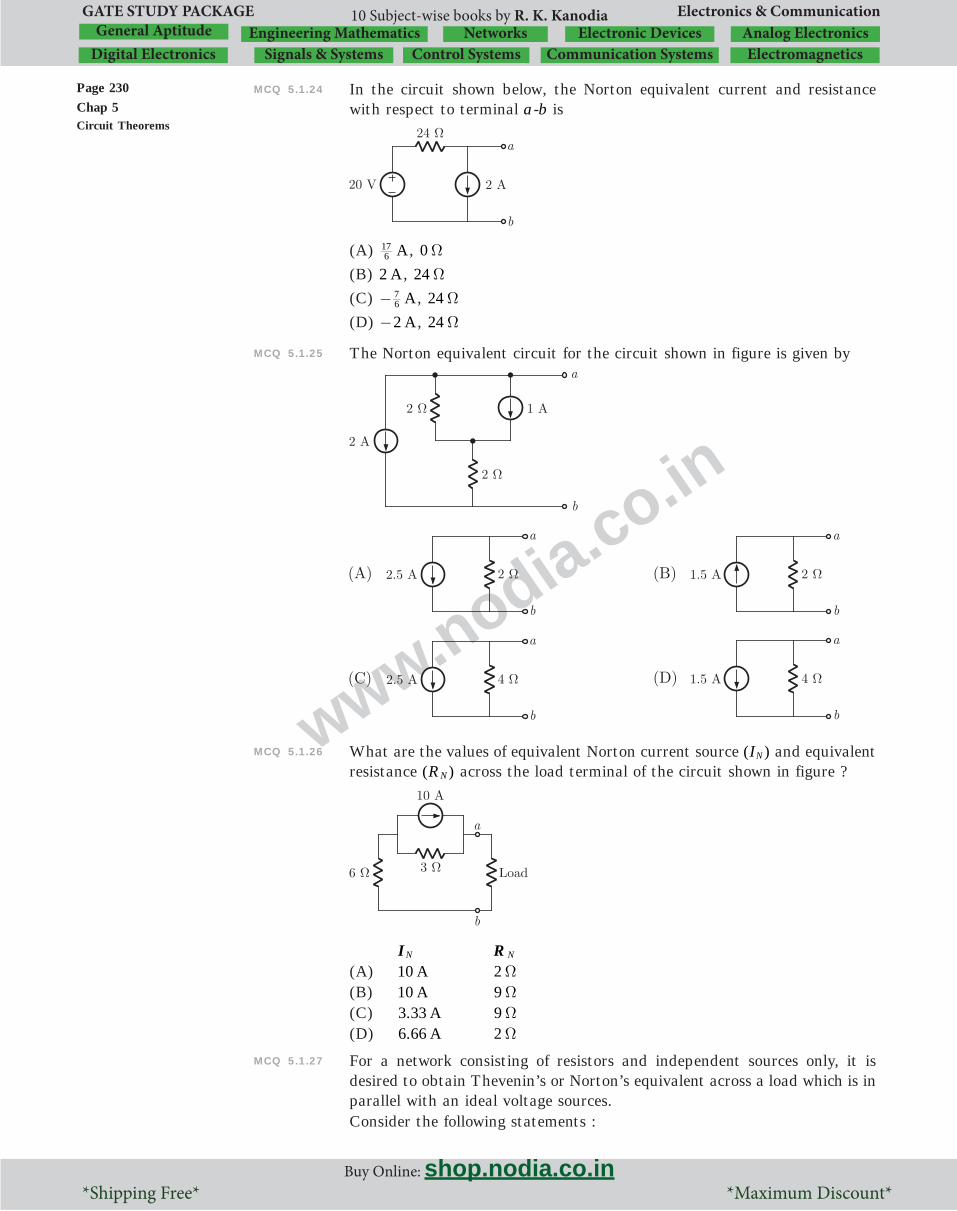
Page 230Chap 5Circuit Theorems
www.nodia.co.in
GATE STUDY PACKAGE Electronics & Communication
Buy Online: shop.nodia.co.in *Shipping Free* *Maximum Discount*
10 Subject-wise books by R. K. KanodiaNetworks Electronic Devices Analog Electronics
Digital Electronics Signals & Systems Control Systems ElectromagneticsCommunication SystemsGeneral Aptitude Engineering Mathematics
MCQ 5.1.24 In the circuit shown below, the Norton equivalent current and resistance with respect to terminal a -b is
(A) A617 , 0 W
(B) 2 A, 24 W(C) A6
7- , 24 W(D) 2 A- , 24 W
MCQ 5.1.25 The Norton equivalent circuit for the circuit shown in figure is given by
MCQ 5.1.26 What are the values of equivalent Norton current source ( )IN and equivalent resistance ( )RN across the load terminal of the circuit shown in figure ?
IN RN
(A) 10 A 2 W(B) 10 A 9 W(C) 3.33 A 9 W(D) 6.66 A 2 W
MCQ 5.1.27 For a network consisting of resistors and independent sources only, it is desired to obtain Thevenin’s or Norton’s equivalent across a load which is in parallel with an ideal voltage sources.Consider the following statements :

Page 231Chap 5
Circuit Theorems
www.nodia.co.in
Buy Online: shop.nodia.co.in *Shipping Free* *Maximum Discount*
GATE STUDY PACKAGE Electronics & Communication
Sample Chapter of Network Analysis (Vol-3, GATE Study Package)
1. Thevenin equivalent circuit across this terminal does not exist.
2. The Thevenin equivalent circuit exists and it is simply that of a voltage source.
3. The Norton equivalent circuit for this terminal does not exist.
Which of the above statements is/are true ?(A) 1 and 3 (B) 1 only
(C) 2 and 3 (D) 3 only
MCQ 5.1.28 For a network consisting of resistors and independent sources only, it is desired to obtain Thevenin’s or Norton’s equivalent across a load which is in series with an ideal current sources.Consider the following statements1. Norton equivalent across this terminal is not feasible.
2. Norton equivalent circuit exists and it is simply that of a current source only.
3. Thevenin’s equivalent circuit across this terminal is not feasible.
Which of the above statements is/are correct ?(A) 1 and 3
(B) 2 and 3
(C) 1 only
(D) 3 only
MCQ 5.1.29 The Norton equivalent circuit of the given network with respect to the terminal a -b , is
MCQ 5.1.30 In the circuit below, if RL is fixed and Rs is variable then for what value of Rs power dissipated in RL will be maximum ?
(A) R RS L= (B) R 0S =(C) /R R 2S L= (D) R R2S L=

Page 232Chap 5Circuit Theorems
www.nodia.co.in
GATE STUDY PACKAGE Electronics & Communication
Buy Online: shop.nodia.co.in *Shipping Free* *Maximum Discount*
10 Subject-wise books by R. K. KanodiaNetworks Electronic Devices Analog Electronics
Digital Electronics Signals & Systems Control Systems ElectromagneticsCommunication SystemsGeneral Aptitude Engineering Mathematics
MCQ 5.1.31 In the circuit shown below the maximum power transferred to RL is Pmax, then
(A) 12RL W= , 12 WPmax =(B) 3RL W= , 96 WPmax =(C) 3RL W= , 48 WPmax =(D) 12RL W= , 24 WPmax =
MCQ 5.1.32 In the circuit shown in figure (A) if current 2 AI1 = , then current I2 and I3 in figure (B) and figure (C) respectively are
(A) 2 A, 2 A
(B) 2 A- , 2 A
(C) 2 A, 2 A-
(D) 2 A- , 2 A-
MCQ 5.1.33 In the circuit of figure (A), if 20 mAI1 = , then what is the value of current I2 in the circuit of figure (B) ?
(A) 40 mA
(B) 20 mA-(C) 20 mA
(D) R1, R2 and R3 must be known

Page 233Chap 5
Circuit Theorems
www.nodia.co.in
Buy Online: shop.nodia.co.in *Shipping Free* *Maximum Discount*
GATE STUDY PACKAGE Electronics & Communication
Sample Chapter of Network Analysis (Vol-3, GATE Study Package)
MCQ 5.1.34 If 2 VV1 = in the circuit of figure (A), then what is the value of V2 in the circuit of figure (B) ?
(A) 2 V (B) 2 V-(C) 4 V (D) R1, R2 and R3 must be known
MCQ 5.1.35 The value of current I in the circuit below is equal to
(A)100 mA (B) 10 mA
(C) 233.34 mA (D) none of these
MCQ 5.1.36 A simple equivalent circuit of the two-terminal network shown in figure is
MCQ 5.1.37 If V AV BV CI1 2 3= + + in the following circuit, then values of A, B and C respectively are
(A) , ,32
32
31 (B) , ,3
131
3100
(C) , ,21
21
31 (D) , ,3
132
3100

Page 234Chap 5Circuit Theorems
www.nodia.co.in
GATE STUDY PACKAGE Electronics & Communication
Buy Online: shop.nodia.co.in *Shipping Free* *Maximum Discount*
10 Subject-wise books by R. K. KanodiaNetworks Electronic Devices Analog Electronics
Digital Electronics Signals & Systems Control Systems ElectromagneticsCommunication SystemsGeneral Aptitude Engineering Mathematics
MCQ 5.1.38 For the linear network shown below, V -I characteristic is also given in the figure. The value of Norton equivalent current and resistance respectively are
(A) 3 A, 2 W (B) 6 W, 2 W(C) 6 A, 0.5 W (D) 3 A, 0.5 W
MCQ 5.1.39 In the following circuit a network and its Thevenin and Norton equivalent are given.
The value of the parameter are
VTh RTh IN RN
(A) 4 V 2 W 2 A 2 W
(B) 4 V 2 W 2 A 3 W
(C) 8 V 1.2 W 330 A 1.2 W
(D) 8 V 5 W 58 A 5 W
MCQ 5.1.40 For the following circuit the value of equivalent Norton current IN and resistance RN are
(A) 2 A, 20 W (B) 2 A, 20- W(C) 0 A, 20 W (D) 0 A, 20- W
MCQ 5.1.41 Consider the following circuits shown below

Page 235Chap 5
Circuit Theorems
www.nodia.co.in
Buy Online: shop.nodia.co.in *Shipping Free* *Maximum Discount*
GATE STUDY PACKAGE Electronics & Communication
Sample Chapter of Network Analysis (Vol-3, GATE Study Package)
The relation between Ia and Ib is(A) 6I Ib a= +
(B) 2I Ib a= +(C) 1.5I Ib a=
(D) I Ib a=
Common Data For Q. 42 and 43 :In the following circuit, some measurements were made at the terminals a , b and given in the table below.
MCQ 5.1.42 The Thevenin equivalent of the unknown network across terminal a -b is(A) 3 W, 14 V (B) 5 W, 16 V
(C) 16 W, 38 V (D) 10 W, 26 V
MCQ 5.1.43 The value of R that will cause I to be 1 A, is(A) 22 W (B) 16 W(C) 8 W (D) 11 W
MCQ 5.1.44 In the circuit shown in fig (A) if current . AI 2 51 = then current I2 and I3 in fig (B) and (C) respectively are
(A) 5 A, 10 A (B) 5 A- , 10 A
(C) 5 A, 10 A- (D) 5 A- , 10 A-
MCQ 5.1.45 The V -I relation of the unknown element X in the given network is V AI B= + . The value of A (in ohm) and B (in volt) respectively are

Page 236Chap 5Circuit Theorems
www.nodia.co.in
GATE STUDY PACKAGE Electronics & Communication
Buy Online: shop.nodia.co.in *Shipping Free* *Maximum Discount*
10 Subject-wise books by R. K. KanodiaNetworks Electronic Devices Analog Electronics
Digital Electronics Signals & Systems Control Systems ElectromagneticsCommunication SystemsGeneral Aptitude Engineering Mathematics
(A) ,2 20 (B) ,2 8
(C) 0.5, 4 (D) . ,0 5 16
MCQ 5.1.46 For the following network the V -I curve with respect to terminals a -b , is given by
MCQ 5.1.47 A network N feeds a resistance R as shown in circuit below. Let the power consumed by R be P . If an identical network is added as shown in figure, the power consumed by R will be
(A) equal to P (B) less than P
(C) between P and 4P (D) more than 4P

Page 237Chap 5
Circuit Theorems
www.nodia.co.in
Buy Online: shop.nodia.co.in *Shipping Free* *Maximum Discount*
GATE STUDY PACKAGE Electronics & Communication
Sample Chapter of Network Analysis (Vol-3, GATE Study Package)
MCQ 5.1.48 A certain network consists of a large number of ideal linear resistors, one of which is R and two constant ideal source. The power consumed by R is P1 when only the first source is active, and P2 when only the second source is active. If both sources are active simultaneously, then the power consumed by R is(A) P P1 2! (B) P P1 2!
(C) ( )P P1 22! (D) ( )P P1 2
2!
MCQ 5.1.49 If the 60 W resistance in the circuit of figure (A) is to be replaced with a current source Is and 240 W shunt resistor as shown in figure (B), then magnitude and direction of required current source would be
(A) 200 mA, upward
(B) 150 mA, downward
(C) 50 mA, downward
(D) 150 mA, upward
MCQ 5.1.50 The Thevenin’s equivalent of the circuit shown in the figure is
(A) 4 V, 48 W
(B) 24 V, 12 W(C) 24 V, 24 W
(D) 12 V, 12 W
MCQ 5.1.51 The voltage VL across the load resistance in the figure is given by
VL V R RR
L
L= +b l
V and R will be equal to
(A) 10 V- , 2 W (B) 10 V, 2 W(C) 10 V- , 2 W- (D) none of these

Page 238Chap 5Circuit Theorems
www.nodia.co.in
GATE STUDY PACKAGE Electronics & Communication
Buy Online: shop.nodia.co.in *Shipping Free* *Maximum Discount*
10 Subject-wise books by R. K. KanodiaNetworks Electronic Devices Analog Electronics
Digital Electronics Signals & Systems Control Systems ElectromagneticsCommunication SystemsGeneral Aptitude Engineering Mathematics
MCQ 5.1.52 In the circuit given below, viewed from a -b , the circuit can be reduced to an equivalent circuit as
(A) 10 volt source in series with 2 kW resistor
(B) 1250 W resistor only
(C) 20 V source in series with 1333.34 W resistor
(D) 800 W resistor only
MCQ 5.1.53 The V -I equation for the network shown in figure, is given by
(A) 7 200 54V I= + (B) V I100 36= +(C) V I200 54= + (D) V I50 54= +
MCQ 5.1.54 In the following circuit the value of open circuit voltage and Thevenin resistance at terminals ,a b are
(A) 100 VVoc = , 1800RTh W=
(B) 0 VVoc = , 270RTh W=(C) 100 VVoc = , 90RTh W=
(D) 0 VVoc = , 90RTh W=
***********

Page 239Chap 5
Circuit Theorems
www.nodia.co.in
Buy Online: shop.nodia.co.in *Shipping Free* *Maximum Discount*
GATE STUDY PACKAGE Electronics & Communication
Sample Chapter of Network Analysis (Vol-3, GATE Study Package)
EXERCISE 5.2
QUES 5.2.1 In the given network, if V Vs 0= , 1 AI = . If V V2s 0= then what is the value of I1 (in Amp) ?
QUES 5.2.2 In the given network, if I Is 0= then 1 voltV = . What is the value of I1 (in Amp) if I I2s 0= ?
QUES 5.2.3 In the circuit below, the voltage V across the 04 W resistor would be equal to ____ Volts.
QUES 5.2.4 The value of current I flowing through 2 W resistance in the given circuit, equals to ____ Amp.
QUES 5.2.5 In the given circuit, the value of current I will be _____Amps.
QUES 5.2.6 What is the value of current I in the given network (in Amp) ?

Page 240Chap 5Circuit Theorems
www.nodia.co.in
GATE STUDY PACKAGE Electronics & Communication
Buy Online: shop.nodia.co.in *Shipping Free* *Maximum Discount*
10 Subject-wise books by R. K. KanodiaNetworks Electronic Devices Analog Electronics
Digital Electronics Signals & Systems Control Systems ElectromagneticsCommunication SystemsGeneral Aptitude Engineering Mathematics
QUES 5.2.7 In the given network if V V 021 = = , then what is the value of Vo (in volts) ?
QUES 5.2.8 What is the value of current I in the circuit shown below (in Amp) ?
QUES 5.2.9 How much power is being dissipated by the 4 kW resistor in the network (in mW) ?
QUES 5.2.10 Thevenin equivalent resistance RTh between the nodes a and b in the following circuit is ____ W .
Common Data For Q. 11 and 12 :
Consider the circuit shown in the figure.
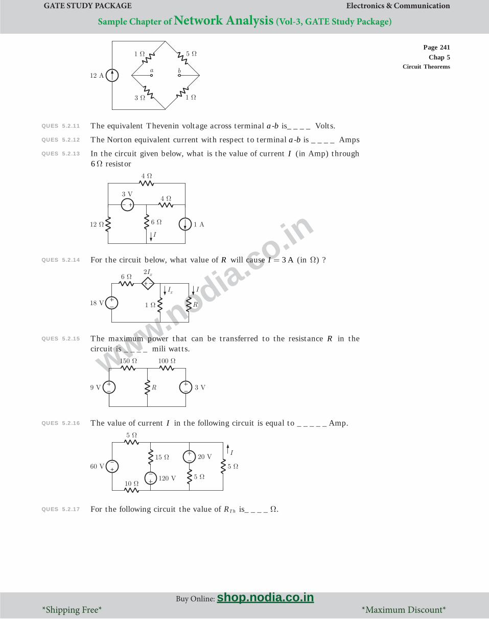
Page 241Chap 5
Circuit Theorems
www.nodia.co.in
Buy Online: shop.nodia.co.in *Shipping Free* *Maximum Discount*
GATE STUDY PACKAGE Electronics & Communication
Sample Chapter of Network Analysis (Vol-3, GATE Study Package)
QUES 5.2.11 The equivalent Thevenin voltage across terminal a -b is____ Volts.
QUES 5.2.12 The Norton equivalent current with respect to terminal a -b is ____ Amps
QUES 5.2.13 In the circuit given below, what is the value of current I (in Amp) through 6 W resistor
QUES 5.2.14 For the circuit below, what value of R will cause AI 3= (in W ) ?
QUES 5.2.15 The maximum power that can be transferred to the resistance R in the circuit is ____ mili watts.
QUES 5.2.16 The value of current I in the following circuit is equal to _____Amp.
QUES 5.2.17 For the following circuit the value of RTh is____W .

Page 242Chap 5Circuit Theorems
www.nodia.co.in
GATE STUDY PACKAGE Electronics & Communication
Buy Online: shop.nodia.co.in *Shipping Free* *Maximum Discount*
10 Subject-wise books by R. K. KanodiaNetworks Electronic Devices Analog Electronics
Digital Electronics Signals & Systems Control Systems ElectromagneticsCommunication SystemsGeneral Aptitude Engineering Mathematics
QUES 5.2.18 What is the value of current I in the given network (in Amp) ?
QUES 5.2.19 The value of current I in the figure is _____ mA.
QUES 5.2.20 For the circuit of figure, some measurements were made at the terminals a -b and given in the table below.
What is the value of IL (in Amps) for 20RL W= ?
QUES 5.2.21 In the circuit below, for what value of k , load 2RL W= absorbs maximum power ?
QUES 5.2.22 In the circuit shown below, the maximum power that can be delivered to the load RL is equal to _____ mW.
QUES 5.2.23 A practical DC current source provide 20 kW to a 50 W load and 20 kW to a 200 W load. The maximum power, that can drawn from it, is ____ kW.

Page 243Chap 5
Circuit Theorems
www.nodia.co.in
Buy Online: shop.nodia.co.in *Shipping Free* *Maximum Discount*
GATE STUDY PACKAGE Electronics & Communication
Sample Chapter of Network Analysis (Vol-3, GATE Study Package)
QUES 5.2.24 In the following circuit the value of voltage V1 is ____ Volts.
QUES 5.2.25 If 5 AI = in the circuit below, then what is the value of voltage source Vs (in volts)?
QUES 5.2.26 For the following circuit, what is the value of current I (in Amp) ?
QUES 5.2.27 The Thevenin equivalent resistance between terminal a and b in the following circuit is _____ W .
QUES 5.2.28 In the circuit shown below, what is the value of current I (in Amps) ?
QUES 5.2.29 The power delivered by 12 V source in the given network is ____ watts.

Page 244Chap 5Circuit Theorems
www.nodia.co.in
GATE STUDY PACKAGE Electronics & Communication
Buy Online: shop.nodia.co.in *Shipping Free* *Maximum Discount*
10 Subject-wise books by R. K. KanodiaNetworks Electronic Devices Analog Electronics
Digital Electronics Signals & Systems Control Systems ElectromagneticsCommunication SystemsGeneral Aptitude Engineering Mathematics
QUES 5.2.30 In the circuit shown, what value of RL (in W ) maximizes the power delivered to RL ?
QUES 5.2.31 The V -I relation for the circuit below is plotted in the figure. The maximum power that can be transferred to the load RL will be ______ mW
QUES 5.2.32 In the following circuit equivalent Thevenin resistance between nodes a and b is 3RTh W= . The value of a is_____
QUES 5.2.33 The maximum power that can be transferred to the load resistor RL from the current source in the figure is ____ watts.
Common Data For Q. 34 and 35
An electric circuit is fed by two independent sources as shown in figure.
QUES 5.2.34 The power supplied by 36 V source will be _____ watts.
QUES 5.2.35 The power supplied by 27 A source will be _____ watts.

Page 245Chap 5
Circuit Theorems
www.nodia.co.in
Buy Online: shop.nodia.co.in *Shipping Free* *Maximum Discount*
GATE STUDY PACKAGE Electronics & Communication
Sample Chapter of Network Analysis (Vol-3, GATE Study Package)
QUES 5.2.36 In the circuit shown in the figure, what is the power dissipated in 4 W resistor (in watts)
QUES 5.2.37 What is the value of voltage V in the following network (in volts) ?
QUES 5.2.38 For the circuit shown in figure below the value of RTh is ____W .
QUES 5.2.39 Consider the network shown below :
The power absorbed by load resistance RL is shown in table :
RL 10 kW 30 kW
P 3.6 mW 4.8 mW
The value of RL (in kW ), that would absorb maximum power, is____
***********

Page 246Chap 5Circuit Theorems
www.nodia.co.in
GATE STUDY PACKAGE Electronics & Communication
Buy Online: shop.nodia.co.in *Shipping Free* *Maximum Discount*
10 Subject-wise books by R. K. KanodiaNetworks Electronic Devices Analog Electronics
Digital Electronics Signals & Systems Control Systems ElectromagneticsCommunication SystemsGeneral Aptitude Engineering Mathematics
SOLUTIONS 5.1
SOL 5.1.1 Option (B) is correct.
For, Vs 10 V= , 40 WP =
So, Is 4 AVP
1040
s= = =
Now, Vsl 5 V= , so 2 AIs =l (From linearity)
New value of the power supplied by source is
Psl 5 2 10 WV Is s #= = =l l
Note: Linearity does not apply to power calculations.
SOL 5.1.2 Option (C) is correct.
From linearity, we know that in the circuit IV
L
s ratio remains constant
IV
L
s 200 10
20 1003#
= =-
Let current through load is ILl when the power absorbed is 2.5 W, so
PL ( )I RL L2= l
2.5 ( )I 10L2#= l
ILl 0.5 A=
IV
L
s IV 100
L
s= =ll
So, Vsl 100 100 0.5 50 VIL #= = =l
Thus required values are
ILl 0.5 A= , 50 VVs =l
SOL 5.1.3 Option (D ) is correct.From linearity,
IL AV BIs s= + , A and B are constants
From the table 2 A B14 6= + ...(1)
6 A B18 2= + ...(2)Solving equation (1) & (2)
.A 0 4= , .B 0 6=-
So, IL . .V I0 4 0 6s s= -
SOL 5.1.4 Option (B) is correct.The circuit has 3 independent sources, so we apply superposition theorem to obtain the voltage drop.Due to 16 V source only : (Open circuit 5 A source and Short circuit 32 V source)

Page 247Chap 5
Circuit Theorems
www.nodia.co.in
Buy Online: shop.nodia.co.in *Shipping Free* *Maximum Discount*
GATE STUDY PACKAGE Electronics & Communication
Sample Chapter of Network Analysis (Vol-3, GATE Study Package)
Let voltage across R2 due to 16 V source only is V1.
Using voltage division
V1 ( )24 88 16=- +
4 V=-Due to 5 A source only : (Short circuit both the 16 V and 32 V sources)
Let voltage across R2 due to 5 A source only is V2.
V2 ( || 16 || 16 ) 524 #W W W= 6 5 30 volt#= =Due to 32 V source only : (Short circuit 16 V source and open circuit 5 A source)Let voltage across R2 due to V32 source only is V3
Using voltage division
V3 .. (32) 12 V16 9 6
9 6= + =
By superposition, the net voltage across R2 is
V V V V1 2 3= + + 4 30 12=- + + 38 volt=
ALTERNATIVE METHOD :
The problem may be solved by applying a node equation at the top node.
SOL 5.1.5 Option (C) is correctDue to 60 A Source Only : (Open circuit 30 A and short circuit 30 V sources)
12 || 6W W 4 W=

Page 248Chap 5Circuit Theorems
www.nodia.co.in
GATE STUDY PACKAGE Electronics & Communication
Buy Online: shop.nodia.co.in *Shipping Free* *Maximum Discount*
10 Subject-wise books by R. K. KanodiaNetworks Electronic Devices Analog Electronics
Digital Electronics Signals & Systems Control Systems ElectromagneticsCommunication SystemsGeneral Aptitude Engineering Mathematics
Using current division
Ia (60) 12 A2 82= + =
Again, Ia will be distributed between parallel combination of 12 W and 6 W
I1 (12) 4 A12 66= + =
Due to 30 A source only : (Open circuit 60 A and short circuit 30 V sources)
Using current division
Ib 4 (30) 12 A4 6= + =
Ib will be distributed between parallel combination of 12 W and 6 W
I2 (12) 4 A12 66= + =
Due to 30 V Source Only : (Open circuit 60 A and 30 A sources)
Using source transformation
Using current division
I3 (5) 1 A12 33=- + =-
SOL 5.1.6 Option (C) is correct.
Using superposition, I I I1 2= +Let I1 is the current due to 9 A source only. (i.e. short 18 V source)
I1 (9) 3 A6 126= + = (current division)
Let I2 is the current due to 18 V source only (i.e. open 9 A source)
I2 1 A6 1218= + =

Page 249Chap 5
Circuit Theorems
www.nodia.co.in
Buy Online: shop.nodia.co.in *Shipping Free* *Maximum Discount*
GATE STUDY PACKAGE Electronics & Communication
Sample Chapter of Network Analysis (Vol-3, GATE Study Package)
So, 3 AI1 = , 1 AI2 =
SOL 5.1.7 Option (B) is correct.From superposition theorem, it is known that if all source values are doubled, then node voltages also be doubled.
SOL 5.1.8 Option (A) is correct.From the principal of superposition, doubling the values of voltage source doubles the mesh currents.
SOL 5.1.9 Option (C) is correct.Using source transformation, we can obtain I in following steps.
I 2 A3 46 8
714= +
+ = =
ALTERNATIVE METHOD :Try to solve the problem by obtaining Thevenin equivalent for right half of the circuit.
SOL 5.1.10 Option (D) is correct.Using source transformation of 4 A and 6 V source.
Adding parallel current sources

Page 250Chap 5Circuit Theorems
www.nodia.co.in
GATE STUDY PACKAGE Electronics & Communication
Buy Online: shop.nodia.co.in *Shipping Free* *Maximum Discount*
10 Subject-wise books by R. K. KanodiaNetworks Electronic Devices Analog Electronics
Digital Electronics Signals & Systems Control Systems ElectromagneticsCommunication SystemsGeneral Aptitude Engineering Mathematics
Source transformation of 5 A source
Applying KVL around the anticlockwise direction
I I5 8 2 12- - + - - 0= I9 3- - 0= I 3 A=-Power absorbed by 12 V source
P12 V I12#= (Passive sign convention)
12 3#= - 36 W=-or, 12 V source supplies 36 W power.
SOL 5.1.11 Option (B) is correct.We know that source transformation also exists for dependent source, so
Current source values
Is I I2
6 3xx= = (downward)
Rs 2 W=
SOL 5.1.12 Option (C) is correct.We know that source transformation is applicable to dependent source also.Values of equivalent voltage source
Vs ( )( )I I4 5 20x x= = Rs 5 W=
SOL 5.1.13 Option (C) is correct.Combining the parallel resistance and adding the parallel connected current sources.
9 3A A- 6 A= (upward)
3 || 6W W 2 W=

Page 251Chap 5
Circuit Theorems
www.nodia.co.in
Buy Online: shop.nodia.co.in *Shipping Free* *Maximum Discount*
GATE STUDY PACKAGE Electronics & Communication
Sample Chapter of Network Analysis (Vol-3, GATE Study Package)
Source transformation of 6 A source
SOL 5.1.14 Option (D) is correct.Thevenin Voltage : (Open Circuit Voltage)The open circuit voltage between a -b can be obtained as
Writing KCL at node a
1V24
10Th - + 0=
10 24VTh - + 0= or VTh 14 volt=-Thevenin Resistance :To obtain Thevenin’s resistance, we set all independent sources to zero i.e., short circuit all the voltage sources and open circuit all the current sources.
RTh 24 W=
SOL 5.1.15 Option (B) is correct.Thevenin Voltage :
Using voltage division V1 (10) 4 volt20 3020= + =
and, V2 (10) 6 volt15 1015= + =
Applying KVL, V V Vab1 2- + 0= 4 6 Vab- + 0=

Page 252Chap 5Circuit Theorems
www.nodia.co.in
GATE STUDY PACKAGE Electronics & Communication
Buy Online: shop.nodia.co.in *Shipping Free* *Maximum Discount*
10 Subject-wise books by R. K. KanodiaNetworks Electronic Devices Analog Electronics
Digital Electronics Signals & Systems Control Systems ElectromagneticsCommunication SystemsGeneral Aptitude Engineering Mathematics
VTh 2 voltVab= =-
Thevenin Resistance :
Rab [20 || ] [15 || 10 ]30W W W W= + 12 6 18W W W= + = RTh 18Rab W= =
SOL 5.1.16 Option (A) is a correct.Using source transformation of 24 V source
Adding parallel connected sources
So, VTh 4 V= , 6RTh W=
SOL 5.1.17 Option (A) is correct.Thevenin Voltage: (Open Circuit Voltage)

Page 253Chap 5
Circuit Theorems
www.nodia.co.in
Buy Online: shop.nodia.co.in *Shipping Free* *Maximum Discount*
GATE STUDY PACKAGE Electronics & Communication
Sample Chapter of Network Analysis (Vol-3, GATE Study Package)
VTh ( )6 46 40= + - 24 volt=- (using voltage division)
Thevenin Resistance :
RTh 6 || 4 2.46 46 4#W W W= = + =
SOL 5.1.18 Option (B) is correct.For the circuit of figure (A)
VTh V Va b= - Va 24 V=
Vb ( 6) 4 V6 36= + - =- (Voltage division)
VTh 24 ( 4) 28 V= - - =For the circuit of figure (B), using source transformation
Combining parallel resistances,
12 || 4W W 3 W=Adding parallel current sources,
8 4- 4 A= (downward)
VTh 12 V=-
SOL 5.1.19 Option (C) is correct.For the circuit for fig (A)

Page 254Chap 5Circuit Theorems
www.nodia.co.in
GATE STUDY PACKAGE Electronics & Communication
Buy Online: shop.nodia.co.in *Shipping Free* *Maximum Discount*
10 Subject-wise books by R. K. KanodiaNetworks Electronic Devices Analog Electronics
Digital Electronics Signals & Systems Control Systems ElectromagneticsCommunication SystemsGeneral Aptitude Engineering Mathematics
RTh 6 || 3 2Rab W W W= = =For the circuit of fig (B), as obtained in previous solution.
RTh 3 W=
SOL 5.1.20 Option (B) is correct.
The current source connected in parallel with load does not affect Thevenin equivalent circuit. Thus, Thevenin equivalent circuit will contain its usual form of a voltage source in series with a resistor.
SOL 5.1.21 Option (C) is correct.The network consists of resistor and dependent sources because if it has independent source then there will be an open circuit Thevenin voltage present.
SOL 5.1.22 Option (D) is correct.Thevenin Voltage (Open Circuit Voltage) :
Applying KCL at top middle node
1V V V3
26
Th x Th- + + 0=
V V V32
6 1Th Th Th- + + 0= ( )V VTh x=
V V2 6Th Th- + + 0= VTh 6 volt=Thevenin Resistance :
RTh Short circuit currentOpen circuit voltage
IV
sc
Th= =
To obtain Thevenin resistance, first we find short circuit current through a -b

Page 255Chap 5
Circuit Theorems
www.nodia.co.in
Buy Online: shop.nodia.co.in *Shipping Free* *Maximum Discount*
GATE STUDY PACKAGE Electronics & Communication
Sample Chapter of Network Analysis (Vol-3, GATE Study Package)
Writing KCL at top middle node
V V V V32
6 1 30x x x x- + + + - 0=
V V V2 6 2x x x- + + + 0= or Vx 6 volt=-
Isc 2 AV3
036x= - =- =-
Thevenin’s resistance, RTh 3IV
26
sc
Th W= =- =-
ALTERNATIVE METHOD :Since dependent source is present in the circuit, we put a test source across a -b to obtain Thevenin’s equivalent.
By applying KCL at top middle node
V V V V V32
6 1 3x x x x test- + + + - 0=
V V V V2 6 2 2x x x test- + + + - 0= V V2 test x- 6= ...(1)
We have Itest V V
3test x= -
I3 test V Vtest x= - Vx V I3test test= -Put Vx into equation (1)
( )V V I2 3test test test- - 6= V V I2 3test test test- + 6= Vtest I6 3 test= - ...(2)For Thevenin’s equivalent circuit
RV V
Th
test Th- Itest=
Vtest V R ITh Th test= + ...(3)Comparing equation (2) and (3)
VTh 6 V= , 3RTh W=-

Page 256Chap 5Circuit Theorems
www.nodia.co.in
GATE STUDY PACKAGE Electronics & Communication
Buy Online: shop.nodia.co.in *Shipping Free* *Maximum Discount*
10 Subject-wise books by R. K. KanodiaNetworks Electronic Devices Analog Electronics
Digital Electronics Signals & Systems Control Systems ElectromagneticsCommunication SystemsGeneral Aptitude Engineering Mathematics
SOL 5.1.23 Option (D) is correct.
Using voltage division
V V R RR
ThTh
= +b l
From the table,
6 V R33
ThTh
= +b l ...(1)
8 V R88
ThTh
= +b l ...(2)
Dividing equation (1) and (2), we get
86
( )( )
RR
8 33 8
Th
Th= ++
R6 2 Th+ R8 Th= + RTh 2 W=Substituting RTh into equation (1)
6 V 3 23
Th= +b l or VTh 10 V=
SOL 5.1.24 Option (C) is correct.Norton Current : (Short Circuit Current)The Norton equivalent current is equal to the short-circuit current that would flow when the load replaced by a short circuit as shown below
Applying KCL at node a
I I 2N 1+ + 0=
Since I1 A240 20
65= - =-
So, I 65 2N - + 0=
IN A67=-
Norton Resistance :Set all independent sources to zero (i.e. open circuit current sources and short circuit voltage sources) to obtain Norton’s equivalent resistance RN .
RN 24 W=

Page 257Chap 5
Circuit Theorems
www.nodia.co.in
Buy Online: shop.nodia.co.in *Shipping Free* *Maximum Discount*
GATE STUDY PACKAGE Electronics & Communication
Sample Chapter of Network Analysis (Vol-3, GATE Study Package)
SOL 5.1.25 Option (C) is correct.Using source transformation of 1 A source
Again, source transformation of 2 V source
Adding parallel current sources
ALTERNATIVE METHOD :Try to solve the problem using superposition method.
SOL 5.1.26 Option (C) is correct.Short circuit current across terminal a -b is
For simplicity circuit can be redrawn as
IN ( )3 63 10= + (Current division)
3.33 A=Norton’s equivalent resistance
RN 6 3 9 W= + =

Page 258Chap 5Circuit Theorems
www.nodia.co.in
GATE STUDY PACKAGE Electronics & Communication
Buy Online: shop.nodia.co.in *Shipping Free* *Maximum Discount*
10 Subject-wise books by R. K. KanodiaNetworks Electronic Devices Analog Electronics
Digital Electronics Signals & Systems Control Systems ElectromagneticsCommunication SystemsGeneral Aptitude Engineering Mathematics
SOL 5.1.27 Option (C) is correct.
The voltage across load terminal is simply Vs and it is independent of any other current or voltage. So, Thevenin equivalent is V VTh s= and R 0Th = (Voltage source is ideal). Norton equivalent does not exist because of parallel connected voltage source.
SOL 5.1.28 Option (B) is correct.
The output current from the network is equal to the series connected current source only, so I IN s= . Thus, effect of all other component in the network does not change IN .In this case Thevenin’s equivalent is not feasible because of the series connected current source.
SOL 5.1.29 Option (C) is correct.Norton Current : (Short Circuit Current)
Using source transformation
Nodal equation at top center node
( )
I60 24
3 30 6
N- + +
- - + 0=
4 1 IN- + + 0= IN 3 A=Norton Resistance :

Page 259Chap 5
Circuit Theorems
www.nodia.co.in
Buy Online: shop.nodia.co.in *Shipping Free* *Maximum Discount*
GATE STUDY PACKAGE Electronics & Communication
Sample Chapter of Network Analysis (Vol-3, GATE Study Package)
RN 6 || (3 3) 6 || 6 3Rab W= = + = =So, Norton equivalent will be
SOL 5.1.30 Option (B) is correct.
V V R RR
ss L
L= +b l
Power absorbed by RL
PL ( )
( )RV
R RV R
L s L
s L2
2
2
= =+
From above expression, it is known that power is maximum when 0Rs =
NOTE :Do not get confused with maximum power transfer theorem. According to maximum power transfer theorem if RL is variable and Rs is fixed then power dissipated by RL is maximum when R RL s= .
SOL 5.1.31 Option (C) is correct.We solve this problem using maximum power transfer theorem. First, obtain Thevenin equivalent across RL .Thevenin Voltage : (Open circuit voltage)
Using source transformation
Using nodal analysis V V6
242 4
24Th Th- + +- 0=
2V 48Th - 0 24 VVTh&= =
Thevenin Resistance :

Page 260Chap 5Circuit Theorems
www.nodia.co.in
GATE STUDY PACKAGE Electronics & Communication
Buy Online: shop.nodia.co.in *Shipping Free* *Maximum Discount*
10 Subject-wise books by R. K. KanodiaNetworks Electronic Devices Analog Electronics
Digital Electronics Signals & Systems Control Systems ElectromagneticsCommunication SystemsGeneral Aptitude Engineering Mathematics
RTh 6 || 6 3W W W= =Circuit becomes as
For maximum power transfer
RL 3RTh W= =Value of maximum power
Pmax ( )
RV4 L
Th2
= 4 3( )
48 W24 2
#= =
SOL 5.1.32 Option (D) is correct.This can be solved by reciprocity theorem. But we have to take care that the polarity of voltage source have the same correspondence with branch current in each of the circuit.In figure (B) and figure (C), polarity of voltage source is reversed with respect to direction of branch current so
IV
1
1 IV
IV
2
2
3
3=- =-
I2 2 AI3= =-
SOL 5.1.33 Option (C) is correct.According to reciprocity theorem in any linear bilateral network when a single voltage source Va in branch a produces a current Ib in branches b, then if the voltage source Va is removed(i.e. branch a is short circuited) and inserted in branch b, then it will produce a current Ib in branch a.
So, I2 20 mAI1= =
SOL 5.1.34 Option (A) is correct.According to reciprocity theorem in any linear bilateral network when a single current source Ia in branch a produces a voltage Vb in branches b, then if the current source Ia is removed(i.e. branch a is open circuited) and inserted in branch b, then it will produce a voltage Vb in branch a.
So, V2 2 volt=
SOL 5.1.35 Option (A) is correct.We use Millman’s theorem to obtain equivalent resistance and voltage across a -b .
Vab 24096
20040
80080
2401
2001
8001=
+ +
- + + - 28.8 V5
144=- =-
The equivalent resistance
Rab 96
2401
2001
8001
1 W=+ +
=

Page 261Chap 5
Circuit Theorems
www.nodia.co.in
Buy Online: shop.nodia.co.in *Shipping Free* *Maximum Discount*
GATE STUDY PACKAGE Electronics & Communication
Sample Chapter of Network Analysis (Vol-3, GATE Study Package)
Now, the circuit is reduced as
I . 100 mA96 19228 8= + =
SOL 5.1.36 Option (B) is correct.Thevenin Voltage: (Open circuit voltage):The open circuit voltage will be equal to V , i.e. V VTh =Thevenin Resistance:Set all independent sources to zero i.e. open circuit the current source and short circuit the voltage source as shown in figure
Open circuit voltage V1=
SOL 5.1.37 Option (B) is correct.V is obtained using super position.Due to source V1 only : (Open circuit source I3 and short circuit source V2)
V ( )V100 5050
1= + V31
1= (using voltage division)
so, A 31=
Due to source V2 only : (Open circuit source I3 and short circuit source V1)
V ( )V100 5050
2= + V31
2= (Using voltage division)
So, B 31=
Due to source I3 only : (short circuit sources V1 and V2)

Page 262Chap 5Circuit Theorems
www.nodia.co.in
GATE STUDY PACKAGE Electronics & Communication
Buy Online: shop.nodia.co.in *Shipping Free* *Maximum Discount*
10 Subject-wise books by R. K. KanodiaNetworks Electronic Devices Analog Electronics
Digital Electronics Signals & Systems Control Systems ElectromagneticsCommunication SystemsGeneral Aptitude Engineering Mathematics
V [ || | | ]I 100 100 1003= I 3100
3= b l
So, C 3100=
ALTERNATIVE METHOD :
Try to solve by nodal method, taking a supernode corresponding to voltage
source V2.
SOL 5.1.38 Option (C) is correct.The circuit with Norton equivalent
So, I IN + RV
N=
I RV I
NN= - (General form)
From the given graph, the equation of line
I 2 6V= -Comparing with general form
R1N
2= or 0.5RN W=
IN 6 A=
SOL 5.1.39 Option (D) is correct.Thevenin voltage: (Open circuit voltage)
VTh 4 4 4 8 V2 2#= + = + =^ h
Thevenin Resistance:
RTh 2 3 5 RNW= + = =Norton Current:
IN ARV
58
Th
Th= =
SOL 5.1.40 Option (C) is correct.
Norton current, 0IN = because there is no independent source present in
the circuit.To obtain Norton resistance we put a 1 A test source across the load terminal as shown in figure.

Page 263Chap 5
Circuit Theorems
www.nodia.co.in
Buy Online: shop.nodia.co.in *Shipping Free* *Maximum Discount*
GATE STUDY PACKAGE Electronics & Communication
Sample Chapter of Network Analysis (Vol-3, GATE Study Package)
Norton or Thevenin resistance
RN V1test=
Writing KVL in the left mesh
I I I20 10 1 301 1 1+ - -^ h 0= I I I20 10 30 101 1 1- - + 0= I1 0.5 A=Writing KVL in the right mesh
V I5 1 30test 1- -^ h 0= 0.V 5 30 5test - - ^ h 0= V 5 15test - - 0=
RN 20V1test W= =
SOL 5.1.41 Option (C) is correct.In circuit (b) transforming the 3 A source in to 18 V source all source are 1.5 times of that in circuit (a) as shown in figure.
Using principal of linearity, 1.5I Ib a=
SOL 5.1.42 Option (B) is correct.
I R RV
Th
Th= +
From the table, 2 RV
3 Th
Th= + ...(1)
1.6 RV
5 Th
Th= + ...(2)
Dividing equation (1) and (2), we get
.1 62 R
R35
Th
Th= ++
R6 2 Th+ . R8 1 6 Th= + . R0 4 Th 2=

Page 264Chap 5Circuit Theorems
www.nodia.co.in
GATE STUDY PACKAGE Electronics & Communication
Buy Online: shop.nodia.co.in *Shipping Free* *Maximum Discount*
10 Subject-wise books by R. K. KanodiaNetworks Electronic Devices Analog Electronics
Digital Electronics Signals & Systems Control Systems ElectromagneticsCommunication SystemsGeneral Aptitude Engineering Mathematics
RTh 5 W=Substituting RTh into equation (1)
2 V3 5
Th= +
VTh 2(8) 16 V= =
SOL 5.1.43 Option (D) is correct.
We have, I R RV
Th
Th= +
16 VVTh = , 5RTh W=
I R516 1= + =
16 R5= + R 11 W=
SOL 5.1.44 Option (B) is correct.
It can be solved by reciprocity theorem. Polarity of voltage source should have same correspondence with branch current in each of the circuit. Polarity of voltage source and current direction are shown below
So, IV
1
1 IV
IV
2
2
3
3=- =
.2 510 I I
20 402 3
=- =
I2 5 A=- I3 10 A=
SOL 5.1.45 Option (A) is correct.To obtain V -I equation we find the Thevenin equivalent across the terminal at which X is connected.Thevenin Voltage : (Open Circuit Voltage)
V1 6 1 6 V#= = V V12 1 3+ - 0= (KVL in outer mesh)
V3 12 6 18 V= + = V V VTh 2 3- - 0= (KVL in Bottom right mesh)
VTh V V2 3= +
( 2 1 2 )VV2 #= = VTh 2 18 20 V= + =

Page 265Chap 5
Circuit Theorems
www.nodia.co.in
Buy Online: shop.nodia.co.in *Shipping Free* *Maximum Discount*
GATE STUDY PACKAGE Electronics & Communication
Sample Chapter of Network Analysis (Vol-3, GATE Study Package)
Thevenin Resistance :
RTh 1 1 2 W= + =Now, the circuit becomes as
I RV V
Th
Th= -
V R I VTh Th= +so A 2RTh W= = B 20 VVTh= =
ALTERNATIVE METHOD :
In the mesh ABCDEA, we have KVL equation as
( ) ( )V I I1 2 1 6 12- + - + - 0= V I2 20= +So, A 2= , B 2=
SOL 5.1.46 Option (A) is correct.To obtain V -I relation, we obtain either Norton equivalent or Thevenin equivalent across terminal a -b .Norton Current (short circuit current) :
Applying nodal analysis at center node
I 2N + 424= or IN 6 2 4 A= - =

Page 266Chap 5Circuit Theorems
www.nodia.co.in
GATE STUDY PACKAGE Electronics & Communication
Buy Online: shop.nodia.co.in *Shipping Free* *Maximum Discount*
10 Subject-wise books by R. K. KanodiaNetworks Electronic Devices Analog Electronics
Digital Electronics Signals & Systems Control Systems ElectromagneticsCommunication SystemsGeneral Aptitude Engineering Mathematics
Norton Resistance :
RN 4 W= (Both 2 W resistor are short circuited)Now, the circuit becomes as
IN RV I
N= +
4 V I4= +
16 V I4= +or V I4 16=- +
ALTERNATIVE METHOD : Solve by writing nodal equation at the center node.
SOL 5.1.47 Option (C) is correct.Let Thevenin equivalent of both networks are as shown below.
P R RV R
Th
Th2
= +b l (Single network N )
Pl R
V RRTh
2
2
Th=
+c m 4 R RV R2 Th
Th2
= +b l (Two N are added)
Thus 4P P P< <l
SOL 5.1.48 Option (C) is correct.
I1 RP1= and I R
P2
2=
Using superposition I I I1 2!= RP
RP1 2!=
I R2 ( )P P1 22!=

Page 267Chap 5
Circuit Theorems
www.nodia.co.in
Buy Online: shop.nodia.co.in *Shipping Free* *Maximum Discount*
GATE STUDY PACKAGE Electronics & Communication
Sample Chapter of Network Analysis (Vol-3, GATE Study Package)
SOL 5.1.49 Option (B) is correct.From the substitution theorem we know that any branch within a circuit can be replaced by an equivalent branch provided that replacement branch has the same current through it and voltage across it as the original branch.The voltage across the branch in the original circuit
V ( || )
||( )
40 60 1640 60
20= + 20 12 V4024
#= =
Current entering terminal a -b is
I 200 mARV
6012= = =
In fig(B), to maintain same voltage 12 VV = current through 240 W resistor must be
IR 50 mA24012= =
Using KCL at terminal a , as shown
I I IR S= + 200 I50 s= + Is 150 mA= , down wards
SOL 5.1.50 Option (B) is correct.Thevenin voltage : (Open Circuit Voltage)In the given problem, we use mesh analysis method to obtain Thevenin voltage
I3 0= (a -b is open circuit)
Writing mesh equations
Mesh 1: 36 12( ) 6( )I I I I1 2 1 3- - - - 0= 36 12 6I I I121 2 1- + - 0= ( )I 03 = I I3 2 21 - 6= ...(1)
Mesh 2: 24 20( ) 12( )I I I I I2 2 3 2 1- - - - - 0=

Page 268Chap 5Circuit Theorems
www.nodia.co.in
GATE STUDY PACKAGE Electronics & Communication
Buy Online: shop.nodia.co.in *Shipping Free* *Maximum Discount*
10 Subject-wise books by R. K. KanodiaNetworks Electronic Devices Analog Electronics
Digital Electronics Signals & Systems Control Systems ElectromagneticsCommunication SystemsGeneral Aptitude Engineering Mathematics
24 20 12I I I I122 2 2 1- - - + 0= ( )I 03 = I14 2 I3 1= ...(2)From equation (1) and (2)
,AI I37
1 2= A21=
Mesh 3: 6( ) 20( )I I I I VTh3 1 3 2- - - - - 0=
V6 0 37 20 0 2
1Th- - - - -: :D D 0=
14 10+ VTh= VTh 24 volt=Thevenin Resistance :
RTh (2 4) || 240 W= + 24 || 24W W= 12 W=
ALTERNATIVE METHOD :
VTh can be obtained by writing nodal equation at node a and at center node.
SOL 5.1.51 Option (C) is correct.We obtain Thevenin’s equivalent across load terminal.Thevenin Voltage : (Open Circuit Voltage)
Using KCL at top left node
5 I 0x= + or Ix 5 A=Using KVL I I V2 4x x Th- - 0= ( ) ( )2 5 4 5- VTh= or VTh 10 volt=-Thevenin Resistance :First we find short circuit current through a -b

Page 269Chap 5
Circuit Theorems
www.nodia.co.in
Buy Online: shop.nodia.co.in *Shipping Free* *Maximum Discount*
GATE STUDY PACKAGE Electronics & Communication
Sample Chapter of Network Analysis (Vol-3, GATE Study Package)
Using KCL at top left node
5 I Ix sc= + Ix I5 sc= -Applying KVL in the right mesh
I I2 4 0x x- + 0= or Ix 0=So, I5 sc- 0= or 5 AIsc =
Thevenin resistance, RTh 10 2I
V5sc
Th W= =- =-
Now, the circuit becomes as
V V R RR
ThL
= +b l (Using voltage division)
So, V 10 voltVTh= =- R 2RTh W= =-
SOL 5.1.52 Option (D) is correct.We obtain Thevenin equivalent across terminal a -b .Thevenin Voltage :Since there is no independent source present in the network, Thevenin voltage is simply zero i.e. VTh 0=Thevenin Resistance :Put a test source across terminal a -b
RTh IV
test
test=
For the super node
V Vtest1 - I2000 x=
V Vtest1 - 2000 V4000
1= b l /I V 4000x 1=^ h
V21 Vtest= or V V2 test1 =
Applying KCL to the super node

Page 270Chap 5Circuit Theorems
www.nodia.co.in
GATE STUDY PACKAGE Electronics & Communication
Buy Online: shop.nodia.co.in *Shipping Free* *Maximum Discount*
10 Subject-wise books by R. K. KanodiaNetworks Electronic Devices Analog Electronics
Digital Electronics Signals & Systems Control Systems ElectromagneticsCommunication SystemsGeneral Aptitude Engineering Mathematics
k k kV V V
40
4 4test1 1- + + Itest=
V V2 test1 + I4 10 test3
#= ( )V V2 2 test test+ I4 10 test
3#= ( 2 )V Vtest1 =
IV
test
test 80054 103# W= =
SOL 5.1.53 Option (C) is correct.Equation for V -I can be obtained with Thevenin equivalent across a -b terminals.Thevenin Voltage: (Open circuit voltage)
Writing KCL at the top node
V40
x V V20
Th x= -
Vx V V2 2Th x= -
V3 x V V V2 32
Th x Th&= =
KCL at the center node
V V V20 30
x Th x- + .0 3=
V V V3 3 2x Th x- + 18= V V5 3x Th- 18=
V V5 32 3Th Th-b l 18= 3
2V Vx Th=b l
10 9V VTh Th- 54= or VTh 54 volt=Thevenin Resistance :When a dependent source is present in the circuit the best way to obtain Thevenin resistance is to remove all independent sources and put a test source across a -b terminals as shown in figure.
RTh IV
test
test=
KCL at the top node
V I40x
test+ V20 30
test= +
V I40x
test+ V50test= ...(1)
Vx ( )V30 2030
test= + V53
test= (using voltage division)

Page 271Chap 5
Circuit Theorems
www.nodia.co.in
Buy Online: shop.nodia.co.in *Shipping Free* *Maximum Discount*
GATE STUDY PACKAGE Electronics & Communication
Sample Chapter of Network Analysis (Vol-3, GATE Study Package)
Substituting Vx into equation (1), we get
( )V I
5 403 test
test+ V50test=
Itest V 501
2003
test= -b l V200
test=
RTh 200IV
test
test W= =
The circuit now reduced as
I RV V
Th
Th= - V200
54= -
V 200 5I 4= +
SOL 5.1.54 Option (D) is correct.To obtain Thevenin resistance put a test source across the terminal a , b as shown.
Vtest Vx= , I Itest x=Writing loop equation for the circuit
Vtest 600( ) 300( ) 900( )I I I I I1 2 1 3 1= - + - + Vtest (600 300 900) 600 300I I I1 2 3= + + - - Vtest 1800 600 300I I I1 2 3= - - ...(1)
The loop current are given as,
I1 Itest= , 0.3I Vs2 = , and 3 0.2I I Vtest s3 = +Substituting theses values into equation (1),
Vtest 1800 600(0.01 ) 300(3 0.01 )I V I Vtest s test s= - - + Vtest 1800 6 900 3I V I Vtest s test s= - - - 10Vtest 900Itest= or Vtest 90Itest=Thevenin resistance
RTh 90IV
test
test W= =
Thevenin voltage or open circuit voltage will be zero because there is no independent source present in the network, i.e. 0Voc = V
***********

Page 272Chap 5Circuit Theorems
www.nodia.co.in
GATE STUDY PACKAGE Electronics & Communication
Buy Online: shop.nodia.co.in *Shipping Free* *Maximum Discount*
10 Subject-wise books by R. K. KanodiaNetworks Electronic Devices Analog Electronics
Digital Electronics Signals & Systems Control Systems ElectromagneticsCommunication SystemsGeneral Aptitude Engineering Mathematics
SOLUTIONS 5.2
SOL 5.2.1 Correct answer is 3.We solve this problem using principal of linearity.
In the left, 4 W and 2 W are in series and has same current 1 AI = .
V3 I I4 2= + (using KVL)
6 6 VI= =
I3 2 AV3 3
63= = = (using ohm’s law)
I2 I I3= + (using KCL)
2 1 3 A= + = V1 ( )I V1 2 3= + (using KVL)
3 6 9 V= + =
I1 AV6 6
9231= = = (using ohm’s law)
Applying principal of linearity
For V Vs 0= , AI 23
1 =
So for V V2s 0= , 2 3 AI 23
1 #= =
SOL 5.2.2 Correct answer is 3.We solve this problem using principal of linearity.
I 1 AV1 1
1= = = (using ohm’s law)
V2 ( )I I2 1= + 3 V= (using KVL)
I2 AV6 6
3212= = = (using ohm’s law)
I1 I I2= + (using KCL)
1 A21
23= + =
Applying principal of superposition
When I Is 0= , and 1 VV = , I1 A23=

Page 273Chap 5
Circuit Theorems
www.nodia.co.in
Buy Online: shop.nodia.co.in *Shipping Free* *Maximum Discount*
GATE STUDY PACKAGE Electronics & Communication
Sample Chapter of Network Analysis (Vol-3, GATE Study Package)
So, if 2I Is 0= , I1 2 3 A23#= =
SOL 5.2.3 Correct answer is 160.We solve this problem using superposition.Due to 9 A source only : (Open circuit 6 A source)
Using current division
V40
1 ( )
(9) 80 voltV20 40 30
201&= + + =
Due to 6 A source only : (Open circuit 9 A source)
Using current division,
V40
2 ( )
(6) 80 voltV30 40 20
302&= + + =
From superposition,
V V V1 2= + 80 80 160 volt= + =
ALTERNATIVE METHOD : The problem may be solved by transforming both the current sources into equivalent voltage sources and then applying voltage division.
SOL 5.2.4 Correct answer is 5.Using super position, we obtain I .Due to 10 V source only : (Open circuit 5 A source)
I1 5 A210= =
Due to 5 A source only : (Short circuit 10 V source)
I2 0= I 5 0 5 AI I1 2= + = + =
ALTERNATIVE METHOD :We can see that voltage source is in parallel with resistor and current source so voltage across parallel branches will be 10 V and 10/2 5 AI = =

Page 274Chap 5Circuit Theorems
www.nodia.co.in
GATE STUDY PACKAGE Electronics & Communication
Buy Online: shop.nodia.co.in *Shipping Free* *Maximum Discount*
10 Subject-wise books by R. K. KanodiaNetworks Electronic Devices Analog Electronics
Digital Electronics Signals & Systems Control Systems ElectromagneticsCommunication SystemsGeneral Aptitude Engineering Mathematics
SOL 5.2.5 Correct answer is .0 5- .Applying superposition,Due to 6 V source only : (Open circuit 2 A current source)
I1 0.5 A6 66= + =
Due to 2 A source only : (Short circuit 6 V source)
I2 ( )6 66 2= + - (using current division)
1 A=- I 0.5 1 0.5 AI I1 2= + = - =-
ALTERNATIVE METHOD :
This problem may be solved by using a single KVL equation around the
outer loop.
SOL 5.2.6 Correct answer is 4.Applying superposition,Due to 24 V Source Only : (Open circuit 2 A and short circuit 20 V source)
I1 3 A824= =
Due to 20 V source only : (Short circuit 24 V and open circuit 2 A source)

Page 275Chap 5
Circuit Theorems
www.nodia.co.in
Buy Online: shop.nodia.co.in *Shipping Free* *Maximum Discount*
GATE STUDY PACKAGE Electronics & Communication
Sample Chapter of Network Analysis (Vol-3, GATE Study Package)
So I2 0= (Due to short circuit)
Due to 2 A source only : (Short circuit 24 V and 20 V sources)
I3 ( )4 44 2= + (using current division)
1 A=So I 3 0 1 4 AI I I1 2 3= + + = + + =Alternate Method: We can see that current in the middle 4 W resistor is
I 2- , therefore I can be obtained by applying KVL in the bottom left mesh.
SOL 5.2.7 Correct answer is 0.
V V1 2= 0= (short circuit both sources)
Vo 0=
SOL 5.2.8 Correct answer is 1.5 .Using source transformation of 48 V source and the 24 V source
using parallel resistances combination
Source transformation of 8 A and 6 A sources

Page 276Chap 5Circuit Theorems
www.nodia.co.in
GATE STUDY PACKAGE Electronics & Communication
Buy Online: shop.nodia.co.in *Shipping Free* *Maximum Discount*
10 Subject-wise books by R. K. KanodiaNetworks Electronic Devices Analog Electronics
Digital Electronics Signals & Systems Control Systems ElectromagneticsCommunication SystemsGeneral Aptitude Engineering Mathematics
Writing KVL around anticlock wise direction
I I I12 2 40 4 2 16- - + - - - 0= I12 8- 0=
I 1.5 A812= =
SOL 5.2.9 Correct answer is 2.25 .We apply source transformation as follows.Transforming 3 mA source into equivalent voltage source and 18 V source into equivalent current source.
6 kW and 3 kW resistors are in parallel and equivalent to 2 W.
Again transforming 3 mA source
I mA2 8 4 26 6
43= + + +
+ =
P4 kW ( )I 4 102 3#= 4 2.25 mW4
3 2
#= =b l
SOL 5.2.10 Correct answer is 3.Set all independent sources to zero (i.e. open circuit current sources and short circuit voltage sources) to obtain RTh
RTh 12 || 4 3W W W= =
SOL 5.2.11 Correct answer is 16.8 .Using current division
I1 ( ) ( )( )
( )5 1 3 1
5 112= + + +
+ ( )6 4
6 12= + 7.2 A=

Page 277Chap 5
Circuit Theorems
www.nodia.co.in
Buy Online: shop.nodia.co.in *Shipping Free* *Maximum Discount*
GATE STUDY PACKAGE Electronics & Communication
Sample Chapter of Network Analysis (Vol-3, GATE Study Package)
V1 7.2 VI 11#= =
I2 ( ) ( )( )
(12) 4.8 A3 1 5 1
3 1= + + ++ =
V2 5 5 4.8 24 VI2 #= = = V V VTh 1 2+ - 0= (KVL)
VTh 24 7.2 16.8 VV V2 1= - = - =
SOL 5.2.12 Correct answer is 7.We obtain Thevenin’s resistance across a -b and then use source transformation of Thevenin’s circuit to obtain equivalent Norton circuit.
RTh ( ) || ( )5 1 3 1= + + ||6 4= 2.4 W=Thevenin’s equivalent is
Norton equivalent
SOL 5.2.13 Correct answer is .0 5- .Current I can be easily calculated by Thevenin’s equivalent across 6 W.Thevenin Voltage : (Open Circuit Voltage)
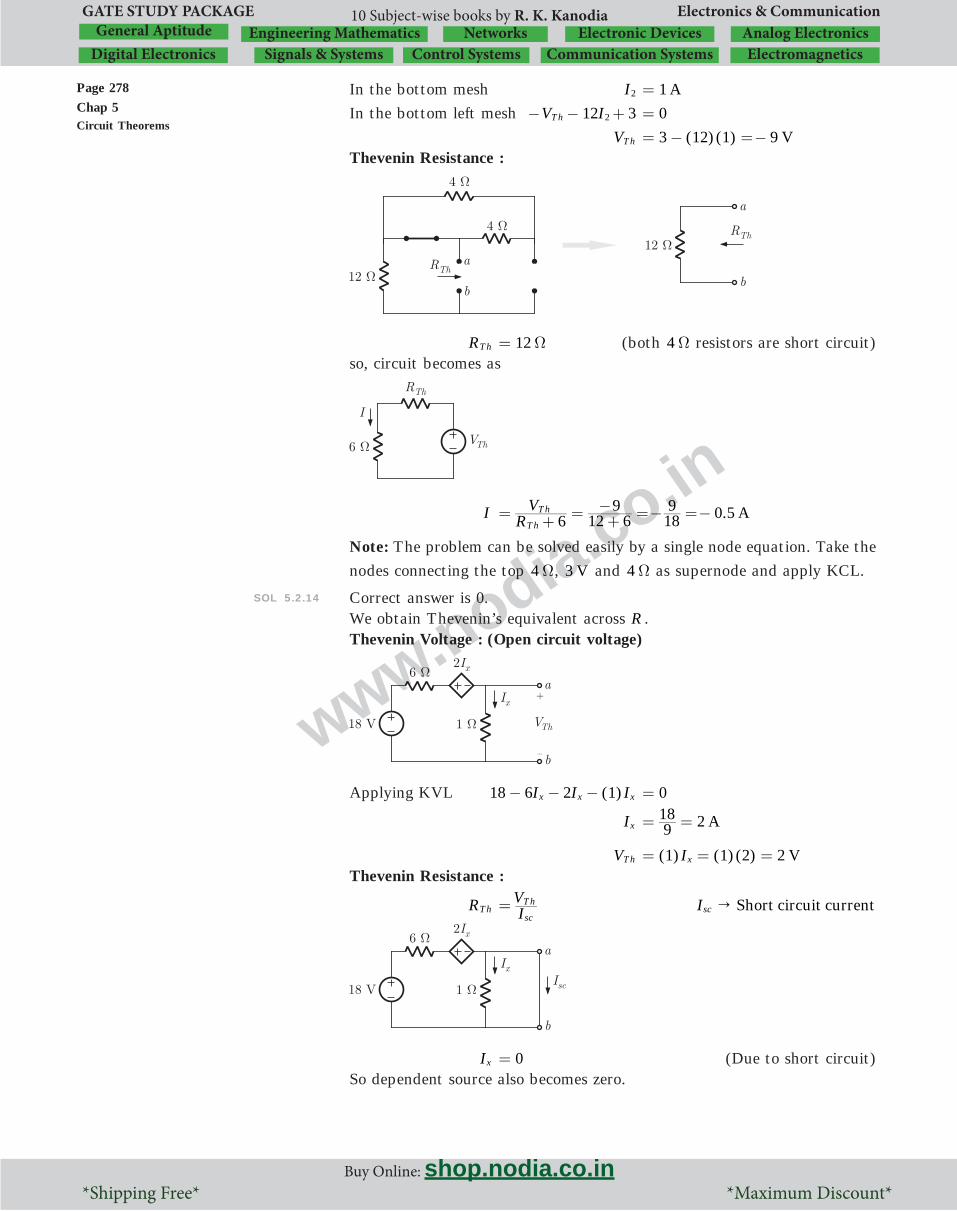
Page 278Chap 5Circuit Theorems
www.nodia.co.in
GATE STUDY PACKAGE Electronics & Communication
Buy Online: shop.nodia.co.in *Shipping Free* *Maximum Discount*
10 Subject-wise books by R. K. KanodiaNetworks Electronic Devices Analog Electronics
Digital Electronics Signals & Systems Control Systems ElectromagneticsCommunication SystemsGeneral Aptitude Engineering Mathematics
In the bottom mesh I2 1 A=In the bottom left mesh V I12 3Th 2- - + 0= VTh 3 (12)(1) 9 V= - =-Thevenin Resistance :
RTh 12 W= (both 4 W resistors are short circuit)so, circuit becomes as
I 0.5 ARV
6 12 69
189
Th
Th= + = +- =- =-
Note: The problem can be solved easily by a single node equation. Take the
nodes connecting the top 4 W, 3 V and 4 W as supernode and apply KCL.
SOL 5.2.14 Correct answer is 0.We obtain Thevenin’s equivalent across R .Thevenin Voltage : (Open circuit voltage)
Applying KVL 18 6 2 (1)I I Ix x x- - - 0=
Ix A918 2= =
VTh (1) (1)(2) 2 VIx= = =Thevenin Resistance :
RTh IV
sc
Th= Short circuit currentIsc "
Ix 0= (Due to short circuit)So dependent source also becomes zero.

Page 279Chap 5
Circuit Theorems
www.nodia.co.in
Buy Online: shop.nodia.co.in *Shipping Free* *Maximum Discount*
GATE STUDY PACKAGE Electronics & Communication
Sample Chapter of Network Analysis (Vol-3, GATE Study Package)
Isc 3 A618= =
Thevenin resistance,
RTh IV
32
sc
Th W= =
Now, the circuit becomes as
I R3
22 3=+
=
2 R2 3= + R 0=
SOL 5.2.15 Correct answer is 121.5 .We obtain Thevenin’s equivalent across R . By source transformation of both voltage sources
Adding parallel sources and combining parallel resistances
Here, VTh 5.4 V= , 60RTh W=For maximum power transfer
R 60RTh W= =

Page 280Chap 5Circuit Theorems
www.nodia.co.in
GATE STUDY PACKAGE Electronics & Communication
Buy Online: shop.nodia.co.in *Shipping Free* *Maximum Discount*
10 Subject-wise books by R. K. KanodiaNetworks Electronic Devices Analog Electronics
Digital Electronics Signals & Systems Control Systems ElectromagneticsCommunication SystemsGeneral Aptitude Engineering Mathematics
Maximum Power absorbed by R
P ( . )
121.5 mWRV4 4 60
5 4Th2 2
#= = =^ h
ALTERNATIVE METHOD : Thevenin voltage (open circuit voltage) may be obtained using node voltage method also.
SOL 5.2.16 Correct answer is 3.First we obtain equivalent voltage and resistance across terminal a -b using Millman’s theorem.
Vab V24151
151
51
1560
15120
520
=+ +
- + - +=-^ h
Rab 1 3
151
151
51 W =
+ +=
So, the circuit is reduced as
I 3 A3 524= + =
SOL 5.2.17 Correct answer is 6.Set all independent sources to zero as shown,
RTh 6 W=
SOL 5.2.18 Correct answer is 0.5 .We solve this problem using linearity and taking assumption that 1 AI = .

Page 281Chap 5
Circuit Theorems
www.nodia.co.in
Buy Online: shop.nodia.co.in *Shipping Free* *Maximum Discount*
GATE STUDY PACKAGE Electronics & Communication
Sample Chapter of Network Analysis (Vol-3, GATE Study Package)
In the circuit, V2 4 4 VI= = (Using Ohm’s law)
I2 I I1= + (Using KCL)
1 1 AV4 8 12
4342= + + = + =
V3 I V3 2 2= + (Using KVL)
3 4 4 8 V3#= + =
Is I I3 2= + (Using KCL)
4 AV I3 38
343
2= + = + =
Applying superposition
When Is 4 A= , 1 AI =
But actually Is 2 A= , So 2 0.5 AI 41#= =
SOL 5.2.19 Correct answer is 1- .Solving with superposition,Due to 6 V Source Only : (Open Circuit 2 mA source)
Is ||0.6 mA
6 6 126
6 46= + = + =
I1 ( )I6 126
s= + .6 0.2 mA186 0#= = (Using current division)
Due to 2 mA source only : (Short circuit 6 V source) :
Combining resistances,
6 || 6k kW W 3 kW= 3 6k kW W+ 9 kW=
I2 ( 2) 1.2 mA9 69= + - =- (Current division)
I I I1 2= + (Using superposition)
0.2 1.2 1 mA= - =-
ALTERNATIVE METHOD :
Try to solve the problem using source conversion.
SOL 5.2.20 Correct answer is 4.We find Thevenin equivalent across a -b .
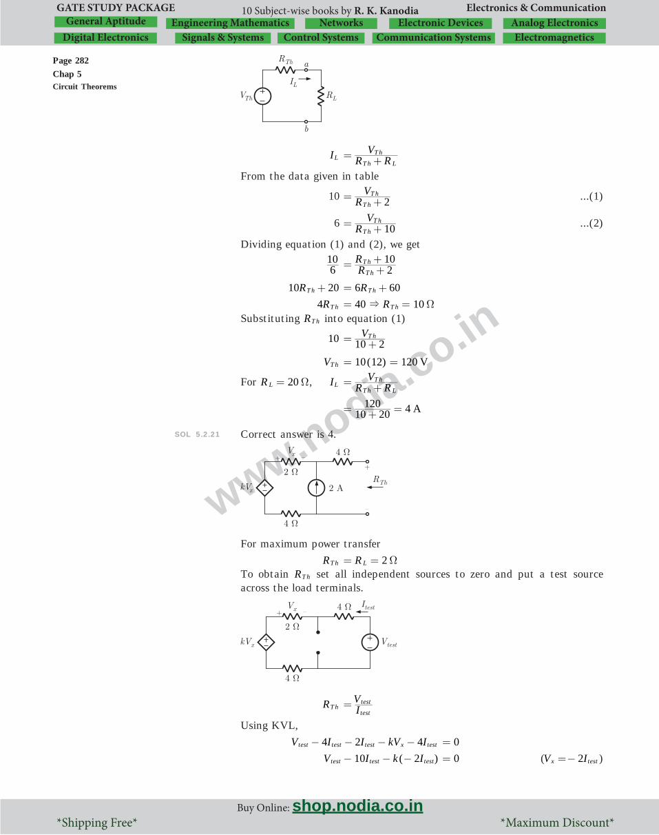
Page 282Chap 5Circuit Theorems
www.nodia.co.in
GATE STUDY PACKAGE Electronics & Communication
Buy Online: shop.nodia.co.in *Shipping Free* *Maximum Discount*
10 Subject-wise books by R. K. KanodiaNetworks Electronic Devices Analog Electronics
Digital Electronics Signals & Systems Control Systems ElectromagneticsCommunication SystemsGeneral Aptitude Engineering Mathematics
IL R RV
Th L
Th= +From the data given in table
10 RV
2Th
Th= + ...(1)
6 RV
10Th
Th= + ...(2)
Dividing equation (1) and (2), we get
610 R
R210
Th
Th= ++
R10 20Th + R6 60Th= + R4 Th 40 10RTh& W= =Substituting RTh into equation (1)
10 V10 2
Th= +
VTh 10(12) 120 V= =
For 20RL W= , IL R RV
Th L
Th= +
A10 20120 4= + =
SOL 5.2.21 Correct answer is 4.
For maximum power transfer
RTh 2RL W= =To obtain RTh set all independent sources to zero and put a test source across the load terminals.
RTh IV
test
test=
Using KVL,
V I I kV I4 2 4test test test x test- - - - 0= ( )V I k I10 2test test test- - - 0= (V I2x test=- )

Page 283Chap 5
Circuit Theorems
www.nodia.co.in
Buy Online: shop.nodia.co.in *Shipping Free* *Maximum Discount*
GATE STUDY PACKAGE Electronics & Communication
Sample Chapter of Network Analysis (Vol-3, GATE Study Package)
Vtest ( )k I10 2 test= -
RTh 10 2IV k 2
test
test= = - =
8 k2= or k 4=
SOL 5.2.22 Correct answer is 18.To calculate maximum power transfer, first we will find Thevenin equivalent across load terminals.Thevenin Voltage: (Open Circuit Voltage)
Using source transformation
VTh ( )2 22 24= + (Using voltage division)
12 V=Thevenin Resistance :
RTh 1 2 || 2 1 1 2 kW= + = + =Circuit becomes as
VL R RR V
Th L
LTh= +
For maximum power transfer R RL Th=
VL RV R V2 2Th
ThTh
Th#= =
So maximum power absorbed by RL

Page 284Chap 5Circuit Theorems
www.nodia.co.in
GATE STUDY PACKAGE Electronics & Communication
Buy Online: shop.nodia.co.in *Shipping Free* *Maximum Discount*
10 Subject-wise books by R. K. KanodiaNetworks Electronic Devices Analog Electronics
Digital Electronics Signals & Systems Control Systems ElectromagneticsCommunication SystemsGeneral Aptitude Engineering Mathematics
Pmax RV
RV4L
L
Th
Th2 2
= = ( )
18 mW4 212 2
#= =
SOL 5.2.23 Correct answer is 22.5 .The circuit is as shown below
When 50RL W= , power absorbed in load will be
50RR I50s
ss
2
+b l 20= kW ...(1)
When 0R 20L W= , power absorbed in load will be
200RR I200s
ss
2
+b l 20= kW ...(2)
Dividing equation (1) and (2), we have
( 200)Rs2+ 4( 50)Rs
2= + Rs 100 W= and 30 AIs =From maximum power transfer, the power supplied by source current Is will
be maximum when load resistance is equal to source resistance i.e. R RL s=. Maximum power is given as
Pmax ( )
22.5I R4 4
30 1002s s
2#= = = kW
SOL 5.2.24 Correct answer is 6.If we solve this circuit directly by nodal analysis, then we have to deal with three variables. We can replace the left most and write most circuit by their Thevenin equivalent as shown below.
Now the circuit becomes as shown
Writing node equation at the top center node
V V V1 1
46 1 2
121 1 1+- + + +
- 0=

Page 285Chap 5
Circuit Theorems
www.nodia.co.in
Buy Online: shop.nodia.co.in *Shipping Free* *Maximum Discount*
GATE STUDY PACKAGE Electronics & Communication
Sample Chapter of Network Analysis (Vol-3, GATE Study Package)
V V V2
46 3
121 1 1+ + + - 0=
V V V3 12 2 2411 1- + + - 0= V6 1 36= V1 6 V=
SOL 5.2.25 Correct answer is 56.6 W and 3 W resistors are in parallel, which is equivalent to 2 W.
Using source transformation of 6 A source
Source transform of 4 A source
Adding series resistors and sources on the left
Source transformation of 48 V source

Page 286Chap 5Circuit Theorems
www.nodia.co.in
GATE STUDY PACKAGE Electronics & Communication
Buy Online: shop.nodia.co.in *Shipping Free* *Maximum Discount*
10 Subject-wise books by R. K. KanodiaNetworks Electronic Devices Analog Electronics
Digital Electronics Signals & Systems Control Systems ElectromagneticsCommunication SystemsGeneral Aptitude Engineering Mathematics
Source transformation of 4 A3 source.
I V19 9
12 72 s= ++ +
Vs (28 ) 12 72I#= - - (28 5) 12 72#= - - 56 V=
SOL 5.2.26 Correct answer is 0.5 .We obtain I using superposition.Due to 24 V source only : (Open circuit 6 A)
Applying KVL
I I I24 6 3 31 1 1- - - 0=
I1 2 A1224= =
Due to 6 A source only : (Short circuit 24 V source)
Applying KVL to supermesh
( )I I I6 3 6 32 2 2- - + - 0= I I I6 18 3 32 2 2+ + + 0=
I2 A1218
23=- =-
From superposition, I I I1 2= +
. A2 23
21 0 5= - = =
ALTERNATIVE METHOD : Note that current in 3 W resistor is 6I +^ h A, so by applying KVL around the outer loop, we can find current I .
SOL 5.2.27 Correct answer is 11.
RTh short circuitOpen circuit voltage
IV
sc
oc= =
Thevenin Voltage: (Open Circuit Voltage Voc)Using source transformation of the dependent source

Page 287Chap 5
Circuit Theorems
www.nodia.co.in
Buy Online: shop.nodia.co.in *Shipping Free* *Maximum Discount*
GATE STUDY PACKAGE Electronics & Communication
Sample Chapter of Network Analysis (Vol-3, GATE Study Package)
Applying KCL at top left node
24 144 VV V6x
x&= =
Using KVL, V I V V8 2xx
oc- - - 0=
144 0 2144- - Voc=
Voc 72 V=
Short circuit current (Isc):
Applying KVL in the right mesh
V I V8 2x scx- - 0=
V2x I8 sc=
Vx I16 sc=KCL at the top left node
24 /V V V
6 82x x x= + -
24 V V6 16x x= +
Vx V111152=
Isc AV16 11 16
11521172x
#= = =
RTh IV 72 11
sc
oc
1172 W = = =
ALTERNATIVE METHOD :We can obtain Thevenin equivalent resistance without calculating the Thevenin voltage (open circuit voltage). Set all independent sources to zero (i.e. open circuit current sources and short circuit voltage sources) and put a test source Vtest between terminal a -b as shown

Page 288Chap 5Circuit Theorems
www.nodia.co.in
GATE STUDY PACKAGE Electronics & Communication
Buy Online: shop.nodia.co.in *Shipping Free* *Maximum Discount*
10 Subject-wise books by R. K. KanodiaNetworks Electronic Devices Analog Electronics
Digital Electronics Signals & Systems Control Systems ElectromagneticsCommunication SystemsGeneral Aptitude Engineering Mathematics
RTh IV
test
test=
6 8I I V V2x
test+ - - 0= (KVL)
14I I V26
test- - 0= 6V Ix test= (Using Ohm’s law)
I11 Vtest=
So RTh 11IV
test
test W= =
SOL 5.2.28 Correct answer is 4.We solve this problem using linearity and assumption that 1 AI = .
V1 I I4 2= + (Using KVL)
6 V= I2 I I1= + (Using KCL)
V I41= + 1 2.5 A4
6= + =
V2 I V4 2 1= + (Using KVL)
4(2.5) 6 16 V= + = I Is 3+ I2= (Using KCL)
I V4 12s
2- + I2=
Is 2.5 3.5 A1616= + =
When 3.5 AIs = , I 1 A=
But 14 AIs = , so I .. 14 4 A3 51
#= =
SOL 5.2.29 Correct answer is 120.This problem will easy to solve if we obtain Thevenin equivalent across the 12 V source.Thevenin Voltage : (Open Circuit Voltage)
Mesh currents are
Mesh 1: I1 0= (due to open circuit)
Mesh 2: I I1 3- 2= or 2 AI3 =-Mesh 3: I I3 2- 4= or 6 AI2 =-Mesh equation for outer loop

Page 289Chap 5
Circuit Theorems
www.nodia.co.in
Buy Online: shop.nodia.co.in *Shipping Free* *Maximum Discount*
GATE STUDY PACKAGE Electronics & Communication
Sample Chapter of Network Analysis (Vol-3, GATE Study Package)
V I I1 1Th 3 2# #- - 0= ( ) ( )V 2 6Th - - - - 0= V 2 6Th + + 0= VTh 8 V=-Thevenin Resistance :
RTh 1 1 2 W= + =circuit becomes as
I ( )
10 ARV12
212 8
Th
Th= - = - - =
Power supplied by 12 V source
P12 V 10 12 120 W#= =
ALTERNATIVE METHOD :
KVL in the loop ABCDA
( ) ( )I I12 1 2 1 6- - - - 0= I2 20= I 10 A=Power supplied by 12 V source
P12 V 10 12 120 W#= =
SOL 5.2.30 Correct answer is 286.For maximum power transfer R RL Th= . To obtain Thevenin resistance set all independent sources to zero and put a test source across load terminals.

Page 290Chap 5Circuit Theorems
www.nodia.co.in
GATE STUDY PACKAGE Electronics & Communication
Buy Online: shop.nodia.co.in *Shipping Free* *Maximum Discount*
10 Subject-wise books by R. K. KanodiaNetworks Electronic Devices Analog Electronics
Digital Electronics Signals & Systems Control Systems ElectromagneticsCommunication SystemsGeneral Aptitude Engineering Mathematics
RTh IV
test
test=
Writing KCL at the top center node
2 1k kV V V2test test x+ - Itest= ...(1)
Also, V Vtest x+ 0= (KVL in left mesh)
so Vx Vtest=-Substituting V Vx test=- into equation (1)
2 1( )
k kV V V2test test test+ - -
Itest=
V V6test test+ I2 test=
RTh 286kIV
72
test
test -W W= =
SOL 5.2.31 Correct answer is 4.Redrawing the circuit in Thevenin equivalent form
I RV V
Th
Th= -
or, V R I VTh Th=- + (General form)From the given graph
V I4 8=- +So, by comparing RTh 4 kW= , 8 VVTh =For maximum power transfer R RL Th=Maximum power absorbed by RL
Pmax ( )
4 mWRV4 4 4
8Th
Th2 2
#= = =
SOL 5.2.32 Correct answer is 3.To fine out Thevenin equivalent of the circuit put a test source between node a and b ,
RTh IV
test
test=
Writing node equation at V1
V I V1 1
x1 1a- + Ix=
V2 1 I1 xa= +^ h ...(1)Ix is the branch current in 1 W resistor given as
Ix V V
1test 1= -

Page 291Chap 5
Circuit Theorems
www.nodia.co.in
Buy Online: shop.nodia.co.in *Shipping Free* *Maximum Discount*
GATE STUDY PACKAGE Electronics & Communication
Sample Chapter of Network Analysis (Vol-3, GATE Study Package)
V1 V Itest x= -Substituting V1 into equation (1)
V I2 test x-^ h I1 xa= +^ h
V2 test I3 xa= +^ h
V2 test I3 testa= +^ h I Ix test=^ h
RTh IV
23 3
test
test a= = + =
3 a+ 6= a 3 W=
SOL 5.2.33 Correct answer is 16.We obtain Thevenin equivalent across the load terminalsThevenin Voltage : (Open circuit voltage)
VTh V Va b= -Rotating the circuit, makes it simple
I1 ( )340 60340 40= + 34 A= (Current division)
Va 20 20 34 680 VI1 #= = = (Ohm’s Law)
Similarly, I2 (40) 6 A60 34060= + = (Current division)
Vb 100 100 6 600 VI2 #= = = (Ohm’s Law)
Thevenin voltage VTh 680 600 80 V= - =Thevenin Resistance :
RTh ( ) || ( )16 240 40 20 100= + + +

Page 292Chap 5Circuit Theorems
www.nodia.co.in
GATE STUDY PACKAGE Electronics & Communication
Buy Online: shop.nodia.co.in *Shipping Free* *Maximum Discount*
10 Subject-wise books by R. K. KanodiaNetworks Electronic Devices Analog Electronics
Digital Electronics Signals & Systems Control Systems ElectromagneticsCommunication SystemsGeneral Aptitude Engineering Mathematics
( || )16 280 120= + 16 84= + 100 W=Now, circuit reduced as
For maximum power transfer
RL 100RTh W= =Maximum power transferred to RL
Pmax ( ) ( )
RV4 4 100
80L
Th2 2
#= = 16 W=
SOL 5.2.34 Correct answer is 108.We use source transformation as follows
I 3 A6 236 12= +
- =
Power supplied by 36 V source
P36 V 3 36 108 W#= =
SOL 5.2.35 Correct answer is 1026.Now, we do source transformation from left to right as shown

Page 293Chap 5
Circuit Theorems
www.nodia.co.in
Buy Online: shop.nodia.co.in *Shipping Free* *Maximum Discount*
GATE STUDY PACKAGE Electronics & Communication
Sample Chapter of Network Analysis (Vol-3, GATE Study Package)
Vs (27 1.5)(4 || 2 )W W= +
.28 5 34
#=
38 V=
Power supplied by 27 A source
P27 A V 27 38 27s # #= =
1026 W=
SOL 5.2.36 Correct answer is 9.First, we find current I in the 4 W resistors using superposition.Due to 18 V source only : (Open circuit 4 A and short circuit 12 V source)
I1 4.5 A418= =
Due to 1 V2 source only : (Open circuit 4 A and short circuit 18 V source)

Page 294Chap 5Circuit Theorems
www.nodia.co.in
GATE STUDY PACKAGE Electronics & Communication
Buy Online: shop.nodia.co.in *Shipping Free* *Maximum Discount*
10 Subject-wise books by R. K. KanodiaNetworks Electronic Devices Analog Electronics
Digital Electronics Signals & Systems Control Systems ElectromagneticsCommunication SystemsGeneral Aptitude Engineering Mathematics
I2 3 A412=- =-
Due to 4 A source only : (Short circuit 12 V and 18 V sources)
I3 0= (Due to short circuit)
So, I I I I1 2 3= + +
.4 5 3 0= - +
1.5 A=Power dissipated in 4 W resistor
P4 W ( ) ( . )I 4 1 5 42 2#= = 9 W=
Alternate Method: Let current in 4 W resistor is I , then by applying KVL
around the outer loop
I18 12 4- - 0=
I 1.5 A46= =
So, power dissipated in 4 W resistor
P4 W ( ) ( . )I 4 1 5 42 2#= =
9 W=
SOL 5.2.37 Correct answer is 10- .Using, Thevenin equivalent circuitThevenin Voltage : (Open Circuit Voltage)
Ix 4 A=- (due to open circuit)Writing KVL in bottom right mesh
( )I V24 1 x Th- - - 0= VTh 24 4 20 V=- + =-Thevenin Resistance :
RTh short circuit currentopen circuit voltage
IV
sc
oc= =
Voc 20 VVTh= =-Isc is obtained as follows

Page 295Chap 5
Circuit Theorems
www.nodia.co.in
Buy Online: shop.nodia.co.in *Shipping Free* *Maximum Discount*
GATE STUDY PACKAGE Electronics & Communication
Sample Chapter of Network Analysis (Vol-3, GATE Study Package)
Ix 24 A124=- =-
I 4x + Isc= (using KCL)
24 4- + Isc= Isc 20 A=-
RTh 12020 W= -
- =
The circuit is as shown below
V ( )R V11
ThTh= + ( )1 1
1 20= + - 10 volt=- (Using voltage division)
ALTERNATIVE METHOD :
Note that current in bottom right most 1 W resistor is I 4x +^ h, so applying
KVL around the bottom right mesh,
4I I24 x x- - - +^ h 0= Ix 14 A=-So, V 1 14 4 10 VI 4x#= + =- + =-^ h
SOL 5.2.38 Correct answer is 100.Writing currents into 100 W and 300 W resistors by using KCL as shown in figure.
Ix 1= A, V Vx test=Writing mesh equation for bottom right mesh.
Vtest 100(1 2 ) 300(1 2 0.01 ) 800I I Vx x x= - + - - + 100= V

Page 296Chap 5Circuit Theorems
www.nodia.co.in
GATE STUDY PACKAGE Electronics & Communication
Buy Online: shop.nodia.co.in *Shipping Free* *Maximum Discount*
10 Subject-wise books by R. K. KanodiaNetworks Electronic Devices Analog Electronics
Digital Electronics Signals & Systems Control Systems ElectromagneticsCommunication SystemsGeneral Aptitude Engineering Mathematics
RTh 100V1test W= =
SOL 5.2.39 Correct answer is 30.
For 10 kRL W= , Vab1 610k 3.6m#= = V
For 30 kRL W= , Vab2 1230k 4.8m#= = V
Vab1 R V1010 6
ThTh= + = ...(1)
Vab2 12R V3030
ThTh= + = ...(2)
Dividing equation (1) and (2), we get RTh 30 kW= . Maximum power will be
transferred when 30 kR RL Th W= = .
***********

Eighth Edition
GATEELECTRONICS & COMMUNICATION
Signals and SystemsVol 7 of 10
RK Kanodia Ashish Murolia
NODIA & COMPANY

GATE Electronics & Communication Vol 7, 8eSignals and SystemsRK Kanodia & Ashish Murolia
Copyright © By NODIA & COMPANY
Information contained in this book has been obtained by author, from sources believes to be reliable. However, neither NODIA & COMPANY nor its author guarantee the accuracy or completeness of any information herein, and NODIA & COMPANY nor its author shall be responsible for any error, omissions, or damages arising out of use of this information. This book is published with the understanding that NODIA & COMPANY and its author are supplying information but are not attempting to render engineering or other professional services.
MRP 690.00
NODIA & COMPANYB 8, Dhanshree Ist, Central Spine, Vidyadhar Nagar, Jaipur 302039Ph : +91 141 2101150, www.nodia.co.inemail : [email protected]
Printed by Nodia and Company, Jaipur

Preface to the Series
For almost a decade, we have been receiving tremendous responses from GATE aspirants for our earlier books: GATE Multiple Choice Questions, GATE Guide, and the GATE Cloud series. Our first book, GATE Multiple Choice Questions (MCQ), was a compilation of objective questions and solutions for all subjects of GATE Electronics & Communication Engineering in one book. The idea behind the book was that Gate aspirants who had just completed or about to finish their last semester to achieve his or her B.E/B.Tech need only to practice answering questions to crack GATE. The solutions in the book were presented in such a manner that a student needs to know fundamental concepts to understand them. We assumed that students have learned enough of the fundamentals by his or her graduation. The book was a great success, but still there were a large ratio of aspirants who needed more preparatory materials beyond just problems and solutions. This large ratio mainly included average students.
Later, we perceived that many aspirants couldn’t develop a good problem solving approach in their B.E/B.Tech. Some of them lacked the fundamentals of a subject and had difficulty understanding simple solutions. Now, we have an idea to enhance our content and present two separate books for each subject: one for theory, which contains brief theory, problem solving methods, fundamental concepts, and points-to-remember. The second book is about problems, including a vast collection of problems with descriptive and step-by-step solutions that can be understood by an average student. This was the origin of GATE Guide (the theory book) and GATE Cloud (the problem bank) series: two books for each subject. GATE Guide and GATE Cloud were published in three subjects only.
Thereafter we received an immense number of emails from our readers looking for a complete study package for all subjects and a book that combines both GATE Guide and GATE Cloud. This encouraged us to present GATE Study Package (a set of 10 books: one for each subject) for GATE Electronic and Communication Engineering. Each book in this package is adequate for the purpose of qualifying GATE for an average student. Each book contains brief theory, fundamental concepts, problem solving methodology, summary of formulae, and a solved question bank. The question bank has three exercises for each chapter: 1) Theoretical MCQs, 2) Numerical MCQs, and 3) Numerical Type Questions (based on the new GATE pattern). Solutions are presented in a descriptive and step-by-step manner, which are easy to understand for all aspirants.
We believe that each book of GATE Study Package helps a student learn fundamental concepts and develop problem solving skills for a subject, which are key essentials to crack GATE. Although we have put a vigorous effort in preparing this book, some errors may have crept in. We shall appreciate and greatly acknowledge all constructive comments, criticisms, and suggestions from the users of this book. You may write to us at [email protected] and [email protected].
Acknowledgements
We would like to express our sincere thanks to all the co-authors, editors, and reviewers for their efforts in making this project successful. We would also like to thank Team NODIA for providing professional support for this project through all phases of its development. At last, we express our gratitude to God and our Family for providing moral support and motivation.
We wish you good luck ! R. K. KanodiaAshish Murolia

SYLLABUS
GATE Electronics & Communications:Definitions and properties of Laplace transform, continuous-time and discrete-time Fourier series, continuous-time and discrete-time Fourier Transform, DFT and FFT, z-transform. Sampling theorem. Linear Time-Invariant (LTI) Systems: definitions and properties; causality, stability, impulse response, convolution, poles and zeros, parallel and cascade structure, frequency response, group delay, phase delay. Signal transmission through LTI systems.
IES Electronics & Telecommunication
Classification of signals and systems: System modelling in terms of differential and difference equations; State variable representation; Fourier series; Fourier transforms and their application to system analysis; Laplace transforms and their application to system analysis; Convolution and superposition integrals and their applications; Z-transforms and their applications to the analysis and characterisation of discrete time systems; Random signals and probability, Correlation functions; Spectral density; Response of linear system to random inputs.
**********

CONTENTS
CHAPTER 1 CONTINUOUS TIME SIGNALS
1.1 CONTINUOUS - TIME AND DISCRETE - TIME SIGNALS 1
1.2 SIGNAL-CLASSIFICATION 1
1.2.1 Analog and Discrete Signals 1
1.2.2 Deterministic and Random Signal 1
1.2.3 Periodic and Aperiodic Signal 2
1.2.4 Even and Odd Signal 3
1.2.5 Energy and Power Signal 4
1.3 BASIC OPERATIONS ON SIGNALS 5
1.3.1 Addition of Signals 5
1.3.2 Multiplication of Signals 5
1.3.3 Amplitude Scaling of Signals 5
1.3.4 Time-Scaling 5
1.3.5 Time-Shifting 6
1.3.6 Time-Reversal/Folding 7
1.3.7 Amplitude Inverted Signals 8
1.4 MULTIPLE OPERATIONS ON SIGNALS 8
1.5 BASIC CONTINUOUS TIME SIGNALS 9
1.5.1 The Unit-Impulse Function 9
1.5.2 The Unit-Step Function 12
1.5.3 The Unit-Ramp Function 12
1.5.4 Unit Rectangular Pulse Function 13
1.5.5 Unit Triangular Function 13
1.5.6 Unit Signum Function 14
1.5.7 The Sinc Function 14
1.6 MATHEMATICAL REPRESENTATION OF SIGNALS 15
EXERCISE 1.1 16
EXERCISE 1.2 41
EXERCISE 1.3 44
EXERCISE 1.4 49
SOLUTIONS 1.1 56
SOLUTIONS 1.2 79
SOLUTIONS 1.3 84
SOLUTIONS 1.4 85

CHAPTER 2 CONTINUOUS TIME SYSTEMS
2.1 CONTINUOUS TIME SYSTEM & CLASSIFICATION 93
2.1.1 Linear and Non-Linear System 93
2.1.2 Time-Varying and Time-Invariant system 93
2.1.3 Systems With and Without Memory (Dynamic and Static Systems) 94
2.1.4 Causal and Non-causal Systems 94
2.1.5 Invertible and Non-Invertible Systems 94
2.1.6 Stable and Unstable systems 94
2.2 LINEAR TIME INVARIANT SYSTEM 95
2.2.1 Impulse Response and The Convolution Integral 95
2.2.2 Properties of Convolution Integral 96
2.3 STEP RESPONSE OF AN LTI SYSTEM 100
2.4 PROPERTIES OF LTI SYSTEMS IN TERMS OF IMPULSE RESPONSE 101
2.4.1 Memoryless LTI System 101
2.4.2 Causal LTI System 101
2.4.3 Invertible LTI System 102
2.4.4 Stable LTI System 102
2.5 IMPULSE RESPONSE OF INTER-CONNECTED SYSTEMS 103
2.5.1 Systems in Parallel Configuration 103
2.5.2 System in Cascade 103
2.6 CORRELATION 103
2.6.1 Cross-Correlation 103
2.6.2 Auto-Correlation 105
2.6.3 Correlation and Convolution 109
2.7 TIME DOMAIN ANALYSIS OF CONTINUOUS TIME SYSTEMS 109
2.7.1 Natural Response or Zero-input Response 110
2.7.2 Forced Response or Zero-state Response 111
2.7.3 The Total Response 111
2.8 BLOCK DIAGRAM REPRESENTATION 112
EXERCISE 2.1 114
EXERCISE 2.2 133
EXERCISE 2.3 135
EXERCISE 2.4 138
SOLUTIONS 2.1 149
SOLUTIONS 2.2 179
SOLUTIONS 2.3 186
SOLUTIONS 2.4 187
CHAPTER 3 DISCRETE TIME SIGNALS
3.1 INTRODUCTION TO DISCRETE TIME SIGNALS 203
3.1.1 Representation of Discrete Time signals 203

3.2 SIGNAL CLASSIFICATION 204
3.2.1 Periodic and Aperiodic DT Signals 204
3.2.2 Even and Odd DT Signals 205
3.2.3 Energy and Power Signals 207
3.3 BASIC OPERATIONS ON DT SIGNALS 207
3.3.1 Addition of DT Signals 208
3.3.2 Multiplication of DT Signal 208
3.3.3 Amplitude scaling of DT Signals 208
3.3.4 Time-Scaling of DT Signals 208
3.3.5 Time-Shifting of DT Signals 209
3.3.6 Time-Reversal (folding) of DT signals 210
3.3.7 Inverted DT Signals 211
3.4 MULTIPLE OPERATIONS ON DT SIGNALS 211
3.5 BASIC DISCRETE TIME SIGNALS 212
3.5.1 Discrete Impulse Function 212
3.5.2 Discrete Unit Step Function 213
3.5.3 Discrete Unit-ramp Function 213
3.5.4 Unit-Rectangular Function 214
3.5.5 Unit-Triangular Function 214
3.5.6 Unit-Signum Function 215
3.6 MATHEMATICAL REPRESENTATION OF DT SIGNALS USING IMPULSE OR STEP FUNCTION 215
EXERCISE 3.1 216
EXERCISE 3.2 241
EXERCISE 3.3 244
EXERCISE 3.4 247
SOLUTIONS 3.1 249
SOLUTIONS 3.2 273
SOLUTIONS 3.3 281
SOLUTIONS 3.4 282
CHAPTER 4 DISCRETE TIME SYSTEMS
4.1 DISCRETE TIME SYSTEM & CLASSIFICATION 285
4.1.1 Linear and Non-linear Systems 285
4.1.2 Time-Varying and Time-Invariant Systems 285
4.1.3 System With and Without Memory (Static and Dynamic Systems) 286
4.1.4 Causal and Non-Causal System 286
4.1.5 Invertible and Non-Invertible Systems 286
4.1.6 Stable and Unstable System 286
4.2 LINEAR-TIME INVARIANT DISCRETE SYSTEM 287
4.2.1 Impulse Response and Convolution Sum 287
4.2.2 Properties of Convolution Sum 288
4.3 STEP RESPONSE OF AN LTI SYSTEM 292

4.4 PROPERTIES OF DISCRETE LTI SYSTEM IN TERMS OF IMPULSE RESPONSE 292
4.4.1 Memoryless LTID System 293
4.4.2 Causal LTID System 293
4.4.3 Invertible LTID System 293
4.4.4 Stable LTID System 294
4.4.5 FIR and IIR Systems 294
4.5 IMPULSE RESPONSE OF INTERCONNECTED SYSTEMS 295
4.5.1 Systems in Parallel 295
4.5.2 System in Cascade 295
4.6 CORRELATION 296
4.6.1 Cross-Correlation 296
4.6.2 Auto-Correlation 296
4.6.3 Properties of Correlation 297
4.6.4 Relationship Between Correlation and Convolution 299
4.6.5 Methods to Solve Correlation 299
4.7 DECONVOLUTION 300
4.8 RESPONSE OF LTID SYSTEMS IN TIME DOMAIN 300
4.8.1 Natural Response or Zero Input Response 301
4.8.2 Forced Response or Zero State Response 302
4.8.3 Total Response 302
4.9 BLOCK DIAGRAM REPRESENTATION 303
EXERCISE 4.1 304
EXERCISE 4.2 317
EXERCISE 4.3 320
EXERCISE 4.4 323
SOLUTIONS 4.1 329
SOLUTIONS 4.2 353
SOLUTIONS 4.3 361
SOLUTIONS 4.4 362
CHAPTER 5 THE LAPLACE TRANSFORM
5.1 INTRODUCTION 375
5.1.1 The Bilateral or Two-Sided Laplace Transform 375
5.1.2 The Unilateral Laplace Transform 375
5.2 THE EXISTENCE OF LAPLACE TRANSFORM 375
5.3 REGION OF CONVERGENCE 376
5.3.1 Poles and Zeros of Rational Laplace Transforms 376
5.3.2 Properties of ROC 377
5.4 THE INVERSE LAPLACE TRANSFORM 382
5.4.1 Inverse Laplace Transform Using Partial Fraction Method 383
5.4.2 Inverse Laplace Transform Using Convolution Method 383

5.5 PROPERTIES OF THE LAPLACE TRANSFORM 384
5.5.1 Linearity 384
5.5.2 Time Scaling 384
5.5.3 Time Shifting 385
5.5.4 Shifting in the s -domain(Frequency Shifting) 386
5.5.5 Time Differentiation 386
5.5.6 Time Integration 387
5.5.7 Differentiation in the s -domain 388
5.5.8 Conjugation Property 389
5.5.9 Time Convolution 389
5.5.10 s -Domain Convolution 390
5.5.11 Initial value Theorem 390
5.5.12 Final Value Theorem 391
5.5.13 Time Reversal Property 391
5.6 ANALYSIS OF CONTINUOUS LTI SYSTEMS USING LAPLACE TRANSFORM 393
5.6.1 Response of LTI Continuous Time System 393
5.6.2 Impulse Response and Transfer Function 394
5.7 STABILITY AND CAUSALITY OF CONTINUOUS LTI SYSTEM USING LAPLACE TRANSFORM 394
5.7.1 Causality 395
5.7.2 Stability 395
5.7.3 Stability and Causality 395
5.8 SYSTEM FUNCTION FOR INTERCONNECTED LTI SYSTEMS 395
5.8.1 Parallel Connection 395
5.8.2 Cascaded Connection 396
5.8.3 Feedback Connection 396
5.9 BLOCK DIAGRAM REPRESENTATION OF CONTINUOUS LTI SYSTEM 397
5.9.1 Direct Form I structure 397
5.9.2 Direct Form II structure 399
5.9.3 Cascade Structure 401
5.9.4 Parallel Structure 402
EXERCISE 5.1 404
EXERCISE 5.2 417
EXERCISE 5.3 422
EXERCISE 5.4 426
SOLUTIONS 5.1 442
SOLUTIONS 5.2 461
SOLUTIONS 5.3 473
SOLUTIONS 5.4 474
CHAPTER 6 THE Z-TRANSFORM
6.1 INTRODUCTION 493
6.1.1 The Bilateral or Two-Sided z -transform 493

6.1.2 The Unilateral or One-sided z -transform 494
6.2 EXISTENCE OF z-TRANSFORM 494
6.3 REGION OF CONVERGENCE 494
6.3.1 Poles and Zeros of Rational z -transforms 494
6.3.2 Properties of ROC 495
6.4 THE INVERSE z-TRANSFORM 500
6.4.1 Partial Fraction Method 502
6.4.2 Power Series Expansion Method 503
6.5 PROPERTIES OF z-TRANSFORM 503
6.5.1 Linearity 503
6.5.2 Time Shifting 504
6.5.3 Time Reversal 505
6.5.4 Differentiation in the z -domain 506
6.5.5 Scaling in z -Domain 506
6.5.6 Time Scaling 506
6.5.7 Time Differencing 507
6.5.8 Time Convolution 508
6.5.9 Conjugation Property 508
6.5.10 Initial Value Theorem 509
6.5.11 Final Value Theorem 509
6.6 ANALYSIS OF DISCRETE LTI SYSTEMS USING z-TRANSFORM 511
6.6.1 Response of LTI Continuous Time System 511
6.6.2 Impulse Response and Transfer Function 512
6.7 STABILITY AND CAUSALITY OF LTI DISCRETE SYSTEMS USING z-TRANSFORM 513
6.7.1 Causality 513
6.7.2 Stability 513
6.7.3 Stability and Causality 514
6.8 BLOCK DIAGRAM REPRESENTATION 514
6.8.1 Direct Form I Realization 515
6.8.2 Direct Form II Realization 516
6.8.3 Cascade Form 517
6.8.4 Parallel Form 518
6.9 RELATIONSHIP BETWEEN s-PLANE & z-PLANE 518
EXERCISE 6.1 520
EXERCISE 6.2 536
EXERCISE 6.3 538
EXERCISE 6.4 541
SOLUTIONS 6.1 554
SOLUTIONS 6.2 580
SOLUTIONS 6.3 586
SOLUTIONS 6.4 587

CHAPTER 7 THE CONTINUOUS TIME FOURIER TRANSFORM
7.1 DEFINITION 607
7.1.1 Magnitude and Phase Spectra 607
7.1.2 Existence of Fourier transform 607
7.1.3 Inverse Fourier Transform 608
7.2 SPECIAL FORMS OF FOURIER TRANSFORM 608
7.2.1 Real-valued Even Symmetric Signal 608
7.2.2 Real-valued Odd Symmetric Signal 610
7.2.3 Imaginary-valued Even Symmetric Signal 610
7.2.4 Imaginary-valued Odd Symmetric Signal 611
7.3 PROPERTIES OF FOURIER TRANSFORM 612
7.3.1 Linearity 612
7.3.2 Time Shifting 612
7.3.3 Conjugation and Conjugate Symmetry 612
7.3.4 Time Scaling 613
7.3.5 Differentiation in Time-Domain 614
7.3.6 Integration in Time-Domain 614
7.3.7 Differentiation in Frequency Domain 615
7.3.8 Frequency Shifting 615
7.3.9 Duality Property 615
7.3.10 Time Convolution 616
7.3.11 Frequency Convolution 616
7.3.12 Area Under ( )x t 617
7.3.13 Area Under ( )X jw 617
7.3.14 Parseval’s Energy Theorem 618
7.3.15 Time Reversal 618
7.3.16 Other Symmetry Properties 619
7.4 ANALYSIS OF LTI CONTINUOUS TIME SYSTEM USING FOURIER TRANSFORM 620
7.4.1 Transfer Function & Impulse Response of LTI Continuous System 620
7.4.2 Response of LTI Continuous system using Fourier Transform 620
7.5 RELATION BETWEEN FOURIER AND LAPLACE TRANSFORM 621
EXERCISE 7.1 622
EXERCISE 7.2 634
EXERCISE 7.3 641
EXERCISE 7.4 645
SOLUTIONS 7.1 658
SOLUTIONS 7.2 672
SOLUTIONS 7.3 688
SOLUTIONS 7.4 689
CHAPTER 8 THE DISCRETE TIME FOURIER TRANSFORM
8.1 DEFINITION 705

8.1.1 Magnitude and Phase Spectra 705
8.1.2 Existence of DTFT 705
8.1.3 Inverse DTFT 705
8.2 SPECIAL FORMS OF DTFT 706
8.3 PROPERTIES OF DISCRETE-TIME FOURIER TRANSFORM 707
8.3.1 Linearity 707
8.3.2 Periodicity 707
8.3.3 Time Shifting 708
8.3.4 Frequency Shifting 708
8.3.5 Time Reversal 708
8.3.6 Time Scaling 709
8.3.7 Differentiation in Frequency Domain 710
8.3.8 Conjugation and Conjugate Symmetry 710
8.3.9 Convolution in Time Domain 711
8.3.10 Convolution in Frequency Domain 711
8.3.11 Time Differencing 712
8.3.12 Time Accumulation 712
8.3.13 Parseval’s Theorem 713
8.4 ANALYSIS OF LTI DISCRETE TIME SYSTEM USING DTFT 714
8.4.1 Transfer Function & Impulse Response 714
8.4.2 Response of LTI DT system using DTFT 714
8.5 RELATION BETWEEN THE DTFT & THE Z-TRANSFORM 715
8.6 DISCRETE FOURIER TRANSFORM (DFT) 715
8.6.1 Inverse Discrete Fourier Transform (IDFT) 716
8.7 PROPERTIES OF DFT 716
8.7.1 Linearity 716
8.7.2 Periodicity 717
8.7.3 Conjugation and Conjugate Symmetry 717
8.7.4 Circular Time Shifting 718
8.7.5 Circular Frequency Shift 719
8.7.6 Circular Convolution 719
8.7.7 Multiplication 720
8.7.8 Parseval’s Theorem 721
8.7.9 Other Symmetry Properties 721
8.8 FAST FOURIER TRANSFORM (FFT) 722
EXERCISE 8.1 724
EXERCISE 8.2 735
EXERCISE 8.3 739
EXERCISE 8.4 742
SOLUTIONS 8.1 746
SOLUTIONS 8.2 760
SOLUTIONS 8.3 769

SOLUTIONS 8.4 770
CHAPTER 9 THE CONTINUOUS TIME FOURIER SERIES
9.1 INTRODUCTION TO CTFS 775
9.1.1 Trigonometric Fourier Series 775
9.1.2 Exponential Fourier Series 778
9.1.3 Polar Fourier Series 779
9.2 EXISTENCE OF FOURIER SERIES 780
9.3 PROPERTIES OF EXPONENTIAL CTFS 780
9.3.1 Linearity 780
9.3.2 Time Shifting 781
9.3.3 Time Reversal Property 781
9.3.4 Time Scaling 782
9.3.5 Multiplication 782
9.3.6 Conjugation and Conjugate Symmetry 783
9.3.7 Differentiation Property 783
9.3.8 Integration in Time-Domain 784
9.3.9 Convolution Property 784
9.3.10 Parseval’s Theorem 785
9.3.11 Frequency Shifting 786
9.4 AMPLITUDE & PHASE SPECTRA OF PERIODIC SIGNAL 787
9.5 RELATION BETWEEN CTFT & CTFS 787
9.5.1 CTFT using CTFS Coefficients 787
9.5.2 CTFS Coefficients as Samples of CTFT 787
9.6 RESPONSE OF AN LTI CT SYSTEM TO PERIODIC SIGNALS USING FOURIER SERIES 788
EXERCISE 9.1 790
EXERCISE 9.2 804
EXERCISE 9.3 806
EXERCISE 9.4 811
SOLUTIONS 9.1 824
SOLUTIONS 9.2 840
SOLUTIONS 9.3 844
SOLUTIONS 9.4 845
CHAPTER 10 THE DISCRETE TIME FOURIER SERIES
10.1 DEFINITION 861
10.2 AMPLITUDE AND PHASE SPECTRA OF PERIODIC DT SIGNALS 861
10.3 PROPERTIES OF DTFS 861
10.3.1 Linearity 862
10.3.2 Periodicity 862
10.3.3 Time-Shifting 862

10.3.4 Frequency Shift 863
10.3.5 Time-Reversal 863
10.3.6 Multiplication 864
10.3.7 Conjugation and Conjugate Symmetry 864
10.3.8 Difference Property 865
10.3.9 Parseval’s Theorem 865
10.3.10 Convolution 866
10.3.11 Duality 867
10.3.12 Symmetry 867
10.3.13 Time Scaling 867
EXERCISE 10.1 870
EXERCISE 10.2 880
EXERCISE 10.3 882
EXERCISE 10.4 884
SOLUTIONS 10.1 886
SOLUTIONS 10.2 898
SOLUTIONS 10.3 903
SOLUTIONS 10.4 904
CHAPTER 11 SAMPLING AND SIGNAL RECONSTRUCTION
11.1 THE SAMPLING PROCESS 905
11.2 THE SAMPLING THEOREM 905
11.3 IDEAL OR IMPULSE SAMPLING 905
11.4 NYQUIST RATE OR NYQUIST INTERVAL 907
11.5 ALIASING 907
11.6 SIGNAL RECONSTRUCTION 908
11.7 SAMPLING OF BAND-PASS SIGNALS 909
EXERCISE 11.1 911
EXERCISE 11.2 919
EXERCISE 11.3 922
EXERCISE 11.4 925
SOLUTIONS 11.1 928
SOLUTIONS 11.2 937
SOLUTIONS 11.3 941
SOLUTIONS 11.4 942
***********

Page 493Chap 6
The Z-Transform
www.nodia.co.in
Buy Online: shop.nodia.co.in *Shipping Free* *Maximum Discount*
GATE STUDY PACKAGE Electronics & Communication
Sample Chapter of Signals and Systems (Vol-7, GATE Study Package)
6.1 INTRODUCTION
As we studied in previous chapter, the Laplace transform is an important tool for analysis of continuous time signals and systems. Similarly, z -transforms enables us to analyze discrete time signals and systems in the z -domain.
Like, the Laplace transform, it is also classified as bilateral z -transform and unilateral z -transform.
The bilateral or two-sided z -transform is used to analyze both causal and non-causal LTI discrete systems, while the unilateral z -transform is defined only for causal signals.
NOTE :The properties of z -transform are similar to those of the Laplace transform.
6.1.1 The Bilateral or Two-Sided z -transform
The z -transform of a discrete-time sequence [ ]x n , is defined as
( )X z { [ ]} [ ]x n x n zZ n
n
= =3
3-
=-/ (6.1.1)
Where, ( )X z is the transformed signal and Z represents the z-transformation. z is a complex variable. In polar form, z can be expressed as
z rej= W
where r is the magnitude of z and W is the angle of z . This corresponds to a circle in z plane with radius r as shown in figure 6.1.1 below
Figure 6.1.1 z -plane
NOTE :The signal [ ]x n and its z -transform ( )X z are said to form a z -transform pair denoted as
[ ] ( )x n X zZ
CHAPTER 6THE Z-TRANSFORM

Page 494Chap 6The Z-Transform
www.nodia.co.in
GATE STUDY PACKAGE Electronics & Communication
Buy Online: shop.nodia.co.in *Shipping Free* *Maximum Discount*
Networks Electronic Devices Analog ElectronicsDigital Electronics Signals & Systems Control Systems ElectromagneticsCommunication SystemsGeneral Aptitude Engineering Mathematics
10 Subject-wise books by R. K. Kanodia
6.1.2 The Unilateral or One-sided z -transform
The z -transform for causal signals and systems is referred to as the unilateral z -transform. For a causal sequence
[ ]x n 0= , for 0n <Therefore, the unilateral z -transform is defined as
( )X z [ ]x n z n
n 0
=3
-
=/ (6.1.2)
NOTE :For causal signals and systems, the unilateral and bilateral z -transform are the same.
6.2 EXISTENCE OF �-TRANSFORM
Consider the bilateral z -transform given by equation (6.1.1)
[ ]X z [ ]x n z n
n
=3
3-
=-/
The z -transform exists when the infinite sum in above equation converges. For this summation to be converged [ ]x n z n- must be absolutely summable.
Substituting z rej= W
[ ]X z [ ] ( )x n rej n
n
=3
3W -
=-/
or,
[ ]X z { [ ] }x n r en j n
n
=3
3W- -
=-/
Thus for existence of z -transform
( )X z < 3
[ ]x n r n
n 3
3-
=-/ 31 (6.2.1)
6.3 REGION OF CONVERGENCE
The existence of z -transform is given from equation (6.2.1). The values of r for which [ ]x n r n- is absolutely summable is referred to as region of convergence. Since,z rej= W so r z= . Therefore we conclude that the range of values of the variable z for which the sum in equation (6.1.1) converges is called the region of convergence. This can be explained through the following examples.
6.3.1 Poles and Zeros of Rational z -transforms
The most common form of z -transform is a rational function. Let ( )X z be the z -transform of sequence [ ]x n , expressed as a ratio of two polynomials
( )N z and ( )D z .
( )X z ( )( )
D zN z=
The roots of numerator polynomial i.e. values of z for which ( ) 0X z = is referred to as zeros of ( )X z . The roots of denominator polynomial for which
( )X z 3= is referred to as poles of ( )X z . The representation of ( )X z through its poles and zeros in the z -plane is called pole-zero plot of ( )X z .For example consider a rational transfer function ( )X z given as
( )H z z z
z5 62=
- +
( )( )z z
z2 3
= - -

Page 495Chap 6
The Z-Transform
www.nodia.co.in
Buy Online: shop.nodia.co.in *Shipping Free* *Maximum Discount*
GATE STUDY PACKAGE Electronics & Communication
Sample Chapter of Signals and Systems (Vol-7, GATE Study Package)
Now, the zeros of ( )X z are roots of numerator that is z 0= and poles are roots of equation ( )( )z z2 3 0- - = which are given as z 2= and z 3= . The poles and zeros of ( )X z are shown in pole-zero plot of figure 6.3.1.
Figure 6.3.1 Pole-zero plot of X z^ h
NOTE :In pole-zero plot poles are marked by a small cross ‘#’ and zeros are marked by a small dot ‘o’ as shown in figure 6.3.1.
6.3.2 Properties of ROC
The various properties of ROC are summarized as follows. These properties can be proved by taking appropriate examples of different DT signals.
PROPERTY 1
The ROC is a concentric ring in the z -plane centered about the origin.
PROOF :The z -transform is defined as
( )X z [ ]x n z n
n=
3
3-
=-/
Put z rej= W
( ) ( )X z X rej= W [ ]x n r en j n
n=
3
3W- -
=-/
( )X z converges for those values of z for which [ ]x n r n- is absolutely summbable that is
[ ]x n r n
n 3
3-
=-/ < 3
Thus, convergence is dependent only on r , where, r z=The equation z rej= W , describes a circle in z -plane. Hence the ROC will consists of concentric rings centered at zero.
PROPERTY 2
The ROC cannot contain any poles.
PROOF :ROC is defined as the values of z for which z -transform ( )X z converges. We know that ( )X z will be infinite at pole, and, therefore ( )X z does not converge at poles. Hence the region of convergence does not include any pole.

Page 496Chap 6The Z-Transform
www.nodia.co.in
GATE STUDY PACKAGE Electronics & Communication
Buy Online: shop.nodia.co.in *Shipping Free* *Maximum Discount*
Networks Electronic Devices Analog ElectronicsDigital Electronics Signals & Systems Control Systems ElectromagneticsCommunication SystemsGeneral Aptitude Engineering Mathematics
10 Subject-wise books by R. K. Kanodia
PROPERTY 3
If [ ]x n is a finite duration two-sided sequence then the ROC is entire z-plane except at z 0= and z 3= .
PROOF :A sequence which is zero outside a finite interval of time is called ‘finite duration sequence’. Consider a finite duration sequence [ ]x n shown in figure 6.3.2a; [ ]x n is non-zero only for some interval N n N1 2# # .
Figure 6.3.2a A Finite Duration Sequence
The z -transform of [ ]x n is defined as
( )X z [ ]x n z n
n N
N
1
2
= -
=/
This summation converges for all finite values of z . If N1 is negative and N2 is positive, then ( )X z will have both positive and negative powers of z . The negative powers of z becomes unbounded (infinity) if z 0" . Similarly positive powers of z becomes unbounded (infinity) if z " 3. So ROC of
( )X z is entire z -plane except possible z 0= and/or z 3= .
NOTE :Both N1 and N2 can be either positive or negative.
PROPERTY 4
If [ ]x n is a right-sided sequence, and if the circle z r0= is in the ROC, then all values of z for which z r> 0 will also be in the ROC.
PROOF :A sequence which is zero prior to some finite time is called the right-sided sequence. Consider a right-sided sequence [ ]x n shown in figure 6.3.2b; that is; [ ]x n 0= for n N< 1.
Figure 6.3.2b A Right - Sided Sequence

Page 497Chap 6
The Z-Transform
www.nodia.co.in
Buy Online: shop.nodia.co.in *Shipping Free* *Maximum Discount*
GATE STUDY PACKAGE Electronics & Communication
Sample Chapter of Signals and Systems (Vol-7, GATE Study Package)
Let the z -transform of [ ]x n converges for some value of z z ri.e. 0=_ i. From the condition of convergence we can write
[ ]x n z n
n 3
3-
=-/ < 3
[ ]x n r n
n0
3
3-
=-/ < 3
The sequence is right sided, so limits of above summation changes as
[ ]x n r n
n N0
1
3-
=/ < 3 (6.3.1)
Now if we take another value of z as z r 1= with r r<1 0 , then [ ]x n r n1-
decays faster than [ ]x n r n0- for increasing n . Thus we can write
[ ]x n z n
n N1
3-
=/ [ ]x n z r rn n n
n N0 0
1
=3
- -
=/
[ ]x n r rzn
n N
n0
01
=3
-
=
-a k/ (6.3.2)
From equation (6.3.1) we know that [ ]x n r n0- is absolutely summable.
Let, it is bounded by some value Mx , then equation (6.3.2) becomes as
[ ]x n z n
n N1
3-
=/ M r
zx
n
n N 01
#3
-
=a k/ (6.3.3)
The right hand side of above equation converges only if
1 orrz z r> >0
0
Thus, we conclude that if the circle z r0= is in the ROC, then all values of z for which z r> 0 will also be in the ROC. The ROC of a right-sided sequence is illustrated in figure 6.3.2c.
Figure 6.3.2c ROC of a right-sided sequence
PROPERTY 5
If [ ]x n is a left-sided sequence, and if the circle z r0= is in the ROC, then all values of z for which z r< 0 will also be in the ROC.
PROOF :A sequence which is zero after some finite time interval is called a ‘left-sided signal’. Consider a left-sided signal [ ]x n shown in figure 6.3.2d; that is [ ] 0x n = for n N> 2.

Page 498Chap 6The Z-Transform
www.nodia.co.in
GATE STUDY PACKAGE Electronics & Communication
Buy Online: shop.nodia.co.in *Shipping Free* *Maximum Discount*
Networks Electronic Devices Analog ElectronicsDigital Electronics Signals & Systems Control Systems ElectromagneticsCommunication SystemsGeneral Aptitude Engineering Mathematics
10 Subject-wise books by R. K. Kanodia
Figure 6.3.2d A left-sided sequence
Let z -transform of [ ]x n converges for some values of z . .i e z r0=_ i. From the condition of convergence we write
[ ]x n z n
n 3
3-
=-/ < 3
or [ ]x n r n
n0
3
3-
=-/ < 3 (6.3.4)
The sequence is left sided, so the limits of summation changes as
[ ]x n r n
n
N
0
2
3
-
=-/ < 3 (6.3.5)
Now if take another value of z as z r 1= , then we can write
[ ]x n z n
n
N2
3
-
=-/ [ ]x n z r rn n n
n
N
0 0
2
=3
- -
=-/
[ ]x n r zrn n
n
N
00
2
=3
-
=-a k/ (6.3.6)
From equation (6.3.4), we know that [ ]x n r n0- is absolutely summable. Let it
is bounded by some value Mx , then equation (6.3.6) becomes as
[ ]x n z n
n
N2
3
-
=-/ M z
rx
n
n
N0
2
#3=-a k/
The above summation converges if 1zr >0 (because n is increasing
negatively), so z r< 0 will be in ROC.The ROC of a left-sided sequence is illustrated in figure 6.3.2e.
Figure 6.3.2e ROC of a Left - Sided Sequence
PROPERTY 6
If [ ]x n is a two-sided signal, and if the circle z r0= is in the ROC, then the ROC consists of a ring in the z -plane that includes the circle z r0=

Page 499Chap 6
The Z-Transform
www.nodia.co.in
Buy Online: shop.nodia.co.in *Shipping Free* *Maximum Discount*
GATE STUDY PACKAGE Electronics & Communication
Sample Chapter of Signals and Systems (Vol-7, GATE Study Package)
PROOF :A sequence which is defined for infinite extent for both 0n > and 0n < is called ‘two-sided sequence’. A two-sided signal [ ]x n is shown in figure 6.3.2f.
Figure 6.3.2f A Two - Sided Sequence
For any time N0, a two-sided sequence can be divided into sum of left-sided and right-sided sequences as shown in figure 6.3.2g.
Figure 6.3.2g A Two Sided Sequence Divided into Sum of a Left - Sided and Right - Sided Sequence
The z -transform of [ ]x n converges for the values of z for which the transform of both [ ]x nR and [ ]x nL converges. From property 4, the ROC of a right-sided sequence is a region which is bounded on the inside by a circle and extending outward to infinity i.e. | |z r> 1. From property 5, the ROC of a left sided sequence is bounded on the outside by a circle and extending inward to zero i.e. | |z r< 2. So the ROC of combined signal includes intersection of both ROCs which is ring in the z -plane.
The ROC for the right-sided sequence [ ]x nR , the left-sequence [ ]x nL and their combination which is a two sided sequence [ ]x n are shown in figure 6.3.2h.

Page 500Chap 6The Z-Transform
www.nodia.co.in
GATE STUDY PACKAGE Electronics & Communication
Buy Online: shop.nodia.co.in *Shipping Free* *Maximum Discount*
Networks Electronic Devices Analog ElectronicsDigital Electronics Signals & Systems Control Systems ElectromagneticsCommunication SystemsGeneral Aptitude Engineering Mathematics
10 Subject-wise books by R. K. Kanodia
Figure 6.3.2h ROC of a left-sided sequence, a right-sided sequence and two sided sequence
PROPERTY 7
If the z -transform ( )X z of [ ]x n is rational, then its ROC is bounded by poles or extends to infinity.
PROOF :The exponential DT signals also have rational z -transform and the poles of
( )X z determines the boundaries of ROC.
PROPERTY 8
If the z -transform ( )X z of [ ]x n is rational and [ ]x n is a right-sided sequence then the ROC is the region in the z -plane outside the outermost pole i.e. ROC is the region outside a circle with a radius greater than the magnitude of largest pole of ( )X z .
PROOF :This property can be be proved by taking property 4 and 7 together.
PROPERTY 9
If the z -transform ( )X z of [ ]x n is rational and [ ]x n is a left-sided sequence then the ROC is the region in the z -plane inside the innermost pole i.e. ROC is the region inside a circle with a radius equal to the smallest magnitude of poles of ( )X z .
PROOF :This property can be be proved by taking property 5 and 7 together.
�-Transform of Some Basic Functions
Z-transform of basic functions are summarized in the Table 6.1 with their respective ROCs.
6.4 THE INVERSE �-TRANSFORM
Let ( )X z be the z -transform of a sequence [ ]x n . To obtain the sequence
[ ]x n from its z -transform is called the inverse z -transform. The inverse z
-transform is given as

Page 501Chap 6
The Z-Transform
www.nodia.co.in
Buy Online: shop.nodia.co.in *Shipping Free* *Maximum Discount*
GATE STUDY PACKAGE Electronics & Communication
Sample Chapter of Signals and Systems (Vol-7, GATE Study Package)
TABLE 6.1 : z -Transform of Basic Discrete Time Signals
DT sequence [ ]x n z -transform ROC
1. [ ]nd 1 entire z -plane
2. [ ]n n0d -z n0- entire z -plane,
except z 0=
3. [ ]u n z zz
11
11-= -- 1z >
4. [ ]u nna z zz
11
1a a-= -- z > a
5. [ 1]u nn 1a --z
zz1
11
1
a a-= --
-
z > a
6. [ ]nu n ( ) ( )zz
zz
1 11 2
1
2-=
--
-
1z >
7. [ ]n u nna ( ) ( )zz
zz
1 1 2
1
2aa
aa
-=
--
-
z > a
8. ( ) [ ]cos n u n0Wcos
cosz z
z1 2
11
02
10
WW
- +-- -
-
or
[ ]coscos
z zz z
2 120
0
WW
- +- 1z >
9. ( ) [ ]sin n u n0Wcossin
z zz
1 2 10
2
10
WW
- +- -
-
or
cossin
z zz2 12
0
0
WW
- +
1z >
10. ( ) [ ]cos n u nn0a W
coscos
z zz
1 21
10
2 2
10
a aa
WW
- +-
- -
-
or [ ]
coscos
z zz z
220
20
a aa
WW
- +- z > a
11. ( ) [ ]sin n u nn0a W
cossin
z zz
1 2 10
2 2
10
a aa
WW
- +- -
-
or cossin
z zz
220
20
a aa
WW
- +z > a
12.( ) [ ]sinr n u nn
0a qW + with R!a
z zA Bz
1 2 1 2 2
1
g a+ ++- -
-
or ( )
z zz Az B
22 2g g+ ++ z ( )a# a

Page 502Chap 6The Z-Transform
www.nodia.co.in
GATE STUDY PACKAGE Electronics & Communication
Buy Online: shop.nodia.co.in *Shipping Free* *Maximum Discount*
Networks Electronic Devices Analog ElectronicsDigital Electronics Signals & Systems Control Systems ElectromagneticsCommunication SystemsGeneral Aptitude Engineering Mathematics
10 Subject-wise books by R. K. Kanodia
[ ]x n ( )j X z z dz21 n 1
p= -#This method involves the contour integration, so difficult to solve. There
are other commonly used methods to evaluate the inverse z -transform given as follows1. Partial fraction method
2. Power series expansion
6.4.1 Partial Fraction Method
If ( )X z is a rational function of z then it can be expressed as follows.
( )X z ( )( )
D zN z=
It is convenient if we consider ( )/X z z rather than ( )X z to obtain the inverse z -transform by partial fraction method.
Let p1, p2, p3....pn are the roots of denominator polynomial, also the poles of ( )X z . Then, using partial fraction method ( )/X z z can be expressed as
( )z
X z ...z p
Az p
Az p
Az p
An
n
1
1
2
2
3
3= - + - + - + + -
( )X z ...A z pz A z p
zz p
zn
11
22
= - + - + + -Now, the inverse z -transform of above equation can be obtained by comparing each term with the standard z -tranform pair given in table 6.1. The values of coefficients A1, A2, A3....An depends on whether the poles are real & distinct or repeated or complex. Three cases are given as follows
Case I : Poles are Simple and Real
( )/X z z can be expanded in partial fraction as
( )z
X z ...z p
Az p
Az p
Az p
An
n
1
1
2
2
3
3= - + - + - + + - (6.4.1)
where A1, A2,... An are calculated as follows
A1 ( )( )
z p zX z
z p1
1
= -=
A2 ( )( )
z p zX z
z p2
2
= -=
In general,
Ai ( ) ( )z p X ziz pi
= -=
(6.4.2)
Case II : If Poles are Repeated
In this case ( )/X z z has a different form. Let pk be the root which repeats l times, then the expansion of equation must include terms
( )z
X z
( )...z p
Az p
Ak
k
k
k12
2= - +-
+
( )
...( )z p
Az p
Ak
iik
kl
lk+-
+ +-
(6.4.3)
The coefficient Aik are evaluated by multiplying both sides of equation (6.4.3) by ( )z pk
l- , differentiating ( )l i- times and then evaluating the resultant equation at z pk= .Thus,
Cik ( )
( )( )
l i dzd z p z
X z1l i
l i
kl
z pk
=-
--
-
=: D (6.4.4)

Page 503Chap 6
The Z-Transform
www.nodia.co.in
Buy Online: shop.nodia.co.in *Shipping Free* *Maximum Discount*
GATE STUDY PACKAGE Electronics & Communication
Sample Chapter of Signals and Systems (Vol-7, GATE Study Package)
Case III : Complex Poles
If ( )X z has complex poles then partial fraction of the ( )/X z z can be expressed as
( )z
X z z p
Az pA
1
1
1
1= - +- )
)
(6.4.5)
where A1) is complex conjugate of A1 and p1
) is complex conjugate of z1. The coefficients are obtained by equation (6.4.2)
6.4.2 Power Series Expansion Method
Power series method is also convenient in calculating the inverse z -transform. The z -transform of sequence [ ]x n is given as
( )X z [ ]x n z n
n
=3
3-
=-/
Now, ( )X z is expanded in the following form
( ) .. [ 2] [ 1] [0] [1] [2] ...X z x z x z x x z x z2 1 1 2= + - + - + + + +- -
To obtain inverse z -transform(i.e. [ ]x n ), represent the given ( )X z in the form of above power series. Then by comparing we can get
[ ]x n {... [ 2], [ 1], [0], [1], [2], ...}x x x x x= - -
6.5 PROPERTIES OF �-TRANSFORM
The unilateral and bilateral z -transforms possess a set of properties, which are useful in the analysis of DT signals and systems. The proofs of properties are given for bilateral transform only and can be obtained in a similar way for the unilateral transform.
6.5.1 Linearity
Like Laplace transform, the linearity property of z transform states that, the linear combination of DT sequences in the time domain is equivalent to linear combination of their z transform.
Let [ ]x n1 ( )X z1Z , with ROC: R1
and [ ]x n2 ( )X z2Z , with ROC: R2
then, [ ] [ ]ax n bx n1 2+ ( ) ( )aX z bX z1 2Z + ,
with ROC: at least R R1 2+for both unilateral and bilateral z -transform.
PROOF :The z -transform of signal { [ ] [ ]}ax n bx n1 2+ is given by equation (6.1.1) as follows
{ [ ] [ ]}ax n bx nZ 1 2+ { [ ] [ ]}ax n bx n zn
n1 2= +
3
3
=-
-/
[ ] [ ]a x n z b x n zn
n n
n1 2= +
3
3
3
3-
=- =-
-/ /
( ) ( )aX z bX z1 2= +
Hence, [ ] [ ]ax n bx n1 2+ ( ) ( )aX z bX z1 2Z +
ROC : Since, the z -transform ( )X z1 is finite within the specified ROC, R1.

Page 504Chap 6The Z-Transform
www.nodia.co.in
GATE STUDY PACKAGE Electronics & Communication
Buy Online: shop.nodia.co.in *Shipping Free* *Maximum Discount*
Networks Electronic Devices Analog ElectronicsDigital Electronics Signals & Systems Control Systems ElectromagneticsCommunication SystemsGeneral Aptitude Engineering Mathematics
10 Subject-wise books by R. K. Kanodia
Similarly, ( )X z2 is finite within its ROC, R2. Therefore, the linear combination ( ) ( )aX z bX z1 2+ should be finite at least within region R R1 2+ .
NOTE :In certain cases, due to the interaction between [ ]x n1 and [ ]x n2 , which may lead to cancellation of certain terms, the overall ROC may be larger than the intersection of the two regions. On the other hand, if there is no common region between R1 and R2, the z-transform of
[ ] [ ]ax n bx n1 2+ does not exist.
6.5.2 Time Shifting
For the bilateral z -transform
If [ ]x n ( )X zZ , with ROC Rx
then [ ]x n n0- ( )z X znZ0- ,
and [ ]x n n0+ ( )z X znZ0 ,
with ROC : Rx except for the possible deletion or addition of z 0= or z 3= .
PROOF :The bilateral z -transform of signal [ ]x n n0- is given by equation (6.1.1) as follows
{ [ ]}x n nZ 0- [ ]x n n z n
n0= -
3
3-
=-/
Substituting n n0 a- = on RHS, we get
{ [ ]}x n nZ 0- [ ]x z ( )n0a=3
3a
a
- +
=-/
[ ]x z zn0a=3
3a
a
- -
=-/ [ ]z x zn0 a=
3
3a
a
- -
=-/
{ [ ]}x n nZ 0- [ ]z X zn0= -
Similarly we can prove
{ [ ]}x n nZ 0+ [ ]z X zn0=
ROC : The ROC of shifted signals is altered because of the terms orz zn n0 0- , which affects the roots of the denominator in ( )X z .
TIME SHIFTING FOR UNILATERAL z -TRANSFORM
For the unilateral z -transform
If [ ]x n ( )X zZ , with ROC Rx
then [ ]x n n0- ( ) [ ]z X z x m zn m
m
n
1
Z0
0
+ --
=e o/ ,
and [ ]x n n0+ ( ) [ ]z X z x m zn m
m
n
0
1Z
0
0
- -
=
-
e o/ ,
with ROC : Rx except for the possible deletion or addition of z 0= or z 3= .
PROOF :The unilateral z -transform of signal [ ]x n n0- is given by equation (6.1.2) as follows

Page 505Chap 6
The Z-Transform
www.nodia.co.in
Buy Online: shop.nodia.co.in *Shipping Free* *Maximum Discount*
GATE STUDY PACKAGE Electronics & Communication
Sample Chapter of Signals and Systems (Vol-7, GATE Study Package)
{ [ ]}x n nZ 0- [ ]x n n z n
n0
0
= -3
-
=/
Multiplying RHS by andz zn n0 0-
{ [ ]}x n nZ 0- [ ]x n n z z zn n n
n0
0
0 0= -3
- -
=/
[ ]z x n n z ( )n n n
n0
0
0 0= -3
- - -
=/
Substituting n n0- a=Limits; 0,when n " n0"a - ,when n " 3+ " 3a +
Now, { [ ]}x n nZ 0- [ ]z x zn
n
0
0
a=3
a
a
- -
=-/
[ ] [ ]z x z z x zn
n
n1
0
0
0
0a a= +3
a
a
a
a
- -
=-
-- -
=/ /
or, { [ ]}x n nZ 0- [ ] [ ]z x z z x zn n
n0
10 0
0
a a= +3
a
a
a
a
- -
=
- -
=-
-
/ /
or, { [ ]}x n nZ 0- [ ] [ ]z x z z x zn nn
0 1
0 0
0
a a= + -3
a
a
a
a
- -
=
-
=/ /
Changing the variables as n"a and m"a in first and second summation respectively
{ [ ]}x n nZ 0- [ ] [ ]z x n z z x m zn n n m
m
n
n 10
0 0
0
= + -3
- - -
==//
[ ] [ ]z X z z x m zn n m
m
n
1
0 0
0
= + -- -
=/
In similar way, we can also prove that
[ ]x n n0+ ( ) [ ]z X z x m zn m
m
n
0
1Z
0
0
- -
=
-
e o/
6.5.3 Time Reversal
Time reversal property states that time reflection of a DT sequence in time domain is equivalent to replacing z by 1/z in its z -transform.
If [ ]x n ( )X zZ , with ROC : Rx
then [ ]x n- 1X zZ
b l, with ROC : /R1 x
for bilateral z -transform.
PROOF :The bilateral z -transform of signal [ ]x n- is given by equation (6.1.1) as follows
{ [ ]}x nZ - [ ]x n z n
n
= -3
3-
=-/
Substituting n k- = on the RHS, we get
{ [ ]}x nZ - [ ]x k zk
k
=3
3
=
-
/ [ ] ( )x k zk
k1=3
3
=-
- -/ X z1= b l
Hence, [ ]x n- 1X zZ
b l
ROC : /orz R z R1x x1 ! !-
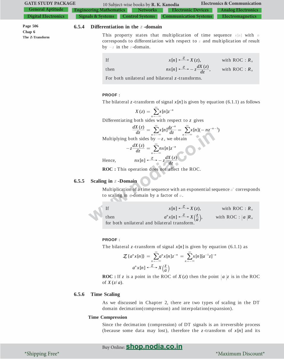
Page 506Chap 6The Z-Transform
www.nodia.co.in
GATE STUDY PACKAGE Electronics & Communication
Buy Online: shop.nodia.co.in *Shipping Free* *Maximum Discount*
Networks Electronic Devices Analog ElectronicsDigital Electronics Signals & Systems Control Systems ElectromagneticsCommunication SystemsGeneral Aptitude Engineering Mathematics
10 Subject-wise books by R. K. Kanodia
6.5.4 Differentiation in the z -domain
This property states that multiplication of time sequence [ ]x n with n corresponds to differentiation with respect to z and multiplication of result by z- in the z -domain.
If [ ]x n ( )X zZ , with ROC : Rx
then [ ]nx n ( )
z dzdX zZ - , with ROC : Rx
For both unilateral and bilateral z -transforms.
PROOF :
The bilateral z -transform of signal [ ]x n is given by equation (6.1.1) as follows
( )X z [ ]x n zn
n=3
3
=-
-/Differentiating both sides with respect to z gives
( )
dzdX z
[ ] [ ] ( )x n dzdz x n nz
n
nn
n
1= = -3
3
3
3
=-
-- -
=-/ /
Multiplying both sides by z- , we obtain
( )
z dzdX z- [ ]nx n z n
n
=3
3-
=-/
Hence, [ ]nx n ( )
z dzdX zZ -
ROC : This operation does not affect the ROC.
6.5.5 Scaling in z -Domain
Multiplication of a time sequence with an exponential sequence an corresponds to scaling in z -domain by a factor of a .
If [ ]x n ( )X zZ , with ROC : Rx
then [ ]a x nn X azZ
a k, with ROC : a Rx
for both unilateral and bilateral transform.
PROOF :
The bilateral z -transform of signal [ ]x n is given by equation (6.1.1) as
{ [ ]}a x nZ n [ ]a x n zn n
n
=3
3-
=-/ [ ] [ ]x n a z n
n
1=3
3- -
=-/
[ ]a x nn X azZ
a k
ROC : If z is a point in the ROC of ( )X z then the point a z is in the ROC of ( / )X z a .
6.5.6 Time Scaling
As we discussed in Chapter 2, there are two types of scaling in the DT domain decimation(compression) and interpolation(expansion).
Time Compression
Since the decimation (compression) of DT signals is an irreversible process (because some data may lost), therefore the z -transform of [ ]x n and its

Page 507Chap 6
The Z-Transform
www.nodia.co.in
Buy Online: shop.nodia.co.in *Shipping Free* *Maximum Discount*
GATE STUDY PACKAGE Electronics & Communication
Sample Chapter of Signals and Systems (Vol-7, GATE Study Package)
decimated sequence [ ] [ ]y n x an= not be related to each other.
Time Expansion
In the discrete time domain, time expansion of sequence [ ]x n is defined as
[ ]x nk [ / ] intif is a multiple of eger
otherwise
x n k n k
0= ) (6.5.1)
Time-scaling property of z -transform is derived only for time expansion which is given as
If [ ]x n ( )X zZ , with ROC : Rx
then [ ]x nk ( ) ( )X z X zkkZ = , with ROC : ( )R /
xk1
for both the unilateral and bilateral z -transform.
PROOF :The unilateral z -transform of expanded sequence [ ]x nk is given by
{ [ ]}x nZ k [ ]x n zkn
n 0
=3
-
=/
[0] [1] ... [ ]x x z x k zk k kk1= + + +- -
[ 1] ... [2 ] ...x k z x k z( )k
kk
k1 2+ + + +- + -
Since the expanded sequence [ ]x nk is zero everywhere except when n is a multiple of k . This reduces the above transform as follows
{ [ ]}x nZ k [0] [ ] [2 ] [3 ] ...x x k z x k z x k zk kk
kk
kk2 3= + + + +- - -
As defined in equation 6.5.1, interpolated sequence is
[ ]x nk [ / ]x n k=n 0= [ ]x 0k [ ]x 0= ,
n k= [ ]x kk [1]x=n k2= [ ]x k2k [ ]x 2=Thus, we can write
{ [ ]}x nZ k [0] [1] [2] [3] ...x x z x z x zk k k2 3= + + + +- - -
[ ] ( ) ( )x n z X zk n k
n 0
= =3
-
=/
NOTE :Time expansion of a DT sequence by a factor of k corresponds to replacing z as zk in its z-transform.
6.5.7 Time Differencing
If [ ]x n ( )X zZ , with ROC : Rx
then [ ] [ ]x n x n 1- - (1 ) ( )z X z1Z - - , with the ROC
: Rx except for the possible deletion of z 0= , for both unilateral and
bilateral transform.
PROOF :The z -transform of [ ] [ ]x n x n 1- - is given by equation (6.1.1) as follows
{ [ ] [ 1]}x n x nZ - - { [ ] [ ]}x n x n z1 n
n
= - -3
3-
=-/

Page 508Chap 6The Z-Transform
www.nodia.co.in
GATE STUDY PACKAGE Electronics & Communication
Buy Online: shop.nodia.co.in *Shipping Free* *Maximum Discount*
Networks Electronic Devices Analog ElectronicsDigital Electronics Signals & Systems Control Systems ElectromagneticsCommunication SystemsGeneral Aptitude Engineering Mathematics
10 Subject-wise books by R. K. Kanodia
[ ] [ ]x n z x n z1n
n
n
n
= - -3
3
3
3-
=-
-
=-/ /
In the second summation, substituting n r1- =
{ [ ] [ 1]}x n x nZ - - [ ] [ ]x n z x r z ( )n
n
r
r
1= -3
3
3
3-
=-
- +
=-/ /
[ ] [ ]x n z z x r zn
n
r
r
1= -3
3
3
3-
=-
- -
=-/ /
( ) ( )X z z X z1= - -
Hence, [ ] [ ]x n x n 1- - (1 ) ( )z X z1Z - -
6.5.8 Time Convolution
Time convolution property states that convolution of two sequence in time domain corresponds to multiplication in z -domain.
Let [ ]x n1 ( )X z1Z , ROC : R1
and [ ]x n2 ( )X z2Z , ROC : R2
then the convolution property states that
[ ] [ ]x n x n1 2* ( ) ( )X z X z1 2Z , ROC : at least R R1 2+
for both unilateral and bilateral z -transforms.
PROOF :As discussed in chapter 4, the convolution of two sequences is given by
[ ] [ ]x n x n1 2* [ ] [ ]x k x n kk
1 2= -3
3
=-/
Taking the z -transform of both sides gives
[ ] [ ]x n x n1 2* [ ] [ ]x k x n k z n
kn1 2
Z -3
3
3
3-
=-=-//
Interchanging the order of the two summations, we get
[ ] [ ]x n x n1 2* [ ] [ ]x k x n k zk n
n1 2
Z -3
3
3
3
=- =-
-/ /
Substituting n k a- = in the second summation
[ ] [ ]x n x n2* [ ] [ ]x k x z ( )
k
k1 2
Z a3
3
3
3a
a=-
- +
=-/ /
or [ ] [ ]x n x n2* [ ] [ ]x k z x zk
k1 2
Z a3
3
3
3a
a
-
=-
-
=-e eo o/ /
[ ] [ ]x n x n1 2* ( ) ( )X z X z1 2Z
6.5.9 Conjugation Property
If [ ]x n ( )X zZ , with ROC : Rx
then [ ]x n) ( )X zZ ) ) , with ROC : Rx
If [ ]x n is real, then ( )X z ( )X z= ) )

Page 509Chap 6
The Z-Transform
www.nodia.co.in
Buy Online: shop.nodia.co.in *Shipping Free* *Maximum Discount*
GATE STUDY PACKAGE Electronics & Communication
Sample Chapter of Signals and Systems (Vol-7, GATE Study Package)
PROOF :The z -transform of signal [ ]x n) is given by equation (6.1.1) as follows
{ [ ]}x nZ ) [ ]x n z n
n
= )
3
3-
=-/ [ ] ( )x n z n
n
= ) )
3
3-
=-6 @/ (6.5.2)
Let z -transform of [ ]x n is ( )X z
( )X z [ ]x n z n
n
=3
3-
=-/
by taking complex conjugate on both sides of above equation
( )X z) [ [ ] ]x n z n
n
= )
3
3-
=-/
Replacing z z" ), we will get
( )X z) ) [ ] ( )x n z n
n
= ))
3
3-
=-6 @/ (6.5.3)
Comparing equation (6.5.2) and (6.5.3)
{ [ ]}x nZ ) ( )X z= ) ) (6.5.4)
For real [ ]x n , [ ]x n) [ ]x n= , so
{ [ ]}x nZ ) [ ] ( )x n z X zn
n
= =3
3-
=-/ (6.5.5)
Comparing equation (6.5.4) and (6.5.5)
( )X z ( )X z= ) )
6.5.10 Initial Value Theorem
If [ ]x n ( )X zZ , with ROC : Rx
then initial-value theorem states that,
[ ]x 0 ( )limX zz
="3
The initial-value theorem is valid only for the unilateral Lapalce transform
PROOF :
For a causal signal [ ]x n
( )X z [ ]x n z n
n 0
=3
-
=/
[0] [1] [2] ...x x z x z1 2= + + +- -
Taking limit as z " 3 on both sides we get
( )limX zz"3
( [0] [1] [2] ...)lim x x z x zz
1 2= + + +"3
- - [ ]x 0= [ ]x 0 ( )limX z
z=
"3
6.5.11 Final Value Theorem
If [ ]x n ( )X zZ , with ROC : Rx
then final-value theorem states that
[ ]x 3 ( 1) ( )lim z X zz 1
= -"
Final value theorem is applicable if ( )X z has no poles outside the unit circle. This theorem can be applied to either the unilateral or bilateral z-transform.

Page 510Chap 6The Z-Transform
www.nodia.co.in
GATE STUDY PACKAGE Electronics & Communication
Buy Online: shop.nodia.co.in *Shipping Free* *Maximum Discount*
Networks Electronic Devices Analog ElectronicsDigital Electronics Signals & Systems Control Systems ElectromagneticsCommunication SystemsGeneral Aptitude Engineering Mathematics
10 Subject-wise books by R. K. Kanodia
PROOF :
{ [ 1]} { [ ]}x n x nZ Z+ - { [ ] [ ]}lim x n x n z1k
n
kn
0
= + -"3
=
-/
(6.5.6)
From the time shifting property of unilateral z -transform discussed in section 6.5.2
[ ]x n n0+ ( ) [ ]z X z x m zn m
m
n
0
1Z
0
0
- -
=
-
e o/
For n 10 = [ ]x n 1+ ( ) [ ]z X z x m z m
m 0
0Z - -
=e o/
[ ]x n 1+ ( ) [ ]z X z x 0Z -^ hPut above transformation in the equation (6.5.6)
[ ] [0] [ ]zX z zx X z- - ( [ ] [ ])lim x n x n z1k
n
n
k
0
= + -"3
-
=/
( 1) [ ] [0]z X z zx- - ( [ ] [ ])lim x n x n z1k
n
n
k
0
= + -"3
-
=/
Taking limit as z 1" on both sides we get
( 1) [ ] [0]lim z X z xz 1
- -"
[ ] [ ]lim x n x n1k
n
k
0
= + -"3
=/
( 1) [ ] [0]lim z X z xz 1
- -"
{( [1] [0]) ( [ ] [ ]) ( [ ] [ ]) ...lim x x x x x x2 1 3 2k
= - + - + - +"3
... ( [ ] [ ])x k x k1+ + - ( 1) [ ] [0]lim z X z xz 1
- -"
[ ] [ ]x x 03= -Hence, [ ]x 3 ( 1) ( )lim z X z
z 1= -
"
Summary of Properties
Let, [ ]x n ( )X zZ , with ROC Rx
[ ]x n1 ( )X z1Z , with ROC R1
[ ]x n2 ( )X z2Z , with ROC R2
The properties of z -transforms are summarized in the following table.
TABLE 6.2 Properties of z -transform
Properties Time domain z -transform ROC
Linearity [ ] [ ]ax n bx n1 2+ ( ) ( )aX z bX z1 2+ at least R R1 2+
Time shifting (bilateral or non-causal)
[ ]x n n0- ( )z X zn0- Rx except for the possible deletion or addition of
0 orz z 3= =[ ]x n n0+ ( )z X zn0
Time shifting (unilateral or causal)
[ ]x n n0-( )z X zn0-
^
[ ]x m zm
m
n
1
0
+ -=
o/ Rx except for the possible deletion or addition of
0 orz z 3= =[ ]x n n0+
( )z X zn0 ^
[ ]x m z m
m
n
0
10
- -
=
-
o/

Page 511Chap 6
The Z-Transform
www.nodia.co.in
Buy Online: shop.nodia.co.in *Shipping Free* *Maximum Discount*
GATE STUDY PACKAGE Electronics & Communication
Sample Chapter of Signals and Systems (Vol-7, GATE Study Package)
Properties Time domain z -transform ROC
Time reversal [ ]x n- X z1
b l /R1 x
Differentiation in z domain
[ ]nx n ( )z dzdX z- Rx
Scaling in z domain
[ ]a x nnX a
za k a Rx
Time scaling (expansion)
[ ] [ / ]x n x n kk = ( )X zk ( )R /x
k1
Time differencing
[ ] [ ]x n x n 1- - ( ) ( )z X z1 1- -Rx , except for the possible deletion of the origin
Time convolution
[ ] [ ]x n x n1 2* ( ) ( )X z X z1 2 at least R R1 2+
Conjugations [ ]x n) ( )X z) ) Rx
Initial-value theorem
[ ] ( )limx X z0z
="3
provided [ ]x n 0= for n 0<
Final-value theorem
[ ]
[ ]
( ) ( )
lim
lim
x
x n
z X z1n
z 1
3
=
= -"
"
3provided [ ]x 3 exists
6.6 ANALYSIS OF DISCRETE LTI SYSTEMS USING z-TRANSFORM
The z -transform is very useful tool in the analysis of discrete LTI system. As the Laplace transform is used in solving differential equations which describe continuous LTI systems, the z -transform is used to solve difference equation which describe the discrete LTI systems.
Similar to Laplace transform, for CT domain, the z -transform gives transfer function of the LTI discrete systems which is the ratio of the z-transform of the output variable to the z -transform of the input variable.These applications are discussed as follows
6.6.1 Response of LTI Continuous Time System
As discussed in chapter 4 (section 4.8), a discrete-time LTI system is always described by a linear constant coefficient difference equation given as follows
[ ]a y n kkk
N
0
-=/ [ ]b x n kk
k
M
0
= -=/
[ ] [ ( 1)] ....... [ 1] [ ]a y n N a y n N a y n a y nN N 1 1 0- + - - + + - +-
[ ] [ ( 1)] ..... [ 1] [ ]b x n M b x n M b x n b x nM M 1 1 0= - + - - + + - +- (6.6.1)where, N is order of the system.
The time-shift property of z -transform [ ] ( )x n n z X zn0
Z0- - , is used
to solve the above difference equation which converts it into an algebraic equation. By taking z -transform of above equation
Page 512Chap 6The Z-Transform
www.nodia.co.in
GATE STUDY PACKAGE Electronics & Communication
Buy Online: shop.nodia.co.in *Shipping Free* *Maximum Discount*
Networks Electronic Devices Analog ElectronicsDigital Electronics Signals & Systems Control Systems ElectromagneticsCommunication SystemsGeneral Aptitude Engineering Mathematics
10 Subject-wise books by R. K. Kanodia
( ) ( )] ....... ( )a z Y z a z Y z a z a Y z( )N
NN
N1
11
10+ + + +-
-- - -
( ) ( ) ..... ( ) ( )b z X z b z X z b z X x b X z( )M
MM
M1
11
10= + + + +-
-- - -
( )( )
X zY z
..........
a z a z a ab z b z b b
NN
NN
MN
MM
11
1 0
11
1 0=+ + + ++ + + +
--
--
-
this equation can be solved for ( )Y z to find the response [ ]y n .The solution or total response [ ]y n consists of two parts as discussed below.
1. Zero-input Response or Free Response or Natural Response
The zero input response [ ]y nzi is mainly due to initial output in the system. The zero-input response is obtained from system equation (6.6.1) when input [ ] 0x n = .
By substituting [ ] 0x n = and [ ] [ ]y n y nzi= in equation (6.6.1), we get
[ ] [ ( 1)] ....... [ 1] [ ]a y n N a y n N a y n a y nN N 1 1 0- + - - + + - +- 0=On taking z -transform of the above equation with given initial conditions,
we can form an equation for ( )Y zzi . The zero-input response [ ]y nzi is given by inverse z -transform of ( )Y zzi .
NOTE :The zero input response is also called the natural response of the system and it is denoted as [ ]y nN .
2. Zero-State Response or Forced Response
The zero-state response [ ]y nzs is the response of the system due to input signal and with zero initial conditions. The zero-state response is obtained from the difference equation (6.6.1) governing the system for specific input signal [ ]x n for 0n $ and with zero initial conditions.Substituting [ ] [ ]y n y nzs= in equation (6.6.1) we get,
[ ] [ ( 1)] ....... [ 1] [ ]a y n N a y n N a y n a y nN zs N zs zs zs1 1 0- + - - + + - +-
[ ] [ ( 1)] ..... [ 1] [ ]b x n M b x n M b x n b x nM M 1 1 0= - + - - + + - +-
Taking z -transform of the above equation with zero initial conditions for output (i.e., [ ] [ ] ...y y1 2 0- = - = we can form an equation for ( )Y zzs .
The zero-state response [ ]y nzs is given by inverse z -transform of ( )Y zzs .
NOTE :The zero state response is also called the forced response of the system and it is denoted as
[ ]y nF .
Total Response
The total response [ ]y n is the response of the system due to input signal and initial output. The total response can be obtained in following two ways :
Taking z -transform of equation (6.6.1) with non-zero initial conditions for both input and output, and then substituting for ( )X z we can form an equation for ( )Y z . The total response [ ]y n is given by inverse Laplace transform of ( )Y s .
Alternatively, that total response [ ]y n is given by sum of zero-input response [ ]y nzi and zero-state response [ ]y nzs .Therefore total response,
[ ]y n [ ] [ ]y n y nzi zs= +
6.6.2 Impulse Response and Transfer Function
System function or transfer function is defined as the ratio of the z -transform of the output [ ]y n and the input [ ]x n with zero initial conditions.Let [ ] ( )x n X zZ is the input and [ ] ( )y n Y zL is the output of an LTI discrete time system having impulse response ( ) ( )h n H zL . The response

Page 513Chap 6
The Z-Transform
www.nodia.co.in
Buy Online: shop.nodia.co.in *Shipping Free* *Maximum Discount*
GATE STUDY PACKAGE Electronics & Communication
Sample Chapter of Signals and Systems (Vol-7, GATE Study Package)
[ ]y n of the discrete time system is given by convolution sum of input and impulse response as
[ ]y n [ ] [ ]x n h n= *By applying convolution property of z -transform we obtain
( )Y z ( ) ( )X z H z=
( )H z ( )( )
X zY z=
where, ( )H z is defined as the transfer function of the system. It is the z-transform of the impulse response.
Alternatively we can say that the inverse z -transform of transfer function is the impulse response of the system.Impulse response
[ ]h n { ( )}( )( )
H zX zY z
Z Z1 1= =- -) 3
6.7 STABILITY AND CAUSALITY OF LTI DISCRETE SYSTEMS USING z-TRANSFORM
z -transform is also used in characterization of LTI discrete systems. In this section, we derive a z -domain condition to check the stability and causality of a system directly from its z -transfer function.
6.7.1 Causality
A linear time-invariant discrete time system is said to be causal if the impulse response [ ]h n 0= , for n 0< and it is therefore right-sided. The ROC of such a system ( )H z is the exterior of a circle. If ( )H z is rational then the system is said to be causal if
1. The ROC is the exterior of a circle outside the outermost pole ; and
2. The degree of the numerator polynomial of ( )H z should be less than or equal to the degree of the denominator polynomial.
6.7.2 Stability
An LTI discrete-time system is said to be BIBO stable if the impulse response [ ]h n is summable. That is
[ ]h nn 3
3
=-/ < 3
z -transform of [ ]h n is given as
( )H z [ ]h n z n
n
=3
3-
=-/
Let z ej= W(which describes a unit circle in the z -plane), then
[ ]H ejW [ ]h n e j n
n
=3
3W-
=-/
[ ]h n e j n
n
#3
3W-
=-/
[ ]h n <n
3=3
3
=-/
which is the condition for the stability. Thus we can conclude that

Page 514Chap 6The Z-Transform
www.nodia.co.in
GATE STUDY PACKAGE Electronics & Communication
Buy Online: shop.nodia.co.in *Shipping Free* *Maximum Discount*
Networks Electronic Devices Analog ElectronicsDigital Electronics Signals & Systems Control Systems ElectromagneticsCommunication SystemsGeneral Aptitude Engineering Mathematics
10 Subject-wise books by R. K. Kanodia
STABILITY OF LTI DISCRETE SYSTEM
An LTI system is stable if the ROC of its system function ( )H z contains the unit circle z 1=
6.7.3 Stability and Causality
As we discussed previously, for a causal system with rational transfer function ( )H z , the ROC is outside the outermost pole. For the BIBO stability the
ROC should include the unit circle z 1= . Thus, for the system to be causal and stable theses two conditions are satisfied if all the poles are within the unit circle in the z -plane.
STABILITY AND CAUSALITY OF LTI DISCRETE SYSTEM
An LTI discrete time system with the rational system function ( )H z is said to be both causal and stable if all the poles of ( )H z lies inside the unit circle.
6.8 BLOCK DIAGRAM REPRESENTATION
In z -domain, the input-output relation of an LTI discrete time system is represented by the transfer function ( )H z ,which is a rational function of z , as shown in equation
( )H z ( )( )
X zY z=
......
a z a z a z a z ab z b z b z b z b
N N NN N
M M MM M
0 11
22
1
0 11
22
1=+ + + + ++ + + + +
- --
- --
where, N = Order of the system, M N# and a 10 =The above transfer function is realized using unit delay elements, unit
advance elements, adders and multipliers. Basic elements of block diagram with their z -domain representation is shown in table 6.3.
TABLE 6.3 : Basic Elements of Block Diagram
Elements of Block diagram
Time Domain Representation s -domain Representation
Adder
Constant multiplier
Unit delay element
Unit advance element

Page 515Chap 6
The Z-Transform
www.nodia.co.in
Buy Online: shop.nodia.co.in *Shipping Free* *Maximum Discount*
GATE STUDY PACKAGE Electronics & Communication
Sample Chapter of Signals and Systems (Vol-7, GATE Study Package)
The different types of structures for realizing discrete time systems are same as we discussed for the continuous-time system in the previous chapter.
6.8.1 Direct Form I Realization
Consider the difference equation governing the discrete time system with a 10 = ,
[ ] [ 1] [ 2] .... [ ]y n a y n a y n a y n NN1 2+ - + - + + - [ ] [ 1] [ 2] ... [ ]b x n b x n b x n b x n MM0 1 2= + - + - + + -Taking Z transform of the above equation we get,
( )Y z ( ) ( ) ... ( )a z Y z a z Y z a z Y zNN
11
22=- - - - +- - -
( ) ( ) ( ) ... ( )b X z b z X z b z X z b z X zMM
0 11
22+ + + +- - - (6.8.1)
The above equation of ( )Y z can be directly represented by a block diagram as shown in figure 6.8.1a. This structure is called direct form-I structure. This structure uses separate delay elements for both input and output of the system. So, this realization uses more memory.
Figure 6.8.1a General structure of direct form-realization
For example consider a discrete LTI system which has the following impulse response
( )H z ( )( )
X zY z
z zz z
1 4 31 2 2
1 2
1 2
= =+ ++ +
- -
- -
( ) ( ) 3 ( ) 1 ( ) 2 ( ) ( )Y z z Y z z Y z X z z X z z X z4 21 2 1 2+ + = + +- - - -
Comparing with standard form of equation (6.8.1), we get a 41 = , a 32 = and b 10 = , b 21 = , b 22 = . Now put these values in general structure of Direct form-I realization we get

Page 516Chap 6The Z-Transform
www.nodia.co.in
GATE STUDY PACKAGE Electronics & Communication
Buy Online: shop.nodia.co.in *Shipping Free* *Maximum Discount*
Networks Electronic Devices Analog ElectronicsDigital Electronics Signals & Systems Control Systems ElectromagneticsCommunication SystemsGeneral Aptitude Engineering Mathematics
10 Subject-wise books by R. K. Kanodia
Figure 6.8.1b
6.8.2 Direct Form II Realization
Consider the general difference equation governing a discrete LTI system
[ ] [ 1] [ 2] .... [ ]y n a y n a y n a y n NN1 2+ - + - + + - [ ] [ 1] [ 2] ... [ ]b x n b x n b x n b x n MM0 1 2= + - + - + + -Taking Z transform of the above equation we get,
( )Y z ( ) ( ) ... ( )a z Y z a z Y z a z Y zNN
11
22=- - - - +- - -
( ) ( ) ( ) ... ( )b X z b z X z b z X z b z X zMM
0 11
22+ + + +- - -
It can be simplified as,( ) ... ( ) ...Y z a z a z a z X z b b z b z b z1 N
NM
M1
12
20 1
12
2+ + + + = + + + +- - - - - -6 6@ @
Let, ( )( )
X zY z
( )( )
( )( )
X zW z
W zY z
#=where,
( )( )
X zW z
...a z a z a z1
1N
N1
12
2=+ + + +- - - (6.8.2)
( )( )
W zY z
...b b z b z b zMM
0 11
22= + + + +- - - (6.8.3)
Equation (6.8.2) can be simplified as,( ) ( ) ( ) ... ( ) ( )W z a z W z a z W z a z W z X zN
N1
12
2+ + + + =- - -
( ) ( ) ( ) ( ) ... ( )W z X z a z W z a z W z a z W zNN
11
22= - - - -- - - (6.8.4)
Similarly by simplifying equation (6.8.3), we get
( ) ( ) ( ) ( ) ... ( )Y z b W z b z W z b z W z b z W zMM
0 11
22= + + + +- - - (6.8.5)
Equation (6.8.4) and (6.8.5) can be realized together by a direct structure called direct form-II structure as shown in figure 6.8.2a. It uses less number of delay elements then the Direct Form I structure.
For example, consider the same transfer function ( )H z which is discussed above
( )H z ( )( )
X zY z
z zz z
1 4 31 2 2
1 2
1 2
= =+ ++ +
- -
- -
Let ( )( )
X zY z
( )( )
( )( )
W zY z
X zW z
#=
where, ( )( )
X zW z
z z1 4 3
11 2=
+ +- - ,
( )( )
W zY z
z z1 2 21 2= + +- -
so, ( )W z ( ) ( ) ( )X z z W z z W z4 31 2= - -- -
and ( )Y z ( ) ( ) ( )W z z W z z W z1 2 21 2= + +- -
Comparing these equations with standard form of equation (6.8.4) and (6.8.5), we have a 41 = , a 32 = and , ,b b b1 2 20 1 2= = = . Substitute these

Page 517Chap 6
The Z-Transform
www.nodia.co.in
Buy Online: shop.nodia.co.in *Shipping Free* *Maximum Discount*
GATE STUDY PACKAGE Electronics & Communication
Sample Chapter of Signals and Systems (Vol-7, GATE Study Package)
values in general structure of Direct form II , we get as shown in figure 6.8.2b
Figure 6.8.2a General structure of direct form-II realization
Figure 6.8.2b
6.8.3 Cascade Form
The transfer function ( )H z of a discrete time system can be expressed as a product of several transfer functions. Each of these transfer functions is realized in direct form-I or direct form II realization and then they are cascaded.Consider a system with transfer function
( )H z ( )( )
( )( )a z a z a z a z
b b z b z b b z b z1 1k k m m
k k k m m m
11
22
11
22
0 11
22
0 11
22
=+ + + ++ + + +
- - - -
- - - -
( ) ( )H z H z1 2=
where ( )H z1 a z a z
b b z b z1 k k
k k k
11
22
0 11
22
=+ ++ +
- -
- -

Page 518Chap 6The Z-Transform
www.nodia.co.in
GATE STUDY PACKAGE Electronics & Communication
Buy Online: shop.nodia.co.in *Shipping Free* *Maximum Discount*
Networks Electronic Devices Analog ElectronicsDigital Electronics Signals & Systems Control Systems ElectromagneticsCommunication SystemsGeneral Aptitude Engineering Mathematics
10 Subject-wise books by R. K. Kanodia
( )H z2 a z a z
b b z b z1 m m
m m m
11
22
0 11
22
=+ ++ +
- -
- -
Realizing ( ) ( )andH z H z1 2 in direct form II and cascading we obtain cascade form of the system function ( )H z as shown in figure 6.8.3.
Figure 6.8.3 Cascaded form realization of discrete LTI system
6.8.4 Parallel Form
The transfer function ( )H z of a discrete time system can be expressed as the sum of several transfer functions using partial fractions. Then the individual transfer functions are realized in direct form I or direct form II realization and connected in parallel for the realization of ( )H z . Let us consider the transfer function
( )H z ......cp zc
p zc
p zc
1 1 1z n
N
11
11
21= +
-+
-+
-- - -
Now each factor in the system is realized in direct form II and connected in parallel as shown in figure 6.8.4.
Figure 6.8.4 Parallel form realization of discrete LTI system
6.9 RELATIONSHIP BETWEEN s-PLANE & �-PLANE
There exists a close relationship between the Laplace and z -transforms. We

Page 519Chap 6
The Z-Transform
www.nodia.co.in
Buy Online: shop.nodia.co.in *Shipping Free* *Maximum Discount*
GATE STUDY PACKAGE Electronics & Communication
Sample Chapter of Signals and Systems (Vol-7, GATE Study Package)
know that a DT sequence [ ]x n is obtained by sampling a CT signal ( )x t with a sampling interval T , the CT sampled signal ( )x ts is written as follows
( )x ts ( ) ( )x nT t nTn
d= -3
3
=-/
where ( )x nT are sampled value of ( )x t which equals the DT sequence [ ]x n . Taking the Laplace transform of ( )x ts , we have
( ) { ( )}X s L x ts= ( ) { ( )}x nT L t nTn
d= -3
3
=-/
( )X nT e nTs
n
=3
3-
=-/ (6.9.1)
The z -transform of [ ]x n is given by
( )X z [ ]x n z n
n
=3
3-
=-/ (6.9.2)
Comparing equation (6.9.1) and (6.9.2)
( )X s ( )X zz esT
==
[ ] ( )x n x nT=
***********

Page 520Chap 6The Z-Transform
www.nodia.co.in
GATE STUDY PACKAGE Electronics & Communication
Buy Online: shop.nodia.co.in *Shipping Free* *Maximum Discount*
Networks Electronic Devices Analog ElectronicsDigital Electronics Signals & Systems Control Systems ElectromagneticsCommunication SystemsGeneral Aptitude Engineering Mathematics
10 Subject-wise books by R. K. Kanodia
EXERCISE 6.1
MCQ 6.1.1 The z -transform and its ROC of a discrete time sequence
[ ]x n , 0
,
n
n21
0 0
<n
$
=-b l*
will be
(A) ,zz z2 1
221>- (B) ,z
z z2 21<-
(C) ,zz z2 1
221<- (D) ,z
z z12
21>
1
--
MCQ 6.1.2 The ROC of z -transform of the discrete time sequence [ ]x n | |n21= ^ h is
(A) 2z< <21 (B) z 2>
(C) z2 2< <- (D) z < 21
MCQ 6.1.3 Consider a discrete-time signal [ ]x n [ ] [ 1]u n u n31
21n n
= + - -b bl l . The ROC of its z -transform is
(A) z3 2< < (B) z 21<
(C) z 31> (D) z3
121< <
MCQ 6.1.4 For a signal [ ] [ ] [ ]x n u nn na a= + - , the ROC of its z -transform would be
(A) ,minz 1> a ae o (B) z > a
(C) ,maxz 1> a ae o (D) z < a
MCQ 6.1.5 Match List I (discrete time sequence) with List II (z -transform) and choose the correct answer using the codes given below the lists:
List-I (Discrete Time Sequence) List-II (z -Transform)
P. [ 2]u n - 1.( )
, 1z z
z11 <2 1-- -
Q. [ 3]u n- - - 2. , 1z
z z1
<1
1
--
-
-
R. [ 4]u n + 3.( )
, 1z z
z11 >4 1-- -
S. [ ]u n- 4. ,z
z z1
1>1
2
- -
-
Codes : P Q R S(A) 1 4 2 3(B) 2 4 1 3(C) 4 1 3 2(D) 4 2 3 1

Page 521Chap 6
The Z-Transform
www.nodia.co.in
Buy Online: shop.nodia.co.in *Shipping Free* *Maximum Discount*
GATE STUDY PACKAGE Electronics & Communication
Sample Chapter of Signals and Systems (Vol-7, GATE Study Package)
MCQ 6.1.6 The z -transform of signal [ ] [ ]x n e u njn= p is
(A) , : 1ROCzz z1 >+ (B) , : 1ROCz j
z z >-
(C) , : 1ROCz
z z1
<2 + (D) , : 1ROCz z1
1 <+
MCQ 6.1.7 Consider the pole zero diagram of an LTI system shown in the figure which corresponds to transfer function ( )H z .
Match List I (The impulse response) with List II (ROC which corresponds to above diagram) and choose the correct answer using the codes given below:{Given that ( )H 1 1= }
List-I (Impulse Response) List-II (ROC)
P. [( 4)2 6(3) ] [ ]u nn n- + 1. does not exist
Q. ( ) [ ] ( ) [ ]u n u n4 2 6 3 1n n- + - - - 2. z 3>
R. ( ) [ ] ( ) [ ]u n u n4 2 1 6 3 1n n- - + - - - 3. z 2<
S. ( ) [ ] ( ) [ ]u n u n4 2 1 6 3n n- - + - 4. z2 3< <
Codes : P Q R S(A) 4 1 3 2(B) 2 1 3 4(C) 1 4 2 3(D) 2 4 3 1
MCQ 6.1.8 The z -transform of a signal [ ]x n is ( )X z e e /z z1= + , z 0! . [ ]x n would be
(A) [ ] !n n1d + (B) [ ] !u n n
1+
(C) [ 1] !u n n- + (D) [ ] ( ) !n n 1d + -
Common Data For Q. 9 to 11:Consider a discrete time signal [ ]x n and its z -transform ( )X z given as
( )X z z z
z z2 3
52
2
=- -+
MCQ 6.1.9 If ROC of ( )X z is z 1< , then signal [ ]x n would be
(A) [ 2(3) ( 1) ] [ ]u n 1n n- + - - - (B) [2(3) ( 1) ] [ ]u nn n- -(C) ( ) [ ] ( ) [ ]u n u n2 3 1 1n n- - - - - (D) [ ( ) ] [ ]u n2 3 1n +
MCQ 6.1.10 If ROC of ( )X z is z 3> , then signal [ ]x n would be(A) [ ( ) ( ) [ ]u n2 3 1n n- - (B) [ ( ) ( ) ] [ ]u n2 3 1 1n n- + - - -(C) ( ) [ ] ( ) [ ]u n u n2 3 1 1n n- - - - - (D) [ ( ) ] [ ]u n2 3 1n +

Page 522Chap 6The Z-Transform
www.nodia.co.in
GATE STUDY PACKAGE Electronics & Communication
Buy Online: shop.nodia.co.in *Shipping Free* *Maximum Discount*
Networks Electronic Devices Analog ElectronicsDigital Electronics Signals & Systems Control Systems ElectromagneticsCommunication SystemsGeneral Aptitude Engineering Mathematics
10 Subject-wise books by R. K. Kanodia
MCQ 6.1.11 If ROC of ( )X z is z1 3< < , the signal [ ]x n would be(A) [ ( ) ( ) ] [ ]u n2 3 1n n- - (B) [ ( ) ( ) ] [ ]u n2 3 1 1n n- + - - -(C) ( ) [ ] ( ) [ ]u n u n2 3 1 1n n- - - - - (D) [ ( ) ( ) ] [ ]u n2 3 1 1n n+ - - -
MCQ 6.1.12 Consider a DT sequence [ ]x n [ ] [ ]x n x n1 2= + where, [ ]x n1 ( . ) [ ]u n0 7 1n= - and [ ] ( 0.4) [ 2]x n u nn
2 = - - . The region of convergence of z -transform of [ ]x n is(A) . .z0 4 0 7< < (B) .z 0 7>(C) .z 0 4< (D) none of these
MCQ 6.1.13 The z -transform of a DT signal [ ]x n is ( )X z z z
z8 2 12=
- -. What will be the
z -transform of [ ]x n 4- ?
(A) ( ) ( )
( )z z
z8 4 2 4 1
42+ - + -
+ (B)
z zz
8 2 12
5
- -
(C) z z
z128 8 1
42 - -
(D) z z z8 2
15 4 3- -
MCQ 6.1.14 Let [ ], [ ]x n x n1 2 and [ ]x n3 be three discrete time signals and ( ), ( )X z X z1 2 and ( )X z3 are their z -transform respectively given as
( )X z1 ( )( . )z z
z1 0 5
2
= - - ,
( )X z2 ( )( . )z z
z1 0 5
= - -
and ( )X z3 ( )( . )z z1 0 5
1= - -Then [ ], [ ]x n x n1 2 and [ ]x n3 are related as(A) [ ] [ ] [ ]x n x n x n2 11 2 3- = - = (B) [ ] [ ] [ ]x n x n x n2 11 2 3+ = + =(C) [ ] [ ] [ ]x n x n x n1 21 2 3= - = - (D) [ ] [ ] [ ]x n x n x n1 11 2 3+ = - =
MCQ 6.1.15 The z -transform of the discrete time signal [ ]x n shown in the figure is
(A) z
z1
k
1- -
- (B)
zz
1
k
1+ -
-
(C) zz
11 k
1--
-
- (D)
zz
11 k
1-+
-
-
MCQ 6.1.16 Consider the unilateral z -transform pair [ ] ( )x n X z zz
1Z = - . The z
-transform of [ ]x n 1- and [ ]x n 1+ are respectively
(A) zz
12
- , z 11- (B) z 1
1- , z
z1
2
-
(C) z 11- , z
z1- (D) z
z1- , z
z1
2
-
MCQ 6.1.17 A discrete time causal signal [ ]x n has the z -transform
( )X z . , : 0.4ROCzz z0 4 >= -
The ROC for z -transform of the even part of [ ]x n will be

Page 523Chap 6
The Z-Transform
www.nodia.co.in
Buy Online: shop.nodia.co.in *Shipping Free* *Maximum Discount*
GATE STUDY PACKAGE Electronics & Communication
Sample Chapter of Signals and Systems (Vol-7, GATE Study Package)
(A) same as ROC of ( )X z (B) . .z0 4 2 5< <(C) .z 0 2> (D) .z 0 8>
MCQ 6.1.18 Match List I (Discrete time sequence) with List II (z -transform) and select the correct answer using the codes given below the lists.
List-I (Discrete time sequence) List-II (z -transform)
P. ( ) [ ]n u n1 n- 1.( )
, :ROCz
z z1
1>1 2
1
- -
-
Q. [ ]nu n 1- - - 2.( )
, : 1ROCz
z1
1 >1+ -
R. ( ) [ ]u n1 n- 3.( )
, : 1ROCz
z z1
<1 2
1
- -
-
S. [ ]nu n 4.( )
, : 1ROCz
z z1
>1 2
1
-+ -
-
Codes : P Q R S(A) 4 1 2 3(B) 4 3 2 1(C) 3 1 4 2(D) 2 4 1 3
MCQ 6.1.19 A discrete time sequence is defined as [ ]x n ( 2) [ 1]u nnn1= - - -- . The z
-transform of [ ]x n is
(A) , :log ROCz z21
21<+b l (B) , :log ROCz z2
121<-b l
(C) ( 2), : 2log ROCz z >- (D) ( 2), : 2log ROCz z <+
MCQ 6.1.20 Consider a z -transform pair [ ] ( )x n X zZ with ROC Rx . The z transform and its ROC for [ ] [ ]y n a x nn= will be
(A) , :ROCX az a Rxa k (B) ( ), :ROCX z a Rx+
(C) ( ), :ROCz X z Rax
- (D) ( ), :ROCX az a Rx
MCQ 6.1.21 Let ( )X z be the z -transform of a causal signal [ ] [ ]x n a u nn= with :ROC z a> . Match the discrete sequences , ,S S S1 2 3 and S4 with ROC of their z -transforms
,R R1 2 and R3.
Sequences ROC
:S1 [ ]x n 2- :R1 z a>
:S2 [ ]x n 2+ :R2 z a<
:S3 [ ]x n- :R3 z a1<
:S4 ( ) [ ]x n1 n-
(A) ( , ),( , ),( , ),( , )S R S R S R S R1 1 2 2 3 3 4 3
(B) ( , ),( , ),( , ),( , )S R S R S R S R1 1 2 1 3 3 4 1
(C) ( , ),( , ),( , ),( , )S R S R S R S R1 2 2 1 3 2 4 3
(D) ( , ),( , ),( , ),( , )S R S R S R S R1 1 2 2 3 2 4 3

Page 524Chap 6The Z-Transform
www.nodia.co.in
GATE STUDY PACKAGE Electronics & Communication
Buy Online: shop.nodia.co.in *Shipping Free* *Maximum Discount*
Networks Electronic Devices Analog ElectronicsDigital Electronics Signals & Systems Control Systems ElectromagneticsCommunication SystemsGeneral Aptitude Engineering Mathematics
10 Subject-wise books by R. K. Kanodia
MCQ 6.1.22 Consider a discrete time signal [ ] [ ]x n u nna= and its z -transform ( )X z . Match List I (discrete signals) with List II (z -transform) and select the correct answer using the codes given below:
List-I (Discrete time signal) List-II (z -transform)
P. [ / ]x n 2 1. ( )z X z2-
Q. [ ] [ ]x n u n2 2- - 2. ( )X z2
R. [ ] [ ]x n u n2+ 3. ( / )X z 2b
S. [ ]x nn2b 4. ( )X z2a
Codes : P Q R S(A) 1 2 4 3(B) 2 4 1 3(C) 1 4 2 3(D) 2 1 4 3
MCQ 6.1.23 The z -transform of a discrete sequence [ ]x n is ( )X z , then the z -transform of [ ]x n2 will be
(A) ( )X z2 (B) X z2a k
(C) ( ) ( )X z X z21 + -8 B (D) ( )X z
MCQ 6.1.24 Consider a signal [ ]x n and its z transform ( )X z given as
( )X z z z
z8 2 1
42=- -
The z -transform of the sequence [ ]y n [0] [1] [2] ..... [ ]x x x x n= + + + + will be
(A) ( )( )z z z
z1 8 2 1
42
2
- - - (B)
( )z zz z
8 2 14 12 - -
-
(C) ( )( )z z z
z1 8 2 1
42
2
+ - - (D)
( )z zz z
8 2 14 12 - -
+
MCQ 6.1.25 What is the convolution of two DT sequence [ ] { ,2,0,3}x n 1= --
and [ ] {2,0, }h n 3=
-
(A) { 2, 4, , 6, 9}3- --
(B) { 2, 4, , 12, 0, 9}3- --
(C) {9, 6, , 4, 2}3 - --
(D) { , 6, 7, 4, 6}3--
MCQ 6.1.26 If [ ] ( )x n X zZ be a z -transform pair, then which of the following is true?
(A) [ ] ( )x n X zZ -) ) (B) [ ] ( )x n X zZ -) )
(C) [ ] ( )x n X zZ) ) ) (D) [ ] ( )x n X zZ -) ) )
MCQ 6.1.27 A discrete-time system with input [ ]x n and output [ ]y n is governed by following difference equation
[ ] [ ]y n y n21 1- - [ ]x n= , with initial condition [ ]y 1 3- =
The impulse response of the system
(A) 1 , 0n n25
2 $-a k (B) , 0n25
21 n
$b l
(C) , 0n25
21 n 1
$-
b l (D) , 0n25
21 n 1
$+
b l

Page 525Chap 6
The Z-Transform
www.nodia.co.in
Buy Online: shop.nodia.co.in *Shipping Free* *Maximum Discount*
GATE STUDY PACKAGE Electronics & Communication
Sample Chapter of Signals and Systems (Vol-7, GATE Study Package)
MCQ 6.1.28 Consider a causal system with impulse response [ ] ( ) [ ]h n u n2 n= . If [ ]x n is the input and [ ]y n is the output to this system, then which of the following difference equation describes the system ?(A) [ ] [ ] [ ]y n y n x n2 1+ + = (B) [ ] [ ] [ ]y n y n x n2 1- - =
(C) [ ] [ ] [ ]y n y n x n2 1+ - = (D) [ ] [ ] [ ]y n y n x n21 1- - =
MCQ 6.1.29 The impulse response of a system is given as [ ]h n [ ] ( ) [ ]n u nn21d= - - . For an
input [ ]x n and output [ ]y n , the difference equation that describes the system is(A) [ ] [ ] [ ]y n y n x n2 1 2+ - = (B) [ ] . [ ] . [ ]y n y n x n0 5 1 0 5 1+ - = -(C) [ ] [ ] [ ]y n ny n x n2 1+ - = (D) [ ] 0.5 [ ] . [ ]y n y n x n1 0 5 1- - = -
MCQ 6.1.30 The input-output relationship of a system is given as [ ] 0.4 [ 1] [ ]y n y n x n- - = where, [ ]x n and [ ]y n are the input and output respectively. The zero state response of the system for an input [ ] ( . ) [ ]x n u n0 4 n= is(A) ( . ) [ ]n u n0 4 n (B) ( . ) [ ]n u n0 4 n2
(C) ( )( . ) [ ]n u n1 0 4 n+ (D) ( . ) [ ]n u n1 0 4 n
MCQ 6.1.31 A discrete time system has the following input-output relationship [ ] [ 1] [ ]y n y n x n2
1- - = . If an input [ ] [ ]x n u n= is applied to the system, then its zero state response will be
(A) ( ) [ ]u n21 2 n-: D (B) [ ]u n2 2
1 n- b l; E
(C) [ ]u n21
21 n
- b l; E (D) [ ( ) ] [ ]u n2 2 n-
MCQ 6.1.32 Consider the transfer function of a system
( )H z ( )
z zz z
4 42 12=+ +
-
For an input [ ] [ ] [ ]x n n n2 1d d= + + , the system output is(A) [ ] ( ) [ ]n u n2 1 6 2 nd + + (B) [ ] ( ) [ ]n u n2 6 2 nd - -
(C) [ ] ( ) [ ]n u n2 1 6 2 nd + - - (D) [ ] [ ]n u n2 1 6 21 n
d + + b l
MCQ 6.1.33 The transfer function of a discrete time LTI system is given as
( )H z , : 1ROCz
z z1
>2=+
Consider the following statements1. The system is causal and BIBO stable.
2. The system is causal but BIBO unstable.
3. The system is non-causal and BIBO unstable.
4. Impulse response [ ] [ ]sinh n n u n2p= a k
Which of the above statements are true ?(A) 1 and 4 (B) 2 and 4
(C) 1 only (D) 3 and 4
MCQ 6.1.34 Which of the following statement is not true?An LTI system with rational transfer function ( )H z is(A) causal if the ROC is the exterior of a circle outside the outermost pole.
(B) stable if the ROC of ( )H z includes the unit circle z 1= .
(C) causal and stable if all the poles of ( )H z lie inside unit circle.
(D) none of above

Page 526Chap 6The Z-Transform
www.nodia.co.in
GATE STUDY PACKAGE Electronics & Communication
Buy Online: shop.nodia.co.in *Shipping Free* *Maximum Discount*
Networks Electronic Devices Analog ElectronicsDigital Electronics Signals & Systems Control Systems ElectromagneticsCommunication SystemsGeneral Aptitude Engineering Mathematics
10 Subject-wise books by R. K. Kanodia
MCQ 6.1.35 If [ ]h n denotes the impulse response of a causal system, then which of the following system is not stable?
(A) [ ] [ ]h n n u n31 n
= b l (B) [ ] [ ]h n n31 d=
(C) [ ] [ ] [ ]h n n u n31 n
d= - -b l (D) [ ] [( ) ( ) ] [ ]h n u n2 3n n= -
MCQ 6.1.36 A causal system with input [ ]x n and output [ ]y n has the following relationship
[ ] [ ] [ ]y n y n y n3 1 2 2+ - + - [ ] [ ]x n x n2 3 1= + -The system is(A) stable (B) unstable
(C) marginally stable (D) none of these
MCQ 6.1.37 A causal LTI system is described by the difference equation [ ]y n [ ] [ ]x n y n 1= + -
Consider the following statement1. Impulse response of the system is [ ] [ ]h n u n=2. The system is BIBO stable
3. For an input [ ] ( . ) [ ]x n u n0 5 n= , system output is [ ] [ ] ( . ) [ ]y n u n u n2 0 5 n= -Which of the above statements is/are true?(A) 1 and 2 (B) 1 and 3
(C) 2 and 3 (D) 1, 2 and 3
MCQ 6.1.38 Match List I (system transfer function) with List II (property of system) and choose the correct answer using the codes given below
List-I (System transfer function) List-II (Property of system)
P. ( )( . )
, : 1.2ROCH zz
z z1 2
>3
3
=-
1. Non causal but stable
Q. ( )( . )
, : 1.2ROCH zz
z z1 2
<3
2
=-
2. Neither causal nor stable
R. ( )( . )
, : 0.8ROCH zz
z z0 8
<3
4
=-
3. Causal but not stable
S. ( )( . )
, : 0.8ROCH zz
z z0 8
>3
3
=-
4. Both causal and stable
Codes : P Q R S(A) 4 2 1 3(B) 1 4 2 3(C) 3 1 2 4(D) 3 2 1 4
MCQ 6.1.39 The transfer function of a DT feedback system is
( )H z
.P zz
P1 0 9
=+ -a k
The range of P , for which the system is stable will be(A) 1.9 0.1P< <- -
(B) 0P <(C) 1P >-
(D) 0.1P >- or 1.9P <-

Page 527Chap 6
The Z-Transform
www.nodia.co.in
Buy Online: shop.nodia.co.in *Shipping Free* *Maximum Discount*
GATE STUDY PACKAGE Electronics & Communication
Sample Chapter of Signals and Systems (Vol-7, GATE Study Package)
MCQ 6.1.40 Consider three stable LTI systems ,S S1 2 and S3 whose transfer functions are
S1 : ( )H z 2z z
z2
21
163
21
=+ --
S2 : ( )H z z z z
z 132 3
21 2
34=
- - + ++
- -
S3 : ( )H z 1 11
z z zz z
131 1
21 1
21 2
34 1
=- -+ -
- - -
- -
^ ^h hWhich of the above systems is/are causal?(A) S1 only (B) S1 and S2
(C) S1 and S3 (D) ,S S1 2 and S3
MCQ 6.1.41 The z -transform of [ ], 0n k k >d - is(A) , 0z z >k (B) , 0z z >k-
(C) , 0z zk ! (D) , 0z zk !-
MCQ 6.1.42 The z -transform of [ ], 0n k k >d + is(A) , 0z zk !- (B) , 0z zk !
(C) ,z k- all z (D) zk , all z
MCQ 6.1.43 The z -transform of [ ]u n is
(A) , 1z
z1
1 >1- - (B) , 1z
z1
1 <1- -
(C) , 1z
z z1
<1- - (D) , 1z
z z1
>1- -
MCQ 6.1.44 The z -transform of ( [ ] [ 5])u n u n41 n
- -b l is
(A) ( . )
( . ), 0.25
z zz
z0 25
0 25 >4
5 5
--
(B) ( . )
( . ), .
z zz
z0 25
0 250 5>4
5 5
--
(C) ( . )
( . ), 0.25
z zz
z0 25
0 25 <3
5 5
--
(D) ( . )
( . )z zz
0 250 25
4
5 5
--
, all z
MCQ 6.1.45 The z -transform of [ ]u n41 n
-b l is
(A) ,zz z4 1
441>- (B) ,z
z z4 14
41<-
(C) ,z z1 41
41>- (D) ,z z1 4
141<-
MCQ 6.1.46 The z -transform of 3 [ 1]u nn - - is
(A) , 3zz z3 >- (B) , 3z
z z3 <-
(C) , 3z z33 >- (D) , 3z z3
3 <-
MCQ 6.1.47 The z -transform of 32 n
b l is
(A) ( )( )
,z z
z z2 3 3 2
523
32< <- -
- - -
(B) ( )( )
,z z
z z2 3 3 2
532
23< <- -
-
(C) ( )( )
,z z
z z2 3 3 2
532
32< <- -
(D) ( )( )
,z z
z z2 3 3 2
523
32< <- - - -

Page 528Chap 6The Z-Transform
www.nodia.co.in
GATE STUDY PACKAGE Electronics & Communication
Buy Online: shop.nodia.co.in *Shipping Free* *Maximum Discount*
Networks Electronic Devices Analog ElectronicsDigital Electronics Signals & Systems Control Systems ElectromagneticsCommunication SystemsGeneral Aptitude Engineering Mathematics
10 Subject-wise books by R. K. Kanodia
MCQ 6.1.48 The z -transform of [ ]cos n u n3p
a k is
(A) ( )(2 1)
,z zz z
2 12 - +-
0 1z< < (B) ( )( )
,z zz z
2 12 1
2 - +-
1z >
(C) ( )( )
,z zz z
2 11 2
2 - +-
0 1z< < (D) ( )( )
,z zz z
2 11 2
2 - +-
1z >
MCQ 6.1.49 The z -transform of {3, 0, 0, 0, 0, , 1, 4}6 --
(A) 3 6 4 , 0z z z z <5 1 2 3#+ + -- -
(B) 3 6 4 , 0z z z z< <5 1 2 3+ + -- -
(C) 3 6 4 , 0z z z z< <5 2 3+ + --
(D) 3 6 4 , 0z z z z <5 2 3#+ + --
MCQ 6.1.50 The z -transform of [ ] {2, 4, , 7, 0, 1}x n 5=-
(A) 2 4 5 7 ,z z z z z2 3 3!+ + + +(B) 2 4 5 7 ,z z z z z2 1 3 3!+ + + +- -
(C) 2 4 5 7 , 0z z z z z< <2 1 3 3+ + + +- -
(D) 2 4 5 7 , 0z z z z z< <2 1 3 3+ + + +- -
MCQ 6.1.51 The z -transform of [ ] { , 0, 1, 0, 1, 1}x n 1= - --
is
(A) 1 2 4 5 , 0z z z z2 4 5 !+ - +- - -
(B) 1 , 0z z z z2 4 5 !- + -- - -
(C) 1 2 4 5 , 0z z z z2 4 5 !- + -
(D) 1 , 0z z z z2 4 5 !- + -
MCQ 6.1.52 The time signal corresponding to , 2z z
z z z1
321 < <2
23
2
+ -- is
(A) [ ] 2 [ 1]u n u n21n
n 1- - - -+ (B) [ ] 2 [ 1]u n u n21n
n 1- - ++
(C) [ ] 2 [ 1]u n u n21n
n 1+ ++ (D) [ ] 2 [ 1]u n u n21n
n 1- - -- -
MCQ 6.1.53 The time signal corresponding to , 4zz z
z16
3 >2
241
--
is
(A) ( ) [ ]u n3249 4 32
47 4n n- +: D (B) [ ]u n3249 4 32
47 4n n+: D
(C) ( 4) [ ] 4 [ ]u n u n3249
3247n n- - + (D) 4 [ ] ( 4) [ ]u n u n32
493247n n+ - -
MCQ 6.1.54 The time signal corresponding to , 1z
z z z z1
2 2 2 >2
4 3 2
-- - is
(A) 2 [ 2] [1 ( 1) ] [ 2]n u nnd - + - - -
(B) 2 [ 2] [1 ( 1) ] [ 2]n u nnd + + - - +(C) 2 [ 2] [( 1) 1] [ 2]n u nnd + + - - +
(D) 2 [ 2] [( 1) 1] [ 2]n u nnd - + - - -
MCQ 6.1.55 The time signal corresponding to 1 2 4 , 0z z z >6 8+ +- - is(A) [ ] 2 [ 6] 4 [ 8]n n nd d d+ - + -(B) [ ] 2 [ 6] 4 [ 8]n n nd d d+ + + +(C) [ ] 2 [ 6] 4 [ 8]n n nd d d- + - + + - +(D) [ ] 2 [ 6] 4 [ 8]n n nd d d- + - - + - -

Page 529Chap 6
The Z-Transform
www.nodia.co.in
Buy Online: shop.nodia.co.in *Shipping Free* *Maximum Discount*
GATE STUDY PACKAGE Electronics & Communication
Sample Chapter of Signals and Systems (Vol-7, GATE Study Package)
MCQ 6.1.56 The time signal corresponding to ,k z z1 0>k
k 5
10-
=/ is
(A) [ ]k n k1k 5
10
d +=/ (B) [ ]k n k1
k 5
10
d -=/
(C) [ ]k n k1k 5
10
d - +=/ (D) [ ]k n k1
k 5
10
d - -=/
MCQ 6.1.57 The time signal corresponding to (1 )z 1 3+ - , 0z > is(A) [ ] 3 [ 1] 3 [ 2] [ 3]n n n nd d d d- + - - + - - + - -(B) [ ] 3 [ 1] 3 [ 2] [ 3]n n n nd d d d- + - + + - + + - +(C) [ ] 3 [ 1] 3 [ 2] [ 3]n n n nd d d d+ + + + + +(D) [ ] 3 [ 1] 3 [ 2] [ 3]n n n nd d d d+ - + - + -
MCQ 6.1.58 The time signal corresponding to 3 2 , 0z z z z z >6 2 3 4+ + + +- - is(A) [ 6] [ 2] 3 [ ] 2 [ 3] [ 4]n n n n nd d d d d+ + + + + - + -(B) [ 6] [ 2] 3 [ ] 2 [ 3] [ 4]n n n n nd d d d d- + - + + + + +(C) [ 6] [ 2] 3 [ ] 2 [ 3] [ 4]n n n n nd d d d d- + + - + + - + - + + - +(D) [ 6] [ 2] 3 [ ] 2 [ 3] [ 4]n n n n nd d d d d- - + - - + - + - - + - -
MCQ 6.1.59 The time signal corresponding to ,z
z1
121>
41 2- - is
(A) 2 , 0
0,
n neven and
otherwise
n $-
* (B) [ ]u n41 n2
b l
(C) 2 , , 0
0,
n n
n
odd
even
>n-
* (D) 2 [ ]u nn-
MCQ 6.1.60 The time signal corresponding to ,z
z1
121<
41 2- - is
(A) [ ( )]n k2 2 1( )k
k
2 1
0d- - - +
3+
=/
(B) [ ( )]n k2 2 1( )k
k
2 1
0d- - + +
3+
=/
(C) [ ( )]n k2 2 1( )k
k
2 1
0d- + +
3+
=/
(D) [ 2( 1)]n k2 ( )k
k
2 1
0d- - +
3+
=/
MCQ 6.1.61 The time signal corresponding to (1 ), 0ln z z >1+ - is
(A) ( )
[ ]k n k1 k 1
d- --
(B) ( )
[ ]k n k1 k 1
d- +-
(C) ( )
[ ]k n k1 k
d- - (D) ( )
[ ]k n k1 k
d- +
MCQ 6.1.62 [ ]X z of a system is specified by a pole zero pattern as following :

Page 530Chap 6The Z-Transform
www.nodia.co.in
GATE STUDY PACKAGE Electronics & Communication
Buy Online: shop.nodia.co.in *Shipping Free* *Maximum Discount*
Networks Electronic Devices Analog ElectronicsDigital Electronics Signals & Systems Control Systems ElectromagneticsCommunication SystemsGeneral Aptitude Engineering Mathematics
10 Subject-wise books by R. K. Kanodia
Consider three different solution of [ ]x n
[ ]x n1 [ ]u n2 31n
n= - b l; E
[ ]x n2 2 [ 1] [ ]u n u n31nn=- - -
[ ]x n3 2 [ 1] [ 1]u n u n31nn=- - + - -
Correct solution is(A) [ ]x n1 (B) [ ]x n2
(C) [ ]x n3 (D) All three
MCQ 6.1.63 Consider three different signal
[ ]x n1 [ ]u n2 21n
n= - b l; E
[ ]x n2 2 [ 1] [ 1]u n u n21nn=- - - + - -
[ ]x n3 2 [ 1] [ ]u n u n21nn=- - - -
Following figure shows the three different region. Choose the correct for the
ROC of signal
R1 R2 R3
(A) [ ]x n1 [ ]x n2 [ ]x n3
(B) [ ]x n2 [ ]x n3 [ ]x n1
(C) [ ]x n1 [ ]x n3 [ ]x n2
(D) [ ]x n3 [ ]x n2 [ ]x n1
MCQ 6.1.64 Given the z -transform
( )X z z z
z
1 1
1
21 1
31 1
67 1
=- +
+- -
-
^ ^h h
For three different ROC consider there different solution of signal [ ]x n :
(a) , [ ] [ ]z x n u n21
21
31> n
n
1= - -- b l; E
(b) , [ ] [ 1]z x n u n31
21
31< n
n
1= - + - - +- b l; E
(c) , [ ] [ 1] [ ]z x n u n u n31
21
21
31< < n
n
1=- - - - -- b l
Correct solution are
(A) (a) and (b)
(B) (a) and (c)
(C) (b) and (c)
(D) (a), (b), (c)

Page 531Chap 6
The Z-Transform
www.nodia.co.in
Buy Online: shop.nodia.co.in *Shipping Free* *Maximum Discount*
GATE STUDY PACKAGE Electronics & Communication
Sample Chapter of Signals and Systems (Vol-7, GATE Study Package)
MCQ 6.1.65 The ( )X z has poles at z 21= and 1z =- . If [1] 1, [ 1] 1x x= - = , and the
ROC includes the point z 43= . The time signal [ ]x n is
(A) [ ] ( 1) [ 1]u n u n21n
n1 - - - -- (B) [ ] ( 1) [ 1]u n u n
21n
n- - - -
(C) [ ] [ 1]u n u n21n 1 + - +- (D) [ ] [ 1]u n u n
21n + - +
MCQ 6.1.66 If [ ]x n is right-sided, ( )X z has a signal pole and [0] 2,x = [2] ,x 21= then [ ]x n
is
(A) [ ]u n2n 1-- (B)
[ ]u n2n 1-
(C) [ ]u n2n 1-+ (D)
[ ]au n2n 1-+
MCQ 6.1.67 The z -transform of [ ] [ 1]u n u n21
41n n
+ - -b bl l is
(A) 1
,z z
z1
1 141
21< <
21 1
41 1-
--- -
(B) 1 1
,z z
z1 141
21< <
21 1
41 1-
+-- -
(C) 1 1
,z z
z1 121>
21 1
41 1-
--- -
(D) None of the above
Common Data For Q. 68 - 73:
Given the z -transform pair [ ] , 4x nz
z z16
<2
2Z
-
MCQ 6.1.68 The z -transform of the signal [ 2]x n - is
(A) z
z162
4
- (B)
( )( )
zz2 16
22
2
+ -+
(C) z 16
12 -
(D) ( )
( )z
z2 16
22
2
- --
MCQ 6.1.69 The z -transform of the signal [ ] [ ]y n x n21n= is
(A) ( )
( )x
z2 16
22
2
+ -+
(B) z
z42
2
-
(C) ( )
( )z
z2 16
22
2
- --
(D) z
z642
2
-
MCQ 6.1.70 The z -transform of the signal [ ] [ ]x n x n- * is
(A) z z
z16 257 162 4
2
- - (B)
( )zz16
162 2
2
--
(C) z z
z257 16 162 4
2
- - (D)
( )zz16
162 2
2
-
MCQ 6.1.71 The z -transform of the signal [ ]nx n is
(A) ( )z
z16
322 2
2
- (B)
( )zz16
322 2
2
--
(C) ( )z
z16
322 2-
(D) ( )z
z16
322 2--

Page 532Chap 6The Z-Transform
www.nodia.co.in
GATE STUDY PACKAGE Electronics & Communication
Buy Online: shop.nodia.co.in *Shipping Free* *Maximum Discount*
Networks Electronic Devices Analog ElectronicsDigital Electronics Signals & Systems Control Systems ElectromagneticsCommunication SystemsGeneral Aptitude Engineering Mathematics
10 Subject-wise books by R. K. Kanodia
MCQ 6.1.72 The z -transform of the signal [ 1] [ 1]x n x n+ + - is
(A) ( )
( )( )
( )z
zz
z1 16
11 16
12
2
2
2
+ -+ +
- --
(B) ( 1)z
z z162
2
-+
(C) ( )z
z z16
12
2
-- +
(D) None of the above
MCQ 6.1.73 The z -transform of the signal [ ] [ 3]x n x n -* is
(A) ( )z
z162 2
3
-
- (B)
( )zz162 2
7
-
(C) ( )z
z162 2
5
- (D)
( )zz162 2-
Common Data For Q. 74 - 78:
Given the z -transform pair 3 [ ] ( )n u n X zn z2
MCQ 6.1.74 The time signal corresponding to (2 )X z is
(A) 3 [2 ]n u nn2 (B) [ ]n u n23 n
2-b l
(C) [ ]n u n23 n
2b l (D) 6 [ ]n u nn 2
MCQ 6.1.75 The time signal corresponding to ( )X z 1- is(A) 3 [ ]n u nn2 -- (B) 3 [ ]n u nn2 --
(C) 3 [ ]n
u n1 n2
1 (D) 3 [ ]
nu n1 n
2
1-
MCQ 6.1.76 The time signal corresponding to ( )dzd X z is
(A) ( 1) 3 [ 1]n u nn3 1- --
(B) 3 [ 1]n u nn3 -(C) (1 ) 3 [ 1]n u nn3 1- --
(D) ( 1) 3 [ ]n u nn3 1- -
MCQ 6.1.77 The time signal corresponding to 2 ( )z z X z2 2- -
b l is
(A) ( [ 2] [ 2])x n x n21 + - - (B) [ 2] [ 2]x n x n+ - -
(C) [ 2] [ 2])x n x n21 - - + (D) [ 2] [ 2]x n x n- - +
MCQ 6.1.78 The time signal corresponding to { ( )}X z 2 is(A) [ [ ]]x n 2 (B) [ ] [ ]x n x n*(C) ( ) [ ]x n x n-* (D) [ ] [ ]x n x n- -*
MCQ 6.1.79 A causal system has
Input, [ ]x n [ ] [ 1] [ 2]n n n41
81d d d= + - - - and
Output, [ ]y n [ ] [ 1]n n43d d= - -
The impulse response of this system is
(A) [ ]u n31 5 2
1 2 41n n- -b bl l; E (B) [ ]u n3
1 5 21 2 4
1n n+ -
b bl l; E
(C) [ ]u n31 5 2
1 2 41n n
- -b bl l; E (D) [ ]u n3
1 5 21 2 4
1n n+b bl l; E

Page 533Chap 6
The Z-Transform
www.nodia.co.in
Buy Online: shop.nodia.co.in *Shipping Free* *Maximum Discount*
GATE STUDY PACKAGE Electronics & Communication
Sample Chapter of Signals and Systems (Vol-7, GATE Study Package)
MCQ 6.1.80 A causal system has
Input, [ ]x n ( ) [ ]u n3 n= -Output, [ ]y n ( ) ( ) [ ]u n4 2 n n
21= -6 @
The impulse response of this system is
(A) [ ]u n7 21 10 2
1n n-b bl l; E (B) ( ) [ ]u n7 2 10 2
1nn
- b l; E
(C) ( ) [ ]u n10 21 7 2 n
2-b l; E (D) ( ) [ ]u n10 2 7 2
1nn
- b l; E
MCQ 6.1.81 A system has impulse response [ ] ( ) [ ]h n u nn21= . The output [ ]y n to the input
[ ]x n is given by [ ] 2 [ 4]y n nd= - . The input [ ]x n is(A) 2 [ 4] [ 5]n nd d- - - - -
(B) 2 [ 4] [ 5]n nd d+ - +(C) 2 [ 4] [ 5]n nd d- + - - +
(D) 2 [ 4] [ 5]n nd d- - -
MCQ 6.1.82 A system is described by the difference equation
[ ]y n [ ] [ 2] [ 4] [ 6]x n x n x n x n= - - + - - -The impulse response of system is(A) [ ] 2 [ 2] 4 [ 4] 6 [ 6]n n n nd d d d- + + + - +(B) [ ] 2 [ 2] 4 [ 4] 6 [ 6]n n n nd d d d+ - - - + -(C) [ ] [ 2] [ 4] [ 6]n n n nd d d d- - + - - -(D) [ ] [ 2] [ 4] [ 6]n n n nd d d d- + + + - +
MCQ 6.1.83 The impulse response of a system is given by [ ]h n [ 1]u n43n= - . The difference
equation representation for this system is(A) 4 [ ] [ 1] 3 [ 1]y n y n x n- - = -
(B) 4 [ ] [ 1] 3 [ 1]y n y n x n- + = +(C) 4 [ ] [ 1] 3 [ 1]y n y n x n+ - =- -
(D) 4 [ ] [ 1] 3 [ 1]y n y n x n+ + = +
MCQ 6.1.84 The impulse response of a system is given by [ ]h n [ ] [ 5]n nd d= - - . The difference equation representation for this system is(A) [ ] [ ] [ 5]y n x n x n= - -
(B) [ ] [ ] [ 5]y n x n x n= - +(C) [ ] [ ] 5 [ 5]y n x n x n= + -
(D) [ ] [ ] 5 [ 5]y n x n x n= - +
MCQ 6.1.85 Consider the following three systems
[ ]y n1 0.2 [ 1] [ ] 0.3 [ 1] 0.02 [ 2]y n x n x n x n= - + - - + - [ ]y n2 [ ] 0.1 [ 1]x n x n= - - [ ]y n3 0.5 [ 1] 0.4 [ ] 0.3 [ 1]y n x n x n= - + - -The equivalent system are(A) [ ]y n1 and [ ]y n2
(B) [ ]y n2 and [ ]y n3
(C) [ ]y n3 and [ ]y n1
(D) all

Page 534Chap 6The Z-Transform
www.nodia.co.in
GATE STUDY PACKAGE Electronics & Communication
Buy Online: shop.nodia.co.in *Shipping Free* *Maximum Discount*
Networks Electronic Devices Analog ElectronicsDigital Electronics Signals & Systems Control Systems ElectromagneticsCommunication SystemsGeneral Aptitude Engineering Mathematics
10 Subject-wise books by R. K. Kanodia
MCQ 6.1.86 The z -transform function of a stable system is ( )( )( )
H zz z
z1 2 1
21
21 1
23 1
=- +
-- -
-
. The impulse response [ ]h n is
(A) 2 [ 1] [ ]u n u n21n
n- + - b l (B) 2 [ 1] [ ]u n u n2
1nn
- - - + -b l
(C) 2 [ 1] [ ]u n u n21n
n- - - - -
b l (D) 2 [ ] [ ]u n u n21n
n- b l
MCQ 6.1.87 The transfer function of a causal system is ( )H z z z
z6
52
2
=- -
. The impulse response is
(A) (3 ( 1) 2 ) [ ]u nn n n 1+ - +
(B) (3 2( 2) ) [ ]u nn n1+ -+
(C) (3 ( 1) 2 ) [ ]u nn n n1 1+ -- +
(D) (3 ( 2) ) [ ]u nn n1 1- -- +
MCQ 6.1.88 The transfer function of a system is given by ( )H z ( )
z zz z3 22
41=
- --
. The system is
(A) causal and stable
(B) causal, stable and minimum phase
(C) minimum phase
(D) none of the above
MCQ 6.1.89 The z -transform of a signal [ ]x n is ( )X z z z13
310 1 2=
- +- - . If ( )X z converges on the unit circle, [ ]x n is
(A) ( )
[ ] [ 1]u n u n3 8
18
3n
n
1
3
- - - --
+ (B)
( )[ ]
( )[ ]u n u n
3 81
83
n
n
1
3
- --
+
(C) ( )
[ ]( )
[ ]u n u n3 8
18
3n
n
1
3
- --
+ (D)
( )[ ]
( )[ ]u n u n
3 81
83
n
n
1
3
- - --
+
MCQ 6.1.90 The transfer function of a system is ( )H z ,z
z z1
441>
41 1 2
1
=- -
-
^ h. The [ ]h n is
(A) stable
(B) causal
(C) stable and causal
(D) none of the above
MCQ 6.1.91 The transfer function of a system is given as
( )H z z z
z2
21
31
21
=- -
+
^ ^
^
h h
h
Consider the two statements
Statement (1) : System is causal and stable.
Statement (2) : Inverse system is causal and stable.
The correct option is(A) (1) is true
(B) (2) is true
(C) Both (1) and (2) are true
(D) Both are false

Page 535Chap 6
The Z-Transform
www.nodia.co.in
Buy Online: shop.nodia.co.in *Shipping Free* *Maximum Discount*
GATE STUDY PACKAGE Electronics & Communication
Sample Chapter of Signals and Systems (Vol-7, GATE Study Package)
MCQ 6.1.92 The impulse response of the system shown below is
(A) 2 (1 ( 1) ) [ ] [ ]u n n21n2n
2 d+ - +-^ h (B) (1 ( 1) ) [ ] [ ]u n n22
21n
n d+ - +
(C) 2 (1 ( 1) ) [ ] [ ]u n n21n2n
2 d+ - --^ h (D) [1 ( 1) ] [ ] [ ]u n n22
21n
n d+ - -
MCQ 6.1.93 The system diagram for the transfer function ( )H z z z
z12=
+ +. is shown
below.
The system diagram is a(A) Correct solution
(B) Not correct solution
(C) Correct and unique solution
(D) Correct but not unique solution
***********

Page 536Chap 6The Z-Transform
www.nodia.co.in
GATE STUDY PACKAGE Electronics & Communication
Buy Online: shop.nodia.co.in *Shipping Free* *Maximum Discount*
Networks Electronic Devices Analog ElectronicsDigital Electronics Signals & Systems Control Systems ElectromagneticsCommunication SystemsGeneral Aptitude Engineering Mathematics
10 Subject-wise books by R. K. Kanodia
EXERCISE 6.2
QUES 6.2.1 Consider a DT signal which is defined as follows
[ ]x n ,
,
n
n21 0
0 0<
n$
= b l*
The z -transform of [ ]x n will be azaz
1- such that the value of a is _______
QUES 6.2.2 If the z -transform of a sequence [ ] {1, 1, 1, }x n 1= - --
is ( )X z , then what is the value of /X 1 2^ h ?
QUES 6.2.3 The z -transform of a discrete time signal [ ]x n is ( )X z ( )z zz
11= -
+ . Then, [ ] [ ] [ ]x x x0 1 2+ + = _______
QUES 6.2.4 If [ ] [ ]x n u nna= , then the z -transform of [ ] [ ]x n u n3+ will be z kzka -a k,
where k = _______
QUES 6.2.5 The inverse z -transform of a function ( )X z zz 9
a= --
is [ ]u n kn ka -- where the value of k is _______
QUES 6.2.6 Let [ ] ( )x n X zZ be a z -transform pair, where ( )X z zz
32
= --
. What will be the value of [ ]x 5 ?
QUES 6.2.7 The z -transform of a discrete time sequence [ ] [ 1] [ ]y n n n u n= + is ( )z
kz1 k
k
1- + such that the value of k is _______
QUES 6.2.8 A signal [ ]x n has the following z -transform ( )X z (1 2 ), :log ROCz z < 21= -
. Let the signal be
[ ]x n [ ]n u a n121 n
-b l
what is the value of a in the expression ?
QUES 6.2.9 Let [ ] ( )x n X zZ be a z -transform pair. Consider another signal [ ]y n defined as
[ ]y n / ,
,
if is even
if is odd
x n n
n
2
0= 6 @
*
The z -transform of [ ]y n is ( )X zk such that the value of k is _______
QUES 6.2.10 Let ( )X z be z -transform of a discrete time sequence [ ] ( ) [ ]x n u n21 2= - .
Consider another signal [ ]y n and its z -transform ( )Y z given as ( )Y z ( )X z3=. What is the value of [ ]y n at n 4= ?
QUES 6.2.11 Let [ ] {1, 2, 0, 1, 1}h n = - and [ ] {1, 3, 1, 2}x n = - - be two discrete time sequences. What is the value of convolution [ ] [ ] [ ]y n h n x n= * at n 4= ?
QUES 6.2.12 A discrete time sequence is defined as follows
[ ]x n 1,
0,
is even
otherwise
n= )
What is the final value of [ ]x n ?
QUES 6.2.13 Let ( )X z be the z -transform of a DT signal [ ]x n given as
( )X z ( )( . )
.z z
z1 0 50 5 2
= - -

Page 537Chap 6
The Z-Transform
www.nodia.co.in
Buy Online: shop.nodia.co.in *Shipping Free* *Maximum Discount*
GATE STUDY PACKAGE Electronics & Communication
Sample Chapter of Signals and Systems (Vol-7, GATE Study Package)
The initial value of [ ]x n is _______
QUES 6.2.14 The signal [ ] ( . ) [ ]x n u n0 5 n= is when applied to a digital filter, it yields the following output [ ]y n [ ] [ ]n n2 1d d= - - . If impulse response of the filter is [ ]h n , then what will be the value of sample [ ]h 1 ?
QUES 6.2.15 The transfer function for the system realization shown in the figure will be ( )
zk z
21 1-
+ - such that the value of k is _______
QUES 6.2.16 Consider a cascaded system shown in the figure
where, [ ]h n1 [ ] [ ]n n21 1d d= + - and [ ]h n2 [ ]u n2
1 n= b l
If an input [ ] ( )cosx n np= is applied, then output [ ] cosy n k np = where the constant k is _______
QUES 6.2.17 The block diagram of a discrete time system is shown in the figure below
The system is BIBO stable for | |<a _______
QUES 6.2.18 Let [ ] [ 1] [ 2]x n n nd d= - + + . If unilateral z -transform of the signal x n6 @ be
( )X z zk=then, the value of constant k is _______
QUES 6.2.19 The unilateral z -transform of signal [ ] [ 4]x n u n= + is /a z1
1+
such that the value of a is _______
QUES 6.2.20 If z -transform is given by ( ) ( ), 0cosX z z z >3= - , then what will be the value of [12]x ?
QUES 6.2.21 The z -transform of an anticausal system is ( )X z z z
z3 7 12
12 212=
- +- . What will
be the value of [0]x ?
QUES 6.2.22 The system [ ]y n [ 1] 0.12 [ 2] [ 1] [ 2]cy n y n x n x n= - - - + - + - is stable if c < _______
***********

Page 538Chap 6The Z-Transform
www.nodia.co.in
GATE STUDY PACKAGE Electronics & Communication
Buy Online: shop.nodia.co.in *Shipping Free* *Maximum Discount*
Networks Electronic Devices Analog ElectronicsDigital Electronics Signals & Systems Control Systems ElectromagneticsCommunication SystemsGeneral Aptitude Engineering Mathematics
10 Subject-wise books by R. K. Kanodia
EXERCISE 6.3
MCQ 6.3.1 The z -transform is used to analyze(A) discrete time signals and system
(B) continuous time signals and system
(C) both (A) and (B)
(D) none
MCQ 6.3.2 Which of the following expression is correct for the bilateral z -transform of [ ]x n ?
(A) [ ]x n zn
n 0
3
=/ (B) [ ]x n z n
n 0
3-
=/
(C) [ ]x n zn
n 3
3
=-/ (D) [ ]x n z n
n 3
3-
=-/
MCQ 6.3.3 The unilateral z -transform of sequence [ ]x n is defined as
(A) [ ]x n zn
n 0
3
=/ (B) [ ]x n zn
n 3
3
=-/
(C) [ ]x n z n
n 0
3-
=/ (D) [ ]x n z n
n 3
3-
=-/
MCQ 6.3.4 The z -transform of a causal signal [ ]x n is given by
(A) [ ]x n zn
n 3
3
=-/ (B) [ ]x n zn
n 0
3
=/
(C) [ ]x n z n
n 3
3-
=-/ (D) [ ]x n z n
n 0
3-
=/
MCQ 6.3.5 For a signal [ ]x n , its unilateral z -transform is equivalent to the bilateral z-transform of(A) [ ] [ ]x n r n (B) [ ] [ ]x n nd(C) [ ] [ ]x n u n (D) none of these
MCQ 6.3.6 The ROC of z -transform ( )X z is defined as the range of values of z for which ( )X z
(A) zero (B) diverges
(C) converges (D) none
MCQ 6.3.7 In the z -plane the ROC of z -transform ( )X z consists of a(A) strip (B) parabola
(C) rectangle (D) ring
MCQ 6.3.8 If [ ]x n is a right-sided sequence, and if the circle z r0= is in the ROC, then (A) the values of z for which z r> 0 will also be in the ROC
(B) the values of z for which z r< 0 will also be in the ROC
(C) both (A) & (B)
(D) none of these
MCQ 6.3.9 The ROC does not contain any(A) poles (B) 1’s
(C) zeros (D) none

Page 539Chap 6
The Z-Transform
www.nodia.co.in
Buy Online: shop.nodia.co.in *Shipping Free* *Maximum Discount*
GATE STUDY PACKAGE Electronics & Communication
Sample Chapter of Signals and Systems (Vol-7, GATE Study Package)
MCQ 6.3.10 Let [ ] ( )x n X zZ be a z -transform pair. If [ ] [ ]x n nd= , then the ROC of ( )X z is
(A) z 1< (B) z 1>(C) entire z -plane (D) none of the above
MCQ 6.3.11 The ROC of z -transform of unit-step sequence [ ]u n , is(A) entire z -plane (B) z 1<(C) z 1> (D) none of the above
MCQ 6.3.12 The ROC of the unilateral z -transform of na is(A) z > a
(B) z < a(C) 1z <
(D) z 1>
MCQ 6.3.13 Which of the following statement about ROC is not true ?(A) ROC never lies exactly at the boundary of a circle
(B) ROC consists of a circle in the z -plane centred at the origin
(C) ROC of a right handed finite sequence is the entire z -plane except z 0=(D) ROC contains both poles and zeroes
MCQ 6.3.14 The z -transform of unit step sequence is (A) 1 (B) 1z
1-
(C) zz
1- (D) 0
MCQ 6.3.15 The ROC for the z -transform of the sequence [ ] [ ]x n u n= - is(A) z 0> (B) 1z <(C) z 1> (D) does not exist
MCQ 6.3.16 Let [ ] ( )x n X zZ , then unilateral z -transform of sequence [ ] [ 1]x n x n1 = - will be(A) ( ) ( ) [0]X z z X z x1
1= +-
(B) ( ) ( ) [ ]X z z X z x 111= --
(C) ( ) ( ) [ 1]X z z X z x11= - --
(D) ( ) [ ] [ 1]X z z X z x11= + --
MCQ 6.3.17 Let [ ] ( )x n X zZ , the bilateral z -transform of [ ]x n n0- is given by
(A) ( )zX z (B) ( )z X zn0
(C) ( )z X zn0- (D) ( )z X z1
MCQ 6.3.18 If the ROC of z -transform of [ ]x n is Rx then the ROC of z -transform of [ ]x n- is
(A) Rx
(B) Rx-(C) /R1 x
(D) none of these
MCQ 6.3.19 If ( ) { [ ]}X z x nZ {= , then ( ) { [ ]}X z a x nZ {n= - will be
(A) ( )X az (B) X az
a k
(C) X zaa k (D) X az
1b l

Page 540Chap 6The Z-Transform
www.nodia.co.in
GATE STUDY PACKAGE Electronics & Communication
Buy Online: shop.nodia.co.in *Shipping Free* *Maximum Discount*
Networks Electronic Devices Analog ElectronicsDigital Electronics Signals & Systems Control Systems ElectromagneticsCommunication SystemsGeneral Aptitude Engineering Mathematics
10 Subject-wise books by R. K. Kanodia
MCQ 6.3.20 If [ ]x n and [ ]y n are two discrete time sequences, then the z -transform of correlation of the sequences [ ] [ ]andx n y n is(A) ( ) ( )X z Y z1 1- - (B) ( ) ( )X z Y z 1-
(C) ( ) ( )X z Y z* (D) * ( ) * ( )X z Y z 1-
MCQ 6.3.21 If ( ) { [ ]}X z x nZ= , then, value of [0]x is equal to(A) ( )lim zX z
z 0" (B) ( ) ( )lim z X z1
z 1-
"
(C) ( )limX zz"3
(D) ( )limX zz 0"
MCQ 6.3.22 The choice of realization of structure depends on(A) computational complexity
(B) memory requirements
(C) parallel processing and pipelining
(D) all the above
MCQ 6.3.23 Which of the following schemes of system realization uses separate delays for input and output samples ?(A) parallel form (B) cascade form
(C) direct form-I (D) direct form-II
MCQ 6.3.24 The direct form-I and II structures of IIR system will be identical in(A) all pole system
(B) all zero system
(C) both (A) and (B)
(D) first order and second order systems
MCQ 6.3.25 The number of memory locations required to realize the system,
( )H zz zz z
1 21 3 2
2 4
2 3
=+ ++ +
- -
- - is
(A) 5 (B) 7
(C) 2 (D) 10
MCQ 6.3.26 The mapping z esT= from s -plane to z -plane, is(A) one to one (B) many to one
(C) one to many (D) many to many
***********

Page 541Chap 6
The Z-Transform
www.nodia.co.in
Buy Online: shop.nodia.co.in *Shipping Free* *Maximum Discount*
GATE STUDY PACKAGE Electronics & Communication
Sample Chapter of Signals and Systems (Vol-7, GATE Study Package)
EXERCISE 6.4
MCQ 6.4.1 What is the z -transform of the signal [ ] [ ]x n u nna= ?
(A) ( )X z z 11= - (B) ( )X z z1
1= -
(C) ( )X z zza= - (D) ( )X z z
1a= -
MCQ 6.4.2 The z -transform of the time function [ ]n kk 0
d -3
=/ is
(A) zz 1-
(B) zz
1-
(C) ( )z
z1 2-
(D) ( )
zz 1 2-
MCQ 6.4.3 The z -transform ( )F z of the function ( )f nT anT= is
(A) z a
zT-
(B) z a
zT+
(C) z a
zT- - (D)
z az
T+ -
MCQ 6.4.4 The discrete-time signal [ ] ( )x n X z z23
nnn
02Z n
= 3+=/ , where denotes
a transform-pair relationship, is orthogonal to the signal
(A) [ ] ( )y n Y z z32 n
nn
1 1 0) = 3
=-
` j/ ( B ) [ ] ( ) ( )y n Y z n z5 ( )n
nn
2 2 02 1
) = -3
=- +/
(C) [ ] ( )y n Y z z2 nn
n3 3) =
3
3 -=-
-/ (D) [ ] ( )y n Y z z z2 3 14 44 2
) = + +- -
MCQ 6.4.5 Which one of the following is the region of convergence (ROC) for the sequence [ ]x n [ ] [ 1]; 1b u n b u n b <n n= + - -- ?(A) Region z 1<
(B) Annular strip in the region b z b1> >
(C) Region z 1>
(D) Annular strip in the region b z b1< <
MCQ 6.4.6 Assertion (A) : The signals [ ]a u nn and [ 1]a u nn- - - have the same z-transform, /( )z z a- .Reason (R) : The Reason of Convergence (ROC) for [ ]a u nn is z a> , whereas the ROC for [ 1]a u nn - - is z a< .(A) Both A and R are true and R is the correct explanation of A
(B) Both A and R are true but R is NOT the correct explanation of A
(C) A is true but R is false
(D) A is false but R is true
MCQ 6.4.7 Which one of the following is the correct statement ?The region of convergence of z -transform of [ ]x n consists of the values of z for which [ ]x n r n- is(A) absolutely integrable (B) absolutely summable
(C) unity (D) 1<
IES EC 2007
GATE EC 1998
GATE EC 1999
GATE EE 2006
IES E & T 1994
IES EC 2002
IES EC 2006

Page 542Chap 6The Z-Transform
www.nodia.co.in
GATE STUDY PACKAGE Electronics & Communication
Buy Online: shop.nodia.co.in *Shipping Free* *Maximum Discount*
Networks Electronic Devices Analog ElectronicsDigital Electronics Signals & Systems Control Systems ElectromagneticsCommunication SystemsGeneral Aptitude Engineering Mathematics
10 Subject-wise books by R. K. Kanodia
MCQ 6.4.8 The ROC of z -transform of the sequence [ ]x n [ ] [ 1]u n u n31
21n n
= - - -b bl l is
(A) z31
21< < (B) z
21>
(C) z31< (D) z2 3< <
MCQ 6.4.9 The region of convergence of z - transform of the sequence
[ ] [ 1]u n u n65
56n n
- - -b bl l must be
(A) z65< (B) z
65>
(C) z65
56< < (D) z
56 < < 3
MCQ 6.4.10 The region of convergence of the z -transform of the discrete-time signal [ ] 2 [ ]x n u nn= will be
(A) 2z > (B) 2z <
(C) z 21> (D) z 2
1<
MCQ 6.4.11 The region of convergence of the z - transform of a unit step function is(A) z 1> (B) z 1<(C) (Real part of z ) 0> (D) (Real part of z ) 0<
MCQ 6.4.12 Match List I (Discrete Time signal) with List II (Transform) and select the correct answer using the codes given below the lists :
List I List II
A. Unit step function 1. 1
B. Unit impulse function 2.coscos
z z Tz T2 12 w
w- +
-
C. , 0, , 2sin t t T Tw = 3.z
z1-
D. , 0, , 2 , .....cos t t T Tw = 4.cos
sinz z T
z T2 12 w
w- +
Codes : A B C D(A) 2 4 1 3(B) 3 1 4 2(C) 2 1 4 3(D) 3 4 1 2
MCQ 6.4.13 What is the inverse z -transform of ( )X z
(A) ( )j X z z dz21 n 1
p-# (B) ( )j X z z dz2 n 1p +#
(C) ( )j X z z dz21 n1
p-# (D) ( )j X z z dz2 ( )n 1p - +#
MCQ 6.4.14 Which one of the following represents the impulse response of a system defined by ( )H z z m= - ?(A) [ ]u n m- (B) [ ]n md -(C) [ ]md (D) [ ]m nd -
GATE EC 2009
GATE EC 2005
GATE IN 2008
GATE EC 2001
IES EC 2005
IES EC 2006
IES E & T 1997

Page 543Chap 6
The Z-Transform
www.nodia.co.in
Buy Online: shop.nodia.co.in *Shipping Free* *Maximum Discount*
GATE STUDY PACKAGE Electronics & Communication
Sample Chapter of Signals and Systems (Vol-7, GATE Study Package)
MCQ 6.4.15 If ( )X z is z1
11- - with z 1> , then what is the corresponding [ ]x n ?
(A) e n- (B) en
(C) [ ]u n (D) ( )nd
MCQ 6.4.16 The z -transform ( )X z of a sequence [ ]x n is given by [ ]X z .z1 2
0 51= - - . It is given
that the region of convergence of ( )X z includes the unit circle. The value of [ ]x 0 is
(A) .0 5- (B) 0
(C) 0.25 (D) 05
MCQ 6.4.17 If ( )u t is the unit step and ( )td is the unit impulse function, the inverse z-transform of ( )F z 1z
1= + for k 0> is
(A) ( ) ( )k1 k d- (B) ( ) ( )k 1 kd - -
(C) ( ) ( )u k1 k- (D) ( ) ( )u k 1 k- -
MCQ 6.4.18 For a z -transform ( )X z z z
z2
21
31
65
=- -
-
^ ^
^
h h
h
Match List I (The sequences) with List II (The region of convergence ) and select the correct answer using the codes given below the lists :
List I List II
A. [(1/2) (1/3) ] [ ]u nn n+ 1. ( / ) ( / )z1 3 1 2< <
B. (1/2) [ ] (1/3) [ 1]u n u nn n- - - 2. ( / )z 1 3<
C. (1/2) [ 1] (1/3) [ ]u n u nn n- - - + 3. / & /z z1 3 1 2< >
D. [(1/2) (1/3) ] [ 1]u nn n- + - - 4. /z 1 2>
Codes : A B C D(A) 4 2 1 3(B) 1 3 4 2(C) 4 3 1 2(D) 1 2 4 3
MCQ 6.4.19 Which one of the following is the inverse z -transform of
( )X z ( )( )
, 2z z
z z2 3
<= - - ?
(A) [2 3 ] [ 1]u nn n- - - (B) [3 2 ] [ 1]u nn n- - -(C) [2 3 ] [ 1]u nn n- + (D) [2 3 ] [ ]u nn n-
MCQ 6.4.20 Given ( )( )
X zz a
z2=
- with z a> , the residue of ( )X z zn 1- at z a= for
n 0$ will be(A) an 1- (B) an
(C) nan (D) nan 1-
MCQ 6.4.21 Given ( ) ,X zaz bz1 1121
131
=-
+-- - a and 1b < with the ROC specified as
a z b< < , then [ ]x 0 of the corresponding sequence is given by
(A) 31 (B) 6
5
(C) 21 (D) 6
1
IES EC 2008
GATE EC 2007
GATE EE 2005
IES EC 2002
IES EC 2005
GATE EE 2008
GATE IN 2004

Page 544Chap 6The Z-Transform
www.nodia.co.in
GATE STUDY PACKAGE Electronics & Communication
Buy Online: shop.nodia.co.in *Shipping Free* *Maximum Discount*
Networks Electronic Devices Analog ElectronicsDigital Electronics Signals & Systems Control Systems ElectromagneticsCommunication SystemsGeneral Aptitude Engineering Mathematics
10 Subject-wise books by R. K. Kanodia
MCQ 6.4.22 If ( )X zz zz z
1
3
=++
-
- then [ ]x n series has
(A) alternate 0’s (B) alternate 1’s
(C) alternate 2’s (D) alternate 1- ’s
MCQ 6.4.23 Consider the z -transform ( ) 5 4 3; 0x z z z z< <2 1 3= + +- . The inverse z- transform [ ]x n is(A) 5 [ 2] 3 [ ] 4 [ 1]n n nd d d+ + + - (B) 5 [ 2] 3 [ ] 4 [ 1]n n nd d d- + + +(C) 5 [ 2] 3 [ ] 4 [ 1]u n u n u n+ + + - (D) 5 [ 2] 3 [ ] 4 [ 1]u n u n u n- + + +
MCQ 6.4.24 The sequence [ ]x n whose z -transform is ( )X z e /z1= is
(A) ! [ ]n u n1 (B) ! [ ]n u n1- -
(C) ( 1) ! [ ]n u n1n- (D) ( )!
[ 1]n
u n1
1- + - -
MCQ 6.4.25 If the region of convergence of [ ] [ ]x n x n1 2+ is z31
32< < then the region of
convergence of [ ] [ ]x n x n1 2- includes
(A) z31 3< < (B) z
32 3< <
(C) z23 3< < (D) z
31
32< <
MCQ 6.4.26 Match List I with List II and select the correct answer using the codes given below the lists :
List I List II
A. [ ]u nna 1.( )z
z1 1 2
1
aa- -
-, ROC : z > a
B. [ 1]u nna- - - 2.( )z1
11a- - , ROC : z > a
C. [ 1]n u nna- - - 3.( )z1
11a- - , ROC : |z < a
D. [ ]n u nna 4.( )z
z1 1 2
1
aa- -
-, ROC : |z < a
Codes : A B C D(A) 2 4 3 1(B) 1 3 4 2(C) 1 4 3 2(D) 2 3 4 1
MCQ 6.4.27 Algebraic expression for z -transform of [ ]x n is [ ]X z . What is the algebraic expression for z -transform of { [ ]}e x nj n0w ?(A) ( )X z z0- (B) ( )X e zj 0w-
(C) ( )X e zj 0w (D) ( )X z ej z0w
MCQ 6.4.28 Given that ( )F z and ( )G z are the one-sided z -transforms of discrete time functions ( )f nT and ( )g nT , the z -transform of ( ) ( )f kT g nT kT-/ is given by
(A) ( ) ( )f nT g nT z n-/ (B) ( ) ( )f nT z g nT zn n- -//
(C) ( ) ( )f kT g nT kT z n- -/ (D) ( ) ( )f nT kT g nT z n- -/
IES EC 2002
GATE EC 2010
GATE IN 2003
GATE EC 2006
IES EC 2000
IES EC 2007
IES E & T 1997

Page 545Chap 6
The Z-Transform
www.nodia.co.in
Buy Online: shop.nodia.co.in *Shipping Free* *Maximum Discount*
GATE STUDY PACKAGE Electronics & Communication
Sample Chapter of Signals and Systems (Vol-7, GATE Study Package)
MCQ 6.4.29 Match List-I ( [ ])x n with List-II ( ( ))X z and select the correct answer using the codes given below the Lists:
List-I List-II
A. [ ]a u nn 1.( )z a
az2-
B. [ ]a u n 2n 2 -- 2.ze a
zej
j
--
-
C. e ajn n 3.z a
z-
D. [ ]na u nn 4.z az 1
--
Codes : A B C D(A) 3 2 4 1(B) 2 3 4 1(C) 3 4 2 1(D) 1 4 2 3
MCQ 6.4.30 The output [ ]y n of a discrete time LTI system is related to the input [ ]x n as given below :
[ ]y n [ ]x kk 0
=3
=/
Which one of the following correctly relates the z -transform of the input and output, denoted by ( )X z and ( )Y z , respectively ?(A) ( ) ( ) ( )Y z z X z1 1= - - (B) ( ) ( )Y z z X z1= -
(C) ( )( )
Y zz
X z1 1=- - (D) ( )
( )Y z dz
dX z=
MCQ 6.4.31 Convolution of two sequence [ ]x n1 and [ ]x n2 is represented as(A) ( ) ( )X z X z1 2* (B) ( ) ( )X z X z1 2
(C) ( ) ( )X z X z1 2+ (D) ( )/ ( )X z X z1 2
MCQ 6.4.32 The z -transform of a signal is given by ( )C z ( )
( )z
z z4 1
1 11 2
1 4
=--
-
- -
. Its final value is
(A) 1/4 (B) zero
(C) 1.0 (D) infinity
MCQ 6.4.33 Consider a system described by the following difference equation:( ) ( ) ( ) ( )y n y n y n y n3 6 2 11 1 6+ + + + + + ( ) ( ) ( )r n r n r n2 9 1 20= + + + +
where y is the output and r is the input. The transfer function of the system is
(A) 3z z z
z z2 6
2 203 2
2
+ + ++ + (B)
z z zz z
6 6 119 20
3 2
2
+ + ++ +
(C) z z
z z z9 20
6 6 112
3 2
+ ++ + + (D) none of the above
MCQ 6.4.34 If the function ( ) ( . )H z z z1 1 511 2= + -- - and ( ) .H z z z1 5 12
2= + - , then(A) the poles and zeros of the functions will be the same
(B) the poles of the functions will be identical but not zeros
(C) the zeros of the functions will be identical but not the poles
(D) neither the poles nor the zeros of the two functions will be identical
IES E & T 1997
IES EC 2005
IES EC 2010
GATE EC 1999
IES E & T 1996
IES E & T 1998

Page 546Chap 6The Z-Transform
www.nodia.co.in
GATE STUDY PACKAGE Electronics & Communication
Buy Online: shop.nodia.co.in *Shipping Free* *Maximum Discount*
Networks Electronic Devices Analog ElectronicsDigital Electronics Signals & Systems Control Systems ElectromagneticsCommunication SystemsGeneral Aptitude Engineering Mathematics
10 Subject-wise books by R. K. Kanodia
MCQ 6.4.35 The state model
[ 1]x k + [ ] [ ]x k u k0 1 0
1b a= - - +> >H H
[ ]y k [ ][ ]
x kx k0 1
1
2= 8 >B H
is represented in the difference equation as(A) [ 2] [ 1] [ ] [ ]c k c k c k u ka b+ + + + =(B) [ 1] [ ] [ 1] [ 1]c k c k c k u ka b+ + + - = -(C) [ 2] [ 1] [ ] [ ]c k c k c k u ka b- + - + =(D) [ 1] [ ] [ 1] [ 1]c k c k c k u ka b- + + + = +
MCQ 6.4.36 The impulse response of a discrete system with a simple pole shown in the figure below. The pole of the system must be located on the
(A) real axis at z 1=-(B) real axis between z 0= and z 1=(C) imaginary axis at z j=(D) imaginary axis between z 0= and z j=
MCQ 6.4.37 Which one of the following digital filters does have a linear phase response ?(A) [ ] [ 1] [ ] [ 1]y n y n x n x n+ - = - -(B) [ ] 1/6(3 [ ] 2 [ 1] [ 2])y n x n x n x n= + - + -(C) [ ] 1/6( [ ] 2 [ 1] 3 [ 2])y n x n x n x n= + - + -(D) [ ] 1/4( [ ] 2 [ 1] [ 2])y n x n x n x n= + - + -
MCQ 6.4.38 The poles of a digital filter with linear phase response can lie(A) only at z 0=(B) only on the unit circle
(C) only inside the unit circle but not at z 0=(D) on the left side of ( ) 0zReal = line
MCQ 6.4.39 The impulse response of a discrete system with a simple pole is shown in the given figure
IES EC 1999
IES EC 2000
IES EC 2001
IES EC 2001
IES EC 2001

Page 547Chap 6
The Z-Transform
www.nodia.co.in
Buy Online: shop.nodia.co.in *Shipping Free* *Maximum Discount*
GATE STUDY PACKAGE Electronics & Communication
Sample Chapter of Signals and Systems (Vol-7, GATE Study Package)
The pole must be located(A) on the real axis at z 1= (B) on the real axis at z 1=-(C) at the origin of the z-plane (D) at z 3=
MCQ 6.4.40 The response of a linear, time-invariant discrete-time system to a unit step input [ ]u n is the unit impulse [ ]nd . The system response to a ramp input
[ ]nu n would be(A) [ ]u n (B) [ 1]u n -
(C) [ ]n nd (D) [ ]k n kk 0
d -3
=/
MCQ 6.4.41 A system can be represented in the form of state equations as
[ 1]s n + [ ] [ ]As n Bx n= + [ ]y n [ ] [ ]Cs n Dx n= +where , ,A B C and D are matrices, [ ]s n is the state vector. [ ]x n is the input and [ ]y n is the output. The transfer function of the system ( ) ( )/ ( )H z Y z X z= is given by(A) ( )A zI B C D1- +- (B) ( )B zI C D A1- +-
(C) ( )C zI A B D1- +- (D) ( )D zI A C B1- +-
MCQ 6.4.42 What is the number of roots of the polynomial ( ) 4 2F z z z z83 2= - - + , lying outside the unit circle ?(A) 0 (B) 1
(C) 2 (D) 3
MCQ 6.4.43 [ ] [ ]y n x kk
n=
3=-/
Which one of the following systems is inverse of the system given above ?(A) [ ] [ ] [ ]x n y n y n 1= - - (B) [ ] [ ]x n y n=(C) [ ] [ ]x n y n 4= + (D) [ ] [ ]x n ny n=
MCQ 6.4.44 For the system shown, [ ] [ ]x n k nd= , and [ ]y n is related to [ ]x n as [ ] [ 1]y n y n2
1- - [ ]x n=
What is [ ]y n equal to ?(A) k (B) ( / ) k1 2 n
(C) nk (D) 2n
MCQ 6.4.45 Unit step response of the system described by the equation [ ] [ 1] [ ]y n y n x n+ - = is
(A) ( )( )z z
z1 1
2
+ - (B) ( )( )z z
z1 1+ -
(C) zz
11
-+ (D)
( )( )z
z z11
+-
MCQ 6.4.46 Unit step response of the system described by the equation [ ] [ 1] [ ]y n y n x n+ - = is
(A) ( 1)( 1)z z
z2
+ - (B) ( )( )z z
z1 1+ -
(C) ( )( )zz
11
-+
(D) ( )( )z
z z11
+-
IES EC 2002
IES EC 2002
IES EC 2004
IES EC 2004
IES EC 2006
IES EC 2010
IES EC 2011

Page 548Chap 6The Z-Transform
www.nodia.co.in
GATE STUDY PACKAGE Electronics & Communication
Buy Online: shop.nodia.co.in *Shipping Free* *Maximum Discount*
Networks Electronic Devices Analog ElectronicsDigital Electronics Signals & Systems Control Systems ElectromagneticsCommunication SystemsGeneral Aptitude Engineering Mathematics
10 Subject-wise books by R. K. Kanodia
MCQ 6.4.47 System transformation function ( )H z for a discrete time LTI system expressed in state variable form with zero initial conditions is(A) ( )c zI A b d1- +- (B) ( )c zI A 1- -
(C) ( )zI A z1- - (D) ( )zI A 1- -
MCQ 6.4.48 A system with transfer function ( )H z has impulse response (.)h defined as ( ) , ( )h h2 1 3 1= =- and ( )h k 0= otherwise. Consider the following statements. S1 : ( )H z is a low-pass filter. S2 : ( )H z is an FIR filter.Which of the following is correct?(A) Only S2 is true
(B) Both S1 and S2 are false
(C) Both S1 and S2 are true, and S2 is a reason for S1
(D) Both S1 and S2 are true, but S2 is not a reason for S1
MCQ 6.4.49 The z -transform of a system is ( )H z .zz0 2= - . If the ROC is .z 0 2< , then the
impulse response of the system is(A) ( . ) [ ]u n0 2 n
(B) ( . ) [ ]u n0 2 1n - -(C) ( . ) [ ]u n0 2 n-
(D) ( . ) [ ]u n0 2 1n- - -
MCQ 6.4.50 A sequence ( )x n with the z -transform ( ) 2 2 3X z z z z z4 2 4= + - + - - is applied as an input to a linear, time-invariant system with the impulse response [ ] 2 [ 3]h n nd= - where
[ ]nd ,
,
n1 0
0 otherwise=
=)
The output at n 4= is(A) 6- (B) zero
(C) 2 (D) 4-
MCQ 6.4.51 The z-transform of a signal [ ]x n is given by z z z z4 3 2 6 23 1 2 3+ + - +- -
It is applied to a system, with a transfer function ( )H z z3 21= --
Let the output be [ ]y n . Which of the following is true ?(A) [ ]y n is non causal with finite support
(B) [ ]y n is causal with infinite support
(C) [ ] ;y n n0 3>=(D) [ ( )] [ ( )]
[ ( )] [ ( )] ;
Re Re
Im Im
Y z Y z
Y z Y z <z e z e
z e z e
j j
j j #p q p=-= -
= =
= =
i i
i i
-
-
MCQ 6.4.52 ( )H z is a transfer function of a real system. When a signal [ ] (1 )x n j n= + is the input to such a system, the output is zero. Further, the Region of convergence (ROC) of z1 2
1 1- -^ h H(z) is the entire Z-plane (except z 0= ). It
can then be
inferred that ( )H z can have a minimum of(A) one pole and one zero
(B) one pole and two zeros
(C) two poles and one zero
(D) two poles and two zeros
IES EC 2011
GATE EC 2009
GATE EC 2004
GATE EC 2003
GATE EE 2009
GATE EE 2008

Page 549Chap 6
The Z-Transform
www.nodia.co.in
Buy Online: shop.nodia.co.in *Shipping Free* *Maximum Discount*
GATE STUDY PACKAGE Electronics & Communication
Sample Chapter of Signals and Systems (Vol-7, GATE Study Package)
MCQ 6.4.53 A discrete-time signal, [ ]x n , suffered a distortion modeled by an LTI system with ( ) (1 )H z az 1= - - , a is real and 1a > . The impulse response of a stable system that exactly compensates the magnitude of the distortion is
(A) [ ]a u n1 n
b l
(B) [ 1]a u n1 n- - -b l
(C) [ ]a u nn
(D) [ 1]a u nn - -
MCQ 6.4.54 Assertion (A) : A linear time-invariant discrete-time system having the system function
( )H z z
z21=
+ is a stable system.
Reason (R) : The pole of ( )H z is in the left-half plane for a stable system.(A) Both A and R are true and R is the correct explanation of A
(B) Both A and R are true but R is NOT a correct explanation of A
(C) A is true but R is false
(D) A is false but R is true
MCQ 6.4.55 Assertion (A) : An LTI discrete system represented by the difference equation [ 2] 5 [ 1] 6 [ ] [ ]y n y n y n x n+ - + + = is unstable.
Reason (R) : A system is unstable if the roots of the characteristic equation lie outside the unit circle.(A) Both A and R are true and R is the correct explanation of A.
(B) Both A and R are true but R is NOT the correct explanation of A.
(C) A is true but R is false.
(D) A is false but R is true.
MCQ 6.4.56 Consider the following statements regarding a linear discrete-time system
( )H z ( . )( . )z z
z0 5 0 5
12
= + -+
1. The system is stable
2. The initial value ( )h 0 of the impulse response is 4-3. The steady-state output is zero for a sinusoidal discrete time input of
frequency equal to one-fourth the sampling frequency.
Which of these statements are correct ?(A) 1, 2 and 3
(B) 1 and 2
(C) 1 and 3
(D) 2 and 3
MCQ 6.4.57 Assertion (A) : The discrete time system described by [ ] [ ] [ ]y n x n x n2 4 1= + - is unstable, (here [ ]y n is the output and [ ]x n the input)Reason (R) : It has an impulse response with a finite number of non-zero samples.(A) Both A and R are true and R is the correct explanation of A
(B) Both A and R are true but R is NOT the correct explanation of A
(C) A is true but R is false
(D) A is false but R is true
GATE IN 2004
IES E & T 1998
IES EC 1999
IES EC 1999
IES EC 2005

Page 550Chap 6The Z-Transform
www.nodia.co.in
GATE STUDY PACKAGE Electronics & Communication
Buy Online: shop.nodia.co.in *Shipping Free* *Maximum Discount*
Networks Electronic Devices Analog ElectronicsDigital Electronics Signals & Systems Control Systems ElectromagneticsCommunication SystemsGeneral Aptitude Engineering Mathematics
10 Subject-wise books by R. K. Kanodia
MCQ 6.4.58 If the impulse response of discrete - time system is [ ] [ ]h n u n5 1n=- - - , then the system function ( )H z is equal to
(A) z
z5-
- and the system is stable
(B) z
z5-
and the system is stable
(C) z
z5-
- and the system is unstable
(D) z
z5-
and the system is unstable
MCQ 6.4.59 ( )H z is a discrete rational transfer function. To ensure that both ( )H z and its inverse are stable its(A) poles must be inside the unit circle and zeros must be outside the unit
circle.
(B) poles and zeros must be inside the unit circle.
(C) poles and zeros must be outside the unit circle
(D) poles must be outside the unit circle and zeros should be inside the unit circle
MCQ 6.4.60 Assertion (A) : The stability of the system is assured if the Region of Convergence (ROC) includes the unit circle in the z -plane.Reason (R) : For a causal stable system all the poles should be outside the unit circle in the z -plane.(A) Both A and R are true and R is the correct explanation of A
(B) Both A and R are true but R is NOT the correct explanation of A.
(C) A is true but R is false
(D) A is false but R is true
MCQ 6.4.61 Assertion (A) : For a rational transfer function ( )H z to be causal, stable and causally invertible, both the zeros and the poles should lie within the unit circle in the z -plane.Reason (R) : For a rational system, ROC bounded by poles.(A) Both A and R are true and R is the correct explanation of A
(B) Both A and R are true but R is NOT the correct explanation of A
(C) A is true but R is false
(D) A is false but R is true
MCQ 6.4.62 The transfer function of a discrete time LTI system is ( )H z 1 z z
z2
43 1
81 2
43 1
=- +
-- -
-
Consider the following statements:S1: The system is stable and causal for ROC: /z 1 2>S2: The system is stable but not causal for ROC: 1/z 4<S3: The system is neither stable nor causal for ROC: / /z1 4 1 2< <Which one of the following statements is valid ?(A) Both S1 and S2 are true (B) Both S2 and S3 are true
(C) Both S1 and S3 are true (D) S1, S2 and S3 are all true
MCQ 6.4.63 A causal LTI system is described by the difference equation
[ ]y n2 [ 2] 2 [ ] [ ]y n x n x n 1= a b- - + -The system is stable only if(A) 2a = , 2<b (B) ,2 2> >a b(C) 2<a , any value of b (D) 2<b , any value of a
GATE EC 2002
GATE IN 2010
IES EC 2002
IES EC 2002
GATE EC 2010
GATE EC 2004

Page 551Chap 6
The Z-Transform
www.nodia.co.in
Buy Online: shop.nodia.co.in *Shipping Free* *Maximum Discount*
GATE STUDY PACKAGE Electronics & Communication
Sample Chapter of Signals and Systems (Vol-7, GATE Study Package)
MCQ 6.4.64 Two linear time-invariant discrete time systems s1 and s2 are cascaded as shown in the figure below. Each system is modelled by a second order difference equation. The difference equation of the overall cascaded system can be of the order of
(A) 0, 1, 2, 3 or 4
(B) either 2 or 4
(C) 2
(D) 4
MCQ 6.4.65 Consider the compound system shown in the figure below. Its output is equal to the input with a delay of two units. If the transfer function of the first system is given by
( )H z1 ..
zz
0 80 5= -
- ,
then the transfer function of the second system would be
(A) ( )..H zz
z z1 0 4
0 22 1
2 3
=--
-
- - (B) ( )
..H zz
z z1 0 5
0 82 1
2 3
=--
-
- -
(C) ( )..H zz
z z1 0 4
0 22 1
1 3
=--
-
- - (D) ( )
..H zz
z z1 0 5
0 82 1
2 3
=++
-
- -
MCQ 6.4.66 Two systems ( ) ( )andH z H z1 2 are connected in cascade as shown below. The overall output [ ]y n is the same as the input [ ]x n with a one unit delay. The transfer function of the second system ( )H z2 is
(A) ( . )
.z z
z1 0 4
1 0 61 1
1
--
- -
- (B)
( . )( . )
zz z
1 0 41 0 6
1
1 1
--
-
- -
(C) ( . )( . )
zz z
1 0 61 0 4
1
1 1
--
-
- -
(D) ( . )
.z z
z1 0 6
1 0 41 1
1
--
- -
-
MCQ 6.4.67 Two discrete time system with impulse response [ ] [ 1]h n n1 d= - and [ ] [ 2]h n n2 d= - are connected in cascade. The overall impulse response of
the cascaded system is(A) [ 1] [ 2]n nd d- + - (B) [ 4]nd -(C) [ 3]nd - (D) [ 1] [ 2]n nd d- -
MCQ 6.4.68 A cascade of three Linear Time Invariant systems is causal and unstable. From this, we conclude that(A) each system in the cascade is individually causal and unstable
(B) at least on system is unstable and at least one system is causal
(C) at least one system is causal and all systems are unstable
(D) the majority are unstable and the majority are causal
IES EC 2000
IES EC 2000
GATE EC 2011
GATE EC 2010
GATE EE 2009

Page 552Chap 6The Z-Transform
www.nodia.co.in
GATE STUDY PACKAGE Electronics & Communication
Buy Online: shop.nodia.co.in *Shipping Free* *Maximum Discount*
Networks Electronic Devices Analog ElectronicsDigital Electronics Signals & Systems Control Systems ElectromagneticsCommunication SystemsGeneral Aptitude Engineering Mathematics
10 Subject-wise books by R. K. Kanodia
MCQ 6.4.69 The minimum number of delay elements required in realizing a digital filter with the transfer function
( )H z cz dz ez
az bz1
11 2 3
1 2
=+ + +
+ +- - -
- -
(A) 2 (B) 3
(C) 4 (D) 5
MCQ 6.4.70 A direct form implementation of an LTI system with ( ). .
H zz z1 0 7 0 13
11 2=
- +- - is shown in figure. The value of ,a a0 1 and a2 are respectively
(A) 1.0, 0.7 and 0.13- (B) 0.13,0.7- and 1.0
(C) 1.0, 0.7- and 0.13 (D) 0.13, 0.7- and 1.0
MCQ 6.4.71 A digital filter having a transfer function ( )H zd z
p p z p z1 3
30 1
13
3
=+
+ +-
- -
is implemented
using Direct Form-I and Direct Form-II realizations of IIR structure. The number of delay units required in Direct Form-I and Direct Form-II realizations are, respectively(A) 6 and 6 (B) 6 and 3
(C) 3 and 3 (D) 3 and 2
MCQ 6.4.72 Consider the discrete-time system shown in the figure where the impulse response of ( )G z is (0) 0, (1) (2) 1, (3) (4) 0g g g g g g= = = = = =
This system is stable for range of values of K(A) [ 1, ]2
1- (B) [ 1, 1]-(C) [ , 1]2
1- (D) [ , 2]21-
MCQ 6.4.73 In the IIR filter shown below, a is a variable gain. For which of the following cases, the system will transit from stable to unstable condition ?
(A) 0.1 0.5a< <
(B) 0.5 1.5a< <(C) 1.5 2.5a< <
(D) 2 a< < 3
IES EC 2001
GATE IN 2004
GATE IN 2010
GATE EE 2007
GATE IN 2006

Page 553Chap 6
The Z-Transform
www.nodia.co.in
Buy Online: shop.nodia.co.in *Shipping Free* *Maximum Discount*
GATE STUDY PACKAGE Electronics & Communication
Sample Chapter of Signals and Systems (Vol-7, GATE Study Package)
MCQ 6.4.74 The poles of an analog system are related to the corresponding poles of the digital system by the relation z es= t. Consider the following statements.1. Analog system poles in the left half of s -plane map onto digital system
poles inside the circle z 1= .
2. Analog system zeros in the left half of s -plane map onto digital system zeros inside the circle z 1= .
3. Analog system poles on the imaginary axis of s -plane map onto digital system zeros on the unit circle z 1= .
4. Analog system zeros on the imaginary axis of s -plane map onto digital system zeros on the unit circle z 1= .
Which of these statements are correct ?(A) 1 and 2 (B) 1 and 3
(C) 3 and 4 (D) 2 and 4
MCQ 6.4.75 Which one of the following rules determines the mapping of s -plane to z-plane ?(A) Right half of the s -plane maps into outside of the unit circle in z -plane
(B) Left half of the s -plane maps into inside of the unit circle
(C) Imaginary axis in s -plane maps into the circumference of the unit circle
(D) All of the above
MCQ 6.4.76 Assertion (A) : The z -transform of the output of an ideal sampler is given by
[ ( )]f tZ ....K zK
zK
zK
nn
01
22= + + + +
Reason (R) : The relationship is the result of application of z e sT= - , where T stands for the time gap between the samples.(A) Both A and R are true and R is the correct explanation of A
(B) Both A and R are true but R is NOT the correct explanation of A
(C) A is true but R is false
(D) A is false but R is true
MCQ 6.4.77 z and Laplace transform are related by
(A) lns z= (B) lns Tz=
(C) s z= (D) ln zT
MCQ 6.4.78 Frequency scaling [relationship between discrete time frequency ( )W and continuous time frequency ( )w ] is defined as(A) 2w W= (B) 2 /TSw W=(C) /T2 SwW = (D) TSwW =
MCQ 6.4.79 A casual, analog system has a transfer function ( )H s s aa
2 2= + . Assuming a sampling time of T seconds, the poles of the transfer function ( )H z for an equivalent digital system obtained using impulse in variance method are at
(A) ( , )e eaT aT- (B) ,jTa jT
a-a k
(C) ( , )e ejaT jaT- (D) ( , )e e/ /aT aT2 2-
***********
IES EC 2002
IES EC 2007
IES EC 2008
IES EC 2010
IES EC 2010
GATE IN 2004

Page 554Chap 6The Z-Transform
www.nodia.co.in
GATE STUDY PACKAGE Electronics & Communication
Buy Online: shop.nodia.co.in *Shipping Free* *Maximum Discount*
Networks Electronic Devices Analog ElectronicsDigital Electronics Signals & Systems Control Systems ElectromagneticsCommunication SystemsGeneral Aptitude Engineering Mathematics
10 Subject-wise books by R. K. Kanodia
SOLUTIONS 6.1
SOL 6.1.1 Option (C) is correct.The z -transform is
( )X z [ ]x n z n
n
=3
3-
=-/ z2
1 nn
n
1
= -3
-
=-
-
b l/
z z21 2
n
n
n
n
11 1
=- =-3 3
-
=-
--
=-
-
b ^l h/ /
( )z2 m
m 1
=-3
=/ Let n m- = so,
The above series converges if 1z2 < or z 21<
( )X z zz
1 22=- - ,z
z z2 12
21<= -
SOL 6.1.2 Option (A) is correct.
We have [ ]x n 21 | |n
= b l [ ] [ ]u n u n21
21 1
n n= + - -
-
b bl l
z -transform is ( )X z [ ]x n z n
n
=3
3-
=-/
[ ] [ ]z u n z u n21 1 2
1nn
n
nn
n
= - - +3
3
3
3- -
=-
-
=-b bl l/ /
z z21
21n
n
n
n
n
1
0
= +3
3- -
=-
-
=b bl l/ /
z z21
21
II I
n
n
n
n1 0
= +3 3
= =b bl l
1 2 344 44 1 2 344 44
/ /
1 1 z
z1z21
21
21
=-
+-
z
zz
z2
21=
-- -
Series I converges, if z21 1< or z 2<
Series II converges, if z21 1< or z 2
1>
ROC is intersection of both, therefore ROC : z21 2< <
SOL 6.1.3 Option (D) is correct.
( )X z [ ]x n z n
n
=3
3-
=-/
[ ] [ ]z u n z u n21 1 3
1nn
n
nn
n
= - - +3
3
3
3-
=-
-
=-b bl l/ /
z z21
31n
n
n
n
n
1
0
= +3
3-
=-
-
=b bl l/ /
( )z z2 31n
n
n
n1 0
= +3 3
= =b l/ / z
zz1 2
21
1
III
31 1= - +
- -
1 2 344 4S
Series I converges, when z2 1< or z 21<
Series II converges, when z31 1< or z 3
1>

Page 555Chap 6
The Z-Transform
www.nodia.co.in
Buy Online: shop.nodia.co.in *Shipping Free* *Maximum Discount*
GATE STUDY PACKAGE Electronics & Communication
Sample Chapter of Signals and Systems (Vol-7, GATE Study Package)
So ROC of ( )X z is intersection of both ROC: z31
21< <
SOL 6.1.4 Option (C) is correct.z -transform of [ ]x n
( )X z [ ]x n z n
n
=3
3-
=-/
[ ] [ ]z u n z u nn n n n
nn
a a= +3
3
3
3- - -
=-=-//
( ) ( )z zn n
nn
1
00
a a= +33
- -
==//
( )z z11
11
I II
1 1a a=
-+
-- -
1 2 344 44 1 2 344 44
Series I converges, if z 1<1a - or z > a
Series II converges, if ( )z 1<1a - or z 1>a or z 1> aSo ROC is interaction of both
ROC : z ,max 1> a ae o
SOL 6.1.5 Option (C) is correct.
( 4)P " [ ]x n1 [ 2]u n= -
( )X z1 [ ]u n z2 n
n
= -3
3-
=-/ ,z
zz z
11>n
n 21
2
= =-
3-
=-
-
/
( 1)Q " [ ]x n2 [ 3]u n=- - -
[ ]X z2 [ ]u n z3 n
n
=- - -3
3-
=-/
z n
n
3
=-3
-
=-
-
/ zm
m 3
=-3
=/ Let, n m=-
( )
, 1zz
z zz1 1
1 <3
2 1= -- =
-- -
( 3)R " [ ]x n3 ( ) [ ]u n1 4n= +
( )X z3 [ ]u n z4 n
n
= +3
3-
=-/ z n
n 4
=3
-
=-/
( )
, 1z
zz z
z1 1
1 >1
4
4 1=-
=-- - -
( 2)S " [ ]x n4 ( ) [ ]u n1 n= -
[ ]u n z n
n
= -3
3-
=-/
z n
n
0
=3
-
=-/ zm
m 0
=3
=/ , 1z z
z z11
1<1
1
= - =--
-
-
SOL 6.1.6 Option (A) is correct.
( )X z [ ]e z u njn n
n
=3
3p -
=-/ ( )e zj n
n
1
0
=3
p -
=/
e z11
j 1=- p - , z 1>
z e
zj=
- p zz
1= + e 1ja =-p
SOL 6.1.7 Option (D) is correct.We can write, transfer function
( )H z ( )( )z z
Az2 3
2
= - -

Page 556Chap 6The Z-Transform
www.nodia.co.in
GATE STUDY PACKAGE Electronics & Communication
Buy Online: shop.nodia.co.in *Shipping Free* *Maximum Discount*
Networks Electronic Devices Analog ElectronicsDigital Electronics Signals & Systems Control Systems ElectromagneticsCommunication SystemsGeneral Aptitude Engineering Mathematics
10 Subject-wise books by R. K. Kanodia
( )H 1 ( )( )
A1 2
1= - - = or A 2=
so, ( )H z ( )( )z z
z2 32 2
= - -
( )z
H z
( )( )z zz
2 32= - -
( )H z ( ) ( )z
zz
z2
43
6= -- + - From partial fraction
We can see that for : 3ROC z > , the system is causal and unstable because ROC is exterior of the circle passing through outermost pole and does not include unit circle.
so, [ ]h n [( ) ( )( ) ] [ ]u n4 2 6 3n n= - + , 3z > ( 2)P "
For ROC z2 3< < , The sequence corresponding to pole at z 2= corresponds to right-sided sequence while the sequence corresponds to pole at z 3= corresponds to left sided sequence
[ ]h n ( ) [ ] ( ) [ ]u n u n4 2 6 3 1n n= - + - - - ( 4)Q "
For : 2ROC z < , ROC is interior to circle passing through inner most pole, hence the system is non causal.
[ ]h n ( ) [ ] ( ) [ ]u n u n4 2 1 6 3 1n n= - - + - - - ( 3)R "
For the response
[ ]h n ( ) [ ] ( ) [ ]u n u n4 2 1 6 3n n= - - + -: 2ROC z < and z 3> which does not exist ( 1)S "
SOL 6.1.8 Option (A) is correct.
( )X z e e /z z1= +
( )X z ! ! ..... 2! .....z z zz z
1 2 3 1 1 1 12 3
2= + + + + + + + +c bm l
2! ! .... 2! ....z z z z z1 3 12 3
12
= + + + + + + + +--
c bm l
Taking inverse z -transform
[ ]x n [ ] !n n1d= +
SOL 6.1.9 Option (A) is correct.
( )X z z z
z z2 3
52
2
=- -+
( )( )( )
z zz z
3 15= - +
+
( )z
X z
( )( )z zz3 1
5= - ++ z z3
21
1= - - + By partial fraction
Thus ( )X z zz
zz
32
1= - - +Poles are at z 3= and z 1=-
ROC : z 1< , which is not exterior of circle outside the outermost pole z 3= . So, [ ]x n is anticausal given as

Page 557Chap 6
The Z-Transform
www.nodia.co.in
Buy Online: shop.nodia.co.in *Shipping Free* *Maximum Discount*
GATE STUDY PACKAGE Electronics & Communication
Sample Chapter of Signals and Systems (Vol-7, GATE Study Package)
[ ]x n [ ( ) ( ) ] [ ]u n2 3 1 1n n= - + - - -
SOL 6.1.10 Option (A) is correct.
( )X z zz
zz
32
1= - - +If z 3> , ROC is exterior of a circle outside the outer most pole, [ ]x n is causal.
[ ] [2(3) ( 1) ] [ ]x n u nn n= - -
SOL 6.1.11 Option (C) is correct.
( )X z zz
zz
32
1= - - +
If ROC is z1 3< < , [ ]x n is two sided with anticausal part zz3
2- , z 3<
and causal part zz1+
- , 1z >
[ ] 2(3) [ 1] ( 1) [ ]x n u n u nn n=- - - - -
SOL 6.1.12 Option (D) is correct.
( )X z1 ( . ) [ ]z u n0 7 1n n
n
= -3
3-
=-/ ( . )z0 7 n
n
1
1
=3
-
=/
.
.z
z1 0 7
0 71
1
=- -
-
ROC : . z0 7 1<1- or .z 0 7>
( )X z2 ( . ) [ ]z u n0 4 2n n
n
= - - -3
3-
=-/ ( . ) z0 4 n n
n
2
= -3
-
=-
-
/
( . ) z0 4 m m
m 2
= -3
-
=/ Let n m=-
[( . ) ]z0 4 m
m
1
2
= -3
-
=/
( . )( . )
zz
1 0 40 4
1
1
=+-
-
-
ROC : ( . ) z0 4 1<1- or .z 0 4<The ROC of z -transform of [ ]x n is intersection of both which does not exist.
SOL 6.1.13 Option (D) is correct.

Page 558Chap 6The Z-Transform
www.nodia.co.in
GATE STUDY PACKAGE Electronics & Communication
Buy Online: shop.nodia.co.in *Shipping Free* *Maximum Discount*
Networks Electronic Devices Analog ElectronicsDigital Electronics Signals & Systems Control Systems ElectromagneticsCommunication SystemsGeneral Aptitude Engineering Mathematics
10 Subject-wise books by R. K. Kanodia
If [ ]x n ( )X zZ
From time shifting property
[ ]x n n0- ( )z X znZ0-
So ( [ 4])z x n - ( )z X zz z z8 2
145 4 3= =- -
-
SOL 6.1.14 Option (A) is correct.We can see that
( )X z1 ( ) ( )z X z z X z12
23= =
or ( )z X z21
- ( ) ( )z X z X z12 3= =-
So [ ]x n 21 - [ ] [ ]x n x n12 3= - =
SOL 6.1.15 Option (C) is correct.[ ]x n can be written in terms of unit sequence as
[ ]x n [ ] [ ]u n u n k= - -
so ( )X z zz z z
z1 1
k= - - --
zz
11 k
1=--
-
-
SOL 6.1.16 Option (C) is correct.
For positive shift
If, [ ]x n ( )X zZ
then, [ ]x n n0- ( )z X znZ0- , n 00 $
So [ ]x n 1- z zz
z1 111Z
- = --a k
For negative shift
[ ]x n n0+ ( ) [ ]z X z x n zn m
m
n
0
1Z
0
0
- -
=
-
e o/ , n 0>0
[ ]x n 1+ ( ) [ ]z X z x 0Z -^ h
We know that [ ] [ ]x n u n= so [ ]x 0 1=
and [ ]x n 1+ ( )z X z z zz1 1 1Z - = - -^ ah k z
z1= -
SOL 6.1.17 Option (B) is correct.
Even part of [ ]x n , [ ]x ne ( [ ] [ ])x n x n21= + -
z - transform of [ ]x ne , ( )X ze ( )X z X z21 1= + b l; E [ ]x n X z
1Za - b l
. / ./
zz
zz
21
0 4 21
1 0 41
I II
= - + -a ek o
1 2 344 44 1 2 3444 444
Region of convergence for I series is .z 0 4> and for II series it is .z 2 5<. Therefore, ( )X ze has ROC . .z0 4 2 5< <
SOL 6.1.18 Option (B) is correct.
( 4)P " [ ]y n ( ) [ ]n u n1 n= -We know that
( ) [ ]u n1 n- , 1z
z1
1 >1Z
+ -
If [ ]x n ( )X zZ
then, [ ]nx n ( )
z dzdX zZ - (z -domain differentiation)

Page 559Chap 6
The Z-Transform
www.nodia.co.in
Buy Online: shop.nodia.co.in *Shipping Free* *Maximum Discount*
GATE STUDY PACKAGE Electronics & Communication
Sample Chapter of Signals and Systems (Vol-7, GATE Study Package)
so, ( ) [ ]n u n1 n- zdzd
z11
1Z -
+ -; E, : 1ROC z >
( )Y z ( )
, : 1ROCzz z
1>1 2
1
=+-
-
-
( 3)Q " [ ]y n [ ]nu n 1=- - -We know that,
[ ]u n 1- - ( )
, : 1ROCz
z1
1 <1Z
--
-
Again applying z -domain differentiation property
[ ]nu n 1- - - , : 1ROCzdzd
zz
11 <1
Z
--
-: D
( )Y z ( )
, : 1ROCz
z z1
<1 2
1
=- -
-
( 2)R " [ ]y n ( ) [ ]u n1 n= -
( )Y z ( ) [ ]z u n1 n n
n
= -3
3-
=-/ ( )z n
n
1
0
= -3
-
=/
, : 1ROCz
z1
1 >1=+ -
( 1)S " [ ]y n [ ]nu n=
We know that [ ]u n , : 1ROCz
z1
1 >1Z
- -
so, [ ]nu n , : 1ROCzdzd
zz
11 >1
Z
- -b l
( )Y z ( )
, : 1ROCz
z z1
>1 2
1
=- -
-
SOL 6.1.19 Option (A) is correct.Its difficult to obtain z -transform of [ ]x n directly due to the term /n1 .
Let [ ]y n [ ] ( ) [ ]nx n u n2 1n= = - - --
So z -transform of [ ]y n
( )Y z , :ROCz
z z 21<
21=
+-
Since [ ]y n [ ]nx n=
so, ( )Y z ( )
z dzdX z=- (Differentiation in z -domain)
( )
z dzdX z-
zz
21=
+-
( )
dzdX z
z
121=
+
or ( )X z 1 , :log ROCz z2 21<= +b l
SOL 6.1.20 Option (A) is correct.
( )X z [ ] , :ROCx n z Rnx
n
=3
3-
=-/
( )Y z [ ] [ ]y n z a x n zn n n
nn
= =3
3
3
3- -
=-=-//
[ ]x n az n
n
=3
3-
=-a k/ , :ROCX a
z aRx= a k
SOL 6.1.21 Option (B) is correct.Using time shifting property of z -transform
If, [ ]x n ( ), :ROCX z RxZ

Page 560Chap 6The Z-Transform
www.nodia.co.in
GATE STUDY PACKAGE Electronics & Communication
Buy Online: shop.nodia.co.in *Shipping Free* *Maximum Discount*
Networks Electronic Devices Analog ElectronicsDigital Electronics Signals & Systems Control Systems ElectromagneticsCommunication SystemsGeneral Aptitude Engineering Mathematics
10 Subject-wise books by R. K. Kanodia
then, [ ]x n n0- ( )z X znZ0-
with same ROC except the possible deletion or addition of z 0= or z 3= .
So, ROC for [ ]x n 2- is Rx ( , )S R1 1
Similarly for [ ]x n 2+ , ROC : Rx ( , )S R2 1
Using time-reversal property of z -transform
If, [ ]x n ( ), :ROCX z RxZ
then, [ ]x n- , :ROCX z R1 1
x
Z
b l
For S3, [ ]x n- X z1Z
b l,
Because z is replaced by 1/z , so ROC would be z a1< ( , )S R3 3
:( ) [ ]S x n1 n4 -
Using the property of scaling in z -domain, we have
If, [ ]x n ( ), :ROCX z RxZ
then, [ ]x nna X zZ
aa k
z is replaced by /z a so ROC will be Rx
aHere ( ) [ ]x n1 n- , 1X z
1Z a =a k
so, :ROC z a> ( , )S R4 1
SOL 6.1.22 Option (D) is correct.
Time scaling property :
If, [ ]x n ( )X zZ
then, [ / ]x n 2 ( )X z2Z ( 2)P "
Time shifting property :
If, [ ]x n ( )X zZ
then, [ ] [ ]x n u n2 2- - ( )z X z2Z - ( 1)Q "
For [ ] [ ]x n u n2+ we can not apply time shifting property directly.
Let, [ ]y n [ ] [ ]x n u n2= + [ ] [ ]u n u n2n 2a= ++ [ ]u nn 2a= +
so, ( )Y z [ ]y n z n
n
=3
3-
=-/ zn n
n
2
0
a=3
+ -
=/
( )z n
n
2 1
0
a a=3
-
=/ ( )X z2a= ( 4)R "
Let, [ ]g n [ ]x nn2b=
( )G z [ ]g n z n
n
=3
3-
=-/ [ ]z u nn n n
n
2b a=3
3-
=-/
zn
n
n
20
ab
=3
=b l/ X z
2b= b l ( 3)S "
SOL 6.1.23 Option (C) is correct.
Let, [ ]y n [2 ]x n=
( )Y z [ ]x n z2 n
n
=3
3-
=-/
[ ]x k z /k
k
2=3
3-
=-/ Put n k2 = or n k
2= , k is even
Since k is even, so we can write

Page 561Chap 6
The Z-Transform
www.nodia.co.in
Buy Online: shop.nodia.co.in *Shipping Free* *Maximum Discount*
GATE STUDY PACKAGE Electronics & Communication
Sample Chapter of Signals and Systems (Vol-7, GATE Study Package)
( )Y z [ ] ( ) [ ]x k x k
z21 /
kk
k
2= + -
3
3-
=-; E/
[ ] [ ] ( )x k z x k z21
21/ /k k
kk
2 1 2= + -3
3
3
3-
=-=-//
( ) ( )X z X z21= + -8 B
SOL 6.1.24 Option (A) is correct.From the accumulation property we know that
If, [ ]x n ( )X zZ
then, [ ]x kk
n
3=-/
( )( )
zz X z
1Z
-
Here, [ ]y n [ ]x kk
n
0
==/
( )Y z ( )
( )z
z X z1
= - ( )( )z z z
z1 8 2 1
42
2
=- - -
SOL 6.1.25 Option (B) is correct.By taking z -transform of both the sequences
( )X z ( )z z1 2 0 31 3= - + + +- -
( )H z 2 3z2= +Convolution of sequences [ ]x n and [ ]h n is given as
[ ]y n [ ] [ ]x n h n*Applying convolution property of z -transform, we have
( )Y z ( ) ( )X z H z= ( )( )z z z1 2 3 2 31 3 2= - + + +- - z z z z2 4 3 12 92 1 3=- + - + +- -
or, [ ]y n { 2, 4, , 12, 0, 9}3= - --
SOL 6.1.26 Option (C) is correct.The z -transform of signal [ ]x n) is given as follows
{ [ ]}x nZ ) [ ]x n z n
n
= )
3
3-
=-/ [ ] ( )x n z n
n
= ))
3
3-
=-6 @/ ...(1)
Let z -transform of [ ]x n is ( )X z
( )X z [ ]x n z n
n
=3
3-
=-/
Taking complex conjugate on both sides of above equation
( )X z) [ [ ] ]x n z n
n
= )
3
3-
=-/
Replacing z z" ), we will get
( )X z) ) [ ] ( )x n z n
n
= ))
3
3-
=-6 @/ ...(2)
Comparing equation (1) and (2)
{ [ ]}x nZ ) ( )X z= ) )
SOL 6.1.27 Option (B) is correct.By taking z -transform on both sides of given difference equation
( ) ( ) [ ]Y z z Y z y z21 11- + --
6 @ ( )X z=
Let impulse response is ( )H z , so the impulse input is ( )X z 1=
( ) ( )H z z H z z21 31- +-
6 @ 1=

Page 562Chap 6The Z-Transform
www.nodia.co.in
GATE STUDY PACKAGE Electronics & Communication
Buy Online: shop.nodia.co.in *Shipping Free* *Maximum Discount*
Networks Electronic Devices Analog ElectronicsDigital Electronics Signals & Systems Control Systems ElectromagneticsCommunication SystemsGeneral Aptitude Engineering Mathematics
10 Subject-wise books by R. K. Kanodia
( ) [1 ]H z z21 1- - 2
5=
( )H z /
z15 2
21 1=
- - z
z25
21=
-b l
[ ]h n 25
21 n
= b l , n 0$
SOL 6.1.28 Option (B) is correct.
[ ]h n ( ) [ ]u n2 n=Taking z -transform
( )H z ( )( )
zz
X zY z
2= - =
so, ( ) ( )z Y z2- ( )zX z=or, ( ) ( )z Y z1 2 1- - ( )X z=Taking inverse z -transform
[ ] [ ]y n y n2 1- - [ ]x n=
SOL 6.1.29 Option (B) is correct.
[ ]h n [ ] [ ]n u n21 n
d= - -b l
z -transform of [ ]h n
( )H z 1z
zz2
121
21
= -+
=+
( )( )
X zY z=
( )z Y z21+b l ( )X z2
1=
( )z Y z1 21 1+ -
b l ( )z X z21 1= -
Taking inverse z -transform
[ ] [ ]y n y n21 1+ - [ ]x n2
1 1= -
[ ] . [ ]y n y n0 5 1+ - . [ ]x n0 5 1= -
SOL 6.1.30 Option (C) is correct.
We have [ ] . [ ]y n y n0 4 1- - ( . ) [ ]u n0 4 n=Zero state response refers to the response of system with zero initial condition. So, by taking z -transform
( ) . ( )Y z z Y z0 4 1- - .zz0 4= -
( )Y z ( . )z
z0 4 2
2
=-
Taking inverse z -transform
[ ]y n ( 1)(0.4) [ ]n u nn= +
SOL 6.1.31 Option (B) is correct.Zero state response refers to response of the system with zero initial conditions.Taking z -transform
( ) ( )Y z z Y z21 1- - ( )X z=
( )Y z . ( )zz X z0 5= -a k
For an input [ ]x n [ ], ( )u n X z zz
1= = -

Page 563Chap 6
The Z-Transform
www.nodia.co.in
Buy Online: shop.nodia.co.in *Shipping Free* *Maximum Discount*
GATE STUDY PACKAGE Electronics & Communication
Sample Chapter of Signals and Systems (Vol-7, GATE Study Package)
so, ( )Y z ( . )( )z
zz
z0 5 1
= - - ( )( . )z z
z1 0 5
2
= - -
( )z
Y z
( )( . )z zz
1 0 5= - -
.z z12
0 51= - - - By partial fraction
Thus ( )Y z .zz
zz
12
0 5= - - -Taking inverse z -transform
[ ]y n [ ] ( . ) [ ]u n u n2 0 5 n= -
SOL 6.1.32 Option (C) is correct.
Input, [ ]x n [ ] [ ]n n2 1d d= + +By taking z -transform
( )X z 2 z= +
( )( )
X zY z
( )H z= , ( )Y z is z -transform of output [ ]y n
( )Y z ( ) ( )H z X z=
( )
( )( 2)
zz z
z2
2 12=
+- +
( )( )z
z zz z
z2
2 12 2
6= +- = - +
Taking inverse z -transform
[ ]y n 2 [ 1] 6( 2) [ ]n u nnd= + - -
SOL 6.1.33 Option (B) is correct.Poles of the system function are at z j!= ROC is shown in the figure.
Causality :We know that a discrete time LTI system with transfer function ( )H z is causal if and only if ROC is the exterior of a circle outside the outer most pole.For the given system ROC is exterior to the circle outside the outer most pole ( )z j!= . The system is causal.Stability :A discrete time LTI system is stable if and only if ROC of its transfer function ( )H z includes the unit circle z 1= .The given system is unstable because ROC does not include the unit circle.Impulse Response :
( )H z z
z12=
+We know that

Page 564Chap 6The Z-Transform
www.nodia.co.in
GATE STUDY PACKAGE Electronics & Communication
Buy Online: shop.nodia.co.in *Shipping Free* *Maximum Discount*
Networks Electronic Devices Analog ElectronicsDigital Electronics Signals & Systems Control Systems ElectromagneticsCommunication SystemsGeneral Aptitude Engineering Mathematics
10 Subject-wise books by R. K. Kanodia
( ) [ ]sin n u n0W cos
sinz z
z2 12
0
0Z
WW
- +, z 1>
Here z 12 + cosz z2 120W= - +
So cosz2 0W 0= or 20pW =
Taking the inverse Laplace transform of ( )H z
[ ]h n [ ]sin n u n2p= a k
SOL 6.1.34 Option (D) is correct.Statement (A), (B) and (C) are true.
SOL 6.1.35 Option (D) is correct.First we obtain transfer function (z -transform of [ ]h n ) for all the systems and then check for stability
(A) ( )H z z
z
31 2
31
=-^ h
Stable because all poles lies inside unit circle.
(B) [ ]h n [ ]n31 d=
[ ]h n/ 31= (absolutely summable)
Thus this is also stable.
(C) [ ]h n [ ] [ ]n u n31 n
d= - -b l
( )H z 1z
z31= -
+Pole is inside the unit circle, so the system is stable.
(D) [ ]h n [( ) ( ) ] [ ]u n2 3n n= -
( )H z zz
zz
2 3= - - -Poles are outside the unit circle, so it is unstable.
SOL 6.1.36 Option (B) is correct.By taking z -transform
( 3 2 ) ( )z z Y z1 1 2+ +- - ( ) ( )z X z2 3 1= + -
So, transfer function
( )( )( )
H zX zY z=
( )( )
z zz
1 3 22 3
1 2
1
=+ +
+- -
-
z z
z z3 2
2 32
2
=+ +
+
or ( )z
H z
z zz3 2
2 32=+ +
+ z z21
11= + + + By partial fraction
Thus ( )H z zz
zz
2 1= + + +Both the poles lie outside the unit circle, so the system is unstable.
SOL 6.1.37 Option (B) is correct.
[ ]y n [ ] [ ]x n y n 1= + -Put [ ] [ ]x n nd= to obtain impulse response [ ]h n
[ ]h n [ ] [ ]n h n 1d= + -For n 0= , [ ]h 0 [ ] [ ]h0 1d= + - [ ]h 0 1= ( [ ]h 1 0- = , for causal system)
n 1= , [ ]h 1 [ ] [ ]h1 0d= +

Page 565Chap 6
The Z-Transform
www.nodia.co.in
Buy Online: shop.nodia.co.in *Shipping Free* *Maximum Discount*
GATE STUDY PACKAGE Electronics & Communication
Sample Chapter of Signals and Systems (Vol-7, GATE Study Package)
[ ]h 1 1=n 2= , [ ]h 2 [ ] [ ]h2 1d= + [ ]h 2 1=In general form
[ ]h n [ ]u n= Thus, statement 1 is true.
Let [ ]x n ( )X zZ
( )X z .zz0 5= -
[ ]h n ( )H zZ
( )H z zz
1= -
Output ( )Y z ( ) ( )H z X z=
.zz
zz
1 0 5= - -a ak k .zz
zz
12
0 5= - - - By partial fractionInverse z -transform
[ ]y n [ ] ( . ) [ ]u n u n2 0 5 n= - Statement 3 is also true.
( )H z zz
1= -
System pole lies at unit circle z 1= , so the system is not BIBO stable.
SOL 6.1.38 Option (C) is correct.( 3)P " ROC is exterior to the circle passing through outer most pole at
.2z 1= , so it is causal. ROC does not include unit circle, therefore it is unstable.( 1)Q " ROC is not exterior to the circle passing through outer most pole at .z 1 2= , so it is non causal. But ROC includes unit circle, so it is stable.( 2)R " , ROC is not exterior to circle passing through outermost pole .z 0 8=, so it is not causal. ROC does not include the unit circle, so it is unstable also.( 4)S " , ROC contains unit circle and is exterior to circle passing through outermost pole, so it is both causal and stable.
SOL 6.1.39 Option (D) is correct.
( )H z .( . )
z PzP z
0 90 9= - +
-
( ) .
( . )P z
P z1 0 9
0 9= + --
..
PP
z P
z1
10 90 9= + - +
-f p
Pole at z .P1
0 9= +
For stability pole lies inside the unit circle, so
z 1<
or .P1
0 9+ 1<
0.9 P1< + .P 0 1>- or .9P 1<-
SOL 6.1.40 Option (A) is correct.For a system to be causal and stable, ( )H z must not have any pole outside the unit circle z 1= .
S1 : ( )H z z z
zz z
z2
21
163
21
41
43
21
=+ -
- =- +
-^ ^h h

Page 566Chap 6The Z-Transform
www.nodia.co.in
GATE STUDY PACKAGE Electronics & Communication
Buy Online: shop.nodia.co.in *Shipping Free* *Maximum Discount*
Networks Electronic Devices Analog ElectronicsDigital Electronics Signals & Systems Control Systems ElectromagneticsCommunication SystemsGeneral Aptitude Engineering Mathematics
10 Subject-wise books by R. K. Kanodia
Poles are at /z 1 4= and /z 3 4=- , so it is causal.
S2 : ( )H z 1z z
z 134
21 3=
+ -+
-^ ^h h
one pole is at /z 4 3=- , which is outside the unit circle, so it is not causal.S3 : one pole is at z 3= , so it is also non-causal.
SOL 6.1.41 Option (D) is correct.
( )X z [ ] [ ] , 0x n z n k z z zn
n
n
n
k !d= = - =3
3
3
3-
=-
-
=-
-/ /
ROC : We can find that ( )X z converges for all values of z except z 0= ,
because at z 0= ( )X z " 3.
SOL 6.1.42 Option (D) is correct.
( )X z [ ] [ ]x n z n k z zn
n
n
n
kd= = + =3
3
3
3-
=-
-
=-/ / , all z
ROC : We can see that above summation converges for all values of z .
SOL 6.1.43 Option (A) is correct.
( )X z [ ] [ ]x n z u n zn
n
n
n= =
3
3
3
3-
=-
-
=-/ /
zz1
1n
n 01
I
= =-
3-
=-
S
/
ROC : Summation I converges if z 1> , because when z 1< , then
z n
n 0
" 33
-
=/ .
SOL 6.1.44 Option (D) is correct.
( )X z [ ]x n z n
n
=3
3-
=-/
( [ ] [ 5])u n u n z41 n
n
n
= - -3
3-
=-b l/
z41 n
n
1
0
4
I
= -
=b l
1 2 344 44
/ [ ] [ 5] 1, 0 4u n u n nfor # #- - =
( . )
( . )zz
z zz
11
0 50 25
41 141 1 5
4
5 5
=--
=-
--
-
^
^
h
h, all z
ROC : Summation I converges for all values of z because n has only four value.
SOL 6.1.45 Option (D) is correct.
( )X z [ ]x n z n
n
=3
3-
=-/ [ ]u n z4
1 nn
n
= -3
3-
=-b l/
z z41 4
n
n
n
n
10 0
= =3 3
-
=-
-
=-b ^l h/ /
( ) ,z z z4 1 41
41<m
m 0
I
= = -3
=1 2 344 44
/ Taking n m"- ,
ROC : Summation I converges if 1z z4 or< < 41 .
SOL 6.1.46 Option (B) is correct.
( )X z [ ]x n z n
n
=3
3-
=-/ 3 [ 1]u n zn n
n
= - -3
3-
=-/
( )z z3 31n
n n
n1
1
1
I
= =3
3-
=-
-
=b l
1 2 344 44
/ / [ 1] 1, 1u n n #- - = -

Page 567Chap 6
The Z-Transform
www.nodia.co.in
Buy Online: shop.nodia.co.in *Shipping Free* *Maximum Discount*
GATE STUDY PACKAGE Electronics & Communication
Sample Chapter of Signals and Systems (Vol-7, GATE Study Package)
z
z1 3
131
=-
zz
3= - , 3z <
ROC : Summation I converges when 1 3z zor< <31
SOL 6.1.47 Option (B) is correct.
( )X z [ ]x n z n
n
=3
3-
=-/ z3
2 nn
n
=3
3-
=-b l/
z z32
32n
nn
nn
n
0
1
= +3
3
- -
==-
--
b bl l//
In first summation taking n m=- ,
( )X z z z32
32m
mn
n
nm 01= +
33-
==b bl l//
z z32
32m
m
n
n1
1
0
I II
= +3 3
=
-
=b bl l
1 2 344 44 1 2 344 44
/ /
z
zz1 1
132
32
32 1=
-+
- -^ ^h h
z z11
11
23 1
32 1=
-- +
-- -^ ^h h
ROC : Summation I converges if 1z zor< <32
23 and summation II
converges if 1z zor< >32 1
32- . ROC of ( )X z would be intersection of
both, that is z< <32
23
SOL 6.1.48 Option (B) is correct.
[ ]x n [ ]cos n u n3p= a k [ ]e e u n2
j n j n3 3
= + -p p^ ^h h
[ ] [ ]e u n e u n21
21j n j n3 3= + -p p
^ ^h h
[ ]X z e z e z2
11
11
11 1
I II
j j3 3
=-
+-- - -p p
> H1 2 344 44 1 2 344 44
[ ] ,a u naz
z a1
1 >n1
Z
- -
z e e z
z e e21
1
21 2
1
j j
j j
3 3
3 3
=- + +
- +- - -
- -
p p
p p
^ h
6>
@H, z 1>
( )
( ), 1z
z zz
z2 12 1 >2=- +-
ROC : First term in ( )X z converges for z e z 1> >3j
&p
. Similarly II term also converges for 1z e z> >
j3 &- p
, so ROC would be simply z 1> .
SOL 6.1.49 Option (B) is correct.
[ ]x n 3 [ 5] 6 [ ] [ 1] 4 [ 2]n n n nd d d d= + + + - - - [ ]X z 3 6 4 , 0z z z z< <5 1 2 3= + + -- -
[ ]n n z n0
Z0!d !
ROC : ( )X z is finite over entire z plane except z 0= and z 3= because when
z 0= negative power of z becomes infinite and when z " 3 the positive
powers of z tends to becomes infinite.
SOL 6.1.50 Option (D) is correct.
[ ]x n 2 [ 2] 4 [ 1] 5 [ ] 7 [ 1] [ 3]n n n n nd d d d d= + + + + + - + -
( )X z 2 4 5 7 , 0z z z z z< <2 1 3 3= + + + +- - [ ]n n z n0
Z0!d !

Page 568Chap 6The Z-Transform
www.nodia.co.in
GATE STUDY PACKAGE Electronics & Communication
Buy Online: shop.nodia.co.in *Shipping Free* *Maximum Discount*
Networks Electronic Devices Analog ElectronicsDigital Electronics Signals & Systems Control Systems ElectromagneticsCommunication SystemsGeneral Aptitude Engineering Mathematics
10 Subject-wise books by R. K. Kanodia
ROC is same as explained in previous question.
SOL 6.1.51 Option (B) is correct.
[ ]x n [ ] [ 2] [ 4] [ 5]n n n nd d d d= - - + - - -
( )X z 1 , 0z z z z2 4 5 != - + -- - - [ ]n n z n0
Z0!d !
ROC : ( )X z has only negative powers of z , therefore transform ( )X z does not converges for z 0= .
SOL 6.1.52 Option (A) is correct.
Using partial fraction expansion, ( )X z can be simplified as
( )X z z z
z zz z
z1
31
1 32
23
2
23 1 2
1
=+ -- =
+ --
- -
-
(1 2 )(1 )
(1 3 )z z
z1
21 1
1
+ --- -
-
z z1 2
21
11
21 1
I II
=+
--- -
1 2 344 4S
Poles are at z 2=- and z 21= . We obtain the inverse z -transform using
relationship between the location of poles and region of convergence as shown
in the figure.
ROC : 2z< <21 has a radius less than the pole at z 2=- therefore the I
term of ( )X z corresponds to a left sided signal
z1 2
21+ - 2(2) [ 1]u nnZ 1
- - --
(left-sided signal)
While, the ROC has a greater radius than the pole at z 21= , so the second
term of ( )X z corresponds to a right sided sequence.
z1
121 1- - [ ]u n
21n
Z 1-
(right-sided signal)
So, the inverse z -transform of ( )X z is
[ ]x n 2(2) [ 1] [ ]u n u n21nn=- - - -
SOL 6.1.53 Option (A) is correct.Using partial fraction expansion ( )X z can be simplified as follows
( )X z zz z
163
2
241
=--
zz
1 163
141 1
=--
-
-
z z1 4 1 41
3249
13247
=+
+-- -
Poles are at z 4=- and z 4= . Location of poles and ROC is shown in the

Page 569Chap 6
The Z-Transform
www.nodia.co.in
Buy Online: shop.nodia.co.in *Shipping Free* *Maximum Discount*
GATE STUDY PACKAGE Electronics & Communication
Sample Chapter of Signals and Systems (Vol-7, GATE Study Package)
figure below
ROC : 4z > has a radius greater that the pole at 4z =- and z 4= , therefore both the terms of ( )X z corresponds to right sided sequences. Taking inverse z - transform we have
[ ]x n ( ) [ ]u n3249 4 32
47 4n n= - +: D
SOL 6.1.54 Option (C) is correct.
Using partial fraction expansion ( )X z can be simplified as
( )X z z
z z z1
2 2 22
4 3 2
=-
- -
z
z z z1
2 2 22
1 22=
-- -
-
- -
; E
2z z
z1
11
11 1
2= ++
+--
- -; E
Poles are at z 1=- and z 1= . Location of poles and ROC is shown in the
following figure
ROC : z 1> has radius grater than both the poles at z 1=- and z 1= , therefore both the terms in ( )X z corresponds to right sided sequences.
z1
11+ - ( 1) [ ]u nnZ 1
--
(right-sided)
z1
11- - [ ]u nZ 1-
(right-sided)
Now, using time shifting property the complete inverse z -transform of ( )X z
is
[ ]x n 2 [ 2] (( 1) 1) [ 2]n u nnd= + + - - +

Page 570Chap 6The Z-Transform
www.nodia.co.in
GATE STUDY PACKAGE Electronics & Communication
Buy Online: shop.nodia.co.in *Shipping Free* *Maximum Discount*
Networks Electronic Devices Analog ElectronicsDigital Electronics Signals & Systems Control Systems ElectromagneticsCommunication SystemsGeneral Aptitude Engineering Mathematics
10 Subject-wise books by R. K. Kanodia
SOL 6.1.55 Option (A) is correct.
We have, ( )X z 1 2 4 , 0z z z >6 8= + +- -
Taking inverse z -transform we get
[ ]x n [ ] 2 [ 6] 4 [ 8]n n nd d d= + - + - [ ]z n nn0
Z0
1
d ---
SOL 6.1.56 Option (B) is correct.Since [ ]x n is right sided,
[ ] [ ]x n k n k1k 5
10
d= -=/ [ ]z n nn
0Z
01
d ---
SOL 6.1.57 Option (D) is correct.
We have , ( )X z (1 )z 1 3= + - 1 3 3z z z1 2 3= + + +- - - , 0z >Since [ ]x n is right sided signal, taking inverse z -transform we have
[ ]x n [ ] 3 [ 1] 3 [ 2] [ 3]n n n nd d d d= + - + - + - [ ]z n nn0
Z0
1
d ---
SOL 6.1.58 Option (A) is correct.
We have, ( )X z 3 2 , 0z z z z z >6 2 3 4= + + + +- -
Taking inverse z transform we get
[ ]x n [ 6] [ 2] 3 [ ] 2 [ 3] [ 4]n n n n nd d d d d= + + + + + - + -
SOL 6.1.59 Option (A) is correct.
( )X z ,z
z1
121>
41 2=
- -
The power series expansion of ( )X z with z > 21 or z 1<4
1 2- is written as
( )X z 1 .......z z z4 4 4
2 2 2 2 3
= + + + +- - -
b bl l
z z41
41k
k
k
k
k2
0 0
2= =3 3
-
= =
-b bl l/ /
Series converges for 1z zor< >41 2
21- . Taking inverse z -transform we get
[ ]x n [ 2 ]n k41 k
k 0d= -
3
=b l/ [ ]z n k2k2 Z 1
d ---
,
,
n n
n41 0
0
even and
odd
n2
$= b l*
,
,
n n
n
2 0
0
even and
odd
n $=-
*
SOL 6.1.60 Option (C) is correct.
( )X z ,z
z1
121<
41 2=
- -
Since ROC is left sided so power series expansion of ( )X z will have positive
powers of z , we can simplify above expression for positive powers of z as
( )X z ( )
,z
z z1 2
421<2
2
=--
The power series expansion of ( )X z with z < 21 or z4 1<2 is written as
( )X z 4 [1 (2 ) (2 ) (2 ) .......]z z z z2 2 4 6=- + + + +
( )X z 4z z2 k
k
2 2
0
=-3
=^ h/ z2 ( ) ( )k k
k
2 1 2 1
0=-
3+ +
=/
Taking inverse z -transform, we get
[ ]x n [ ( )]n k2 2 1( )k
k
2 1
0d=- + +
3+
=/ [ ( )]z n k2 1( )k2 1 Z 1
d + ++-

Page 571Chap 6
The Z-Transform
www.nodia.co.in
Buy Online: shop.nodia.co.in *Shipping Free* *Maximum Discount*
GATE STUDY PACKAGE Electronics & Communication
Sample Chapter of Signals and Systems (Vol-7, GATE Study Package)
SOL 6.1.61 Option (A) is correct.
Using Taylor’s series expansion for a right-sided signal, we have
(1 )ln a+ .......2 3 42 3 4
a a a a= - + - + ( )
( )k1 k
k
k
1
1a= -3 -
=/
( )X z (1 )ln z 1= + - ( )
( )k z1 k
k
k1
1
1= -3 -
=
-/
Taking inverse z -transform we get
[ ]x n ( )
[ ]k n k1 k
k
1
1d= - -
3 -
=/ [ ]z n kk Z 1
d ---
SOL 6.1.62 Option (D) is correct.From the given pole-zero pattern
( )X z z z
Az23
1=- -^ ^h h
, A " Some constant
Using partial fraction expansion, we write
( )z
X z
z z 231
a b=-
+ - , a and b are constants.
( )X z 1 1 2z z
I II
31 1 1
a b=-
+-- -
^ ^h h1 2 344 44 1 2 344 44
...(1)
Poles are at z 31= and 2z = . We obtain the inverse z -transform using
relationship between the location of poles and region of convergence as shown in following figures.ROC : 2z >
ROC is exterior to the circle passing through right most pole so both the term in equation (1) corresponds to right sided sequences
[ ]x n1 [ ] ( ) [ ]u n u n31 2
nna b= +b l
ROC : 2z31 < <

Page 572Chap 6The Z-Transform
www.nodia.co.in
GATE STUDY PACKAGE Electronics & Communication
Buy Online: shop.nodia.co.in *Shipping Free* *Maximum Discount*
Networks Electronic Devices Analog ElectronicsDigital Electronics Signals & Systems Control Systems ElectromagneticsCommunication SystemsGeneral Aptitude Engineering Mathematics
10 Subject-wise books by R. K. Kanodia
Since ROC has greater radius than the pole at z 31= , so first term in equation
(1) corresponds to right-sided sequence
z1 3
1 1a
- -^ h
[ ]u n31z n1
a-
b l (right-sided)
ROC z 2< has radius less than the pole at z 2= , so the second term in equation (1) corresponds to left sided sequence.
( )z1 2 1
b- - ( ) [ ]u n2 1z n
1
b --
(left-sided)
So, [ ]x n2 [ ] ( ) [ ]u n u n31 2 1
nna b= + -b l
ROC : z 31<
ROC is left side to both the poles of ( )X z , so they corresponds to left sided signals.
[ ]x n3 [ ] ( ) [ ]u n u n31 1 2 1
nna b= - - + - -b l
All gives the same z -transform with different ROC so, all are the solution.
SOL 6.1.63 Option (C) is correct.The z -transform of all the signal is same given as
( )X z z z1 2
11
11
21 1=
--
-- -
Poles are at 2z = and z 21= . Now consider the following relationship between
ROC and location of poles.1. Since [ ]x n1 is right-sided signal, so ROC is region in z -plane having radius
greater than the magnitude of largest pole. So, 2z > and z > 21 gives
:R1 2z >2. Since [ ]x n2 is left-sided signal, so ROC is the region inside a circle having
radius equal to magnitude of smallest pole. So, 2z < and z < 21 gives
:R2 z < 21
3. Since [ ]x n3 is double sided signal, So ROC is the region in z -plane such

Page 573Chap 6
The Z-Transform
www.nodia.co.in
Buy Online: shop.nodia.co.in *Shipping Free* *Maximum Discount*
GATE STUDY PACKAGE Electronics & Communication
Sample Chapter of Signals and Systems (Vol-7, GATE Study Package)
as z > 21 and 2z < which gives R3 : 2z< <2
1
SOL 6.1.64 Option (B) is correct.
We have ( )X z z z
z
1 1
1
21 1
31 1
67 1
=- +
+- -
-
^ ^h h
z z12
11
21 1
31 1=
-+
+-
- -
( )X z has poles at z 21= and z 3
1-= , we consider the different ROC’s and
location of poles to obtain the inverse z -transform.1. ROC z > 2
1 is exterior to the cicle which passes through outtermost pole, so both the terms in equation (1) contributes to right sided sequences.
[ ]x n [ ] [ ]u n u n22
31
n
n= - -
b l
2. ROC z < 31 is interior to the circle passing through left most poles, so
both the terms in equation (1) corresponds to left sided sequences.
[ ]x n [ 1]u n22
31
n
n= - + - - -b l; E
3. ROC z< <31
21 is interior to the circle passing through pole at z 2
1= so the first term in equation (1) corresponds to a right sided sequence, while the ROC is exterior to the circle passing through pole at z 3
1-= , so the second term corresponds to a left sided sequence. Therefore, inverse z -transform is
[ ]x n [ 1] [ ]u n u n22
31
n
n=- - - - -
b l
SOL 6.1.65 Option (A) is correct.The location of poles and the ROC is shown in the figure. Since the ROC includes the point z 4
3= , ROC is 1z< <21
( )X z z
Az
B1 12
1 1 1=-
++- -
ROC is exterior to the pole at z 21= , so this term corresponds to a right-sided
sequence, while ROC is interior to the pole at z 1=- so the second term
corresponds to a left sided sequence. Taking inverse z -transform we get
[ ]x n [ ] ( 1) [ 1]A u n B u n2n
n= + - - -
For n 1= , [ ]x 1 (1) 0A B2 1#= + = A2 1& = & 2A =
For 1n =- , [ 1]x - ( )A B B0 1 1 1&#= + - = =-
So, [ ]x n [ ] ( 1) [ 1]u n u n21n
n1= - - - --
SOL 6.1.66 Option (B) is correct.

Page 574Chap 6The Z-Transform
www.nodia.co.in
GATE STUDY PACKAGE Electronics & Communication
Buy Online: shop.nodia.co.in *Shipping Free* *Maximum Discount*
Networks Electronic Devices Analog ElectronicsDigital Electronics Signals & Systems Control Systems ElectromagneticsCommunication SystemsGeneral Aptitude Engineering Mathematics
10 Subject-wise books by R. K. Kanodia
Let, [ ]x n [ ]Cp u nn= (right-sided sequence having a single pole)
[0]x 2 C= =
[2]x 2p p21
212 &= = = ,
So, [ ]x n 2 ( )u n21 n
= b l
SOL 6.1.67 Option (D) is correct.
( )X z z z21
41n n
nn
1 11
0= +
3
3- -
=-
-
=b bl l//
( )z z21 4
I II
n
n
nm
m
1
0 1= +
3-
= =b l
1 2 344 44 1 2 344 44
/ / z z1 2
11
1 411
1 1=
--
-- -
ROC : Summation I converges if 1 orz z< >21 1
21- and summation II
converges if 1 orz z4 < < 41 . ROC would be intersection of both which
does not exist.
SOL 6.1.68 Option (C) is correct.
[ ]x n Z z
z162
2
-, ROC 4z <
[ 2]x n - Z 16
zz
zz 16
12
22
2-=
--c m (Time shifting property)
SOL 6.1.69 Option (B) is correct.
[ ]x n Z z
z162
2
-, ROC 4z <
[ ]x n21n Z
( )( )z
zz
z2 16
242
2
2
2
-=
- (Scaling in z -domain)
SOL 6.1.70 Option (C) is correct.
[ ]x n Z z
z162
2
-, ROC 4z <
[ ]x n- Z ( ) 16
( )z
z1 2
1 2
- (Time reversal property)
[ ] [ ]x n x n- * Z ( ) 16
( )16z
z1 2
1 2
2
2
z
z
- -= ;G E (Time convolution property)
z z
z257 16 162 4
2Z
- -
SOL 6.1.71 Option (A) is correct.
[ ]x n Z z
z162
2
-, ROC 4z <
[ ]nx n Z zdzd
zz
162
2
--
(Differentiation in z -domain)
Z ( )z
z16
322 2
2
-
SOL 6.1.72 Option (B) is correct.
[ ]x n Z z
z162
2
-, ROC 4z <
[ 1]x n + Z ( )zX z (Time shifting)
[ 1]x n - Z ( )z X z1- (Time shifting)
[ 1] [ 1]x n x n+ + - Z ( ) ( )z z X z1+ - (Linearity)
Page 575Chap 6
The Z-Transform
www.nodia.co.in
Buy Online: shop.nodia.co.in *Shipping Free* *Maximum Discount*
GATE STUDY PACKAGE Electronics & Communication
Sample Chapter of Signals and Systems (Vol-7, GATE Study Package)
Z ( )
zz z z z
zz z
16 1612 2
2
1
2
2
-+
=-+-
^ ^h h
SOL 6.1.73 Option (D) is correct.
[ ]x n Z z
z162
2
-, ROC 4z <
[ ]x n 3- Z 16
zz
zz
z162
23
2
1
-=
--
-
c m (Time shifting property)
[ ] [ 3]x n x n -* Z 16 16z
zz
z2
2
2
1
- -
-
c cm m (Time convolution property)
Z ( )z
z162 2-
SOL 6.1.74 Option (C) is correct.
We have, ( )X z Z 1-
3 [ ]n u nn 2
( )X z2 Z 1-
3 [ ]n u n21 2n
n" , (Scaling in z -domain)
SOL 6.1.75 Option (B) is correct.
( )X z Z 1-
3 [ ]n u nn 2
X z1
b l Z 1-
3 ( ) [ ]n u n( )n 2- -- (Time reversal)
Z 1-
3 [ ]n u nn 2 --
SOL 6.1.76 Option (C) is correct.
( )X z Z 1-
3 [ ]n u nn 2
( )zdzd X z- Z 1-
[ ]nx n (Differentiation in z -domain)
( )z zdzd X z1 --
: D Z 1-
( ) [ ]n x n1 1- - (Time shifting)
So, ( )
dzdX z
Z 1-
( 1) [ 1]n x n- - - ( )z zdzd X z1- --
: D ( )
dzdX z=
Z 1-
( 1)3 ( 1) [ 1]n n u nn 1 2- - - --
Z 1-
( 1) 3 [ 1]n u nn3 1- - --
SOL 6.1.77 Option (A) is correct.
( )z X z21 2 Z 1-
[ 2]x n21 + (Time shifting)
( )z X z21 2- Z 1-
[ 2]x n21 - (Time shifting)
( )z z X z22 2- -
Z 1-
( [ 2] [ 2])x n x n21 + - - (Linearity)
SOL 6.1.78 Option (B) is correct.
( )X z Z 1-
3 [ ]n u nn 2
( ) ( )X z X z Z 1-
[ ] [ ]x n x n* (Time convolution)
SOL 6.1.79 Option (A) is correct.
( )X z 1 , ( ) 1z z Y z z4 8 4
31 2 1
= + - = -- - -
( )H z ( )( )
X zY z
z z1 121 135
41 132
= =+
+--
- -
For a causal system impulse response is obtained by taking right-sided inverse

Page 576Chap 6The Z-Transform
www.nodia.co.in
GATE STUDY PACKAGE Electronics & Communication
Buy Online: shop.nodia.co.in *Shipping Free* *Maximum Discount*
Networks Electronic Devices Analog ElectronicsDigital Electronics Signals & Systems Control Systems ElectromagneticsCommunication SystemsGeneral Aptitude Engineering Mathematics
10 Subject-wise books by R. K. Kanodia
z -transform of transfer function ( )H z . Therefore,
[ ]h n [ ]u n31 5 2
1 2 41n n
= - -b bl l; E
SOL 6.1.80 Option (D) is correct.
We have [ ]x n ( 3) [ ]u nn= -
and [ ]y n ( ) [ ]u n4 2 21n
n= - b l; E
Taking z transform of above we get
( )X z z1 3
11=
+ -
and ( )Y z z z1 2
41
11
21 1=
--
-- - ( )( )z z1 2 1
31
21 1=
- -- -
Thus transfer function is
( )H z ( )( )
X zY z
z z1 210
17
121 1= =
-+
--
- -
For a causal system impulse response is obtained by taking right-sided inverse z -transform of transfer function ( )H z . Therefore,
[ ]h n ( ) [ ]u n10 2 7 21n
n= - b l; E
SOL 6.1.81 Option (D) is correct.
We have [ ]h n ( ) [ ]u nn21=
and [ ]y n 2 [ 4]nd= -Taking z -transform of above we get
( )H z z1
121 1=
- -
and ( )Y z 2z 4= -
Now ( )X z ( )( )
2H zY z
z z4 5= = -- -
Taking inverse z -transform we have
[ ]x n 2 [ 4] [ 5]n nd d= - - -
SOL 6.1.82 Option (C) is correct.
We have, [ ]y n [ ] [ 2] [ 4] [ 6]x n x n x n x n= - - + - - -Taking z -transform we get
( )Y z ( ) ( ) ( ) ( )X z z X z z X z z X z2 4 6= - + -- - -
or ( )H z ( )( )
(1 )X zY z
z z z2 4 6= = - + -- - -
Taking inverse z -transform we have
[ ]h n [ ] [ 2] [ 4] [ 6]n n n nd d d d= - - + - - -
SOL 6.1.83 Option (A) is correct.
We have [ ]h n [ 1]u n43
41 n 1
= --
b l
Taking z -transform we get
( )H z ( )( )
X zY z
zz
1 41 1
43 1
= =- -
-
[ ]1
1u n zz
141 1
n41 1 1Z-
-- -
-^ ch mo
or, ( ) ( )Y z z Y z41 1- - ( )z X z4
3 1= -

Page 577Chap 6
The Z-Transform
www.nodia.co.in
Buy Online: shop.nodia.co.in *Shipping Free* *Maximum Discount*
GATE STUDY PACKAGE Electronics & Communication
Sample Chapter of Signals and Systems (Vol-7, GATE Study Package)
Taking inverse z -transform we have
[ ] [ 1]y n y n41- - [ 1]x n4
3= -
SOL 6.1.84 Option (A) is correct.
We have, [ ]h n [ ] [ 5]n nd d= - -Taking z -transform we get
( )H z ( )( )
1X zY z
z 5= = - -
or ( )Y z ( ) ( )X z z X z5= - -
Taking inverse z -transform we get
[ ]y n [ ] [ 5]x n x n= - -
SOL 6.1.85 Option (A) is correct.
Taking z transform of all system we get
( )Y z1 . ( ) ( ) . ( ) . ( )z Y z X z z X z z X z0 2 0 3 0 021 1 2= + - +- - -
( )H z1 ( )( )
.. .
X zY z
zz z
1 0 21 0 3 0 021
1
1 2
= =-
- +-
- -
( . )
( . )( . )( . )
zz z
z1 0 2
1 0 2 1 0 11 0 11
1 11=
-- - = --
- --
( )Y z2 ( ) . ( )X z z X z0 1 1= - -
( )H z2 ( )( )
(1 0.1 )X zY z
z2 1= = - -
( )Y z3 . ( ) . ( ) . ( )z Y z X z z X z0 5 0 4 0 31 1= + -- -
( )H z3 ( )( )
.. .
X zY z
zz
1 0 50 4 0 33
1
1
= =--
-
-
( ) ( )H z H z1 2= , so y1 and y2 are equivalent.
SOL 6.1.86 Option (B) is correct.
We have ( )H z z z1 2
11
11
21 1=
-+
+- -
Poles of ( )H z are at z 2= and z 21-= . Since [ ]h n is stable, so ROC includes
unit circle 1z = and for the given function it must be 2z< <21 . The
location of poles and ROC is shown in the figure below
Consider the following two cases :1. ROC is interior to the circle passing through pole at z 2= , so this term
corresponds to a left-sided signal.
z1 2
11- - (2) [ 1]u nnZ 1
- - --
(left-sided)

Page 578Chap 6The Z-Transform
www.nodia.co.in
GATE STUDY PACKAGE Electronics & Communication
Buy Online: shop.nodia.co.in *Shipping Free* *Maximum Discount*
Networks Electronic Devices Analog ElectronicsDigital Electronics Signals & Systems Control Systems ElectromagneticsCommunication SystemsGeneral Aptitude Engineering Mathematics
10 Subject-wise books by R. K. Kanodia
2. ROC is exterior to the circle passing through pole at z 21=- , so this term
corresponds to a right-sided signal.
z1
121 1+ - [ ]u n2
1 nZ 1 --
b l (right-sided)
Impulse response,
[ ]h n (2) [ 1] [ ]u n u n21n
n=- - - + -
b l
SOL 6.1.87 Option (B) is correct.
We have ( )H z ( )( )z z
zz z
z6
53 25
2
2 2
=- -
= - +
( )( )z z z z1 3 1 2
51 3
31 2
21 1 1 1=
- +=
-+
+- - - -
Since [ ]h n is causal, therefore impulse response is obtained by taking right-sided inverse z -transform of the transfer function ( )X z
[ ]h n [3 2( 2) ] [ ]u nn n1= + -+
SOL 6.1.88 Option (D) is correct.
Zero at : 0z = , 32 , poles at z 2
1 2!=
(1) For a causal system all the poles of transfer function lies inside the unit circle 1z = . But, for the given system one of the pole does not lie inside the unit circle, so the system is not causal and stable.
(2) Not all poles and zero are inside unit circle 1z = , the system is not minimum phase.
SOL 6.1.89 Option (A) is correct.
( )X z z z1 1 33
1 183
1827
=--
+-- -
Poles are at z 31= and z 3= . Since ( )X z converges on 1z = , so ROC must
include this circle. Thus for the given signal ROC : 3z< <31
ROC is exterior to the circle passing through the pole at z 31= so this term
will have a right sided inverse z -transform. On the other hand ROC is interior to the circle passing through the pole at z 3= so this term will have a left sided inverse z -transform.
[ ]x n [ ] [ 1]u n u n3 8
18
3n
n
1
3
=- - - --
+
SOL 6.1.90 Option (C) is correct.
Since ROC includes the unit circle 1z = , therefore the system is both stable

Page 579Chap 6
The Z-Transform
www.nodia.co.in
Buy Online: shop.nodia.co.in *Shipping Free* *Maximum Discount*
GATE STUDY PACKAGE Electronics & Communication
Sample Chapter of Signals and Systems (Vol-7, GATE Study Package)
and causal.
SOL 6.1.91 Option (C) is correct.(1) Pole of system ,z 2
131-= lies inside the unit circle z 1= , so the system
is causal and stable.
(2) Zero of system ( )H z is z 21-= , therefore pole of the inverse system is at
z 21-= which lies inside the unit circle, therefore the inverse system is
also causal and stable.
SOL 6.1.92 Option (C) is correct.
Writing the equation from given block diagram we have
[2 ( ) ( )]Y z X z z 2+ - ( )Y z=
or ( )H z z
zz z1 2 2
11 2 1 22
2
141
141
=-
=- +-
++-
-
- -
Taking inverse laplace transform we have
[ ]h n [ ] {( ) ( ) } [ ]n u n21
41 2 2n nd=- + + -
SOL 6.1.93 Option (D) is correct.
( )Y z ( ) { ( ) ( ) }X z z Y z z Y z z1 1 2= - +- - -
( )( )
X zY z
z zz
z zz
1 11 2
1
2=+ +
=+ +- -
-
So this is a solution but not unique. Many other correct diagrams can be drawn.
***********

Page 580Chap 6The Z-Transform
www.nodia.co.in
GATE STUDY PACKAGE Electronics & Communication
Buy Online: shop.nodia.co.in *Shipping Free* *Maximum Discount*
Networks Electronic Devices Analog ElectronicsDigital Electronics Signals & Systems Control Systems ElectromagneticsCommunication SystemsGeneral Aptitude Engineering Mathematics
10 Subject-wise books by R. K. Kanodia
SOLUTIONS 6.2
SOL 6.2.1 Correct answer is 2.z -transform is given as
( )X z z z21
21n
nn
nn 00
= =33
-
==b bl l//
z1 21
1=-
zz
2 12= - ...(1)
From the given question, we have
( )X z azaz
1= - ...(2)
So, by comparing equations (1) and (2), we get a 2=
SOL 6.2.2 Correct answer is .1 125- .The z -transform of given sequence is
( )X z z z z z3 2 1 0= + - - z z z 13 2= + - -
Now X 21
b l 21
21
21 1
3 2= + - -b b bl l l .1 125=-
SOL 6.2.3 Correct answer is 3.
( )X z ( )z zz
11= -
+ z z1
12=- + -
z z zz1 2 1
1=- + --a k By partial fraction
Taking inverse z -transform
[ ]x n [ ] [ ]n u n1 2 1d=- - + - [ ]x 0 0 0 0=- + = [ ]x 1 1 2 1=- + = [ ]x 2 0 2 2=- + =Thus, we obtain
[ ] [ ] [ ]x x x0 1 2+ + 3=
SOL 6.2.4 Correct answer is 3.
[ ]x n [ ]u nna=
Let, [ ]y n [ ] [ ]x n u n3= + [ ] [ ]u n u n3n 3a= ++
[ ]u nn 3a= + [ 3] [ ] [ ]u n u n u n+ =
( )Y z [ ]y n z n
n
=3
3-
=-/ [ ]z u n zn n n n
nn
3 3
0
a a= =3
3
3+ - + -
==-//
( )z n
n
3 1
0
a a=3
-
=/
z zz
113
13a
aa a=
-= -- a k ...(1)
From the given question, we have
( )Y z zzka a= -a k ...(2)
So, by comparing equations (1) and (2), we get k 3=
NOTE : Do not apply time shifting property directly because [ ]x n is a causal signal.

Page 581Chap 6
The Z-Transform
www.nodia.co.in
Buy Online: shop.nodia.co.in *Shipping Free* *Maximum Discount*
GATE STUDY PACKAGE Electronics & Communication
Sample Chapter of Signals and Systems (Vol-7, GATE Study Package)
SOL 6.2.5 Correct answer is 10.We know that
[ ]u nna zzZ
a-
[ ]u n 10n 10a -- zz z10
Z
a--
(time shifting property)
So, [ ]x n [ ]u n 10n 10a = -- ...(1)From the given question, we have
[ ]x n [ ]u n kn ka = -- ...(2)So, by comparing equations (1) and (2), we get
k 10=
SOL 6.2.6 Correct answer is 9.
We know that [ ]a u nn z azZ
-
or [ ]u n3n zz
3Z
-
[ ]u n3 3n 3 -- z zz
33Z
--a k
So [ ]x n [ ]u n3 3n 3= --
[ ]x 5 [ ]u3 2 92= =
SOL 6.2.7 Correct answer is 2.
[ ]y n [ ] [ ]n n u n1= + [ ]y n [ ] [ ]n u n nu n2= +
We know that [ ]u n zz
1Z
-Applying the property of differentiation in z -domain
If, [ ]x n ( )X zZ
then, [ ]nx n ( )zdzd X zZ -
so, [ ]nu n zdzd
zz
1Z - -a k
or, [ ]nu n ( )z
z1 2
Z
-Again by applying the above property
( [ ])n nu n ( )
zdzd
zz1 2
Z --: D
[ ]n u n2 ( )( )z
z z11
3Z
-+
So ( )Y z ( ) ( )
( )z
zz
z z1 1
12 3=
-+
-+
( )z
z1
23
2
=-
...(1)
From the given question, we have
[ ]x n ( )z
kz1 k
k
1=- + ...(2)
So, by comparing equations (1) and (2), we get
k 2=
SOL 6.2.8 Correct answer is 1- .
Given that ( )X z (1 2 )log z= - , z 21<
Differentiating

Page 582Chap 6The Z-Transform
www.nodia.co.in
GATE STUDY PACKAGE Electronics & Communication
Buy Online: shop.nodia.co.in *Shipping Free* *Maximum Discount*
Networks Electronic Devices Analog ElectronicsDigital Electronics Signals & Systems Control Systems ElectromagneticsCommunication SystemsGeneral Aptitude Engineering Mathematics
10 Subject-wise books by R. K. Kanodia
( )
dzdX z
z zz
1 22
1 21 1
1
= -- =
- -
-
or, ( )
dzzdX z
1 z
121 1=
- -
From z -domain differentiation property
[ ]nx n ( )
z dzdX zZ -
so, [ ]nx n 1 z
121 1
Z
--
-
From standard z -transform pair, we have
[ 1]u n21 n
- -b l 1 z
121 1
Z
--
-
Thus [ ]nx n [ 1]u n21 n
= - -b l
or, [ ]x n [ ]n u n121 1
n= - -b l ...(1)
From the given question, we have
[ ]x n [ ]n u a n121 n
= -b l ...(2)
So, by comparing equations (1) and (2), we get a 1=-
SOL 6.2.9 Correct answer is 2.
( )Y z x n z2n
n=3
3
=-
-9 C/
[ ]x k z k
k
2=3
3-
=-/ Put n k2 = or n k2=
( )X z2= ...(1)From the given question, we have
( )Y z ( )X zk= ...(2)So, by comparing equations (1) and (2), we get k 2=
SOL 6.2.10 Correct answer is 0.
( )X z [ ]x n z n
n
=3
3-
=-/
( ) ( )Y z X z3= [ ] ( ) [ ]x n z x n zn n
nn
3 3= =3
3
3
3- -
=-=-//
[ / ]x k z3 k
k
=3
3-
=-/ Put n k3 = or /n k 3=
Thus [ ]y n [ / ]x n 3=
[ ]y n ( . ) , , , , ....
, otherwise
n0 5 0 3 6
0
/n 3
= - =*
Thus [ ]y 4 0=
SOL 6.2.11 Correct answer is 6- .By taking z -transform of [ ]x n and [ ]h n
( )H z z z z1 2 1 3 4= + - +- - -
( )X z z z z1 3 21 2 3= + - -- - -
From the convolution property of z -transform
( )Y z ( ) ( )H z X z= ( )Y z z z z z z z z1 5 5 5 6 4 21 2 3 4 5 6 7= + + - - + + -- - - - - - -
Sequence is [ ]y n {1, 5, 5, 5, 6, 4, 1, 2}= - - -

Page 583Chap 6
The Z-Transform
www.nodia.co.in
Buy Online: shop.nodia.co.in *Shipping Free* *Maximum Discount*
GATE STUDY PACKAGE Electronics & Communication
Sample Chapter of Signals and Systems (Vol-7, GATE Study Package)
[ ]y 4 6=-
SOL 6.2.12 Correct answer is 0.5 .[ ]x n can be written as
[ ]x n [ [ ] ( ) [ ]]u n u n21 1 n= + -
z -transform of [ ]x n
( )X z z z2
11
11
11 1=
-+
+- -; E
From final value theorem
( )x 3 ( ) ( )lim z X z1z 1
= -"
( )lim z zz
zz
21 1 1 1z 1
= - - + +"9 C
( )( )
lim zz
z z21
11
z 1= + +
-"
= G
( ) .21 1 0 5= =
SOL 6.2.13 Correct answer is 0.5 .From initial value theorem
[ ]x 0 ( )limX zz
="3
( )( . )
.limz z
z1 0 50 5
z
2
= - -"3
..lim
z z1 1 1 0 50 5
z=
- -"3b bl l
.0 5=
SOL 6.2.14 Correct answer is .2 5- .Taking z transform of input and output
( )X z .zz0 5= -
( )Y z z zz1 2 21= - = --
Transfer function of the filter
( )H z ( )/ ( )Y z X z=
2 0.5z
zz
z= - -b bl l
.z
z z2 5 12
2
= - +
1 . z z2 5 1 2= - +- -
Taking inverse z -transform
[ ]h n { , 2.5, 1}1= --
Therefore [ ]h 1 .2 5=-
SOL 6.2.15 Correct answer is 4.Comparing the given system realization with the generic first order direct form II realization

Page 584Chap 6The Z-Transform
www.nodia.co.in
GATE STUDY PACKAGE Electronics & Communication
Buy Online: shop.nodia.co.in *Shipping Free* *Maximum Discount*
Networks Electronic Devices Analog ElectronicsDigital Electronics Signals & Systems Control Systems ElectromagneticsCommunication SystemsGeneral Aptitude Engineering Mathematics
10 Subject-wise books by R. K. Kanodia
Difference equation for above realization is
[ ] [ ]y n a y n 11+ - [ ] [ ]b x n b x n 10 1= + -Here 2, ,a b b3 41 1 0=- = =So [ ] [ ]y n y n2 1- - [ ] [ ]x n x n4 3 1= + -Taking z -transform on both sides
( ) ( )Y z z Y z2 1- - ( ) ( )X z z X z4 3 1= + -
Transfer function
( )( )( )
H zX zY z=
zz
zz
1 24 3
24 3
1
1
=-+ = -
+-
- ...(1)
From the given question, we have
( )( )( )
H zX zY z=
( )z
k z2
1 1= -+ -
...(2)
So, by comparing equations (1) and (2), we get
k 4=
SOL 6.2.16 Correct answer is 0.3333 .The z -transform of each system response
( )H z1 1 , ( )z H zz
z21 1
221= + =
--
The overall system function
( )H z ( ) ( )H z H z1 2=
zz
z1 21 1
21= +
--
b bl l zz
2121
=-+
^
^
h
h
Input, [ ]x n ( )cos np=
So, z 1=- and ( 1)11
H z 31
2121
=- =- -- + =
Output of system
[ ]y n ( ) [ ]H z x n1= =- cosn31 p= ...(1)
From the given question, we have
[ ]y n cosk np = ...(2)So, by comparing equations (1) and (2), we get
k .31 0 3333= =
SOL 6.2.17 Correct answer is 1.From the given block diagram
( )Y z ( ) ( )z X z z Y z1 1a a= +- -
( )( )Y z z1 1a- - ( )z X z1a= -
Transfer function
( )( )
X zY z
z
z1 1
1
aa=- -
-
For stability poles at z 1= must be inside the unit circle.
So a 1<
SOL 6.2.18 Correct answer is 2- .
( )X z+ [ ] [ 2]x n z n z zn
n
n
n0 0
2d= = - =3 3
-
=
-
=
-/ / ...(1)
[ ] [ ] [ ]f n n n f nn
0 0d - =3
3
=-/
From the given question, we have
( )X z+ z 2= - ...(2)

Page 585Chap 6
The Z-Transform
www.nodia.co.in
Buy Online: shop.nodia.co.in *Shipping Free* *Maximum Discount*
GATE STUDY PACKAGE Electronics & Communication
Sample Chapter of Signals and Systems (Vol-7, GATE Study Package)
So, by comparing equations (1) and (2), we get
k 2=-
SOL 6.2.19 Correct answer is 1- .
( )X z+ [ ]x n z zz1
1n
n
n
n0 01= = =
-
3 3-
=
-
=-/ / ...(1)
From the given question, we have
( )X z+ /a z1
1= + ...(2)
So, by comparing equations (1) and (2), we get
k 1=-
SOL 6.2.20 Correct answer is .0 0417 .
We know that,
cosa 1 ! ! ! ! ..........2 4 6 8
2 4 6 8a a a a= - + - + -
( ) !( )
k21 k
k
k
0
2a= -3
=/
Thus, ( )X z ( )( ) !( )
( )cos zk
z2
1 k
k
k3
0
3 2= = -3-
=
-/ , 0z >
Taking inverse z -transform we get
[ ]x n ( ) !( )
[ 6 ]k
n k2
1 k
k 0d= - -
3
=/
Now for 12n = we get, 12 6 0 2k k&- = =
Thus, [12]x !( )
.41
241 0 0417
2
= - = =
SOL 6.2.21 Correct answer is 4.For anticausal signal initial value theorem is given as,
[0]x ( ) 4lim limX zz z
z3 7 12
12 21312
z z 2= =- +
- = =" "3 3
SOL 6.2.22 Correct answer is 1.12 .Taking z -transform on both sides
( )Y z ( ) . ( ) ( ) ( )cz Y z z Y z z X z z X z0 121 2 1 2= - + +- - - -
Transfer function,
( )( )( )
H zX zY z=
.cz zz z
1 0 121 2
1 2
=- +
+- -
- -
.z czz
0 121
2=- +
+
Poles of the system are .z c c2
0 482!= - .
For stability poles should lie inside the unit circle, so z 1<
.c c2
0 482! - 1<
Solving this inequality, we get 1.12c < .
***********

Page 586Chap 6The Z-Transform
www.nodia.co.in
GATE STUDY PACKAGE Electronics & Communication
Buy Online: shop.nodia.co.in *Shipping Free* *Maximum Discount*
Networks Electronic Devices Analog ElectronicsDigital Electronics Signals & Systems Control Systems ElectromagneticsCommunication SystemsGeneral Aptitude Engineering Mathematics
10 Subject-wise books by R. K. Kanodia
SOLUTIONS 6.3
Answers
1. (B) 5. (C) 9. (A) 13. (D) 17. (C) 21. (C) 25. (B)
2. (D) 6. (C) 10. (C) 14. (C) 18. (A) 22. (D) 26. (B)
3. (C) 7. (D) 11. (C) 15. (B) 19. (A) 23. (C)
4. (D) 8. (A) 12. (A) 16. (D) 20. (B) 24. (C)
***********

Page 587Chap 6
The Z-Transform
www.nodia.co.in
Buy Online: shop.nodia.co.in *Shipping Free* *Maximum Discount*
GATE STUDY PACKAGE Electronics & Communication
Sample Chapter of Signals and Systems (Vol-7, GATE Study Package)
SOLUTIONS 6.4
SOL 6.4.1 Option (C) is correct.z -transform of [ ]x n
( )X z [ ]x n z n
n=
3
3-
=-/ [ ]u n zn n
na=3
3-
=-/
( )z n
n
1
0a=
3-
=/
z zz
11
1a a=-
= --
SOL 6.4.2 Option (B) is correct.
We have [ ]x n [ ]n kk 0
d= -3
=/
( )X z [ ]x n z n
k 0=
3-
=/ [ ]n k z n
kn 0d= -
3
3
3-
==-; E//
Since [ ]n kd - defined only for n k= so
( )X z z k
k 0=
3-
=/
( / )z1 11= -
( )z
z1
= -
SOL 6.4.3 Option (A) is correct.
We have ( )f nT anT=Taking z -transform we get
( )F z a znT n
n=
3
3-
=-/ ( )a zT n n
n=
3
3-
=-/
zaT n
n 0=
3
=b l/
z az
T=-
SOL 6.4.4 Option ( ) is correct.
SOL 6.4.5 Option (A) is correct.
[ ]x n [ ] [ ]b u n b u n 1n n= + - --
z -transform of [ ]x n is given as
( )X z [ ]x n z n
n=
3
3-
=-/
[ ] [ ]b u n z b u n z1n n n n
nn= + - -
3
3
3
3- - -
=-=-//
b z b zn n n n
nn
1
0= +
3
3- - -
=-
-
=//
In second summation, Let n m=-
( )X z b z b zn n m m
mn 10= +
33-
==//
( ) ( )bz bz
I II
n
n
m
m
1
0 1= +
3 3-
= =1 2 344 44 1 2 344 4
/ /
Summation I converges, if bz 1<1- or z b>
Summation II converges, if bz 1< or z b1<
since b 1< so from the above two conditions ROC : z 1< .
SOL 6.4.6 Option (B) is correct.z -transform of signal [ ]a u nn is

Page 588Chap 6The Z-Transform
www.nodia.co.in
GATE STUDY PACKAGE Electronics & Communication
Buy Online: shop.nodia.co.in *Shipping Free* *Maximum Discount*
Networks Electronic Devices Analog ElectronicsDigital Electronics Signals & Systems Control Systems ElectromagneticsCommunication SystemsGeneral Aptitude Engineering Mathematics
10 Subject-wise books by R. K. Kanodia
( )X z [ ]a u n zn n
n=
3
3-
=-/ ( )az
I
n
n
1
0=
3-
=1 2 344 44
/ [ ] 1, 0u n n $=
az z a
z1
11=
-= --
Similarly, z -transform of signal [ ]a u n 1n - - is
( )X z [ ]a u n z1n n
n= - - -
3
3-
=-/
a zn n
n
1
=-3
-
=-
-
/ a [ ]u n 1 1- - = , n 1#-Let n m=- , then
( )X z a zm m
m 1=-
3-
=/ ( )a z
II
m
m
1
1=-
3-
=1 2 3444 444
/
a z
a z1 1
1
=-- -
- z a
z= -z -transform of both the signal is same.(A) is trueROC : To obtain ROC we find the condition for convergences of ( )X z for both the transform.Summation I converges if a z 1<1- or z a> , so ROC for [ ]a u nn is z a>Summation II converges if a z 1<1- or z a< , so ROC for [ ]a u n 1n- - - is z a< .(R) is true, but (R) is NOT the correct explanation of (A).
SOL 6.4.7 Option (B) is correct.z - transform of [ ]x n is defined as
( )X z [ ]x n z n
n=
3
3-
=-/
[ ]x n r en j n
n=
3
3W- -
=-/ Putting z rej= W
z -transform exists if ( )X z < 3
[ ]x n r en j n
n 3
3W- -
=-/ < 3
or [ ]x n r n
n 3
3-
=-/ < 3
Thus, z -transform exists if [ ]x n r n- is absolutely summable.
SOL 6.4.8 Option (A) is correct.
[ ]x n [ ] [ 1]u n u n31
21n n
= - - -b bl l
Taking z transform we have
( )X z z z31
21
n
n nn
n
n
nn
0
1
= -3
3=
=-
=-
=--
b bl l/ /
z z31
21n
n
n n
n
n1
0
11
= -3
3
-
=
=-
=-
=-
b bl l/ /
First term gives
z31 1- z1
31< <"
Second term gives
z21 1- z1
21> >"
Thus its ROC is the common ROC of both terms. that is

Page 589Chap 6
The Z-Transform
www.nodia.co.in
Buy Online: shop.nodia.co.in *Shipping Free* *Maximum Discount*
GATE STUDY PACKAGE Electronics & Communication
Sample Chapter of Signals and Systems (Vol-7, GATE Study Package)
z31
21< <
SOL 6.4.9 Option (C) is correct.
Here [ ]x n1 [ ]u n65 n
= ` j
( )X z1 z1
165 1=
- -^ h
ROC : R z65>1 "
[ ]x n2 [ 1]u n56 n
=- - -` j
( )X z1 1z1
156 1= -
- -^ h
ROC : R z56<2 "
Thus ROC of [ ] [ ]x n x n1 2+ is R R1 2+ which is z65
56< <
SOL 6.4.10 Option (A) is correct.
[ ]x n [ ]u n2n=z -transform of [ ]x n
( )X z [ ]x n z n
n=
3
3-
=-/ [ ]u n z2n n
n=
3
3-
=-/
( )z2 n
n
1
0=
3-
=/ ( ) ...z z1 2 21 1 2= + + +- -
z1 2
11=
- -
the above series converges if z2 1<1- or z 2>
SOL 6.4.11 Option (A) is correct.
We have [ ]h n [ ]u n=
( )H z [ ]x n z n
n
=3
3-
=-/ ( )z z1 n
n
n
n0
1
0
= =3 3
-
=
-
=/ /
( )H z is convergent if
( )z <n
n
1
03
3-
=/
and this is possible when 1z <1- . Thus ROC is 1z <1- or 1z >
SOL 6.4.12 Option (B) is correct.(Please refer to table 6.1 of the book Gate Guide signals & Systems by same authors)
(A) [ ]u n zz
1Z
- ( 3)A "
(B) [ ]nd 1Z ( 1)B "
(C) sin tt nT
w=
cos
sinz z T
z T2 12
Z
ww
- + ( 4)C "
(D) cos tt nT
w=
coscos
z z tz T2 12
Z
ww
- +- ( 2)D "
SOL 6.4.13 Option (A) is correct.Inverse z -transform of ( )X z is given as
[ ]x n ( )j X z z dz21 n 1
p= -#
SOL 6.4.14 Option (B) is correct.
( )H z z m= -
so [ ]h n [ ]n md= -

Page 590Chap 6The Z-Transform
www.nodia.co.in
GATE STUDY PACKAGE Electronics & Communication
Buy Online: shop.nodia.co.in *Shipping Free* *Maximum Discount*
Networks Electronic Devices Analog ElectronicsDigital Electronics Signals & Systems Control Systems ElectromagneticsCommunication SystemsGeneral Aptitude Engineering Mathematics
10 Subject-wise books by R. K. Kanodia
SOL 6.4.15 Option (C) is correct.We know that
[ ]u nna z1
11
Z
a- -
For 1a = , [ ]u n z1
11
Z
- -
SOL 6.4.16 Option (B) is correct.
( )X z .z1 2
0 51=
- -
Since ROC includes unit circle, it is left handed system
[ ]x n (0.5)(2) [ 1]u nn=- - --
( )x 0 0=If we apply initial value theorem
( )x 0 ( )limX zz
="3
. 0.5limz1 2
0 5z 1=
-=
"3 -
That is wrong because here initial value theorem is not applicable because signal [ ]x n is defined for n 0< .
SOL 6.4.17 Option (B) is correct.
z -transform ( )F z z 1
1=+
1z
z1
= -+
1z1
11= -
+ -
so, ( )f k ( ) ( 1)k kd= - -
Thus ( 1)k- z1
11
Z
+ -
SOL 6.4.18 Option (C) is correct.
( )X z z zz z2
21
31
65
=- -
-
^ ^
^
h h
h
( )z
X z
z zz2
21
31
65
=- -
-
^ ^
^
h h
h
z z1 1
21
31=
-+
-^ ^h h
or ( )X z z
zz
z
term I term II
21
31=
-+
-^ ^h hS S
...(1)
Poles of ( )X z are at z 21= and z 3
1=
ROC : z > 21 Since ROC is outside to the outer most pole so both the terms
in equation (1) corresponds to right sided sequence.
So, [ ]x n [ ] [ ]u n u n21
31n n
= +b bl l ( 4)A "

Page 591Chap 6
The Z-Transform
www.nodia.co.in
Buy Online: shop.nodia.co.in *Shipping Free* *Maximum Discount*
GATE STUDY PACKAGE Electronics & Communication
Sample Chapter of Signals and Systems (Vol-7, GATE Study Package)
ROC : z < 31 :Since ROC is inside to the innermost pole so both the terms
in equation (1) corresponds to left sided signals.
So, [ ]x n [ ] [ ]u n u n21 1 3
1 1n n
=- - - - - -b bl l ( 2)D "
ROC : z< <31
21 : ROC is outside to the pole z 3
1= , so the second term
of equation (1) corresponds to a causal signal. ROC is inside to the pole at
z 21= , so First term of equation (1) corresponds to anticausal signal.
So, [ ]x n [ ] [ ]u n u n21 1 3
1n n=- - - +b bl l ( 1)C "
ROC : &z z< >31
21 : ROC : z < 3
1 is inside the pole at z 31= so second
term of equation (1) corresponds to anticausal signal. On the other hand,
ROC : z > 21 is outside to the pole at z 2
1= , so the first term in equation
(1) corresponds to a causal signal.
So, [ ]x n [ ] [ ]u n u n21
31 1
n n= - - -b bl l ( 3)B "

Page 592Chap 6The Z-Transform
www.nodia.co.in
GATE STUDY PACKAGE Electronics & Communication
Buy Online: shop.nodia.co.in *Shipping Free* *Maximum Discount*
Networks Electronic Devices Analog ElectronicsDigital Electronics Signals & Systems Control Systems ElectromagneticsCommunication SystemsGeneral Aptitude Engineering Mathematics
10 Subject-wise books by R. K. Kanodia
SOL 6.4.19 Option (A) is correct.
Given, ( )X z ( )( )z z
z2 3
= - - , z 2<
( )z
X z
( )( )z z2 31= - - z z3
12
1= - - - By partial fraction
or, ( )X z zz
zz
3 2= - - - ...(1)Poles of ( )X z are 2z = and z 3=ROC : z 2<
Since ROC is inside the innermost pole of ( )X z , both the terms in equation (1) corresponds to anticausal signals.
[ ]x n 3 [ 1] 2 [ ]u n u n nn n=- - - + - - ( ) [ ]u n2 3 1n n= - - -
SOL 6.4.20 Option (D) is correct.
Given that ( )X z ( )z a
z2=
-, z a>
Residue of ( )X z zn 1- at z a= is
( ) ( )dzd z a X z zn
z a2 1= - -
=
( )( )dz
d z az a
z zn
z a
22
1= --
-
=
dzd zn
z a=
= nzn
z a1= -
= nan 1= -
SOL 6.4.21 Option (C) is correct.
( )X z az bz1 1121
131
=-
+-- - , ROC : a z b< <
Poles of the system are z a= , z b=ROC : a z b< <

Page 593Chap 6
The Z-Transform
www.nodia.co.in
Buy Online: shop.nodia.co.in *Shipping Free* *Maximum Discount*
GATE STUDY PACKAGE Electronics & Communication
Sample Chapter of Signals and Systems (Vol-7, GATE Study Package)
Since ROC is outside to the pole at z a= , therefore the first term in ( )X z corresponds to a causal signal.
az1 121
- - ( ) [ ]a u n21 nZ 1-
ROC is inside to the pole at z b= , so the second term in ( )X z corresponds to a anticausal signal.
bz1 131
- - ( ) [ ]b u n31 1nZ 1
- - --
[ ]x n ( ) [ ] ( ) [ ]a u n b u n21
31 1n n= - - -
[ ]x 0 [ ] 3 [ ]u u21 0 1 1= - - 2
1=
SOL 6.4.22 Option (A) is correct.
( )X z ( )( )z zz z
1
3
=++
-
-
( )( )
z zz z
11
2
4
=++
-
-
( )( )z z1 14 2 1= + +- - -
Writing binomial expansion of ( )z1 2 1+ - - , we have
( )X z ( )( ....)z z z z1 14 2 4 6= + - + - +- - - -
1 2 2 ...z z z2 4 6= - + - +- - -
For a sequence [ ]x n , its z -transform is
( )X z [ ]x n z n
n=
3
3-
=-/
Comparing above two
[ ]x n [ ] [ ] [ ] [ ] ...n n n n2 2 4 2 6d d d d= - - + - - - + , , , , , , , ....1 0 1 0 2 0 2= - -" ,[ ]x n has alternate zeros.
SOL 6.4.23 Option (A) is correct.
We know that Z aa ! [ ]n aZ 1
!ad-
Given that ( )X z z z5 4 32 1= + +-
Inverse z -transform [ ]x n [ ] [ ] [ ]n n n5 2 4 1 3d d d= + + - +
SOL 6.4.24 Option (A) is correct.
( )X z e /z1=
( )X z e /z1= 1 ....z z z1
21
31
2 3= + + + +
z -transform of [ ]x n is given by
( )X z [ ]x n z n
n 0=
3-
=/ [0]
[ ] [ ] [ ]....x z
xz
xz
x1 2 32 3= + + + +
Comparing above two
[ ], [ ], [ ], [ ] ....x x x x0 1 2 3" , , , , , ....111
21
31= ' 1
[ ]x n [ ]n
u n1=
SOL 6.4.25 Option (D) is correct.The ROC of addition or subtraction of two functions [ ]x n1 and [ ]x n2 is R R1 2+
. We have been given ROC of addition of two function and has been asked ROC of subtraction of two function. It will be same.

Page 594Chap 6The Z-Transform
www.nodia.co.in
GATE STUDY PACKAGE Electronics & Communication
Buy Online: shop.nodia.co.in *Shipping Free* *Maximum Discount*
Networks Electronic Devices Analog ElectronicsDigital Electronics Signals & Systems Control Systems ElectromagneticsCommunication SystemsGeneral Aptitude Engineering Mathematics
10 Subject-wise books by R. K. Kanodia
SOL 6.4.26 Option (D) is correct.
(A) [ ]x n [ ]u nna=
( )X z [ ]x n z n
n=
3
3-
=-/ zn n
n 0a=
3-
=/ [ ] 1, 0u n n $=
( )z n
n
1
0a=
3-
=/
z1
11a
=- - , z 1<1a - or z > a ( 2)A "
(B) [ ]x n [ ]u n 1na=- - -
( )X z [ ]u n z1n n
na=- - -3
3-
=-/
zn n
n
1
a=-3
-
=-
-
/ [ 1] 1u n- - = , 1n #-
Let n m=- , ( )X z zm m
m 1a=-
3-
=/ ( )z m
m
1
1a=-
3-
=/
,z
z1 1
1
aa=
--
-
- z 1<1a- or z < a
( )z1
11a
=- - , z < a ( 3)B "
(C) [ ]x n [ ]n u n 1na=- - -We have,
[ ]u n 1na- - - ( )
,z
z1
1 <1Z
aa
- -
From the property of differentiation in z -domain
[ ]n u n 1na- - - zdzd
z11
1Z
a-
- -: D, z < a
( )
,z
z1 1 2
1Z
aa- -
- z < a ( 4)C "
(D) [ ]x n [ ]n u nna=
We have, [ ]u nna ( )z1
11
Z
a- - , z > a
From the property of differentiation in z -domain
[ ]n u nna ( )
zdzd
z11
1Z
a-
- -; E, z > a
( )z
z1 1 2
1Z
aa- -
-, z > a ( 1)D "
SOL 6.4.27 Given that, z transform of [ ]x n is
( )X z [ ]x n z n
n=
3
3-
=-/
z -transform of { [ ] }x n ej n0w
( )Y z [ ]x n e zj n n
n
0=3
3w -
=-/ [ ] ( )x n ze j n
n
0=3
3w- -
=-/ ( )X z
z ze j 0=
= w-l
l
so, ( )Y z ( )X ze j 0= w-
SOL 6.4.28 Option (A) is correct.
SOL 6.4.29 Option (C) is correct.We know that,
[ ]a u nn z azZ
- ( 3)A "
From time shifting property

Page 595Chap 6
The Z-Transform
www.nodia.co.in
Buy Online: shop.nodia.co.in *Shipping Free* *Maximum Discount*
GATE STUDY PACKAGE Electronics & Communication
Sample Chapter of Signals and Systems (Vol-7, GATE Study Package)
[ ]a u n 2n 2 -- z z az2Z
-- ( 4)B "
From the property of scaling in z -domain
If, [ ]x n ( )X zZ
then, [ ]x nna X zZ
aa k
so ( )e aj n n
ez a
ez
ze aze
j
j
j
jZ
-=
--
-
a
a
k
k ( 2)C "
From the property of differentiation in z -domain
If, [ ]a u nn z azZ
-
then, [ ]na u nn ( )dz
dz a
zz a
az2
Z
- =-a k ( 1)D "
SOL 6.4.30
SOL 6.4.31 Option (C) is correct.The convolution of a signal [ ]x n with unit step function [ ]u n is given by
[ ]y n [ ] [ ] [ ]x n u n x kk 0
= =3
=* /
Taking z -transform
( )Y z ( )X zz1
11=
- -
SOL 6.4.32 Option (B) is correct.From the property of z -transform.
[ ] [ ]x n x n1 2* ( ) ( )X z X z1 2Z
SOL 6.4.33 Option (C) is correct.Given z transform
( )C z ( )( )
zz z4 1
11 2
1 4
=--
-
- -
Applying final value theorem
( )lim f nn"3
( ) ( )lim z f z1z 1
= -"
( ) ( )lim z F z1z 1
-"
( )( )( )
lim zz
z z1
4 11
z 1 1 2
1 4
= ---
" -
- -
( )
( )( )lim
zz z z
4 11 1
z 1 1 2
1 4
=-
- -" -
- -
( )
( )( )lim
z zz z z z
4 11 1
z 1 2 2
1 4 4
=-
- -" -
- -
( )
( )( )( )( )lim z
zz z z z
4 11 1 1 1
z 1
3
2
2
=-
- + + -"
-
( 1)( 1)lim z z z4 1z 1
32= + + =
"
-
SOL 6.4.34 Option (C) is correct.
( )H z1 . z z1 1 5 1 2= + -- -
z z1 2
3 12= + -
zz z
22 3 2
2
2
= + -
Poles z 02 = z 0& =
zeros ( )z z2 3 22 + - ( )z z0 21 2 0&= - + =b l ,z z2
1 2& = =-
zeros of the two systems are identical.

Page 596Chap 6The Z-Transform
www.nodia.co.in
GATE STUDY PACKAGE Electronics & Communication
Buy Online: shop.nodia.co.in *Shipping Free* *Maximum Discount*
Networks Electronic Devices Analog ElectronicsDigital Electronics Signals & Systems Control Systems ElectromagneticsCommunication SystemsGeneral Aptitude Engineering Mathematics
10 Subject-wise books by R. K. Kanodia
SOL 6.4.35 Option (D) is correct.Taking z -transform on both sides of given equation.
( ) ( ) ( ) ( )z Y z z Y z zY z Y z6 11 63 2+ + + ( ) ( ) ( )z R z zR z R z9 202= + +Transfer function
( )( )
R zY z
z z z
z z6 11 6
9 203 2
2
=+ + +
+ +
SOL 6.4.36 Option (A) is correct.Characteristic equation of the system
zI A- 0=
zI A- z
zz
z00 0 1 1
b a b a= - - =-+> > >H H H
zI A- ( )z z 0a b= + + = z z2 a b+ + 0=In the given options, only option (A) satisfies this characteristic equation.
[ 2] [ 1] [ ]c k c k c ka b+ + + + [ ]u k= z z2 a b+ + 0=
SOL 6.4.37 Option (B) is correct.We can see that the given impulse response is decaying exponential, i.e.
[ ]h n [ ]a u nn= , a0 1< <
z -transform of [ ]h n ( )H z z az= -
Pole of the transfer function is at z a= , which is on real axis between a0 1< < .
SOL 6.4.38 Option (A) is correct.
[ ] [ ]y n y n 1+ - [ ] [ ]x n x n 1= - -Taking z -transform
( ) ( )Y z z Y z1+ - ( ) ( )X z z X z1= - -
( )Y z ( )( )
zz
11
1
1
=+-
-
-
which has a linear phase response.
SOL 6.4.39 Option (A) is correct.For the linear phase response output is the delayed version of input multiplied by a constant.
[ ]y n [ ]kx n n0= -
( )Y z ( )( )
kz X zz
kX znn
0
0= =-
Pole lies at z 0=
SOL 6.4.40 Option (B) is correct.Given impulse response can be expressed in mathematical form as
[ ]h n [ ] [ ] [ ] [ ] ....n n n n1 2 3d d d d= - - + - - - +By taking z -transform
( )H z ....z z z z z1 1 2 3 4 5= - + - + - +- - - - -
( ....) ( ....)z z z z z1 2 4 1 3 5= + + + - + + +- - - - -
z z
z1
112 2
1
=-
--- -
-
zz
zz
1 12
2
2=-
--
( )( )
( )( )( )
zz z
z zz z
1 1 11
2
2
=-- = - +
- z
z1= + Pole at z 1=-

Page 597Chap 6
The Z-Transform
www.nodia.co.in
Buy Online: shop.nodia.co.in *Shipping Free* *Maximum Discount*
GATE STUDY PACKAGE Electronics & Communication
Sample Chapter of Signals and Systems (Vol-7, GATE Study Package)
SOL 6.4.41 Option (B) is correct.Let Impulse response of system [ ] ( )h n H zZ
First consider the case when input is unit step.
Input, [ ]x n1 [ ]u n= or ( )( )
X zz
z11 = -
Output, [ ]y n1 [ ]nd= or ( )Y z 11 =so, ( )Y z1 ( ) ( )X z H z1=
1 ( )
( )z
z H z1
= -
Transfer function, ( )H z ( )
zz 1= -
Now input is ramp function
[ ]x n2 [ ]nu n=
( )X z2 ( )z
z1 2=
-Output, ( )Y z2 ( ) ( )X z H z2=
( 1) ( )
( 1)z
zz
z2=
--
: =D G ( )z 11= -
( )Y z2 [ ]y n2Z 1-
( )z 1
1- [ ]u n 1Z 1
--
SOL 6.4.42 Option (C) is correct.Given state equations
[ ]s n 1+ [ ] [ ]As n Bx n= + ...(1)
[ ]y n [ ] [ ]Cs n Dx n= + ...(2)Taking z -transform of equation (1)
( )zS z ( ) ( )AS z BX z= + ( )S z zI A-6 @ ( )BX z= unit matrixI "
( )S z ( ) ( )zI A BX z1= - - ...(3)
Now, taking z -transform of equation (2)
( )Y z ( ) ( )CS z DX z= +Substituting ( )S z from equation (3), we get
( )Y z ( ) ( ) ( )C zI A BX z DX z1= - +-
Transfer function
( )( )( )
H zX zY z= ( )C zI A B D1= - +-
SOL 6.4.43 Option (B) is correct.
( )F z z z z4 8 23 2= - - + ( )F z ( ) ( )z z z z4 2 22= - - - ( )( )z z4 2 22= - - 4 2z2 - 0= and ( )z 2 0- =
z 21!= and z 2=
Only one root lies outside the unit circle.
SOL 6.4.44 Option (A) is correct.We know that convolution of [ ]x n with unit step function [ ]u n is given by
[ ] [ ]x n u n* [ ]x kk
n
=3=-
/

Page 598Chap 6The Z-Transform
www.nodia.co.in
GATE STUDY PACKAGE Electronics & Communication
Buy Online: shop.nodia.co.in *Shipping Free* *Maximum Discount*
Networks Electronic Devices Analog ElectronicsDigital Electronics Signals & Systems Control Systems ElectromagneticsCommunication SystemsGeneral Aptitude Engineering Mathematics
10 Subject-wise books by R. K. Kanodia
so [ ]y n [ ] * [ ]x n u n=Taking z -transform on both sides
( )Y z ( )( )
X zz
z1
= - ( )( )
X zz1
11=
- -
Transfer function,
( )H z ( )( )
( )X zY z
z11
1= =- -
Now consider the inverse system of ( )H z , let impulse response of the inverse
system is given by ( )H z1 , then we can write
( ) ( )H z H z1 1=
( )H z1 ( )( )
1Y zX z
z 1= = - -
(1 ) ( )z Y z1- - ( )X z= ( ) ( )Y z z Y z1- - ( )X z=Taking inverse z -transform
[ ] [ 1]y n y n- - [ ]x n=
SOL 6.4.45 Option (B) is correct.
[ ] [ ]y n y n21 1- - [ ]x n=
Taking z -transform on both sides
( ) ( )Y z z Y z21 1- - ( )X z=
Transfer function ( )( )( )
H zX zY z=
z1121 1=
- -
Now, for input [ ] [ ]x n k nd= Output is
( )Y z ( ) ( )H z X z=
z
k1 2
1 1=- -
^ h ( )X z k=
Taking inverse z -transform
[ ]y n [ ]k u n21 n
= b l k 21 n
= b l , n 0$
SOL 6.4.46 Option (A) is correct.
[ ] [ ]y n y n 1+ - [ ]x n=For unit step response, [ ] [ ]x n u n= [ ] [ ]y n y n 1+ - [ ]u n=
Taking z -transform ( ) ( )Y z z Y z1+ - zz
1= -
(1 ) ( )z Y z1+ - ( )z
z1
= -
( )
( )zz
Y z1 +
( )z
z1
= -
( )Y z ( )( )z z
z1 1
2
= + -SOL 6.4.47 Option (A) is correct.
SOL 6.4.48 Option (A) is correct.
SOL 6.4.49 Option (A) is correct.We have (2) 1, (3) 1h h= =- otherwise [ ] 0h k = . The diagram of response

Page 599Chap 6
The Z-Transform
www.nodia.co.in
Buy Online: shop.nodia.co.in *Shipping Free* *Maximum Discount*
GATE STUDY PACKAGE Electronics & Communication
Sample Chapter of Signals and Systems (Vol-7, GATE Study Package)
is as follows :
It has the finite magnitude values. So it is a finite impulse response filter. Thus S2 is true but it is not a low pass filter. So S1 is false.
SOL 6.4.50 Option (D) is correct.
( )H z .z
z0 2
=-
.z 0 2<We know that
[ 1]a u nn- - - az11
1*- - z a<
Thus [ ]h n (0.2) [ 1]u nn=- - -
SOL 6.4.51 Option (B) is correct.
We have [ ]h n 3 [ 3]nd= -or ( )H z 2z 3= - Taking z transform
( )X z 2 2 3z z z z4 2 4= + - + - -
Now ( )Y z ( ) ( )H z X z= 2 ( 2 2 3 )z z z z z3 4 2 4= + - + -- -
2( 2 2 3 )z z z z z1 2 3 7= + - + -- - - -
Taking inverse z transform we have
[ ]y n 2[ [ 1] [ 1] 2 [ 2] 2 [ 3] 3 [ 7]]n n n n nd d d d d= + + - - - + - - -At n 4= ,
[4]y 0=
SOL 6.4.52 Option (A) is correct.z -transform of [ ]x n is
( )X z z z z z4 3 2 6 23 1 2 3= + + - +- -
Transfer function of the system
( )H z z3 21= --
Output, ( )Y z ( ) ( )H z X z= (3 2)(4 3 2 6 2 )z z z z z1 3 1 2 3= - + + - +- - -
12 9 6 18 6 8 6 4 12 4z z z z z z z z z4 2 1 2 3 1 2 3= + + - + - - - + -- - - - -
12 8 9 4 18 18 4z z z z z z4 3 2 2 3= - + - - + -- - -
Or sequence [ ]y n is
[ ]y n [ ] [ ] [ ] [ ]n n n n12 4 8 3 9 2 4d d d d= - - - + - - [ ] [ ] [ ]n n n18 1 18 2 4 3d d d- + + + - + [ ]y n 0=Y , 0n <So [ ]y n is non-causal with finite support.
SOL 6.4.53 Option (C) is correct.
Impulse response of given LTI system.
[ ]h n [ ] [ ]x n y n1 )= -

Page 600Chap 6The Z-Transform
www.nodia.co.in
GATE STUDY PACKAGE Electronics & Communication
Buy Online: shop.nodia.co.in *Shipping Free* *Maximum Discount*
Networks Electronic Devices Analog ElectronicsDigital Electronics Signals & Systems Control Systems ElectromagneticsCommunication SystemsGeneral Aptitude Engineering Mathematics
10 Subject-wise books by R. K. Kanodia
Taking z -transform on both sides.
( )H z ( ) ( )z X z Y z1= - [ 1] ( )x n z x z1Z- -
We have ( ) 1 3 ( ) 1 2andX z z Y z z1 2= - = +- -
So ( )H z (1 3 )(1 2 )z z z1 1 2= - +- - -
Output of the system for input [ ] [ 1] isu n nd= - ,
( )y z ( ) ( )H z U z= [ ] ( )U n U z z 1Z = -
So ( )Y z (1 3 )(1 2 )z z z z1 1 2 1= - +- - - -
(1 3 2 6 )z z z z2 1 2 3= - + -- - - -
3 2 6z z z z2 3 4 5= - + -- - - -
Taking inverse z-transform on both sides we have output.
[ ]y n [ ] [ ] [ ] [ ]n n n n2 3 3 2 4 6 5d d d d= - - - + - - -
SOL 6.4.54 Option (D) is correct.
( )H z ( )az1 1= - -
We have to obtain inverse system of ( )H z . Let inverse system has response ( )H z1 .
( ) ( )H z H z1 1=
( )H z1 ( )H z1=
az11
1=- -
For stability ( ) ( ),H z az z a1 >1= - - but in the inverse system z a< , for stability of ( )H z1 .
so [ ]h n1 [ ]a u n 1n=- - -
SOL 6.4.55 Option (C) is correct.
( )H z z
z21=
+
Pole, z 21=-
The system is stable if pole lies inside the unit circle. Thus (A) is true, (R) is false.
SOL 6.4.56 Option (A) is correct.
Difference equation of the system.
[ ] [ ] [ ]y n y n y n2 5 1 6+ - + + [ ]x n=Taking z -transform on both sides of above equation.
( ) 5 ( ) 6 ( )z Y z zY z Y z2 - + ( )X z= ( 5 6) ( )z z y z2 - + ( )X z=Transfer function,
( )( )( )
H zX zY z=
( )z z5 61
2=- +
( 3)( )z z 2
1= - -Roots of the characteristic equation are 2z = and 3z =We know that an LTI system is unstable if poles of its transfer function (roots of characteristic equation) lies outside the unit circle. Since, for the given system the roots of characteristic equation lies outside the unit circle ( , )z z2 3= = so the system is unstable.
SOL 6.4.57 Option (C) is correct.
System function, ( )H z ( . )( . )z z
z0 5 0 5
12
= + -+
Poles of the system lies at 0.5, 0.5z z= =- . Since, poles are within the unit

Page 601Chap 6
The Z-Transform
www.nodia.co.in
Buy Online: shop.nodia.co.in *Shipping Free* *Maximum Discount*
GATE STUDY PACKAGE Electronics & Communication
Sample Chapter of Signals and Systems (Vol-7, GATE Study Package)
circle, therefore the system is stable.From the initial value theorem
[ ]h 0 ( )limH zz
="3
( . )( . )
( )lim
z zz
0 5 0 51
z
2
= + -+
"3
. .lim
z z
z
1 0 5 1 0 5
1 1
z
2
=+ -
+
"3b b
b
l l
l 1=
SOL 6.4.58 Option (D) is correct.
[ ]y n [ ] [ ]x n x n2 4 1= + -Taking z -transform on both sides
( )Y z ( ) ( )X z z X z2 4 1= + -
Transfer Function,
( )H z ( )( )
X zY z
z zz2 4 2 41= = + = +-
Pole of ( )H z , z 0=Since Pole of ( )H z lies inside the unit circle so the system is stable.(A) is not True.
( )H z z2 4 1= + -
Taking inverse z -transform
[ ]h n [ ] [ ]n n2 4 1d d= + - ,2 4= " ,Impulse response has finite number of non-zero samples.(R) is true.
SOL 6.4.59 Option (B) is correct.For left sided sequence we have
[ 1]a u nn- - - az11
1Z
- - where z a<
Thus 5 [ 1]u nn- - - z1 5
11
Z
- - where z 5<
or 5 [ 1]u nn- - - z
z5
Z
- where z 5<
Since ROC is z 5< and it include unit circle, system is stable.
ALTERNATIVE METHOD :
[ ]h n 5 [ 1]u nn=- - -
( )H z [ ]h n z n
n
=3
3-
=-/ z5n n
n
1
= -3
-
=-
-
/ ( )z5 n
n
11
=-3
-
=-
-
/Let ,n m=- then
( )H z ( )z5 m
n
1
1
=-3
- -
=-
-
/ 1 ( )z5 m
m
1
0
= -3
- -
=/
1 ,z1 5
11= -
- - 1z5 <1- or z 5<
z z
z15
55
= --
=-
SOL 6.4.60 Option (B) is correct.For a system to be stable poles of its transfer function ( )H z must lie inside the unit circle. In inverse system poles will appear as zeros, so zeros must be inside the unit circle.
SOL 6.4.61 Option (C) is correct.An LTI discrete system is said to be BIBO stable if its impulse response [ ]h n

Page 602Chap 6The Z-Transform
www.nodia.co.in
GATE STUDY PACKAGE Electronics & Communication
Buy Online: shop.nodia.co.in *Shipping Free* *Maximum Discount*
Networks Electronic Devices Analog ElectronicsDigital Electronics Signals & Systems Control Systems ElectromagneticsCommunication SystemsGeneral Aptitude Engineering Mathematics
10 Subject-wise books by R. K. Kanodia
is summable, that is
[ ]h nn 3
3
=-/ < 3
z -transform of [ ]h n is given as
( )H z [ ]h n z n
n=
3
3-
=-/
Let z ej= W (which describes a unit circle in the z -plane), then
( )H z [ ]h n e j n
n=
3
3W-
=-/
[ ]h n e j n
n=
3
3W-
=-/
[ ]h n <n
3=3
3
=-/
which is the condition of stability. So LTI system is stable if ROC of its system function includes the unit circle z 1= .(A) is true.We know that for a causal system, the ROC is outside the outermost pole. For the system to be stable ROC should include the unit circle z 1= . Thus, for a system to be causal & stable these two conditions are satisfied if all the poles are within the unit circle in z -plane.(R) is false.
SOL 6.4.62 Option (B) is correct.We know that for a causal system, the ROC is outside the outermost pole. For the system to be stable ROC should include the unit circle z 1= . Thus, for a system to be causal & stable these two conditions are satisfied if all the poles are within the unit circle in z -plane.(A) is true.If the z -transform ( )X z of [ ]x n is rational then its ROC is bounded by poles because at poles ( )X z tends to infinity.(R) is true but (R) is not correct explanation of (A).
SOL 6.4.63 Option (C) is correct.
We have,
( )H z 1
2z z
z
43 1
81 2
43 1
=- +
-- -
-
1 1z z
1 121 1
41 1=
-+
-- -^ ^h h
By partial fraction
For ROC : 1/2z >
[ ]h n [ ] [ ],u n u n n21
41 0>
n n= +b bl l [ ],
za u n z a
11 >n
1-=-
Thus, system is causal. Since ROC of ( )H z includes unit circle, so it is stable also. Hence S1 is True
For ROC : z 41<
[ ]h n [ ] [ ]u n u n21 1 4
1n n=- - - +b bl l , ,z z4
121> <
System is not causal. ROC of ( )H z does not include unity circle, so it is not
stable and S3 is True.
SOL 6.4.64 Option (C) is correct.
We have 2 [ ]y n [ 2] 2 [ ] [ 1]y n x n x na b= - - + -

Page 603Chap 6
The Z-Transform
www.nodia.co.in
Buy Online: shop.nodia.co.in *Shipping Free* *Maximum Discount*
GATE STUDY PACKAGE Electronics & Communication
Sample Chapter of Signals and Systems (Vol-7, GATE Study Package)
Taking z transform we get
( )Y z2 ( ) 2 ( ) ( )Y z z X z X z z2 1a b= - +- -
or ( )( )
X zY z
z
z2
22
1
ab=-
--
-
c m ...(1)
or ( )H z ( )( )z
z z2
2
2=--
a
b
It has poles at /2! a and zero at 0 and /2b . For a stable system poles must
lie inside the unit circle of z plane. Thus
2a 1<
or a 2<But zero can lie anywhere in plane. Thus, b can be of any value.
SOL 6.4.65 Option (D) is correct.Let ( )H z1 and ( )H z2 are the transfer functions of systems s1 and s2 respectively. For the second order system, transfer function has the following form
( )H z1 az bz c2 1= + +- -
( )H z2 pz qz r2 1= + +- -
Transfer function of the cascaded system
( )H z ( ) ( )H z H z1 2= ( )( )az bz c pz qz r2 1 2 1= + + + +- - - -
( ) ( ) ( )apz aq bp z ar cp z br qc z cr4 3 2 1= + + + + + + +- - - -
So, impulse response [ ]h n will be of order 4.
SOL 6.4.66 Option (B) is correct.Output is equal to input with a delay of two units, that is
( )y t ( )x t 2= - ( )Y z ( )z X z2= -
Transfer function,
( )( )( )
H zX zY z= z 2= -
For the cascaded system, transfer function
( )H z ( ) ( )H z H z1 2=
z 2- ( . )( . )
( )zz
H z0 80 5
2= --
( )H z2 ..
zz z
0 50 81 2
= --- -
..z
z z1 0 5
0 81
2 3
=--
-
- -
SOL 6.4.67 Option (B) is correct.
[ ]y n [ 1]x n= -or ( )Y z ( )z X z1= -
or ( )( )
( )X zY z
H z= z 1= -
Now ( ) ( )H z H z1 2 z 1= -
.. ( )
zz H z
1 0 61 0 4
1
1
2--
-
-
c m z 1= -
( )H z2 ( . )( . )
zz z
1 0 41 0 6
1
1 1
=--
-
- -
SOL 6.4.68 Option (C) is correct.

Page 604Chap 6The Z-Transform
www.nodia.co.in
GATE STUDY PACKAGE Electronics & Communication
Buy Online: shop.nodia.co.in *Shipping Free* *Maximum Discount*
Networks Electronic Devices Analog ElectronicsDigital Electronics Signals & Systems Control Systems ElectromagneticsCommunication SystemsGeneral Aptitude Engineering Mathematics
10 Subject-wise books by R. K. Kanodia
We have [ ]h n1 [ ] [ ]n or H Z Z1 11d= - = -
and [ ]h n2 [ ] ( )n or H Z Z2 22d= - = -
Response of cascaded system
( )H z ( ) ( )H z H z1 2:= z z z1 2 3:= =- - -
or, [ ]h n [ ]n 3d= -
SOL 6.4.69 Option (B) is correct.Let three LTI systems having response ( ), ( )H z H z1 2 and ( )H z3 areCascaded as showing below
Assume ( )H z1 1z z2 1= + + (non-causal)
( )H z2 1z z3 2= + + (non-causal)Overall response of the system
( )H z ( ) ( ) ( )H z H z H z1 2 3=
( )( ) ( )z z z z H z1 12 1 3 23= + + + +
To make ( )H z causal we have to take ( )H z3 also causal.
Let ( )H z3 1z z6 4= + +- -
( )H z ( 1)( 1)( 1)z z z z z z2 1 3 2 6 4= + + + + + +- -
( )H z causal"
Similarly to make ( )H z unstable atleast one of the system should be unstable.
SOL 6.4.70 Option (B) is correct.
( )H z cz dz ez
az bz1
11 2 3
1 2
=+ + +
+ +- - -
- -
We know that number of minimum delay elements is equal to the highest power of z 1- present in the denominator of ( )H z .
No. of delay elements 3=
SOL 6.4.71 Option (A) is correct.From the given system realization, we can write
( ) ( ) ( )X z Y z z a Y z a z a22 1
10#+ +- -
^ h ( )Y z=System Function
( )( )( )
H zX zY z=
a z a za
1 11
22
0=- -- -
a aa z a
a z11
0 0
1 1
0
2 2=
- -- -
Comparing with given ( )H z
a10 1 1a0&= =
aa
0
1- . .a0 7 0 71&=- =
aa
0
2- 0.13 0.1a 32&= =-
SOL 6.4.72 Option (B) is correct.Let, M " highest power of z 1- in numerator. N " highest power of z 1- in denominatorNumber of delay elements in direct form-I realization equals to M N+

Page 605Chap 6
The Z-Transform
www.nodia.co.in
Buy Online: shop.nodia.co.in *Shipping Free* *Maximum Discount*
GATE STUDY PACKAGE Electronics & Communication
Sample Chapter of Signals and Systems (Vol-7, GATE Study Package)
Number of delay elements in direct form-II realization equal to N .Here, M 3= , N 3= So delay element in direct form-I realization will be 6 and in direct form realization will be 3.
SOL 6.4.73 Option (A) is correct.System response is given as
( )H z ( )
( )KG z
G z1
=-
[ ]g n [ ] [ ]n n1 2d d= - + - ( )G z z z1 2= +- -
So ( )H z ( )
( )K z zz z
1 1 2
1 2
=- +
+- -
- -
z Kz K
z 12=- -
+
For system to be stable poles should lie inside unit circle.
z 1#
z 1K K K2
42!#= +
2K K K42! #+
4K K2 + 2 K# -
4K K2 + 4 4K K2# - +
8K 4#
K 1/2#
SOL 6.4.74 Option (B) is correct.Input-output relationship of the system
[ ]y n [ ] [ ]x n ay n 1= + -Taking z -transform
( )Y z ( ) ( )X z z aY z1= + -
Transform Function,
( )( )
X zY z
z a11
1=- -
Pole of the system ( )z a z a1 01 &- = =-
For stability poles should lie inside the unit circle z 1< so a 1< .
SOL 6.4.75 Option (D) is correct.The relation ship between Laplace transform and z -transform is given as
( )X s ( )X zz est==
z esT= ...(1)
We know that z rej= W ...(2)
and s js w= + (3)
From equation (1), (2) and (3), we can write
z re e( )j j T= = s wW + e eT j T= s w
From above relation we can find that z e T= s and TwW = . It is concluded that,• If 0s = then z 1= , the jw-axis of s -plane maps into unit circle.• If 0<s , z 1< , it implies that left half of s -plane maps into inside of
unit circle z 1<_ i.• Similarly, if 0>s , z 1> which implies that right half of s -plane maps
into outside of unit circle.

Page 606Chap 6The Z-Transform
www.nodia.co.in
GATE STUDY PACKAGE Electronics & Communication
Buy Online: shop.nodia.co.in *Shipping Free* *Maximum Discount*
Networks Electronic Devices Analog ElectronicsDigital Electronics Signals & Systems Control Systems ElectromagneticsCommunication SystemsGeneral Aptitude Engineering Mathematics
10 Subject-wise books by R. K. Kanodia
SOL 6.4.76 Option (D) is correct.The relation ship between Laplace transform and z -transform is given as
( )X s ( )X zz est==
z esT= ...(1)
We know that z rej= W ...(2)
and s js w= + (3)
From equation (1), (2) and (3), we can write
z re e( )j j T= = s wW +
e eT j T= s w
z re e ej T j T= = s wW
From above relation we can find that z e T= s and TwW = . It is concluded that,• If 0s = then z 1= , the jw-axis of s -plane maps into unit circle.• If 0<s , z 1< , it implies that left half of s -plane maps into inside of
unit circle z 1<_ i.• Similarly, if 0>s , z 1> which implies that right half of s -plane maps
into outside of unit circle.
SOL 6.4.77 Option (C) is correct.Ideal sampler output is given by
( )f t [ ]K t nTn sn 0
d= -3
=/
where Ts " sampling period n " integer
( )f t [ ] [ 1] [ 2] ...K n K n K n0 1 2d d d= + - + - + [ ( )]f tZ ...K K z K z K zn
n0 1
12
2= + + + +- - -
SOL 6.4.78 Option (B) is correct.
We know that ( )X s ( )X zz esT
==
so, z esT= ln z sT=
s lnT
z=
SOL 6.4.79 Option (D) is correct.
SOL 6.4.80 Option (C) is correct.
( )H s s a
a2 2=+
Poles in s -domain are at s ja!= . In z -domain poles will be at z esT= , so
z1 e jaT= - and z ejaT2 =
***********