3.3v, 16-bit, 500msps high dynamic performance dac with ... · ♦ 68-lead qfn-ep package max5888...
TRANSCRIPT
General DescriptionThe MAX5888 is an advanced, 16-bit, 500Msps digital-to-analog converter (DAC) designed to meet thedemanding performance requirements of signal synthe-sis applications found in wireless base stations andother communications applications. Operating from asingle 3.3V supply, this DAC offers exceptional dyna-mic performance such as 76dBc spurious-free dynamicrange (SFDR) at fOUT = 40MHz. The DAC supportsupdate rates of 500Msps and a power dissipation ofonly 250mW.
The MAX5888 utilizes a current-steering architecture,which supports a full-scale output current range of 2mAto 20mA, and allows a differential output voltage swingbetween 0.1VP-P and 1VP-P.
The MAX5888 features an integrated 1.2V bandgap ref-erence and control amplifier to ensure high accuracyand low noise performance. Additionally, a separatereference input pin enables the user to apply an exter-nal reference source for optimum flexibility and toimprove gain accuracy.
The digital and clock inputs of the MAX5888 aredesigned for differential low-voltage differential signal(LVDS)-compatible voltage levels. The MAX5888 isavailable in a 68-lead QFN package with an exposedpaddle (EP) and is specified for the extended industrialtemperature range (-40°C to +85°C).
Refer to the MAX5887 and MAX5886 data sheets forpin-compatible 14- and 12-bit versions of the MAX5888.
ApplicationsBase Stations: Single-/Multicarrier UMTS, CDMA, GSM
Communications: LMDS, MMDS, Point-to-PointMicrowave
Digital Signal Synthesis
Automated Test Equipment (ATE)
Instrumentation
Features 500Msps Output Update Rate
Single 3.3V Supply Operation
Excellent SFDR and IMD PerformanceSFDR = 76dBc at fOUT = 40MHz (to Nyquist)IMD = -85dBc at fOUT = 10MHzACLR = 73dB at fOUT = 61MHz
2mA to 20mA Full-Scale Output Current
Differential, LVDS-Compatible Digital and ClockInputs
On-Chip 1.2V Bandgap Reference
Low 130mW Power Dissipation
68-Lead QFN-EP Package
MA
X5
88
8
3.3V, 16-Bit, 500Msps High DynamicPerformance DAC with Differential LVDS Inputs
________________________________________________________________ Maxim Integrated Products 1
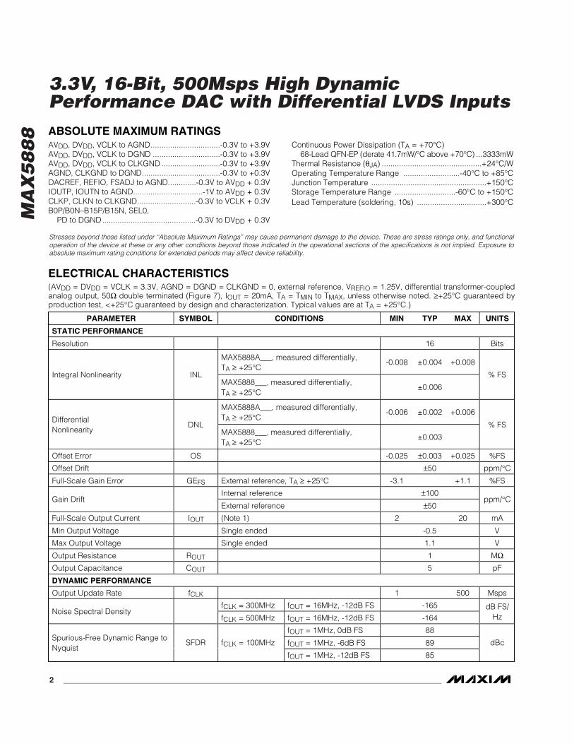
Ordering Information
19-2726; Rev 3; 12/03
For pricing, delivery, and ordering information, please contact Maxim/Dallas Direct! at 1-888-629-4642, or visit Maxim’s website at www.maxim-ic.com.
PART TEMP RANGEPIN-PACKAGE
MAX5888AEGK -40°C to +85°C 68 QFN-EP*
MAX5888EGK -40°C to +85°C 68 QFN-EP*
5859606162 5455565763
38
39
40
41
42
43
44
45
46
47
VCLK
AGND
B6P
QFN
TOP VIEW DGND
DVDD
DGND
B7N
B7P
B8N
B8P
B9N
B9P
5253
B10N
B10P
AVDD
FSAD
J
REFI
O
N.C.
DACR
EF
AGND
AVDD
IOUT
P
IOUT
N
AVDD
AGND
AGND
AVDD
AVDD
B13N
B13P
B14N
B14P
B15N
B15P
DGND
DVDD
SEL0
N.C.
35
36
37 N.C.
N.C.
N.C.
DVDD
DGND
B0N
B0P
B1N
VCLK
CLKGND
CLKN
CLKP
CLKGND
B1P
B2N
B2P
B3N
48 B12P
B3P
64
B6N
656667
B4P
B5N
B5P
68
B4N
2322212019 2726252418 2928 323130
AGND N.C.
3433
49
50 B11P
B12N
51 B11N
11
10
9
8
7
6
5
4
3
2
16
15
14
13
12
1
PD 17
MAX5888
EP
Pin Configuration
*EP = Exposed paddle.
MA
X5
88
8
3.3V, 16-Bit, 500Msps High DynamicPerformance DAC with Differential LVDS Inputs
2 _______________________________________________________________________________________
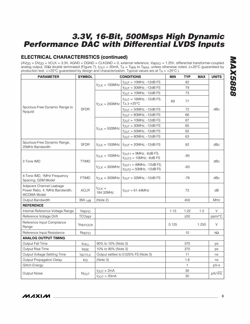
ABSOLUTE MAXIMUM RATINGS
ELECTRICAL CHARACTERISTICS(AVDD = DVDD = VCLK = 3.3V, AGND = DGND = CLKGND = 0, external reference, VREFIO = 1.25V, differential transformer-coupledanalog output, 50Ω double terminated (Figure 7), IOUT = 20mA, TA = TMIN to TMAX, unless otherwise noted. ≥+25°C guaranteed byproduction test, <+25°C guaranteed by design and characterization. Typical values are at TA = +25°C.)
Stresses beyond those listed under “Absolute Maximum Ratings” may cause permanent damage to the device. These are stress ratings only, and functionaloperation of the device at these or any other conditions beyond those indicated in the operational sections of the specifications is not implied. Exposure toabsolute maximum rating conditions for extended periods may affect device reliability.
AVDD, DVDD, VCLK to AGND................................-0.3V to +3.9VAVDD, DVDD, VCLK to DGND ...............................-0.3V to +3.9VAVDD, DVDD, VCLK to CLKGND ...........................-0.3V to +3.9VAGND, CLKGND to DGND....................................-0.3V to +0.3VDACREF, REFIO, FSADJ to AGND.............-0.3V to AVDD + 0.3VIOUTP, IOUTN to AGND................................-1V to AVDD + 0.3VCLKP, CLKN to CLKGND...........................-0.3V to VCLK + 0.3VB0P/B0N–B15P/B15N, SEL0,
PD to DGND...........................................-0.3V to DVDD + 0.3V
Continuous Power Dissipation (TA = +70°C)68-Lead QFN-EP (derate 41.7mW/°C above +70°C) ...3333mW
Thermal Resistance (θJA) ..............................................+24°C/W Operating Temperature Range ..........................-40°C to +85°CJunction Temperature .....................................................+150°CStorage Temperature Range ............................-60°C to +150°CLead Temperature (soldering, 10s) ................................+300°C
PARAMETER SYMBOL CONDITIONS MIN TYP MAX UNITS
STATIC PERFORMANCE
Resolution 16 Bits
MAX5888A___, measured differentially,TA ≥ +25°C
-0.008 ±0.004 +0.008
Integral Nonlinearity INLMAX5888___, measured differentially,TA ≥ +25°C
±0.006
% FS
MAX5888A___, measured differentially,TA ≥ +25°C
-0.006 ±0.002 +0.006DifferentialNonlinearity
DNLMAX5888___, measured differentially,TA ≥ +25°C
±0.003
% FS
Offset Error OS -0.025 ±0.003 +0.025 %FS
Offset Drift ±50 ppm/°C
Full-Scale Gain Error GEFS External reference, TA ≥ +25°C -3.1 +1.1 %FS
Internal reference ±100Gain Drift
External reference ±50ppm/°C
Full-Scale Output Current IOUT (Note 1) 2 20 mA
Min Output Voltage Single ended -0.5 V
Max Output Voltage Single ended 1.1 V
Output Resistance ROUT 1 MΩOutput Capacitance COUT 5 pF
DYNAMIC PERFORMANCE
Output Update Rate fCLK 1 500 Msps
fCLK = 300MHz fOUT = 16MHz, -12dB FS -165Noise Spectral Density
fCLK = 500MHz fOUT = 16MHz, -12dB FS -164dB FS/
Hz
fOUT = 1MHz, 0dB FS 88
fOUT = 1MHz, -6dB FS 89Spurious-Free Dynamic Range toNyquist
SFDR fCLK = 100MHz
fOUT = 1MHz, -12dB FS 85
dBc
MA
X5
88
8
3.3V, 16-Bit, 500Msps High DynamicPerformance DAC with Differential LVDS Inputs
_______________________________________________________________________________________ 3
ELECTRICAL CHARACTERISTICS (continued)(AVDD = DVDD = VCLK = 3.3V, AGND = DGND = CLKGND = 0, external reference, VREFIO = 1.25V, differential transformer-coupledanalog output, 50Ω double terminated (Figure 7), IOUT = 20mA, TA = TMIN to TMAX, unless otherwise noted. ≥+25°C guaranteed byproduction test, <+25°C guaranteed by design and characterization. Typical values are at TA = +25°C.)
PARAMETER SYMBOL CONDITIONS MIN TYP MAX UNITS
fOUT = 10MHz, -12dB FS 82fCLK = 100MHz
fOUT = 30MHz, -12dB FS 79
fOUT = 10MHz, -12dB FS 73
fOUT = 16MHz, -12dB FS,TA ≥ +25°C
69 77
fOUT = 50MHz, -12dB FS 72
fCLK = 200MHz
fOUT = 80MHz, -12dB FS 66
fOUT = 10MHz, -12dB FS 67
fOUT = 30MHz, -12dB FS 65
fOUT = 50MHz, -12dB FS 65
Spurious-Free Dynamic Range toNyquist
SFDR
fCLK = 500MHz
fOUT = 80MHz, -12dB FS 63
dBc
Spurious-Free Dynamic Range,25MHz Bandwidth
SFDR fCLK = 150MHz fOUT = 20MHz, -12dB FS 82 dBc
fCLK = 100MHzfOUT1 = 9MHz, -6dB FS,fOUT2 = 10MHz, -6dB FS
-85
2-Tone IMD TTIMD
fCLK = 300MHzfOU T 1 = 49M H z, - 12d B FS ,fOU T 2 = 50M H z, - 12d B FS
-83
dBc
4-Tone IMD, 1MHz FrequencySpacing, GSM Model
FTIMD fCLK = 300MHz fOUT = 32MHz, -12dB FS -78 dBc
Adjacent Channel LeakagePower Ratio, 4.1MHz Bandwidth,WCDMA Model
ACLRfCLK =184.32MHz
fOUT = 61.44MHz 73 dB
Output Bandwidth BW-1dB (Note 2) 450 MHz
REFERENCE
Internal Reference Voltage Range VREFIO 1.13 1.22 1.3 V
Reference Voltage Drift TCOREF ±50 ppm/°C
Reference Input ComplianceRange
VREFIOCR 0.125 1.250 V
Reference Input Resistance RREFIO 10 kΩANALOG OUTPUT TIMING
Output Fall Time tFALL 90% to 10% (Note 3) 375 ps
Output Rise Time tRISE 10% to 90% (Note 3) 375 ps
Output Voltage Settling Time tSETTLE Output settles to 0.025% FS (Note 3) 11 ns
Output Propagation Delay tPD (Note 3) 1.8 ns
Glitch Energy 1 pV-s
IOUT = 2mA 30Output Noise NOUT
IOUT = 20mA 30pA/√Hz

MA
X5
88
8
3.3V, 16-Bit, 500Msps High DynamicPerformance DAC with Differential LVDS Inputs
4 _______________________________________________________________________________________
ELECTRICAL CHARACTERISTICS (continued)(AVDD = DVDD = VCLK = 3.3V, AGND = DGND = CLKGND = 0, external reference, VREFIO = 1.25V, differential transformer-coupledanalog output, 50Ω double terminated (Figure 7), IOUT = 20mA, TA = TMIN to TMAX, unless otherwise noted. ≥+25°C guaranteed byproduction test, <+25°C guaranteed by design and characterization. Typical values are at TA = +25°C.)
PARAMETER SYMBOL CONDITIONS MIN TYP MAX UNITS
TIMING CHARACTERISTICS
Data to Clock Setup Time tSETUP Referenced to rising edge of clock (Note 4) -0.8 ns
Data to Clock Hold Time tHOLD Referenced to rising edge of clock (Note 4) 1.8 ns
Data Latency 3.5Clockcycles
Minimum Clock Pulse Width High tCH CLKP, CLKN 0.9 nsMinimum Clock Pulse Width Low tCL CLKP, CLKN 0.9 nsLVDS LOGIC INPUTS (B0N–B15N, B0P–B15P)
Differential Input Logic High VIH 100 mV
Differential Input Logic Low VIL -100 mV
Common-Mode Voltage Range VCOM 1.125 1.375 V
Differential Input Resistance RIN 85 100 125 ΩInput Capacitance CIN 5 pF
CMOS LOGIC INPUTS (PD, SEL0)
Input Logic High VIH0.7 DVDD
V
Input Logic Low VIL0.3 DVDD
V
Input Leakage Current IIN -15 +15 µA
Input Capacitance CIN 5 pF
CLOCK INPUTS (CLKP, CLKN)
Sine wave ≥1.5Differential Input Voltage Swing VCLK
Square wave ≥0.5VP-P
Differential Input Slew Rate SRCLK (Note 5) >100 V/µs
Common-Mode Voltage Range VCOM1.5
±20%V
Input Resistance RCLK 5 kΩInput Capacitance CCLK 5 pF
POWER SUPPLIES
Analog Supply Voltage Range AVDD 3.135 3.3 3.465 V
Digital Supply Voltage Range DVDD 3.135 3.3 3.465 V
Clock Supply Voltage Range VCLK 3.135 3.3 3.465 V
fCLK = 100Msps, fOUT = 1MHz 27Analog Supply Current IAVDD
Power-down 0.3mA
fCLK = 100Msps, fOUT = 1MHz 7 mADigital Supply Current IDVDD
Power-down 10 µA
fCLK = 100Msps, fOUT = 1MHz 5.6 mAClock Supply Current IVCLK
Power-down 10 µA

MA
X5
88
8
3.3V, 16-Bit, 500Msps High DynamicPerformance DAC with Differential LVDS Inputs
_______________________________________________________________________________________ 5
Note 1: Nominal full-scale current IOUT = 32 IREF. Note 2: This parameter does not include update-rate depending effects of sin(x)/x filtering inherent in the MAX5888.Note 3: Parameter measured single ended into a 50Ω termination resistor.Note 4: Parameter guaranteed by design.Note 5: A differential clock input slew rate of >100V/ms is required to achieve the specified dynamic performance.Note 6: Parameter defined as the change in midscale output caused by a ±5% variation in the nominal supply voltage.
PARAMETER SYMBOL CONDITIONS MIN TYP MAX UNITS
fCLK = 100Msps, fOUT = 1MHz 130Power Dissipation PDISS
Power-down 1mW
Power-Supply Rejection Ratio PSRR AVDD = VCLK = DVDD = 3.3V ±5% (Note 6) -1 +1 %FS/V
ELECTRICAL CHARACTERISTICS (continued)(AVDD = DVDD = VCLK = 3.3V, AGND = DGND = CLKGND = 0, external reference, VREFIO = 1.25V, differential transformer-coupledanalog output, 50Ω double terminated (Figure 7), IOUT = 20mA, TA = TMIN to TMAX, unless otherwise noted. ≥+25°C guaranteed byproduction test, <+25°C guaranteed by design and characterization. Typical values are at TA = +25°C.)
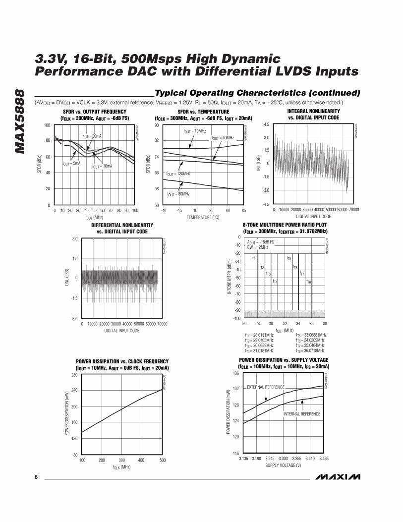
Typical Operating Characteristics(AVDD = DVDD = VCLK = 3.3V, external reference, VREFIO = 1.25V, RL = 50Ω, IOUT = 20mA, TA = +25°C, unless otherwise noted.)
0
30
20
10
40
50
60
70
80
90
100
0 2010 30 40 50
SPURIOUS-FREE DYNAMIC RANGEvs. OUTPUT FREQUENCY (fCLK = 100MHz)
MAX
5888
toc0
1
fOUT (MHz)
SFDR
(dBc
)
-12dB FS
0dB FS
-6dB FS
0
30
20
10
40
50
60
70
80
90
100
0 4020 30 50 70 9010 60 80 100
SPURIOUS-FREE DYNAMIC RANGEvs. OUTPUT FREQUENCY (fCLK = 200MHz)
MAX
5888
toc0
2
fOUT (MHz)
SFDR
(dBc
)
-6dB FS
-12dB FS0dB FS
0
30
20
10
40
50
60
70
80
90
100
0 10050 150 200 250
SPURIOUS-FREE DYNAMIC RANGEvs. OUTPUT FREQUENCY (fCLK = 500MHz)
MAX
5888
toc0
3
fOUT (MHz)
SFDR
(dBc
)
-6dB FS
0dB FS
-12dB FS
-100
-70
-80
-90
-60
-50
-40
-30
-20
-10
0
7 98 10 11 12
2-TONE INTERMODULATION DISTORTION (fCLK = 100MHz)
MAX
5888
toc0
4
fOUT (MHz)
2-TO
NE IM
D (d
Bm)
2 x fT1 - fT2 2 x fT2 - fT1
fT2 fT1
AOUT = -6dB FSBW = 5MHz
fT1 = 9.0252MHzfT2 = 10.0417MHz
-40
-60
-50
-80
-70
-90
-100
0
2-TONE IMD vs. OUTPUT FREQUENCY(1MHz CARRIER SPACING, fCLK = 300MHz)
MAX
5888
toc0
5
fOUT (MHz)
TWO-
TONE
IMD
(dBc
)
5025 75 100
-6dB FS
-12dB FS
-100
-70
-80
-90
-60
-50
-40
-30
-20
-10
0
77 7978 80 81 82
2-TONE INTERMODULATION DISTORTION (fCLK = 450MHz)
MAX
5888
toc0
6
fOUT (MHz)
2-TO
NE IM
D (d
Bm)
2 x fT1 - fT2 2 x fT2 - fT1
fT2 fT1
AOUT = -6dB FSBW = 5MHz
fT1 = 79.2114MHzfT2 = 80.0903MHz
MA
X5
88
8
3.3V, 16-Bit, 500Msps High DynamicPerformance DAC with Differential LVDS Inputs
6 _______________________________________________________________________________________
Typical Operating Characteristics (continued)(AVDD = DVDD = VCLK = 3.3V, external reference, VREFIO = 1.25V, RL = 50Ω, IOUT = 20mA, TA = +25°C, unless otherwise noted.)
50
58
66
74
82
90
SFDR vs. TEMPERATURE(fCLK = 300MHz, AOUT = -6dB FS, IOUT = 20mA)
MAX
5888
toc0
8
TEMPERATURE (°C)
SFDR
(dBc
)
-40 10-15 6035 85
fOUT = 80MHz
fOUT = 120MHz
fOUT = 10MHzfOUT = 40MHz
0
20
40
60
80
100
SFDR vs. OUTPUT FREQUENCY(fCLK = 200MHz, AOUT = -6dB FS)
MAX
5888
toc0
7
fOUT (MHz)
SFDR
(dBc
)
0 402010 30 50 70 908060 100
IOUT = 20mA
IOUT = 5mAIOUT = 10mA
-3.0
-1.5
0
1.5
3.0
DIFFERENTIAL NONLINEARTIYvs. DIGITAL INPUT CODE
MAX
5888
toc1
0
DIGITAL INPUT CODE
DNL
(LSB
)
0 300002000010000 5000040000 7000060000
-4.5
-3.0
-1.5
0
1.5
3.0
4.5
INTEGRAL NONLINEARITYvs. DIGITAL INPUT CODE
MAX
5888
toc9
DIGITAL INPUT CODE
INL
(LSB
)
0 300002000010000 5000040000 7000060000
-100
-70
-80
-90
-60
-50
-40
-30
-20
-10
0
26 3028 3432 36 38
8-TONE MULTITONE POWER RATIO PLOT (fCLK = 300MHz, fCENTER = 31.9702MHz)
MAX
5888
toc1
1fOUT (MHz)
8-TO
NE M
TPR
(dBm
)
fT2 fT6fT3 fT7
fT4 fT8
fT1 fT5
AOUT = -18dB FSBW = 12MHz
fT1 = 28.0151MHzfT2 = 29.0405MHzfT3 = 30.0659MHzfT4 = 31.0181MHz
fT5 = 33.06881MHzfT6 = 34.0209MHzfT7 = 35.0464MHzfT8 = 36.0718MHz
80
120
160
200
240
280
POWER DISSIPATION vs. CLOCK FREQUENCY(fOUT = 10MHz, AOUT = 0dB FS, IOUT = 20mA)
MAX
5888
toc1
2
fCLK (MHz)
POW
ER D
ISSI
PATI
ON (m
W)
100 300200 400 500116
120
124
128
132
136
POWER DISSIPATION vs. SUPPLY VOLTAGE(fCLK = 100MHz, fOUT = 10MHz, IFS = 20mA)
MAX
5888
toc1
3
SUPPLY VOLTAGE (V)
POW
ER D
ISSI
PATI
ON (m
W)
3.135 3.3003.2453.190 3.355 3.410 3.465
EXTERNAL REFERENCE
INTERNAL REFERENCE
MA
X5
88
8
3.3V, 16-Bit, 500Msps High DynamicPerformance DAC with Differential LVDS Inputs
_______________________________________________________________________________________ 7
Pin Description
PIN NAME FUNCTION
1 B3P Data Bit 3
2 B3N Complementary Data Bit 3
3 B2P Data Bit 2
4 B2N Complementary Data Bit 2
5 B1P Data Bit 1
6 B1N Complementary Data Bit 1
7 B0P Data Bit 0 (LSB)
8 B0N Complementary Data Bit 0 (LSB)
9, 41, 60, 62 DGND Digital Ground
10, 40, 61 DVDDDigital Supply Voltage. Accepts a supply voltage range of 3.135V to 3.465V. Bypass each pin with a0.1µF capacitor to the nearest DGND.
11, 16 VCLKClock Supply Voltage. Accepts a supply voltage range of 3.135V to 3.465V. Bypass each pin with a0.1µF capacitor to the nearest CLKGND.
12, 15 CLKGND Clock Ground
13 CLKP Converter Clock Input. Positive input terminal for the differential converter clock.
14 CLKN Complementary Converter Clock Input. Negative input terminal for the differential converter clock.
17 PDPower-Down Input. PD pulled high enables the DAC’s power-down mode. PD pulled low allows fornormal operation of the DAC. This pin features an internal pulldown resistor.
18, 24, 29,30, 32
AVDDAnalog Supply Voltage. Accepts a supply voltage range of 3.135V to 3.465V. Bypass each pin with a0.1µF capacitor to the nearest AGND.
19, 25, 28,31, 33, EP
AGND Analog Ground. Exposed paddle (EP) must be connected to AGND.
20 REFIOReference I/O. Output of the internal 1.2V precision bandgap reference. Bypass with a 1µF capacitorto AGND. Can be driven with an external reference source.
21 FSADJFull-Scale Adjust Input. This input sets the full-scale output current of the DAC. For 20mA full-scaleoutput current, connect a 2kΩ resistor between FSADJ and DACREF.
22 DACREFReturn Path for the Current Set Resistor. For 20mA full-scale output current, connect a 2kΩ resistorbetween FSADJ and DACREF.
23, 34–38 N.C. Not Connected. Do not connect to these pins. Do not tie these pins together.
26 IOUTNComplementary DAC Output. Negative terminal for differential current output. The full-scale outputcurrent range can be set from 2mA to 20mA.
27 IOUTPDAC Output. Positive terminal for differential current output. The full-scale output current range canbe set from 2mA to 20mA.
39 SEL0Mode Select Input SEL0. Set high to activate the segment shuffling function. Since this pin features aninternal pulldown resistor, it can be left open or pulled low to disable the segment-shuffling function.See Segment Shuffling in the Detailed Description section for more information.
42 B15P Data Bit 15 (MSB)
43 B15N Complementary Data Bit 15 (MSB)
44 B14P Data Bit 14

MA
X5
88
8
3.3V, 16-Bit, 500Msps High DynamicPerformance DAC with Differential LVDS Inputs
8 _______________________________________________________________________________________
Detailed DescriptionArchitecture
The MAX5888 is a high-performance, 16-bit, current-steering DAC (Figure 1) capable of operating with clockspeeds up to 500MHz. The converter consists of sepa-rate input and DAC registers, followed by a current-steering circuit. This circuit is capable of generatingdifferential full-scale currents in the range of 2mA to20mA. An internal current-switching network in combi-nation with external 50Ω termination resistors convertthe differential output currents into a differential outputvoltage with a peak-to-peak output voltage range of0.1V to 1V. An integrated 1.2V bandgap reference, con-trol amplifier, and user-selectable external resistordetermine the data converter’s full-scale output range.
Reference Architecture and OperationThe MAX5888 supports operation with the on-chip 1.2Vbandgap reference or an external reference voltagesource. REFIO serves as the input for an external, low-impedance reference source, and as the output if theDAC is operating with the internal reference. For stable
operation with the internal reference, REFIO should bedecoupled to AGND with a 0.1µF capacitor. Due to itslimited output drive capability REFIO must be bufferedwith an external amplifier, if heavier loading is required.
The MAX5888’s reference circuit (Figure 2) employs acontrol amplifier, designed to regulate the full-scalecurrent IOUT for the differential current outputs of theDAC. Configured as a voltage-to-current amplifier, theoutput current can be calculated as follows:
IOUT = 32 IREFIO - 1LSB
IOUT = 32 IREFIO - (IOUT / 216)
where IREFIO is the reference output current (IREFIO =VREFIO/RSET) and IOUT is the full-scale output current ofthe DAC. Located between FSADJ and DACREF, RSETis the reference resistor, which determines the amplifi-er’s output current for the DAC. See Table 1 for a matrixof different IOUT and RSET selections.
PIN NAME FUNCTION
45 B14N Complementary Data Bit 14
46 B13P Data Bit 13
47 B13N Complementary Data Bit 13
48 B12P Data Bit 12
49 B12N Complementary Data Bit 12
50 B11P Data Bit 11
51 B11N Complementary Data Bit 11
52 B10P Data Bit 10
53 B10N Complementary Data Bit 10
54 B9P Data Bit 9
55 B9N Complementary Data Bit 9
56 B8P Data Bit 8
57 B8N Complementary Data Bit 8
58 B7P Data Bit 7
59 B7N Complementary Data Bit 7
63 B6P Data Bit 6
64 B6N Complementary Data Bit 6
65 B5P Data Bit 5
66 B5N Complementary Data Bit 5
67 B4P Data Bit 4
68 B4N Complementary Data Bit 4
Pin Description (continued)

MA
X5
88
8
3.3V, 16-Bit, 500Msps High DynamicPerformance DAC with Differential LVDS Inputs
_______________________________________________________________________________________ 9
Analog Outputs (IOUTP, IOUTN)The MAX5888 outputs two complementary currents(IOUTP, IOUTN) that can be operated in a single-ended or differential configuration. A load resistor canconvert these two output currents into complementarysingle-ended output voltages. The differential voltageexisting between IOUTP and IOUTN can also be con-
verted to a single-ended voltage using a transformer ora differential amplifier configuration. If no transformer isused, the output should have a 50Ω termination to theanalog ground and a 50Ω resistor between the outputs.
Although not recommended, because of additionalnoise pickup from the ground plane, for single-ended
1.2VREFERENCE
CURRENT-STEERINGDAC
FUNCTIONSELECTION
BLOCK
AGND
SEL0DGNDDVDD
REFIO
REFADJ
CLKNCLKP
PD
AVDD
IOUTPIOUTN
SEGMENT SHUFFLING/LATCH
DECODER
LVDS RECEIVER INPUT/LATCH
16
DIFFERENTIAL DIGITAL INPUT B0 THROUGH B15
MAX5888
Figure 1. Simplified MAX5888 Block Diagram
RSET (kΩ)FULL-SCALE CURRENTIOUT (mA)
REFERENCE CURRENTIREF (µA) CALCULATED 1% EIA STD
OUTPUT VOLTAGEVIOUTP/N* (mVP-P)
2 62.5 19.2 19.1 100
5 156.25 7.68 7.5 250
10 312.5 3.84 3.83 500
15 468.75 2.56 2.55 750
20 625 1.92 1.91 1000
Table 1. IOUT and RSET Selection Matrix Based on a Typical 1.200V Reference Voltage
*Terminated into a 50Ω load.

MA
X5
88
8
3.3V, 16-Bit, 500Msps High DynamicPerformance DAC with Differential LVDS Inputs
10 ______________________________________________________________________________________
operation IOUTP should be selected as the output, withIOUTN connected to AGND. Note that a single-endedoutput configuration has a higher 2nd-order harmonicdistortion at high output frequencies than a differentialoutput configuration.
Figure 3 displays a simplified diagram of the internaloutput structure of the MAX5888.
Clock Inputs (CLKP, CLKN)The MAX5888 features a flexible differential clock input(CLKP, CLKN) operating from separate supplies(VCLK, CLKGND) to achieve the lowest possible jitterperformance. The two clock inputs can be driven froma single-ended or a differential clock source. For sin-gle-ended operation, CLKP should be driven by a logicsource, while CLKN should be bypassed to AGND witha 0.1µF capacitor.
The CLKP and CLKN pins are internally biased to 1.5V.This allows the user to AC-couple clock sources directlyto the device without external resistors to define the DClevel. The input resistance of CLKP and CLKN is >5kΩ.
See Figure 4 for a convenient and quick way to apply adifferential signal created from a single-ended source(e.g., HP 8662A signal generator) and a widebandtransformer. These inputs can also be driven from anLVDS-compatible clock source; however, it is recom-mended to use sinewave or AC-coupled ECL drive forbest performance.
Data Timing RelationshipFigure 5 shows the timing relationship between differ-ential, digital LVDS data, clock, and output signals. TheMAX5888 features a 1.4ns hold, a -1ns setup, and a1.8ns propagation delay time. There is a 3.5 clock-cycle latency between CLKP/CLKN transitioninghigh/low and IOUTP/IOUTN.
LVDS-Compatible Digital Inputs(B0P–B15P, B0N–B15N)
The MAX5888 features LVDS receivers on the bus inputinterface. These LVDS inputs (B0P/N through B15P/N)allow for a low-differential voltage swing with low con-stant power consumption across a large range of
0.1µF
1.2VREFERENCE
10kΩ
IREF
RSET
DACREF
FSADJ
REFIO
IREF = VREFIO/RSET
CURRENT-STEERINGDAC
AVDD
IOUTP
IOUTN
Figure 2. Reference Architecture, Internal ReferenceConfiguration
IOUTIOUT
IOUTN IOUTP
CURRENTSOURCES
CURRENTSWITCHES
AVDD
Figure 3. Simplified Analog Output Structure
SINGLE-ENDEDCLOCK SOURCE(e.g., HP 8662A)
1:1
WIDEBAND RF TRANSFORMERPERFORMS SINGLE-ENDED TODIFFERENTIAL CONVERSION.
TODAC
CLKP
0.1µF
0.1µF CLKN
CLKGND
25Ω
25Ω
Figure 4. Differential Clock Signal Generation

MA
X5
88
8
3.3V, 16-Bit, 500Msps High DynamicPerformance DAC with Differential LVDS Inputs
______________________________________________________________________________________ 11
frequencies. Their differential characteristic supportsthe transmission of high-speed data patterns withoutthe negative effects of electromagnetic interference(EMI). All MAX5888 LVDS inputs feature on-chip termi-nation with differential 100Ω resistors. See Figure 6 fora simplified block diagram of the LVDS inputs.
A common-mode level of 1.25V and an 800mV differen-tial input swing can be applied to these inputs.
Segment Shuffling (SEL0)Segment shuffling can improve the SFDR of theMAX5888. The improvement is most pronounced athigher output frequencies and amplitudes. Note that animprovement in SFDR can only be achieved at the costof a slight increase in the DAC’s noise floor.
Pin SEL0 controls the segment-shuffling function. IfSEL0 is pulled low, the segment-shuffling function ofthe DAC is disabled. SEL0 can also be left open,because an internal pulldown resistor helps to deacti-vate the segment-shuffling feature. To activate theMAX5888 segment-shuffling function, SEL0 must bepulled high.
Power-Down Operation (PD)The MAX5888 also features an active-high power-downmode, which allows the user to cut the DAC’s digitalcurrent consumption to less than 6µA and the analogcurrent consumption to less than 0.3mA. A single pin(PD) is used to control the power-down mode (PD = 1)or reactivate the DAC (PD = 0) after power-down.
Enabling the power-down mode of the MAX5888 allowsthe overall power consumption to be reduced to lessthan 1mW. The MAX5888 requires 10ms to wake upfrom power-down and enter a fully operational state.
Applications InformationDifferential Coupling Using a
Wideband RF TransformerThe differential voltage existing between IOUTP andIOUTN can also be converted to a single-ended volt-age using a transformer (Figure 7) or a differentialamplifier configuration. Using a differential transformercoupled output, in which the output power is limited to0dBm, can optimize the dynamic performance.However, make sure to pay close attention to the trans-former core saturation characteristics when selecting atransformer for the MAX5888. Transformer core satura-tion can introduce strong 2nd-harmonic distortion,especially at low output frequencies and high signal
B0 TO B15
CLKN
CLKP
IOUT
N
DIGITAL DATA IS LATCHED ONTHE RISING EDGE OF CLKP
OUTPUT DATA IS UPDATED ONTHE FALLING EDGE OF CLKP
N + 1 N + 2
N - 5 N - 3 N - 1N - 2N - 4
tSETUP tHOLD
tPD
tCH tCL
N - 1
Figure 5. Detailed Timing Relationship
100Ω
B0P–B15P
B0N–B15N
D Q
D Q
CLOCK
TO DECODELOGIC
Figure 6. Simplified LVDS-Compatible Input Structure

MA
X5
88
8
3.3V, 16-Bit, 500Msps High DynamicPerformance DAC with Differential LVDS Inputs
12 ______________________________________________________________________________________
amplitudes. It is also recommended to center tap thetransformer to ground. If no transformer is used, eachDAC output should be terminated to ground with a 50Ωresistor. Additionally, a 100Ω resistor should be placedbetween the outputs (Figure 8).
If a single-ended unipolar output is desirable, IOUTPshould be selected as the output, with IOUTN ground-ed. However, driving the MAX5888 single ended is notrecommended since additional noise is added (fromthe ground plane) in such configurations.
The distortion performance of the DAC depends on theload impedance. The MAX5888 is optimized for a 50Ωdouble termination. It can be used with a transformeroutput as shown in Figure 7 or just one 50Ω resistorfrom each output to ground and one 50Ω resistorbetween the outputs. This produces a full-scale outputpower of up to 0dBm depending on the output currentsetting. Higher termination impedance can be used atthe cost of degraded distortion performance andincreased output noise voltage.
Adjacent Channel Leakage Power Ratio(ACLR) Testing for CDMA- and
WCDMA-Based Base Station Transceiver Systems (BTS)
The transmitter sections of BTS applications servingCDMA and WCDMA architectures must generate carri-ers with minimal coupling of carrier energy into the adja-cent channels. Similar to the GSM/EDGE model (see theMultitone Testing for GSM/EDGE Applications section inthe Applications section), a transmit mask (Tx mask)exists for this application. The spread-spectrum modula-tion function applied to the carrier frequency generates aspectral response, which is uniform over a given band-width (up to 4MHz) for a WCDMA-modulated carrier.
A dominant specification is ACLR, a parameter whichreflects the ratio of the power in the desired carrierband to the power in an adjacent carrier band. Thespecification covers the first two adjacent bands, and ismeasured on both sides of the desired carrier.
According to the transmit mask for CDMA and WCDMAarchitectures, the power ratio of the integrated carrierchannel energy to the integrated adjacent channelenergy must be >45dB for the first adjacent carrier slot(ACLR 1) and >50dB for the second adjacent carrierslot (ACLR 2). This specification applies to the output ofthe entire transmitter signal chain. The requirement foronly the DAC block of the transmitter must be tighter,with a typical margin of >15dB, requiring the DAC’sACLR 1 to be better than 60dB. Adjacent channel leak-age is caused by a single-spread spectrum carrier,which generates intermodulation (IM) productsbetween the frequency components located within thecarrier band. The energy at one end of the carrier bandgenerates IM products with the energy from the oppo-site end of the carrier band. For single-carrier WCDMAmodulation, these IMD products are spread 3.84MHzover the adjacent sideband. Four contiguous WCDMA
MAX5888
T2, 1:1
T1, 1:1
VOUT, SINGLE ENDED
WIDEBAND RF TRANSFORMER T2PERFORMS THE DIFFERENTIAL TO
SINGLE-ENDED CONVERSION.
50Ω
100Ω
50Ω
IOUTP
IOUTN
B0–B15
16
AVDD DVDD VCLK
AGND DGND CLKGND
Figure 7. Differential to Single-Ended Conversion Using a Wideband RF Transformer
MAX5888
50Ω
100Ω
50Ω
IOUTP
IOUTN
B0–B15
16
AVDD DVDD VCLK
AGND DGND CLKGND
OUTP
OUTN
Figure 8. MAX5888 Differential Output Configuration

MA
X5
88
8
3.3V, 16-Bit, 500Msps High DynamicPerformance DAC with Differential LVDS Inputs
______________________________________________________________________________________ 13
carriers spread their IM products over a bandwidth of20MHz on either side of the 20MHz total carrier band-width. In this four-carrier scenario, only the energy inthe first adjacent 3.84MHz side band is considered forACLR 1. To measure ACLR, drive the converter with aWCDMA pattern. Make sure that the signal is backedoff by the peak-to-average ratio, such that the DAC isnot clipping the signal. ACLR can then be measuredwith the ACLR measurement function built into yourspectrum analyzer.
Figure 9 shows the ACLR performance for a singleWCDMA carrier (fCLK = 184.32MHz, fOUT = 61.44MHz)applied to the MAX5888 (including measurement sys-tem limitations*).
Figure 10 illustrates the ACLR test results for theMAX5888 with a four-carrier WCDMA signal at an out-put frequency of 61.44MHz and sampling frequency of184.32MHz. Again, the noise floor of the instrumentrestricts the signal’s real dynamic range of the signal,and the measured ACLR 1 understates the actual bymore than 2.5dB. Considerable care must be taken toensure accurate measurement of this parameter.
Multitone Testing for GSM/EDGEApplications
The transmitter sections of multicarrier base stationtransceiver systems for GSM/EDGE usually presentcommunication DAC manufacturers with the difficulttask of providing devices with higher resolution, whilesimultaneously reducing noise and spurious emissionsover a desired bandwidth.
To specify noise and spurious emissions from base sta-tions, a GSM/EDGE Tx mask is used to identify the DACrequirements for these parameters. This mask showsthat the allowable levels for noise and spurious emis-sions are dependent on the offset frequency from thetransmitted carrier frequency. The GSM/EDGE maskand its specifications are based on a single active car-rier with any other carriers in the transmitter being dis-abled. Specifications displayed in Figure 11 supportper-carrier output power levels of 20W or greater.Lower output power levels yield less stringent emissionrequirements. For GSM/EDGE applications, the DACdemands spurious emission levels of less than -80dBcfor offset frequencies ≥6MHz. Spurious products fromthe DAC can combine with both random noise and spu-rious products from other circuit elements. The spuri-ous products from the DAC should therefore be backedoff by 6dB more to allow for these other sources andstill avoid signal clipping.
*Note that due to their own IM effects and noise limitations, spectrum analyzers introduce ACLR errors, which can falsify the measure-ment. For a single-carrier ACLR measurement greater than 70dB, these measurement limitations are significant, becoming even morerestricting for multicarrier measurement. Before attempting an ACLR measurement, it is recommended consulting application notes pro-vided by major spectrum analyzer manufacturers that provide useful tips on how to use their instruments for such tests.
-125
-100
-110
-120
-90
-80
-70
-60
-50
-30
-40
OUTP
UT P
OWER
(dBm
)
-25
3.5MHz/div
fCENTER = 61.44MHzfCLK = 184.32Mbps
ACLR = 73dB
Figure 9. ACLR for WCDMA Modulation, Single Carrier
-130
-100
-110
-120
-90
-80
-70
-60
-50
-30
-40
3.5MHz/div
fCENTER = 61.44MHzfCLK = 184.32MbpsACLR = 65dB
OUTP
UT P
OWER
(dBm
)
Figure 10. ACLR for WCDMA Modulation, Four Carriers

MA
X5
88
8
3.3V, 16-Bit, 500Msps High DynamicPerformance DAC with Differential LVDS Inputs
14 ______________________________________________________________________________________
The number of carriers and their signal levels withrespect to the full scale of the DAC are important aswell. Unlike a full-scale sine wave, the inherent nature ofa multitone signal contains higher peak-to-RMS ratios,raising the prospect for potential clipping, if the signallevel is not backed off appropriately. If a transmitteroperates with four/eight in-band carriers, each individ-ual carrier must be operated at less than -12dB FS/-18dB FS to avoid waveform clipping.
The noise density requirements (Table 2) for aGSM/EDGE-based system can again be derived fromthe system’s Tx mask. With a worst-case noise level of -80dBc at frequency offsets of ≥6MHz and a measure-ment bandwidth of 100kHz, the minimum noise densityper hertz is calculated as follows:
SNRMIN = -80dBc - 10 log10(100 103Hz)
SNRMIN = -130dBc/Hz
Since random DAC noise adds to both the spurious tonesand to random noise from other circuit elements, it is rec-ommended reducing the specification limits by about10dB to allow for these additional noise contributionswhile maintaining compliance with the Tx mask values.
Other key factors in selecting the appropriate DAC forthe Tx path of a multicarrier GSM/EDGE system is theconverter’s ability to offer superior IMD and MTPR perfor-mance. Multiple carriers in a designated band generateunwanted intermodulation distortion between the individ-ual carrier frequencies. A multitone test vector usuallyconsists of several equally spaced carriers, usually four,with identical amplitudes. Each of these carriers is rep-resentative of a channel within the defined bandwidth ofinterest. To verify MTPR, one or more tones areremoved such that the intermodulation distortion perfor-
mance of the DAC can be evaluated. Nonlinearitiesassociated with the DAC create spurious tones, someof which may fall back into the area of the removedtone, limiting a channel’s carrier-to-noise ratio. Otherspurious components falling outside the band of inter-est can also be important, depending on the system’sspectral mask and filtering requirements. Going back tothe GSM/EDGE Tx mask, the IMD specification for adja-cent carriers varies somewhat among the different GSMstandards. For the PCS1800 and GSM850 standards,the DAC must meet an average IMD of -70dBc.
Table 3 summarizes the dynamic performance require-ments for the entire Tx signal chain in a four-carrierGSM/EDGE-based system and compares the previous-ly established converter requirements with a new-gen-eration high dynamic performance DAC.
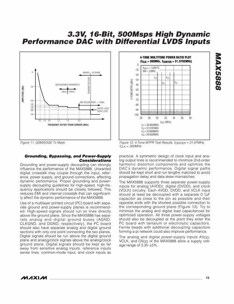
The four-tone MTPR plot in Figure 12 demonstrates theMAX5888’s excellent dynamic performance. The centerfrequency (fCENTER = 31.97MHz) has been removed toallow detection and analysis of intermodulation or spuri-ous components falling back into this empty spot fromadjacent channels. The four carriers are observed overa 12MHz bandwidth and are equally spaced at 1MHz.Each individual output amplitude is backed off to -12dBFS. Under these conditions, the DAC yields an MTPRperformance of -78dBc.
NUMBER OFCARRIERS
CARRIERPOWER LEVEL
(dB FS)
DAC NOISE DENSITYREQUIREMENT
(dB FS/Hz)
2 -6 -146
4 -12 -152
8 -18 -158
Table 2. GSM/EDGE Noise Requirementsfor Multicarrier Systems
SPECIFICATIONSYSTEM TRANSMITTER
OUTPUT LEVELSDAC REQUIREMENTS WITH
MARGINSMAX5888 SPECIFICATIONS
SFDR 80dBc 86dBc 82dBc*
SNR -130dBc/Hz -152dB FS/Hz -165dB/Hz
IMD -70dBc -75dBc -78dBc
Carrier Amplitude N/S -12dB FS -12dB FS
Table 3. Summary of Important AC Performance Parameters for Multicarrier GSM/EDGESystems
*Measured within a 25MHz window.
MA
X5
88
8
3.3V, 16-Bit, 500Msps High DynamicPerformance DAC with Differential LVDS Inputs
______________________________________________________________________________________ 15
Grounding, Bypassing, and Power-SupplyConsiderations
Grounding and power-supply decoupling can stronglyinfluence the performance of the MAX5888. Unwanteddigital crosstalk may couple through the input, refer-ence, power supply, and ground connections, affectingdynamic performance. Proper grounding and power-supply decoupling guidelines for high-speed, high-fre-quency applications should be closely followed. Thisreduces EMI and internal crosstalk that can significant-ly affect the dynamic performance of the MAX5888.
Use of a multilayer printed circuit (PC) board with sepa-rate ground and power-supply planes is recommend-ed. High-speed signals should run on lines directlyabove the ground plane. Since the MAX5888 has sepa-rate analog and digital ground buses (AGND,CLKGND, and DGND, respectively), the PC boardshould also have separate analog and digital groundsections with only one point connecting the two planes.Digital signals should be run above the digital groundplane and analog/clock signals above the analog/clockground plane. Digital signals should be kept as faraway from sensitive analog inputs, reference inputssense lines, common-mode input, and clock inputs as
practical. A symmetric design of clock input and ana-log output lines is recommended to minimize 2nd-orderharmonic distortion components and optimize theDAC’s dynamic performance. Digital signal pathsshould be kept short and run lengths matched to avoidpropagation delay and data skew mismatches.
The MAX5888 supports three separate power-supplyinputs for analog (AVDD), digital (DVDD), and clock(VCLK) circuitry. Each AVDD, DVDD, and VCLK inputshould at least be decoupled with a separate 0.1µFcapacitor as close to the pin as possible and theiropposite ends with the shortest possible connection tothe corresponding ground plane (Figure 13). Try tominimize the analog and digital load capacitances foroptimized operation. All three power-supply voltagesshould also be decoupled at the point they enter thePC board with tantalum or electrolytic capacitors.Ferrite beads with additional decoupling capacitorsforming a pi network could also improve performance.
The analog and digital power-supply inputs AVDD,VCLK, and DVDD of the MAX5888 allow a supply volt-age range of 3.3V ±5%.
O
-30
-60
-70-73-75-80
-90
0.2 0.4 0.6 1.2 1.8 6.0
IMD REQUIREMENT: < -70dBc
30kHz 100kHz
MEASUREMENT BANDWIDTH
TRAN
SMIT
TER
EDGE
INBAND OUTBAND
WORST-CASENOISE LEVEL
AMPL
ITUD
E (d
Bc)
FREQUENCY OFFSET FROM CARRIER (MHz)
Figure 11. GSM/EDGE Tx Mask
-100
-70
-80
-90
-60
-50
-40
-30
-20
-10
0
26 3028 3432 36 38
4-TONE MULTITONE POWER RATIO PLOT (fCLK = 300MHz, fCENTER = 31.9702MHz)
fOUT (MHz)
4-TO
NE M
TPR
(dBm
)
fT2
fT3
fT4
fT1
AOUT = -12dB FSBW = 12MHz
fT1 = 30.0659MHzfT2 = 31.0181MHzfT3 = 33.0688MHzfT4 = 34.0209MHz
Figure 12. 4-Tone MTPR Test Results, fCENTER = 31.97MHz, fCLK = 300MHz

MA
X5
88
8
3.3V, 16-Bit, 500Msps High DynamicPerformance DAC with Differential LVDS Inputs
16 ______________________________________________________________________________________
The MAX5888 is packaged in a 68-lead QFN-EP package (package code: G6800-4), providing greaterdesign flexibility, increased thermal efficiency**, andoptimized AC performance of the DAC. The exposedpad (EP) enables the user to implement groundingtechniques, which are necessary to ensure highest per-formance operation. The EP must be soldered downto AGND.
In this package, the data converter die is attached toan EP lead frame with the back of this frame exposed atthe package bottom surface, facing the PC board sideof the package. This allows a solid attachment of thepackage to the PC board with standard infrared (IR)flow soldering techniques. A specially created land pat-tern on the PC board, matching the size of the EP (6mm 6mm), ensures the proper attachment and groundingof the DAC. Designing vias*** into the land area andimplementing large ground planes in the PC boarddesign allow for highest performance operation of the
DAC. An array of at least 4 4 vias (≤0.3mm diameterper via hole and 1.2mm pitch between via holes) is rec-ommended for this 68-lead QFN-EP package.
Static Performance Parameter DefinitionsIntegral Nonlinearity (INL)
Integral nonlinearity is the deviation of the values on anactual transfer function from either a best straight line fit(closest approximation to the actual transfer curve) or aline drawn between the end points of the transfer func-tion, once offset and gain errors have been nullified. Fora DAC, the deviations are measured at every individualstep.
Differential Nonlinearity (DNL)Differential nonlinearity is the difference between anactual step height and the ideal value of 1 LSB. A DNLerror specification of less than 1 LSB guarantees nomissing codes and a monotonic transfer function.
FERRITE BEAD
AVDD
1µF 10µF 47µFANALOG POWER-SUPPLY SOURCE
FERRITE BEAD
DVDD
1µF 10µF 47µFDIGITAL POWER-SUPPLY SOURCE
FERRITE BEAD
VCLK
1µF 10µF 47µFCLOCK POWER-SUPPLY SOURCE
AVDD
AGND
MAX5888
B0–B15
16
0.1µF
DGND
0.1µF
VCLK
CLKGND
0.1µF
OUTP
OUTN
DVDD
BYPASSING—DAC LEVEL BYPASSING—BOARD LEVEL
Figure 13. Recommended Power-Supply Decoupling and Bypassing Circuitry
**Thermal efficiency is not the key factor, since the MAX5888 features low-power operation. The exposed pad is the key element toensure a solid ground connection between the DAC and the PC board’s analog ground layer.
***Vias connect the land pattern to internal or external copper planes. It is important to connect as many vias as possible to the analogground plane to minimize inductance.

MA
X5
88
8
3.3V, 16-Bit, 500Msps High DynamicPerformance DAC with Differential LVDS Inputs
______________________________________________________________________________________ 17
Offset ErrorThe offset error is the difference between the ideal andthe actual offset current. For a DAC, the offset point isthe value at the output for the two midscale digital inputcodes with respect to the full scale of the DAC. Thiserror affects all codes by the same amount.
Gain ErrorA gain error is the difference between the ideal and theactual full-scale output voltage on the transfer curve,after nullifying the offset error. This error alters the slopeof the transfer function and corresponds to the samepercentage error in each step.
Settling TimeThe settling time is the amount of time required from thestart of a transition until the DAC output settles its newoutput value to within the converter’s specified accuracy.
Glitch EnergyGlitch impulses are caused by asymmetrical switchingtimes in the DAC architecture, which generates unde-sired output transients. The amount of energy thatappears at the DAC’s output is measured over time andusually specified in the pV-s range.
Dynamic Performance ParameterDefinitions
Signal-to-Noise Ratio (SNR)For a waveform perfectly reconstructed from digital sam-ples, the theoretical maximum SNR is the ratio of the full-scale analog output (RMS value) to the RMS quantizationerror (residual error). The ideal, theoretical minimum canbe derived from the DAC’s resolution (N bits):
SNRdB = 6.02dB N + 1.76dB
However, noise sources such as thermal noise, refer-ence noise, clock jitter, etc., affect the ideal reading;therefore, SNR is computed by taking the ratio of theRMS signal to the RMS noise, which includes all spec-tral components minus the fundamental, the first fourharmonics, and the DC offset.
Spurious-Free Dynamic Range (SFDR)SFDR is the ratio of RMS amplitude of the carrier fre-quency (maximum signal components) to the RMSvalue of their next-largest distortion component. SFDRis usually measured in dBc and with respect to the car-rier frequency amplitude or in dB FS with respect to theDAC’s full-scale range. Depending on its test condition,SFDR is observed within a predefined window or to Nyquist.
Two-/Four-Tone Intermodulation Distortion (IMD)
The two-tone IMD is the ratio expressed in dBc (or dBFS) of either input tone to the worst 3rd-order (or high-er) IMD products. Note that 2nd-order IMD productsusually fall at frequencies that can be easily removedby digital filtering; therefore, they are not as critical as3rd-order IMDs. The two-tone IMD performance of theMAX5888 was tested with the two individual input tonelevels set to at least -6dB FS and the four-tone perfor-mance was tested according to the GSM model at anoutput frequency of 32MHz and amplitude of -12dB FS.
Adjacent Channel Leakage Power Ratio (ACLR)
Commonly used in combination with WCDMA, ACLRreflects the leakage power ratio in dB between themeasured power within a channel relative to its adja-cent channel. ACLR provides a quantifiable method ofdetermining out-of-band spectral energy and its influ-ence on an adjacent channel when a bandwidth-limitedRF signal passes through a nonlinear device.
Chip InformationTRANSISTOR COUNT: 10,629
PROCESS: CMOS

MA
X5
88
8
3.3V, 16-Bit, 500Msps High DynamicPerformance DAC with Differential LVDS Inputs
Maxim cannot assume responsibility for use of any circuitry other than circuitry entirely embodied in a Maxim product. No circuit patent licenses areimplied. Maxim reserves the right to change the circuitry and specifications without notice at any time.
18 ____________________Maxim Integrated Products, 120 San Gabriel Drive, Sunnyvale, CA 94086 408-737-7600
© 2003 Maxim Integrated Products Printed USA is a registered trademark of Maxim Integrated Products.
Package Information(The package drawing(s) in this data sheet may not reflect the most current specifications. For the latest package outline information,go to www.maxim-ic.com/packages.)
68L
QFN
.EP
S
C1
221-0122
PACKAGE OUTLINE, 68L QFN, 10x10x0.9 MM
C1
221-0122
PACKAGE OUTLINE, 68L QFN, 10x10x0.9 MM*MAX5888 Package Code
*