3.3-v/5-vinput, 6-a,d-cap+ mode synchronous step ... · pdf filexxxx 1 please be aware that an...
TRANSCRIPT

17
8
7
16
10
BST
SW
PGND
VOUT
VIN
EN
COMP
VREF
TPS51317
9
20
REFIN
V5IN
19
18
6
PGOOD
MODE
GND
PGOOD
VOUT
PGND
GNDGND
5VIN
UDG-11041
VIN
PGND GND
GND
TPS51317
www.ti.com SLUSAH9 –MARCH 2011
3.3-V/5-V Input, 6-A, D-CAP+™ Mode Synchronous Step-Down Integrated FETs ConverterCheck for Samples: TPS51317
1FEATURES DESCRIPTIONThe TPS51317 is a fully integrated synchronous buck
2• Integrated FETs Converter w/TI Proprietaryregulator employing D-CAP+™ mode architechture. ItD-CAP+™ Mode Architectureis used for 3.3-V and 5-V step-down systems where
• Minimum External Components Count space is a consideration, high-performance and• Support all MLCC Output Capacitor and optimized component count are required. The
TPS51317 features four switching frequency settingsSP/POSCAP(up to 1.5 MHz), synchronous operation in SKIP,• Auto-Skip Mode and Ripple Reduction Modedroop support, external tracking support, pre-bias
• Optimized Efficiency at Light and Heavy Loads startup, output soft discharge, integrated bootstrap• Selectable 800-kHz, 1-MHz, 1.2-MHz and switch, power good function, enable function and
complete protection functions, and both output1.5-MHz Frequencyceramic and SP/POS capacitor support. It supports• Up to 6.0-V Conversion Voltage Rangesupply and conversion voltages up to 6.0 V, and
• Adjustable Output Voltage Range From 0.6 V output voltages adjustable from 0.6 V to 2.0V. Theto 2 V TPS51317 is available in the 3.5 mm × 4 mm 20-pin
QFN package (Green RoHs compliant and Pb free)• Small 3.5 mm × 4 mm, 20-Pin QFN Packageand is specified from -40°C to 85°C.
APPLICATIONS• Low-Voltage Applications Stepping Down from
5-V or 3.3-V Rail
XXXX
XXXX
XXXX
XXXX
XXXX
1
Please be aware that an important notice concerning availability, standard warranty, and use in critical applications of TexasInstruments semiconductor products and disclaimers thereto appears at the end of this data sheet.
2D-CAP+ is a trademark of Texas Instruments.
PRODUCTION DATA information is current as of publication date. Copyright © 2011, Texas Instruments IncorporatedProducts conform to specifications per the terms of the TexasInstruments standard warranty. Production processing does notnecessarily include testing of all parameters.

TPS51317
SLUSAH9 –MARCH 2011 www.ti.com
These devices have limited built-in ESD protection. The leads should be shorted together or the device placed in conductive foamduring storage or handling to prevent electrostatic damage to the MOS gates.
Table 1. ORDERING INFORMATION (1)
MINIMUMTA PACKAGE (2) ORDERING NUMBER PINS OUTPUT SUPPLY ECO PLANQUANTITY
TPS51317RGBR 20 Tape and reel 3000 Green (RoHS andPlastic QFN-40°C to 85°C no Pb/Br)(RGB) TPS51317RGBT 20 Mini reel 250
(1) For the most current package and ordering information, see the Package Option Addendum at the end of this document, or visit the TIwebsite at www.ti.com.
(2) Package drawings, standard packing quantities, thermal data, symbolization, and PCB design guidelines are available atwww.ti.com/sc/package.
THERMAL INFORMATIONTPS51317
THERMAL METRIC (1) RGB UNITS
20 PINS
θJA Junction-to-ambient thermal resistance (2) 35.5
θJCtop Junction-to-case (top) thermal resistance (3) 39.6
θJB Junction-to-board thermal resistance (4) 12.4°C/W
ψJT Junction-to-top characterization parameter (5) 0.5
ψJB Junction-to-board characterization parameter (6) 12.5
θJCbot Junction-to-case (bottom) thermal resistance (7) 3.7
(1) For more information about traditional and new thermal metrics, see the IC Package Thermal Metrics application report, SPRA953.(2) The junction-to-ambient thermal resistance under natural convection is obtained in a simulation on a JEDEC-standard, high-K board, as
specified in JESD51-7, in an environment described in JESD51-2a.(3) The junction-to-case (top) thermal resistance is obtained by simulating a cold plate test on the package top. No specific
JEDEC-standard test exists, but a close description can be found in the ANSI SEMI standard G30-88.(4) The junction-to-board thermal resistance is obtained by simulating in an environment with a ring cold plate fixture to control the PCB
temperature, as described in JESD51-8.(5) The junction-to-top characterization parameter, ψJT, estimates the junction temperature of a device in a real system and is extracted
from the simulation data for obtaining θJA, using a procedure described in JESD51-2a (sections 6 and 7).(6) The junction-to-board characterization parameter, ψJB, estimates the junction temperature of a device in a real system and is extracted
from the simulation data for obtaining θJA , using a procedure described in JESD51-2a (sections 6 and 7).(7) The junction-to-case (bottom) thermal resistance is obtained by simulating a cold plate test on the exposed (power) pad. No specific
JEDEC standard test exists, but a close description can be found in the ANSI SEMI standard G30-88.
2 Submit Documentation Feedback Copyright © 2011, Texas Instruments Incorporated
Product Folder Link(s): TPS51317
TPS51317
www.ti.com SLUSAH9 –MARCH 2011
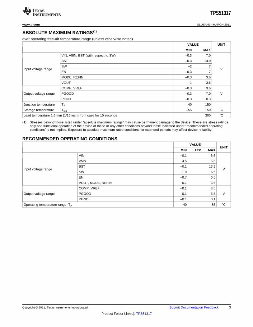
ABSOLUTE MAXIMUM RATINGS (1)
over operating free-air temperature range (unless otherwise noted)
VALUE UNIT
MIN MAX
VIN, V5IN, BST (with respect to SW) –0.3 7.0
BST –0.3 14.0
SW –2 7Input voltage range V
EN –0.3 7
MODE, REFIN –0.3 3.6
VOUT –1 3.6
COMP, VREF –0.3 3.6
Output voltage range PGOOD –0.3 7.0 V
PGND –0.3 0.3
Junction temperature TJ –40 150
Storage temperature Tstg –55 150 ˚CLead temperature 1,6 mm (1/16 inch) from case for 10 seconds 300 ˚C
(1) Stresses beyond those listed under “absolute maximum ratings” may cause permanent damage to the device. These are stress ratingsonly and functional operation of the device at these or any other conditions beyond those indicated under “recommended operatingconditions” is not implied. Exposure to absolute-maximum-rated conditions for extended periods may affect device reliability.
RECOMMENDED OPERATING CONDITIONSVALUE
UNITMIN TYP MAX
VIN –0.1 6.5
V5IN 4.5 6.5
BST –0.1 13.5Input voltage range V
SW –1.0 6.5
EN –0.7 6.5
VOUT, MODE, REFIN –0.1 3.5
COMP, VREF –0.1 3.5
Output voltage range PGOOD –0.1 5.5 V
PGND –0.1 0.1
Operating temperature range, TA -40 85 °C
Copyright © 2011, Texas Instruments Incorporated Submit Documentation Feedback 3
Product Folder Link(s): TPS51317

TPS51317
SLUSAH9 –MARCH 2011 www.ti.com
ELECTRICAL CHARACTERISTICSover recommended free-air temperature range, VV5IN = 5.0 V, PGND = GND (unless otherwise noted)
PARAMETER CONDITIONS MIN TYP MAX UNIT
SUPPLY: VOLTAGE, CURRENTS AND 5 V UVLO
IVINSD VIN shutdown current EN = 'LO' 0.02 5 µA
V5VIN 5VIN supply voltage V5IN voltage range 4.5 5.0 6.5 V
I5VIN 5VIN supply current EN =’HI’, V5IN supply current 1.1 2 mA
I5VINSD 5VIN shutdown current EN = ‘LO’, V5IN shutdown current 0.2 7.0 µA
VV5UVLO V5IN UVLO Ramp up; EN = 'HI' 4.20 4.37 4.50 V
VV5UVHYS V5IN UVLO hysteresis Falling hysteresis 440 mV
VVREFUVLO REF UVLO (1) Rising edge of VREF, EN = 'HI' 1.8 V
VVREFUVHYS REF UVLO hysteresis (1) 100 mV
VPOR5VFILT Reset OVP latch is reset by V5IN falling below the reset threshold 1.5 2.3 3.1 V
VOLTAGE FEEDBACK LOOP: VREF, VOUT, AND VOLTAGE GM AMPLIFIER
VOUTTOL VOUT accuracy VREFIN = 1 V, No droop –1% 0% 1%
IVREF = 0 µA 1.98 2.00 2.02VVREF VREF V
IVREF = 50 µA 1.975 2.000 2.025
IREFSNK VREF sink current VVREF = 2.05 V 2.5 mA
GM Transconductance 1.00 mS
VCM Common mode input voltage range (1) 0 2 V
VDM Differential mode input voltage 0 80 mV
ICOMPSNK COMP pin maximum sinking current VCOMP = 2 V, (VREFIN - VOUT) = 80 mV 80 µA
ICOMPSRC COMP pin maximum sourcing current VCOMP = 2 V -80 µA
VOFFSET Input offset voltage TA = 25°C 0 mV
RDSCH Output voltage discharge resistance 42 Ω
f–3dbVL –3dB Frequency (1) 4.5 6.0 7.5 MHz
CURRENT SENSE: CURRENT SENSE AMPLIFIER, OVERCURRENT AND ZERO CROSSING
Gain from the current of the low-side FET to PWM comparatorACSINT Internal current sense gain 43 53 57 mV/Awhen PWM = "OFF"
IOCL Positive overcurrent limit (valley) 7.6 A
IOCL(neg) Negative overcurrent limit (valley) –9.3 A
VZXOFF Zero crossing comp internal offset 0 mV
DRIVERS: BOOT STRAP SWITCH
RDSONBST Internal BST switch on-resistance IBST = 10 mA, TA = 25°C 10 Ω
IBSTLK Internal BST switch leakage current VBST = 14 V, VSW = 7 V 1 µA
PROTECTION: OVP, UVP, PGOOD, and THERMAL SHUTDOWN
PGOOD deassert to lowerVPGDLL Measured at the VOUT pin wrt/ VREFIN 84%(PGOOD → Low)
VPGHYSHL PGOOD high hysteresis 8%
PGOOD de-assert to higherVPGDLH Measured at the VOUT pin wrt/ VREFIN 116%(PGOOD → Low)
VPGHYSHH PGOOD high hysteresis -8%
Minimum VIN voltage for valid Measured at the VIN pin with a 2-mA sink current on PGOODVINMINPG 0.9 1.3 1.5 VPGOOD pin
VOVP OVP threshold Measured at the VOUT pin wrt/ VREFIN 117% 120% 123%
Measured at the VOUT pin wrt/ VREFIN, device latches OFF,VUVP UVP threshold 65% 68% 71%begins soft-stop
THSD Thermal shutdown (1) Latch off controller, attempt soft-stop. 145 °C
THSD(hys) Thermal Shutdown hysteresis (1) Controller re-starts after temperature has dropped 10 °C
(1) Ensured by design, not production tested.
4 Submit Documentation Feedback Copyright © 2011, Texas Instruments Incorporated
Product Folder Link(s): TPS51317

TPS51317
www.ti.com SLUSAH9 –MARCH 2011
ELECTRICAL CHARACTERISTICS (continued)over recommended free-air temperature range, VV5IN = 5.0 V, PGND = GND (unless otherwise noted)
PARAMETER CONDITIONS MIN TYP MAX UNIT
TIMERS: ON-TIME, MINIMUM OFF-TIME, SS, AND I/O TIMINGS
VVIN = 5 V, VVOUT = 1.05 V, fSW = 860 KHz 240
VVIN = 5 V, VVOUT = 1.05 V, fSW = 1 MHz 210tONESHOTC PWM one-shot (2) ns
VVIN = 5 V, VVOUT = 1.05 V, fSW = 1.2 MHz 175
VVIN = 5 V, VVOUT = 1.05 V, fSW = 1.5 MHz 140
VVIN = 5 V, VVOUT = 1.05 V, fSW = 1 MHz, DRVL on, SW =tMIN(off) Minimum OFF time 360 nsPGND, VVOUT < VREFIN
tINT(SS) Soft-start time From EN = HI to VOUT =95%, default setting 1.6 ms
tINT(SSDLY) Internal soft-start delay time From EN = HI to VOUT ramp starts 260 µs
tPGDDLY PGOOD startup delay time External tracking 8 ms
tPGDPDLYH PGOOD high propagation delay time 50 mV over drive, rising edge 0.8 1 1.2 ms
tPGDPDLYL PGOOD low propagation delay time 50 mV over drive, falling edge 10 µs
tOVPDLY OVP delay time Time from the VOUT pin out of +20% of REFIN to OVP fault 10 µs
Time from EN_INT going high to undervoltage fault is ready 2tUVDLYEN Undervoltage fault enable delay ms
External tracking from VOUT ramp starts 8
tUVPDLY UVP delay time Time from the VOUT pin out of –30% of REFIN to UVP fault 256 µs
LOGIC PINS: I/O VOLTAGE AND CURRENT
VPGDPD PGOOD pull-down voltage PGOOD low impedance, ISINK = 4 mA, VV5IN = 4.5 V 0.3 V
IPGDLKG PGOOD leakage current PGOOD high impedance, forced to 5.5 V –1 0 1 µA
VENH EN logic high EN, VCCP logic 2 V
VENL EN logic low EN, VCCP logic 0.5 V
IEN EN input current 1 µA
Threshold 1 80 130 180
Threshold 2 200 250 300 mVVMODETH MODE threshold voltage (3)
Threshold 3 370 420 470
Threshold 4 1.77 1.80 1.85 V
IMODE MODE current 15 µA
(2) Ensured by design, not production tested.(3) See Table 4 for descriptions of MODE parameters.
Copyright © 2011, Texas Instruments Incorporated Submit Documentation Feedback 5
Product Folder Link(s): TPS51317

VIN
VIN
PGND
PGND
SW
SW
SW
SW
V5IN
PG
OO
D
MO
DE
EN
6 7 8 9
11
12
13
14
15
BS
T
10
PGND SW
GN
D
VR
EF
CO
MP
RE
FIN
20 19 18 17
VO
UT
16
2
1
5
4
3
TPS51317
SLUSAH9 –MARCH 2011 www.ti.com
TPS51317RGB PACKAGE
(Top View)
Table 2. PIN FUNCTIONS
PINI/O DESCRIPTION
NO. NAME
Power supply for internal high-side gate driver. Connect a 0.1-µF bootstrap capacitor between this pin and16 BST I the SW pin.
8 COMP O Connect series R-C filter between this pin and VREF for loop compensation.
17 EN I Enable of the SMPS (3.3-V logic compatible).
6 GND – Signal ground.
18 MODE I Allows selection of switching frequencies light-load modes. (See Table 4)
1
2 PGND I Power ground. Source terminal of the rectifying low-side power FET. Positive input for current sensing.
3
19 PGOOD O Power good output. Connect pull-up resistor.
9 REFIN Target output voltageinput pin. Apply voltage between 0.6 V to 2.0 V.
11
12
13 SW I/O Switching node output. Connect to the external inductor. Also serve as current-sensing negative input.
14
15
20 V5IN I 5-V power supply for analog circuits and gate drive.
4VIN I Power supply input pin. Drain terminal of the switching high-side power FET.
5
10 VOUT I Output voltage monitor input pin.
7 VREF O 2.0-V reference output. Connect a 0.22-µF ceramic capacitor to GND.
6 Submit Documentation Feedback Copyright © 2011, Texas Instruments Incorporated
Product Folder Link(s): TPS51317

1
11
PGND
SW
TPS51317
OC
ZC
XCON
16 BST
18 V5IN
PWM
10
19 PGOOD
Control Logic
UDG-11058
+
+
VREFIN
+20%
+
+
VOUT
+
tON
One-
Shot
UV
OV
VREFIN
–30%
+8 R
8COMP
R
6GND
7VREF
On-Time
Selection
15 mA
18 MODE
VREFIN
16 %
VREFIN
16 %
+
+
Discharge
UVP
OVP
Current
Sense
+
VS
Smplifier
Current Sense
Amplifier
SW
PGND
4
5
VIN
VIN
12 SW
13 SW
14 SW
15 SW
2 PGND
3 PGND
17EN
Delay
� On/Off Time
� Minimum On/Off
� SKIP/RR (OTP)
� OCL/OVP/UVP
� DIsharge
+9REFIN
SSRamp
Comp
VBG
ZC Threshold
Modulation
PGND
GND
TPS51317
www.ti.com SLUSAH9 –MARCH 2011
BLOCK DIAGRAM
Copyright © 2011, Texas Instruments Incorporated Submit Documentation Feedback 7
Product Folder Link(s): TPS51317

TPS51317
1
2
3
4
16
11
7 10
BST
SWPGND
VOUT
VIN
EN
VREF
5
20
REFIN
V5IN
19 18
6
MODE
GND
0.1 mF
0.42 mH
22 mF
PGOOD
VOUT
= 1.5 V
PGOOD
5VIN
UDG-11059
2.2 mF
PGND
PGND
VIN
9
EN
8
COMP
12
13
14
15
SW
SW
SW
SW
17
22 mF 22 mF 22 mF 22 mF 22 mF
300 kW
0.22 mF
5 kW
0.1 mF
10 mF10 mF10 mF
100 kW
100 kW3.3 nF
TPS51317
1
2
3
4
16
11
7 10
BST
SWPGND
VOUT
VIN
EN
VREF
5
20
REFIN
V5IN
19 18
6
MODE
GND
0.1 mF
0.42 mH
22 mF
PGOOD
VOUT
= 1.5 V
PGOOD
5VIN
UDG-11060
2.2 mF
PGND
PGND
VIN
9
EN
8
COMP
12
13
14
15
SW
SW
SW
SW
17
22 mF 22 mF 22 mF 22 mF 22 mF
300 kW
0.22 mF
5 kW
0.1 mF
10 mF10 mF10 mF
100 kW
100 kW
TPS51317
SLUSAH9 –MARCH 2011 www.ti.com
APPLICATION SCHEMATIC WITH TPS51317
Figure 1. Application Using Non-Droop Configuration
Figure 2. Application Using Droop Configuration
8 Submit Documentation Feedback Copyright © 2011, Texas Instruments Incorporated
Product Folder Link(s): TPS51317

TPS51317
www.ti.com SLUSAH9 –MARCH 2011
Application Circuit List of Materials
Recommended parts for key external components for the circuits in Figure 1 and Figure 2 are listed in Table 3.
Table 3. Key External Component Recommendations(Figure 1 and Figure 2)
FUNCTION MANUFACTURER PART NUMBER
Output Inductor Nec-Tokin MPCG0740LR42C
Panasonic ECJ2FB0J226MCeramic Output Capacitors
Murata GRM21BR60J226ME39L
Copyright © 2011, Texas Instruments Incorporated Submit Documentation Feedback 9
Product Folder Link(s): TPS51317

Time (ms)
Vo
ltag
e(V
)
Current
Feedback
tON
t
VCS
VCOMP
UDG-10187
VREF
TPS51317
SLUSAH9 –MARCH 2011 www.ti.com
APPLICATION INFORMATION
Functional Overview
The TPS51317 is a D-CAP+™ mode adaptive on-time converter. Integrated high-side and low-side FET supportsoutput current to a maximum of 6-ADC. The converter automatically runs in discontinuous conduction mode(DCM) to optimize light-load efficiency. Multiple switching frequencies are provided to enable optimization of thepower chain for the cost, size and efficiency requirements of the design (see Table 4).
In adaptive on-time converters, the controller varies the on-time as a function of input and output voltage tomaintain a nearly constant frequency during steady-state conditions. In conventional constant on-time converters,each cycle begins when the output voltage crosses to a fixed reference level. However, in the TPS51317, thecycle begins when the current feedback reaches an error voltage level which is the amplified difference betweenthe reference voltage and the feedback voltage.
PWM Operation
Referring to Figure 3, in steady state, continuous conduction mode, the converter operates in the following way.
Starting with the condition that the top FET is off and the bottom FET is on, the current feedback (VCS) is higherthan the error amplifier output (VCOMP). VCS falls until it hits VCOMP, which contains a component of the outputripple voltage. VCS is not directly accessible by measuring signals on pins of TPS51317. The PWM comparatorsenses where the two waveforms cross and triggers the on-time generator.
Figure 3. D-CAP+™ Mode Basic Waveforms
The current feedback is an amplified and filtered version of the voltage between PGND and SW during low-sideFET on-time. The TPS51317 also provides a single-ended differential voltage (VOUT) feedback to increase thesystem accuracy and reduce the dependence of circuit performance on layout.
10 Submit Documentation Feedback Copyright © 2011, Texas Instruments Incorporated
Product Folder Link(s): TPS51317

= ´OUT
ON
IN SW
V 1t
V f
+V
SLEW
+
–
RC
+ PWM
Comparator
RDS(on)
GMV
= 1 mS
Driver
LOUT
ESR
COUT
ROUT
UDG-10190
RLOAD
8 kW
+
–
+G
MC= 1 mS
CC
VREF
TPS51317
www.ti.com SLUSAH9 –MARCH 2011
PWM Frequency and Adaptive on Time Control
In general, the on-time (at the SW node) can be estimated by Equation 1.
where• fSW is the frequency selected by the connection of the MODE pin (1)
The on-time pulse is sent to the top FET. The inductor current and the current feedback rises to peak value.Each ON pulse is latched to prevent double pulsing. Switching frequency settings are shown in .
Non-Droop Configuration
The TPS51317 can be configured as a non-droop solution. The benefit of a non-droop approach is that loadregulation is flat, therefore, in a system where tight DC tolerance is desired, the non-droop approach isrecommended. For the Intel system agent application, non-droop is recommended as the standard configuration.
The non-droop approach can be implemented by connecting a resistor and a capacitor between the COMP andthe VREF pins. The purpose of the type II compensation is to obtain high DC feedback gain while minimizing thephase delay at unity gain cross over frequency of the converter.
The value of the resistor (RC) can be calculated using the desired unity gain bandwidth of the converter, and thevalue of the capacitor (CC) can be calculated by knowing where the zero location is desired. An application toolthat calculates these values is available from your local TI Field Application Engineer.
Figure 4 shows the basic implementation of the non-droop mode using the TPS51317.
Figure 4. Non-Droop Mode Basic Implementation
Figure 5 shows shows the load regulation using non-droop configuration.
Figure 6 shows the transient response of TPS51317 using non-droop configuration, where COUT = 6 x 22 µF. Theapplied step load is from 0 A to 3 A.
Copyright © 2011, Texas Instruments Incorporated Submit Documentation Feedback 11
Product Folder Link(s): TPS51317

1.350
1.375
1.400
1.425
1.450
1.475
1.500
1.525
1.550
1.575
1.600
1.625
1.650
0 1 2 3 4 5 6Output Current (A)
Out
put V
olta
ge (
V)
VIN = 5 V
´=
´
CSINTDROOP
DROOP M
A I(L)V
R G
= = \ =´ ´
DROOP CSINT CSINTLOAD _LINE DROOP
DROOP M LOAD _LINE M
V A AR R
I(L) R G R G
TPS51317
SLUSAH9 –MARCH 2011 www.ti.com
Figure 5. 1.5-V Load Regulation (VIN = 5 V) Figure 6. Non-Droop Configuration TransientNon-Droop Configuration Response
Droop Configuration
The terminology for droop is the same as load line or voltage positioning as defined in the Intel CPU VCOREspecification. Based on the actual tolerance requirement of the application, load-line set points can be defined tomaximize either cost savings (by reducing output capacitors) or power reduction benefits.
Accurate droop voltage response is provided by the finite gain of the droop amplifier. The equation for droopvoltage is shown in Equation 2.
where• low-side on-resistence is used as the current sensing element• ACSINT is a constant, which nominally is 53 mV/A.• I(L) is the DC current of the inductor, or the load current• RDROOP is the value of resistor from the COMP pin to the VREF pin• GM is the transconductance of the droop amplifier with nominal value of 1 mS (2)
Equation 3 can be used to easily derive RDROOP for any load line slope/droop design target.
(3)
12 Submit Documentation Feedback Copyright © 2011, Texas Instruments Incorporated
Product Folder Link(s): TPS51317

+V
SLEW
+
–
RDROOP
+ PWM
Comparator
RDS(on)
GMV
= 1 mS
Driver
LOUT
ESR
COUT
ROUT
UDG-10188
RLOAD
8 kW
+
–
+G
MC= 1 mS
VREF
UDG-11080
Droop
ILOAD
VOUT
setpoint at 0 A
Maximum undershoot voltage =(5%–1%) x 1 = 4% x VOUT
Load insertion
Load release
Non-
Droop
Maximum transient voltage
= (5%–1%) x 2 = 8% x VOUT
VOUT
setpoint at 6 A
VOUT
setpoint at 0 A
Maximum overshoot voltage =(5%–1%) x 1 = 4% x VOUT
TPS51317
www.ti.com SLUSAH9 –MARCH 2011
Figure 7 shows the basic implementation of the droop mode using the TPS51317.
Figure 7. DROOP Mode Basic Implementation
The droop (voltage positioning) method was originally recommended to reduce the number of external outputcapacitors required. The effective transient voltage range is increased because of the active voltage positioning(see Figure 8).
Figure 8. DROOP vs Non-DROOP in Transient Voltage Window
In applications where the DC and the AC tolerances are not separated, which means there is not a strict DCtolerance requirement, the droop method can be used.
Copyright © 2011, Texas Instruments Incorporated Submit Documentation Feedback 13
Product Folder Link(s): TPS51317
1.350
1.375
1.400
1.425
1.450
1.475
1.500
1.525
1.550
1.575
1.600
1.625
1.650
0 1 2 3 4 5 6Output Current (A)
Out
put V
olta
ge (
V)
VIN =3.3 V
TPS51317
SLUSAH9 –MARCH 2011 www.ti.com
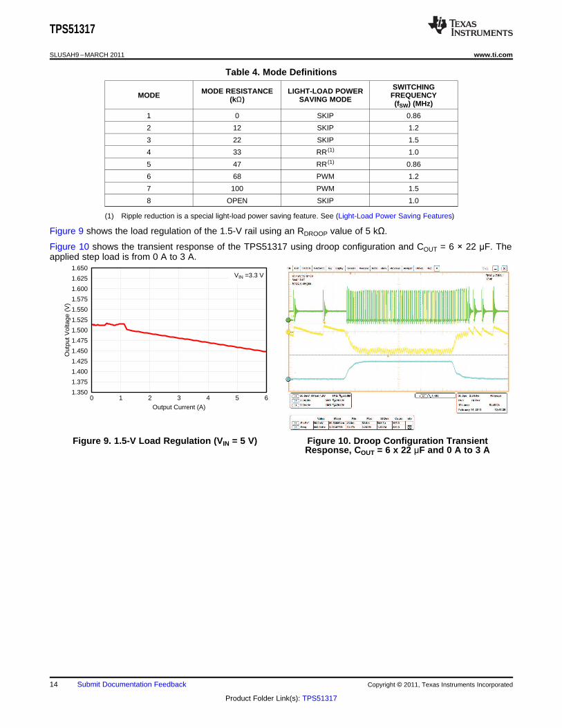
Table 4. Mode Definitions
SWITCHINGMODE RESISTANCE LIGHT-LOAD POWERMODE FREQUENCY(kΩ) SAVING MODE (fSW) (MHz)
1 0 SKIP 0.86
2 12 SKIP 1.2
3 22 SKIP 1.5
4 33 RR (1) 1.0
5 47 RR (1) 0.86
6 68 PWM 1.2
7 100 PWM 1.5
8 OPEN SKIP 1.0
(1) Ripple reduction is a special light-load power saving feature. See (Light-Load Power Saving Features)
Figure 9 shows the load regulation of the 1.5-V rail using an RDROOP value of 5 kΩ.
Figure 10 shows the transient response of the TPS51317 using droop configuration and COUT = 6 × 22 µF. Theapplied step load is from 0 A to 3 A.
Figure 9. 1.5-V Load Regulation (VIN = 5 V) Figure 10. Droop Configuration TransientResponse, COUT = 6 x 22 µF and 0 A to 3 A
14 Submit Documentation Feedback Copyright © 2011, Texas Instruments Incorporated
Product Folder Link(s): TPS51317

TPS51317
www.ti.com SLUSAH9 –MARCH 2011
Light-Load Power Saving Features
The TPS51317 has an automatic pulse-skipping mode to provide excellent efficiency over a wide load range.The converter senses inductor current and prevents negative flow by shutting off the low-side gate driver. Thissaves power by eliminating re-circulation of the inductor current. Further, when the bottom FET shuts off, theconverter enters discontinuous mode, and the switching frequency decreases, thus reducing switching losses aswell.
TPS51317 also provides a special light-load power saving feature, called ripple reduction. Essentially, it reducesthe on-time in SKIP mode to effectively reduce the output voltage ripple associated with using an all MLCCcapacitor output power stage design.
Power Sequences
Non-Tracking Startup
The TPS51317 can be configured for non-tracking application. When non-tracking is configured, output voltage isregulated to the REFIN voltage which taps off the voltage dividers from the 2VREF. Either the EN pin or the V5INpin can be used to start up the device. The TPS51317 uses internal voltage servo DAC to provide a precise1.6-ms soft-start time during soft-start initialization. (See Figure 11)
Tracking Startup
TPS51317 can also be configured for tracking application. When tracking configuration is desired, output voltageis also regulated to the REFIN voltage which comes from external power source. In order for TPS51317 todifferentiate between a non-tracking configuration or a tracking configuration, there is a minimum delay time of260 µs required between the time when the EN pin or the 5VIN pin is validated to the time when the REFIN pinvoltage can be applied, in order for the TPS51317 to track properly (see Figure 12). The valid REFIN voltagerange is between 0.6 V to 2 V.
Protection Features
The TPS51317 offers many features to protect the converter power chain as well as the system electronics.
5-V Undervoltage Protection (UVLO)
The TPS51317 continuously monitors the voltage on the V5IN pin to ensure that the voltage level is high enoughto bias the device properly and to provide sufficient gate drive potential to maintain high efficiency. The converterstarts with approximately 4.3 V and has a nominal of 440 mV of hysteresis. If the 5-V UVLO limit is reached, theconverter transitions the phase node into a off function. And the converter remains in the off state until the deviceis reset by cycling 5 V until the 5-V POR is reached (2.3-V nominal). The power input does not have an UVLOfunction
Power Good Signals
The TPS51317 has one open-drain power good (PGOOD) pin. During startup, there is a 1-ms power good highpropagation delay. The PGOOD pin de-asserts as soon as the EN pin is pulled low or an undervoltage conditionon V5IN or any other faults that require latch off action is detected.
Output Overvoltage Protection (OVP)
In addition to the power good function described above, the TPS51317 has additional OVP and UVP thresholdsand protection circuits.
An OVP condition is detected when the output voltage is approximately 120% × VREFIN. In this case, theconverter de-asserts the PGOOD signals and performs the overvoltage protection function. The converterremains in this state until the device is reset by cycling 5 V until the 5-V POR threshold (2.3 V nominal) isreached.
Output Undervoltage Protection (UVP)
Output undervoltage protection works in conjunction with the current protection described in the OvercurrentProtection and Overcurrent Limit sections. If the output voltage drops below 70% of VREFIN, after an 8-µs delay,the device latches OFF. Undervoltage protection can be reset only by EN or a 5-V POR.
Copyright © 2011, Texas Instruments Incorporated Submit Documentation Feedback 15
Product Folder Link(s): TPS51317

( ) ( ) -= + ´ P POCL dc OCL valley
1I I I
2
TPS51317
SLUSAH9 –MARCH 2011 www.ti.com
Overcurrent Protection
Both positive and negative overcurrent protection are provided in the TPS51317:• Overcurrent Limit (OCL)• Negative OCL (level same as positive OCL)
Overcurrent Limit
If the sensed current value is above the OCL setting, the converter delays the next ON pulse until the currentdrops below the OCL limit. Current limiting occurs on a pulse-by-pulse basis. The TPS51317 uses a valleycurrent limiting scheme where the DC OCL trip point is the OCL limit plus half of the inductor ripple current. Theminimum valley OCL is 6 A over process and temperature.
During the overcurrent protection event, the output voltage likely droops until the UVP limit is reached. Then, theconverter de-asserts the PGOOD pin, and then latches OFF after an 8-µs delay. The converter remains in thisstate until the device is reset.
(4)
Negative OCL
The negative OCL circuit acts when the converter is sinking current from the output capacitor(s). The convertercontinues to act in a valley mode, the absolute value of the negative OCL set point is typically -6.5 A.
Thermal Protection
Thermal Shutdown
The TPS51317 has an internal temperature sensor. When the temperature reaches a nominal 145°C, the deviceshuts down until the temperature cools by approximately 10°C. Then the converter restarts.
16 Submit Documentation Feedback Copyright © 2011, Texas Instruments Incorporated
Product Folder Link(s): TPS51317

TPS51317
www.ti.com SLUSAH9 –MARCH 2011
Startup Timing Diagrams
Figure 11. Non-Tracking Start-Up
Figure 12. Tracking Start-Up
Copyright © 2011, Texas Instruments Incorporated Submit Documentation Feedback 17
Product Folder Link(s): TPS51317

40
45
50
55
60
65
70
75
80
85
90
95
0.01 0.1 1 10Output Current (A)
Effi
cien
cy (
%)
Mode 1Mode 3Mode 4Mode 7Mode 8
TA = 25°CVIN = 3.3 V
40
45
50
55
60
65
70
75
80
85
90
95
0.01 0.1 1 10Output Current (A)
Effi
cien
cy (
%)
Mode 1Mode 3Mode 4Mode 7Mode 8
TA = 25°CVIN = 5 V
0.00
0.25
0.50
0.75
1.00
1.25
1.50
0.1 1 10Output Current (A)
Pow
er L
oss
(W)
Mode 1Mode 3Mode 4Mode 7Mode 8
TA = 25°CVIN = 3.3 V
0.00
0.25
0.50
0.75
1.00
1.25
1.50
0.1 1 10Output Current (A)
Pow
er L
oss
(W)
Mode 1Mode 3Mode 4Mode 7Mode 8
TA = 25°CVIN = 5 V
100
150
200
250
300
350
400
50
0
-30
-20
-10
30
40
50
-40
-50
0
10
20
Frequency (Hz)
Gain
Phase
1000 10 k 100 k 1 M 10 M
Gain
(dB
)
Phase
(°)
25°C
-10°C
85°C
60
110
160
210
260
310
360
10
-40
-30
-20
-10
30
40
50
-40
-50
0
10
20
Frequency (Hz)
Gain
Phase
25°C
-10°C
85°C
1000 10 k 100 k 1 M 10 M
Gain
(dB
)
Phase
(°)
60
TPS51317
SLUSAH9 –MARCH 2011 www.ti.com
TYPICAL CHARACTERISTICS
Figure 13. Efficiency vs Output Current Figure 14. Efficiency vs Output Current
Figure 15. Power Loss Figure 16. Power Loss
Figure 17. Bode Plot (Non-Droop Mode) VIN = 5 V, Figure 18. Bode Plot (Droop Mode), VIN = 5 V,VOUT = 0.8 V, ILOAD = 5 A VOUT = 0.8 V, ILOAD = 5 A
18 Submit Documentation Feedback Copyright © 2011, Texas Instruments Incorporated
Product Folder Link(s): TPS51317

-= ´ =P PI 6 A 0.4 2.4 A
( )( )
( )( )
- -
æ ö æ ö- ´ - ´ç ÷ ç ÷
ç ÷ ç ÷´ ´´ è ø è ø= = = = m
OUTIN OUT
SW IN
P P P P
V 1.5V V 5 1.5
f V 1 5V dTL 0.43 H
I I 1.5 A
= ´+
VREFOUT LOWER
UPPER LOWER
VV R
R R
( ) ( ) -= + ´ = + ´ =P POCL dc OCL valley
1 1I I I 6 A 1.5 A 6.75 A
2 2
TPS51317
www.ti.com SLUSAH9 –MARCH 2011
DESIGN PROCEDURE
The simplified design procedure is done for a non-droop application using the TPS51317 converter.
Step One
Determine the specifications.
The Rail requirements provide the following key parameters:1. VOUT = 1.5 V2. ICC(max) = 6 A3. IDYN(max) = 3 A4. ICC(tdc) = 3 A
Step Two
Determine system parameters.
The input voltage range and operating frequency are of primary interest. For example:1. VIN = 5 V2. fSW = 1 MHz
Step Three
Determine inductor value and choose inductor.
Smaller values of inductor have better transient performance but higher ripple and lower efficiency. Higher valueshave the opposite characteristics. It is common practice to limit the ripple current to 25% to 50% of the maximumcurrent. In this case, use 40%:
(5)
At fSW = 1 MHz, with a 5-V input and a 1.5-V output:
(6)
For this application, a 0.42-µH, 1.55-mΩ inductor from NEC-TOKIN with part number MPCG0740LR42C ischosen.
Step Four
Set the output voltage.
(7)
The output voltage is determined by the 2-V reference (VREF) and the resistor dividers (RUPPER and RLOWER).The output voltage is regulated to the REFIN pin. Because the 2-V reference current capability is limited to lessthan 50 µA, care should be taken when selecting the resistor dividers. For the current reference design of 1.5 V(see application schematics shown in Figure 1 and Figure 2, RUPPER = 100 kΩ, RLOWER = 300 kΩ.
Step Five
Calculate OCL.
The DC OCL level of TPS51317 design is determined by Equation 8,
(8)
Copyright © 2011, Texas Instruments Incorporated Submit Documentation Feedback 19
Product Folder Link(s): TPS51317

( )
( )( )
( )
( )
( )
( )( )
æ ö´
ç ÷´ D ´ +ç ÷è ø
=æ öæ ö-ç ÷ç ÷´ D ´ ´ - ´ç ÷ç ÷è øè ø
2 VOUT SWLOAD max MIN off
IN min
OUT min_under
VOUTIN min
SW VOUTLOAD insert MIN off
IN min
V tL I t
V
C
V V
2 V t t VV
( )
( )( )
( )
´ D
=´ D ´
2
OUT LOAD max
OUT min_ overVOUTLOAD release
L I
C2 V V
= ´ ´ =p
CM0
OUT S
RG1f 190kHz
2 C R
´ ´ p ´ ´ W ´ p ´ m= = » W
0 S OUTC
M
f R 2 C 190kHz 53m 2 80 FR 5k
G 1mS
=p ´ ´
=0
Z
C C
f1f
2 R C 10
TPS51317
SLUSAH9 –MARCH 2011 www.ti.com
The minimum valley OCL is 6 A over process and temperature, and IP-P = 1.5 A, the minimum DC OCL iscalculated to be 6.75A.
Step Six
Determine the output capacitance.
To determine COUT based on transient and stability requirement, first calculate the the minimum outputcapacitance for a given transient.
Equation 10 and Equation 9 can be used to estimate the amount of capacitance needed for a given dynamic loadstep/release. Please note that there are other factors that may impact the amount of output capacitance for aspecific design, such as ripple and stability. Equation 10 and Equation 9 are used only to estimate the transientrequirement, the result should be used in conjunction with other factors of the design to determine the necessaryoutput capacitance for the application.
(9)
(10)
Equation 9 and Equation 10 calculate the minimum COUT for meeting the transient requirement, which is 84 µFassuming the following:• ±3% voltage allowance for load step and release• MLCC capacitance derating of 60% due to DC and AC bias effect
In this reference design, 6, 22-µF capacitors are used in order to provide this amount of capacitance.
Step Seven
Determine the stability based on the output capacitance COUT.
In order to achieve stable operation. The 0-dB frequency, f0 should be kept less than 1/5 of the switchingfrequency (1 MHz). (See Figure 4)
where• RS = RDS(on) × GMC × RLOAD (11)
.
(12)
Using 6, 22-µF capacitors, the compensation resistance, RC can be calculated to be approximately 5 kΩ.
The purpose of the comparator capacitor (CC) is to reduce the DC component to obtain high DC feedback gain.However, as it causes phase delay, another zero to cancel this effect at f0 is needed. This zero can bedetermined by values of CC and the compensation resistor, RC.
(13)
And since RC has previously been derived, the value of CC is calculated to be 2.2 nF. In order to further boostphase margin, a value of 3.3-nF is chosen for this reference design.
20 Submit Documentation Feedback Copyright © 2011, Texas Instruments Incorporated
Product Folder Link(s): TPS51317

TPS51317
www.ti.com SLUSAH9 –MARCH 2011
Step Eight
Select decoupling and peripheral components.
For TPS51317 peripheral capacitors use the following minimum values of ceramic capacitance. X5R or bettertemperature coefficient is recommended. Tighter tolerances and higher voltage ratings are always appropriate.• V5IN decoupling ≥ 22 µF, ≥ 10 V• VREF decoupling 0.22 µF to 1 µF, ≥ 4 V• Bootstrap capacitors ≥ 0.1 µF, ≥ 10 V• Pull-up resistors on PGOOD, 100 kΩ
Layout Considerations
Good layout is essential for stable power supply operation. Follow these guidelines for an efficient PCB layout.• Connect PGND pins (or at least one of the pins) to the thermal PAD underneath the device. Also connect
GND pin to the thermal PAD underneath the device. Use four vias to connect the thermal pad to internalground planes.
• Place VIN, V5IN and 2VREF decoupling capacitors as close to the device as possible.• Use wide traces for the VIN, VOUT, PGND and SW pins. These nodes carry high current and also serve as
heat sinks.• Place feedback and compensation components as close to the device as possible.• Keep COMP analog signal away from noisy signals (SW, BST).
Copyright © 2011, Texas Instruments Incorporated Submit Documentation Feedback 21
Product Folder Link(s): TPS51317

PACKAGE OPTION ADDENDUM
www.ti.com 11-Apr-2013
Addendum-Page 1
PACKAGING INFORMATION
Orderable Device Status(1)
Package Type PackageDrawing
Pins PackageQty
Eco Plan(2)
Lead/Ball Finish MSL Peak Temp(3)
Op Temp (°C) Top-Side Markings(4)
Samples
TPS51317RGBR ACTIVE VQFN RGB 20 3000 Green (RoHS& no Sb/Br)
CU NIPDAU Level-2-260C-1 YEAR -40 to 85 51317
TPS51317RGBT ACTIVE VQFN RGB 20 250 Green (RoHS& no Sb/Br)
CU NIPDAU Level-2-260C-1 YEAR -40 to 85 51317
(1) The marketing status values are defined as follows:ACTIVE: Product device recommended for new designs.LIFEBUY: TI has announced that the device will be discontinued, and a lifetime-buy period is in effect.NRND: Not recommended for new designs. Device is in production to support existing customers, but TI does not recommend using this part in a new design.PREVIEW: Device has been announced but is not in production. Samples may or may not be available.OBSOLETE: TI has discontinued the production of the device.
(2) Eco Plan - The planned eco-friendly classification: Pb-Free (RoHS), Pb-Free (RoHS Exempt), or Green (RoHS & no Sb/Br) - please check http://www.ti.com/productcontent for the latest availabilityinformation and additional product content details.TBD: The Pb-Free/Green conversion plan has not been defined.Pb-Free (RoHS): TI's terms "Lead-Free" or "Pb-Free" mean semiconductor products that are compatible with the current RoHS requirements for all 6 substances, including the requirement thatlead not exceed 0.1% by weight in homogeneous materials. Where designed to be soldered at high temperatures, TI Pb-Free products are suitable for use in specified lead-free processes.Pb-Free (RoHS Exempt): This component has a RoHS exemption for either 1) lead-based flip-chip solder bumps used between the die and package, or 2) lead-based die adhesive used betweenthe die and leadframe. The component is otherwise considered Pb-Free (RoHS compatible) as defined above.Green (RoHS & no Sb/Br): TI defines "Green" to mean Pb-Free (RoHS compatible), and free of Bromine (Br) and Antimony (Sb) based flame retardants (Br or Sb do not exceed 0.1% by weightin homogeneous material)
(3) MSL, Peak Temp. -- The Moisture Sensitivity Level rating according to the JEDEC industry standard classifications, and peak solder temperature.
(4) Multiple Top-Side Markings will be inside parentheses. Only one Top-Side Marking contained in parentheses and separated by a "~" will appear on a device. If a line is indented then it is acontinuation of the previous line and the two combined represent the entire Top-Side Marking for that device.
Important Information and Disclaimer:The information provided on this page represents TI's knowledge and belief as of the date that it is provided. TI bases its knowledge and belief on informationprovided by third parties, and makes no representation or warranty as to the accuracy of such information. Efforts are underway to better integrate information from third parties. TI has taken andcontinues to take reasonable steps to provide representative and accurate information but may not have conducted destructive testing or chemical analysis on incoming materials and chemicals.TI and TI suppliers consider certain information to be proprietary, and thus CAS numbers and other limited information may not be available for release.
In no event shall TI's liability arising out of such information exceed the total purchase price of the TI part(s) at issue in this document sold by TI to Customer on an annual basis.

TAPE AND REEL INFORMATION
*All dimensions are nominal
Device PackageType
PackageDrawing
Pins SPQ ReelDiameter
(mm)
ReelWidth
W1 (mm)
A0(mm)
B0(mm)
K0(mm)
P1(mm)
W(mm)
Pin1Quadrant
TPS51317RGBR VQFN RGB 20 3000 330.0 12.4 3.8 4.3 1.5 8.0 12.0 Q1
TPS51317RGBR VQFN RGB 20 3000 330.0 12.4 3.8 4.3 1.5 8.0 12.0 Q1
TPS51317RGBT VQFN RGB 20 250 180.0 12.4 3.8 4.3 1.5 8.0 12.0 Q1
TPS51317RGBT VQFN RGB 20 250 180.0 12.4 3.8 4.3 1.5 8.0 12.0 Q1
PACKAGE MATERIALS INFORMATION
www.ti.com 26-Jan-2013
Pack Materials-Page 1

*All dimensions are nominal
Device Package Type Package Drawing Pins SPQ Length (mm) Width (mm) Height (mm)
TPS51317RGBR VQFN RGB 20 3000 367.0 367.0 35.0
TPS51317RGBR VQFN RGB 20 3000 367.0 367.0 35.0
TPS51317RGBT VQFN RGB 20 250 210.0 185.0 35.0
TPS51317RGBT VQFN RGB 20 250 210.0 185.0 35.0
PACKAGE MATERIALS INFORMATION
www.ti.com 26-Jan-2013
Pack Materials-Page 2


IMPORTANT NOTICE
Texas Instruments Incorporated and its subsidiaries (TI) reserve the right to make corrections, enhancements, improvements and otherchanges to its semiconductor products and services per JESD46, latest issue, and to discontinue any product or service per JESD48, latestissue. Buyers should obtain the latest relevant information before placing orders and should verify that such information is current andcomplete. All semiconductor products (also referred to herein as “components”) are sold subject to TI’s terms and conditions of salesupplied at the time of order acknowledgment.TI warrants performance of its components to the specifications applicable at the time of sale, in accordance with the warranty in TI’s termsand conditions of sale of semiconductor products. Testing and other quality control techniques are used to the extent TI deems necessaryto support this warranty. Except where mandated by applicable law, testing of all parameters of each component is not necessarilyperformed.TI assumes no liability for applications assistance or the design of Buyers’ products. Buyers are responsible for their products andapplications using TI components. To minimize the risks associated with Buyers’ products and applications, Buyers should provideadequate design and operating safeguards.TI does not warrant or represent that any license, either express or implied, is granted under any patent right, copyright, mask work right, orother intellectual property right relating to any combination, machine, or process in which TI components or services are used. Informationpublished by TI regarding third-party products or services does not constitute a license to use such products or services or a warranty orendorsement thereof. Use of such information may require a license from a third party under the patents or other intellectual property of thethird party, or a license from TI under the patents or other intellectual property of TI.Reproduction of significant portions of TI information in TI data books or data sheets is permissible only if reproduction is without alterationand is accompanied by all associated warranties, conditions, limitations, and notices. TI is not responsible or liable for such altereddocumentation. Information of third parties may be subject to additional restrictions.Resale of TI components or services with statements different from or beyond the parameters stated by TI for that component or servicevoids all express and any implied warranties for the associated TI component or service and is an unfair and deceptive business practice.TI is not responsible or liable for any such statements.Buyer acknowledges and agrees that it is solely responsible for compliance with all legal, regulatory and safety-related requirementsconcerning its products, and any use of TI components in its applications, notwithstanding any applications-related information or supportthat may be provided by TI. Buyer represents and agrees that it has all the necessary expertise to create and implement safeguards whichanticipate dangerous consequences of failures, monitor failures and their consequences, lessen the likelihood of failures that might causeharm and take appropriate remedial actions. Buyer will fully indemnify TI and its representatives against any damages arising out of the useof any TI components in safety-critical applications.In some cases, TI components may be promoted specifically to facilitate safety-related applications. With such components, TI’s goal is tohelp enable customers to design and create their own end-product solutions that meet applicable functional safety standards andrequirements. Nonetheless, such components are subject to these terms.No TI components are authorized for use in FDA Class III (or similar life-critical medical equipment) unless authorized officers of the partieshave executed a special agreement specifically governing such use.Only those TI components which TI has specifically designated as military grade or “enhanced plastic” are designed and intended for use inmilitary/aerospace applications or environments. Buyer acknowledges and agrees that any military or aerospace use of TI componentswhich have not been so designated is solely at the Buyer's risk, and that Buyer is solely responsible for compliance with all legal andregulatory requirements in connection with such use.TI has specifically designated certain components as meeting ISO/TS16949 requirements, mainly for automotive use. In any case of use ofnon-designated products, TI will not be responsible for any failure to meet ISO/TS16949.
Products ApplicationsAudio www.ti.com/audio Automotive and Transportation www.ti.com/automotiveAmplifiers amplifier.ti.com Communications and Telecom www.ti.com/communicationsData Converters dataconverter.ti.com Computers and Peripherals www.ti.com/computersDLP® Products www.dlp.com Consumer Electronics www.ti.com/consumer-appsDSP dsp.ti.com Energy and Lighting www.ti.com/energyClocks and Timers www.ti.com/clocks Industrial www.ti.com/industrialInterface interface.ti.com Medical www.ti.com/medicalLogic logic.ti.com Security www.ti.com/securityPower Mgmt power.ti.com Space, Avionics and Defense www.ti.com/space-avionics-defenseMicrocontrollers microcontroller.ti.com Video and Imaging www.ti.com/videoRFID www.ti-rfid.comOMAP Applications Processors www.ti.com/omap TI E2E Community e2e.ti.comWireless Connectivity www.ti.com/wirelessconnectivity
Mailing Address: Texas Instruments, Post Office Box 655303, Dallas, Texas 75265Copyright © 2016, Texas Instruments Incorporated