32 mbit (4mb x8 or 2mb x16, dual bank 16:16, boot block
TRANSCRIPT

1/50March 2008
M29DW324DTM29DW324DB
32 Mbit (4Mb x8 or 2Mb x16, Dual Bank 16:16, Boot Block)3V Supply Flash Memory
FEATURES SUMMARY■ SUPPLY VOLTAGE
– VCC = 2.7V to 3.6V for Program, Erase and Read
– VPP =12V for Fast Program (optional)■ ACCESS TIME: 70, 90ns■ PROGRAMMING TIME
– 10µs per Byte/Word typical– Double Word/ Quadruple Byte Program
■ MEMORY BLOCKS– Dual Bank Memory Array: 16Mbit+16Mbit– Parameter Blocks (Top or Bottom
Location)■ DUAL OPERATIONS
– Read in one bank while Program or Erase in other
■ ERASE SUSPEND and RESUME MODES– Read and Program another Block during
Erase Suspend■ UNLOCK BYPASS PROGRAM COMMAND
– Faster Production/Batch Programming■ VPP/WP PIN for FAST PROGRAM and
WRITE PROTECT■ TEMPORARY BLOCK UNPROTECTION
MODE■ COMMON FLASH INTERFACE
– 64 bit Security Code■ EXTENDED MEMORY BLOCK
– Extra block used as security block or to store additional information
■ LOW POWER CONSUMPTION– Standby and Automatic Standby
■ 100,000 PROGRAM/ERASE CYCLES per BLOCK
■ ELECTRONIC SIGNATURE– Manufacturer Code: 0020h– Top Device Code M29DW324DT: 225Ch– Bottom Device Code M29DW324DB:
225Dh
Figure 1. Packages
TSOP48 (N)12 x 20mm
FBGA
TFBGA48 (ZE)6 x 8mm

M29DW324DT, M29DW324DB
2/50
TABLE OF CONTENTS
FEATURES SUMMARY . . . . . . . . . . . . . . . . . . . . . . . . . . . . . . . . . . . . . . . . . . . . . . . . . . . . . . . . . . . . . 1
Figure 1. Packages. . . . . . . . . . . . . . . . . . . . . . . . . . . . . . . . . . . . . . . . . . . . . . . . . . . . . . . . . . . . . . 1
SUMMARY DESCRIPTION. . . . . . . . . . . . . . . . . . . . . . . . . . . . . . . . . . . . . . . . . . . . . . . . . . . . . . . . . . . 5
Figure 2. Logic Diagram . . . . . . . . . . . . . . . . . . . . . . . . . . . . . . . . . . . . . . . . . . . . . . . . . . . . . . . . . . 5Table 1. Signal Names . . . . . . . . . . . . . . . . . . . . . . . . . . . . . . . . . . . . . . . . . . . . . . . . . . . . . . . . . . 5Figure 3. TSOP Connections . . . . . . . . . . . . . . . . . . . . . . . . . . . . . . . . . . . . . . . . . . . . . . . . . . . . . . 6Figure 4. TFBGA48 Connections (Top view through package) . . . . . . . . . . . . . . . . . . . . . . . . . . . . 7Table 2. Bank Architecture . . . . . . . . . . . . . . . . . . . . . . . . . . . . . . . . . . . . . . . . . . . . . . . . . . . . . . . 7Figure 5. Block Addresses (x8). . . . . . . . . . . . . . . . . . . . . . . . . . . . . . . . . . . . . . . . . . . . . . . . . . . . . 8Figure 6. Block Addresses (x16). . . . . . . . . . . . . . . . . . . . . . . . . . . . . . . . . . . . . . . . . . . . . . . . . . . . 9
SIGNAL DESCRIPTIONS . . . . . . . . . . . . . . . . . . . . . . . . . . . . . . . . . . . . . . . . . . . . . . . . . . . . . . . . . . . 10
Address Inputs (A0-A20). . . . . . . . . . . . . . . . . . . . . . . . . . . . . . . . . . . . . . . . . . . . . . . . . . . . . . . . . 10Data Inputs/Outputs (DQ0-DQ7). . . . . . . . . . . . . . . . . . . . . . . . . . . . . . . . . . . . . . . . . . . . . . . . . . . 10Data Inputs/Outputs (DQ8-DQ14). . . . . . . . . . . . . . . . . . . . . . . . . . . . . . . . . . . . . . . . . . . . . . . . . . 10Data Input/Output or Address Input (DQ15A–1).. . . . . . . . . . . . . . . . . . . . . . . . . . . . . . . . . . . . . . . 10Chip Enable (E). . . . . . . . . . . . . . . . . . . . . . . . . . . . . . . . . . . . . . . . . . . . . . . . . . . . . . . . . . . . . . . . 10Output Enable (G). . . . . . . . . . . . . . . . . . . . . . . . . . . . . . . . . . . . . . . . . . . . . . . . . . . . . . . . . . . . . . 10Write Enable (W). . . . . . . . . . . . . . . . . . . . . . . . . . . . . . . . . . . . . . . . . . . . . . . . . . . . . . . . . . . . . . . 10VPP/Write Protect (VPP/WP). . . . . . . . . . . . . . . . . . . . . . . . . . . . . . . . . . . . . . . . . . . . . . . . . . . . . . . 10Reset/Block Temporary Unprotect (RP). . . . . . . . . . . . . . . . . . . . . . . . . . . . . . . . . . . . . . . . . . . . . . 10Ready/Busy Output (RB). . . . . . . . . . . . . . . . . . . . . . . . . . . . . . . . . . . . . . . . . . . . . . . . . . . . . . . . . 10Byte/Word Organization Select (BYTE). . . . . . . . . . . . . . . . . . . . . . . . . . . . . . . . . . . . . . . . . . . . . . 11VCC Supply Voltage (2.7V to 3.6V).. . . . . . . . . . . . . . . . . . . . . . . . . . . . . . . . . . . . . . . . . . . . . . . . . 11VSS Ground. . . . . . . . . . . . . . . . . . . . . . . . . . . . . . . . . . . . . . . . . . . . . . . . . . . . . . . . . . . . . . . . . . . 11
BUS OPERATIONS. . . . . . . . . . . . . . . . . . . . . . . . . . . . . . . . . . . . . . . . . . . . . . . . . . . . . . . . . . . . . . . . 12
Bus Read. . . . . . . . . . . . . . . . . . . . . . . . . . . . . . . . . . . . . . . . . . . . . . . . . . . . . . . . . . . . . . . . . . . . . 12Bus Write. . . . . . . . . . . . . . . . . . . . . . . . . . . . . . . . . . . . . . . . . . . . . . . . . . . . . . . . . . . . . . . . . . . . . 12Output Disable. . . . . . . . . . . . . . . . . . . . . . . . . . . . . . . . . . . . . . . . . . . . . . . . . . . . . . . . . . . . . . . . . 12Standby. . . . . . . . . . . . . . . . . . . . . . . . . . . . . . . . . . . . . . . . . . . . . . . . . . . . . . . . . . . . . . . . . . . . . . 12Automatic Standby. . . . . . . . . . . . . . . . . . . . . . . . . . . . . . . . . . . . . . . . . . . . . . . . . . . . . . . . . . . . . . 12Special Bus Operations . . . . . . . . . . . . . . . . . . . . . . . . . . . . . . . . . . . . . . . . . . . . . . . . . . . . . . . . 12Electronic Signature. . . . . . . . . . . . . . . . . . . . . . . . . . . . . . . . . . . . . . . . . . . . . . . . . . . . . . . . . . . . . 12Block Protect and Chip Unprotect. . . . . . . . . . . . . . . . . . . . . . . . . . . . . . . . . . . . . . . . . . . . . . . . . . 12Table 3. Bus Operations, BYTE = VIL . . . . . . . . . . . . . . . . . . . . . . . . . . . . . . . . . . . . . . . . . . . . . . 13Table 4. Bus Operations, BYTE = VIH . . . . . . . . . . . . . . . . . . . . . . . . . . . . . . . . . . . . . . . . . . . . . . 13
COMMAND INTERFACE . . . . . . . . . . . . . . . . . . . . . . . . . . . . . . . . . . . . . . . . . . . . . . . . . . . . . . . . . . . 14
Read/Reset Command . . . . . . . . . . . . . . . . . . . . . . . . . . . . . . . . . . . . . . . . . . . . . . . . . . . . . . . . . 14Auto Select Command . . . . . . . . . . . . . . . . . . . . . . . . . . . . . . . . . . . . . . . . . . . . . . . . . . . . . . . . . 14Read CFI Query Command . . . . . . . . . . . . . . . . . . . . . . . . . . . . . . . . . . . . . . . . . . . . . . . . . . . . . . 14

3/50
M29DW324DT, M29DW324DB
Program Command . . . . . . . . . . . . . . . . . . . . . . . . . . . . . . . . . . . . . . . . . . . . . . . . . . . . . . . . . . . . 14Fast Program Commands. . . . . . . . . . . . . . . . . . . . . . . . . . . . . . . . . . . . . . . . . . . . . . . . . . . . . . . 15Quadruple Byte Program Command. . . . . . . . . . . . . . . . . . . . . . . . . . . . . . . . . . . . . . . . . . . . . . . . 15Double Word Program Command. . . . . . . . . . . . . . . . . . . . . . . . . . . . . . . . . . . . . . . . . . . . . . . . . . 15Unlock Bypass Command. . . . . . . . . . . . . . . . . . . . . . . . . . . . . . . . . . . . . . . . . . . . . . . . . . . . . . . 15Unlock Bypass Program Command. . . . . . . . . . . . . . . . . . . . . . . . . . . . . . . . . . . . . . . . . . . . . . . 15Unlock Bypass Reset Command. . . . . . . . . . . . . . . . . . . . . . . . . . . . . . . . . . . . . . . . . . . . . . . . . 15Chip Erase Command. . . . . . . . . . . . . . . . . . . . . . . . . . . . . . . . . . . . . . . . . . . . . . . . . . . . . . . . . . 16Block Erase Command. . . . . . . . . . . . . . . . . . . . . . . . . . . . . . . . . . . . . . . . . . . . . . . . . . . . . . . . . 16Erase Suspend Command. . . . . . . . . . . . . . . . . . . . . . . . . . . . . . . . . . . . . . . . . . . . . . . . . . . . . . . 16Erase Resume Command. . . . . . . . . . . . . . . . . . . . . . . . . . . . . . . . . . . . . . . . . . . . . . . . . . . . . . . 17Enter Extended Block Command. . . . . . . . . . . . . . . . . . . . . . . . . . . . . . . . . . . . . . . . . . . . . . . . . 17Exit Extended Block Command. . . . . . . . . . . . . . . . . . . . . . . . . . . . . . . . . . . . . . . . . . . . . . . . . . 17Block Protect and Chip Unprotect Commands. . . . . . . . . . . . . . . . . . . . . . . . . . . . . . . . . . . . . . 17Table 5. Commands, 16-bit mode, BYTE = VIH. . . . . . . . . . . . . . . . . . . . . . . . . . . . . . . . . . . . . . . 17Table 6. Commands, 8-bit mode, BYTE = VIL . . . . . . . . . . . . . . . . . . . . . . . . . . . . . . . . . . . . . . . . 18Table 7. Program, Erase Times and Program, Erase Endurance Cycles . . . . . . . . . . . . . . . . . . . 18
STATUS REGISTER . . . . . . . . . . . . . . . . . . . . . . . . . . . . . . . . . . . . . . . . . . . . . . . . . . . . . . . . . . . . . . . 19
Data Polling Bit (DQ7). . . . . . . . . . . . . . . . . . . . . . . . . . . . . . . . . . . . . . . . . . . . . . . . . . . . . . . . . . . 19Toggle Bit (DQ6).. . . . . . . . . . . . . . . . . . . . . . . . . . . . . . . . . . . . . . . . . . . . . . . . . . . . . . . . . . . . . . . 19Error Bit (DQ5). . . . . . . . . . . . . . . . . . . . . . . . . . . . . . . . . . . . . . . . . . . . . . . . . . . . . . . . . . . . . . . . . 19Erase Timer Bit (DQ3). . . . . . . . . . . . . . . . . . . . . . . . . . . . . . . . . . . . . . . . . . . . . . . . . . . . . . . . . . . 19Alternative Toggle Bit (DQ2).. . . . . . . . . . . . . . . . . . . . . . . . . . . . . . . . . . . . . . . . . . . . . . . . . . . . . . 19Table 8. Status Register Bits . . . . . . . . . . . . . . . . . . . . . . . . . . . . . . . . . . . . . . . . . . . . . . . . . . . . . 20Figure 7. Data Polling Flowchart. . . . . . . . . . . . . . . . . . . . . . . . . . . . . . . . . . . . . . . . . . . . . . . . . . . 20Figure 8. Toggle Flowchart . . . . . . . . . . . . . . . . . . . . . . . . . . . . . . . . . . . . . . . . . . . . . . . . . . . . . . . 20
DUAL OPERATIONS AND MULTIPLE BANK ARCHITECTURE . . . . . . . . . . . . . . . . . . . . . . . . . . . . 21
Table 9. Dual Operations Allowed In the Other Bank . . . . . . . . . . . . . . . . . . . . . . . . . . . . . . . . . . 21Table 10. Dual Operations Allowed In Same Bank . . . . . . . . . . . . . . . . . . . . . . . . . . . . . . . . . . . . . 21
MAXIMUM RATING. . . . . . . . . . . . . . . . . . . . . . . . . . . . . . . . . . . . . . . . . . . . . . . . . . . . . . . . . . . . . . . . 22
Table 11. Absolute Maximum Ratings . . . . . . . . . . . . . . . . . . . . . . . . . . . . . . . . . . . . . . . . . . . . . . . 22
DC and AC PARAMETERS . . . . . . . . . . . . . . . . . . . . . . . . . . . . . . . . . . . . . . . . . . . . . . . . . . . . . . . . . 23
Table 12. Operating and AC Measurement Conditions . . . . . . . . . . . . . . . . . . . . . . . . . . . . . . . . . . 23Figure 9. AC Measurement I/O Waveform . . . . . . . . . . . . . . . . . . . . . . . . . . . . . . . . . . . . . . . . . . . 23Figure 10.AC Measurement Load Circuit . . . . . . . . . . . . . . . . . . . . . . . . . . . . . . . . . . . . . . . . . . . . 23Table 13. Device Capacitance. . . . . . . . . . . . . . . . . . . . . . . . . . . . . . . . . . . . . . . . . . . . . . . . . . . . . 23Table 14. DC Characteristics. . . . . . . . . . . . . . . . . . . . . . . . . . . . . . . . . . . . . . . . . . . . . . . . . . . . . . 24Figure 11.Read Mode AC Waveforms. . . . . . . . . . . . . . . . . . . . . . . . . . . . . . . . . . . . . . . . . . . . . . . 25Table 15. Read AC Characteristics . . . . . . . . . . . . . . . . . . . . . . . . . . . . . . . . . . . . . . . . . . . . . . . . . 25Figure 12.Write AC Waveforms, Write Enable Controlled. . . . . . . . . . . . . . . . . . . . . . . . . . . . . . . . 26Table 16. Write AC Characteristics, Write Enable Controlled . . . . . . . . . . . . . . . . . . . . . . . . . . . . . 26Figure 13.Write AC Waveforms, Chip Enable Controlled . . . . . . . . . . . . . . . . . . . . . . . . . . . . . . . . 27

M29DW324DT, M29DW324DB
4/50
Table 17. Write AC Characteristics, Chip Enable Controlled. . . . . . . . . . . . . . . . . . . . . . . . . . . . . . 27Figure 14.Toggle and Alternative Toggle Bits Mechanism, Chip Enable Controlled . . . . . . . . . . . . 28Figure 15.Toggle and Alternative Toggle Bits Mechanism, Output Enable Controlled . . . . . . . . . . 28Table 18. Toggle and Alternative Toggle Bits AC Characteristics . . . . . . . . . . . . . . . . . . . . . . . . . . 28Figure 16.Reset/Block Temporary Unprotect AC Waveforms . . . . . . . . . . . . . . . . . . . . . . . . . . . . . 29Table 19. Reset/Block Temporary Unprotect AC Characteristics . . . . . . . . . . . . . . . . . . . . . . . . . . 29Figure 17.Accelerated Program Timing Waveforms . . . . . . . . . . . . . . . . . . . . . . . . . . . . . . . . . . . . 29
PACKAGE MECHANICAL . . . . . . . . . . . . . . . . . . . . . . . . . . . . . . . . . . . . . . . . . . . . . . . . . . . . . . . . . . 30
Figure 18.48 Lead Plastic Thin Small Outline, 12x20 mm, Bottom View Package Outline . . . . . . . 30Table 20. 48 Lead Plastic Thin Small Outline, 12x20 mm, Package Mechanical Data . . . . . . . . . . 30Figure 19.TFBGA48 6x8mm - 6x8 Ball Array, 0.8mm Pitch, Bottom View Package Outline. . . . . . 31Table 21. TFBGA48 6x8mm - 6x8 Ball Array, 0.8mm Pitch, Package Mechanical Data. . . . . . . . . 31
PART NUMBERING . . . . . . . . . . . . . . . . . . . . . . . . . . . . . . . . . . . . . . . . . . . . . . . . . . . . . . . . . . . . . . . 32
Table 22. Ordering Information Scheme . . . . . . . . . . . . . . . . . . . . . . . . . . . . . . . . . . . . . . . . . . . . . 32
APPENDIX A.BLOCK ADDRESSES . . . . . . . . . . . . . . . . . . . . . . . . . . . . . . . . . . . . . . . . . . . . . . . . . . 33
Table 23. Top Boot Block Addresses, M29DW324DT. . . . . . . . . . . . . . . . . . . . . . . . . . . . . . . . . . . 33Table 24. Bottom Boot Block Addresses, M29DW324DB . . . . . . . . . . . . . . . . . . . . . . . . . . . . . . . . 36
APPENDIX B.COMMON FLASH INTERFACE (CFI) . . . . . . . . . . . . . . . . . . . . . . . . . . . . . . . . . . . . . . 39
Table 25. Query Structure Overview . . . . . . . . . . . . . . . . . . . . . . . . . . . . . . . . . . . . . . . . . . . . . . . . 39Table 26. CFI Query Identification String. . . . . . . . . . . . . . . . . . . . . . . . . . . . . . . . . . . . . . . . . . . . . 39Table 27. CFI Query System Interface Information . . . . . . . . . . . . . . . . . . . . . . . . . . . . . . . . . . . . . 40Table 28. Device Geometry Definition . . . . . . . . . . . . . . . . . . . . . . . . . . . . . . . . . . . . . . . . . . . . . . 40Table 29. Primary Algorithm-Specific Extended Query Table . . . . . . . . . . . . . . . . . . . . . . . . . . . . . 41Table 30. Security Code Area . . . . . . . . . . . . . . . . . . . . . . . . . . . . . . . . . . . . . . . . . . . . . . . . . . . . . 41
APPENDIX C.EXTENDED MEMORY BLOCK . . . . . . . . . . . . . . . . . . . . . . . . . . . . . . . . . . . . . . . . . . . 42
Factory Locked Extended Block . . . . . . . . . . . . . . . . . . . . . . . . . . . . . . . . . . . . . . . . . . . . . . . . . 42Customer Lockable Extended Block . . . . . . . . . . . . . . . . . . . . . . . . . . . . . . . . . . . . . . . . . . . . . . 42Table 31. Extended Block Address and Data . . . . . . . . . . . . . . . . . . . . . . . . . . . . . . . . . . . . . . . . . 42
APPENDIX D.BLOCK PROTECTION. . . . . . . . . . . . . . . . . . . . . . . . . . . . . . . . . . . . . . . . . . . . . . . . . . 43
Programmer Technique . . . . . . . . . . . . . . . . . . . . . . . . . . . . . . . . . . . . . . . . . . . . . . . . . . . . . . . . 43In-System Technique . . . . . . . . . . . . . . . . . . . . . . . . . . . . . . . . . . . . . . . . . . . . . . . . . . . . . . . . . . 43Table 32. Programmer Technique Bus Operations, BYTE = VIH or VIL . . . . . . . . . . . . . . . . . . . . . . . . . . . 43
Figure 20.Programmer Equipment Group Protect Flowchart . . . . . . . . . . . . . . . . . . . . . . . . . . . . . 44Figure 21.Programmer Equipment Chip Unprotect Flowchart. . . . . . . . . . . . . . . . . . . . . . . . . . . . . 45Figure 22.In-System Equipment Group Protect Flowchart . . . . . . . . . . . . . . . . . . . . . . . . . . . . . . . 46Figure 23.In-System Equipment Chip Unprotect Flowchart . . . . . . . . . . . . . . . . . . . . . . . . . . . . . . 47
REVISION HISTORY. . . . . . . . . . . . . . . . . . . . . . . . . . . . . . . . . . . . . . . . . . . . . . . . . . . . . . . . . . . . . . . 48
Table 33. Document Revision History . . . . . . . . . . . . . . . . . . . . . . . . . . . . . . . . . . . . . . . . . . . . . . . 48

5/50
M29DW324DT, M29DW324DB
SUMMARY DESCRIPTIONThe M29DW324D is a 32 Mbit (4Mb x8 or 2Mbx16) non-volatile memory that can be read, erasedand reprogrammed. These operations can be per-formed using a single low voltage (2.7 to 3.6V)supply. On power-up the memory defaults to itsRead mode.The device features an asymmetrical block archi-tecture. The M29DW324D has an array of 8 pa-rameter and 63 main blocks and is divided into twoBanks, A and B, providing Dual Bank operations.While programming or erasing in Bank A, read op-erations are possible in Bank B and vice versa.Only one bank at a time is allowed to be in pro-gram or erase mode. The bank architecture issummarized in Table 2. M29DW324DT locates theParameter Blocks at the top of the memory ad-dress space while the M29DW324DB locates theParameter Blocks starting from the bottom.M29DW324D has an extra 32 KWord (x16 mode)or 64 KByte (x8 mode) block, the Extended Block,that can be accessed using a dedicated com-mand. The Extended Block can be protected andso is useful for storing security information. How-
ever the protection is irreversible, once protectedthe protection cannot be undone. Each block can be erased independently so it ispossible to preserve valid data while old data iserased. The blocks can be protected to preventaccidental Program or Erase commands frommodifying the memory. Program and Erase com-mands are written to the Command Interface ofthe memory. An on-chip Program/Erase Controllersimplifies the process of programming or erasingthe memory by taking care of all of the special op-erations that are required to update the memorycontents. The end of a program or erase operationcan be detected and any error conditions identi-fied. The command set required to control thememory is consistent with JEDEC standards.Chip Enable, Output Enable and Write Enable sig-nals control the bus operation of the memory.They allow simple connection to most micropro-cessors, often without additional logic.The memory is offered in TSOP48 (12x20mm) andTFBGA48 (6x8mm, 0.8mm pitch) packages. Thememory is supplied with all the bits erased (set to’1’).
Figure 2. Logic Diagram Table 1. Signal Names
AI06867B
21
A0-A20
W
DQ0-DQ14
VCC
M29DW324DTM29DW324DBE
VSS
15
G
RP
DQ15A–1
RB
VPP/WP
BYTE
A0-A20 Address Inputs
DQ0-DQ7 Data Inputs/Outputs
DQ8-DQ14 Data Inputs/Outputs
DQ15A–1 Data Input/Output or Address Input
E Chip Enable
G Output Enable
W Write Enable
RP Reset/Block Temporary Unprotect
RB Ready/Busy Output
BYTE Byte/Word Organization Select
VCC Supply Voltage
VPP/WP VPP/Write Protect
VSS Ground
NC Not Connected Internally

M29DW324DT, M29DW324DB
6/50
Figure 3. TSOP Connections
DQ3
DQ9DQ2
A6DQ0
W
A3
RB
DQ6A8A9
DQ13
A17
A10 DQ14
A2
DQ12
DQ10
DQ15A–1
VCC
DQ4
DQ5
A7
DQ7
VPP/WPNC
AI06805
M29DW324DTM29DW324DB
12
1
13
24 25
3637
48
DQ8
A20A19
A1
A18
A4A5
DQ1
DQ11
G
A12A13
A16
A11
BYTEA15A14
VSS
EA0
RP
VSS

7/50
M29DW324DT, M29DW324DB
Figure 4. TFBGA48 Connections (Top view through package)
Table 2. Bank Architecture
Bank Bank Size
Parameter Blocks Main Blocks
No. of Blocks Block Size No. of Blocks Block Size
A 16 Mbit 8 8KByte/ 4 KWord 31 64KByte/ 32 KWord
B 16 Mbit — — 32 64KByte/ 32 KWord
654321
VSS
A15
A14
A12
A13
DQ3
DQ11
DQ10
A18
VPP/WP
RB
DQ1
DQ9
DQ8
DQ0
A6
A17
A7
G
E
A0
A4
A3
DQ2
DQ6
DQ13
DQ14
A10
A8
A9
DQ4
VCC
DQ12
DQ5
A19
NC
RP
W
A11
DQ7
A1
A2
VSS
A5 A20
A16
BYTE
C
B
A
E
D
F
G
H
DQ15A–1
AI08084
M29DW324DT, M29DW324DB
8/50
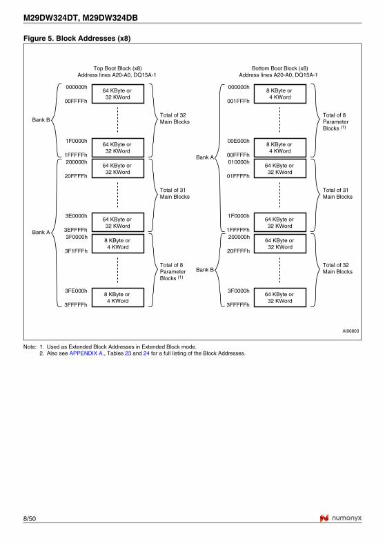
Figure 5. Block Addresses (x8)
Note: 1. Used as Extended Block Addresses in Extended Block mode.2. Also see APPENDIX A., Tables 23 and 24 for a full listing of the Block Addresses.
AI06803
64 KByte or 32 KWord
000000h
00FFFFh
64 KByte or 32 KWord
3E0000h
3EFFFFh
Top Boot Block (x8)Address lines A20-A0, DQ15A-1
64 KByte or 32 KWord
1F0000h
1FFFFFh
Total of 32Main Blocks
64 KByte or 32 KWord
200000h
20FFFFh
8 KByte or 4 KWord
3FE000h
3FFFFFh
8 KByte or 4 KWord
3F0000h
3F1FFFh
Total of 31Main Blocks
Total of 8Parameter Blocks (1)
Bank B
Bank A
8 KByte or 4 KWord
000000h
001FFFh
64 KByte or 32 KWord
1F0000h
1FFFFFh
Bottom Boot Block (x8)Address lines A20-A0, DQ15A-1
8 KByte or 4 KWord
00E000h
00FFFFh
Total of 8Parameter Blocks (1)
64 KByte or 32 KWord
010000h
01FFFFh
64 KByte or 32 KWord
3F0000h
3FFFFFh
64 KByte or 32 KWord
200000h
20FFFFh
Total of 31Main Blocks
Total of 32Main BlocksBank B
Bank A

9/50
M29DW324DT, M29DW324DB
Figure 6. Block Addresses (x16)
Note: 1. Used as Extended Block Addresses in Extended Block mode.2. Also see APPENDIX A., Tables 23 and 24 for a full listing of the Block Addresses.
AI05555
64 KByte or 32 KWord
000000h
007FFFh
64 KByte or 32 KWord
1F0000h
1F7FFFh
Top Boot Block (x16)Address lines A20-A0
64 KByte or 32 KWord
0F8000h
0FFFFFh
Total of 32Main Blocks
64 KByte or 32 KWord
100000h
107FFFh
8 KByte or 4 KWord
1FF000h
1FFFFFh
8 KByte or 4 KWord
1F8000h
1F8FFFh
Total of 31Main Blocks
Total of 8Parameter Blocks (1)
Bank B
Bank A
8 KByte or 4 KWord
000000h
000FFFh
64 KByte or 32 KWord
0F8000h
0FFFFFh
Bottom Boot Block (x16)Address lines A20-A0
8 KByte or 4 KWord
007000h
007FFFh
Total of 8Parameter Blocks (1)
64 KByte or 32 KWord
008000h
00FFFFh
64 KByte or 32 KWord
1F8000h
1FFFFFh
64 KByte or 32 KWord
100000h
107FFFh
Total of 31Main Blocks
Total of 32Main BlocksBank B
Bank A
M29DW324DT, M29DW324DB
10/50
SIGNAL DESCRIPTIONSSee Figure 2., Logic Diagram, and Table 1., SignalNames, for a brief overview of the signals connect-ed to this device.Address Inputs (A0-A20). The Address Inputsselect the cells in the memory array to access dur-ing Bus Read operations. During Bus Write opera-tions they control the commands sent to theCommand Interface of the Program/Erase Con-troller.Data Inputs/Outputs (DQ0-DQ7). The Data I/Ooutputs the data stored at the selected addressduring a Bus Read operation. During Bus Writeoperations they represent the commands sent tothe Command Interface of the Program/EraseController.Data Inputs/Outputs (DQ8-DQ14). The Data I/Ooutputs the data stored at the selected addressduring a Bus Read operation when BYTE is High,VIH. When BYTE is Low, VIL, these pins are notused and are high impedance. During Bus Writeoperations the Command Register does not usethese bits. When reading the Status Registerthese bits should be ignored.Data Input/Output or Address Input (DQ15A–1).When BYTE is High, VIH, this pin behaves as aData Input/Output pin (as DQ8-DQ14). WhenBYTE is Low, VIL, this pin behaves as an addresspin; DQ15A–1 Low will select the LSB of the ad-dressed Word, DQ15A–1 High will select the MSB.Throughout the text consider references to theData Input/Output to include this pin when BYTE isHigh and references to the Address Inputs to in-clude this pin when BYTE is Low except whenstated explicitly otherwise.Chip Enable (E). The Chip Enable, E, activatesthe memory, allowing Bus Read and Bus Write op-erations to be performed. When Chip Enable isHigh, VIH, all other pins are ignored.Output Enable (G). The Output Enable, G, con-trols the Bus Read operation of the memory.Write Enable (W). The Write Enable, W, controlsthe Bus Write operation of the memory’s Com-mand Interface.VPP/Write Protect (VPP/WP). The VPP/WriteProtect pin provides two functions. The VPP func-tion allows the memory to use an external highvoltage power supply to reduce the time requiredfor Program operations. This is achieved by by-passing the unlock cycles and/or using the Dou-ble Word or Quadruple Byte Program commands.The Write Protect function provides a hardwaremethod of protecting the two outermost bootblocks. When VPP/Write Protect is Low, VIL, the memoryprotects the two outermost boot blocks; Program
and Erase operations in these blocks are ignoredwhile VPP/Write Protect is Low, even when RP isat VID.When VPP/Write Protect is High, VIH, the memoryreverts to the previous protection status of the twooutermost boot blocks. Program and Erase oper-ations can now modify the data in these blocks un-less the blocks are protected using BlockProtection.When VPP/Write Protect is raised to VPP the mem-ory automatically enters the Unlock Bypass mode.When VPP/Write Protect returns to VIH or VIL nor-mal operation resumes. During Unlock BypassProgram operations the memory draws IPP fromthe pin to supply the programming circuits. See thedescription of the Unlock Bypass command in theCommand Interface section. The transitions fromVIH to VPP and from VPP to VIH must be slowerthan tVHVPP, see Figure 17.Never raise VPP/Write Protect to VPP from anymode except Read mode, otherwise the memorymay be left in an indeterminate state.The VPP/Write Protect pin must not be left floatingor unconnected or the device may become unreli-able. A 0.1µF capacitor should be connected be-tween the VPP/Write Protect pin and the VSSGround pin to decouple the current surges fromthe power supply. The PCB track widths must besufficient to carry the currents required duringUnlock Bypass Program, IPP.Reset/Block Temporary Unprotect (RP). TheReset/Block Temporary Unprotect pin can beused to apply a Hardware Reset to the memory orto temporarily unprotect all Blocks that have beenprotected.Note that if VPP/WP is at VIL, then the two outer-most boot blocks will remain protected even if RPis at VID.A Hardware Reset is achieved by holding Reset/Block Temporary Unprotect Low, VIL, for at leasttPLPX. After Reset/Block Temporary Unprotectgoes High, VIH, the memory will be ready for BusRead and Bus Write operations after tPHEL ortRHEL, whichever occurs last. See the Ready/BusyOutput section, Table 19. and Figure 16., Reset/Block Temporary Unprotect AC Waveforms, formore details.Holding RP at VID will temporarily unprotect theprotected Blocks in the memory. Program andErase operations on all blocks will be possible.The transition from VIH to VID must be slower thantPHPHH.Ready/Busy Output (RB). The Ready/Busy pinis an open-drain output that can be used to identifywhen the device is performing a Program or Erase
11/50
M29DW324DT, M29DW324DB
operation. During Program or Erase operationsReady/Busy is Low, VOL. Ready/Busy is high-im-pedance during Read mode, Auto Select modeand Erase Suspend mode.After a Hardware Reset, Bus Read and Bus Writeoperations cannot begin until Ready/Busy be-comes high-impedance. See Table 19., Reset/Block Temporary Unprotect AC Characteristicsand Figure 16., Reset/Block Temporary UnprotectAC Waveforms.The use of an open-drain output allows the Ready/Busy pins from several memories to be connectedto a single pull-up resistor. A Low will then indicatethat one, or more, of the memories is busy.Byte/Word Organization Select (BYTE). TheByte/Word Organization Select pin is used toswitch between the x8 and x16 Bus modes of thememory. When Byte/Word Organization Select isLow, VIL, the memory is in x8 mode, when it isHigh, VIH, the memory is in x16 mode.
VCC Supply Voltage (2.7V to 3.6V). VCC pro-vides the power supply for all operations (Read,Program and Erase).The Command Interface is disabled when the VCCSupply Voltage is less than the Lockout Voltage,VLKO. This prevents Bus Write operations from ac-cidentally damaging the data during power up,power down and power surges. If the Program/Erase Controller is programming or erasing duringthis time then the operation aborts and the memo-ry contents being altered will be invalid.A 0.1µF capacitor should be connected betweenthe VCC Supply Voltage pin and the VSS Groundpin to decouple the current surges from the powersupply. The PCB track widths must be sufficient tocarry the currents required during Program andErase operations, ICC3.VSS Ground. VSS is the reference for all voltagemeasurements. The device features two VSS pinswhich must be both connected to the systemground.

M29DW324DT, M29DW324DB
12/50
BUS OPERATIONSThere are five standard bus operations that controlthe device. These are Bus Read, Bus Write, Out-put Disable, Standby and Automatic Standby. The Dual Bank architecture of the M29DW324Dallows read/write operations in Bank A, while readoperations are being executed in Bank B or viceversa. Write operations are only allowed in onebank at a time. See Tables 3 and 4, Bus Operations, for a summa-ry. Typically glitches of less than 5ns on Chip En-able or Write Enable are ignored by the memoryand do not affect bus operations.Bus Read. Bus Read operations read from thememory cells, or specific registers in the Com-mand Interface. A valid Bus Read operation in-volves setting the desired address on the AddressInputs, applying a Low signal, VIL, to Chip Enableand Output Enable and keeping Write EnableHigh, VIH. The Data Inputs/Outputs will output thevalue, see Figure 11., Read Mode AC Waveforms,and Table 15., Read AC Characteristics, for de-tails of when the output becomes valid.Bus Write. Bus Write operations write to theCommand Interface. A valid Bus Write operationbegins by setting the desired address on the Ad-dress Inputs. The Address Inputs are latched bythe Command Interface on the falling edge of ChipEnable or Write Enable, whichever occurs last.The Data Inputs/Outputs are latched by the Com-mand Interface on the rising edge of Chip Enableor Write Enable, whichever occurs first. Output En-able must remain High, VIH, during the whole BusWrite operation. See Figures 12 and 13, Write ACWaveforms, and Tables 16 and 17, Write ACCharacteristics, for details of the timing require-ments.Output Disable. The Data Inputs/Outputs are inthe high impedance state when Output Enable isHigh, VIH.Standby. When Chip Enable is High, VIH, thememory enters Standby mode and the Data In-puts/Outputs pins are placed in the high-imped-
ance state. To reduce the Supply Current to theStandby Supply Current, ICC2, Chip Enable shouldbe held within VCC ± 0.2V. For the Standby currentlevel see Table 14., DC Characteristics.During program or erase operations the memorywill continue to use the Program/Erase SupplyCurrent, ICC3, for Program or Erase operations un-til the operation completes.Automatic Standby. If CMOS levels (VCC ± 0.2V)are used to drive the bus and the bus is inactive for300ns or more the memory enters AutomaticStandby where the internal Supply Current is re-duced to the Standby Supply Current, ICC2. TheData Inputs/Outputs will still output data if a BusRead operation is in progress.Special Bus OperationsAdditional bus operations can be performed toread the Electronic Signature and also to applyand remove Block Protection. These bus opera-tions are intended for use by programming equip-ment and are not usually used in applications.They require VID to be applied to some pins.Electronic Signature. The memory has twocodes, the manufacturer code and the devicecode, that can be read to identify the memory.These codes can be read by applying the signalslisted in Tables 3 and 4, Bus Operations.Block Protect and Chip Unprotect. Groups ofblocks can be protected against accidental Pro-gram or Erase. The Protection Groups are shownin APPENDIX A., Tables 23 and 24, Block Ad-dresses. The whole chip can be unprotected to al-low the data inside the blocks to be changed. The VPP/Write Protect pin can be used to protectthe two outermost boot blocks. When VPP/WriteProtect is at VIL the two outermost boot blocks areprotected and remain protected regardless of theBlock Protection Status or the Reset/Block Tem-porary Unprotect pin status.Block Protect and Chip Unprotect operations aredescribed in APPENDIX D.

13/50
M29DW324DT, M29DW324DB
Table 3. Bus Operations, BYTE = VIL
Note: X = VIL or VIH.
Table 4. Bus Operations, BYTE = VIH
Note: X = VIL or VIH.
Operation E G W Address InputsDQ15A–1, A0-A20
Data Inputs/Outputs
DQ14-DQ8 DQ7-DQ0
Bus Read VIL VIL VIH Cell Address Hi-Z Data Output
Bus Write VIL VIH VIL Command Address Hi-Z Data Input
Output Disable X VIH VIH X Hi-Z Hi-Z
Standby VIH X X X Hi-Z Hi-Z
Read Manufacturer Code
VIL VIL VIHA0 = VIL, A1 = VIL, A9 = VID, Others VIL or VIH
Hi-Z 20h
Read Device Code VIL VIL VIHA0 = VIH, A1 = VIL, A9 = VID, Others VIL or VIH
Hi-Z 5Ch (M29DW324DT)5Dh (M29DW324DB)
Extended Memory Block Verify Code
VIL VIL VIHA0 = VIH, A1 = VIH, A6 = VIL, A9 = VID, Others VIL or VIH
Hi-Z 81h (factory locked)01h (not factory locked)
Operation E G W Address InputsA0-A20
Data Inputs/OutputsDQ15A–1, DQ14-DQ0
Bus Read VIL VIL VIH Cell Address Data Output
Bus Write VIL VIH VIL Command Address Data Input
Output Disable X VIH VIH X Hi-Z
Standby VIH X X X Hi-Z
Read Manufacturer Code
VIL VIL VIHA0 = VIL, A1 = VIL, A9 = VID, Others VIL or VIH
0020h
Read Device Code VIL VIL VIHA0 = VIH, A1 = VIL, A9 = VID, Others VIL or VIH
225Ch (M29DW324DT)225Dh (M29DW324DB)
Extended Memory Block Verify Code
VIL VIL VIHA0 = VIH, A1 = VIH, A6 = VIL, A9 = VID, Others VIL or VIH
81h (factory locked)01h (not factory locked)

M29DW324DT, M29DW324DB
14/50
COMMAND INTERFACEAll Bus Write operations to the memory are inter-preted by the Command Interface. Commandsconsist of one or more sequential Bus Write oper-ations. Failure to observe a valid sequence of BusWrite operations will result in the memory return-ing to Read mode. The long command sequencesare imposed to maximize data security.The address used for the commands changes de-pending on whether the memory is in 16-bit or 8-bit mode. See either Table 5, or 6, depending onthe configuration that is being used, for a summaryof the commands.Read/Reset CommandThe Read/Reset command returns the memory toits Read mode. It also resets the errors in the Sta-tus Register. Either one or three Bus Write opera-tions can be used to issue the Read/Resetcommand.The Read/Reset command can be issued, be-tween Bus Write cycles before the start of a pro-gram or erase operation, to return the device toread mode. If the Read/Reset command is issuedduring the timeout of a Block erase operation thenthe memory will take up to 10µs to abort. Duringthe abort period no valid data can be read from thememory. The Read/Reset command will not abortan Erase operation when issued while in EraseSuspend.Auto Select CommandThe Auto Select command is used to read theManufacturer Code, the Device Code, the BlockProtection Status and the Extended Memory BlockVerify Code. It can be addressed to either Bank.Three consecutive Bus Write operations are re-quired to issue the Auto Select command. The fi-nal Write cycle must be addressed to one of theBanks. Once the Auto Select command is issuedBus Read operations to the Bank where the com-mand was issued output the Auto Select data. BusRead operations to the other Bank will output thecontents of the memory array. The memory re-mains in Auto Select mode until a Read/Reset orCFI Query command is issued. In Auto Select mode the Manufacturer Code canbe read using a Bus Read operation with A0 = VILand A1 = VIL and A20 = Bank Address. The otheraddress bits may be set to either VIL or VIH. The Device Code can be read using a Bus Readoperation with A0 = VIH and A1 = VIL and A20 =Bank Address. The other address bits may be setto either VIL or VIH. The Block Protection Status of each block can beread using a Bus Read operation with A0 = VIL,A1 = VIH, A20 = Bank Address and A12-A19 spec-ifying the address of the block inside the Bank.
The other address bits may be set to either VIL orVIH. If the addressed block is protected then 01h isoutput on Data Inputs/Outputs DQ0-DQ7, other-wise 00h is output.Read CFI Query CommandThe Read CFI Query Command is used to readdata from the Common Flash Interface (CFI)Memory Area. This command is valid when the de-vice is in the Read Array mode, or when the deviceis in Auto Select mode. One Bus Write cycle is required to issue the ReadCFI Query Command. Once the command is is-sued subsequent Bus Read operations read fromthe Common Flash Interface Memory Area.The Read/Reset command must be issued to re-turn the device to the previous mode (the Read Ar-ray mode or Auto Select mode). A second Read/Reset command would be needed if the device isto be put in the Read Array mode from Auto Selectmode.See APPENDIX B., Tables 25, 26, 27, 28, 29 and30 for details on the information contained in theCommon Flash Interface (CFI) memory area.Program CommandThe Program command can be used to program avalue to one address in the memory array at atime. The command requires four Bus Write oper-ations, the final write operation latches the ad-dress and data, and starts the Program/EraseController. If the address falls in a protected block then theProgram command is ignored, the data remainsunchanged. The Status Register is never read andno error condition is given.During the program operation the memory will ig-nore all commands. It is not possible to issue anycommand to abort or pause the operation. Afterprogramming has started, Bus Read operations inthe Bank being programmed output the StatusRegister content, while Bus Read operations tothe other Bank output the contents of the memoryarray. See the section on the Status Register formore details. Typical program times are given inTable 7.After the program operation has completed thememory will return to the Read mode, unless anerror has occurred. When an error occurs BusRead operations to the Bank where the commandwas issued will continue to output the Status Reg-ister. A Read/Reset command must be issued toreset the error condition and return to Read mode.Note that the Program command cannot change abit set at ’0’ back to ’1’. One of the Erase Com-mands must be used to set all the bits in a block orin the whole memory from ’0’ to ’1’.

15/50
M29DW324DT, M29DW324DB
Fast Program CommandsThere are two Fast Program commands availableto improve the programming throughput, by writingseveral adjacent words or bytes in parallel. TheQuadruple Byte Program command is available forx8 operations, while the Double Word Programcommand is available for x16 operations.Only one bank can be programmed at any onetime. The other bank must be in Read mode orErase Suspend.Fast Program commands should not be attemptedwhen VPP is not at VPP. Care must be taken be-cause applying a 12V VPP voltage to the VPP/WPpin will temporarily unprotect any protected block.After programming has started, Bus Read opera-tions in the Bank being programmed output theStatus Register content, while Bus Read opera-tions to the other Bank output the contents of thememory array.After the program operation has completed thememory will return to the Read mode, unless anerror has occurred. When an error occurs BusRead operations to the Bank where the commandwas issued will continue to output the Status Reg-ister. A Read/Reset command must be issued toreset the error condition and return to Read mode.Note that the Fast Program commands cannotchange a bit set at ’0’ back to ’1’. One of the EraseCommands must be used to set all the bits in ablock or in the whole memory from ’0’ to ’1’.Typical Program times are given in Table 7., Pro-gram, Erase Times and Program, Erase Endur-ance Cycles.
Quadruple Byte Program Command. The Qua-druple Byte Program command is used to write apage of four adjacent Bytes in parallel. The fourbytes must differ only for addresses A0, DQ15A-1.Five bus write cycles are necessary to issue theQuadruple Byte Program command.■ The first bus cycle sets up the Quadruple Byte
Program Command.■ The second bus cycle latches the Address and
the Data of the first byte to be written.■ The third bus cycle latches the Address and
the Data of the second byte to be written.■ The fourth bus cycle latches the Address and
the Data of the third byte to be written.■ The fifth bus cycle latches the Address and the
Data of the fourth byte to be written and starts the Program/Erase Controller.
Double Word Program Command. The DoubleWord Program command is used to write a pageof two adjacent words in parallel. The two wordsmust differ only for the address A0.
Three bus write cycles are necessary to issue theDouble Word Program command.■ The first bus cycle sets up the Double Word
Program Command.■ The second bus cycle latches the Address and
the Data of the first word to be written.■ The third bus cycle latches the Address and
the Data of the second word to be written and starts the Program/Erase Controller.
Unlock Bypass Command.The Unlock Bypass command is used in conjunc-tion with the Unlock Bypass Program command toprogram the memory faster than with the standardprogram commands. When the cycle time to thedevice is long, considerable time saving can bemade by using these commands. Three Bus Writeoperations are required to issue the Unlock By-pass command.Once the Unlock Bypass command has been is-sued the bank enters Unlock Bypass mode. Whenin Unlock Bypass mode, only the Unlock BypassProgram and Unlock Bypass Reset commandsare valid. The Unlock Bypass Program commandcan be issued to program addresses within thebank, and the Unlock Bypass Reset command toreturn the bank to Read mode. In Unlock Bypassmode the memory can be read as if in Read mode. When VPP is applied to the VPP/Write Protect pinthe memory automatically enters the Unlock By-pass mode and the Unlock Bypass Program com-mand can be issued immediately. Care must betaken because applying a 12V VPP voltage to theVPP/WP pin will temporarily unprotect any protect-ed block.Unlock Bypass Program Command.The Unlock Bypass Program command can beused to program one address in the memory arrayat a time. The command requires two Bus Writeoperations, the final write operation latches the ad-dress and data, and starts the Program/EraseController.The Program operation using the Unlock BypassProgram command behaves identically to the Pro-gram operation using the Program command. Theoperation cannot be aborted, a Bus Read opera-tion to the Bank where the command was issuedoutputs the Status Register. See the Programcommand for details on the behavior.Unlock Bypass Reset Command.The Unlock Bypass Reset command can be usedto return to Read/Reset mode from Unlock BypassMode. Two Bus Write operations are required toissue the Unlock Bypass Reset command. Read/Reset command does not exit from Unlock BypassMode.
M29DW324DT, M29DW324DB
16/50
Chip Erase Command.The Chip Erase command can be used to erasethe entire chip. Six Bus Write operations are re-quired to issue the Chip Erase Command and startthe Program/Erase Controller.If any blocks are protected then these are ignoredand all the other blocks are erased. If all of theblocks are protected the Chip Erase operation ap-pears to start but will terminate within about 100µs,leaving the data unchanged. No error condition isgiven when protected blocks are ignored.During the erase operation the memory will ignoreall commands, including the Erase Suspend com-mand. It is not possible to issue any command toabort the operation. Typical chip erase times aregiven in Table 7. All Bus Read operations duringthe Chip Erase operation will output the StatusRegister on the Data Inputs/Outputs. See the sec-tion on the Status Register for more details.After the Chip Erase operation has completed thememory will return to the Read Mode, unless anerror has occurred. When an error occurs thememory will continue to output the Status Regis-ter. A Read/Reset command must be issued to re-set the error condition and return to Read Mode.The Chip Erase Command sets all of the bits in un-protected blocks of the memory to ’1’. All previousdata is lost.Block Erase Command.The Block Erase command can be used to erasea list of one or more blocks in a Bank. It sets all ofthe bits in the unprotected selected blocks to ’1’.All previous data in the selected blocks is lost.Six Bus Write operations are required to select thefirst block in the list. Each additional block in thelist can be selected by repeating the sixth BusWrite operation using the address of the additionalblock. All blocks must belong to the same Bank; ifa block belonging to the other Bank is given it willnot be erased. The Block Erase operation startsthe Program/Erase Controller after a time-out pe-riod of 50µs after the last Bus Write operation.Once the Program/Erase Controller starts it is notpossible to select any more blocks. Each addition-al block must therefore be selected within 50µs ofthe last block. The 50µs timer restarts when an ad-ditional block is selected. After the sixth Bus Writeoperation a Bus Read operation within the sameBank will output the Status Register. See the Sta-tus Register section for details on how to identify ifthe Program/Erase Controller has started theBlock Erase operation.If any selected blocks are protected then these areignored and all the other selected blocks areerased. If all of the selected blocks are protectedthe Block Erase operation appears to start but will
terminate within about 100µs, leaving the data un-changed. No error condition is given when protect-ed blocks are ignored.During the Block Erase operation the memory willignore all commands except the Erase Suspendcommand and the Read/Reset command which isonly accepted during the 50µs time-out period.Typical block erase times are given in Table 7. After the Erase operation has started all Bus Readoperations to the Bank being erased will output theStatus Register on the Data Inputs/Outputs. Seethe section on the Status Register for more details.After the Block Erase operation has completed thememory will return to the Read Mode, unless anerror has occurred. When an error occurs BusRead operations to the Bank where the commandwas issued will continue to output the Status Reg-ister. A Read/Reset command must be issued toreset the error condition and return to Read mode.Erase Suspend Command.The Erase Suspend Command may be used totemporarily suspend a Block Erase operation andreturn the memory to Read mode. The commandrequires one Bus Write operation.The Program/Erase Controller will suspend withinthe Erase Suspend Latency time of the Erase Sus-pend Command being issued. Once the Program/Erase Controller has stopped the memory will beset to Read mode and the Erase will be suspend-ed. If the Erase Suspend command is issued dur-ing the period when the memory is waiting for anadditional block (before the Program/Erase Con-troller starts) then the Erase is suspended immedi-ately and will start immediately when the EraseResume Command is issued. It is not possible toselect any further blocks to erase after the EraseResume.During Erase Suspend it is possible to Read andProgram cells in blocks that are not being erased;both Read and Program operations behave asnormal on these blocks. If any attempt is made toprogram in a protected block or in the suspendedblock then the Program command is ignored andthe data remains unchanged. The Status Registeris not read and no error condition is given. Read-ing from blocks that are being erased will outputthe Status Register. It is also possible to issue the Auto Select, ReadCFI Query and Unlock Bypass commands duringan Erase Suspend. The Read/Reset commandmust be issued to return the device to Read Arraymode before the Resume command will be ac-cepted.During Erase Suspend a Bus Read operation tothe Extended Block will output the Extended Blockdata.

17/50
M29DW324DT, M29DW324DB
Erase Resume Command.The Erase Resume command must be used to re-start the Program/Erase Controller after an EraseSuspend. The device must be in Read Array modebefore the Resume command will be accepted. Anerase can be suspended and resumed more thanonce.Enter Extended Block CommandThe M29DW324D has an extra 64KByte block(Extended Block) that can only be accessed usingthe Enter Extended Block command. Three Buswrite cycles are required to issue the ExtendedBlock command. Once the command has been is-sued the device enters Extended Block modewhere all Bus Read or Program operations to theBoot Block addresses access the Extended Block.The Extended Block (with the same address asthe boot block) cannot be erased, and can betreated as one-time programmable (OTP) memo-ry. In Extended Block mode the Boot Blocks arenot accessible. In Extended Block mode dual op-erations are possible, with the Extended Block
mapped in Bank A. When in Extended Blockmode, Erase Commands in Bank A are not al-lowed. To exit from the Extended Block mode the Exit Ex-tended Block command must be issued. The Extended Block can be protected, howeveronce protected the protection cannot be undone. Exit Extended Block Command.The Exit Extended Block command is used to exitfrom the Extended Block mode and return the de-vice to Read mode. Four Bus Write operations arerequired to issue the command. Block Protect and Chip Unprotect Commands.Groups of blocks can be protected against acci-dental Program or Erase. The Protection Groupsare shown in APPENDIX A., Tables 23 and 24,Block Addresses. The whole chip can be unpro-tected to allow the data inside the blocks to bechanged. Block Protect and Chip Unprotect oper-ations are described in APPENDIX D.
Table 5. Commands, 16-bit mode, BYTE = VIH
Note: X Don’t Care, PA Program Address, PD Program Data, BA Any address in the Block, BKA Bank Address. All values in the table are inhexadecimal.The Command Interface only uses A–1, A0-A10 and DQ0-DQ7 to verify the commands; A11-A20, DQ8-DQ14 and DQ15 are Don’tCare. DQ15A–1 is A–1 when BYTE is VIL or DQ15 when BYTE is VIH.
Command
Len
gth
Bus Write Operations
1st 2nd 3rd 4th 5th 6th
Addr Data Addr Data Addr Data Addr Data Addr Data Addr Data
Read/Reset1 X F0
3 555 AA 2AA 55 X F0
Auto Select 3 555 AA 2AA 55 (BKA)555 90
Program 4 555 AA 2AA 55 555 A0 PA PD
Double Word Program 3 555 50 PA0 PD0 PA1 PD1
Unlock Bypass 3 555 AA 2AA 55 555 20
Unlock Bypass Program 2 X A0 PA PD
Unlock Bypass Reset 2 X 90 X 00
Chip Erase 6 555 AA 2AA 55 555 80 555 AA 2AA 55 555 10
Block Erase 6+ 555 AA 2AA 55 555 80 555 AA 2AA 55 BA 30
Erase Suspend 1 BKA B0
Erase Resume 1 BKA 30
Read CFI Query 1 55 98
Enter Extended Block 3 555 AA 2AA 55 555 88
Exit Extended Block 4 555 AA 2AA 55 555 90 X 00

M29DW324DT, M29DW324DB
18/50
Table 6. Commands, 8-bit mode, BYTE = VIL
Note: X Don’t Care, PA Program Address, PD Program Data, BA Any address in the Block. All values in the table are in hexadecimal.The Command Interface only uses A–1, A0-A10 and DQ0-DQ7 to verify the commands; A11-A20, DQ8-DQ14 and DQ15 are Don’tCare. DQ15A–1 is A–1 when BYTE is VIL or DQ15 when BYTE is VIH.
Table 7. Program, Erase Times and Program, Erase Endurance Cycles
Note: 1. Typical values measured at room temperature and nominal voltages.2. Sampled, but not 100% tested.3. Maximum value measured at worst case conditions for both temperature and VCC after 100,00 program/erase cycles.4. Maximum value measured at worst case conditions for both temperature and VCC.
Command
Len
gth
Bus Write Operations
1st 2nd 3rd 4th 5th 6th
Add Data Add Data Add Data Add Data Add Data Add Data
Read/Reset1 X F0
3 AAA AA 555 55 X F0
Auto Select 3 AAA AA 555 55 (BKA)AAA 90
Program 4 AAA AA 555 55 AAA A0 PA PD
Quadruple Byte Program 5 AAA 55 PA0 PD0 PA1 PD1 PA2 PD2 PA3 PD3
Unlock Bypass 3 AAA AA 555 55 AAA 20
Unlock Bypass Program 2 X A0 PA PD
Unlock Bypass Reset 2 X 90 X 00
Chip Erase 6 AAA AA 555 55 AAA 80 AAA AA 555 55 AAA 10
Block Erase 6+ AAA AA 555 55 AAA 80 AAA AA 555 55 BA 30
Erase Suspend 1 BKA B0
Erase Resume 1 BKA 30
Read CFI Query 1 AA 98
Enter Extended Block 3 AAA AA 555 55 AAA 88
Exit Extended Block 4 AAA AA 555 55 AAA 90 X 00
Parameter Min Typ (1, 2) Max(2) Unit
Chip Erase 40 200(3) s
Block Erase (64 KBytes) 0.8 6(3) s
Erase Suspend Latency time 50(4) µs
Program (Byte or Word) 10 200(4) µs
Double Word Program (Byte or Word) 10 200(3) µs
Chip Program (Byte by Byte) 40 200(3) s
Chip Program (Word by Word) 20 100(3) s
Chip Program (Quadruple Byte or Double Word) 10 100 s
Program/Erase Cycles (per Block) 100,000 cycles
Data Retention 20 years

19/50
M29DW324DT, M29DW324DB
STATUS REGISTERThe M29DW324D has a Status Register that pro-vides information on the current or previous Pro-gram or Erase operations executed in each bank.The various bits convey information and errors onthe operation. Bus Read operations from any ad-dress within the Bank, always read the StatusRegister during Program and Erase operations. Itis also read during Erase Suspend when an ad-dress within a block being erased is accessed.The bits in the Status Register are summarized inTable 8., Status Register Bits.Data Polling Bit (DQ7). The Data Polling Bit canbe used to identify whether the Program/EraseController has successfully completed its opera-tion or if it has responded to an Erase Suspend.The Data Polling Bit is output on DQ7 when theStatus Register is read.During Program operations the Data Polling Bitoutputs the complement of the bit being pro-grammed to DQ7. After successful completion ofthe Program operation the memory returns toRead mode and Bus Read operations from the ad-dress just programmed output DQ7, not its com-plement.During Erase operations the Data Polling Bit out-puts ’0’, the complement of the erased state ofDQ7. After successful completion of the Erase op-eration the memory returns to Read Mode.In Erase Suspend mode the Data Polling Bit willoutput a ’1’ during a Bus Read operation within ablock being erased. The Data Polling Bit willchange from a ’0’ to a ’1’ when the Program/EraseController has suspended the Erase operation.Figure 7., Data Polling Flowchart, gives an exam-ple of how to use the Data Polling Bit. A Valid Ad-dress is the address being programmed or anaddress within the block being erased.Toggle Bit (DQ6). The Toggle Bit can be used toidentify whether the Program/Erase Controller hassuccessfully completed its operation or if it has re-sponded to an Erase Suspend. The Toggle Bit isoutput on DQ6 when the Status Register is read.During Program and Erase operations the ToggleBit changes from ’0’ to ’1’ to ’0’, etc., with succes-sive Bus Read operations at any address. Aftersuccessful completion of the operation the memo-ry returns to Read mode.During Erase Suspend mode the Toggle Bit willoutput when addressing a cell within a block beingerased. The Toggle Bit will stop toggling when theProgram/Erase Controller has suspended theErase operation.Figure 8., Toggle Flowchart, gives an example ofhow to use the Data Toggle Bit. Figures 14 and 15describe Toggle Bit timing waveform.
Error Bit (DQ5). The Error Bit can be used toidentify errors detected by the Program/EraseController. The Error Bit is set to ’1’ when a Pro-gram, Block Erase or Chip Erase operation fails towrite the correct data to the memory. If the ErrorBit is set a Read/Reset command must be issuedbefore other commands are issued. The Error bitis output on DQ5 when the Status Register is read.Note that the Program command cannot change abit set to ’0’ back to ’1’ and attempting to do so willset DQ5 to ‘1’. A Bus Read operation to that ad-dress will show the bit is still ‘0’. One of the Erasecommands must be used to set all the bits in ablock or in the whole memory from ’0’ to ’1’.Erase Timer Bit (DQ3). The Erase Timer Bit canbe used to identify the start of Program/EraseController operation during a Block Erase com-mand. Once the Program/Erase Controller startserasing the Erase Timer Bit is set to ’1’. Before theProgram/Erase Controller starts the Erase TimerBit is set to ’0’ and additional blocks to be erasedmay be written to the Command Interface. TheErase Timer Bit is output on DQ3 when the StatusRegister is read.Alternative Toggle Bit (DQ2). The AlternativeToggle Bit can be used to monitor the Program/Erase controller during Erase operations. The Al-ternative Toggle Bit is output on DQ2 when theStatus Register is read.During Chip Erase and Block Erase operations theToggle Bit changes from ’0’ to ’1’ to ’0’, etc., withsuccessive Bus Read operations from addresseswithin the blocks being erased. A protected blockis treated the same as a block not being erased.Once the operation completes the memory returnsto Read mode.During Erase Suspend the Alternative Toggle Bitchanges from ’0’ to ’1’ to ’0’, etc. with successiveBus Read operations from addresses within theblocks being erased. Bus Read operations to ad-dresses within blocks not being erased will outputthe memory cell data as if in Read mode.After an Erase operation that causes the Error Bitto be set the Alternative Toggle Bit can be used toidentify which block or blocks have caused the er-ror. The Alternative Toggle Bit changes from ’0’ to’1’ to ’0’, etc. with successive Bus Read Opera-tions from addresses within blocks that have noterased correctly. The Alternative Toggle Bit doesnot change if the addressed block has erased cor-rectly.Figures 14 and 15 describe Alternative Toggle Bittiming waveform.

M29DW324DT, M29DW324DB
20/50
Table 8. Status Register Bits
Note: Unspecified data bits should be ignored.
Figure 7. Data Polling Flowchart Figure 8. Toggle Flowchart
Note: BA = Address of Bank being Programmed or Erased.
Operation Address DQ7 DQ6 DQ5 DQ3 DQ2 RB
Program Bank Address DQ7 Toggle 0 – – 0
Program During Erase Suspend Bank Address DQ7 Toggle 0 – – 0
Program Error Bank Address DQ7 Toggle 1 – – Hi-Z
Chip Erase Any Address 0 Toggle 0 1 Toggle 0
Block Erase before timeout
Erasing Block 0 Toggle 0 0 Toggle 0
Non-Erasing Block 0 Toggle 0 0 No Toggle 0
Block EraseErasing Block 0 Toggle 0 1 Toggle 0
Non-Erasing Block 0 Toggle 0 1 No Toggle 0
Erase SuspendErasing Block 1 No Toggle 0 – Toggle Hi-Z
Non-Erasing Block Data read as normal Hi-Z
Erase ErrorGood Block Address 0 Toggle 1 1 No Toggle Hi-Z
Faulty Block Address 0 Toggle 1 1 Toggle Hi-Z
READ DQ5 & DQ7at VALID ADDRESS
START
READ DQ7at VALID ADDRESS
FAIL PASS
AI90194
DQ7=
DATA
YES
NO
YES
NO
DQ5= 1
DQ7=
DATA
YES
NO
READ DQ6ADDRESS = BA
START
READ DQ6TWICE
ADDRESS = BA
FAIL PASS
AI08929b
DQ6=
TOGGLENO
NO
YES
YES
DQ5= 1
NO
YES
DQ6=
TOGGLE
READDQ5 & DQ6
ADDRESS = BA

21/50
M29DW324DT, M29DW324DB
DUAL OPERATIONS AND MULTIPLE BANK ARCHITECTUREThe Multiple Bank Architecture of theM29DW324DT and M29DW324DB gives greaterflexibility for software developers to split the codeand data spaces within the memory array. TheDual Operations feature simplifies the softwaremanagement of the device by allowing code to beexecuted from one bank while the other bank isbeing programmed or erased.The Dual Operations feature means that while pro-gramming or erasing in one bank, read operationsare possible in the other bank with zero latency. Only one bank at a time is allowed to be in pro-gram or erase mode.
If a read operation is required in a bank, which isprogramming or erasing, the program or erase op-eration can be suspended. Also if the suspended operation was erase then aprogram command can be issued to anotherblock, so the device can have one block in EraseSuspend mode, one programming and otherbanks in read mode. By using a combination of these features, read op-erations are possible at any moment. Table 9. and Table 10. show the dual operationspossible in other banks and in the same bank.Note that only the commonly used commands arerepresented in these tables.
Table 9. Dual Operations Allowed In the Other Bank
Note: 1. If one bank is involved in a program or erase operation, then the other bank is available for dual operations.2. Only after an Erase operation in that bank.3. Only after an Erase Suspend command in that bank.
Table 10. Dual Operations Allowed In Same Bank
Note: 1. Not allowed in the Block or Word that is being erased or programmed.2. Only after an Erase operation in that bank.3. Only after an Erase Suspend command in that bank.4. Read Status Register is not a command. The Status Register can be read during a block program or erase operation.5. The Status Register can be read by addressing the block being erase suspended.
Status of First Bank(1)
Commands allowed in the Other Bank(1)
Read Array
Read Status Register(6)
Read CFI
Query
AutoSelect Program Erase Erase
SuspendErase
Resume
Idle Yes Yes(2) Yes Yes Yes Yes Yes(2) Yes(3)
Programming Yes No No No – – No No
Erasing Yes No No No – – No No
Erase Suspended Yes Yes Yes Yes Yes No - Yes
Status of bank
Commands allowed in same bank
Read Array
Read Status
Register(4)
Read CFI Query
AutoSelect Program Erase Erase
SuspendErase
Resume
Idle Yes Yes Yes Yes Yes Yes Yes(2) Yes(3)
Programming No Yes No No – – No -
Erasing No Yes No No – No Yes(5) -
Erase Suspended Yes(1) Yes(5) Yes Yes Yes(1) No - Yes(4)
M29DW324DT, M29DW324DB
22/50
MAXIMUM RATINGStressing the device above the rating listed in theAbsolute Maximum Ratings table may cause per-manent damage to the device. Exposure to Abso-lute Maximum Rating conditions for extendedperiods may affect device reliability. These are
stress ratings only and operation of the device atthese or any other conditions above those indicat-ed in the Operating sections of this specification isnot implied. Refer also to the Numonyx SURE Pro-gram and other relevant quality documents.
Table 11. Absolute Maximum Ratings
Note: 1. Compliant with the JEDEC Std J-STD-020B (for small body, Sn-Pb or Pb assembly), and the European directive on Restrictions onHazardous Substances (RoHS) 2002/95/EU.
2. Minimum voltage may undershoot to –2V during transition and for less than 20ns during transitions.3. Maximum voltage may overshoot to VCC +2V during transition and for less than 20ns during transitions.4. VPP must not remain at 12V for more than a total of 80hrs.
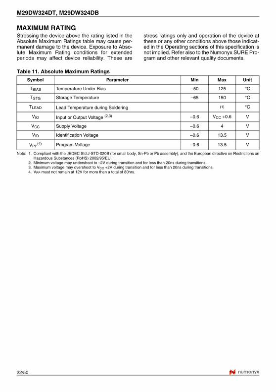
Symbol Parameter Min Max Unit
TBIAS Temperature Under Bias –50 125 °C
TSTG Storage Temperature –65 150 °C
TLEAD Lead Temperature during Soldering (1) °C
VIO Input or Output Voltage (2,3) –0.6 VCC +0.6 V
VCC Supply Voltage –0.6 4 V
VID Identification Voltage –0.6 13.5 V
VPP(4) Program Voltage –0.6 13.5 V
23/50
M29DW324DT, M29DW324DB
DC AND AC PARAMETERSThis section summarizes the operating measure-ment conditions, and the DC and AC characteris-tics of the device. The parameters in the DC andAC characteristics Tables that follow, are derivedfrom tests performed under the Measurement
Conditions summarized in Table 12., Operatingand AC Measurement Conditions. Designersshould check that the operating conditions in theircircuit match the operating conditions when rely-ing on the quoted parameters.
Table 12. Operating and AC Measurement Conditions
Figure 9. AC Measurement I/O Waveform Figure 10. AC Measurement Load Circuit
Table 13. Device Capacitance
Note: Sampled only, not 100% tested.
Parameter
M29DW324D
Unit70 90
Min Max Min Max
VCC Supply Voltage 2.7 3.6 2.7 3.6 V
Ambient Operating Temperature –40 85 –40 85 °C
Load Capacitance (CL) 30 30 pF
Input Rise and Fall Times 10 10 ns
Input Pulse Voltages 0 to VCC 0 to VCC V
Input and Output Timing Ref. Voltages VCC/2 VCC/2 V
AI05557
VCC
0V
VCC/2
AI05558
CL
CL includes JIG capacitance
DEVICEUNDERTEST
25kΩ
VCC
25kΩ
VCC
0.1µF
VPP
0.1µF
Symbol Parameter Test Condition Min Max Unit
CIN Input Capacitance VIN = 0V 6 pF
COUT Output Capacitance VOUT = 0V 12 pF
M29DW324DT, M29DW324DB
24/50
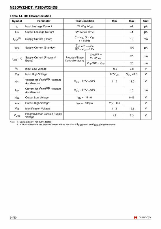
Table 14. DC Characteristics
Note: 1. Sampled only, not 100% tested.2. In Dual operations the Supply Current will be the sum of ICC1(read) and ICC3 (program/erase).
Symbol Parameter Test Condition Min Max Unit
ILI Input Leakage Current 0V ≤ VIN ≤ VCC ±1 µA
ILO Output Leakage Current 0V ≤ VOUT ≤ VCC ±1 µA
ICC1(2) Supply Current (Read)
E = VIL, G = VIH,f = 6MHz
10 mA
ICC2 Supply Current (Standby)E = VCC ±0.2V,
RP = VCC ±0.2V 100 µA
ICC3 (1,2) Supply Current (Program/Erase)
Program/EraseController active
VPP/WP = VIL or VIH
20 mA
VPP/WP = VPP 20 mA
VIL Input Low Voltage –0.5 0.8 V
VIH Input High Voltage 0.7VCC VCC +0.3 V
VPPVoltage for VPP/WP Program Acceleration
VCC = 2.7V ±10% 11.5 12.5 V
IPPCurrent for VPP/WP Program Acceleration
VCC = 2.7V ±10% 15 mA
VOL Output Low Voltage IOL = 1.8mA 0.45 V
VOH Output High Voltage IOH = –100µA VCC –0.4 V
VID Identification Voltage 11.5 12.5 V
VLKOProgram/Erase Lockout Supply Voltage 1.8 2.3 V

25/50
M29DW324DT, M29DW324DB
Figure 11. Read Mode AC Waveforms
Table 15. Read AC Characteristics
Note: 1. Sampled only, not 100% tested.
Symbol Alt Parameter Test ConditionM29DW324D
Unit70 90
tAVAV tRC Address Valid to Next Address ValidE = VIL,G = VIL
Min 70 90 ns
tAVQV tACC Address Valid to Output ValidE = VIL,G = VIL
Max 70 90 ns
tELQX (1) tLZ Chip Enable Low to Output Transition G = VIL Min 0 0 ns
tELQV tCE Chip Enable Low to Output Valid G = VIL Max 70 90 ns
tGLQX (1) tOLZ Output Enable Low to Output Transition E = VIL Min 0 0 ns
tGLQV tOE Output Enable Low to Output Valid E = VIL Max 30 35 ns
tEHQZ (1) tHZ Chip Enable High to Output Hi-Z G = VIL Max 25 30 ns
tGHQZ (1) tDF Output Enable High to Output Hi-Z E = VIL Max 25 30 ns
tEHQXtGHQXtAXQX
tOHChip Enable, Output Enable or Address Transition to Output Transition Min 0 0 ns
tELBLtELBH
tELFLtELFH
Chip Enable to BYTE Low or High Max 5 5 ns
tBLQZ tFLQZ BYTE Low to Output Hi-Z Max 25 30 ns
tBHQV tFHQV BYTE High to Output Valid Max 30 40 ns
AI05559
tAVAV
tAVQV tAXQX
tELQX tEHQZ
tGLQV
tGLQX tGHQX
VALID
A0-A21/A–1
G
DQ0-DQ7/DQ8-DQ15
E
tELQV tEHQX
tGHQZ
VALID
tBHQV
tELBL/tELBH tBLQZ
BYTE
M29DW324DT, M29DW324DB
26/50
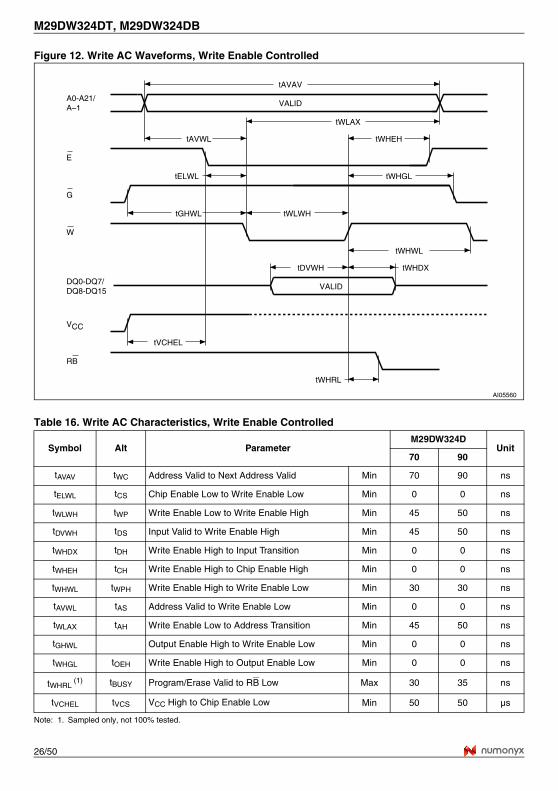
Figure 12. Write AC Waveforms, Write Enable Controlled
Table 16. Write AC Characteristics, Write Enable Controlled
Note: 1. Sampled only, not 100% tested.
Symbol Alt ParameterM29DW324D
Unit70 90
tAVAV tWC Address Valid to Next Address Valid Min 70 90 ns
tELWL tCS Chip Enable Low to Write Enable Low Min 0 0 ns
tWLWH tWP Write Enable Low to Write Enable High Min 45 50 ns
tDVWH tDS Input Valid to Write Enable High Min 45 50 ns
tWHDX tDH Write Enable High to Input Transition Min 0 0 ns
tWHEH tCH Write Enable High to Chip Enable High Min 0 0 ns
tWHWL tWPH Write Enable High to Write Enable Low Min 30 30 ns
tAVWL tAS Address Valid to Write Enable Low Min 0 0 ns
tWLAX tAH Write Enable Low to Address Transition Min 45 50 ns
tGHWL Output Enable High to Write Enable Low Min 0 0 ns
tWHGL tOEH Write Enable High to Output Enable Low Min 0 0 ns
tWHRL (1) tBUSY Program/Erase Valid to RB Low Max 30 35 ns
tVCHEL tVCS VCC High to Chip Enable Low Min 50 50 µs
AI05560
E
G
W
A0-A21/A–1
DQ0-DQ7/DQ8-DQ15
VALID
VALID
VCC
tVCHEL
tWHEH
tWHWL
tELWL
tAVWL
tWHGL
tWLAX
tWHDX
tAVAV
tDVWH
tWLWHtGHWL
RB
tWHRL
27/50
M29DW324DT, M29DW324DB
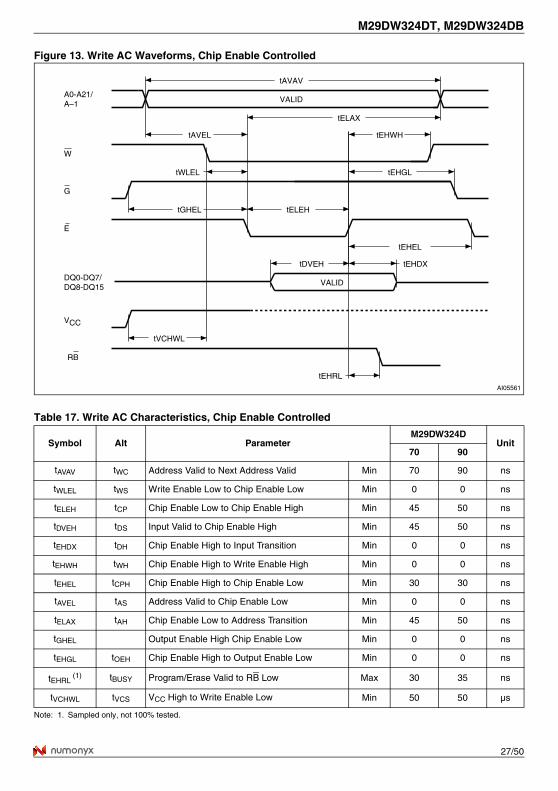
Figure 13. Write AC Waveforms, Chip Enable Controlled
Table 17. Write AC Characteristics, Chip Enable Controlled
Note: 1. Sampled only, not 100% tested.
Symbol Alt ParameterM29DW324D
Unit70 90
tAVAV tWC Address Valid to Next Address Valid Min 70 90 ns
tWLEL tWS Write Enable Low to Chip Enable Low Min 0 0 ns
tELEH tCP Chip Enable Low to Chip Enable High Min 45 50 ns
tDVEH tDS Input Valid to Chip Enable High Min 45 50 ns
tEHDX tDH Chip Enable High to Input Transition Min 0 0 ns
tEHWH tWH Chip Enable High to Write Enable High Min 0 0 ns
tEHEL tCPH Chip Enable High to Chip Enable Low Min 30 30 ns
tAVEL tAS Address Valid to Chip Enable Low Min 0 0 ns
tELAX tAH Chip Enable Low to Address Transition Min 45 50 ns
tGHEL Output Enable High Chip Enable Low Min 0 0 ns
tEHGL tOEH Chip Enable High to Output Enable Low Min 0 0 ns
tEHRL (1) tBUSY Program/Erase Valid to RB Low Max 30 35 ns
tVCHWL tVCS VCC High to Write Enable Low Min 50 50 µs
AI05561
E
G
W
A0-A21/A–1
DQ0-DQ7/DQ8-DQ15
VALID
VALID
VCC
tVCHWL
tEHWH
tEHEL
tWLEL
tAVEL
tEHGL
tELAX
tEHDX
tAVAV
tDVEH
tELEHtGHEL
RB
tEHRL

M29DW324DT, M29DW324DB
28/50
Figure 14. Toggle and Alternative Toggle Bits Mechanism, Chip Enable Controlled
Note: 1. The Toggle bit is output on DQ6. 2. The Alternative Toggle bit is output on DQ2.
Figure 15. Toggle and Alternative Toggle Bits Mechanism, Output Enable Controlled
Note: 1. The Toggle bit is output on DQ6. 2. The Alternative Toggle bit is output on DQ2.
Table 18. Toggle and Alternative Toggle Bits AC Characteristics
Note: tELQV and tGLQV values are presented in Table 15., Read AC Characteristics.
Symbol Alt ParameterM29DW323D
Unit70 90
tAXEL Address Transition to Chip Enable Low Min 10 10 ns
tAXGL Address Transition to Output Enable Low Min 10 10 ns
AI08914c
G
A0-A20
DQ2(1)/DQ6(2)
E
tAXEL
tELQV
Data DataToggle/Alternative Toggle Bit
tELQV
Address in the Bank Being Programmed or Erased
Read Operation outside the Bank Being Programmed or Erased
Address Outside the Bank Being Programmed or Erased
Address Outside the Bank Being Programmed or Erased
Toggle/Alternative Toggle Bit
Read Operation Outside the Bank Being Programmed or Erased
Read Operation in the Bank Being Programmed or Erased
AI08915c
G
A0-A20
DQ2(1)/DQ6(2)
E
tAXGL
tGLQV
Data DataToggle/Alternative Toggle Bit
tGLQV
Address in the Bank Being Programmed or Erased
Read Operation outside the Bank Being Programmed or Erased
Address Outside the Bank Being Programmed or Erased
Address Outside the Bank Being Programmed or Erased
Toggle/Alternative Toggle Bit
Read Operation Outside the Bank Being Programmed or Erased
Read Operation in the Bank Being Programmed or Erased

29/50
M29DW324DT, M29DW324DB
Figure 16. Reset/Block Temporary Unprotect AC Waveforms
Table 19. Reset/Block Temporary Unprotect AC Characteristics
Note: 1. Sampled only, not 100% tested.
Figure 17. Accelerated Program Timing Waveforms
Symbol Alt ParameterM29DW324D
Unit70 90
tPHWL (1)
tPHEL
tPHGL (1)tRH
RP High to Write Enable Low, Chip Enable Low, Output Enable Low Min 50 50 ns
tRHWL (1)
tRHEL (1)
tRHGL (1)
tRBRB High to Write Enable Low, Chip Enable Low, Output Enable Low Min 0 0 ns
tPLPX tRP RP Pulse Width Min 500 500 ns
tPLYH tREADY RP Low to Read Mode Max 50 50 µs
tPHPHH (1) tVIDR RP Rise Time to VID Min 500 500 ns
tVHVPP (1) VPP Rise and Fall Time Min 250 250 ns
AI02931B
RB
W,
RPtPLPX
tPHWL, tPHEL, tPHGL
tPLYH
tPHPHH
E, G
tRHWL, tRHEL, tRHGL
AI05563
VPP/WP
VPP
VIL or VIHtVHVPP tVHVPP

M29DW324DT, M29DW324DB
30/50
PACKAGE MECHANICAL
Figure 18. 48 Lead Plastic Thin Small Outline, 12x20 mm, Bottom View Package Outline
Note: Drawing not to scale.
Table 20. 48 Lead Plastic Thin Small Outline, 12x20 mm, Package Mechanical Data
Symbolmillimeters inches
Typ Min Max Typ Min Max
A 1.200 0.0472
A1 0.100 0.050 0.150 0.0039 0.0020 0.0059
A2 1.000 0.950 1.050 0.0394 0.0374 0.0413
B 0.220 0.170 0.270 0.0087 0.0067 0.0106
C 0.100 0.210 0.0039 0.0083
CP 0.080 0.0031
D1 12.000 11.900 12.100 0.4724 0.4685 0.4764
E 20.000 19.800 20.200 0.7874 0.7795 0.7953
E1 18.400 18.300 18.500 0.7244 0.7205 0.7283
e 0.500 – – 0.0197 – –
L 0.600 0.500 0.700 0.0236 0.0197 0.0276
L1 0.800 0.0315
α 3 0 5 3 0 5
TSOP-G
B
e
DIE
C
LA1 α
E1
E
AA2
1
24
48
25
D1
L1
CP

31/50
M29DW324DT, M29DW324DB
Figure 19. TFBGA48 6x8mm - 6x8 Ball Array, 0.8mm Pitch, Bottom View Package Outline
Note: Drawing not to scale.
Table 21. TFBGA48 6x8mm - 6x8 Ball Array, 0.8mm Pitch, Package Mechanical Data
Symbolmillimeters inches
Typ Min Max Typ Min Max
A 1.200 0.0472
A1 0.260 0.0102
A2 0.900 0.0354
b 0.350 0.450 0.0138 0.0177
D 6.000 5.900 6.100 0.2362 0.2323 0.2402
D1 4.000 – – 0.1575 – –
ddd 0.100 0.0039
E 8.000 7.900 8.100 0.3150 0.3110 0.3189
E1 5.600 – – 0.2205 – –
e 0.800 – – 0.0315 – –
FD 1.000 – – 0.0394 – –
FE 1.200 – – 0.0472 – –
SD 0.400 – – 0.0157 – –
SE 0.400 – – 0.0157 – –
E1E
D1
D
e b
A2A1
A
BGA-Z32
ddd
FD
FE SD
SE
e
BALL "A1"

M29DW324DT, M29DW324DB
32/50
PART NUMBERING
Table 22. Ordering Information Scheme
Note: This product is also available with the Extended Block factory locked. For further details and orderinginformation contact your nearest Numonyx sales office.
Devices are shipped from the factory with the memory content bits erased to ’1’.For a list of available options (Speed, Package, etc.) or for further information on any aspect of this device,please contact your nearest Numonyx Sales Office.
Example: M29DW324DB 70 N 1 T
Device TypeM29
ArchitectureD = Dual Operation
Operating VoltageW = VCC = 2.7 to 3.6V
Device Function324D = 32 Mbit (x8/x16), Boot Block, half-half partitioning
Array MatrixT = Top BootB = Bottom Boot
Speed70 = 70 ns90 = 90 ns
PackageN = TSOP48: 12 x 20mmZE = TFGBA48: 6 x 8mm, 0.80mm pitch
Temperature Range1 = 0 to 70 °C6 = –40 to 85 °C
OptionBlank = Standard PackingT = Tape & Reel PackingE = Lead-free Package, Standard PackingF = Lead-free Package, Tape & Reel Packing

33/50
M29DW324DT, M29DW324DB
APPENDIX A. BLOCK ADDRESSES
Table 23. Top Boot Block Addresses, M29DW324DT
Ban
k
Block (Kbytes/Kwords)
Protection Block Group (x8) (x16)
Ban
k B
0 64/32 Protection Group 000000h–00FFFFh 000000h–07FFFh
1 64/32
Protection Group
010000h–01FFFFh 008000h–0FFFFh
2 64/32 020000h–02FFFFh 010000h–17FFFh
3 64/32 030000h–03FFFFh 018000h–01FFFFh
4 64/32
Protection Group
040000h–04FFFFh 020000h–027FFFh
5 64/32 050000h–05FFFFh 028000h–02FFFFh
6 64/32 060000h–06FFFFh 030000h–037FFFh
7 64/32 070000h–07FFFFh 038000h–03FFFFh
8 64/32
Protection Group
080000h–08FFFFh 040000h–047FFFh
9 64/32 090000h–09FFFFh 048000h–04FFFFh
10 64/32 0A0000h–0AFFFFh 050000h–057FFFh
11 64/32 0B0000h–0BFFFFh 058000h–05FFFFh
12 64/32
Protection Group
0C0000h–0CFFFFh 060000h–067FFFh
13 64/32 0D0000h–0DFFFFh 068000h–06FFFFh
14 64/32 0E0000h–0EFFFFh 070000h–077FFFh
15 64/32 0F0000h–0FFFFFh 078000h–07FFFFh
16 64/32
Protection Group
100000h–10FFFFh 080000h–087FFFh
17 64/32 110000h–11FFFFh 088000h–08FFFFh
18 64/32 120000h–12FFFFh 090000h–097FFFh
19 64/32 130000h–13FFFFh 098000h–09FFFFh
20 64/32
Protection Group
140000h–14FFFFh 0A0000h–0A7FFFh
21 64/32 150000h–15FFFFh 0A8000h–0AFFFFh
22 64/32 160000h–16FFFFh 0B0000h–0B7FFFh
23 64/32 170000h–17FFFFh 0B8000h–0BFFFFh
24 64/32
Protection Group
180000h–18FFFFh 0C0000h–0C7FFFh
25 64/32 190000h–19FFFFh 0C8000h–0CFFFFh
26 64/32 1A0000h–1AFFFFh 0D0000h–0D7FFFh
27 64/32 1B0000h–1BFFFFh 0D8000h–0DFFFFh
28 64/32
Protection Group
1C0000h–1CFFFFh 0E0000h–0E7FFFh
29 64/32 1D0000h–1DFFFFh 0E8000h–0EFFFFh
30 64/32 1E0000h–1EFFFFh 0F0000h–0F7FFFh
31 64/32 1F0000h–1FFFFFh 0F8000h–0FFFFFh

M29DW324DT, M29DW324DB
34/50
Ban
k A
32 64/32
Protection Group
200000h–20FFFFh 100000h–107FFFh
33 64/32 210000h–21FFFFh 108000h–10FFFFh
34 64/32 220000h–22FFFFh 110000h–117FFFh
35 64/32 230000h–23FFFFh 118000h–11FFFFh
36 64/32
Protection Group
240000h–24FFFFh 120000h–127FFFh
37 64/32 250000h–25FFFFh 128000h–12FFFFh
38 64/32 260000h–26FFFFh 130000h–137FFFh
39 64/32 270000h–27FFFFh 138000h–13FFFFh
40 64/32
Protection Group
280000h–28FFFFh 140000h–147FFFh
41 64/32 290000h–29FFFFh 148000h–14FFFFh
42 64/32 2A0000h–2AFFFFh 150000h–157FFFh
43 64/32 2B0000h–2BFFFFh 158000h–15FFFFh
44 64/32
Protection Group
2C0000h–2CFFFFh 160000h–167FFFh
45 64/32 2D0000h–2DFFFFh 168000h–16FFFFh
46 64/32 2E0000h–2EFFFFh 170000h–177FFFh
47 64/32 2F0000h–2FFFFFh 178000h–17FFFFh
48 64/32
Protection Group
300000h–30FFFFh 180000h–187FFFh
49 64/32 310000h–31FFFFh 188000h–18FFFFh
50 64/32 320000h–32FFFFh 190000h–197FFFh
51 64/32 330000h–33FFFFh 198000h–19FFFFh
52 64/32
Protection Group
340000h–34FFFFh 1A0000h–1A7FFFh
53 64/32 350000h–35FFFFh 1A8000h–1AFFFFh
54 64/32 360000h–36FFFFh 1B0000h–1B7FFFh
55 64/32 370000h–37FFFFh 1B8000h–1BFFFFh
56 64/32
Protection Group
380000h–38FFFFh 1C0000h–1C7FFFh
57 64/32 390000h–39FFFFh 1C8000h–1CFFFFh
58 64/32 3A0000h–3AFFFFh 1D0000h–1D7FFFh
59 64/32 3B0000h–3BFFFFh 1D8000h–1DFFFFh
60 64/32
Protection Group
3C0000h–3CFFFFh 1E0000h–1E7FFFh
61 64/32 3D0000h–3DFFFFh 1E8000h–1EFFFFh
62 64/32 3E0000h–3EFFFFh 1F0000h–1F7FFFh
Ban
k
Block (Kbytes/Kwords)
Protection Block Group (x8) (x16)

35/50
M29DW324DT, M29DW324DB
Note: 1. Used as the Extended Block Addresses in Extended Block mode.
Ban
k A
63 8/4 Protection Group 3F0000h–3F1FFFh(1) 1F8000h–1F8FFFh(1)
64 8/4 Protection Group 3F2000h–3F3FFFh(1) 1F9000h–1F9FFFh(1)
65 8/4 Protection Group 3F4000h–3F5FFFh(1) 1FA000h–1FAFFFh(1)
66 8/4 Protection Group 3F6000h–3F7FFFh(1) 1FB000h–1FBFFFh(1)
67 8/4 Protection Group 3F8000h–3F9FFFh(1) 1FC000h–1FCFFFh(1)
68 8/4 Protection Group 3FA000h–3FBFFFh(1) 1FD000h–1FDFFFh(1)
69 8/4 Protection Group 3FC000h–3FDFFFh(1) 1FE000h–1FEFFFh(1)
70 8/4 Protection Group 3FE000h–3FFFFFh(1) 1FF000h–1FFFFFh(1)
Ban
k
Block (Kbytes/Kwords)
Protection Block Group (x8) (x16)
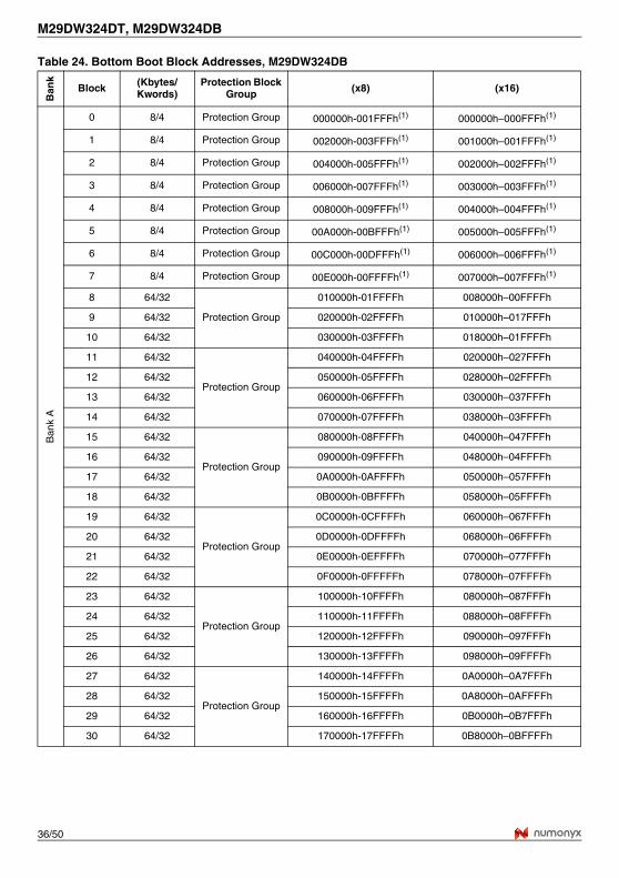
M29DW324DT, M29DW324DB
36/50
Table 24. Bottom Boot Block Addresses, M29DW324DBB
ank
Block (Kbytes/Kwords)
Protection Block Group (x8) (x16)
Ban
k A
0 8/4 Protection Group 000000h-001FFFh(1) 000000h–000FFFh(1)
1 8/4 Protection Group 002000h-003FFFh(1) 001000h–001FFFh(1)
2 8/4 Protection Group 004000h-005FFFh(1) 002000h–002FFFh(1)
3 8/4 Protection Group 006000h-007FFFh(1) 003000h–003FFFh(1)
4 8/4 Protection Group 008000h-009FFFh(1) 004000h–004FFFh(1)
5 8/4 Protection Group 00A000h-00BFFFh(1) 005000h–005FFFh(1)
6 8/4 Protection Group 00C000h-00DFFFh(1) 006000h–006FFFh(1)
7 8/4 Protection Group 00E000h-00FFFFh(1) 007000h–007FFFh(1)
8 64/32
Protection Group
010000h-01FFFFh 008000h–00FFFFh
9 64/32 020000h-02FFFFh 010000h–017FFFh
10 64/32 030000h-03FFFFh 018000h–01FFFFh
11 64/32
Protection Group
040000h-04FFFFh 020000h–027FFFh
12 64/32 050000h-05FFFFh 028000h–02FFFFh
13 64/32 060000h-06FFFFh 030000h–037FFFh
14 64/32 070000h-07FFFFh 038000h–03FFFFh
15 64/32
Protection Group
080000h-08FFFFh 040000h–047FFFh
16 64/32 090000h-09FFFFh 048000h–04FFFFh
17 64/32 0A0000h-0AFFFFh 050000h–057FFFh
18 64/32 0B0000h-0BFFFFh 058000h–05FFFFh
19 64/32
Protection Group
0C0000h-0CFFFFh 060000h–067FFFh
20 64/32 0D0000h-0DFFFFh 068000h–06FFFFh
21 64/32 0E0000h-0EFFFFh 070000h–077FFFh
22 64/32 0F0000h-0FFFFFh 078000h–07FFFFh
23 64/32
Protection Group
100000h-10FFFFh 080000h–087FFFh
24 64/32 110000h-11FFFFh 088000h–08FFFFh
25 64/32 120000h-12FFFFh 090000h–097FFFh
26 64/32 130000h-13FFFFh 098000h–09FFFFh
27 64/32
Protection Group
140000h-14FFFFh 0A0000h–0A7FFFh
28 64/32 150000h-15FFFFh 0A8000h–0AFFFFh
29 64/32 160000h-16FFFFh 0B0000h–0B7FFFh
30 64/32 170000h-17FFFFh 0B8000h–0BFFFFh

37/50
M29DW324DT, M29DW324DB
Ban
k A
31 64/32
Protection Group
180000h-18FFFFh 0C0000h–0C7FFFh
32 64/32 190000h-19FFFFh 0C8000h–0CFFFFh
33 64/32 1A0000h-1AFFFFh 0D0000h–0D7FFFh
34 64/32 1B0000h-1BFFFFh 0D8000h–0DFFFFh
35 64/32
Protection Group
1C0000h-1CFFFFh 0E0000h–0E7FFFh
36 64/32 1D0000h-1DFFFFh 0E8000h–0EFFFFh
37 64/32 1E0000h-1EFFFFh 0F0000h–0F7FFFh
38 64/32 1F0000h-1FFFFFh 0F8000h–0FFFFFh
Ban
k B
39 64/32
Protection Group
200000h-20FFFFh 100000h–107FFFh
40 64/32 210000h-21FFFFh 108000h–10FFFFh
41 64/32 220000h-22FFFFh 110000h–117FFFh
42 64/32 230000h-23FFFFh 118000h–11FFFFh
43 64/32
Protection Group
240000h-24FFFFh 120000h–127FFFh
44 64/32 250000h-25FFFFh 128000h–12FFFFh
45 64/32 260000h-26FFFFh 130000h–137FFFh
46 64/32 270000h-27FFFFh 138000h–13FFFFh
47 64/32
Protection Group
280000h-28FFFFh 140000h–147FFFh
48 64/32 290000h-29FFFFh 148000h–14FFFFh
49 64/32 2A0000h-2AFFFFh 150000h–157FFFh
50 64/32 2B0000h-2BFFFFh 158000h–15FFFFh
51 64/32
Protection Group
2C0000h-2CFFFFh 160000h–167FFFh
52 64/32 2D0000h-2DFFFFh 168000h–16FFFFh
53 64/32 2E0000h-2EFFFFh 170000h–177FFFh
54 64/32 2F0000h-2FFFFFh 178000h–17FFFFh
55 64/32
Protection Group
300000h-30FFFFh 180000h–187FFFh
56 64/32 310000h-31FFFFh 188000h–18FFFFh
57 64/32 320000h-32FFFFh 190000h–197FFFh
58 64/32 330000h-33FFFFh 198000h–19FFFFh
59 64/32
Protection Group
340000h-34FFFFh 1A0000h–1A7FFFh
60 64/32 350000h-35FFFFh 1A8000h–1AFFFFh
61 64/32 360000h-36FFFFh 1B0000h–1B7FFFh
62 64/32 370000h-37FFFFh 1B8000h–1BFFFFh
Ban
k
Block (Kbytes/Kwords)
Protection Block Group (x8) (x16)

M29DW324DT, M29DW324DB
38/50
Note: 1. Used as the Extended Block Addresses in Extended Block mode.
Ban
k B
63 64/32
Protection Group
380000h-38FFFFh 1C0000h–1C7FFFh
64 64/32 390000h-39FFFFh 1C8000h–1CFFFFh
65 64/32 3A0000h-3AFFFFh 1D0000h–1D7FFFh
66 64/32 3B0000h-3BFFFFh 1D8000h–1DFFFFh
67 64/32
Protection Group
3C0000h-3CFFFFh 1E0000h–1E7FFFh
68 64/32 3D0000h-3DFFFFh 1E8000h–1EFFFFh
69 64/32 3E0000h-3EFFFFh 1F0000h–1F7FFFh
70 64/32 Protection Group 3F0000h-3FFFFFh 1F8000h–1FFFFFh
Ban
k
Block (Kbytes/Kwords)
Protection Block Group (x8) (x16)

39/50
M29DW324DT, M29DW324DB
APPENDIX B. COMMON FLASH INTERFACE (CFI) The Common Flash Interface is a JEDEC ap-proved, standardized data structure that can beread from the Flash memory device. It allows asystem software to query the device to determinevarious electrical and timing parameters, densityinformation and functions supported by the mem-ory. The system can interface easily with the de-vice, enabling the software to upgrade itself whennecessary.When the CFI Query Command is issued the de-vice enters CFI Query mode and the data structure
is read from the memory. Tables 25, 26, 27, 28, 29and 30 show the addresses used to retrieve thedata.The CFI data structure also contains a securityarea where a 64 bit unique security number is writ-ten (see Table 30., Security Code Area). This areacan be accessed only in Read mode by the finaluser. It is impossible to change the security num-ber after it has been written by Numonyx.
Table 25. Query Structure Overview
Note: Query data are always presented on the lowest order data outputs.
Table 26. CFI Query Identification String
Note: Query data are always presented on the lowest order data outputs (DQ7-DQ0) only. DQ8-DQ15 are ‘0’.
AddressSub-section Name Description
x16 x8
10h 20h CFI Query Identification String Command set ID and algorithm data offset
1Bh 36h System Interface Information Device timing & voltage information
27h 4Eh Device Geometry Definition Flash device layout
40h 80h Primary Algorithm-specific Extended Query table
Additional information specific to the Primary Algorithm (optional)
61h C2h Security Code Area 64 bit unique device number
AddressData Description Value
x16 x8
10h 20h 0051h “Q”
11h 22h 0052h Query Unique ASCII String "QRY" "R"
12h 24h 0059h "Y"
13h 26h 0002h Primary Algorithm Command Set and Control Interface ID code 16 bit ID code defining a specific algorithm
AMDCompatible14h 28h 0000h
15h 2Ah 0040hAddress for Primary Algorithm extended Query table (see Table 29.) P = 40h
16h 2Ch 0000h
17h 2Eh 0000h Alternate Vendor Command Set and Control Interface ID Code second vendor - specified algorithm supported NA
18h 30h 0000h
19h 32h 0000h Address for Alternate Algorithm extended Query table NA1Ah 34h 0000h

M29DW324DT, M29DW324DB
40/50
Table 27. CFI Query System Interface Information
Table 28. Device Geometry Definition
Note: For the M29DW324DB, Region 1 corresponds to addresses 000000h to 007FFFh and Region 2 to addresses 008000h to 1FFFFFh.For the M29DW324DT, Region 1 corresponds to addresses 1F8000h to 1FFFFFh and Region 2 to addresses 000000h to 1F7FFFh.
AddressData Description Value
x16 x8
1Bh 36h 0027hVCC Logic Supply Minimum Program/Erase voltage
bit 7 to 4BCD value in voltsbit 3 to 0BCD value in 100 mV
2.7V
1Ch 38h 0036hVCC Logic Supply Maximum Program/Erase voltage
bit 7 to 4BCD value in voltsbit 3 to 0BCD value in 100 mV
3.6V
1Dh 3Ah 00B5hVPP [Programming] Supply Minimum Program/Erase voltage
bit 7 to 4HEX value in voltsbit 3 to 0BCD value in 100 mV
11.5V
1Eh 3Ch 00C5hVPP [Programming] Supply Maximum Program/Erase voltage
bit 7 to 4HEX value in voltsbit 3 to 0BCD value in 100 mV
12.5V
1Fh 3Eh 0004h Typical timeout per single byte/word program = 2n µs 16µs
20h 40h 0000h Typical timeout for minimum size write buffer program = 2n µs NA
21h 42h 000Ah Typical timeout per individual block erase = 2n ms 1s
22h 44h 0000h Typical timeout for full Chip Erase = 2n ms NA
23h 46h 0004h Maximum timeout for byte/word program = 2n times typical 256 µs
24h 48h 0000h Maximum timeout for write buffer program = 2n times typical NA
25h 4Ah 0003h Maximum timeout per individual block erase = 2n times typical 8 s
26h 4Ch 0000h Maximum timeout for Chip Erase = 2n times typical NA
AddressData Description Value
x16 x8
27h 4Eh 0016h Device Size = 2n in number of bytes 4 MByte
28h29h
50h52h
0002h0000h Flash Device Interface Code description x8, x16
Async.
2Ah2Bh
54h56h
0000h0000h Maximum number of bytes in multi-byte program or page = 2n NA
2Ch 58h 0002h Number of Erase Block Regions. It specifies the number of regions containing contiguous Erase Blocks of the same size. 2
2Dh 2Eh
5Ah5Ch
0007h0000h
Region 1 InformationNumber of Erase Blocks of identical size = 0007h+1 8
2Fh 30h
5Eh60h
0020h0000h
Region 1 InformationBlock size in Region 1 = 0020h * 256 byte 8Kbyte
31h 32h
62h64h
003Eh0000h
Region 2 InformationNumber of Erase Blocks of identical size = 003Eh+1 63
33h 34h
66h68h
0000h0001h
Region 2 InformationBlock size in Region 2 = 0100h * 256 byte 64Kbyte

41/50
M29DW324DT, M29DW324DB
Table 29. Primary Algorithm-Specific Extended Query Table
Table 30. Security Code Area
AddressData Description Value
x16 x8
40h 80h 0050h
Primary Algorithm extended Query table unique ASCII string “PRI”
"P"
41h 82h 0052h "R"
42h 84h 0049h "I"
43h 86h 0031h Major version number, ASCII "1"
44h 88h 0030h Minor version number, ASCII "0"
45h 8Ah 0000h Address Sensitive Unlock (bits 1 to 0)00 = required, 01= not requiredSilicon Revision Number (bits 7 to 2)
Yes
46h 8Ch 0002h Erase Suspend00 = not supported, 01 = Read only, 02 = Read and Write
2
47h 8Eh 0001h Block Protection 00 = not supported, x = number of blocks in per group
1
48h 90h 0001h Temporary Block Unprotect 00 = not supported, 01 = supported
Yes
49h 92h 0004h Block Protect /Unprotect04 = M29DW324D
04
4Ah 94h 0020h Simultaneous Operations, x = number of blocks in Bank B
32
4Bh 96h 0000h Burst Mode, 00 = not supported, 01 = supported No
4Ch 98h 0000h Page Mode, 00 = not supported, 01 = 4 page word, 02 = 8 page word No
4Dh 9Ah 00B5h VPP Supply Minimum Program/Erase voltagebit 7 to 4 HEX value in voltsbit 3 to 0 BCD value in 100 mV
11.5V
4Eh 9Ch 00C5h VPP Supply Maximum Program/Erase voltagebit 7 to 4 HEX value in voltsbit 3 to 0 BCD value in 100 mV
12.5V
4Fh 9Eh 000xh Top/Bottom Boot Block Flag02h = Bottom Boot device, 03h = Top Boot device
–
AddressData Description
x16 x8
61h C3h, C2h XXXX
64 bit: unique device number62h C5h, C4h XXXX
63h C7h, C6h XXXX
64h C9h, C8h XXXX
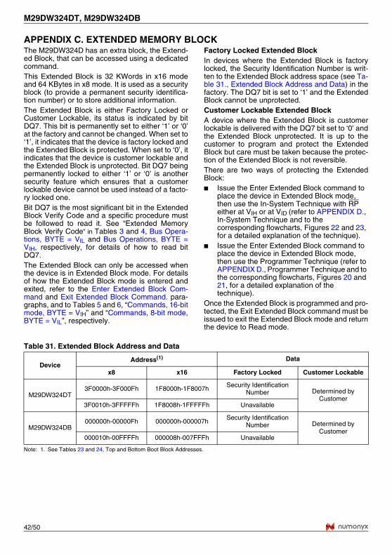
M29DW324DT, M29DW324DB
42/50
APPENDIX C. EXTENDED MEMORY BLOCKThe M29DW324D has an extra block, the Extend-ed Block, that can be accessed using a dedicatedcommand.This Extended Block is 32 KWords in x16 modeand 64 KBytes in x8 mode. It is used as a securityblock (to provide a permanent security identifica-tion number) or to store additional information. The Extended Block is either Factory Locked orCustomer Lockable, its status is indicated by bitDQ7. This bit is permanently set to either ‘1’ or ‘0’at the factory and cannot be changed. When set to‘1’, it indicates that the device is factory locked andthe Extended Block is protected. When set to ‘0’, itindicates that the device is customer lockable andthe Extended Block is unprotected. Bit DQ7 beingpermanently locked to either ‘1’ or ‘0’ is anothersecurity feature which ensures that a customerlockable device cannot be used instead of a facto-ry locked one.Bit DQ7 is the most significant bit in the ExtendedBlock Verify Code and a specific procedure mustbe followed to read it. See “Extended MemoryBlock Verify Code” in Tables 3 and 4, Bus Opera-tions, BYTE = VIL and Bus Operations, BYTE =VIH, respectively, for details of how to read bitDQ7.The Extended Block can only be accessed whenthe device is in Extended Block mode. For detailsof how the Extended Block mode is entered andexited, refer to the Enter Extended Block Com-mand and Exit Extended Block Command. para-graphs, and to Tables 5 and 6, “Commands, 16-bitmode, BYTE = VIH” and “Commands, 8-bit mode,BYTE = VIL”, respectively.
Factory Locked Extended BlockIn devices where the Extended Block is factorylocked, the Security Identification Number is writ-ten to the Extended Block address space (see Ta-ble 31., Extended Block Address and Data) in thefactory. The DQ7 bit is set to ‘1’ and the ExtendedBlock cannot be unprotected.Customer Lockable Extended BlockA device where the Extended Block is customerlockable is delivered with the DQ7 bit set to ‘0’ andthe Extended Block unprotected. It is up to thecustomer to program and protect the ExtendedBlock but care must be taken because the protec-tion of the Extended Block is not reversible.There are two ways of protecting the ExtendedBlock:■ Issue the Enter Extended Block command to
place the device in Extended Block mode, then use the In-System Technique with RP either at VIH or at VID (refer to APPENDIX D., In-System Technique and to the corresponding flowcharts, Figures 22 and 23, for a detailed explanation of the technique).
■ Issue the Enter Extended Block command to place the device in Extended Block mode, then use the Programmer Technique (refer to APPENDIX D., Programmer Technique and to the corresponding flowcharts, Figures 20 and 21, for a detailed explanation of the technique).
Once the Extended Block is programmed and pro-tected, the Exit Extended Block command must beissued to exit the Extended Block mode and returnthe device to Read mode.
Table 31. Extended Block Address and Data
Note: 1. See Tables 23 and 24, Top and Bottom Boot Block Addresses.
DeviceAddress(1) Data
x8 x16 Factory Locked Customer Lockable
M29DW324DT3F0000h-3F000Fh 1F8000h-1F8007h Security Identification
Number Determined by Customer
3F0010h-3FFFFFh 1F8008h-1FFFFFh Unavailable
M29DW324DB000000h-00000Fh 000000h-000007h Security Identification
Number Determined by Customer
000010h-00FFFFh 000008h-007FFFh Unavailable

43/50
M29DW324DT, M29DW324DB
APPENDIX D. BLOCK PROTECTIONBlock protection can be used to prevent any oper-ation from modifying the data stored in the memo-ry. The blocks are protected in groups, refer toAPPENDIX A., Tables 23 and 24 for details of theProtection Groups. Once protected, Program andErase operations within the protected group fail tochange the data.There are three techniques that can be used tocontrol Block Protection, these are the Program-mer technique, the In-System technique and Tem-porary Unprotection. Temporary Unprotection iscontrolled by the Reset/Block Temporary Unpro-tection pin, RP; this is described in the Signal De-scriptions section.To protect the Extended Block issue the Enter Ex-tended Block command and then use either theProgrammer or In-System technique. Once pro-tected issue the Exit Extended Block command toreturn to read mode. The Extended Block protec-tion is irreversible, once protected the protectioncannot be undone.Programmer TechniqueThe Programmer technique uses high (VID) volt-age levels on some of the bus pins. These cannotbe achieved using a standard microprocessor bus,therefore the technique is recommended only foruse in Programming Equipment.To protect a group of blocks follow the flowchart inFigure 20., Programmer Equipment Group ProtectFlowchart. To unprotect the whole chip it is neces-sary to protect all of the groups first, then allgroups can be unprotected at the same time. Tounprotect the chip follow Figure 21., ProgrammerEquipment Chip Unprotect Flowchart. Table 32.,
Programmer Technique Bus Operations, BYTE =VIH or VIL, gives a summary of each operation.The timing on these flowcharts is critical. Careshould be taken to ensure that, where a pause isspecified, it is followed as closely as possible. Donot abort the procedure before reaching the end.Chip Unprotect can take several seconds and auser message should be provided to show that theoperation is progressing.In-System TechniqueThe In-System technique requires a high voltagelevel on the Reset/Blocks Temporary Unprotectpin, RP(1). This can be achieved without violatingthe maximum ratings of the components on the mi-croprocessor bus, therefore this technique is suit-able for use after the memory has been fitted tothe system.To protect a group of blocks follow the flowchart inFigure 22., In-System Equipment Group ProtectFlowchart. To unprotect the whole chip it is neces-sary to protect all of the groups first, then all thegroups can be unprotected at the same time. Tounprotect the chip follow Figure 23., In-SystemEquipment Chip Unprotect Flowchart.The timing on these flowcharts is critical. Careshould be taken to ensure that, where a pause isspecified, it is followed as closely as possible. Donot allow the microprocessor to service interruptsthat will upset the timing and do not abort the pro-cedure before reaching the end. Chip Unprotectcan take several seconds and a user messageshould be provided to show that the operation isprogressing.Note: 1. RP can be either at VIH or at VID when using the In-Sys-
tem Technique to protect the Extended Block.
Table 32. Programmer Technique Bus Operations, BYTE = VIH or VIL
Note: 1. Block Protection Groups are shown in APPENDIX D., Tables 23 and 24.
Operation E G W Address InputsA0-A20
Data Inputs/OutputsDQ15A–1, DQ14-DQ0
Block (Group) Protect(1) VIL VID VIL Pulse A9 = VID, A12-A20 Block Address
Others = XX
Chip Unprotect VID VID VIL Pulse A9 = VID, A12 = VIH, A15 = VIH Others = X
X
Block (Group) Protection Verify
VIL VIL VIH
A0 = VIL, A1 = VIH, A6 = VIL, A9 = VID, A12-A20 Block Address
Others = X
Pass = XX01hRetry = XX00h
Block (Group) Unprotection Verify
VIL VIL VIH
A0 = VIL, A1 = VIH, A6 = VIH, A9 = VID, A12-A20 Block Address
Others = X
Retry = XX01hPass = XX00h

M29DW324DT, M29DW324DB
44/50
Figure 20. Programmer Equipment Group Protect Flowchart
Note: Block Protection Groups are shown in APPENDIX D., Tables 23 and 24.
ADDRESS = GROUP ADDRESS
AI05574
G, A9 = VID,E = VIL
n = 0
Wait 4µs
Wait 100µs
W = VIL
W = VIH
E, G = VIH,A0, A6 = VIL,
A1 = VIH
A9 = VIHE, G = VIH
++n= 25
START
FAIL
PASS
YES
NO
DATA=
01hYES
NO
W = VIH
E = VIL
Wait 4µs
G = VIL
Wait 60ns
Read DATA
Ver
ifyP
rote
ctS
et-u
pE
nd
A9 = VIHE, G = VIH

45/50
M29DW324DT, M29DW324DB
Figure 21. Programmer Equipment Chip Unprotect Flowchart
Note: Block Protection Groups are shown in APPENDIX D., Tables 23 and 24.
PROTECT ALL GROUPS
AI05575
A6, A12, A15 = VIH(1)
E, G, A9 = VID
DATA
W = VIH
E, G = VIH
ADDRESS = CURRENT GROUP ADDRESSA0 = VIL, A1, A6 = VIH
Wait 10ms
=00h
INCREMENTCURRENT GROUP
n = 0CURRENT GROUP = 0
Wait 4µs
W = VIL
++n= 1000
START
YES
YESNO
NO LASTGROUP
YES
NO
E = VIL
Wait 4µs
G = VIL
Wait 60ns
Read DATA
FAIL PASS
Ver
ifyU
npro
tect
Set
-up
End
A9 = VIHE, G = VIH
A9 = VIHE, G = VIH

M29DW324DT, M29DW324DB
46/50
Figure 22. In-System Equipment Group Protect Flowchart
Note: 1. Block Protection Groups are shown in APPENDIX D., Tables 23 and 24.2. RP can be either at VIH or at VID when using the In-System Technique to protect the Extended Block.
AI05576
WRITE 60hADDRESS = GROUP ADDRESS
A0 = VIL, A1 = VIH, A6 = VIL
n = 0
Wait 100µs
WRITE 40hADDRESS = GROUP ADDRESS
A0 = VIL, A1 = VIH, A6 = VIL
RP = VIH++n= 25
START
FAIL
PASS
YES
NO
DATA=
01hYES
NO
RP = VIH
Wait 4µs
Ver
ifyP
rote
ctS
et-u
pE
nd
READ DATAADDRESS = GROUP ADDRESS
A0 = VIL, A1 = VIH, A6 = VIL
RP = VID
ISSUE READ/RESETCOMMAND
ISSUE READ/RESETCOMMAND
WRITE 60hADDRESS = GROUP ADDRESS
A0 = VIL, A1 = VIH, A6 = VIL

47/50
M29DW324DT, M29DW324DB
Figure 23. In-System Equipment Chip Unprotect Flowchart
Note: Block Protection Groups are shown in APPENDIX D., Tables 23 and 24.
AI05577
WRITE 60hANY ADDRESS WITH
A0 = VIL, A1 = VIH, A6 = VIH
n = 0CURRENT GROUP = 0
Wait 10ms
WRITE 40hADDRESS = CURRENT GROUP ADDRESS
A0 = VIL, A1 = VIH, A6 = VIH
RP = VIH
++n= 1000
START
FAIL PASS
YES
NO
DATA=
00h
YESNO
RP = VIH
Wait 4µs
READ DATAADDRESS = CURRENT GROUP ADDRESS
A0 = VIL, A1 = VIH, A6 = VIH
RP = VID
ISSUE READ/RESETCOMMAND
ISSUE READ/RESETCOMMAND
PROTECT ALL GROUPS
INCREMENTCURRENT GROUP
LASTGROUP
YES
NO
WRITE 60hANY ADDRESS WITH
A0 = VIL, A1 = VIH, A6 = VIH
Ver
ifyU
npro
tect
Set
-up
End
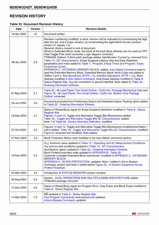
M29DW324DT, M29DW324DB
48/50
REVISION HISTORY
Table 33. Document Revision History
Date Version Revision Details
19-Apr-2002 -01 Document written
08-Apr-2003 2.0
Revision numbering modified: a minor revision will be indicated by incrementing the digit after the dot, and a major revision, by incrementing the digit before the dot (revision version 01 equals 1.0).Revision History moved to end of document.When in Extended Block mode, the block at the boot block address can be used as OTP. Data Toggle Flow chart corrected. Logic diagram corrected.TFBGA48, 6x8mm, 0.8mm pitch package added. Identification Current IID removed from Table 14., DC Characteristics. Erase Suspend Latency time and Data Retention parameters and notes added to Table 7., Program, Erase Times and Program, Erase Endurance Cycles.APPENDIX C., EXTENDED MEMORY BLOCK, added. Auto Select Command sued to read the Extended Memory Block. Extended Memory Block Verify Code row added to Tables 3 and 4, Bus Operations, BYTE = VIL and Bus Operations, BYTE = VIH. Bank Address modified in Auto Select Command. Chip Erase Address modified in Table 8., Status Register Bits. VSS pin connection to ground clarified. Note added to Table 22., Ordering Information Scheme.
07-May-2003 2.1Table 20., 48 Lead Plastic Thin Small Outline, 12x20 mm, Package Mechanical Data and Figure 18., 48 Lead Plastic Thin Small Outline, 12x20 mm, Bottom View Package Outline” corrected.
25-Jun-2003 3.0 Document promoted from Preliminary Data to full Datasheet status. Packing option added to Table 22., Ordering Information Scheme.
18-Sep-2003 3.1
Status of Ready/Busy signal for Erase Suspend Operation modified in Table 8., Status Register Bits.Figures 14 and 15, Toggle and Alternative Toggle Bits Mechanisms added.Table 18., Toggle and Alternative Toggle Bits AC Characteristics, added.Note 1 of Table 28., Device Geometry Definition, modified.
07-Oct-2003 3.2Figures 14 and 15, Toggle and Alternative Toggle Bits Mechanisms modified and Notes 1 and 2 added. Table 18., Toggle and Alternative Toggle Bits AC Characteristics, modified.Figure 8. renamed and modified; Note added.
07-Nov-2003 3.3 Block Protection Status read modified in the Auto Select command section.
19-Dec-2003 3.4
VCC minimum value updated in Table 12., Operating and AC Measurement Conditions. VPP and IPP test conditions updated in Table 14., DC Characteristics.Architecture option updated in Table 22., Ordering Information Scheme. Block Protect/Unprotect code updated in APPENDIX B., Table 29.Customer Lockable Extended Block mechanism modified in APPENDIX C., EXTENDED MEMORY BLOCK. APPENDIX D., BLOCK PROTECTION, updated: Note 1 added in the In-System Technique section and Note 2 added below Figure 22., In-System Equipment Group Protect Flowchart.
23-Mar-2004 4.0 Introduction of STATUS REGISTER section clarified.
30-Aug-2004 5.0 Section , DUAL OPERATIONS AND MULTIPLE BANK ARCHITECTURE added.TFBGA63 package removed.
10-Dec-2004 6.0 Status of Ready/Busy signal for Program Error, Chip Erase and Block Erase modified in Table 8., Status Register Bits.
14-Mar-2004 7.0RB updated in Table 8., Status Register Bits.Fast Program Commands restructured and updated. Unlock Bypass Command. updated.

49/50
M29DW324DT, M29DW324DB
27-Mar-2008 8.0 Applied Numonyx branding.
Date Version Revision Details

M29DW324DT, M29DW324DB
50/50
Please Read Carefully:
INFORMATION IN THIS DOCUMENT IS PROVIDED IN CONNECTION WITH NUMONYX™ PRODUCTS. NO LICENSE, EXPRESS OR IMPLIED, BY ESTOPPEL OR OTHERWISE, TO ANY INTELLECTUAL PROPERTY RIGHTS IS GRANTED BY THIS DOCUMENT. EXCEPT AS PROVIDED IN NUMONYX'S TERMS AND CONDITIONS OF SALE FOR SUCH PRODUCTS, NUMONYX ASSUMES NO LIABILITY
WHATSOEVER, AND NUMONYX DISCLAIMS ANY EXPRESS OR IMPLIED WARRANTY, RELATING TO SALE AND/OR USE OF NUMONYX PRODUCTS INCLUDING LIABILITY OR WARRANTIES RELATING TO FITNESS FOR A PARTICULAR PURPOSE, MERCHANTABILITY, OR INFRINGEMENT OF ANY PATENT, COPYRIGHT OR OTHER INTELLECTUAL PROPERTY RIGHT.
Numonyx products are not intended for use in medical, life saving, life sustaining, critical control or safety systems, or in nuclear facility applications.
Numonyx may make changes to specifications and product descriptions at any time, without notice.
Numonyx, B.V. may have patents or pending patent applications, trademarks, copyrights, or other intellectual property rights that relate to the presented subject matter. The furnishing of documents and other materials and information does not provide any license, express or
implied, by estoppel or otherwise, to any such patents, trademarks, copyrights, or other intellectual property rights.
Designers must not rely on the absence or characteristics of any features or instructions marked “reserved” or “undefined.” Numonyx reserves these for future definition and shall have no responsibility whatsoever for conflicts or incompatibilities arising from future changes to them.
Contact your local Numonyx sales office or your distributor to obtain the latest specifications and before placing your product order.
Copies of documents which have an order number and are referenced in this document, or other Numonyx literature may be obtained by visiting Numonyx's website at http://www.numonyx.com.
Numonyx StrataFlash is a trademark or registered trademark of Numonyx or its subsidiaries in the United States and other countries.
*Other names and brands may be claimed as the property of others.
Copyright © 11/5/7, Numonyx, B.V., All Rights Reserved.