32-bit risc microcontroller tmpm4g group(1)
TRANSCRIPT

TMPM4G Group(1)
Clock Control and Operation Mode
2018-04-03 1 / 53 Rev. 2.0
© 2018 Toshiba Electronic Devices & Storage Corporation
2018-04
32-bit RISC microcontroller
TMPM4G Group(1)
Reference Manual Clock Control and Operation Mode
(CG-M4G(1)-C)
Revision 2.0
TMPM4G Group(1)
Clock Control and Operation Mode
2018-04-03 2 / 53 Rev. 2.0
Contents
Preface .............................................................................................................................................................. 5
Related document ..................................................................................................................................................... 5
Conventions .............................................................................................................................................................. 6
Terms and Abbreviations .......................................................................................................................................... 8
1. Outlines ...................................................................................................................................................... 9
2. Clock control ............................................................................................................................................ 10
Clock type ........................................................................................................................................................ 10 2.1.
The initial value by a reset action .................................................................................................................... 10 2.2.
Clock System diagram ..................................................................................................................................... 11 2.3.
Warming up function ........................................................................................................................................ 12 2.4.2.4.1. The warming up counter for a high speed oscillation .................................................................................................. 12 2.4.2. The warming up counter for a low speed oscillation ................................................................................................... 13 2.4.3. The directions for a warming up timer ........................................................................................................................ 13
Clock multiplying circuit (PLL) for fsys ............................................................................................................. 14 2.5.2.5.1. A PLL setup after reset release .................................................................................................................................. 14 2.5.2. The formula and the example of a setting of a PLL multiplication value ..................................................................... 14 2.5.3. Change of the PLL multiplication value under operation ............................................................................................ 15 2.5.4. PLL operation start / stop / switching procedure ......................................................................................................... 16
2.5.4.1. fc setup (PLL stop >>> PLL start) .................................................................................................................................... 16 2.5.4.2. fc setup (conduct PLL >>> PLL stop) ............................................................................................................................... 16
System clock .................................................................................................................................................... 17 2.6.2.6.1. The setting method of a system clock ........................................................................................................................ 18
2.6.1.1. fosc setup (Internal oscillation >>> External oscillation) .................................................................................................. 18 2.6.1.2. fosc setup (Internal oscillation >>> External clock input) ................................................................................................. 19 2.6.1.3. fosc setup (External oscillation/External clock input >>> Internal oscillation).................................................................. 19
Low speed clock .............................................................................................................................................. 20 2.7.2.7.1. ELOSC Setting (No Operation of External Low Speed Oscillator >>> Operation) ...................................................... 20 2.7.2. ELCLKIN Setting (No Operation of External Low Speed Oscillator >>> Operation) ................................................... 20
Clock supply setting function ........................................................................................................................... 20 2.8.
Prescaler clock ................................................................................................................................................. 21 2.9.
3. Operation mode ....................................................................................................................................... 22
Details of an Operation mode .......................................................................................................................... 22 3.1.3.1.1. The feature in each mode ........................................................................................................................................... 22 3.1.2. Transition to and Return from Low Power Consumption mode .................................................................................. 23 3.1.3. Selection of a Low Power Consumption mode ........................................................................................................... 23 3.1.4. The peripheral function state in a Low Power Consumption mode ............................................................................. 24
Switch to and return from a Low Power Consumption mode .......................................................................... 26 3.2.3.2.1. IDLE mode transition flow ........................................................................................................................................... 26 3.2.2. STOP1 mode transition flow ....................................................................................................................................... 27 3.2.3. STOP2 mode transition flow ....................................................................................................................................... 28
Return from a Low Power Consumption mode ................................................................................................ 29 3.3.
TMPM4G Group(1)
Clock Control and Operation Mode
2018-04-03 3 / 53 Rev. 2.0
3.3.1. The release source of a Low Power Consumption mode ........................................................................................... 29 3.3.2. Warming up at the release of Low Power Consumption mode ................................................................................... 30 3.3.3. Restart operation from STOP2 mode ......................................................................................................................... 31
Clock operation by mode transition ................................................................................................................. 32 3.4.3.4.1. NORMAL >>> IDLE >>> NORMAL Operation mode transition .................................................................................. 32 3.4.2. NORMAL >>> STOP1 >>> NORMAL Operation mode transition ............................................................................... 32 3.4.3. NORMAL >>> STOP2 >>> RESET >>> NORMAL Operation mode transition .......................................................... 33
4. Explanation of a register .......................................................................................................................... 34
Register list ...................................................................................................................................................... 34 4.1.
Detail of Register ............................................................................................................................................. 35 4.2.4.2.1. [CGPROTECT] (CG write protection register) ............................................................................................................ 35 4.2.2. [CGOSCCR] (Oscillation control register) ................................................................................................................... 35 4.2.3. [CGSYSCR] (System clock control register) ............................................................................................................... 36 4.2.4. [CGSTBYCR] (Standby control register) .................................................................................................................... 37 4.2.5. [CGPLL0SEL] (PLL selection register for fsys) ........................................................................................................... 37 4.2.6. [CGWUPHCR] (High speed oscillation warming up register) ..................................................................................... 38 4.2.7. [CGWUPLCR] (Low speed oscillation warming up register) ....................................................................................... 39 4.2.8. [CGFSYSMENA] (Middle speed clock supply and stop register A for fsys) ................................................................ 40 4.2.9. [CGFSYSMENB] (Middle speed clock supply and stop register B for fsys) ................................................................ 42 4.2.10. [CGFSYSENA] (High speed clock supply and stop register A for fsys) .................................................................... 44 4.2.11. [CGFCEN] (Clock supply and stop register for fc) .................................................................................................... 45 4.2.12. [CGSPCLKEN] (Clock supply for ADC and Trace Register) ..................................................................................... 45 4.2.13. [CGEXTEND2] (Function extension register 2) ........................................................................................................ 46 4.2.14. [RLMLOSCCR] (Low speed oscillation and Internal High speed oscillation 2 clock control register) ....................... 47 4.2.15. [RLMSHTDNOP]( Power supply cut off control register) .......................................................................................... 47 4.2.16. [RLMPROTECT](RLM write protection register) ....................................................................................................... 47
5. Information according to product .............................................................................................................. 48
5.1. [CGFSYSENA] ................................................................................................................................................. 48
5.2. [CGFSYSMENA] .............................................................................................................................................. 49
5.3. [CGFSYSMENB] .............................................................................................................................................. 50
5.4. [CGFCEN] ........................................................................................................................................................ 51
6. Revision history ........................................................................................................................................ 52
RESTRICTIONS ON PRODUCT USE ............................................................................................................ 53

TMPM4G Group(1)
Clock Control and Operation Mode
2018-04-03 4 / 53 Rev. 2.0
List of Figure
Figure 2.1 Clock system diagram .......................................................................................................... 11 Figure 3.1 Change state ........................................................................................................................ 26 Figure 3.2 STOP2 mode restart operation flow ..................................................................................... 31 Figure 3.3 NORMAL >>> STOP1 >>> NORMAL Operation mode transition ........................................ 32 Figure 3.4 NORMAL >>> STOP2 >>> RESET >>> NORMAL Operation mode transition .................... 33
List of Tables Table 2.1 Details of a [CGPLL0SEL] <PLL0SET [23:0]>setup .............................................................. 14 Table 2.2 PLL correction (example) ....................................................................................................... 15 Table 2.3 PLL0SET setting value (example) ......................................................................................... 15 Table 2.4 Clock domains of CPU and peripherals ................................................................................. 17 Table 2.5 Time interval for changing System clock ............................................................................... 17 Table 2.6 Example of operation frequency (unit: MHz) .......................................................................... 18 Table 2.7 Operating frequency examples of High speed and Middle speed system clocks .................. 18 Table 2.8 Time interval for changing prescaler clocks ........................................................................... 21 Table 3.1 Low Power Consumption mode selection .............................................................................. 23 Table 3.2 Block operation status in each Low Power Consumption mode ............................................ 24 Table 3.3 Release source list ................................................................................................................ 29 Table 3.4 Warming up ........................................................................................................................... 30 Table 5.1 [CGFSYSENA] register corresponding to each product ........................................................ 48 Table 5.2 [CGFSYSMENA] register corresponding to each product ..................................................... 49 Table 5.3 [CGFSYSMENB] register corresponding to each product ..................................................... 50 Table 5.4 [CGFCEN] register corresponding to each product ............................................................... 51 Table 6.1 Revision history ..................................................................................................................... 52

TMPM4G Group(1)
Clock Control and Operation Mode
2018-04-03 5 / 53 Rev. 2.0
Preface
Related document
Document name Exception Input/Output Ports Power Supply and Reset Operation Multi-function DMA controller

TMPM4G Group(1)
Clock Control and Operation Mode
2018-04-03 6 / 53 Rev. 2.0
Conventions ● Numeric formats follow the rules as shown below:
Hexadecimal: 0xABC Decimal: 123 or 0d123 – Only when it needs to be explicitly shown that they are decimal numbers. Binary: 0b111 – It is possible to omit the “0b” when the number of bit can be distinctly understood from a sentence.
● “_N” is added to the end of signal names to indicate low active signals. ● It is called “assert” that a signal moves to its active level, “deassert” to its inactive level. ● When two or more signal names are referred, they are described like as [m: n].
Example: S[3: 0] shows four signal names S3, S2, S1 and S0 together. ● The characters surrounded by [ ] defines the register.
Example: [ABCD] ● “n” substitutes suffix number of two or more same kind of registers, fields, and bit names.
Example: [XYZ1], [XYZ2], [XYZ3] [XYZn] ● "x" substitutes suffix number or character of units and channels in the Register List.
In case of unit, “x” means A, B, and C … Example: [ADACR0], [ADBCR0], [ADCCR0] [ADxCR0] In case of channel, “x” means 0, 1, and 2… Example: [T32A0RUNA], [T32A1RUNA], [T32A2RUNA] [T32AxRUNA]
● The bit range of a register is written like as [m: n]. Example: Bit[3: 0] expresses the range of bit 3 to 0.
● The configuration value of a register is expressed by either the hexadecimal number or the binary number. Example: [ABCD]<EFG> = 0x01 (hexadecimal), [XYZn]<VW> = 1 (binary)
● Word and Byte represent the following bit length. Byte: 8 bits Half word: 16 bits Word: 32 bits Double word: 64 bits
● Properties of each bit in a register are expressed as follows: R: Read only W: Write only R/W: Read and Write are possible
● Unless otherwise specified, register access supports only word access. ● The register defined as reserved must not be rewritten. Moreover, do not use the read value. ● The value read from the bit having default value of "-" is unknown. ● When a register containing both of writable bits and read-only bits is written, read-only bits should be written
with their default value, In the cases that default is “-“, follow the definition of each register. ● Reserved bits of the Write-only register should be written with their default value. In the cases that default is
“-”, follow the definition of each register. ● Do not use read-modified-write processing to the register of a definition which is different by writing and
read out.

TMPM4G Group(1)
Clock Control and Operation Mode
2018-04-03 7 / 53 Rev. 2.0
The flash memory uses the Super Flash® technology under the license of Silicon Storage Technology, Inc. Super Flash® is registered trademark of Silicon Storage Technology, Inc. All other company names, product names, and service names mentioned herein may be trademarks of their respective companies.
*********************************************************************************************************************** Arm, Cortex and Thumb are registered trademarks of Arm Limited (or its subsidiaries) in the US
and/or elsewhere. All rights reserved. ***********************************************************************************************************************
TMPM4G Group(1)
Clock Control and Operation Mode
2018-04-03 8 / 53 Rev. 2.0
Terms and Abbreviations Some of abbreviations used in this document are as follows: ADC Analog to Digital Converter A-PMD Advanced Programmable Motor Control Circuit CG Clock control and Generations CEC Consumer Electronics Control DAC Digital to Analog Converter DNF Digital Noise Filter EBIF External Bus Interface ELOSC External Low speed Oscillator EHOSC External High speed Oscillator fsys frequency of SYSTEM Clock IHOSC Internal High Speed Oscillator INT Interrupt ISD Interval Sensing Detector I2C Inter-Integrated Circuit LTTMR Long Term Timer LVD Voltage Detection Circuit MDMA Multi-function Direct Memory Access NMI Non-Maskable Interrupt NBDIF Non Break Debug Interface OFD Oscillation Frequency Detector POR Power On Reset Circuit RMC Remote control Signal preprocessor RLM Reset LOSC<Low power> Manager RTC Real Time Clock SIWDT Clock Selective Watchdog Timer SMIF Serial Memory Interface TRGSEL Trigger Selection circuit TSPI Toshiba Serial Peripheral Interface T32A 32-bit Timer Event Counter UART Universal Asynchronous Receiver Transmitter

TMPM4G Group(1)
Clock Control and Operation Mode
2018-04-03 9 / 53 Rev. 2.0
1. Outlines The clock/mode control block can select a clock gear or prescaler clock and set the warm-up of oscillator. Furthermore, it has Normal mode and a low power consumption mode in order to reduce power consumption using mode transition.
There is the following as a function relevant to a clock. ● System clock control ● Prescaler clock control
TMPM4G Group(1)
Clock Control and Operation Mode
2018-04-03 10 / 53 Rev. 2.0
2. Clock control
Clock type 2.1.This section shows a list of clocks:
EHCLKIN : The high speed clock input from the external fOSC : A clock generated in the internal oscillation circuit or input from the X1 and X2 pins fPLL : A clock multiplied by PLL fc : A clock selected by [CGOSCCR] <OSCSEL> (High speed clock) ELCLKIN : The low speed clock input from the external fs : A clock output from an external low speed oscillator fsysh : A high speed system clock selected by [CGSYSCR]<GEAR[2:0] > fsysm : A middle speed system clock selected by [CGSYSCR]<GEAR[2:0] ><MCKSEL[1:0] > ΦT0h : A high speed clock selected by [CGSYSCR]<PRCK[3:0]> (High speed prescaler clock) ΦT0m : A middle speed clock selected by [CGSYSCR]<PRCK[3:0]> <MCKSEL[1:0] > (Middle speed
prescaler clock) fIHOSC1 : A clock generated with the internal high speed oscillator 1 fIHOSC2 : A clock generated with the internal high speed oscillator 2 ADCLK : A conversion clock for AD converter TRCLKIN : A clock for tracing facilities of a debugging circuit (ETM)
Note: The high speed system clock and the middle speed system clock are collectively called System clock
(fsys). And the high speed prescaler clock and the middle speed prescaler clock are collectively called Prescaler clock (ΦT0).
The initial value by a reset action 2.2.A clock setup is initialized by the following states by a reset action.
External high speed oscillator : Stop Internal high speed oscillator 1 : Oscillation Internal high speed oscillator 2 : Stop (Note) External low speed oscillator : Stop PLL (multiplying circuit) : Stop Gear clock : fc (no frequency dividing)
Note: The state after the initialization done by the reset from the pin depends on [RLMLOSCCR]<POSCEN> setting.

TMPM4G Group(1)
Clock Control and Operation Mode
2018-04-03 11 / 53 Rev. 2.0
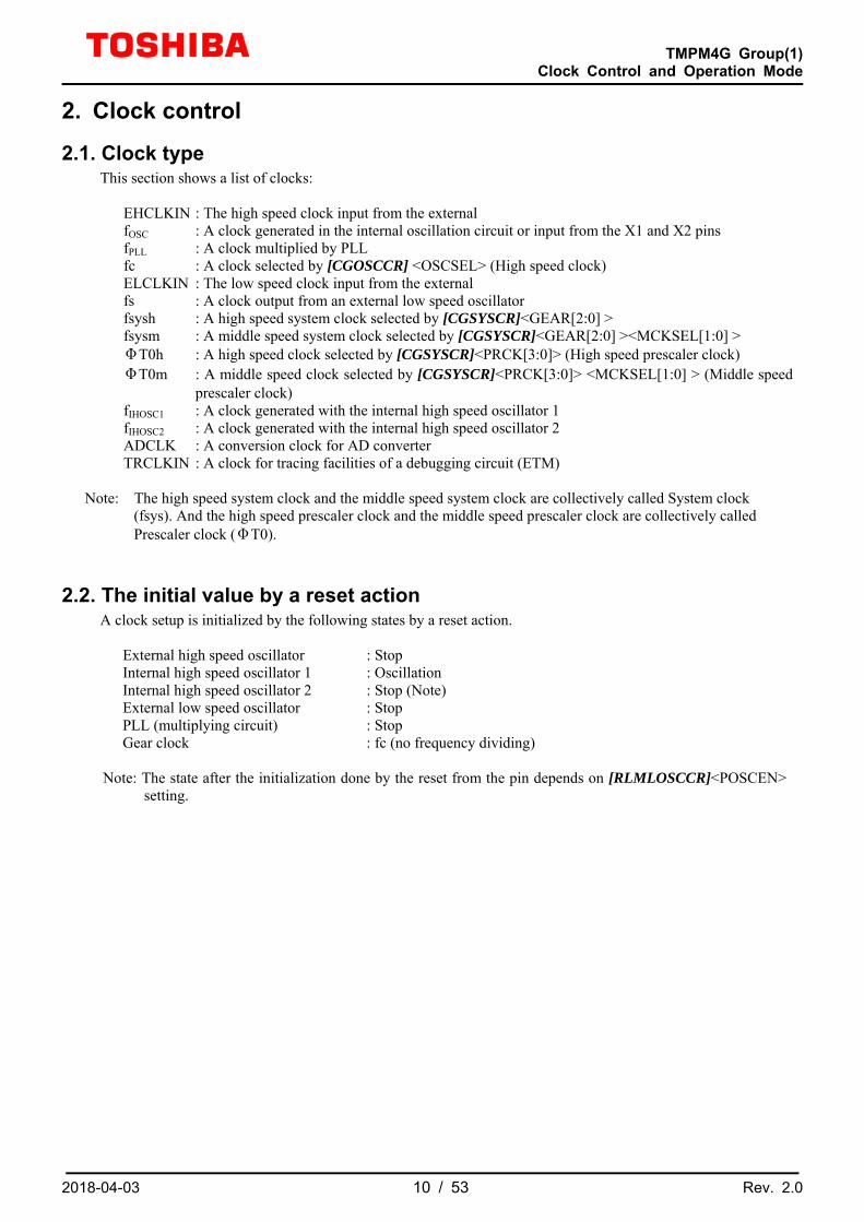
Clock System diagram 2.3.The figure below shows a clock system diagram.
Internal High speed ocillator1
External High speedoscillator1
X2
X1
[CGOSCCR]<EOSCEN[1:0]>After Reset: Stop fosc
[CGOSCCR]<IHOSC1EN>After Reset: Oscillation
fIHOSC1
[CGWUPHCR]<WUCLK>
High speedWarm up timer
[CGWUPHCR]<WUON>[CGWUPHCR]<WUPT[15:4]>
Internal High speed oscillator2
[RLMLOSCCR]<POSCEN>
After Reset: Stop(Note)
OFD
[CGOSCCR]<OSCSEL>
fpll
[CGPLL0SEL]<PLL0SEL>
ADC
External Low speed oscillator
XT2
XT1
Low speed Warm up timer
[CGWUPLCR]<WULON>[CGWUPLCR]<WUPTL[18:4]>
fs[Peripheral function clock inputs] RTC, ISD
fc
[Peripheral function prescaler inputs](High speed prescaler clock) TSPI0 to 5
[RLMLOSCCR ]<XTEN>
After Reset: Stop
[CGSYSCR]<PRCK[3:0]>
[CGSYSCR]<GEAR[2:0]>
[CGSPCLKEN]<TRCKEN>
1/64 SysTick
TRCK
1/64 1/1281/161/81/41/2 1/32 1/256 1/512
fc1/2
1/41/8
1/16
fosc
fsysh
Source clock control
[CGSPCLKEN]<ADCKEN>
EHCLKIN
fIHOSC2
fsysh
CPU
1/4
ELOSC
PLL0
[CGSYSCR]<MCKSEL[1:0]>
1/41/2
ΦT0m
1/41/2[CGFSYSMENA]
<IPMENAx>
[CGFSYSENA]<IPENAx>
ΦT0h
[Peripheral function prescaler inputs](Middle speed prescaler clock) FUART,UART, T32A TSPI6 to 8
fsysm UART, FUART, I2C, T32A, ADC, DAC, TSPI6 to 8, PMD, PORT, TRGSEL, OFD, NBD, SIWDT, TRM
[CGFSYSMENA]<IPMENAx>
[CGFSYSMENB]<IPMENBx>
CG, HDMAC,SMIF,EBIF,TSPI0 to 5,INT(IB)
[CGFSYSENA]<IPENAx>
fsyshfsysh
fsysh
fcDNF
DEBUG
ETMTRCLKIN
SIWDT
SIWDTFLASH
LTTMR
[Peripheral function clock inputs] RMC, CEC
MDMAC
[CGEXTEND2]<RSV22[2:0]>
MDMACSWRST
(High speed system clock)CPU, RAM0 to 2, BOOTROM, CodeFLASH, DataFLASH,
ELCLKIN
[RLMLOSCCR ]<DRCOSCL>
(Middle speed system clock) RAM3, BackupRAM, FLASH(SFR), LTTMR, RLM, INT(IA), RTC, ISD, RMC, CEC, LVD
ADCLK
[CGFCEN]<FCIPENx>
Note: The state after the initialization done by the reset from the pin depends on [RLMLOSCCR]<POSCEN> setting.
[CGFCEN]<FCIPEN23>
Figure 2.1 Clock system diagram

TMPM4G Group(1)
Clock Control and Operation Mode
2018-04-03 12 / 53 Rev. 2.0
Warming up function 2.4.A function for a warming up function to secure the oscillation stable time at the time of the STOP1 mode release which starts the warming up counter for high speed oscillator automatically. It is available also as a count-up timer which uses the exclusive warming up counter of high speed oscillator /low speed oscillator for the waiting for the stability of an external oscillator or an internal oscillator. This chapter explains the setting method to the register for warming up timers, and the case where it is used as a count-up timer. The detailed explanation at the time of STOP1 mode release, refer to "3.3.2Warming up at the release of Low Power Consumption mode".
2.4.1. The warming up counter for a high speed oscillation A 16-bit up-counter is built in as a warming up counter only for a high speed oscillation. Also when setting to the STOP1 mode before changes, it computes in the following formula, 4 bits of low ranks are omitted, and it sets to top 12 bits. A register will be set as [CGWUPHCR] <WUPT [15:4]>. 16 is subtracted in order to perform the count for 4 bits of low ranks, even when a set point is 0.
<Formula>
Warming up counter value (16 bits)
= (warming up time (s) / clock period (s)) - 16
(Example) When 5 ms of warming time is set up with 10 MHz (100 ns of clock periods) of oscillators Warming up counter value (16 bits) = (5ms / 100ns) - 16 = 50000 - 16 = 49984 = 0xC340
Since top 12 bits is set up, it sets to a register as follows. [CGWUPHCR]<WUPT[15:4]> = 0xC34
In the case of 10 MHz, the Setting range is 0 ≤ <WUPT[15:4]> ≤ 0xFFF, Warming up time is set to the value from 1.6 μs to 6.5536 ms.

TMPM4G Group(1)
Clock Control and Operation Mode
2018-04-03 13 / 53 Rev. 2.0
2.4.2. The warming up counter for a low speed oscillation A 19-bit rise counter is built in as a warming up counter only for a low speed oscillation. It computes in the following formula, 4 bits of low ranks are omitted, and it sets to top 15 bits. A register will be set as [CGWUPLCR] <WUPT [18:4]>. 16 is subtracted in order to perform the count for 4 bits of low ranks, even when a set point is 0.
<Formula>
Warming up counter value (19 bits)
= (warming up time (s) / clock period (s)) - 16
(Example) When 50 ms of warming time is set up with 32 kHz (clock period 31.25μs) of oscillators Warming up counter value (19 bits) = (50ms / 31.25μs) - 16 = 1600 - 16 = 1584 = 0x00630
Since top 15 bits is set up, it sets to a register as follows. [CGWUPLCR]<WUPTL[18:4]> = 0x0063
In the case of 32 kHz, it setting range is 0 ≤ <WUPTL[18:4]> ≤ 0x7FFF, Warming up time is set from 500μs to 16.384s.
2.4.3. The directions for a warming up timer The directions for a warming up function are explained. (1) Selection of a clock
In a high speed oscillation, the clock classification (an internal oscillation/external oscillation) counted at a warming up counter is chosen by [CGWUPHCR] <WUCLK>.
(2) Calculation of a warming up counter set value The warming up time can set any value to the counter for a high speed oscillation / for a low speed oscillation. Please compute and set up from each formula.
(3) The start of warming up, and a termination Confirmation When software (command) performs the start of warming up, and a termination Confirmation, a warming up count start is carried out by setting "1" to [CGWUPHCR] <WUON> (or [CGWUPLCR] <WULON>)]. Termination is [CGWUPHCR] <WUEF> (or [CGWUPLCR] <WULEF>). It distinguishes by becoming "1" to "0". "1" shows the inside of warming up and "0" shows termination. After a counting end, a counter is reset and returns to an initial state. It does not become forced termination although "0" is written in during counter operation to [CGWUPHCR] <WUON> (or [CGWUPLCR] <WULON>). "0" writing is disregarded.
Note1: Since it is operating with the oscillating clock, a warming up timer includes an error, when Oscillation frequency has fluctuation. Therefore, It serves as time of an outline.
TMPM4G Group(1)
Clock Control and Operation Mode
2018-04-03 14 / 53 Rev. 2.0
Clock multiplying circuit (PLL) for fsys 2.5.The clock multiplying circuit outputs the fPLL clock (maximum 160MHz) multiplied by the optimum condition for the frequency (8 MHz to 20 MHz) of the output clock fOSC of the high speed oscillator. So, it is possible to make input frequency to an oscillator low and to make an internal clock high speed by this circuit.
2.5.1. A PLL setup after reset release The PLL is disabled after reset release. In order to use the PLL, set a multiplication value to [CGPLL0SEL]<PLL0SET> while [CGPLL0SEL]<PLL0ON> is "0". Then wait until approximately 100 μs has elapsed as a PLL initial stabilization time, and set "1" to <PLL0ON> to start PLL operation. After that, to use fPLL clock which is multiplied fosc, wait until approximately 400 μs has elapsed as a lock up time. Then set "1" to [CGPLL0SEL]<PLL0SEL>. Note that a warm-up time is required until PLL operation becomes stable using the warm-up function, etc.
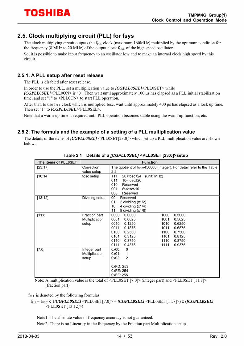
2.5.2. The formula and the example of a setting of a PLL multiplication value The details of the items of [CGPLL0SEL] <PLL0SET[23:0]> which set up a PLL multiplication value are shown below.
Table 2.1 Details of a [CGPLL0SEL] <PLL0SET [23:0]>setup
The items of PLL0SET Function [23:17] Correction
value setup The quotient of fOSC/450000 (integer). For detail refer to the Table 2.2.
[16:14] fosc setup 111: 20<fosc≤24 (unit: MHz) 011: 10<fosc≤20 010: Reserved 001: 6≤fosc≤10 000: Reserved
[13:12] Dividing setup 00: Reserved 01: 2 dividing (x1/2) 10: 4 dividing (x1/4) 11: 8 dividing (x1/8)
[11:8] Fraction part Multiplication setup
0000: 0.0000 0001: 0.0625 0010: 0.1250 0011: 0.1875 0100: 0.2500 0101: 0.3125 0110: 0.3750 0111: 0.4375
1000: 0.5000 1001: 0.5625 1010: 0.6250 1011: 0.6875 1100: 0.7500 1101: 0.8125 1110: 0.8750 1111: 0.9375
[7:0] Integer part Multiplication setup
0x00: 0 0x01: 1 0x02: 2 : 0xFD: 253 0xFE: 254 0xFF: 255
Note: A multiplication value is the total of <PLL0SET [7:0]> (integer part) and <PLL0SET [11:8]> (fraction part).
fPLL is denoted by the following formulas.
fPLL= fOSC x ([CGPLL0SEL] <PLL0SET[7:0]> + [CGPLL0SEL] <PLL0SET [11:8]>) x ([CGPLL0SEL] <PLL0SET [13:12]>)
Note1: The absolute value of frequency accuracy is not guaranteed. Note2: There is no Linearity in the frequency by the Fraction part Multiplication setup.

TMPM4G Group(1)
Clock Control and Operation Mode
2018-04-03 15 / 53 Rev. 2.0
Note3: fPLL ≤ Maximum Operating Frequency
Table 2.2 PLL correction (example) fOSC(MHz) <PLL0SET> [23:17]
(a decimal, an integral value) 8.00 18 10.00 23 12.00 27 16.00 36 20.00 45
The PLL correction value can be calculated below. fosc = 10.0 MHz o'clock, 10.0/0.45 = 22.22 23;
A decimal fraction is rounded up.
The main examples of a setting of [CGPLL0SEL] <PLL0SET [23:0]> are shown below. It multiplies by PLL, and dividing is carried out and the target Clock frequency (fPLL) is generated for input frequency (fOSC).
A dividing value is chosen from 1/2, 1/4, and 1/8. Moreover, set up the frequency after multiplication in the following ranges. 200 MHz ≤ (fOSC x Multiplication value) ≤ 400 MHz
Table 2.3 PLL0SET setting value (example)
fosc(MHz) Multiplication value
Dividing value
fPLL(MHz) <PLL0SET[23:0]>
8.00 40.0000 1/2 160 0x245028 10.00 32.0000 1/2 160 0x2E5020 12.00 26.6250 1/2 159.75 0x36DA1A 16.00 20.0000 1/2 160 0x48D014 20.00 16.0000 1/2 160 0x5AD010
2.5.3. Change of the PLL multiplication value under operation It changes to a setup which sets "0" to [CGPLL0SEL] <PLL0SEL> first, and does not use a PLL multiplication clock during PLL multiplication clock operation when changing a multiplication value. And [CGPLL0SEL] <PLL0ST> =0 is read, after checking having changed to a setup which does not use a multiplication clock, [CGPLL0SEL] <PLL0ON> is set to "0", and PLL is stopped. Then, the multiplication value of [CGPLL0SEL] <PLL0SET> is changed, as reset time of PLL, after about 100 μs progress, [CGPLL0SEL] <PLL0ON> is set as "1", and operation of PLL is started. Then, [CGPLL0SEL] <PLL0SEL> is set as "1" after lock-up time and about 400μs progress. Finally, [CGPLL0SEL]<PLL0ST> are read and it checks having changed.

TMPM4G Group(1)
Clock Control and Operation Mode
2018-04-03 16 / 53 Rev. 2.0
2.5.4. PLL operation start / stop / switching procedure 2.5.4.1. fc setup (PLL stop >>> PLL start)
As an fc setup, the example of switching procedure from the PLL stop state to the PLL operation state is as follows.
<< The example of switching procedure >>
1 [CGSYSCR]<MCKSEL[1:0]> = 01 or 1* Ratios of (High speed system clock vs Middle speed system clock) and (High speed prescaler clock vs High speed system clock) are changed.
2 [CGSYSCR]<MCKSELGST><MCKSELPST> is read Wait until they become the values set at Step 1.
3 [CGPLL0SEL] <PLL0SET> = 0xX A PLL multiplication value setup is chosen. 4 Wait 100 μs or more. Latency time after a multiplication setup 5 [CGPLL0SEL]<PLL0ON> = 1 PLL operation for fsys is carried out to an oscillation. 6 Wait 400 μs or more. PLL output clock stable latency time 7 [CGPLL0SEL]<PLL0SEL> = 1 PLL selection for fsys is carried out to PLL use (fPLL).
8 [CGPLL0SEL]<PLL0ST> is read It waits until the PLL selection status for fsys becomes PLL use (fPLL) (= 1).
Note1: 1 and 2 are executed when the ratio of the system clock should be changed. Note2: 3 to 6 are unnecessary when the state before switching is [CGPLL0SEL] <PLL0ON> = 1.
When changing from the state where the PLL output clock was stable, it can be changed to the PLL operation state by execution of only 7 and 8.
2.5.4.2. fc setup (conduct PLL >>> PLL stop) As an fc setup, the example of switching procedure from the PLL operation state to a PLL stop state is as follows.
<< The example of switching sequence >> 1 [CGPLL0SEL]<PLL0SEL> = 0 Select the PLL for fsys to “PLL is unused (fosc)”.
2 [CGPLL0SEL]<PLL0ST> is read Waits until the status of the PLL for fsys becomes “PLL is unused (fosc) (=0)”.
3 [CGPLL0SEL]<PLL0ON> =0 Sets the PLL operation for fsys to stop.
<< The state before switching >> [CGPLL0SEL]<PLL0ON> = 0 Stops the PLL operation for fsys. [CGPLL0SEL]<PLL0SEL> = 0 Selects the setting of the PLL for fsys to “PLL is unused (fosc)”. [CGPLL0SEL]<PLL0ST> = 0 Selects the status of the PLL for fsys to “PLL is unused (fosc)”.
[CGSYSCR]<MCKSEL> = 00 Ratios of (High speed system clock vs Middle speed system clock) and (High speed prescaler clock vs Middle speed system clock) are 1:1.
<< The state before switching >> [CGPLL0SEL]<PLL0ON> = 1 Sets the PLL for fsys to oscillate. [CGPLL0SEL]<PLL0SEL> = 1 Select the PLL for fsys to “PLL is used (fPLL)”. [CGPLL0SEL]<PLL0ST> = 1 Select the status of the PLL for fsys to “PLL is used (fPLL)”.

TMPM4G Group(1)
Clock Control and Operation Mode
2018-04-03 17 / 53 Rev. 2.0
System clock 2.6.An internal high speed oscillation clock and external high speed oscillation clock (connected oscillator or clock input) can be used as a source of system clock. The system clock consists of “High speed system clock (fsysh)(maximum 160MHz )” for high speed operation and “Middle speed system clock (fsysm)(maximum 80MHz)” which is generated by dividing High speed system clock. Middle speed system clock is used by peripheral function to save power dissipation without degrading CPU performance. The clock domains of the peripheral function can be checked in Table 2.4. High speed system clock can be generated by dividing fc using [CGSYSCR] <GEAR [2:0]> (Clock gear). And Middle speed system clock is generated by dividing the high speed system clock using [CGSYSCR] <MCKSEL[1:0]>. Although a setting can be changed during operation, after register writing before the clock actually changes, a time interval shown in Table 2.5 is required. The completion of the clock change should be checked by [CGSYSCR] <GEARST [2:0]> <MCKSELGST[1:0]>.
Table 2.4 Clock domains of CPU and peripherals Clock domain Block
High speed system clock CPU, Code FLASH, Data FLASH, HDMAC EBIF, SMIF, TSPI(ch0 to 5), CG, INT(IB)
Middle speed system clock
MDMAC, NBDIF, I2C, SIWDT, UART, FUART DAC, TSPI(ch6 to 8), T32A, ADC, Port, PMD DNF, LTTMR, LVD, RLM, ISD, TRM, FLASH(SFR), OFD
Table 2.5 Time interval for changing System clock System clock High speed (fsysh) Middle speed (fsysm)
fsys 16 fc cycles at maximum 16 fc cycles at maximum fsys/2 - 32 fc cycles at maximum fsys/4 - 64 fc cycles at maximum
Note1: The clock gear and the system clock should not be changed while the peripheral function such as the
timer/counter is operating. Note2: An access cannot be done when the system clock is changing between High speed system clock domain
and Middle speed system clock domain.
TMPM4G Group(1)
Clock Control and Operation Mode
2018-04-03 18 / 53 Rev. 2.0
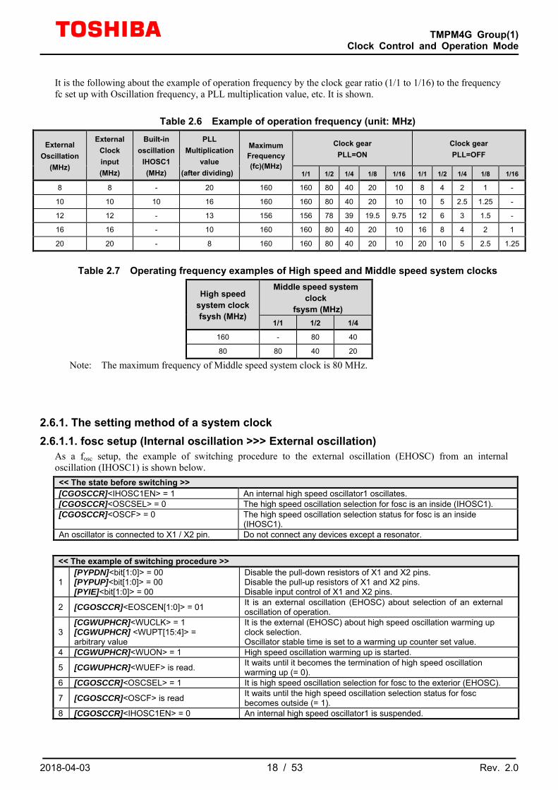
It is the following about the example of operation frequency by the clock gear ratio (1/1 to 1/16) to the frequency fc set up with Oscillation frequency, a PLL multiplication value, etc. It is shown.
Table 2.6 Example of operation frequency (unit: MHz)
External Oscillation
(MHz)
External Clock input (MHz)
Built-in oscillation
IHOSC1 (MHz)
PLL Multiplication
value (after dividing)
Maximum Frequency (fc)(MHz)
Clock gear PLL=ON
Clock gear PLL=OFF
1/1 1/2 1/4 1/8 1/16 1/1 1/2 1/4 1/8 1/16
8 8 - 20 160 160 80 40 20 10 8 4 2 1 -
10 10 10 16 160 160 80 40 20 10 10 5 2.5 1.25 -
12 12 - 13 156 156 78 39 19.5 9.75 12 6 3 1.5 -
16 16 - 10 160 160 80 40 20 10 16 8 4 2 1
20 20 - 8 160 160 80 40 20 10 20 10 5 2.5 1.25
Table 2.7 Operating frequency examples of High speed and Middle speed system clocks
High speed system clock fsysh (MHz)
Middle speed system clock
fsysm (MHz) 1/1 1/2 1/4
160 - 80 40
80 80 40 20
Note: The maximum frequency of Middle speed system clock is 80 MHz.
2.6.1. The setting method of a system clock 2.6.1.1. fosc setup (Internal oscillation >>> External oscillation)
As a fosc setup, the example of switching procedure to the external oscillation (EHOSC) from an internal oscillation (IHOSC1) is shown below.
<< The example of switching procedure >>
1 [PYPDN]<bit[1:0]> = 00 [PYPUP]<bit[1:0]> = 00 [PYIE]<bit[1:0]> = 00
Disable the pull-down resistors of X1 and X2 pins. Disable the pull-up resistors of X1 and X2 pins. Disable input control of X1 and X2 pins.
2 [CGOSCCR]<EOSCEN[1:0]> = 01 It is an external oscillation (EHOSC) about selection of an external oscillation of operation.
3 [CGWUPHCR]<WUCLK> = 1 [CGWUPHCR] <WUPT[15:4]> = arbitrary value
It is the external (EHOSC) about high speed oscillation warming up clock selection. Oscillator stable time is set to a warming up counter set value.
4 [CGWUPHCR]<WUON> = 1 High speed oscillation warming up is started.
5 [CGWUPHCR]<WUEF> is read. It waits until it becomes the termination of high speed oscillation warming up (= 0).
6 [CGOSCCR]<OSCSEL> = 1 It is high speed oscillation selection for fosc to the exterior (EHOSC).
7 [CGOSCCR]<OSCF> is read It waits until the high speed oscillation selection status for fosc becomes outside (= 1).
8 [CGOSCCR]<IHOSC1EN> = 0 An internal high speed oscillator1 is suspended.
<< The state before switching >>
[CGOSCCR]<IHOSC1EN> = 1 An internal high speed oscillator1 oscillates. [CGOSCCR]<OSCSEL> = 0 The high speed oscillation selection for fosc is an inside (IHOSC1). [CGOSCCR]<OSCF> = 0 The high speed oscillation selection status for fosc is an inside
(IHOSC1). An oscillator is connected to X1 / X2 pin. Do not connect any devices except a resonator.
TMPM4G Group(1)
Clock Control and Operation Mode
2018-04-03 19 / 53 Rev. 2.0
2.6.1.2. fosc setup (Internal oscillation >>> External clock input)
As a fosc setup, the example of switching procedure to the external clock input (EHCLKIN) from an internal oscillation 1(IHOSC1) is shown below.
<< The example of switching procedure >>
1 [PYPDN]<bit[1:0]> = 00 [PYPUP]<bit[1:0]> = 00 [PYIE]<bit[0]> = 0
Disable the pull-down resistor of X1 and X2 pins. Disable the pull-up resistors of X1 and X2 pins. Enable the input control of X1/EHCLKIN pin.
2 [CGOSCCR]<EOSCEN[1:0]> = 10 Selection of an external oscillation of operation is carried out to an external clock input (EHCLKIN).
3 [CGOSCCR]<OSCSEL> = 1 It is high speed oscillation selection for fosc to an external clock.
4 [CGOSCCR]<OSCF> is read It waits until the high speed oscillation selection status for fosc becomes outside (= 1).
5 [CGOSCCR]<IHOSC1EN> = 0 An internal high speed oscillator1 is suspended.
2.6.1.3. fosc setup (External oscillation/External clock input >>> Internal oscillation) As a fosc setup, the example of switching procedure to the internal oscillation (IHOSC1) from an external oscillation (EHOSC) Operation State or an external clock input (EHCLKIN) Operation State is shown below.
<< The example of switching procedure >>
1 [CGOSCCR]<IHOSC1EN> = 1 An internal high speed oscillator1 is oscillated.
2 [CGOSCCR]<IHOSC1F> is read It waits until an internal high speed oscillation stable flag becomes oscillation stability (= 1).
3 [CGOSCCR]<OSCSEL> = 0 It is high speed oscillation selection for fosc to an internal clock (IHOSC1).
4 [CGOSCCR]<OSCF> is read It waits until the high speed oscillation selection status for fosc becomes an inside (= 0).
5 [CGOSCCR]<EOSCEN[1:0]> = 00 Set the selection of an external oscillator operation to unused.
<< The state before switching >>
[CGOSCCR]<IHOSC1EN> = 1 An internal high speed oscillator1 oscillates. [CGOSCCR]<OSCSEL> = 0 The high speed oscillation selection for fosc is an inside (IHOSC1).
[CGOSCCR]<OSCF> = 0 The high speed oscillation selection status for fosc is an inside (IHOSC1).
Clock into to EHCLKIN Input in the proper voltage range.
<< The state before switching >>
[CGOSCCR]<EOSCEN[1:0]> = 01 or 10 Selection of an external oscillator of operation is an external oscillator (EHOSC) or external clock input.
[CGOSCCR]<OSCSEL> = 1 The high speed oscillation selection for fosc is the exterior (EHOSC).
[CGOSCCR]<OSCF> = 1 The high speed oscillation selection status for fosc is the exterior (EHOSC).

TMPM4G Group(1)
Clock Control and Operation Mode
2018-04-03 20 / 53 Rev. 2.0
Low speed clock 2.7.
2.7.1. ELOSC Setting (No Operation of External Low Speed Oscillator >>> Operation) An example of setting procedure is shown as follows to use the external low speed oscillator (ELOSC).
<< The example of switching procedure >>
1 [PYPDN]<bit[2:3]> = 00 [PYPUP]<bit[2:3]> = 00 [PYIE]<bit[2]> = 0
The pull-down resistors on XT1/XT2 pins are disabled. The pull-up resistors on XT1/XT2 pins are disabled. Input control of XT1 pin is disabled.
2 [RLMLOSCCR]<DRCOSCL> = 1 The external low speed clock source is set to the external low speed oscillator (ELOSC).
3 [RLMLOSCCR]<XTEN> = 1 The operation of the external low speed oscillator is set.
4 [CGWUPLCR]<WUPTL> = arbitrary value The oscillation stability time should be set to the warming up counter.
5 [CGWUPLCR]<WULON> = 1 The low speed oscillator warming up starts.
6 [CGWUPLCR]<WULEF> is read Wait for the completion (= 0) of the low speed oscillator warming up.
2.7.2. ELCLKIN Setting (No Operation of External Low Speed Oscillator >>> Operation) An example of setting procedure is shown as follows to use the external low speed clock input (ELCLKIN).
<< The example of switching procedure >>
1 [PYPDN]<bit[2:3]> = 00 [PYPUP]<bit[2:3]> = 00 [PYIE]<bit[2]> = 1
The pull-down resistors on XT1/XT2 pins are disabled. The pull-up resistors on XT1/XT2 pins are disabled. Input control of ELCLKIN pin is enable
2 [RLMLOSCCR]<DRCOSCL> = 0 The external low speed clock source is set to the external low speed clock input (ELCLKIN).
3 [RLMLOSCCR]<XTEN> = 1 The operation of the external low speed oscillator is set.
4 [[CGWUPLCR]<WUPTL> = arbitrary value The oscillation stability time should be set to the warming up counter.
5 [CGWUPLCR]<WULON> = 1 The low speed oscillator warming up starts.
6 [CGWUPLCR]<WULEF> is read Wait for the completion (= 0) of the low speed oscillator warming up.
Clock supply setting function 2.8.This MCU has the clock on/off function for the peripheral circuits. To reduce the power consumption, this MCU can stop supplying the clock to the peripheral functions that are not used. Except some peripheral functions, clocks are not supplied after reset. In order to supply the clock of the function to be used, set the bit of relevance of [CGFSYSENA], [CGFSYSMENA], [CGFSYSMENB], [CGSPCLKEN] and [RLMLOSCCR] to “1”. For details, refer to “4 Explanation of a register”.
<< The state before switching >>
[RLMLOSCCR]<XTEN> = 0 The operation state of the external low speed oscillator is selected to “Stop”.
[RLMLOSCCR]<DRCOSCL> = 0 The external input clock (ELCLKIN) is selected as the low speed clock.
<< The state before switching >>
[RLMLOSCCR]<XTEN> = 0 The operation state of the external low speed oscillator is selected to “Stop”.
[RLMLOSCCR]<DRCOSCL> = 0 The external input clock (ELCLKIN) is selected as the low speed clock.
TMPM4G Group(1)
Clock Control and Operation Mode
2018-04-03 21 / 53 Rev. 2.0
Prescaler clock 2.9.Each peripheral function has a prescaler circuit to divide the ΦT0 clock. The ΦT0 clock which is input into the prescaler circuit can be divided by the [CGSYSCR]<PRCK[3:0]> to generate High speed prescaler clock. And Middle speed prescaler clock is generated by dividing High speed prescaler clock using [CGSYSCR]<MCKSEL[1:0]>. For ΦT0 clock after reset, fc is chosen. After register writing before a clock actually changes, a time interval shown in Table 2.8 is required. To confirm the completion of the clock change, check the status of [CGSYSCR] <PRCKST[3:0]> <MCKSELPST[1:0]>.
Table 2.8 Time interval for changing prescaler clocks
Prescaler clock High speed (ΦT0h) Middle speed (ΦT0m) ΦT0 512 fc cycles at maximum 512 fc cycles at maximum ΦT0/2 - 1024 fc cycles at maximum ΦT0/4 - 2048 fc cycles at maximum
Note1: Do not change a prescaler clock during operation of peripheral functions, such as a timer counter. Note2: An access cannot be done when the prescaler clock is changing between High speed system clock domain
and Middle speed system clock domain.

TMPM4G Group(1)
Clock Control and Operation Mode
2018-04-03 22 / 53 Rev. 2.0
3. Operation mode There are NORMAL mode and a Low Power consumption mode (IDLE, STOP1, STOP2) in this product as an Operation mode, and it can reduce power consumption by performing mode changes according to directions for use.
Details of an Operation mode 3.1.
3.1.1. The feature in each mode The feature in NORMAL, Low power consumption modes is as follows.
● NORMAL mode
CPU core and peripheral circuits operate with the high speed oscillation clock. After reset release the system operates in NORMAL mode.
● Low power consumption mode
The feature in Low power consumption modes is as follows.
- IDLE mode It is the mode which CPU stops. The peripheral function should perform operation/stop by the register of each peripheral function, a clock supply setting function, etc
Note: In IDLE mode, the CPU cannot perform the clearance of the watchdog timer, it is careful of it.
- STOP1 mode In this mode, all the internal circuits including the internal oscillator stop. However, when an external low speed oscillator is oscillating and it shifts to STOP1 mode, RTC, CEC, RMC and ISD operate. If it shifts to STOP1 mode when the internal high speed oscillator2 (IHOSC2) is oscillating and LTTMR is selected as a sample clock, CEC and RMC operate. If STOP1 mode is canceled, the internal high speed oscillator1 (IHOSC1) will start oscillation, and the system will return to NORMAL mode. Please disable interrupt which is not used for STOP1 release before shifting to the STOP1 mode.
- STOP2 mode It is the mode which holds a part of functions and cut off internal electrical power source. STOP1 consumption of electric power larger than the STOP2 mode can be held down. If the STOP2 mode is released, power supply will be switched on to the main power domain, a reset sequence will be performed, and it will return to NORMAL mode. As for the Main power domain, it is a function which does not supply a power supply in STOP2 mode.
Before shifting to the STOP2 mode, STOP2 Forbid interruption which is not made into a release factor, Please be sure to set up [RLMSHTDNOP] <PTKEEP> =1 and to hold the state of each port. An Output/Pull-up holds, and input permission hold a state when it sets as a port keeping function. In addition, external interrupt continues an input.
This product will be cut off the power except for the following circuit in STOP2 mode.
▪ External low speed oscillator (ELOSC) ▪ RTC ▪ BackUp RAM

TMPM4G Group(1)
Clock Control and Operation Mode
2018-04-03 23 / 53 Rev. 2.0
▪ Port pin status ▪ LVD ▪ RMC ▪ ISD ▪ CEC ▪ LTTMR ▪ RLM
Regarding a power supply cut off in the Low power consumption mode, for details, refer to the "3.1.4The peripheral function state in a Low Power Consumption mode".
3.1.2. Transition to and Return from Low Power Consumption mode There are IDLE mode, the STOP1 mode, and the STOP2 mode in a Low Power Consumption mode. In order to shift to each Low Power Consumption mode, the IDLE/STOP1/STOP2 mode is chosen by standby control register [CGSTBYCR]<STBY[1:0]>, and a WFI command is executed. When the transition to the low power consumption mode has been done by WFI instruction, the return from the mode can be done by the reset or an interrupt generation. To return by interrupt, it is necessary to set up. Please refer to "interrupt" chapter of the "Exception" of a reference manual for details.
Note1: This product does not support a return by events; therefore, do not make a transition to low-power
consumption mode triggered by WFE (Wait For Event). Note2: This product does not support low power consumption mode by SLEEPDEEP of the Cortex®-M4
processor with FPU core. Do not use the <SLEEPDEEP> bit of the system control register.
3.1.3. Selection of a Low Power Consumption mode Low Power Consumption mode selection is chosen by setup of [CGSTBYCR]<STBY[1:0]>. Following table shows the mode chosen from a setup of <STBY[1:0]>.
Table 3.1 Low Power Consumption mode selection
Mode [CGSTBYCR]<STBY[1:0]>
IDLE 00
STOP1 01
STOP2 10
Note: Do not use the settings other than the above.

TMPM4G Group(1)
Clock Control and Operation Mode
2018-04-03 24 / 53 Rev. 2.0
3.1.4. The peripheral function state in a Low Power Consumption mode The following Table 3.2 shows the Operation State of the peripheral function (block) in each mode. In addition, after reset release it will be in the state where a clock is not supplied except for a part of blocks. If needed, set up [CGFSYSENA],[CGFSYSMENA],[CGFSYSMENB],[CGFCEN],[CGSPCLKEN] and enable clock supply.
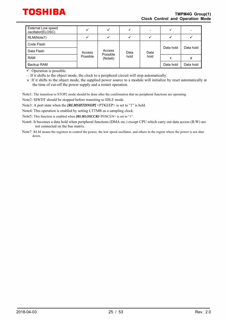
Table 3.2 Block operation status in each Low Power Consumption mode
Block NORMAL IDLE
STOP1 STOP2
ELOSC ELOSC ELOSC ELOSC
On Off On Off
Processor core - - - x x
HDMAC - - x x
MDMAC - - x x
I/O port Pin status (Note3) (Note3)
Register - - x x
EBIF - - x x
ADC - - x x
DAC - - x x
UART - - x x
FUART - - x x
I2C - - x x
TSPI - - x x
SMIF - - x x
A-PMD - - x x
T32A - - x x
LTTMR (Note5) (Note5) (Note5) (Note5) (Note5) (Note5)
TRGSEL - - x x
RTC - x
RMC - (Note4)
CEC - (Note4)
ISD - x
SIWDT (Note2) - - x x
LVD
OFD - - x x
TRM Unavailable - - x x
CG x x
PLL - - x x External High speed ocsillator(EHOSC) - - x x Internal High speed ocsillator 1 (IHOSC1) - - x x
Internal High speed ocsillator 2 (IHOSC2) (Note5) (Note5) (Note5) (Note5) (Note5) (Note5)
TMPM4G Group(1)
Clock Control and Operation Mode
2018-04-03 25 / 53 Rev. 2.0
External Low speed oscillator(ELOSC) - -
RLM(Note7)
Code Flash
Access Possible
Access Possible (Note6)
Data hold
Data hold
Data hold Data hold Data Flash
RAM x x Backup RAM Data hold Data hold
: Operation is possible. - : If it shifts to the object mode, the clock to a peripheral circuit will stop automatically. x : If it shifts to the object mode, the supplied power source to a module will initialize by reset automatically at
the time of cut-off the power supply and a restart operation.
Note1: The transition to STOP2 mode should be done after the confirmation that no peripheral functions are operating. Note2: SIWDT should be stopped before transiting to IDLE mode. Note3: A port state when the [RLMSHTDNOP] <PTKEEP> is set to "1" is held. Note4: This operation is enabled by setting LTTMR as a sampling clock. Note5: This function is enabled when [RLMLOSCCR]<POSCEN> is set to “1”. Note6: It becomes a data hold when peripheral functions (DMA etc.) except CPU which carry out data access (R/W) are
not connected on the bus matrix. Note7: RLM means the registers to control the power, the low speed oscillator, and others in the region where the power is not shut
down.

TMPM4G Group(1)
Clock Control and Operation Mode
2018-04-03 26 / 53 Rev. 2.0
Switch to and return from a Low Power Consumption mode 3.2.
Reset
NORMAL Mode
IDLE Mode (CPU stops)
(Operating peripheral function can be selected)
After reset the high speed oscillator1(IHOSC1) oscillates.
Interrupt
STOP1 Mode (CPU stops except some
peripheral functions)
Interrupt
Instruction
Instruction (Note1)
(Note2)
STOP2 Mode(CPU stops with shutdown internal
power supply except some peripheral functions)
Interrupt
Instruction
(Note2)
Reset(Shutdown internal power
supply block)
Interrupt
Figure 3.1 Change state
Note1: Warm-up is required at returning. A warm-up time must be set in the previous mode (NORMAL mode)
before entering to STOP1 mode. Note2: When the MCU returns from STOP2 mode, the MCU branches to the interrupt service routine triggered by
reset. When the MCU returns from STOP1 mode, the MCU branches to the interrupt service routine triggered by interrupt events.
3.2.1. IDLE mode transition flow Set up the following procedure at switching to IDLE mode. Because IDLE mode is released by an interrupt, set the interrupt before switching to IDLE mode. For the interrupts that can be used to release the IDLE mode, refer to "3.3.1The release source of a Low Power Consumption mode". Disable interrupts not used for release and interrupts that can not be used.
Switching procedure (from Normal mode)
1 [SIWDxEN]<WDTE>=0 Disable SIWDT. 2 [SIWDxCR]<WDCR[7:0]>=0xB1 Disable SIWDT. 3 [FCSR0]<RDYBSY> is read It waits until Flash will be in a Ready state (= 1). 4 [CGSTBYCR]<STBY[1:0]>=00 Low Power Consumption mode selection is set to IDLE. 5 [CGSTBYCR]<STBY[1:0]> is read Check the 4th line register writing (= 00). 6 WFI command execution Switch to IDLE

TMPM4G Group(1)
Clock Control and Operation Mode
2018-04-03 27 / 53 Rev. 2.0
3.2.2. STOP1 mode transition flow Set up the following procedure at switching to STOP1. Because STOP1 mode is released by an interrupt, set the interrupt before switching to STOP1 mode. For the interrupts that can be used to release the STOP1 mode, refer to "3.3.1The release source of a Low Power Consumption mode". Disable interrupts not used for release and interrupts that can not be used.
I Switching procedure (from Normal mode)
1 [SIWDxEN]<WDTE>=0 Disable SIWDT. 2 [SIWDxCR]<WDCR[7:0]>=0xB1 Disable SIWDT. 3 [FCSR0]<RDYBSY> is read It waits until Flash will be in a Ready state (=1).
4 [CGWUPHCR]<WUEF> is read It waits until it becomes the termination of high speed oscillation warming up (=0).
5 [CGWUPHCR]<WUCLK>=0 High speed oscillation warming up clock selection is made into an
inside (IHOSC1). [CGWUPHCR]<WUPT[15:4]>= “arbitrary value”
A high speed oscillation warming up counter set value is set as time required for STOP1 restart operation.
6 [CGSTBYCR]<STBY[1:0]>=01 Low Power Consumption mode selection is set to STOP1. 7 [CGPLL0SEL]<PLL0SEL>=0 Set PLL of fsys to fosc (= PLL no USE) 8 [CGPLL0SEL]<PLL0ST> is read Wait for PLL status of fsys until off state (fosc = 0). 9 [CGPLL0SEL]<PLL0ON>=0 Stop PLL for fsys
10 [CGOSCCR]<IHOSC1EN>=1 Enable the internal high speed oscillator.
11 [CGOSCCR]<OSCSEL>=0 High speed oscillation selection for fosc is made into an inside (IHOSC1).
12 [CGOSCCR]<OSCF> is read It waits until the high speed oscillation selection status for fosc becomes an inside (IHOSC1) (=0).
13 [CGOSCCR]<EOSCEN[1:0]>=00 Selection of an external oscillation of operation is unused.
14 [RLMLOSCCR]<POSCEN>=0 or 1 Setting for the internal high speed oscillator 2 (IHOSC2). 1: LTTMR operates in STOP1 mode. 0: Others.
15 [CGOSCCR]<EOSCEN[1:0]> is read The register writing of above 13th is checked (=00).
16 [RLMLOSCCR]<POSCF> is read It wait until the internal high speed oscillation stable flag become zero.
17 WFI command execution Switch to STOP1.

TMPM4G Group(1)
Clock Control and Operation Mode
2018-04-03 28 / 53 Rev. 2.0
3.2.3. STOP2 mode transition flow Set up the following procedure at switching to STOP2. Because STOP2 mode is released by an interrupt, set the interrupt before switching to STOP2 mode. For the interrupts that can be used to release the STOP2 mode, refer to "3.3.1The release source of a Low Power Consumption mode". Disable interrupts not used for release and interrupts that can not be used.
Switching procedure
1 [SIWDxEN]<WDTE>=0 Disable SIWDT. 2 [SIWDxCR]<WDCR[7:0]>=0xB1 Disable SIWDT. 3 [FCSR0]<RDYBSY> is read It waits until Flash will be in a Ready state (= 1). 4 [RLMSHTDNOP]<PTKEEP>=1 IO control signal is made to hold. 5 [CGSTBYCR]<STBY[1:0]>=10 Low Power Consumption mode selection is set to STOP2. 6 [CGPLL0SEL]<PLL0SEL>=0 the PLL selection for fsys is set to PLL unused (fosc) 7 [CGPLL0SEL]<PLL0ST> is read It waits until the PLL selection status for fsys is PLL un-using it. (= 0). 8 [CGPLL0SEL]<PLL0ON>=0 Stop PLL for fsys. 9 [CGOSCCR]<IHOSC1EN>=1 Enable the internal high speed oscillator.
10 [CGOSCCR]<OSCSEL>=0 High speed oscillation selection for fosc is set to the inside (IHOSC1).
11 [CGOSCCR]<OSCF> is read It waits until the high speed oscillation selection status for fosc becomes zero (IHOSC1) (=0).
12 [CGOSCCR]<EOSCEN[1:0]>=00 Selection of an external oscillation of operation is set to stop.
13 [RLMLOSCCR]<POSCEN>=0 or 1 Setting for the internal high speed oscillator 2 (IHOSC2). 1: LTTMR operates in STOP1 mode. 0: Others.
14 [CGOSCCR]<EOSCEN[1:0]> is read The register writing of 12 is checked (=00). 15 [RLMLOSCCR]<POSCF> is read It wait until the internal oscillation stable flag become zero.
16 [RLMRSTFLG0]<STOP2RSTF>=0 [RLMRSTFLG0]< PINRSTF>=0 A STOP2 reset flag / reset pin flag is cleared (Note1).
17 WFI command execution Switch to STOP2. 18 Jump instruction Return to 17.
Note: Refer to the "Exception" of a reference manual for a reset flag register [RLMRSTFLG0].

TMPM4G Group(1)
Clock Control and Operation Mode
2018-04-03 29 / 53 Rev. 2.0
Return from a Low Power Consumption mode 3.3.
3.3.1. The release source of a Low Power Consumption mode Interrupt, Non-Maskable Interrupt, and reset can perform release from a Low Power Consumption mode. The standby release source which can be used is decided by a Low Power Consumption mode. It shows the following table about details.
Table 3.3 Release source list
Low Power Consumption mode IDLE STOP1 STOP2
Release Source
Interrupt
INT00 to INT15 (Note) INTRTC INTCECRX,INTCECTX INTISDx INTRMCx INTLTTMR INTHDMAxTC, INTHDMAxERR x x INTMDMAxTC, INTMDMAxBERR, INTMDMAxDERR x x INT32Ax_A_CT, INT32Ax_B_Cx_CPC x x INTADCPA,INTADCPB,INTADTRG x x INTEMGx, INTOVVx, INTPWMx x x INTTxRX,INTTxTX,INTTxERR x x INTSMIx x x INTUTxRX,INTUTxTX,INTUTxERR x x INTUARTx x x INTI2C, INTI2CAL, INTI2CBF,INTI2CNACK x x INTADxCP0, INTADxCP1, INTADxSGL, INTADxCNT INTADxHP x x
INTFLCRDY0, INTFLCRDY1, INTFLDRDY x x SysTick interrupt x x Non-Maskable Interrupt (INTWDT) x x x Non-Maskable Interrupt (INTLVD) Reset (SIWDT) x x x Reset (LVD) Reset (OFD) x x Reset (RESET_N pin)
: After release, the interrupt procedure will start. x: It cannot be used for release. Note: INT00 to INT15(External Interrupt 00 to 15) can select one of falling edge, rising edge and level. For
details, please refer to “Exception” of reference manual.

TMPM4G Group(1)
Clock Control and Operation Mode
2018-04-03 30 / 53 Rev. 2.0
● Released by an interrupt request When interrupt cancels a Low Power Consumption mode, it is necessary to prepare so that interrupt may be detected by CPU. The interrupt used for release in STOP1 and the STOP2 mode needs to interrupt by INTIF other than a setup of CPU, and needs to set up detection.
● Released by Non-Maskable Interrupt (NMI)
The LVD interrupt (INTLVD) can perform release from the Low Power Consumption modes.
● Released by reset The reset can perform release from all the Low Power Consumption modes. When released by reset, all the registers will be initialized in NORMAL mode after release.
● Released by SysTick interrupt
SysTick interrupt is available only in IDLE mode. Refer to "Interrupt" chapter of a reference manual of "Exception" about the details of interrupt.
3.3.2. Warming up at the release of Low Power Consumption mode Warming up may be required because of stability of an internal oscillator at the time of mode transition. When the transition from STOP1 mode to NORMAL mode is done, the internal oscillation is selected automatically and the warming up counter starts up.The Output of a system clock is started after warming up time progress.
For this reason, before executing the command which move to the STOP1 mode, set up warming up time by [CGWUPHCR]<WUPT[15:4]>. For the setting method, refer to the "2.4.1The warming up counter for a high speed oscillation".
The following table shows the existence of a warming up setup at the time of each Operation mode transition.
Table 3.4 Warming up Operation mode transition Warming up setup
NORMAL >>> IDLE Not required. NORMAL >>> STOP1 Not required. NORMAL >>> STOP2 Not required. IDLE >>> NORMAL Not required. STOP1 >>> NORMAL Required. STOP2 >>> RESET >>> NORMAL Not required.

TMPM4G Group(1)
Clock Control and Operation Mode
2018-04-03 31 / 53 Rev. 2.0
3.3.3. Restart operation from STOP2 mode The restart operation flow from STOP2 mode release factor interrupt generating is as follows.
STOP2 release interrupt Reset by RESET_N pin
Figure 3.2 STOP2 mode restart operation flow
Note1: When STOP2 released by a reset pin, as for a reset flag, both "STOP2 reset flag" and "reset pin flag" are materialized.
Note2: Register reset area in STOP2 Release differs by the case of interrupt and a reset pin. Refer to the reference manual "Power Supply and Reset Operation" for the details of each reset area.
Release factor generating
Check reset flag (Note1) [RLMRSTFLGx]=xx (it is checked by which factor reset has occurred)
Release the port state hold function • Initial setting at the return of STOP2 and
re-setup of the port registers. • [RLMSHTDNOP]<PTKEEP> = 0 (possible to
control a port)
Return to the NORMAL mode with all register initialized.
Interrupt procedure •Setting for interrupt enable register, interrupt priority register. • Jump to the interrupt procedure and check the STOP2 return factor
Re-setup of register (Note2) • Resetting each function register with register initialization
Re-setup of register (Note2) • Resetting each function with register
initialization

TMPM4G Group(1)
Clock Control and Operation Mode
2018-04-03 32 / 53 Rev. 2.0
Clock operation by mode transition 3.4.The clock operation in case of mode transition is shown below.
3.4.1. NORMAL >>> IDLE >>> NORMAL Operation mode transition CPU stops at IDLE mode. The clock supply to a peripheral function holds a setting state. Please perform operation/stop by the register of each peripheral function, a clock supply setting function, etc. if needed. Execution of Warming up operation is not performed at the time of the restart operation in NORMAL mode from IDLE state. After the command (WFI) execution which switch to IDLE mode, a program counter will show the next point and will be in a CPU idle state. With a release source, it becomes a CPU reboot and, in the case of an enable interrupt state, the shift to next point by transition command (WFI) will be done, after the interrupt processing by release source.
3.4.2. NORMAL >>> STOP1 >>> NORMAL Operation mode transition When returning to NORMAL mode from the STOP1 mode, warming up is started automatically. Please set warming up time (8 μs at minimum) to [CGWUPHCR] <WUPT[15:4]> before moving to the STOP1 mode.
Warm up
fosc
Mode
fsys(system clock)
NORMAL STOP1 NORMAL
WFI intsruction execution/Sleep on exit
Generate Release factor
System clock stops Start IHOSC1Start Warm up
Warming up time
Warm up endsSystem clock operation
Figure 3.3 NORMAL >>> STOP1 >>> NORMAL Operation mode transition
TMPM4G Group(1)
Clock Control and Operation Mode
2018-04-03 33 / 53 Rev. 2.0
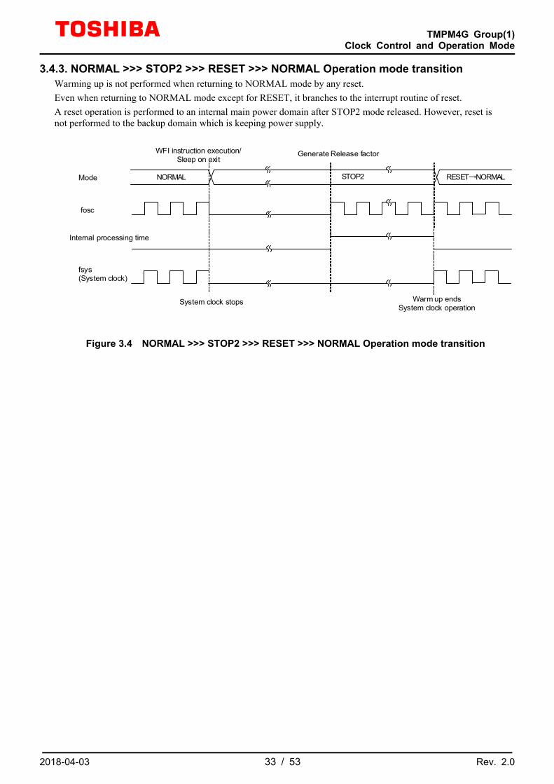
3.4.3. NORMAL >>> STOP2 >>> RESET >>> NORMAL Operation mode transition Warming up is not performed when returning to NORMAL mode by any reset. Even when returning to NORMAL mode except for RESET, it branches to the interrupt routine of reset. A reset operation is performed to an internal main power domain after STOP2 mode released. However, reset is not performed to the backup domain which is keeping power supply.
Internal processing time
fosc
Mode
fsys(System clock)
NORMAL STOP2 RESET→NORMAL
WFI instruction execution/Sleep on exit
Generate Release factor
System clock stops Warm up endsSystem clock operation
Figure 3.4 NORMAL >>> STOP2 >>> RESET >>> NORMAL Operation mode transition

TMPM4G Group(1)
Clock Control and Operation Mode
2018-04-03 34 / 53 Rev. 2.0
4. Explanation of a register
Register list 4.1.The register related to CG and its address information are shown below.
Peripheral function Channel/Unit Base address
Clock Control and Operation Mode CG - 0x40083000
Low speed oscillation/ power control RLM - 0x4003E400
Clock Control and Operatio Mode Register name Address (Base+)
CG write protection register [CGPROTECT] 0x0000
Oscillation control register [CGOSCCR] 0x0004
System clock control register [CGSYSCR] 0x0008
Standby control register [CGSTBYCR] 0x000C
PLL selection register for fsys [CGPLL0SEL] 0x0020
High speed oscillation warming up register [CGWUPHCR] 0x0030
Low speed oscillation warming up register [CGWUPLCR] 0x0034
Middle speed clock supply and stop register A for fsys [CGFSYSMENA] 0x0048
Middle speed clock supply and stop register B for fsys [CGFSYSMENB] 0x004C
High speed clock supply and stop register A for fsys [CGFSYSENA] 0x0050
Clock supply and stop register for fc [CGFCEN] 0x0058
Clock supply for ADC and Trace Register [CGSPCLKEN] 0x005C
Function extension register 2 [CGEXTEND2] 0x0068
Low speed oscillation/power shutdown control (Note1,Note2) Register name Address (Base+)
Low speed oscillation and Internal High speed oscillation 2 clock control register [RLMLOSCCR] 0x0000
Power supply cut off control register [RLMSHTDNOP] 0x0001
RLM write protection register [RLMPROTECT] 0x000F
Note1: Byte accessible registers. Bit band access cannot be performed. Note2: When you rewrite, read the register and check rewriting.
In addition, when the reserved area is written, the initial value should be set.

TMPM4G Group(1)
Clock Control and Operation Mode
2018-04-03 35 / 53 Rev. 2.0
Detail of Register 4.2.
4.2.1. [CGPROTECT] (CG write protection register)
Bit Bit Symbol After reset Type Function
31:8 - 0 R Read as “0”.
7:0 PROTECT[7:0] 0xC1 R/W
Control write-protection for the CG register (all registers included except this register) 0xC1: CG Registers are write-enabled. Other than 0xC1: Sets write protection (Protect enable)
4.2.2. [CGOSCCR] (Oscillation control register)
Bit Bit Symbol After reset Type Function
31:17 - 0 R Read as "0".
16 IHOSC1F 1 R Indicates the stability flag of internal oscillation 1 for IHOSC1 0: Stopping or being in warm up 1: Stable oscillation
15:13 - 0 R Read as "0".
12 - 0 R/W Write as "0".
11:10 - 0 R Read as "0".
9 OSCF 0 R Indicates high speed oscillator for fosc selection status. 0: Internal high speed oscillator 1 (IHOSC1) 1: External high speed oscillator (EHOSC)
8 OSCSEL 0 R/W Selects a high speed oscillation for fosc. (Note1) 0: Internal high speed oscillator 1 (IHOSC1) 1: External high speed oscillator (EHOSC)
7:4 - 0 R Read as "0".
3 - 0 R/W Write as "0".
2:1 EOSCEN[1:0] 00 R/W
Selects the operation of the external high speed oscillator. (EHOSC) (Note2) 00: External oscillator is not used 01: Uses the external high speed oscillator (EHOSC) 10: Uses the external clock (EHCLKIN) 11: Reserved
0 IHOSC1EN 1 R/W Internal high speed oscillator 1 (IHOSC1) 0: Stop 1: Oscillation
Note1: When the setting is modified, confirm whether the written value has been reflected to the [CGOSCCR] <OSCF> bit before executing the next operation.
Note2: When an external high speed clock (oscillator connection) is used, set “01” to this bit.

TMPM4G Group(1)
Clock Control and Operation Mode
2018-04-03 36 / 53 Rev. 2.0
4.2.3. [CGSYSCR] (System clock control register)
Bit Bit Symbol After reset Type Function
31:30 MCKSELPST[1:0] 00 R
Middle speed prescaler clock (ΦT0) selection status 00: <PRCK[3:0]> setting value (no division) 01: <PRCK[3:0]> setting value is divided by 2 1*: <PRCK[3:0]> setting value is divided by 4
29:28 - 0 R Read as "0".
27:24 PRCKST[3:0] 0000 R
High speed prescaler clock (ΦT0) selection status 0000: fc 0100: fc/16 1000: fc/256 0001: fc/2 0101: fc/32 1001: fc/512 0010: fc/4 0110: fc/64 1010 to 1111: Reserved 0011: fc/8 0111: fc/128
23:22 MCKSELGST[1:0] 00 R
Middle speed system clock (fsys) selection status 00: <GEAR[2:0]> setting value (no division) 01: <GEAR[2:0]> setting value is divided by 2 1*: <GEAR[2:0]> setting value is divided by 4
21:19 - 0 R Read as "0".
18:16 GEARST[2:0] 000 R
High speed system clock (fsys) gear selection status 000: fc 100: fc/16 001: fc/2 101 - 111: Reserved 010: fc/4 011: fc/8
15:12 - 0 R Read as "0".
11:8 PRCK[3:0] 0000 R/W
High speed prescaler clock (ΦT0) selection 0000: fc 0100: fc/16 1000: fc/256 0001: fc/2 0101: fc/32 1001: fc/512 0010: fc/4 0110: fc/64 1010 - 1111: Reserved 0011: fc/8 0111: fc/128 Selects a prescaler clock for the peripheral functions.
7:6 MCKSEL[1:0] 00 R/W
Middle speed system clock (fsys) and Middle speed prescaler clock (ΦT0) selection 00: <GEAR[2:0]>,<PRCK[3:0]> setting values (no division) 01: <GEAR[2:0]>,<PRCK[3:0]> setting values are divided by 2. 1*: <GEAR[2:0]>,<PRCK[3:0]> setting values are divided by 4. Maximum operating frequency of middle speed system clock is 80MHz.
5:3 - 0 R Read as "0".
2:0 GEAR[2:0] 000 R/W
High speed system clock (fsys) gear selection 000: fc 100: fc/16 001: fc/2 101 to 111: Reserved 010: fc/4 011: fc/8

TMPM4G Group(1)
Clock Control and Operation Mode
2018-04-03 37 / 53 Rev. 2.0
4.2.4. [CGSTBYCR] (Standby control register)
Bit Bit Symbol After reset Type Function
31:2 - 0 R Read as "0".
1:0 STBY[1:0] 00 R/W
Selects a low power consumption mode. 00: IDLE 01: STOP1 10: STOP2 11: Reserved
4.2.5. [CGPLL0SEL] (PLL selection register for fsys)
Bit Bit Symbol After reset Type Function
31:8 PLL0SET[23:0] 0x000000 R/W
PLL multiplication setup About a multiplication setup, refer to the “2.5.2The formula and the example of a setting of a PLL multiplication value”.
7:3 - 0 R Read as "0".
2 PLL0ST 0 R Indicates PLL for fsys selection status. 0: fosc 1: fPLL
1 PLL0SEL 0 R/W Indicates Clock selection for fsys 0: fosc 1: fPLL
0 PLL0ON 0 R/W Indicates PLL operation for fsys 0: Stop 1: Oscillation

TMPM4G Group(1)
Clock Control and Operation Mode
2018-04-03 38 / 53 Rev. 2.0
4.2.6. [CGWUPHCR] (High speed oscillation warming up register)
Bit Bit Symbol After reset Type Function
31:20 WUPT[15:4] 0x800 R/W
Sets the upper 12 bits of the 16 bits of calculation values of the warm-up timer. About a setup of a warming up timer, refer to the “2.4.1The warming up counter for a high speed oscillation”.
19:16 WUPT[3:0] 0x0 R Sets the lower 4 bits of the 16 bits of calculation values of the warm up timer. It is fixed to “0x0”.
15:9 - 0 R Read as "0".
8 WUCLK 0 R/W Warming up clock selection (Note1) 0: Internal high speed oscillator 1 (IHOSC1) 1: External high speed oscillator (EHOSC)
7:2 - 0 R Read as "0".
1 WUEF 0 R Indicates status of the Warming up timer.(Note2) 0: The end of Warming up 1: In warming up operation
0 WUON 0 W Control the Warming up timer. 0: don't care 1: Warming up operation start.
Note1: Use the internal oscillator for warm-up when the MCU returns from STOP1 mode. Do not use an external oscillator when the MCU returns from STOP1 mode.
Note2: Do not modify the registers during the warm-up (<WUEF>=1). Set the registers when <WUEF>=0.

TMPM4G Group(1)
Clock Control and Operation Mode
2018-04-03 39 / 53 Rev. 2.0
4.2.7. [CGWUPLCR] (Low speed oscillation warming up register)
Bit Bit Symbol After reset Type Function
31:27 - 0 R Read as "0".
26:12 WUPTL[18:4] 0x4000 R/W
Sets the upper 15 bits of 19 bits of calculation values of the warm-up timer. About a setup of a warming up timer, refer to the “2.4.2The warming up counter for a low speed oscillation“.
11:8 WUPTL[3:0] 0x0 R Sets the lower 4 bits of the 19 bits of calculation values of the warm-up timer. It is fixed to “0x0”.
7:2 - 0 R Read as "0".
1 WULEF 0 R Indicates a status of the Warming up timer (Note) 0: The end of Warming up 1: In warming up operation
0 WULON 0 W Control the Warming up timer control 0: Don't care. 1: Warming up operation start.
Note: Do not modify the registers during the warm-up (<WULEF>=1). Set the registers when <WULEF>=0.

TMPM4G Group(1)
Clock Control and Operation Mode
2018-04-03 40 / 53 Rev. 2.0
4.2.8. [CGFSYSMENA] (Middle speed clock supply and stop register A for fsys)
Bit Bit Symbol After reset Type Function
31 IPMENA31 0 R/W Clock enable of I2C ch2 0: Clock stop 1: Clock supply
30 IPMENA30 0 R/W Clock enable of I2C ch1 0: Clock stop 1: Clock supply
29 IPMENA29 0 R/W Clock enable of I2C ch0 0: Clock stop 1: Clock supply
28 IPMENA28 0 R/W Clock enable of UART ch5 0: Clock stop 1: Clock supply
27 IPMENA27 0 R/W Clock enable of UART ch4 0: Clock stop 1: Clock supply
26 IPMENA26 0 R/W Clock enable of UART ch3 0: Clock stop 1: Clock supply
25 IPMENA25 0 R/W Clock enable of UART ch2 0: Clock stop 1: Clock supply
24 IPMENA24 0 R/W Clock enable of UART ch1 0: Clock stop 1: Clock supply
23 IPMENA23 1 R/W Clock enable of UART ch0 0: Clock stop 1: Clock supply
22 IPMENA22 0 R/W Clock enable of TSPI ch8 0: Clock stop 1: Clock supply
21 IPMENA21 0 R/W Clock enable of TSPI ch7 0: Clock stop 1: Clock supply
20 IPMENA20 0 R/W Clock enable of TSPI ch6 0: Clock stop 1: Clock supply
19 IPMENA19 0 R/W Clock enable of T32A ch13 0: Clock stop 1: Clock supply
18 IPMENA18 0 R/W Clock enable of T32A ch12 0: Clock stop 1: Clock supply
17 IPMENA17 0 R/W Clock enable of T32A ch11 0: Clock stop 1: Clock supply
16 IPMENA16 0 R/W Clock enable of T32A ch10 0: Clock stop 1: Clock supply
15 IPMENA15 0 R/W Clock enable of T32A ch09 0: Clock stop 1: Clock supply
14 IPMENA14 0 R/W Clock enable of T32A ch08 0: Clock stop 1: Clock supply
13 IPMENA13 0 R/W Clock enable of T32A ch07 0: Clock stop 1: Clock supply
12 IPMENA12 0 R/W Clock enable of T32A ch06 0: Clock stop 1: Clock supply
11 IPMENA11 0 R/W Clock enable of T32A ch05 0: Clock stop 1: Clock supply

TMPM4G Group(1)
Clock Control and Operation Mode
2018-04-03 41 / 53 Rev. 2.0
10 IPMENA10 0 R/W Clock enable of T32A ch04 0: Clock stop 1: Clock supply
9 IPMENA09 0 R/W Clock enable of T32A ch03 0: Clock stop 1: Clock supply
8 IPMENA08 0 R/W Clock enable of T32A ch02 0: Clock stop 1: Clock supply
7 IPMENA07 0 R/W Clock enable of T32A ch01 0: Clock stop 1: Clock supply
6 IPMENA06 1 R/W Clock enable of T32A ch00 0: Clock stop 1: Clock supply
5 IPMENA05 0 R/W Clock enable of DAC ch1 0: Clock stop 1: Clock supply
4 IPMENA04 0 R/W Clock enable of DAC ch0 0: Clock stop 1: Clock supply
3 IPMENA03 0 R/W Clock enable of ADC UnitA 0: Clock stop 1: Clock supply
2 IPMENA02 0 R/W Clock enable of FUART ch1 0: Clock stop 1: Clock supply
1 IPMENA01 0 R/W Clock enable of FUART ch0 0: Clock stop 1: Clock supply
0 IPMENA00 0 R/W Clock enable of MDMAC UnitA 0: Clock stop 1: Clock supply
Note1: Even if the initial value of the register is set to stop of the clock, the clock is supplied during the reset. Note2: Write “0” for bit of function that does not exist in TMPM4G8,TMPM4G7 and TMPM4G6.

TMPM4G Group(1)
Clock Control and Operation Mode
2018-04-03 42 / 53 Rev. 2.0
4.2.9. [CGFSYSMENB] (Middle speed clock supply and stop register B for fsys)
Bit Bit Symbol After reset Type Function
31 IPMENB31 1 R/W Clock enable of SIWDT 0: Clock stop 1: Clock supply
30 IPMENB30 1 R/W Clock enable of NBDIF 0: Clock stop 1: Clock supply
29 IPMENB29 1 R/W Write as “1”
28 IPMENB28 0 R/W Clock enable of TRGSEL 0: Clock stop 1: Clock supply
27:25 - 0 R Read as “0”
24 IPMENB24 0 R/W Clock enable of A-PMD 0: Clock stop 1: Clock supply
23 IPMENB23 0 R/W Clock enable of OFD 0: Clock stop 1: Clock supply
22 IPMENB22 0 R/W Clock enable of TRM 0: Clock stop 1: Clock supply
21 IPMENB21 0 R/W Clock enable of PORT Y 0: Clock stop 1: Clock supply
20 IPMENB20 0 R/W Clock enable of PORT W 0: Clock stop 1: Clock supply
19 IPMENB19 0 R/W Clock enable of PORT V 0: Clock stop 1: Clock supply
18 IPMENB18 0 R/W Clock enable of PORT U 0: Clock stop 1: Clock supply
17 IPMENB17 0 R/W Clock enable of PORT T 0: Clock stop 1: Clock supply
16 IPMENB16 0 R/W Clock enable of PORT R 0: Clock stop 1: Clock supply
15 IPMENB15 0 R/W Clock enable of PORT P 0: Clock stop 1: Clock supply
14 IPMENB14 0 R/W Clock enable of PORT N 0: Clock stop 1: Clock supply
13 IPMENB13 0 R/W Clock enable of PORT M 0: Clock stop 1: Clock supply
12 IPMENB12 0 R/W Clock enable of PORT L 0: Clock stop 1: Clock supply
11 IPMENB11 0 R/W Clock enable of PORT K 0: Clock stop 1: Clock supply
10 IPMENB10 0 R/W Clock enable of PORT J 0: Clock stop 1: Clock supply
9 IPMENB09 1 R/W Clock enable of PORT H 0: Clock stop 1: Clock supply
8 IPMENB08 0 R/W Clock enable of PORT G 0: Clock stop 1: Clock supply

TMPM4G Group(1)
Clock Control and Operation Mode
2018-04-03 43 / 53 Rev. 2.0
7 IPMENB07 0 R/W Clock enable of PORT F 0: Clock stop 1: Clock supply
6 IPMENB06 0 R/W Clock enable of PORT E 0: Clock stop 1: Clock supply
5 IPMENB05 0 R/W Clock enable of PORT D 0: Clock stop 1: Clock supply
4 IPMENB04 0 R/W Clock enable of PORT C 0: Clock stop 1: Clock supply
3 IPMENB03 0 R/W Clock enable of PORT B 0: Clock stop 1: Clock supply
2 IPMENB02 0 R/W Clock enable of PORT A 0: Clock stop 1: Clock supply
1 IPMENB01 0 R/W Clock enable of I2C ch4 0: Clock stop 1: Clock supply
0 IPMENB00 0 R/W Clock enable of I2C ch3 0: Clock stop 1: Clock supply
Note1: Even if the initial value of the register is set to stop of the clock, the clock is supplied during the reset. Note2: Write “0” for bit of function that does not exist in TMPM4G8,TMPM4G7 and TMPM4G6.

TMPM4G Group(1)
Clock Control and Operation Mode
2018-04-03 44 / 53 Rev. 2.0
4.2.10. [CGFSYSENA] (High speed clock supply and stop register A for fsys)
Bit Bit Symbol After reset Type Function
31:13 - 0 R Read as “0”
12 IPENA12 0 R/W
Write as “0” 11 IPENA11 0 R/W
10 IPENA10 0 R/W
9 IPENA09 0 R/W Clock enable of TSPI ch5 0: Clock stop 1: Clock supply
8 IPENA08 0 R/W Clock enable of TSPI ch4 0: Clock stop 1: Clock supply
7 IPENA07 0 R/W Clock enable of TSPI ch3 0: Clock stop 1: Clock supply
6 IPENA06 0 R/W Clock enable of TSPI ch2 0: Clock stop 1: Clock supply
5 IPENA05 0 R/W Clock enable of TSPI ch1 0: Clock stop 1: Clock supply
4 IPENA04 0 R/W Clock enable of TSPI ch0 0: Clock stop 1: Clock supply
3 IPENA03 0 R/W Clock enable of EBIF 0: Clock stop 1: Clock supply
2 IPENA02 0 R/W Clock enable of SMIF ch0 0: Clock stop 1: Clock supply
1 IPENA01 0 R/W Clock enable of HDMAC UnitB 0: Clock stop 1: Clock supply
0 IPENA00 0 R/W Clock enable of HDMAC UnitA 0: Clock stop 1: Clock supply
Note1: Even if the initial value of the register is set to stop of the clock, the clock is supplied during the reset. Note2: Write “0” for bit of function that does not exist in TMPM4G8,TMPM4G7 and TMPM4G6.

TMPM4G Group(1)
Clock Control and Operation Mode
2018-04-03 45 / 53 Rev. 2.0
4.2.11. [CGFCEN] (Clock supply and stop register for fc)
Bit Bit Symbol After reset Type Function
31:28 - 0 R Read as “0”
27 FCIPEN27 0 R/W Clock enable of DNF UnitB 0: Clock stop 1: Clock supply
26 FCIPEN26 0 R/W Clock enable of DNF UnitA 0: Clock stop 1: Clock supply
25:24 - 0 R Read as “0”
23 FCIPEN23 0 R/W Clock enable of OFD (Note1) 0: Clock stop 1: Clock supply
22:0 - 0 R Read as “0”
Note1: When use the monitor clock of fc,[CGFSYSMENB]<IPMENB23> and [CGFCEN]<FCIPEN23> should be enabled.
Note2: Even if the initial value of the register is set to stop of the clock, the clock is supplied during the reset. Note3: Write “0” for bit of function that does not exist in TMPM4G8,TMPM4G7 and TMPM4G6.
4.2.12. [CGSPCLKEN] (Clock supply for ADC and Trace Register)
Bit Bit Symbol After reset Type Function
31:17 - 0 R Read as "0".
16 ADCKEN 0 R/W Enable the clock for ADC. 0: Clock stop 1: Clock supply
15:1 - 0 R Read as "0".
0 TRCKEN 0 R/W Enable the Clock for the Trace function of Debug circuit (ETM). 0: Clock stop 1: Clock supply

TMPM4G Group(1)
Clock Control and Operation Mode
2018-04-03 46 / 53 Rev. 2.0
4.2.13. [CGEXTEND2] (Function extension register 2)
Bit Bit Symbol After reset Type Function
31:3 - 0 R Read as "0".
2 RSV22 0 R/W
MDMAC software reset It is generated with the continuous writes of “0” >>> “1” >>> “0”. When this bit is written continuously to “0” >>> “1” >>> ”0”, MDMAC software reset is generated. After “1” is set, 4 cycles of Middle speed system clock (fsysm) or more should elapse before “0” is set.
1 RSV21 0 R/W
MDMAC bus error clear (Note) It is generated with the continuous writes of “0” >>> “1” >>> “0”. MDMAC bus error is cleared by the sequential writes of “0” >>> “1” >>> “0” to this bit.After “1” is set, 4 cycles of Middle speed system clock (fsysm) or more should elapse before “0” is set.
0 RSV20 0 R/W
MDMAC descriptor error clear (Note) It is generated with the continuous writes of “0” >>> “1” >>> “0”. MDMAC descripter error is cleared by the sequential writes of “0” >>> “1” >>> “0” to this bit. After “1” is set, 4 cycles of Middle speed system clock (fsysm) or more should elapse before “0” is set.
Note: When an error flag should be cleared, it is necessary to assert the software reset <RSV22>, too.

TMPM4G Group(1)
Clock Control and Operation Mode
2018-04-03 47 / 53 Rev. 2.0
4.2.14. [RLMLOSCCR] (Low speed oscillation and Internal High speed oscillation 2 clock control register)
Bit Bit Symbol After reset Type Function
7:6 - 0 R Read as "0".
5 POSCF 0 R Indicates the stability flag of internal oscillation for IHOSC2 0: Stopping or being in warm up 1: Stable oscillation
4 POSCEN 0 R/W Internal high speed oscillator (IHOSC2) 0: Stop 1: Oscillation
3:2 - 0 R Read as "0".
1 DRCOSCL 0 R/W Selects the operation of the external low speed oscillator. 0: Uses the external clock(ELCLKIN) 1: Uses the external low speed oscillator(ELOSC)
0 XTEN 0 R/W Selection of an external low speed oscillator of operation
0: Stop 1: Oscillation
Note1: After changing the setting, make sure that [RLMLOSCCR]<POSCF> becomes “1” and then perform the next operation.
Note2: It is initialized only by a Power On Reset. Note3: It is a register accessed per byte. Bit band access is not allowed. Note4: When you rewrite, please read the register and check rewriting.
4.2.15. [RLMSHTDNOP]( Power supply cut off control register)
Bit Bit Symbol After reset Type Function
7:1 - 0 R Read as "0".
0 PTKEEP 0 R/W
The I/O control signal in the STOP2 mode is held. 0: Control by Port 1: Hold the state when it changes into 1 from 0 A setup is required before the STOP2 mode transition.
Note1: It is a register accessed per byte. Bit band access is not allowed. Note2: When you rewrite, please read the register and check rewriting.
4.2.16. [RLMPROTECT](RLM write protection register)
Bit Bit Symbol After reset Type Function
7:0 PROTECT 0xC1 R/W
RLM register write protection control 0xC1: Write enable to an RLM register (protection release) except 0xC1: Write disable to an RLM register The writing to [RLMLOSCCR] and [RLMSHTDNOP] register, it becomes impossible.
Note1: It is a register accessed per byte. Bit band access is not allowed. Note2: When you rewrite, please read the register and check rewriting.

TMPM4G Group(1)
Clock Control and Operation Mode
2018-04-03 48 / 53 Rev. 2.0
5. Information according to product The information about CG which is different according to each product is shown below.
5.1. [CGFSYSENA]
Table 5.1 [CGFSYSENA] register corresponding to each product
Bit Bit Symbol Internal connection peripheral circuit
Channel No./ Port name M4G9 M4G8 M4G7 M4G6
31 IPENA31 - - x x x x
30 IPENA30 - - x x x x
29 IPENA29 - - x x x x
28 IPENA28 - - x x x x
27 IPENA27 - - x x x x
26 IPENA26 - - x x x x
25 IPENA25 - - x x x x
24 IPENA24 - - x x x x
23 IPENA23 - - x x x x
22 IPENA22 - - x x x x
21 IPENA21 - - x x x x
20 IPENA20 - - x x x x
19 IPENA19 - - x x x x
18 IPENA18 - - x x x x
17 IPENA17 - - x x x x
16 IPENA16 - - x x x x
15 IPENA15 - - x x x x
14 IPENA14 - - x x x x
13 IPENA13 - - x x x x
12 IPENA12 - - x x x x
11 IPENA11 - - x x x x
10 IPENA10 - - x x x x
9 IPENA09
TSPI
5 x
8 IPENA08 4
7 IPENA07 3
6 IPENA06 2
5 IPENA05 1
4 IPENA04 0
3 IPENA03 EBIF -
2 IPENA02 SMIF 0
1 IPENA01 HDMAC
B
0 IPENA00 A

TMPM4G Group(1)
Clock Control and Operation Mode
2018-04-03 49 / 53 Rev. 2.0
5.2. [CGFSYSMENA]
Table 5.2 [CGFSYSMENA] register corresponding to each product
Bit Bit Symbol Internal connection peripheral circuit
Channel No./ Port name M4G9 M4G8 M4G7 M4G6
31 IPMENA31
I2C
2
30 IPMENA30 1
29 IPMENA29 0
28 IPMENA28
UART
5 x x x
27 IPMENA27 4 x x
26 IPMENA26 3 x
25 IPMENA25 2
24 IPMENA24 1
23 IPMENA23 0
22 IPMENA22
TSPI
8 x x x
21 IPMENA21 7 x x
20 IPMENA20 6 x x
19 IPMENA19
T32A
13
18 IPMENA18 12
17 IPMENA17 11
16 IPMENA16 10
15 IPMENA15 9
14 IPMENA14 8
13 IPMENA13 7
12 IPMENA12 6
11 IPMENA11 5
10 IPMENA10 4
9 IPMENA09 3
8 IPMENA08 2
7 IPMENA07 1
6 IPMENA06 0
5 IPMENA05 DAC
1
4 IPMENA04 0
3 IPMENA03 ADC A
2 IPMENA02 FUART
1 x x
1 IPMENA01 0
0 IPMENA00 MDMAC A

TMPM4G Group(1)
Clock Control and Operation Mode
2018-04-03 50 / 53 Rev. 2.0
5.3. [CGFSYSMENB]
Table 5.3 [CGFSYSMENB] register corresponding to each product
Bit Bit Symbol Internal connection peripheral circuit
Channel No./ Port name M4G9 M4G8 M4G7 M4G6
31 IPMENB31 SIWDT 0 30 IPMENB30 NBDIF - 29 IPMENB29 -(Note) - x x x x
28 IPMENB28 TRGSEL 0 27 IPMENB27 - - x x x x
26 IPMENB26 - - x x x x
25 IPMENB25 - - x x x x
24 IPMENB24 A-PMD 0 23 IPMENB23 OFD - 22 IPMENB22 TRM - 21 IPMENB21
PORT
Y 20 IPMENB20 W x x x
19 IPMENB19 V x
18 IPMENB18 U x x x
17 IPMENB17 T 16 IPMENB16 R x
15 IPMENB15 P 14 IPMENB14 N 13 IPMENB13 M x x
12 IPMENB12 L 11 IPMENB11 K 10 IPMENB10 J x x x
9 IPMENB09 H 8 IPMENB08 G 7 IPMENB07 F 6 IPMENB06 E 5 IPMENB05 D 4 IPMENB04 C x
3 IPMENB03 B 2 IPMENB02 A 1 IPMENB01
I2C 4 x x
0 IPMENB00 3 x x Note: Write as “1”(Clock supply)

TMPM4G Group(1)
Clock Control and Operation Mode
2018-04-03 51 / 53 Rev. 2.0
5.4. [CGFCEN]
Table 5.4 [CGFCEN] register corresponding to each product
Bit Bit Symbol Internal connection peripheral circuit
Channel No./ Port name M4G9 M4G8 M4G7 M4G6
31 FCIPEN31 - - x x x x 30 FCIPEN30 - - x x x x 29 FCIPEN29 - - x x x x 28 FCIPEN28 - - x x x x 27 FCIPEN27
DNF B
26 FCIPEN26 A 25 FCIPEN25 - - x x x x 24 FCIPEN24 - - x x x x 23 FCIPEN23 OFD - 22 FCIPEN22 - - x x x x 21 FCIPEN21 - - x x x x 20 FCIPEN20 - - x x x x 19 FCIPEN19 - - x x x x 18 FCIPEN18 - - x x x x 17 FCIPEN17 - - x x x x 16 FCIPEN16 - - x x x x 15 FCIPEN15 - - x x x x 14 FCIPEN14 - - x x x x 13 FCIPEN13 - - x x x x 12 FCIPEN12 - - x x x x 11 FCIPEN11 - - x x x x 10 FCIPEN10 - - x x x x 9 FCIPEN09 - - x x x x 8 FCIPEN08 - - x x x x 7 FCIPEN07 - - x x x x 6 FCIPEN06 - - x x x x 5 FCIPEN05 - - x x x x 4 FCIPEN04 - - x x x x 3 FCIPEN03 - - x x x x 2 FCIPEN02 - - x x x x 1 FCIPEN01 - - x x x x 0 FCIPEN00 - - x x x x

TMPM4G Group(1)
Clock Control and Operation Mode
2018-04-03 52 / 53 Rev. 2.0
6. Revision history
Table 6.1 Revision history
Revision Date Description
1.0 2018-01-09 First release
2.0 2018-04-03
- 2.3 Clock System diagram [CGFCEN]<FCIPEN23> was added before OFD -2.6 System clock Modified NBD to NBDIF in Table2.4 - 3.1.4 The peripheral function state in a Low Power Consumption mode Added (Note5) to IHOSC2 of Table 3.2 Code Flash/Data Flash/RAM/Backup RAM of IDLE is modified from (Note5) to (Note6). Modifiled Note2, “WDT” to SIWDT”. - 4.2.2 [CGOSCCR] Modified <[15:10]> of Type/Function explanation - 4.2.9 [CGFSYSMENB] Modified <[27:25]> of Type/Function explanation -4.29 [CGFSYSMENB] Modified <IPMENB30> function explanation - 4.2.10 [CGFSYSENA] Deleted bit symbol of <[31:13]> - 4.2.11 [CGFCEN] Deleted bit symbol of <[31:28]><[25:24]><[22:0]> - 4.2.13 [CGEXTEND2] Modified “RW” to “R/W” of <RSV21><RSV20> of Type - 5.3 [CGFSYSMENB] Added (Note) in <IPMENB29>
TMPM4G Group(1)
Clock Control and Operation Mode
2018-04-03 53 / 53 Rev. 2.0
RESTRICTIONS ON PRODUCT USE Toshiba Corporation and its subsidiaries and affiliates are collectively referred to as “TOSHIBA”. Hardware, software and systems described in this document are collectively referred to as “Product”.
• TOSHIBA reserves the right to make changes to the information in this document and related Product without notice.
• This document and any information herein may not be reproduced without prior written permission from TOSHIBA. Even with TOSHIBA's written permission, reproduction is permissible only if reproduction is without alteration/omission.
• Though TOSHIBA works continually to improve Product's quality and reliability, Product can malfunction or fail. Customers are responsible for complying with safety standards and for providing adequate designs and safeguards for their hardware, software and systems which minimize risk and avoid situations in which a malfunction or failure of Product could cause loss of human life, bodily injury or damage to property, including data loss or corruption. Before customers use the Product, create designs including the Product, or incorporate the Product into their own applications, customers must also refer to and comply with (a) the latest versions of all relevant TOSHIBA information, including without limitation, this document, the specifications, the data sheets and application notes for Product and the precautions and conditions set forth in the "TOSHIBA Semiconductor Reliability Handbook" and (b) the instructions for the application with which the Product will be used with or for. Customers are solely responsible for all aspects of their own product design or applications, including but not limited to (a) determining the appropriateness of the use of this Product in such design or applications; (b) evaluating and determining the applicability of any information contained in this document, or in charts, diagrams, programs, algorithms, sample application circuits, or any other referenced documents; and (c) validating all operating parameters for such designs and applications. TOSHIBA ASSUMES NO LIABILITY FOR CUSTOMERS' PRODUCT DESIGN OR APPLICATIONS.
• PRODUCT IS NEITHER INTENDED NOR WARRANTED FOR USE IN EQUIPMENTS OR SYSTEMS THAT REQUIRE EXTRAORDINARILY HIGH LEVELS OF QUALITY AND/OR RELIABILITY, AND/OR A MALFUNCTION OR FAILURE OF WHICH MAY CAUSE LOSS OF HUMAN LIFE, BODILY INJURY, SERIOUS PROPERTY DAMAGE AND/OR SERIOUS PUBLIC IMPACT ("UNINTENDED USE"). Except for specific applications as expressly stated in this document, Unintended Use includes, without limitation, equipment used in nuclear facilities, equipment used in the aerospace industry, medical equipment, equipment used for automobiles, trains, ships and other transportation, traffic signaling equipment, equipment used to control combustions or explosions, safety devices, elevators and escalators, devices related to electric power, and equipment used in finance-related fields. IF YOU USE PRODUCT FOR UNINTENDED USE, TOSHIBA ASSUMES NO LIABILITY FOR PRODUCT. For details, please contact your TOSHIBA sales representative.
• Do not disassemble, analyze, reverse-engineer, alter, modify, translate or copy Product, whether in whole or in part.
• Product shall not be used for or incorporated into any products or systems whose manufacture, use, or sale is prohibited under any applicable laws or regulations.
• The information contained herein is presented only as guidance for Product use. No responsibility is assumed by TOSHIBA for any infringement of patents or any other intellectual property rights of third parties that may result from the use of Product. No license to any intellectual property right is granted by this document, whether express or implied, by estoppel or otherwise.
• ABSENT A WRITTEN SIGNED AGREEMENT, EXCEPT AS PROVIDED IN THE RELEVANT TERMS AND CONDITIONS OF SALE FOR PRODUCT, AND TO THE MAXIMUM EXTENT ALLOWABLE BY LAW, TOSHIBA (1) ASSUMES NO LIABILITY WHATSOEVER, INCLUDING WITHOUT LIMITATION, INDIRECT, CONSEQUENTIAL, SPECIAL, OR INCIDENTAL DAMAGES OR LOSS, INCLUDING WITHOUT LIMITATION, LOSS OF PROFITS, LOSS OF OPPORTUNITIES, BUSINESS INTERRUPTION AND LOSS OF DATA, AND (2) DISCLAIMS ANY AND ALL EXPRESS OR IMPLIED WARRANTIES AND CONDITIONS RELATED TO SALE, USE OF PRODUCT, OR INFORMATION, INCLUDING WARRANTIES OR CONDITIONS OF MERCHANTABILITY, FITNESS FOR A PARTICULAR PURPOSE, ACCURACY OF INFORMATION, OR NONINFRINGEMENT.
• Do not use or otherwise make available Product or related software or technology for any military purposes, including without limitation, for the design, development, use, stockpiling or manufacturing of nuclear, chemical, or biological weapons or missile technology products (mass destruction weapons). Product and related software and technology may be controlled under the applicable export laws and regulations including, without limitation, the Japanese Foreign Exchange and Foreign Trade Law and the U.S. Export Administration Regulations. Export and re-export of Product or related software or technology are strictly prohibited except in compliance with all applicable export laws and regulations.
• Please contact your TOSHIBA sales representative for details as to environmental matters such as the RoHS compatibility of Product. Please use Product in compliance with all applicable laws and regulations that regulate the inclusion or use of controlled substances, including without limitation, the EU RoHS Directive. TOSHIBA ASSUMES NO LIABILITY FOR DAMAGES OR LOSSES OCCURRING AS A RESULT OF NONCOMPLIANCE WITH APPLICABLE LAWS AND REGULATIONS.