· chapter 3 measurement of high voltages measurement of high voltages – d.c., a.c. or impulse...
TRANSCRIPT

Chapter 3
Measurement of high voltages
Measurement of high voltages – d.c., a.c. or impulse voltages – involvesunusual problems that may not be familiar to specialists in the commonelectrical measurement techniques. These problems increase with themagnitude of the voltage, but are still easy to solve for voltages of some10 kV only, and become difficult if hundreds of kilovolts or even megavoltshave to be measured. The difficulties are mainly related to the large structuresnecessary to control the electrical fields, to avoid flashover and sometimes tocontrol the heat dissipation within the circuits.
This chapter is devoted to the measurement of voltages applied for thetesting of h.v. equipment or in research. Voltage-measuring methods usedwithin the electric power transmission systems, e.g. instrument transformers,conventional or non-conventional ones, are not discussed. Such methods aresummarized in specialized books as, for instance, reference 2, distributedpublications,3,4Ł or a summary given in reference 1. An introduction intosome measuring methods related to non-destructive insulation testing is pre-sented separately (Chapter 7), and a brief reference related to the measurementof electrical fields is included in Chapter 4, section 4.4.
The classification of the measuring methods by sections according to thetype of voltages to be measured would be difficult and confusing. A basicprinciple of quantifying a voltage may cover all kinds of voltage shapes andthus it controls the classification. The essential part of a measuring systemrelates also to the elements or apparatus representing the individual circuitelements. These could be treated separately, but a preferred treatment is withinthe chapter, in which special problems first arise. Due to space limitation noconstructional details are given, but the comments referring to such prob-lems should carefully be noted. The classification used here could introducedifficulties in selecting proper methods for the measurement of given volt-ages. Therefore, at this point a table is included (Table 3.1) which correlatesthe methods treated within the corresponding sections to the type of voltagesto be measured.
mywbut.com
1

Table 3.1 (Note ‘C’ means ‘in combination with’)
Type of voltage d.c. voltages a.c. voltages Impulse
Quantity voltages
Mean value 3.3 Not Not3.4 Applicable Applicable3.6.4
r.m.s. value 3.2 3.2 Not3.6.4 C 3.2 3.6.4 C 3.2 Applicable
Crest values 3.1 3.1 3.13.4 (special des.) 3.4 (special des.)
3.6.4 (special) C3.3 (divider) C 3.5.1 3.5.3 or 3.7ripple by CRO or3.7 3.5.2 C 3.5.3(see also 3.6.4) (see also 3.6.4)
Voltage shape 3.4 (special des.) 3.4 (special des.) 3.6.4 (special) Cor or CRO or 3.73.6.4 C CRO or 3.6.4 C CRO or3.7 3.7
3.1 Peak voltage measurements by spark gaps
Simple spark gaps insulated by atmospheric air can be used to measure theamplitude of a voltage above about 10 kV. The complex mechanism of thisphysical effect, often employed in protecting equipment from overvoltages(protection gaps), is treated in Chapter 5. Although spark gaps for measure-ment purposes might be applied following given rules and recommendationsonly, a misuse can be avoided through an adequate study of the physicalphenomena. As the fast transition from an either completely insulating or stillhighly insulating state of a gap to the high conducting arc state is used to deter-mine a voltage level, the disruptive discharge does not offer a direct readingof the voltage across the gap. A complete short-circuit is the result of a spark,and therefore the voltage source must be capable to allow such a short-circuit,although the currents may and sometimes must be limited by resistors in serieswith the gap. Strictly speaking, spark gaps according to sections 3.1.1 and 3.1.3can be considered as approved calibration devices with a limited accuracy, i.eknown measuring uncertainty, but with a high reliability. Because of their highreliability and simplicity, spark gaps will probably never completely disappear
mywbut.com
2

from h.v. laboratories. More accurate and easier-to-use devices incorporatingelectronic circuits are generally applied for routine measurements. But thesecircuits are often sensitive to the electromagnetic effects and may sometimesfail to work. A regular calibration of such devices against approved sparkgaps thus eliminates the possibility of large measuring errors and awkwardconsequences.
The geometry of a spark gap is a decisive factor for its application. Forsome decades the international and also national standards recommend thesphere gap (section 3.1.1) and now also the rod/rod gap for approved voltagemeasurements, as their reliability are best confirmed. The uniform field gaps(section 3.1.3) are merely included here to demonstrate their disadvantagesand to save the beginner troublesome experiments.
3.1.1 Sphere gaps
Two adjacent metal spheres of equal diameters whose separation distance islimited, as discussed later, form a sphere gap for the measurement of the peakvalue of either d.c., a.c. or both kinds of impulse voltages. The ability torespond to peak values of voltages, if the duration of the peak region is nottoo short in time (1–3 µsec), is governed by a short statistical time lag, i.e.the waiting time for an electron to appear to initiate an electron avalancheand breakdown streamer, and an equally short formative time lag required forthe voltage breakdown or fast current increase within the breakdown channel(see Fig. 5.42). The limitation in gap distance provides a fairly homogeneousfield distribution so that no predischarge or corona appears before breakdown;the formative time lags are, therefore, also short. The permanent presence ofprimary or initiatory electrons within the regions of maximum field gradientsto start critical avalanches within a short time lag is of great importance. Theelectrical field distribution within the high field regions must sufficiently becontrolled by the geometry of the electrode and the air density as well as itscomposition must be known. Air is composed of various types of moleculeswhich will influence the breakdown voltage. All these influences can beaccounted for by the well-known breakdown criteria of gases (see Chapter 5)besides the primary electron impact, whose presence is a prerequisite.
All instructions as given in the still relevant IEC Recommendation5 orNational Standards6 in detail can be related to these effects. The two stan-dardized arrangements for the construction of the sphere gaps are shown inFigs 3.1(a) and 3.1(b). It should be noted also that in the horizontal arrange-ment one sphere must be earthed.
These figures contain most of the instructions necessary to define the geo-metry, except for values A and B which require some explanation. Thesetwo parameters define clearances such as to maintain the field distributionbetween the points on the two spheres that are closest to each other (sparking
mywbut.com
3
1
4≤0.5D
≤0.20
≤0.2D≤0.5D
≤1.5D
X 25
PB≥2
D≥1
5DD
S
3A
Figure 3.1(a) Vertical sphere gap. 1. Insulating support. 2. Sphere shank.3. Operating gear, showing maximum dimensions. 4. High-voltage connectionwith series resistor. 5. Stress distributor, showing maximum dimensions.P. Sparking point of h.v. sphere. A. Height of P above ground plane.B. Radius of space free from external structures. X. Item 4 not to passthrough this plane within a distance B from P. Note: The figure is drawn toscale for a 100-cm sphere gap at radius spacing. (Reproduced from ref. 5)
points) within narrow limits. The height of the sparking point P above thehorizontal ground plane, which can be a conducting network in or on thefloor of the laboratory, or a conducting surface on the support in which thesphere gap is placed, must be within given limits related to the sphere diameterD. To be accepted as a standard measuring device, a minimum clearance Baround the sphere must also be available, within which no extraneous objects(such as walls, ceilings, transformer tanks, impulse generators) or supportingframework for the spheres are allowed. Table 3.2 gives the required clearances.Related to the accuracy of the field distribution are also requirements for theconstruction of the spheres and their shanks. The most important rules arereproduced partly:
mywbut.com
4

Tolerances on size, shape and surface of spheres and their shanks
The spheres shall be carefully made so that their surfaces are smooth and theircurvature is as uniform as possible. The diameter shall nowhere differ by morethan 2 per cent from the nominal value. They should be reasonably free fromsurface irregularities in the region of the sparking points. This region is definedby a circle such as would be drawn on the spheres by a pair of dividers setto an opening of 0.3D and centred on the sparking point. The freedom fromsurface irregularities shall be checked by adequate measuring devices (formore details see reference 5 or 6).
The surfaces of the spheres in the neighbourhood of the sparking pointsshall be free from any trace of varnish, grease or other protective coating.They shall be clean and dry, but need not to be polished. If the spheres become
4
33
2
X
2D2D
≤0.5D ≤0.5D≤0.2D
≤0.2D
≤1.5
D
≥Am
in
≥15D
B
≥2D≥2D
P
S
A
1
Figure 3.1(b) Horizontal sphere gap. 1. Insulating support. 2. Sphereshank. 3. Operating gear, showing maximum dimensions. 4. High-voltageconnection with series resistor. P. Sparking point of h.v. sphere. A. Height ofP above ground plane. B. Radius of space free from external structures.X. Item 4 not to pass through this plane within a distance B from P. Note:The figure is drawn to scale for a 25-cm sphere gap at a radius spacing.(Reproduced from ref. 5).
mywbut.com
5

Table 3.2 Clearance around the spheres
Sphere Minimum Maximum Minimumdiameter value of value of Value ofD (mm) A A B
62.5 7D 9D 14S125 6 8 12250 5 7 10500 4 6 8750 4 6 8
1000 3.5 5 71500 3 4 62000 3 4 6
excessively roughened or pitted in use, they shall be refinished or replaced.For relative air humidity exceeding 90 per cent, moisture may condense onthe surface and the measurement will then cease to be accurate.
The sphere shanks shall be reasonably in line and the shanks of the h.v.sphere shall be free from sharp edges or corners, but the diameter of the shankshall not exceed 0.2D over a length D. If a stress distributor is used at the endof the shank, its greatest dimension shall be in accordance with Fig. 3.1.
Disruptive discharge voltages
If these and all otherwise recommended conditions are fulfilled, a sphere gap ofdiameter D and spacing S will spark at a peak voltage whose value will be closeto the nominal values shown in Tables 3.3 and 3.4. These ‘calibration data’,related to the atmospheric reference conditions (temperature 20°C; air pressure101.3 kPa or 760 mmHg) and the kind and polarity of voltage applied, are aresult of joint international measurements within the period 1920 to about 1955;a summary of this research work is found in the bibliography of reference 6.
Note. For every sphere diameter the sparking voltage is a non-linear functionof the gap distance, which is mainly due to the increasing field inhomogeneityand only less to the physics of breakdown. All table values could well besimulated by polynominals of order 6 or even less. Note also, that many tablevalues are the result of only linear interpolation between points which havebeen the result of actual measurements.
For d.c. voltages the measurement is generally subject to larger errors,caused by dust or fibres in the air.23,24 In this case the results are consideredto have an estimated uncertainty of š5 per cent provided that the spacing isless than 0.4D and excessive dust is not present.
mywbut.com
6

Table 3.3
(PART 1) Sphere gap with one sphere grounded
Peak values of disruptive discharge voltages (50% forimpulse tests) are valid for:
alternating voltages,negative lightning impulse voltages,negative switching impulse voltages,direct voltages of either polarity.
Atmospheric reference conditions: 20°C and 101.3 kPa
Sphere gap spacing (mm) Voltage, kV peak
Sphere diameter (cm)
6.25 12.5 25
5 17.2 16.810 31.9 31.715 45.5 45.520 58.5 59.025 69.5 72.5 72.530 79.5 85.0 8635 (87.5) 97.0 9940 (95.0) 108 11245 (101) 119 12550 (107) 129 13755 (112) 138 14960 (116) 146 16165 154 17370 (161) 18480 (174) 20690 (185) 226
100 (195) 244110 (203) 261120 (212) 275125 (214) 282150 (314)175 (342)200 (366)225 (385)250 (400)
(continued overleaf )
mywbut.com
7

Table 3.3 (continued)
(PART 2) Sphere gap with one sphere grounded
Voltage, kV peak
Sphere diameter (cm)
Sphere gap
spacing (mm) 50 75 100 150 200
50 138 138 138 13875 202 203 203 203 203
100 263 265 266 266 266125 320 327 330 330 330150 373 387 390 390 390175 420 443 443 450 450200 460 492 510 510 510250 530 585 615 630 630300 (585) 665 710 745 750350 (630) 735 800 850 855400 (670) (800) 875 955 975450 (700) (850) 945 1050 1080500 (730) (895) 1010 1130 1180600 (970) (1110) 1280 1340700 (1025) (1200) 1390 1480750 (1040) (1230) 1440 1540800 (1260) (1490) 1600900 (1320) (1580) 1720
1000 (1360) (1660) 18401100 (1730) (1940)
1200 (1800) (2020)1300 (1870) (2100)1400 (1920) (2180)1500 (1960) (2250)1600 (2320)
(2320)1700 (2370)1800 (2410)1900 (2460)2000 (2490)
Note. The figures in parentheses, which are for spacing of more than 0.5D, will be within š5 per cent if the maximum clearancesin Table 3.2 are met. On errors for direct voltages, see text.
mywbut.com
8

Table 3.4
(PART 1) Sphere gap with one sphere grounded
Peak values of disruptive discharge voltages (50%values) are valid for:
positive lightning impulses,positive switching impulses,direct voltages of either polarity.
Atmospheric reference conditions: 20°C and 101.3 kPa
Sphere gap spacing (mm) Voltage, kV peak
Sphere diameter (cm)
6.25 12.5 25
5 17.2 16.8 –10 31.9 31.7 31.715 45.9 45.5 45.520 59 59 5925 71.0 72.5 72.730 82.0 85.5 8635 (91.5) 98.0 9940 (101) 110 11245 (108) 122 12550 (115) 134 13855 (122) 145 15160 (127) 155 16365 (164) 17570 (173) 18780 (189) 21190 (203) 233
100 (215) 254110 (229) 273120 (234) 291125 (239) 299150 (337)175 (368)200 (395)225 (416)250 (433)
(continued overleaf )
mywbut.com
9

Table 3.4 (continued)
(PART 2) Sphere gap with one sphere grounded
Sphere gap Voltage, kV peakspacing (mm)
Sphere diameter (cm)
50 75 100 150 200
50 138 138 138 138 13875 203 202 203 203 203
100 263 265 266 266 266125 323 327 330 330 330150 380 387 390 390 390175 432 447 450 450 450200 480 505 510 510 510250 555 605 620 630 630300 (620) 695 725 745 750350 (670) 770 815 858 860400 (715) (835) 900 965 980450 (745) (890) 980 1060 1090500 (775) (940) 1040 1150 1190600 (1020) (1150) 1310 1380700 (1070) (1240) (1430) 1550750 (1090) (1280) (1480) 1620800 (1310) (1530) 1690900 (1370) (1630) 1820
1000 (1410) (1720) 19301100 (1790) (2030)1200 (1860) (2120)1300 (1930) (2200)1400 (1980) (2280)1500 (2020) (2350)1600 (2410)1700 (2470)1800 (2510)1900 (2550)2000 (2590)
Note. The figures in parentheses, which are for spacing of more than 0.5D, will be within š5 per cent if the maximum clearancesin Table 3.2 are met.
mywbut.com
10

For a.c. and impulse voltages, the tables are considered to be ‘accurate’ (tohave an estimated uncertainty) within š3 per cent for gap lengths up to 0.5D.The tables are not valid for impulses below 10 kV and gaps less than 0.05Ddue to the difficulties to adjust the gap with sufficient accuracy. Values forspacing larger than 0.5D are regared with less accuracy and, for that reason,are shown in parentheses.
Remarks on the use of the sphere gap
The sphere gap represents a capacitance, which may form a series resonantcircuit with its leads. Heavy predischarges across a test object will excitesuperimposed oscillations that may cause erratic breakdown. To avoid exces-sive pitting of the spheres, protective series resistances may be placed betweentest object and sphere gap, whose value may range from 0.1 to 1 M for d.c.and a.c. power frequency voltages. For higher frequencies, the voltage dropwould increase and it is necessary to reduce the resistance. For impulse volt-ages such protective resistors should not be used or should not exceed a valueof 500 (inductance less than 30 µH).
The disruptive discharge values of Tables 3.3 and 3.4 apply to measure-ments made without irradiation other than random ionization already present,except in
ž the measurement of voltages below 50 kV peak, irrespective of the spherediameters,
ž the measurement of voltages with spheres of 125 mm diameter and less,whatever the voltage.
Therefore, for measurements under these conditions, additional irradiation isrecommended and is essential if accurate and consistent results are to beobtained, especially in the case of impulse voltages and small spacing (see alsobelow). For irradiation a quartz tube mercury vapour lamp having a minimumrating of 35 W and a current of at least 1 A is best applicable. Irradiationby capsules containing radioactive materials having activities not less than0.2 mCi (7,4 106 Bq) and preferably of about 0.6 mCi (22,2 106 Bq), insertedin the h.v. sphere near the sparking points, needs precautions in handling theradioactive materials.
The application of spark gaps is time consuming. The procedure usuallyconsists of establishing a relation between a high voltage, as measured by thesphere gap, and the indication of a voltmeter, an oscilloscope, or other deviceconnected in the control circuit of the equipment. Unless the contrary can beshown, this relation ceases to be valid if the circuit is altered in any respectother than a slight change of the spacing of the spheres. The voltage measuredby the sphere gap is derived from the spacing. The procedure in establishingthe relationship varies with the type of voltage to be measured, as follows:for the measurement of direct and alternating voltages, the voltage shall be
mywbut.com
11

applied with an amplitude low enough not to cause disruptive discharge duringthe switching transient and it is then raised sufficiently slowly for the l.v.indicator to be read accurately at the instant of disruptive discharge of thegap. Alternatively, a constant voltage may be applied across the gap and thespacing between the spheres slowly reduced until disruptive discharge occurs.
If there is dust or fibrous material in the air, numerous low and erraticdisruptive discharges may occur, especially when direct voltages are beingmeasured, and it may be necessary to carry out a large number of tests beforeconsistent results can be obtained.
The procedure for the measurement of impulse voltages is different: in orderto obtain the 50 per cent disruptive discharge voltage, the spacing of the spheregap or the charging voltage of the impulse generator shall be adjusted in stepscorresponding to not more than 2 per cent of the expected disruptive dischargevalue. Six applications of the impulse should be made at each step. The intervalbetween applications shall not be less than 5 sec. The value giving 50 percent probability of disruptive discharge is preferably obtained by interpolationbetween at least two gap or voltage settings, one resulting in two disruptivedischarges or less, and the other in four disruptive discharges or more. Another,less accurate, method is to adjust the settings until four to six disruptivedischarges are obtained in a series of ten successive applications.
Since in general the actual air density during a measurement differs fromthe reference conditions, the disruptive voltage of the gap will be given as
Vd D kdVd0 3.1
where Vd0 corresponds to the table values and kd is a correction factor relatedto air density. The actual relative air density (RAD) is given in generalterms by
υ D p
p0
273 C t0
273 C tD p
p0
T0
T3.2
where p0 D air pressure of standard condition, p D air pressure at test condi-tions, t0 D 20°C, t D temperature in degrees Centigrade at test conditions.
The correction factor kd, given in Table 3.5, is a slightly non-linear functionof RAD, a result explained by Paschen’s law (see Chapter 5).
The influence of humidity is neglected in the recommendations, as its influ-ence (an increase in breakdown voltage with increasing humidity) is unlikelyto exceed 2 or 3 per cent over the range of humidity normally encountered inlaboratories.
Some factors influencing the gap breakdown such as effects of nearbyearthed objects, of humidity, of dust particles, of irradiation and voltagepolarity are discussed fully in the previous book131 and will not be dealtwith here. The details can be found in references (7 to 24).
mywbut.com
12

Table 3.5 Air-densitycorrection factor
Relative air Correctiondensity factorRAD kd
0.70 0.720.75 0.770.80 0.820.85 0.860.90 0.910.95 0.951.00 1.001.05 1.051.10 1.091.15 1.13
Final remarks
It shall be emphasized that all relevant standards related to the sphere gapare quite old and are essentially based on reference 5, which was submittedto the National Committees for approval in 1958. The publication of IEC52 in 1960 was then a compromise, accepted from most of the NationalCommittees, as Tables 3.3 and 3.4 are based on calibrations made under condi-tions which were not always recorded in detail. Also, results from individualresearchers have not been in full agreement, especially for impulse voltages.As, however, sphere gaps have been used since then world wide and – apartfrom the following remarks – no significant errors could be detected duringapplication of this measuring method, the sparking voltages as provided bythe tables are obviously within the estimated uncertainties.
IEC Publication 52, since about 1993, has been under revision, which maybe finished in about 2000. The main aim of this revision is the inclusion ofswitching surges and additional hints to the application of irradiation. Althoughno final decisions have been made up to now, the following information maybe valuable:
ž Switching surges. Some later investigations demonstrated the applicabilityof the table values for full standard switching impulse voltages, which areidentical to those of lightning impulses. This is already considered in refer-ence 6 and in Tables 3.3 and 3.4.
ž Irradiation. Apart from the requirements as already given in the stan-dards, the special importance of irradiation for the measurement of impulse
mywbut.com
13

voltages will be mentioned. As shown in reference 22, additional irradiationis required if the sphere gap is used in laboratories in which impulsegenerators with encapsulated gaps are used. Current investigations are alsoconcerned with the influence of irradiation from different kinds of u.v. lampson breakdown. Only lamps having emission in the far ultraviolet (u.v.-C)are efficient.
ž Influence of humidity. The systematic influence of humidity to the disruptivevoltages, which is about 0.2 per cent per g/m3, will be mentioned, whichis the main source of the uncertainty.19 In this context, a calculation ofall disruptive voltages as provided by Table 3.3 shall be mentioned, seereference 134. These calculations, completely based on the application of the‘streamer breakdown criterion’, on the very well-known ‘effective ionizationcoefficients’ of dry air, on a very accurate field distribution calculationwithin the sphere gaps, and on the systematic (see Chapter 5.5) influenceof humidity on breakdown, essentially confirmed the validity of the tablevalues with only some exceptions.
3.1.2 Reference measuring systems
Up until the late 1980s the main method for calibration of high-voltagemeasuring systems for impulse voltages was through the use of sphere gapsin conjunction with step response measurements.3 The most recent revi-sion of IEC 60-2:199453 contains significant differences from the previousversion.3 One of the fundamental changes has been to introduce the appli-cation of Reference Measuring Systems in the area of impulse testing. Theconcept of Reference Measuring Systems in high-voltage impulse testing wasintroduced to address questions of quality assurance in measurements, an areawhich has seen a significant increase in attention over the past decade.
The need for better quality assurance in high-voltage impulse measurementswas convincingly demonstrated in the 1980s and 1990s through the perfor-mance of several round-robin tests designed to quantify the repeatability ofmeasurements between different laboratories. These tests comprised circu-lating reference divider systems amongst different laboratories and comparingthe voltage and time parameters of impulses measured with the referencesystems to those derived from the measurement of the same impulses using theregular laboratory dividers. Analysis of the results of these tests showed thatwhile some laboratories were able to make repeatable simultaneous measure-ments of the voltage and time parameters of impulses using two MeasuringSystems with good agreement, others were not.135,136 For example, refer-ence 135 gives the results of a round-robin test series performed under thesponsorship of the IEEE High Voltage Test Techniques subcommittee. Thepaper describes the results found when two reference dividers were circulatedto a number of laboratories, each having a Measuring System thought to beadequately calibrated in accordance with the previous version of IEC 60-2.
mywbut.com
14

The study revealed significant discrepancies in some laboratories between theresults obtained with the Measuring Systems currently in everyday use andthe Measuring System using the reference divider which was being circu-lated. Based on these findings, the concept of Reference Measuring Systemswas introduced with the aim of improving the quality of high-voltage impulsemeasurements.
A Reference Measuring System is defined in IEC Publication 60-2:1994as a Measuring System having sufficient accuracy and stability for use in theapproval of other systems by making simultaneous comparative measurementswith specific types of waveforms and ranges of voltage or current. The require-ments on a Reference Measuring System for use in high-voltage impulsetesting are clearly laid out in IEC Publication 60-2:1994. Reference dividersmeeting these requirements are available from several manufacturers or canbe constructed by the user.135 Figure 3.2 shows a photograph of a refer-ence divider which is designed for use in calibrating a.c., d.c., lightning andswitching impulse voltages and is referred to as a Universal Reference Divider.
3.1.3 Uniform field gaps
It is often believed that some disadvantages of sphere gaps for peak voltagemeasurements could be avoided by using properly designed plate electrodesproviding a uniform field distribution within a specified volume of air. Theprocedure to control the electrical field within such an arrangement by appro-priately shaped electrodes is discussed in Chapter 4, section 4.2 (Rogowski orBruce profile). It will also be shown in Chapter 5, section 5.6 that the break-down voltage of a uniform field gap can be calculated based upon fundamentalphysical processes and their dependency upon the field strength. According toeqn (5.103) the breakdown voltage Vb can be expressed also by
Vb D EcυS C Bp
υS 3.3
if the gas pressure p in eqn (5.102) is replaced by the air density υ (seeeqn (3.2)) and if the gap distance is designated by S. The values Ec andB in eqn (3.3) are also constants as the values E/pc and
pK/C within
eqn (5.102). They are, however, dependent upon reference conditions. Anequivalent calculation as performed in Chapter 5, section 5.6 shows that
Ec D(
p0T
T0
)ð(
E
p
)c
3.4
B D√
Kp0T
CT03.5
where all values are defined by eqns (5.102) and (3.2). Equation (3.3) wouldthus simply replace Tables 3.3 and 3.4 which are necessary for sphere gaps.
mywbut.com
15

Figure 3.2 Universal Reference Voltage Divider for 500 kV lightning andswitching impulse, 200 kV a.c. (r.m.s.) and 250 kV d.c. voltage (courtesyPresco AG, Switzerland)
mywbut.com
16
Apart from this advantage of a uniform field gap, no polarity effect andno influence of nearby earthed objects could be expected if the dimensionsare properly designed. All these advantages, however, are compensated by theneed for a very accurate mechanical finish of the electrodes, the extremelycareful parallel alignment, and – last but not least – the problem arising byunavoidable dust, which cannot be solved for usual air conditions within alaboratory. As the highly stressed electrode areas become much larger thanfor sphere gaps, erratic disruptive discharges will tend to occur. Therefore, auniform field gap insulated in atmospheric air is not applicable for voltagemeasurements.
3.1.4 Rod gaps
Rod gaps have earlier been used for the measurement of impulse voltages,but because of the large scatter of the disruptive discharge voltage and theuncertainties of the strong influence of the humidity, they are no longer allowedto be used as measuring devices. A summary of these difficulties may be foundin reference 4 of Chapter 2.
Later investigations of Peschke,14 however, have demonstrated how thesimple electrode configuration rod/rod gap may be used for the measurementof d.c. voltages, if the air density and the humidity is taken into account,and if some rules relating to the electrode arrangement are followed. Thisarrangement must comprise two hemispherically capped rods of about 20 mmdiameter as sketched in Fig. 3.3. The earthed rod must be long enough to
Earth plate
∼20 mm dia.
∼20 mm dia.
≈>
≈>
S (variable)
Rods capped byhalf spheres
h.v.
1000 cm
35 cm
Figure 3.3 Electrode arrangement for a rod/rod gap to measure high d.c.voltages
mywbut.com
17

initiate positive breakdown streamers if the h.v. rod is the cathode. Then forboth polarities the breakdown will always be initiated by positive streamersgiving a very small scatter and being humidity dependent. Apart from too lowvoltages 130 kV, for which the proposed rod/rod gap is not sufficientlyinhomogeneous, the breakdown voltage Vb then follows the relationship
Vb D υA C BS 4√
5.1 ð 102h C 8.65 in kV 3.6
where S D gap distance in cm, υ D relative air density according to eqn (3.2),and h D absolute humidity in g/m3.
This empirical equation is limited to 4 h 20 g/m3 and has been shownto apply in the voltage range up to 1300 kV. Vb shows a linear increase withthe gap length S, and the steepness B for the gap configuration shown inFig. 3.3 is not very dependent on polarity. Also the constant A displays asmall polarity effect, and numerical values are
A D 20 kV; B D 5.1 kV/cm; for positive polarity
A D 15 kV; B D 5.45 kV/cm; for negative polarity
of the h.v. electrode. The estimated uncertainty of eqn (3.6) is lower than š2per cent and therefore smaller than the ‘accuracy’ provided by sphere gaps.
These investigations of Peschke14 triggered additional work, the results ofwhich are provisionally included within Appendix C of IEC Standard 60-1,1989, see reference 2 of Chapter 2. The rod/rod gap thus became an approvedmeasuring device for d.c. voltages. The additional investigations showed, thatwith somewhat different electrode configurations, which are not displayedhere, the disruptive voltage U0 even becomes equal for both voltage polarities,namely
U0 D 2 C 0.534d 3.6a
where U0 is in kV and d is the gap spacing in millimetres. This equation isvalid for gap spacing between 250 and 2500 mm, an air humidity between 1and 13 g/m3, and its measurement uncertainty is estimated to be less than š3per cent for these boundary conditions. A disadvantage of the electrode config-urations as shown in Figs 19a/b of IEC 60-1 are the much larger dimensionsas those displayed in Fig. 3.3.
3.2 Electrostatic voltmeters
Coulomb’s law defines the electrical field as a field of forces, and since elec-trical fields may be produced by voltages, the measurement of voltages canbe related to a force measurement. In 1884 Lord Kelvin suggested a design
mywbut.com
18

for an electrostatic voltmeter based upon this measuring principle. If the fieldis produced by the voltage V between a pair of parallel plane disc electrodes,the force F on an area A of the electrode, for which the field gradient E isthe same across the area and perpendicular to the surface, can be calculatedfrom the derivative of the stored electrical energy Wel taken in the field direc-tion (x). Since each volume element A dx contains the same stored energydWel D εE2A dx/2, the attracting force F D dWel/dx becomes
jFj D εAE2
2D εA
2S2 V2, 3.7
where ε D permittivity of the insulating medium and S D gap length betweenthe parallel plane electrodes.
The attracting force is always positive independent of the polarity of thevoltage. If the voltage is not constant, the force is also time dependent. Thenthe mean value of the force is used to measure the voltage, thus
1
T
∫ T
0Ft dt D εA
2S2
1
T
∫ T
0v2t dt D εA
2S2 Vr.m.s2, 3.8
where T is a proper integration time. Thus, electrostatic voltmeters are r.m.s.-indicating instruments!
The design of most of the realized instruments is arranged such that oneof the electrodes or a part of it is allowed to move. By this movement, theelectrical field will slightly change which in general can be neglected. Besidesdifferences in the construction of the electrode arrangements, the various volt-meters differ in the use of different methods of restoring forces required tobalance the electrostatic attraction; these can be a suspension of the movingelectrode on one arm of a balance or its suspension on a spring or the use ofa pendulous or torsional suspension. The small movement is generally trans-mitted and amplified by a spotlight and mirror system, but many other systemshave also been used. If the movement of the electrode is prevented or mini-mized and the field distribution can exactly be calculated, the electrostaticmeasuring device can be used for absolute voltage measurements, since thecalibration can be made in terms of the fundamental quantities of length andforces.
The paramount advantage is the extremely low loading effect, as only elec-trical fields have to be built up. The atmospheric air, high-pressure gas or evenhigh vacuum between the electrodes provide very high resistivity, and thusthe active power losses are mainly due to the resistance of insulating mate-rials used elsewhere. The measurement of voltages lower than about 50 V is,however, not possible, as the forces become too small.
The measuring principle displays no upper frequency limit. The load induc-tance and the electrode system capacitance, however, form a series resonant
mywbut.com
19

circuit, thus limiting the frequency range. For small voltmeters the upperfrequency is generally in the order of some MHz.
Many designs and examples of electrostatic voltmeters have beensummarized or described in the books of Schwab,1 Paasche,30 Kuffel andAbdullah,26 Naidu and Kamaraju,29 and Bowdler.127 High-precision-typeelectrostatic voltmeters have been built for very high voltages up to 1000 kV.The construction of such an absolute voltmeter was described by Houseet al.31
In spite of the inherent advantages of this kind of instrument, theirapplication for h.v. testing purposes is very limited nowadays. For d.c. voltagemeasurements, the electrostatic voltmeters compete with resistor voltagedividers or measuring resistors (see next chapter), as the very high inputimpedance is in general not necessary. For a.c. voltage measurements, ther.m.s. value is either of minor importance for dielectric testing or capacitorvoltage dividers (see section 3.6) can be used together with low-voltageelectronic r.m.s. instruments, which provide acceptable low uncertainties.Thus the actual use of these instruments is restricted and the number ofmanufacturers is therefore extremely limited.
3.3 Ammeter in series with high ohmic resistors andhigh ohmic resistor voltage dividers
The two basic principles
Ohm’s law provides a method to reduce high voltages to measurable quanti-ties, i.e. adequate currents or low voltages. The simplest method employs amicroammeter in series with a resistor R of sufficiently high value to keepthe loading of an h.v. source as small as possible (Fig. 3.4(a)). Thus for apure resistance R, the measured quantities are related to the unknown highvoltage by
vt D Rit 3.9
or
V D RI 3.10
if the voltage drop across the ammeter is neglected, which is usually allowabledue to the small terminal impedance of such instruments. For d.c. voltagemeasurements, average current-indicating instruments such as moving coil orequivalent electronic meters are used giving the arithmetic mean value of Vaccording to eqn (3. 10). Less recommendable is the measurement of r.m.s.values as the polarity of the high voltage would not be shown. Fundamentally
mywbut.com
20

(a) (b)
l;i(t ) V2;v2 (t )
V;v(t) V;v(t)
OP
R R1
R2
i1
i2
i 0
Figure 3.4 Measurement of high d.c. and a.c. voltages by means of:(a) ammeter in series with resistor R; (b) voltage divider R1 , R2 andvoltmeter of negligible current input. OP, over voltage protection
the time-dependency vt according to eqn (3.9) could also be measured by, forinstance, an oscilloscope. The difficulties, however, in treating the resistanceR as a pure resistance are limiting this application. This problem will bediscussed later on. It is recommended that the instrument be protected againstovervoltage with a glow tube or zener diode for safety reasons.
The main difficulties encountered in this method are related to the stability ofthe resistance R. All types of resistors are more or less temperature dependentand often may show some voltage dependency. Such variations are directlyproportional to the voltage to be measured and increase the uncertainty of themeasurement result.
Before discussing some details concerning resistor technology, the alter-native method shown in Fig. 3.4(b) will be described. If the output voltageof this voltage divider is measured with instruments of negligible currentconsumption i ! 0 or i/i2 − 1, the high voltage is now given by
vt D v2t
(1 C R1
R2
)3.11
V D V2
(1 C R1
R2
)3.12
Apart from the uncertainty of the output voltage measurement (V2 or v2t,the magnitude of the high voltage is now only influenced by the ratio R1/R2.
mywbut.com
21

As both resistors pass the same current i1 D i2, the influence of voltage andtemperature coefficients of the resistors can be eliminated to a large extent, ifboth resistors employ equal resistor technology, are subjected to equal voltagestresses, and if provisions are made to prevent accumulation of heat within anysection of the resistor column. Thus the uncertainty of the measurement canbe greatly reduced. Accurate measurement of V2 was difficult in earlier timesas only electrostatic voltmeters of limited accuracy had been available. Todayelectronic voltmeters with terminal impedances high enough to keep i − i2
and giving high accuracy for d.c. voltage measurements are easy to use.So far it appears that either method could easily be used for measurement of
even very high voltages. The design of the methods starts with dimensioningthe h.v. resistor R or R1 respectively. The current through these resistors islimited by two factors. The first one is set by the heat dissipation and heattransfer to the outside and defines the upper limit of the current. A calculationassuming heat transfer by natural convection only would demonstrate upperlimits of 1 to 2 mA. The second factor is due to the loading of the h.v. source;in general, very low currents are desirable. As the resistors predominantlyat the input end of the h.v. column are at high potential and thus high fieldgradients have to be controlled, even with the best insulating materials theleakage along the resistor column or the supporting structure controls thelower limit of the current, which in general shall not be smaller than about100 µA. This magnitude results in a resistance of 1010 for a voltage of1000 kV, and thus the problem of the resistor technology arises.
Comment regarding the resistor technology and design of the h.v. arm
In practice this high ohmic resistor R, R1 is composed of a large number ofindividual elements connected in series, as no commercial types of single unitresistors for very high voltages are available.
Wire-wound metal resistors made from Cu–Mn, Cu–Ni and Ni–Cr alloysor similar compositions have very low temperature coefficients down toabout 105/K and provide adequate accuracy for the method prescribed inFig. 3.4(a). As, however, the specific resistivity of these materials is not verylarge, the length of the wire required becomes very considerable even forcurrents of 1 mA and even for the finest gauge which can be made. Individualunits of about 1 M each then must be small in size as only a voltagedrop of 1 kV arises, and thus the manner of winding will enhance self-inductive and self-capacitive components. In addition, the distributed straycapacitance to ground, discussed in more detail in section 3.6 and brieflybelow, causes a strongly non-linear voltage distribution along a resistor columnand overstresses the individual elements during a sudden load drop originatedby voltage breakdown of a test object. Wire-wound resistors are thus not onlyvery expensive to produce, but also quite sensitive to sudden voltage drops.
mywbut.com
22

Many constructions have been described in the literature and summaries canbe found in references 1, 26, 30 and 127.
Especially for the voltage-dividing system, Fig. 3.4(b), common carbon,carbon composition or metal oxide film resistors are preferably used. Theyshould be carefully selected due to the usually larger temperature coefficients(TC) which may even be different for the same type of such resistors. Nowa-days, however, metal oxide products with TC values of about 20 to 30 ppm/Konly can be produced. The resistor value of all these resistors may change alsowith voltage magnitude, and the – in general – negative voltage coefficientsmay be found in the manufacturer’s catalogue. The self-inductance of suchresistors is always negligible, as the high values of the individual film resis-tors are often reached by a bifilar arrangement of the film. Too thin films aregenerally destroyed by fast voltage breakdown across the resistor column. Thiseffect may well be understood if the stray capacitances to earth are considered,or if high field gradients at the film surfaces are encountered. If the voltagesuddenly disappears, high capacitive or displacement currents are injected intothe thin film material, which cannot dissipate the heat within a very short time.Thus the temperature rise within the material may be so high that some ofthe material even explodes. The result is an increase of the original resistancevalue. Carbon composition resistors have large energy absorption capabilities.Their resistor value may, however, decrease due to short-time overloads, asthe individual particles may be additionally sintered. A conditioning performedby prestressing of such resistors with short overloading voltages may decreasethe effect. Thus the selection of resistors is not a simple task.
Other problems involved in a skilful design of the h.v. resistor concernthe prevention of too high field gradients within the whole arrangement and,related to this, is the effect of stray capacitances upon the frequency-dependenttransfer characteristics. To demonstrate these problems the design of a 100-kVstandard resistor described by Park32 will be discussed here. This resistor,shown in Fig. 3.5, is made up of a hundred 1-M wirewound resistorsconnected in series and arranged to form a vertical helix. Some of theseindividual resistors are forming resistor elements, as they are placed withinsmall cylindrical housings predominantly made from metal. Figure 3.6 shows across-section of such a resistor element; the metal cylinders or ‘shields’ enclosethe individual resistors of small size and thus increase the diameter of theresistors. The metal shield is separated by a gap whose insulation can withstandand insulate the voltage drop V1 V2 across the element. As the absolutevalues of the potentials V1, V2 can be high, the field gradients at the surface ofsmall wires or small individual resistor units would be too high to withstand theinsulation strength of the atmospheric air used for the construction. Therefore,the larger diameter of the shields lowers the field gradients to an acceptablemagnitude. A further reduction of these gradients is achieved by the helical
mywbut.com
23

Ch′
Cp′
Cp′
Cc′
Ce′
Figure 3.5 100-M, 100-kV standard resistor according to Park32
Metal shield
Insulation
V2V1
Figure 3.6 Sketch of cross-section of an h.v. resistor element
arrangement, as now the helix might be assumed to form a cylinder of muchlarger diameter, across which the potential continuously decreases from thetop to the bottom. These statements could be confirmed by a computationof the very complex field distribution of the three-dimensional structure. Theh.v. end of the resistor is fitted with a large ‘stress ring’ which again preventsconcentration of electrical field and thus corona or partial discharge formation.A corona-free design is absolutely necessary to avoid leakage currents, whichwould decrease the overall resistance value.
For voltages higher than about 100 kV such an air-insulated design becomesdifficult. The resistor elements then need improved insulation commonlyachieved by mineral oil or highly insulating gases. They have to be placed,therefore, in insulating vessels. Additional oil or gas flow provided by pumpswill improve the temperature equalization.
mywbut.com
24

Frequency-dependent transfer characteristics
This problem is closely related to the field distribution phenomena. As chargesare the origin and the end of electrostatic field lines, and such field lines willexist between points of differing potentials, the electrostatic field distributionmay well be represented by ‘stray capacitances’. Such stray capacitances havebeen included in Fig. 3.5 showing the 100-kV resistor, and three differentkinds of capacitances are distinguished: the parallel capacitances C0
p betweenneighbouring resistor elements within the helix, the stray capacitances to theh.v. electrode C0
h and the stray capacitances C0e to earth potential. Thus a very
complex equivalent network is formed which is shown in Fig. 3.7 by assumingfive resistor elements R0 only and neglecting any residual inductances of theresistors. For equal values of R0, the real values of the different stray capaci-tances would not be equal as is assumed. Depending upon the magnitude of theindividual capacitances the ratio I1/V will therefore change with frequency.As the number of elements used in Fig. 3.7 is too small in reality, a very largenumber of results would appear by assuming any combinations of capacitiveelements. Thus an ingenious reduction of the circuit parameters is necessary,which can be done by assuming homogeneous ladder networks.
Ch′
Ch′
Ch′
Ch′
Cp′
Cp′
Cp′
Cp′
Cp′R ′
R ′
R ′
R ′
R ′
I1
Ce′
Ce′
Ce′
Ce′
V
I
Figure 3.7 Equivalent network of an h.v. resistor
Although such ladder networks are treated in more detail in section 3.6, ashort calculation is included at this point, originally published by Davis.33
mywbut.com
25

C′
C ′
C ′
C ′
C ′
C ′
C ′R x
X i
x v
I0
I1
V = 0
R
V1
P
C = ΣC ′
Figure 3.8 Shielded resistor
This calculation is based upon a ‘shielded resistor’ network, shown in Fig. 3.8.Here it is assumed that a resistor R of equally distributed resistance valuesper unit length dx is enclosed by a metal shield, whose potential is P. Incomparison with Fig. 3.7, the interturn capacitances C0
p are neglected. Thismetal shield also suppresses the stray capacitances to h.v. electrode C0
h, andthis structure leads to only one type of stray capacitance C D∑C0 which isuniformly distributed from the resistance to the shield. Taking a point X at adistance x from the earthed end, the resistance between X and the earthed endis Rx.
Let the ratio Rx/R D K, so that Rx D RK and an element of resistance dRx DR dK. The amount of capacitance associated with dRx is then C0 D C dK. If# is the potential at X and i the current in the resistor at this point,
di D jωC# P dK; d# D iR dK.
and
d2#
dK2 D Rdi
dKD jωCR# P.
The general solution of this equation is
# D A eaK C B eaK C P,
mywbut.com
26

where A and B are constants and a D pjωCR. The constants are obtained by
putting
# D V1, where K D 1,
# D 0, where K D 0.
The equation then becomes
# D eaK[V1 P1 ea] eaK[V1 P1 ea]
ea ea C P 3.13
The current i at any point is then
i D 1
R
d#
dK
D 1
R
a
ea ea [eaKfV1 P1 eag C eaKfV1 P1 eag]. 3.14
Here, the equations for the currents at the earthed end and the h.v. end can bederived by inserting the appropriate values of K.
The current at the earthed end is obtained by putting K D 0, and is
I0 D 1
R
a
ea ea [V1 P1 ea C V1 P1 ea]
D a
R sinh a[V1 P C P cosh a].
By expanding the hyperbolic functions, the result will be:
I0 D a[V1 P C Pf1 C a2/2 C a4/24 C . . .g]Rfa C a3/6 C a5/120 C . . .g
D V1 C Pa2/2 C Pa4/24
Rf1 C a2/6 C a4/120 C . . .g . 3.15
The current I1 at the h.v. end is obtained by putting K D 1 and by similartreatment
I1 D V1 C fV1 Pa2/2g C fV1 Pa4/24gRf1 C a2/6 C a4/120g 3.16
The above analysis shows that the current is a function of the shield potentialP and it will be of interest to express the currents for the following two specialcases:
mywbut.com
27

Case I. When P D 0, the uniformly distributed capacitance C is a straycapacitance to earth, Ce (compare with Fig. 3.7), and the current to groundbecomes
I0 D V1
Rf1 C a2/6 C a4/120 C . . .g .
The terms containing higher powers of a than a2 may be neglected, as a2 DjωRC and the following alternating signs as well as decreasing values of theterms do scarcely contribute. Thus
I0 ³ V1
R
(1 C j
ωRCe
6
) D V1
R
[1 C(
jωRCe
6
)2] (1 j
ωRCe
6
). 3.17
The phase angle between the input voltage V1 and the current to earth is thenωRCe/6. Similarly, the current at the h.v. end is
I1 ³ V11 C a2/2
R1 C a2/6D V1
Rð
(1 C ωRCe
12C j
ωRCe
3
)[
1 C(
ωRCe
6
)2] .
For not too high frequencies, we may neglect the real frequency terms, andthus
I1 ³ V1
R
(1 C j
ωRCe
3
)3.18
The phase angle becomes CωRCe/3.For a.c. voltage measurements only eqn (3.17) is important. Apart from
the phase shift the relative change of the current amplitudes with increasingfrequency contains the amplitude errors. We thus may define the normalizedtransfer characteristic
H0jω D I0ω
I0ω D 0D 1(
1 C jωRCe
6
) .
The amplitude frequency response becomes
H0ω D jH0jωj D 1
/√1 C(
ωRCe
6
)2
3.19
mywbut.com
28

This equation shows the continuous decrease of the current with frequency.The 3 dB bandwidth fB, defined by H0ω D 1/
p2, is thus
fB D 3
)RCeD 0.95
RCe. 3.20
For a decrease of the current amplitude by only 2 per cent, the correspondingfrequency is much lower (³0.095/RC, or one-tenth of fB). An h.v. resistorfor 100 kV is assumed, with a resistance of 200 M and a stray capacitanceCe of 10 pF. Then eqn (3.20) gives a bandwidth of 475 Hz, demonstrating thelimited accuracy for a.c. measurements. As the resistance values cannot bereduced very much due to the heat dissipation, only a decrease of Ce canimprove the frequency range.
Case II. One possible way of shielding and thus reducing the stray capaci-tances to ground would be to raise the potential of the metal shield indicatedin Fig. 3.8. When P D V1/2, the expressions for I0 and I1 can be obtainedin a similar manner as in Case I. Neglecting again in eqns (3.15) and (3.16)powers higher than 2, we obtain for both currents
I0 ³ V1
R
(1 C j
ωRC
12
)3.21
I1 ³ V1
R
(1 C j
ωRC
12
)3.22
Thus the expressions for the two currents are the same. In comparison toeqn (3.17) the change in the sign of the phase angle should be emphasized.The output current I0 thus increases in amplitude also with frequency. Suchphenomena are always associated with stray capacitances to h.v. potentialC0
h as shown in Fig. 3.7. However, for h.v. resistors or resistor dividers astreated in this chapter, cylindrical metal shields of the type assumed cannot beapplied as the external voltage withstand strength would be lowered. But thecalculations demonstrated a strategy to enlarge the bandwidth of such systems.
In Fig. 3.9 two suitable methods are therefore sketched, the efficiency ofwhich may well be understood from the results of the above calculation.Figure 3.9(a) shows stress control or grading rings surrounding the resistor.Apart from the toroid fixed to h.v. potential, the other ring potentials wouldfloat as long as their potentials are not bound to any voltage-dividing systemwhich is independent of the resistor, i.e. an additional resistor or capacitorvoltage divider (see section 3.6). Apart from the additional cost, such voltagedividers are again influenced by stray capacitances and thus it is difficult tocontrol the shield potentials with high accuracy. If the ring potentials areequivalent to the potentials provided by the current of the resistor at thecorresponding plane of the toroids, the electrostatic field distribution along
mywbut.com
29

V
P = V
P = V
R ′= R
R
16
6
R6
R6
R
X6
R6
56
46P = V
36P = V
Equipotentiallines
26P = V
16P = V
(a) (b)
Figure 3.9 Suitable methods for the shielding of h.v. resistors or resistordividers. (a) Grading rings. (b) Grading top electrode
the resistance would have nearly no field component perpendicular to thex-direction. Thus all stray capacitances to ground C0
e or h.v. potential C0h
(Fig. 3.7) are converted to parallel capacitances C0p, the voltage distribution
of which for a.c. voltages equals exactly the voltage distribution along theresistor. With a small number of shielding electrodes equal field distributioncan only be approximated.
The top stress ring of the standard resistor in Fig. 3.5 indicates an alternativemethod of shielding. The comparison of eqns (3.17) and (3.21) shows oppositeinfluences of stray capacitances to ground and to h.v. potentials. Therefore aproperly shaped stress control electrode fixed to h.v. potential may also gradethe potentials along the resistor, as sketched in Fig. 3.9(b). For a linearlydistributed resistor in the x-direction, however, an ideal grading is difficultto achieve. A non-linear resistor distribution originally proposed by Goosensand Provoost34 for impulse resistor voltage dividers gives an elegant solutionto solve the disadvantage. The numerical calculation of the field distributionbetween h.v. electrode and earthed plane would demonstrate, however, thesensitivity of the distribution to surrounding objects at any potential. Thusthe stray capacitance distribution will change with the surroundings, and willinfluence the frequency-dependent transfer characteristics.
Summarizing the above discussions, the high ohmic resistor in series withan ammeter or the improved method of a voltage dividing system are excellentmeans for the measurement of high d.c. voltages and, for resistors of smallersize and thus lower amplitudes (about 100–200 kV), also a.c. voltages. Avery recent development of a 300 kV d.c. measuring device of very high
mywbut.com
30

Figure 3.10 300-kV divider for d.c. height 210 cm (PTB, Germany)35
accuracy, described by Peier and Graetsch,35 takes advantage of all principlesdiscussed before (see Fig. 3.10). Here, 300 equal wire-wound resistors eachof about 2 M are series connected, and one of these resistors is used toform the l.v. arm of a divider (ratio ¾300:1). The resistors are aged by atemperature treatment. They form a helix of 50 windings and are installed ina PMMA housing containing insulating oil. The pitch of the helix varies sothat the potential distribution of the resistor column equals approximately theelectrostatic field potential distribution, although the divider is not providedfor the precise measurement of a.c. voltages. Freedom of leakage currents dueto corona was confirmed by partial discharge measurements. A very carefulinvestigation of all sources of errors and uncertainties for this device shows arelative uncertainty of š28 ð 106. The final limit of the uncertainty for d.c.voltage measurement up to 300 kV is now obviously better than 1 ð 105, seereference 132.
mywbut.com
31

3.4 Generating voltmeters and field sensors
Similar to electrostatic voltmeters the generating voltmeter, also known asthe rotary voltmeter or field mill, provides a lossless measurement of d.c.and, depending upon the construction, a.c. voltages by simple but mainlymechanical means. The physical principle refers to a field strength measure-ment, and preliminary construction was described by Wilson,36 who used theprinciple for the detection of atmospheric fields which are of small magnitude.
The principle of operation is explained by Fig. 3.11. An adequately shaped,corona-free h.v. electrode excites the electrostatic field within a highly insu-lating medium (gas, vacuum) and ground potential. The earthed electrodesare subdivided into a sensing or pick-up electrode A, a guard electrode Gand a movable electrode M, all of which are at same potential. Every fieldline ending at these electrodes binds free charges, whose density is locallydependent upon the field gradient E acting at every elementary surface area.For measurement purposes, only the elementary surface areas dA D a of theelectrode A are of interest. The local charge density is then ,a D εEa, withε the permittivity of the dielectric.
If the electrode M is fixed and the voltage V (or field-distribution Ea)is changed, a current it would flow between electrode A and earth. This
V
E
GGA i (t )
q (t )
q = ∫A σ da
M
Figure 3.11 Principle of generating voltmeters and field sensors
mywbut.com
32

current results then from the time-dependent charge density ,t, a, which issketched as a one-dimensional distribution only. The amount of charge can beintegrated by
qt D∫∫
A,t, a da D ε
∫∫A
Et, a da,
where A is the area of the sensing electrode exposed to the field. This time-varying charge is used by all kinds of field sensors, which use pick-up elec-trodes (rods, plates, etc.) only.
If the voltage V is constant, again a current it will flow but only if M ismoved, thus steadily altering the surface field strength from full to zero valueswithin the covered areas. Thus the current is
it D dq
dtD d
dt
∫∫At
,a da D εd
dt
∫∫At
Ea da. 3.23
The integral boundary denotes the time-varying exposed area At and ,aas well as Ea are also time dependent if the voltage is not constant.
The field lines between h.v. and sensing electrode comprise a capacitivesystem. Thus the charge q can be computed by an electrostatic field compu-tation or by calibration of the system. The integration across the time-varyingarea At, however, provides a time-varying capacitance Ct, and also if thevoltage changes with time, qt D CtVt and
it D d
dt[CtVt]. 3.24
Various kinds of generating voltmeters use these basic equations and themanifold designs differ in the constructional means for providing Ct andinterpreting the current it. Such designs and examples can be found in theliterature, see, for example, references 1, 29, 131 and 133.
Generating voltmeters are very linear instruments and applicable over a widerange of voltages. The sensitivity may be changed by the area of the sensingelectrodes (or iris) as well as by the current instrument or amplification. Theirearly application for the output voltage measurement of a Van de Graaff’s thusmay well be understood. Excessive space charge accumulation within the gapbetween h.v. electrode and generating voltmeter, however, must be avoided.The presence of space charges will be observed if the voltage is switched off.
Vibrating electrometers are also generating voltmeters, but will only bementioned here as they are not widely used. The principle can well be under-stood with reference to Fig. 3.11 neglecting the movable disc. If the sensingelectrode would oscillate in the direction of the h.v. electrode, again a currentit D dq/dt is excited with constant voltage V due to a variation of thecapacitance C D Ct. This principle was developed by Gahlke and Neubert(see reference 30, p. 77). The sensing electrode may also pick up chargeswhen placed just behind a small aperture drilled in a metal plate. Commercial
mywbut.com
33

types of such an instrument are able to measure d.c. voltages down to 10 µV,or currents down to 1017 A, or charges down to 1015 pC, and its terminalresistance is as high as 1016 .
3.5 The measurement of peak voltages
Disruptive discharge phenomena within electrical insulation systems or high-quality insulation materials are in general caused by the instantaneousmaximum field gradients stressing the materials. Alternating voltages orimpulse voltages may produce these high gradients, and even for d.c. voltageswith ripple, the maximum amplitude of the instantaneous voltage may initiatethe breakdown. The standards for the measurement and application of testvoltages therefore limit the ripple factors for d.c. testing voltages, as the peakvalue of d.c. voltages is usually not measured, and claim for a measurementof the peak values of a.c. and impulse voltages whenever this is adequate.
Up to this point the spark gaps (section 3.1) have been treated to be anadequate means for the measurement of the peak values of all types of voltages.The necessary calibration procedure, however, and the limited accuracy arehindering its daily application and call for more convenient methods. Wecould already adequately show the disadvantages encountered with high-ohmicresistor voltage dividers (see section 3.3) applied to a.c. voltage measurements,which resulted in limitations within the voltage range of 100–200 kV.
The simplest way to obtain the output peak voltage of a testing transformeris by measuring and recording the primary voltage and then multiplying thevalue by the transformer ratio. However, the load-dependent magnitude of theratio as well as unavoidable waveshape variations caused by the transformerimpedances which magnify or reduce the higher harmonics render such amethod unacceptable. Even simpler would be to calculate the peak value ofan impulse voltage from the charging voltage of the impulse voltage generatormultiplied by the voltage efficiency factor . (see eqn (2.28), Chapter 2). Here,the unknown voltage drops within the generator and the loading effects by theobject under test do not allow, in general, the use of such methods.
The direct measurement of the high voltages across test objects and of theirpeak values is therefore of great importance. Many of the methods treatedin this chapter require voltage dividing systems providing adequate voltagelevels for the circuits used to process the peak or crest values. A detailedstudy and generalized theory of voltage dividing systems will be presentedin section 3.6. Therefore, within this chapter the voltage divider’s equivalentcircuits are simplified and assumed ideal. A treatment of the construction andperformance of h.v. capacitors for measuring purposes is, however, added tothis chapter, as their application is closely related to the circuits described here.
The measurement of peak voltages by means of oscilloscopes is nottreated in detail. Apart from the measurement of impulse crest values their
mywbut.com
34

application to a.c. voltages is not convenient and thus unusual. For accuratemeasurements a very careful adjustment and calibration of the oscilloscopewould be necessary. This, however, is beyond the scope of this book.
3.5.1 The Chubb–Fortescue method
This simple but accurate method for the measurement of peak values of a.c.voltages was proposed by Chubb and Fortescue,37 who as early as 1913became interested in the use of a sphere gap as a measuring device. The basic
V (t )
C C
R
OP
I
(a) (b)
ic (t )
+ ic (t ) − ic (t )
Figure 3.12 A.C. peak voltage measurement by Chubb and Fortescue.(a) Fundamental circuit. (b) Recommended, actual circuit
diagram (Fig. 3.12(a)) comprises a standard capacitor, two diodes and a currentintegrating ammeter (i.e. moving coil or equivalent instrument) only. Thedisplacement current ict is subdivided into positive and negative componentsby the back-to-back connected diodes. The voltage drop across these diodes(less than 1 V for Si diodes) may completely be neglected when high voltagesare to be measured. The measuring instrument may be included in one of thetwo branches. In either case it reads a magnitude of charge per cycle, or themean value of the current ict D C dV/dt, and thus
I D 1
T
∫ t2
t1
ict dt D C
T
∫ t2
t1
dV D C
TVC max C jV maxj
according to Fig. 3.13 which illustrates the integral boundaries and the magni-tudes related to Fig. 3.12(a). The difference between the positive and negativepeak values may be designated as Vpp, and if both peak values are equal, a
mywbut.com
35

V−max T = 1f
t 2t 1 t
V(t )
V+ max
ic(t)
Figure 3.13 Diagram of voltage Vt and current ict from circuitFig 3.12(a)
condition which usually applies, we may write
I D CfVpp D 2CfVmax. 3.25
An increased current would be measured if the current reaches zero morethan once during one half-cycle. This means the waveshape of the voltagewould contain more than one maximum per half-cycle. A.C. testing voltageswith such high harmonics contents are, however, not within the limits ofstandards and therefore only very short and rapid voltage drops caused byheavy predischarges within the test circuit could introduce errors. A filteringof the a.c. voltage by a damping resistor placed between the capacitor C andthe object tested will eliminate this problem.
The relationship in eqn (3.25) shows the principal sources of errors. First,the frequency f must be accurately known. In many countries the powerfrequency often used for testing voltages is very stable and accurately known.The independent measurement of the frequency with extremely high precision(i.e. counters) is possible. The current measurement causes no problem, asthese currents are in the mA range. The effective value of the capacitanceshould also be accurately known, and because of the different constructionsavailable, which will be discussed in section 3.5.4, a very high precision ispossible. The main source of error is often introduced by imperfect diodes.These have to subdivide the a.c. current ict with high precision, thismeans the charge transferred in the forward direction, which is limited bythe capacitance C, must be much higher (104 –105 times) than the chargein the reversed voltage direction. But due to the back-to-back connectionof the diodes, the reverse voltages are low. However, the diodes as wellas the instrument become highly stressed by short impulse currents duringvoltage breakdowns. A suitable protection of the rectifying circuit is thusrecommended as shown in Fig. 3.12(b). The resistor R introduces a required
mywbut.com
36

voltage drop during breakdown to ignite the overvoltage protector OP (e.g. agas discharge tube).
The influence of the frequency on the reading can be eliminated byelectronically controlled gates and by sensing the rectified current by analogue-to-digital converters. By this means (see Boeck38) and using pressurizedstandard capacitors, the measurement uncertainty may reach values as low as0.05 per cent.
3.5.2 Voltage dividers and passive rectifier circuits
Passive circuits are nowadays rarely used in the measurement of peak valuesof high a.c. or impulse voltages. The rapid development of very cheap inte-grated operational amplifiers and circuits during the last decades has offeredmany possibilities to ‘sample and hold’ such voltages and thus displace passivecircuits. Nevertheless, a short treatment of basic passive crest voltmeters willbe included because the fundamental problems of such circuits can be shown.The availability of excellent semiconductor diodes has eliminated the earlierdifficulties encountered in the application of the circuits to a large extent.Simple, passive circuits can be built cheaply and they are reliable. And, lastbut not least, they are not sensitive to electromagnetic impact, i.e. their electro-magnetic compatibility (EMC) is excellent. In contrast, sophisticated electronicinstruments are more expensive and may suffer from EMC problems. Passiveas well as active electronic circuits and instruments as used for peak voltagemeasurements are unable to process high voltages directly and they are alwaysused in conjunction with voltage dividers which are preferably of the capaci-tive type.
A.C. voltages
The first adequately usable crest voltmeter circuit was described in 1930by Davis, Bowdler and Standring.39 This circuit is shown in Fig. 3.14. A
V
V2C2
C1
R2 Cs Rd Vm
D
Figure 3.14 Simple crest voltmeter for a.c. measurements, according toDavis, Bowdler and Standring
mywbut.com
37

capacitor divider reduces the high voltage V to a low magnitude. If R2 and Rd
are neglected and the voltage V increases, the storage capacitor Cs is chargedto the crest value of V2 neglecting the voltage drop across the diode. Thusthe d.c. voltage Vm ³ CV2 max could be measured by a suitable instrument ofvery high input resistance. The capacitor Cs will not significantly dischargeduring a period, if the reverse current through the diode is very small andthe discharge time constant of the storage capacitor very large. If V2 is nowdecreased, C2 will hold the charge and the voltage across it and thus Vm
no longer follows the crest value of V2. Hence, a discharge resistor Rd mustbe introduced into the circuit. The general rules for the measuring techniquerequire that a measured quantity be indicated within a few seconds. Thusthe time constant RdCs should be within about 0.5–1 sec. Three new errors,however, are now introduced: an experiment would readily show that theoutput voltage Vm decreases steadily if a constant high voltage V is switchedto the circuit. This effect is caused by a continuous discharge of Cs as well asof C2. Thus the mean potential of V2t will gain a negative d.c. component,which finally equals to about CV2 max. Hence a leakage resistor R2 must beinserted in parallel with C2 to equalize these unipolar discharge currents. Thesecond error refers to the voltage shape across the storage capacitor. Thisvoltage contains a ripple discussed in Chapter 2, section 2.1. Thus the error,almost independent of the type of instrument used (i.e. mean or r.m.s. valuemeasurement), is due to the ripple and recorded as the difference between peakand mean value of Vm. The error is approximately proportional to the ripplefactor (see eqn (2.2)) and thus frequency dependent as the discharge timeconstant is a fixed value. For RdCs D 1 sec, this ‘discharge error’ amounts to¾1 per cent for 50 Hz, ¾0.33 per cent for 150 Hz and ¾0.17 per cent for300 Hz. The third source of systematic error is related to this discharge error:during the conduction time of the diode the storage capacitor is recharged tothe crest value and thus Cs is in parallel to C2. If the discharge error is ed,this ‘recharge error’ er is approximately given by
er ³ 2edCs
C1 C C2 C Cs3.26
Hence Cs should be small compared to C2, which for h.v. dividers is thelargest capacitance in the circuit. There still remains a negative d.c. componentof the mean potential of the voltage V2, as the equalizing effect of R2 is notperfect. This ‘potential error’ ep is again a negative term, and amounts toep D R2/Rd. Hence R2 should be much smaller than Rd.
This leakage resistor R2 introduces another error directly related to the nowfrequency-dependent ratio or attenuation factor of the voltage divider. Apartfrom a phase shift between V2 and V, which is not of interest, the rela-tive amplitudes of V2 decrease with decreasing frequency and the calculation
mywbut.com
38

shows the relative error term
efd D 1
2fωR2C1 C C2g2 ³ 1
2ωR2C22 3.27
Apart from a negligible influence caused by the diode’s inherent junctioncapacitance, we see that many systematic error terms aggravate the exactcrest voltage measured.
A numerical example will demonstrate the relative magnitudes of thedifferent errors. Let C1 D 100 pF, C2 D 100 nF, a realistic measure for aHVAC divider with attenuation or scale factor of 1000. For RdCs D 1 sec,the inherent error term ed D 1 per cent for 50 Hz. Allowing an error ofone-half of this value for the recharge error er requires a Cs value C2/3approximately, and thus Cs D 33 nF. From RdCs D 1 s the discharge resistoris calculated to be about 30 M. This value is a measure for the high inputresistance of the voltmeter and the diode’s reverse resistance necessary. Letthe potential error ep again be 0.5 per cent. Hence R2 D Rd/200 or 150 k.For a frequency of 50 Hz this leakage resistor gives efd ³ 2.25 percent. Thusthe sum of errors becomes about 4.25 per cent, still neglecting the voltagedrop across the diode.
Hence, for passive rectifying circuits comprising capacitor voltage dividersacting as voltage source, at least too small ‘leakage resistors’ (R2) must beavoided. The possible solution to bleed also the h.v. capacitor is too expensive,as it requires an additional h.v. resistor. The addition of an equalizing branchto the l.v. arm of the voltage divider provides an attractive solution. Thiscan be accomplished again using a peak rectifier circuit as already shown inFig. 3.14 by the addition of a second network comprising D, Cs and R, butfor negative polarities. Thus the d.c. currents in both branches are opposite inpolarity and compensate each other. All errors related to R2 are then cancelled.
The most advanced passive circuit to monitor crest values of powerfrequency voltages was developed in 1950 by Rabus. This ‘two-way boostercircuit’ reduces the sum of systematic error terms to less than 1 per centeven for frequencies down to 20 Hz. More information about this principle isprovided in references 1 and 131.
Impulse voltages
The measurement of peak values of impulse voltages with short times to crest(lightning impulses) with passive elements only was impossible up to about1950. Then the availability of vacuum diodes with relatively low internalresistance and of vacuum tubes to build active d.c. amplifiers offered theopportunity to design circuits for peak impulse voltage measurement but ofrelatively low accuracy. Now, active highly integrated electronic devices cansolve all problems involved with passive circuits, see 3.5.3. The problems,however, shall shortly be indicated by the following explanations.
mywbut.com
39

Impulse voltages are single events and the crest value of an impulse istheoretically available only during an infinitely short time. The actual crestvalue may less stringently be defined as a crest region in which the voltageamplitude is higher than 99.5 per cent. For a standard 1.2/50 µsec wave theavailable time is then about 1.1 µsec. Consider now the simple crest voltmetercircuit of Fig. 3.14 discussed earlier, omitting the discharge resistor Rd as wellas R2. The diode D will then conduct for a positive voltage impulse appliedto the voltage divider, and the storage capacitor must be charged during therising front only. But instantaneous charging is only possible if the diode hasno forward (dynamic) resistance. The actual forward resistance RD gives riseto a changing time constant RDCs and it will be shown in section 3.6 that a‘response time’, which is equal to the time constant RDCs for such an RCcircuit, of about 0.2 µsec would be necessary to record the crest value withadequate accuracy. For a low Cs value of 1000 pF the required RD D 200 .As also the diode’s junction capacitance must be very small in comparison toCs, diodes with adequate values must be properly selected. The more difficultproblem, however, is the time required to read the voltage across Cs. Thevoltage should not decrease significantly, i.e. 1 per cent for at least about10 sec. Hence the discharge time constant of Cs must be longer than 103 sec,and thus the interaction between the diode’s reverse resistance and the inputresistance of the instrument necessary to measure the voltage across Cs shouldprovide a resultant leakage resistance of 1012 . A measurement of this voltagewith electrostatic or electronic electrometers is essential, but the condition forthe diode’s reverse resistance can hardly be met. To avoid this problem, acharge exchange circuit shown in Fig. 3.15 was proposed.
Impulse voltage dividingsystem (see section 3.6)
Rt
Cs1 Cs2 V m
Figure 3.15 Peak voltmeter within dashed line with continuous chargeexchange
If the capacitor Cs1 originally charged to crest value transfers most of itscharge to a much larger second storage capacitor Cs2 within a short time,i.e. much shorter than 1 sec, Cs1 cannot lose much of the charge through thefinite reverse resistance of the diode and the discharge time constant after thecharge transfer is greatly increased because Cs1 and Cs2 are paralleled. As
mywbut.com
40

Cs2 × Cs1, the output voltage Vm becomes quite low and therefore sensitive(electronic) d.c. voltmeters must be applied. Also, other peak reading devicesmust always be combined with active electronic circuits and earlier solutionsare described elsewhere.1
3.5.3 Active peak-reading circuits
Due to the demand within other technical fields, analogue or digital circuitsand instruments are now widely commercially available. The main problemencountered with these instruments when applied in h.v. laboratories is ingeneral only related to their electromagnetic compatibility resulting from thetransient disturbances following breakdown phenomena. It is not the aim ofthis section to discuss all possible solutions and instruments as available today.Again, only some hints to basic principles are provided.
The main properties of amplifying circuits may be summarized as follows:a high and linear input impedance (1–2 M) is necessary to avoid excessiveloading of the h.v. dividers of any kind. Thus the error terms er , ep and efd
discussed in section 3.5.2 can be minimized. In circuits used for continuousmeasurement of a.c. peak voltages, the reduction of the discharge error ed
is much more difficult. In active analogue circuits this may be achieved bya continuous compensation of the ripple area. To demonstrate the principleonly, a simplified circuit is sketched in Fig. 3.16 related to an actual circuitof a specialized manufacturer. A voltage attenuator for low voltages (<1 kV)reduces and adapts the input voltages to be processed by the first operationalamplifier OP1, which forms together with the diodes D, the storage capacitorCs and the discharge resistor Rd an active peak rectifier. OP1 charges thestorage capacitor Cs and reduces the forward voltage of D to a large extent.
1 MΩ R1 OP 1D OP 2
R2
(0.3 µF) RdCs (3 MΩ)
t
1
1
1
Digitalvoltmeter
OP 4
OP 3
D1
+−
C
Figure 3.16 Simplified circuit of a crest voltmeter for a.c. voltages withdischarge error compensation (courtesy Haefely & Co.)
mywbut.com
41

Cs is discharged through Rd with a time constant of 1 sec. The second voltagefollower OP2 still amplifies the ripple produced by the active peak rectifier.Its feedback to the connection point of the diodes D, however, avoids leakageof Cs by the reversed biased diodes. The ripple is detected by the capacitivelycoupled operational amplifier OP3, which rectifies the voltage by the diode D1
whose forward conduction voltage is again strongly linearized by the amplifier.By this means, the ripple voltage appears across an adjustable voltage divider.The inversion of the output voltage of OP2 and summation with the ripplevoltage performed by OP4 thus eliminate the ripple and thus also the dischargeerror to a large extent. The output voltage may then be monitored by ananalogue or digital voltmeter.
The principle of the active peak rectifier can also be used for impulsevoltage measurements. The discharge of the storage capacitor through Rd isthen avoided and replaced by a reset switch. Very high-quality operationalamplifiers with high slew rates are necessary, and the long storage time isusually achieved by two or three additional active rectifying circuits. Moredetails may be found in the literature.39–41,128
The increasing availability of specialized, fully integrated analogue anddigital circuits contributed to the development of a large variety of peakholding circuits. An earlier publication by Schulz42 describes a mixed circuitfor a very precise a.c. peak measurement with a statistical uncertainty of<2.8 ð 104 which includes a capacitor voltage divider for 200 kV, composedof a pressurized gas capacitor and mica capacitors for the l.v. arm. Thepeak detecting circuit consists essentially of a special sample-and-hold ampli-fier (a.c. to d.c converter) and a very precise digital voltmeter, both beingcontrolled by a microprocessor. The main aim of this control is to avoid anydischarge error as mentioned earlier. Such precise measuring units are builtfor calibration purposes only and not for laboratory applications.
For impulse voltage measurements, the transient recorders comprising fastparallel ADCs will increasingly be used. The description of the principleof transient recorders may be found elsewhere43 and a recent publicationby Malewski and Dechamplain44 demonstrates the necessity of additionalshielding of such commercial equipment. Transient recorders are rapidlyreplacing the CRO technique for impulse voltage measurements.
3.5.4 High-voltage capacitors for measuring circuits
The important influence of the effective capacitance of any h.v. capacitors asused, e.g., in the Chubb–Fortescue circuit of section 3.5.1 or in most of thepeak reading circuits for a.c. voltages, makes it necessary to present a shorttreatment about the technology of h.v. capacitor units widely used in testingand research laboratories.
In comparison to h.v. capacitors used within h.v. transmission and distribu-tion systems for load or series compensation, the requirements for ‘measuring
mywbut.com
42

capacitors’ are different. First, the effective capacitor values are quite low andrange between some 10 and 100 pF only. These low values are sufficient toprovide the energy or power needed for the measurement and to provide lowload for the voltage source. The second requirement is related to the stabilityof the C values relative to atmospheric conditions (temperature, humidity),external fields and voltage range, including all effects associated with thismagnitude, i.e. partial discharges or non-linearity.
An h.v. capacitor may consist of a single capacitance unit, defined basi-cally as a two-electrode arrangement, or of a chain of capacitor units ratedfor relative ‘low’ voltages (kV range) electrically connected in series. Thetechnology as well as the electrical behaviour is quite different for the twocases and therefore a separate discussion is appropriate.
Single capacitor units
Ultra high vacuum would provide the ideal dielectric between metal platesforming an arrangement with known and fixed field distribution. Ultra highvacuum has excellent electrical strength although it is limited by well-known,electrode effects. The difficulties and associated costs, however, to place suchelectrodes in large vessels or tanks providing ultra high vacuum conditionswithout maintenance are the reasons why vacuum is not used for very highvoltages.
According to Paschen’s law (Chapter 5) high electric strength can also beachieved with gases at high pressure. Atmospheric pressure may be treated asthe lower limit of a high pressure and, dependent upon the type of gas used,the upper limit is set again by predominantly electrode surface effects whichplace an economic limit given by the decreasing relative dielectric strength ofthe gas and the increasing cost of pressure vessels. Gases are dielectrics withpredominantly electronic polarization only (see section 7.1), providing a verylow relative permittivity which is not influenced up to very high frequenciesand only by the particle density. Hence a gaseous dielectric is adequate forthe construction of h.v. capacitors.
Thus the problem reduces to finding electrode arrangements which provideunchangeable and proper field distributions between two electrodes formingthe capacitance. As a certain maximum field strength will limit the insulationstrengths of any gas, a uniform field electrode arrangement (see section 4.2)would obviously seem to be most convenient. If the centre part of such anarrangement only would be used to form the effective capacitance, which iseasily possible by subdividing the low potential electrode into a ‘guard ring’and measuring section, the best field distribution is achieved. The disadvantageof this solution is, however, the very low value of the capacitance for thegap distances necessary for the high voltages. It is also difficult to controlexactly the gap distance, if temperature differences and the consequent materialmovements are considered.
mywbut.com
43

(b)
(a)
Figure 3.17 Cross-section (a) and (b) typical view of a ‘standard capacitor’for a voltage of 2 kV (r.m.s.) (courtesy Presco AG, Weiningen, Switzerland)
mywbut.com
44

These disadvantages can be avoided if multiple plate arrangements are usedas sketched in Fig. 3.17(a). A larger number of circular metal plates whichare insulated by, e.g., dry and very clean air or SF6 from each other make itpossible to realize capacitance values up to some nanofarads for voltages up tosome kilovolts. A very careful surface finish of the metal plates is necessary.The plate arrangement is deposited in a grounded metal vessel and forms theguard for field control. Very low temperature coefficients of a few ppm/°Kcan be reached by a proper selection of the materials used for construction.Such capacitor units are used as ‘etalons’ or ‘capacitance standards’ as alsothe losses are extremely low.
The coaxial cylindrical electrode configuration provides the second oppor-tunity to achieve a fairly good field distribution, if the difference betweenthe two radii of the electrodes is not too large. In Chapter 4, section 4.2, thetwo-dimensional coaxial field is treated and it is shown that the radii can beoptimized to keep the diameter of the outer electrode as small as possiblefor a given voltage and a limited field strength at the inner electrode. Thus,the radial dimensions do not become very large if the system is pressurized.As the capacitance C per unit axial length l is C/l D 2)ε/ lnr2/rl, wherer1 and r2 are the radii of the inner and outer cylinders respectively, evenwith the optimum ratio r2/r1 D e this capacitance is about 56 pF/m and thuslarge enough to achieve adequate capacitance values (30–100 pF) with limitedlength of the electrodes. A further advantage relates to the possible variationof the capacitance if the inner electrode is not completely centralized. Thecentral position is a position of minimum value of capacitance as shown bya computation of the capacitance varying with eccentricity according to therelevant formula,45
C
lD 2)ε
cosh1
(r2
1 C r22 D2
2r1r2
) , 3.28
where D is the distance between the axes of both cylinders. The expressionshows that a small eccentricity does not contribute much to a change in capaci-tance. This is the main reason why most of the ‘standard capacitors’ used todaycomprise this coaxial cylinder system. Originally suggested by Schering andVieweg in 1928,1 a cross-section of such a compressed gas capacitor is shownin Fig. 3.18. The main h.v. electrode 1 encloses the l.v. electrode with guardring 2 completely and thus shields the electrode from the influence of allexternal fields. The pressure vessel 5 is of dielectric material and contributesto minimize the height. The supporting tube 3 is at earth potential. One maininsulation problem involved in this construction relates to the tangential fielddistribution outside the dielectric vessel, as the limited electrical strength ofatmospheric air must withstand the strong field concentration in the vicinity of
mywbut.com
45

4
3
5
1
1′2′
2
Figure 3.18 Cross-section of a compressed gas capacitor (standardcapacitor). 1. Internal h.v. electrode. 10. External h.v. electrode.2. Low-voltage electrode with guarding, 20. 3. Supporting tube. 4. Coaxialconnection to l.v. sensing electrode. 5. Insulating cylinder
the lower end of the h.v. electrode. Even a rough plot of the equipotential linessurrounding the electrode system may show this field concentration, which issketched in Fig. 3.19, a result obtained by Keller.46 The maximum stresswhich occurs at the end of the h.t. electrode remains approximately the same,and is independent of the length of the dielectric cylinder. The reduction ofthis external field by simple means is not possible; even the simplest solutionto increase the diameter of the vessel and to distribute the equipotential lineswithin the cylinder is difficult due to the necessary increase in mechanicalstrength of the vessel construction.
Compressed gas capacitors provide, if well designed and constructed, ah.v. capacitance of highest possible stability; they are, however, expensive ifdesigned for voltages of 100 kV and more. Due to their outstanding perfor-mance with regard to the precision of the capacitance value and very low
mywbut.com
46

100
80
60 ab
c
V (
%)
40
20
0 20(%)
40 60
c a b
80 100
Figure 3.19 Potential distribution along a compressed capacitor forvarious lengths of h.t. electrode
tan υ values they are predominantly used as the standard capacitor within h.v.bridges for C tan υ measurements (see Chapter 7). Variations in the construc-tion are, of course, possible.47–49 These have been built for a.c. voltages upto 1500 kV. CO2, N2 or SF6 are convenient gases for insulation. SF6 providesthe highest electric strength and thus only pressures up to about 0.4 MPa (incomparison to 1 to 1.5 MPa with other gases) are necessary. The relative influ-ence of the pressure-dependent permittivity upon capacitance value may becalculated taking into account the increase of the relative permittivity εr withgas density, given by
εr D 1 C ˛273
100
p
T;
p in kPaT in °K
3.29
where
˛ ³ 0.00232 for SF6,
˛ ³ 0.00055 for N2,
˛ ³ 0.00076 for CO2.
As the actual gas density in a vessel may also be influenced by the construction,the actual variation with p and T will be specified by the manufacturer. Dissi-pation factors tan υ are in general about 105 for power frequency.
mywbut.com
47

Figure 3.20 shows a physical picture of a standard capacitor for a ratedvoltage of 1000 kV. The increased diameter and thickness of the upper part ofthe insulating cylinder is made to reduce the electric field stress in the vicinityof the h.v. electrode outside of this cylinder.
Figure 3.20 Standard (compressed gas) capacitor for 1000 kV r.m.s.(courtesy Micafil, Switzerland)
‘Stacked’ capacitor units
This second type of basic capacitor construction consists of a large numberof single capacitor units in series. Single units of conventional capacitorswith, e.g., oil-kraft paper or pure solid dielectric insulation cannot be built
mywbut.com
48

for voltages higher than about 10 kV, and hence this series connection isnecessary. These capacitor units are piled up and thus a stretched stack oflarge height/diameter ratio is formed.
Whatever the construction of an individual unit, there are always chargeslocated at some parts of the electrodes which do not contribute to the actualseries capacitance. These (intermediate) electrodes are at a potential whichis essentially given by the terminals of the capacitor elements which form avoltage-dividing system. The ‘foreign’ charges are thus related to stray capac-itances in the same way as discussed in section 3.3.
A realistic equivalent circuit of a stacked capacitor unit established from acertain, usually large number of single capacitors C0 is shown in Fig. 3.21.For capacitors within laboratories the stray capacitances to earth may alsobe influenced by the walls, which are often electromagnetically shielded; thissituation is assumed in this figure. The h.v. lead including the top electrodeof the whole capacitor may contribute to smaller stray capacitances to h.v.potential V. A calculation of the current I0 flowing to ground from the lastearthed capacitor could be carried out essentially in the same way as thecomputation performed for the equivalent circuit of resistors in section 3.3,eqns (3.13)–(3.18). Assuming similar approximations within the expressionsfor the current I0 we achieve by expansion of the hyperbolic functions thefollowing result:
I0 D VωC1 C Ch
4C
1 C Ce
6CC Ch
12C
D VωCeq 3.30
Ground
I0
Wall
C′
C′ Ce′
Ch′
V
Figure 3.21 Stray capacitances influencing the equivalent or effectivecapacitance of h.v. capacitors
mywbut.com
49

where C D C /n, Ce D nCe, Ch D nCh, and n a large (infinite) number ofcapacitor elements C0. The capacitance C D C0/n is obviously the resultantcapacitance of the chain computed from the usual series circuit, i.e. 1/C D1/C1 C 1/C2 C . . . 1/Cn. Equation (3.30) demonstrates that the ‘equivalent’or ‘effective’ capacitance Ceq of a stacked capacitor cannot be calculatedfrom individual elements, as the stray capacitances Ch and Ce are not exactlyknown. Therefore, the l.v. capacitor C2 within the voltage divider of Fig. 3.14or the diodes within the Chubb–Fortescue circuit (Fig. 3.12) will only ‘see’the current I0.
Many measurements performed with huge stacked capacitor units50
confirmed the fundamental applicability of eqn (3.30). It was also shown thatthe influence of the stray capacitance to the h.v. side, C0
h, in general can beneglected. Nevertheless, it is necessary to rate the series capacitors so thatthe term Ce/6C does not exceed 1 to 2 per cent. Thus we may simplifyeqn (3.30) to
Ceq ³ C
(1 Ce
6C
). 3.31
This effect of decreasing capacitance can experimentally be checked bya correct measurement of Ceq with an h.v. bridge (Schering or currentcomparator bridge, see Chapter 7). In such bridge circuits, the unknowncapacitor is placed during measurements at its working condition. If the highvoltage is applied, the l.v. end of this unknown capacitor remains essentiallyat earth potential, as the bridge potential is very low; hence, the potentialdistribution across the test object remains unchanged. A measurement of Ceq
with a usual two-terminal capacitance bridge should never be made and wouldindicate wrong results.
The dimensioning of stacked capacitor units for the measurement of highvoltages must take this effect into consideration. Ce can approximately becalculated by the assumption that the stacked capacitors are of cylindricalshape, thus forming a metalized vertical cylinder placed upon a horizontalplane, as sketched in Fig. 3.22.
The well-known formula for this arrangement51 is
Ce D 2)εl
ln
2l
d
√4s C l
4s C 3l
3.32
and for s − 1:
Ce ³ 2)εl
ln1.15l
d
. 3.33
mywbut.com
50

d
s
Plane
Figure 3.22 Cylindrical conductor above plane (see eqn (3.32))
Since even more accurate approximations will not contribute much to the resultas shown by Zaengl51 and Luehrmann,52 one may evaluate eqn (3.33) only,and one can easily see that the absolute values Ce/l range within about 10 to15 pF/m.
The effect, that the effective capacitance, eqn (3.31), will change with thedimensions of the capacitor or its surroundings is known as ‘proximity effect’.The accurate influence of the surroundings on Ce could only be computed bynumerical field calculation (see Chapter 4). As the variations of Ce due tochanged surrounding conditions are usually less than 20 per cent, the errorterm in this equation may be as large as 5 per cent to get variations of Ceq
smaller than 1 per cent. This condition leads to
Ce
6CD Ce/l
6C/l 5%.
With Ce/l D 10–15 pF/m we obtain
C/l ³ Ceq/l ¾D 30–50 pF/m. 3.34
If this condition is not fulfilled, capacitors within measuring circuits should befixed and placed within a laboratory and no moveable structures or equipmentdisturbing the potential distribution of the capacitor should be in the vicinity.
Technology of H.V. capacitors
The technology of compressed gas standard capacitors was treated earlier.The following explanations refer thus to the technology of ‘stacked’, discretecapacitors with special emphasis on those used for measurement purposes.The main requirements for this kind of application are:
mywbut.com
51

ž the capacitance C shall be independent of magnitude of voltage level andshall not change with time of application (no ageing effects);
ž the temperature coefficient (TC) (in ppm/°K) shall be small or very small,dependent on the kind and temperature range of application, and shall atleast be known;
ž the effective inductivity of C shall be as small as possible, if used forhigh-frequency applications, i.e. voltage dividers for impulse voltages.
Foil capacitors. Most of the discrete capacitor units for stacked capacitorsare made of long strips of at least two layers of, e.g., ‘paper’ and one thin layerof Al foil. The condenser is then made by winding up two such strips to forma roll. The rolls are then in general pressed flat to reduce the size, but mayalso be used in cylindrical form. A suitable number of units are assembledand pressed into an insulating case. After assembly the condenser is vacuumdried and impregnated with a dielectric fluid. Instead of a high-quality paper(‘condenser paper’, 10 to 30 µm thick) plain plastic films (e.g., polystyrene) ormixtures with plastic films and paper are now in use. Rolled condensers willhave high inductance, if the metal electrodes are only joined at their ends orat some intermediate positions. Very low inductivity can only be gained if thetechnique of ‘extended foil construction’ is applied. In this method each ofthe two metal foil electrodes are on one side extended beyond the dielectricfoils and after rolling and pressing continuously joined (welded) on each sideto form the end caps.
Ceramic capacitors. Only a few manufacturers in the world are ableto produce excellent and special types of ceramic capacitors applicablefor moderate high voltage. Most types of these ‘ceramic radio frequencypower capacitors’ are made from ‘class/type 2’ ceramic. The dielectricmaterial used for this kind of ceramic contains mostly alkaline earth titanatesgiving quite high values of permittivity. This material is prone to ageingcaused by a gradual realignment of the crystalline structure, has very hightemperature coefficients (TC), is voltage dependent and is not recommendedfor measurement purposes. There are, however, some kinds of ‘class/type 1’ceramic without these disadvantages. Within this class 1 ceramic, mainlymanufactured from titanium dioxide or magnesium silicate, the materials withrelative permittivities below 1000 show TC values down to some 10 ppm/°Kwithin a temperature range of 25 to C95°C and very low dissipation factorsup to the Megahertz range. The main advantage of all types of ceramiccapacitors is the extremely low inductance due to their design, which is eitherof tubular or plate/pot type with conductive noble metal electrodes. The onlydisadvantage is due to the limitations in rated continuous a.c. voltage (up toabout 40 kV peak) and capacitance (up to about 6 nF) per unit.
Both types of capacitors are in general use for voltage dividing systems.
mywbut.com
52

3.6 Voltage dividing systems and impulse voltagemeasurements
The measurement of impulse voltages even of short duration presents nodifficulties, if the amplitudes are low or are in the kilovolt range only. Thetremendous developments during the last three decades related to the techniqueof common CROs, digital scopes or transient recorders provide instrumentswith very high bandwidth and the possibility to capture nearly every kind ofshort-duration single phenomena. Although the usual input voltage range ofthese instruments is low, h.v. probes or attenuators for voltages up to some10 kV are commercially available.
The problems arise with much higher voltages and it is well known thatimpulse voltages with magnitudes up to some megavolts are used for testingand research. The voltage dividers necessary to accommodate these voltagesare specialized apparatus, and there are only a few manufacturers throughoutthe world who are ready to produce such dividers with adequate accuracy. Self-provided constructions are often adequate if the problems are known. But alsothe application of such voltage dividers needs a fundamental understanding ofthe interactions present in voltage dividing systems. Hence an attempt is madeto introduce the reader to the theory as well as to some hints on constructionaldetails on this quite difficult field of h.v. measuring techniques.
We will start with a generalized voltage generation and dividing system andbriefly discuss the layout (section 3.6.1). Depending upon the voltage shape tobe measured, the requirements related to the whole measuring system must bewell defined (section 3.6.2). A generalized analytical treatment of the transfercharacteristics of this system involves the complex interactions between thedifferent parts of the circuit (section 3.6.3). The theory of the ‘isolated’ voltagedividers as the most essential part of the circuit demonstrates the different typesof these devices and their possible applications (section 3.6.4). For fast tran-sient voltages the interactions between the dividers and their adherent circuitsare briefly discussed and methods for the evaluation of the transfer propertiesare presented (section 3.6.5). Some advice on a proper design of the 1.v. armof the voltage dividers is given (section 3.6.6). As the transient digital recorderhas recently become the most powerful tool for the evaluation of impulse volt-ages, an up-to-date introduction in this kind of instrument is provided in a sepa-rate section (see 3.7), which is partly still related to voltage dividing systems.
3.6.1 Generalized voltage generation and measuring circuit
Figure 3.23 illustrates the common and most adequate layout of any voltagetesting circuit within an h.v. testing area. The voltage generator 1 is connectedto a test object 3 by a lead 2. These three elements form a voltage generating
mywbut.com
53

Voltage generating system Voltage measuring system
15
2
8
3 4
8
67
Figure 3.23 Basic voltage testing system. 1. Voltage supply. 2. Lead to testobject. 3. Test object. 4. Lead to voltage divider. 5. Voltage divider. 6. Signalor measuring cable. 7. Recording instrument. 8. Ground return
system. The lead 2 to the test object may comprise any impedance or resistanceto damp oscillations, if necessary, or to limit the short-circuit currents if thetest object fails. The measuring system starts at the terminals of the test objectand comprises a connecting lead 4 to the voltage divider 5, and a recordinginstrument 7, whose signal or measuring cable 6 is placed between its inputterminals and the bottom or l.v. part of the divider. The appropriate groundreturn 8 should assure no significant voltage drops for even highly transientphenomena and keep the ground potential to earth as close as possible.
This layout is sometimes altered and there can be acceptable reasons forsuch a change. For d.c. voltages and small currents drawn by the test object,the voltage divider can be incorporated within the voltage supply, if the lead 2has no or only a protecting resistance, the voltage drop across which can beneglected. Essentially the same statements are applicable to low-frequency a.c.voltages, but a possible influence of the lead inductance should be checked. Inpractice, also for impulse voltage testing circuits the voltage divider may formpart of the impulse generator. The simple reasons can easily be understoodfrom the impulse generator circuits (see Chapter 2, Fig. 2.25). There, the waveshaping load capacitance C2 is often combined with an l.v. capacitor connectedin series, thus forming an adequate voltage divider. An undamped connectionto the object under test then leads to the erroneous assumption that negligiblevoltage drop can occur across the lead. This assumption may be correct forslowly rising impulse voltages and quite short leads. Connecting leads withlengths of many metres, however, are often used and thus this assumption maybecome unacceptable. It must be remembered that the test object is a capacitorand thus the circuit formed by the lead and test object is a series resonantcircuit. These oscillations are likely to be excited by firing the generator,but will only partly be detected by the voltage divider. Completely wrongis the assumption that such a voltage divider being a part of the generator
mywbut.com
54

is measuring the correct voltage across the test object following a voltagecollapse or disruptive discharge. The whole generator including voltage dividerwill be discharged by this short-circuit at the test object and thus the voltagedivider is loaded by the voltage drop across lead 2. This lead forms to firstapproximation an inductance, and hence the oscillatory discharge currentsproduce heavy (induced) voltage oscillations which are then measured bythe capacitor divider. These voltages are often referred to as overvoltagesacross the test object, but this statement is incorrect. For the measurementof predominantly lightning impulses, therefore, only the layout of the circuitaccording to Fig. 3.23 shall be used if an accurate measurement of full andchopped voltages is desired.
There is a further reason for placing the voltage dividers away from anyenergized objects. High-voltage dividers consist of ‘open’ networks and cannotbe shielded against external fields. All objects in the vicinity of the dividerwhich may acquire transient potentials during a test will disturb the field distri-bution and thus the divider performance. The lead from the voltage dividerto the test object 4 is therefore an integral part of the measuring system. Theinfluence of this lead will theoretically be treated in section 3.6.3. There it willbe established that a damping resistor at the input end of this lead contributesto improved transfer characteristics of the system.
In order to avoid heavy electromagnetic interactions between the recordinginstrument and the h.v. test area as well as safety hazards, the length ofthe signal cable 6 must be adequately chosen. For any type of voltage tobe measured, the signal cable should be of a coaxial and shielded type. Theshield or outer conductor picks up the transient electrostatic fields and thusprevents the penetration of this field to the inner conductor. Although eventransient magnetic fields can penetrate into the cable, no appreciable voltage(noise) is induced due to the symmetrical arrangement. Ordinary coaxial cableswith braided shields may well be used for d.c. and a.c. voltages. For impulsevoltage measurements, these cables must provide very low losses to reducedistortion of the voltage pulses to be transmitted. As it is impossible to avoidinduced currents within the cable shields which are not related to the trans-mitted signal, these currents can heavily distort these signals if the so-calledcoupling impedance of the cable is not very low. In the frequency domain,this impedance Zcω is defined by
Zcω D Vn/l
Id, 3.35
where Id is the disturbing current flowing in the shield, and Vn/l the voltagedrop at the inner surface of the shield per unit length l of the cable. Moreinformation about the origin of disturbing cable shield currents may be foundin references 1 and 54 and in other publications.55,56 For a pure d.c. currentwithin the shield, the coupling impedance is given by the voltage drop due to
mywbut.com
55

the d.c. resistance of the shield. If the frequency of these currents increases, thecoupling impedance will continuously decrease if the shield is of rigid cross-section; then the eddy currents will attenuate the current density at the innersurface of the cylindrical shield. Hence rigid or corrugated shields, i.e. flexwellcables, are best suited for noise reduction. For braided shields, the couplingimpedance is in general not a stable quantity, as the current distribution withinthe shield is likely to be influenced by resistive contacts within the braid.Double-shielded cables with predominantly two insulated braided shields willimprove the behaviour. Best conditions are gained by placing the coaxialcable into an additional, non-braided metal tube, which is connected to groundpotential at least at the input end of the measuring cable and also at its end.
In Fig. 3.23 there is finally the ground return 8. For h.v. test circuits disrup-tive discharge must always be taken into account. Large and heavily oscillatingshort-circuit currents are developed and hence every ground return with simpleleads only cannot keep the voltage drops small. The impedance, therefore, mustbe reduced. Large metal sheets of highly conducting material such as copperor aluminium are best. Many h.v. laboratories provide such ground returns incombination with a Faraday cage for a complete shielding of the laboratory.Expanded metal sheets give similar performance. At least metal tapes of largewidth should be used to reduce the impedance. A parallel connection of tapeswithin flat areas will further decrease the inductance and thus approximate theefficiency of huge metal sheets.
Information concerning the layout of testing and measuring circuits is alsoprovided in reference 57. The measuring system thus comprises four maincomponents with quite different electrical behaviour. The simulation of thesecomponents will depend upon the necessary frequency range to measure thevoltage across the test object. An evaluation of this frequency range shall thusprecede this simulation.
3.6.2 Demands upon transfer characteristics of themeasuring system
The voltage measuring system defined in Fig. 3.23 is a four-terminal networkand can thus be represented as shown in Fig. 3.24. Vi indicates the voltageacross the test object (3 in Fig. 3.23), and the output voltage V0 appears atthe recording instrument, i.e. at the screen of a CRO or transient recorder.
The input voltages Vi are either continuous steady state voltages for d.c. anda.c. generating systems, or single events for impulse voltages. In both cases,the instantaneous amplitudes will change with time, even for d.c. voltageswith a periodic ripple.
For a sinusoidal input voltage vit D Vmi sinωt C #i the magnitude Vm0
and phase angle #0 of the output voltage v0t D Vm0 sinωt C #0 can bedetermined either by calculation with known network parameters or by
mywbut.com
56

Ii I0
Vi [A ] Vo
Figure 3.24 Representation of the measuring system as a four-terminalnetwork
measurements, although such measurements are difficult to perform for veryhigh ratios of Vmi/Vm0. The frequency response of the system can thenbe subdivided into an amplitude (frequency) response Hω D Vm0/Vmi anda phase (frequency) response #ω D #0ω #iω. It is well known thatboth quantities are also displayed by assuming complex amplitudes Vi DVmi expj#i and V0 D Vm0 expj#0, and the system transfer or networkresponse function
Hjω D V0
ViD jHjωj expfj[#0ω #iω]g 3.36
where jHjωj D Hω as defined above.Neither d.c. voltages with ripple nor a.c. testing voltages are pure sinu-
soidal, but periodic in nature. The input voltages may then be described bya – in general – limited number of complex amplitudes Vik obtained by theapplication of Fourier series,
Vik D 1
T
∫ T/2
T/2vit expjkωt dt 3.37
D jVikj expj#ik,
where ω D 2)/T, T is the time period and k are discrete numbers. The periodicinput quantity is thus analysed into sinusoidal frequency components, and thecomplex amplitudes are displayed by the amplitude line spectrum jVikj andthe angular frequency line spectrum. For every component with the frequencyωk D kω, the network response may easily be found with eqn (3.36), and theresponses can be summed up using the principle of superposition. Applyingagain the complex form of the Fourier series, this summation gives:
v0t D1∑
kD1VikHjωk expjkωt. 3.38
A direct comparison between v0t and vit can thus be made and the errorsevaluated.
mywbut.com
57
For the single events of impulse voltages, only an infinite number of sinu-soidal voltages are able to represent the input voltage vit. This continuousfrequency spectrum is defined by the Fourier integral or Fourier transformof vit
Vijω D∫ 1
tD1vit expjω8 d8 3.39
and contains amplitude and phase spectra. The linearity and homogeneityof the time invariant systems assumed enable us again to calculate the timeresponse of the system by a convolution of the continuous frequency spectrumwith the network response function and the transition from frequency to timedomain by means of the inverse Fourier transform:
v0t D 1
2)
∫ 1
ωD1VijωHjω expjωt dω. 3.40
In practice, the real input quantity vit is not known, as only v0t can bemeasured. This output voltage, however, has suffered from the loss of infor-mation contained in Hjω. No appreciable transmission errors could occur, ifat least the amplitude frequency response Hω D jHjωj would be constantwithin a frequency range, in which the line or continuous frequency spectra,Vik or Vijω, cannot be neglected. Thus the computation of the spectra ofan estimated input quantity is a very efficient tool to judge the necessaryfrequency range or bandwidth of our measuring system and its individualcomponents.
The highest demands upon the measuring system transfer functions areclearly imposed by impulse voltages. The analysis of the impulse voltagegenerating circuits (see Chapter 2, section 2.3.1) displayed a waveshape of thegenerator output voltage, which is a double exponential function. Neglectingthe possible interactions between the voltage measuring and generatingsystems, we thus may assume an input voltage for the measuring system,given by vit D A[expt/81 expt/82], where A is a constant valueand 81, 82 the time constants according to eqn (2.27). This voltage can bechopped at any instantaneous time Tc as defined in Fig. 2.24 caused by adisruptive discharge of the test object, but the voltage collapse is extremelyrapid. The input voltage is then given by
vit D
0 for < 0; t > Tc
A[expt/81 expt/82] for 0 t Tc.3.41
Applying this voltage and its boundary conditions to eqn (3.39) gives Vijω.The calculation implies no fundamental difficulties; the result, however, islengthy and is obtained as
Vijω D ARe C jIm 3.42
mywbut.com
58

where
Re D 81
1 C ω812 f1 C [ω81 sinωTc cosωTc] expTc/81g
. . . 82
1 C ω822 f1 C [ω82 sinωTc cosωTc] expTc/82g;
Im D 81
1 C ω812 fω81 [ω81 cosωTc C sinωTc] expTc/81g
. . . 82
1 C ω822 fω82 [ω82 cosωTc C sinωTc] expTc/82g.
For the special case of a non-chopped voltage Tc ! 1, the Fouriertransform of the input voltage is merely
Vijω D A
[(81
1 C ω812 82
1 C ω822
)
j
(ω82
1
1 C ω812 ω82
2
1 C ω822
)]. 3.43
The numerical evaluation of eqns (3.42) and (3.43) is shown in Fig. 3.25 fora full lightning impulse of 1.2/50 µsec (81 D 68.2 µsec: 82 D 0.405 µsec) anddifferent instants of chopping, Tc. A normalization was made by vijω DVijω/Viω D 0 and only the relative amplitudes jvijωj D viω aredisplayed on a linear scale. From the result the following conclusions canbe made.
The relative amplitudes for a full lightning impulse (Tc ! 1) becomealready very small in a frequency range of about 0.5–1 MHz; hence an
Vi (t) 1.2/50 ms
Tc t
Tc = 0.1 msTc = 0.5 msTc = 4 ms
Tc = ∞
0.02 0.1 1 10
f (MHz)
0
0.5
1
|vi (
iw)|
Figure 3.25 Normalized amplitude frequency spectra (Fourier transform) ofa lightning impulse voltage of 1.2/50 µsec, wave full and chopped
mywbut.com
59

amplitude frequency response of our measuring circuit, which is really flatup to this frequency range, would obviously not provide significant errors.Depending upon the decay of the amplitude frequency response, the bandwidth(3 dB point) has to be much higher, i.e. about 5–10 MHz.
The chopping of the voltage introduces a heavy increase of the harmonicscontent. For Tc D 4 µsec, i.e. a chopping at the impulse tail, an accuratemeasurement of the crest voltage may still be provided by the above-mentionedamplitude response, although appreciable errors might appear during the instantof chopping. The voltages chopped within the front Tc D 0.5–0.1 µsec,however, will require a very wide bandwidth which must obviously increasewith decreasing chopping time. Desirable values of fB for Tc D 0.5 µsec onlyshall obviously reach magnitudes of about 100 MHz, but such large valuescannot be achieved with measuring systems for very high voltages.
This frequency domain method described so far for determining a transfercharacteristic quantity to estimate measuring errors is difficult to use, as thetwo quantities, Hω and #ω, are difficult to measure due to the large ‘scalefactors’ of the measuring systems. For h.v. measuring systems, the transfercharacteristic is therefore evaluated by means of a measured (experimentalunit) ‘step response’.57,53 This time-domain method is based upon the factthat the Fourier transform (eqn (3.39)) of a single-step function is proportionalto 1/jω and thus all frequencies are contained. Let us, therefore, represent theinput voltage of our measuring system by such a step function:
vit D
0 for t < 0Vmi for t > 0.
3.44
The output voltage of the measuring system, v0t, is then much smaller inamplitude, it may also be time delayed with reference to the voltage input,and it will be distorted mainly at its front. This ‘unit step response’ (USR)is denoted by the term Gt and is sketched in Fig. 3.26(a). The time t D 0is defined by eqn (3.44), the time delay described by 8de, and for a goodmeasuring system the final value Vmi1/N will be reached in a short time.The magnitude N indicates the steady state voltage ratio between input andoutput voltage, i.e. the scale factor of the system.
In section 3.6.3, Gt will be calculated based upon equivalent circuits. Thisquantity is also easy to measure by means of sensitive recorders or CROs. Witha known value of the USR, Gt, the output voltage response to any arbitraryinput voltage can be calculated from the superposition theorem or Duhamel’sintegral:
v0t D vitGC0 C∫ t
0vi8G
0t 8 d8
D GtviC0 C∫ t
0v
0it 8G8 d8. 3.45
mywbut.com
60

G(t)
Vmi (1/N)
0 tde ts t
g (t )
1
0 tde ts t
T1
T2
T3
T4
T 0 = T1 − T2 + T3 − T4 ⋅⋅⋅
(a)
(b)
Figure 3.26 Unit step response and definition of the response time T0.(a) Unit step response as output voltage. (b) Normalized unit step response
where G0t 8 or v0it 8 is the derivative of Gt or vit with respect
to 8. This integral can always be solved numerically by digital computers, ifanalytic expressions are not available.129
The chopping of a lightning impulse voltage at the front (Tc 1 µsecin Fig. 3.25) is sometimes used for h.v. testing and the demands upon themeasuring circuits become severe. The chopping on front provides a nearlylinearly rising voltage up to Tc. Let us assume an ideally linearly rising voltage,
vit D St, 3.46
where S is the steepness. With eqn (3.45), the output voltage becomes
v0t D S∫ t
0G8 d8 D S
N
∫ t
0g8 Ð d8 3.47
where gt is the normalized quantity of the USR voltage Gt, whose finalvalue becomes thus 1 or 100 per cent. Then the term Nv0t represents thehigh voltage comparable to vit of eqn (3.46), and we may introduce thisterm into eqn (3.47) and expand this equation to
Nv0t D S
[t ∫ t
0[1 g8] d8
]. 3.48
mywbut.com
61

This expression relates the output to the input voltage as long as (St) increases.The integral term will settle to a final value after a time 8s indicated inFig. 3.26. This final value is an interesting quantity, it shows that differencesin amplitudes between input (St) and magnified output voltage Nv0t remainconstant. Hence we may write
vit Nv0t D S∫ t>8s
0[1 g8] d8 D S
∫ 1
0[1 g8] d8 D ST0 3.49
where
T0 D∫ 1
0[1 g8] d8 3.50
is the ‘response time’ of the measuring system. This quantity gives the timewhich can be found by the integration and summation of time areas as shownin Fig. 3.26(b). T0 includes a real time delay 8de of the output voltage, whichis in general not measured, if the time instant of the application of the unit stepinput is not recorded. The former IEC Recommendations57 and the newestIEC Standard 60-253 therefore neglect this time delay. The justifications forneglecting this delay are shown in Fig. 3.27. There, the linearly rising inputvoltage is suddenly chopped, and the output voltage multiplied by N is approx-imately sketched for the USR of Fig. 3.26. Equation (3.48) can be applied upto the instant of chopping, Tc; for later times, eqn (3.45) must be rearranged,and it can easily be seen that a superposition of three terms (response to St,negative USR with amplitude STc, and negative response to St for t > Tc)will govern this output voltage.
V(t)
0 tde
tde
t1 Tc t
Vi (t) T 0
T
∆V
V0 (t )⋅N(recorded voltage)
Figure 3.27 Measuring error V for linearly rising voltages chopped atTc. Definition of response time T0 and T
mywbut.com
62

As the sudden change in the output voltage is also delayed, the amplitudeerror V is obviously given by
V D viTc Nv0Tc C 8de D ST0 8de D ST
if Tc > 8s. Thus the simple relationship
T D T0 8de 3.51
exists, where T is equal to a response time similar to T0, but integrated fromFig. 3.26 by
T D∫ 1
8de
[1 g8] dt. 3.52
The relative amplitude error υ for a chopped linearly rising voltage thusbecomes
υ D V
STcD T
Tc. 3.53
For T D 50 ns, and Tc D 0.5 µs, this error is 10 per cent.Clearly, this simple qualification criterion for a measuring system has some
drawbacks. First, eqn (3.53) can only be used if the assumptions (linearlyrising voltage, time to final value or settling time 8s < Tc, ideal chopping) arefulfilled. Ideal, linearly rising high voltages, however, are difficult to generateand it is even more difficult to confirm this linearity by measurements, as themeasured values are not accurate.50 Due to its definition, the response time Tor T0 can even be negative, see section 3.6.5. Such problems could easily bedemonstrated by a systematic evaluation of eqn (3.45) but only one exampleis shown in Fig. 3.28. This example does not need further explanations andadditional information is given in section 3.6.7.
In spite of these disadvantages, the concept of response times cannot bedisregarded and it is again used in the latest IEC Standard related to measuringsystems.53 The biggest advantage is related to its computation: it will bedemonstrated in the next section that T0 or T can be calculated analyticallyeven for very sophisticated networks without the knowledge of gt. Hence,the value of this quantity giving a measure to quantify transfer properties of ameasuring system must be acknowledged, although additional response para-meters can be used to correlate step responses with other types of measuringerrors.53,129,130
3.6.3 Fundamentals for the computation of the measuring system
Any analysis of a complex and sophisticated network as sketched in Fig. 3.23either in the frequency or time domain is based on an equivalent circuit,
mywbut.com
63

−80
−60
−40
−20
0
20
40
60
80
100%a: T = 100 ns; fr = ∞b: T = 40 ns; fr = 2.52 MHzc: T = 1 ns; fr = 10 MHz
cb
a
Vi (t)
0.1 0.5t (ms)R L
C v0 (t )vi (t )
C = 100 pF
a: R = 1 k Ω; L = 0;b: R = 400 Ω; L = 40 mH;c: R = 10 Ω; L = 2.5 mH;
Vi(
t) v
0(t)
Figure 3.28 Computed response V0 t of an R–L–C circuit with givenparameters to a linearly rising input voltage Vit chopped at Tc D 0 .5 µsec
which may represent, as closely as possible, the physical reality. Althoughbeing aware that the execution of this task is most difficult for h.v. measuringsystems due to their dimensions and complex electromagnetic fields involved,we have already simulated the system by a simple ‘four-terminal’ or ‘two-port’network as shown in Fig. 3.24. The analysis or computation of any numer-ical evaluation of results can be performed nowadays by adequate computerprograms in time or frequency domain. The disadvantage of this method is,however, that the influence of individual network parameters is quite diffi-cult to identify. Thus we use as far as possible an analytical treatment of oursystems based on the general network theory.
The representation of the actual measuring system (Fig. 3.23) by a four-terminal network imposes, however, certain restrictions. As demonstrated later,the theory of travelling waves or distributed parameters is also used to evaluatethe behaviour of the system during transients, and thus it is assumed that theelectromagnetic phenomena are quasi-stationary in the two directions perpen-dicular to the direction of wave propagation. These conditions are somewhatlimiting the validity of the calculations when the dimensions of the measuringsystems are too large. The limitations are obviously directly correlated with the
mywbut.com
64

definition of a voltage as an independent quantity from space within an elec-tromagnetic field, and as the dimensions of our h.v. systems are in the range ofmetres, the quasi-stationary nature of the electromagnetic phenomena is moreor less restricted. For example, the travelling time of a wave at the velocityof light is 20 nsec between two points 6 metres apart. If impulses chopped onthe front at Tc D 200 nsec are considered, the time is only ten times longerthan the field propagation time.
With these restrictions in mind, we nevertheless may start a generalizedcomputation of our four-terminal network, Fig. 3.24, and apply the resultsto equivalent circuits later on. The Laplace transform will now be usedthroughout the treatment, with the complex frequency s D , C jω being theLaplace operator. Input and output parameters can be described by the matrixequation[
VisIis
]D[
A11s; A12sA21s; A22s
]Ð[
V0sI0s
]D [A]
[V0sI0s
]3.54
where [A] is the network matrix of the system defined by this equation.The measuring system will load the generating system and thus the input
impedance of the measuring system is sometimes necessary. As the outputcurrent I0 for a voltage dividing system with large ratios or scale factors Ncannot influence the input, the condition I0 D 0 can always be assumed. Fromeqn (3.54) the input impedance is
Zis D Vis
IisD A11s
A21s. 3.55
The most important quantity is the voltage transfer function. For I0 D 0, thisfunction becomes
Hs D V0s
VisD 1
A11s. 3.56
Embedded in this function is the scale factor N of the voltage dividing system.This factor or ratio is a constant quantity for moderate frequencies only andhence we may derive this ratio by
N D lims!0
[Vis
V0s
]D lim
s!0[A11s] D A110. 3.57
The voltage transfer function, eqn (3.56), is conveniently normalized by N.Denoting the normalization by hs, we obtain
hs D NHs D A110
A11s. 3.58
mywbut.com
65

The unit step voltage Gt, as described and defined in section 3.6.2, canbe found by applying the Laplace inverse integral to the transfer functionmultiplied by 1/s, the Laplace transform of a unit step. Thus
Gt D L1[
1
sHs
]D L1
[1
sA11s
]. 3.59
From eqn (3.58), the normalized unit step response is
gt D NGt. 3.60
For very complex transfer functions often involved in mixed distributedparameter circuits, the applicability of eqn (3.59) is restricted, as it is toodifficult to find solutions in the time domain. Then the response time T0 cannotbe computed by eqn (3.50). Based upon a well-known final value theorem ofthe Laplace transform, which is
limt!0
ft D lims!0
[sFs],
we may compute the response time from the following equation, which canbe derived by applying this final value theorem to eqn (3.49):
T0 D lims!0
[1 hs
s
].
As lims!0
hs OD 1 by definition, the rule of Bernoulli–l’Hopital leads to
T0 D lims!0
[dhs
ds
]D lim
s!0[h0s]. 3.61
The final value theorem contains some restraints, i.e. ft and df/dt must beLaplace transformable and the product sFs must have all its singularities inthe left half of the s-plane. Equation (3.61) thus may fail sometimes.
The response time T can be computed from eqn (3.51), if 8de is known. Itmay be difficult, however, to predict an actual time delay based upon hs only.The comparison of experimental and thus actual time delays with computedresults may suffer from this disadvantage; for more information about thisvery specialized question, the reader is referred to the literature.50
These general results can now be applied to more detailed measuringcircuits. Numerous equivalent circuits could be presented. We will, however,follow a representation, developed by Asner,58 Creed et al.59 and Zaengl.60
In principle it deals with an adequate simulation of the lead to the voltagedivider, i.e. to the simple metal wire or tube used for the connection of testobject and divider. It was impossible for a long time to detect the influenceof this lead, as no CROs have been available to measure the actual unitstep response of the systems. Thus neither the performance of the voltage
mywbut.com
66

dividers used nor the performance of the whole measuring circuit could reallybe checked. Many details within the construction of a voltage divider, however,can completely destroy the fundamentally good layout based upon theoreticalinvestigations.
With this lead, a more detailed representation of our simple four-terminal network, Fig. 3.24, is shown in Fig. 3.29. Three two-port sectionsare combined, forming a ‘three-component system’. System 1 represents adamping impedance Zd at the input end of the lead 2, connecting thisimpedance with the voltage dividing system 3, which terminates the lead.Due to their complex structure and frequency-dependent input impedance,the voltage dividers cannot properly match the leads’ surge impedance ZL.The damping impedance Zd is therefore placed at the input end of the lead,as the travelling wave theory may easily show that only at this place is anefficient damping of oscillations possible. The lead 2 is thus best treated as alossless transmission line, simulated by its surge impedance ZL and its traveltime 8L, which implies that the capacitance per unit length is constant. Leadsto the voltage dividers consist of metal tubes or metal wires, the diameterof which should be such as to avoid any heavy predischarges. That wavesare really travelling with the velocity of light was readily shown in manyinvestigations50,59,60. The simple representation of the lead by ZL and 8L
only was also confirmed by these investigations.
1 2 3
Io= 0
V0
[A]t[A]L[A]d
ViL ZL , tLZd
I i
Vi
l
Figure 3.29 The ‘three-component system’ comprised of a (1) damping,(2) transmission and (3) terminating system
Not represented in the circuit of Fig. 3.29 is the signal cable and therecording instrument. It will be shown in section 3.6.6 that a lossless signalcable (see item 6 in Fig. 3.23) can be connected to the different kinds ofdividers without appreciably influencing the USR. In this arrangement theyform a part of the divider’s l.v. arm. As also the recording instruments (item 7,Fig. 3.23) have high input impedances and wide bandwidth, their possibleinfluence on the response is small and can thus be neglected, if the instrumentsare properly connected to the l.v. arms, see section 3.6.6.
mywbut.com
67

Up to now the terminating or voltage dividing system 3 had not been spec-ified in detail, as its network depends upon the type of divider used. Forthe computation of the transfer properties, the relevant matrix representationaccording to eqn (3.54) is used. Thus the matrix [A] of the whole measuringsystem is
[A] D [A]d[A]L[A]t.
The matrix [A] can partly be solved by inserting the specific matrix elementsfor [A]d and [A]L defined with the circuit elements of Fig. 3.29. The detailsof the computation are lengthy and are omitted here. The following results,however, are of general interest.
The normalized transfer function, hs D NVos/Vis, is best described byintroducing reflection coefficients K for travelling waves, which are reflectedeither from the terminating system (Kt) or from the damping system Kd.They are defined by
Kts DAt
11s
At21s
ZL
At11s
At21s
C ZL
D Zts ZL
Zts C ZL3.62
Kds DAd
12s
Ad11s
ZL
Ad12s
Ad11s
C ZL
D Zds ZL
Zds C ZL. 3.63
With these coefficients, the transfer function is:
hs D e8Ls Zd0 C ZL
Zds C ZL
1 C Kts
1 C Kt0
ð 1 Kt0Kd0
1 KtsKds exp28Ls
At110
At11s
. 3.64
The inherent time delay caused by the travel time of the lead, 8L, can wellbe seen from the first factor; the last factor represents the normalized transferfunction of the voltage dividing system. The normalized step response couldbe calculated using eqn (3.59). A glance at the transfer function indicatesthe difficulties encountered with its transformation into the time domain. Avery simple example, however, will demonstrate the reflection phenomenaintroduced by the lead.
Let the damping system be a pure resistor, i.e. Zds D Rd, and theterminating system be simulated by a pure resistor divider without anyfrequency-dependent impedances, i.e. the divider may merely be represented
mywbut.com
68
by its input resistance Rt. Thus Kts D Rt ZL/Rt C ZL D Kt, andKdS D Rd ZL/RD C ZL D Kd, and both are real numbers only.According to eqn (3.58), the normalized transfer function of a pure resistordivider will be equivalent to 1. Then, eqns (3.64) and (3.60) provide thenormalized USR:
gt D L1
exp8Ls
s
1 KtKd
1 KtKd exp28Ls
.
A well-known evaluation of this expression is based upon the expansion ofthe last factor by a geometric row:
gt D L1
exp8Ls
s1 KtKd[1 C KtKde28Ls C . . .
. . . C KtKd2e48Ls C KtKd3e68Ls C . . .]
3.65
The infinite number of factors thus represents the possible number ofreflections. Within the time intervals 1 C 2n t/8L < 3 C 2n, wheren D 0, 1, 2 . . ., the amplitudes of gt, however, are constant. In Fig. 3.30,eqn (3.65) is evaluated for the most probable case, that when Rt × ZL , i.e.Kt D C1, and Rd is smaller or larger than ZL . For Rd D ZL, Kd D 0 and anyreflection phenomena disappear. This is in fact the reason why the dampingresistor is placed at the input end of the lead. This very simplified exampleshows also that the response time T or T0 will strongly be influenced by thedamping resistor. The magnitude of this influence is related to the length ofthe lead by 8L.
Rd = ZL /2
Rd = 2.ZL
1
0.5
0 1 3 5 7 9
g(t
)
tτL
Figure 3.30 Unit step response according to eqn (3.65)
mywbut.com
69

An exact evaluation of the response time is based upon eqn (3.61),substituted into eqn (3.64). The result is:
T0 D Tt C 8L
Zt0Zd0
ZLC ZL
Zt0 C Zd0
C Zd0
ZL
ð[Tkt
Zt0 C ZL
Zt0 C Zd0 Tkd
Zd0 C ZL
Zt0 C Zd0
]3.66
In this equation,
Tt D At0110
At110
3.67
is the response time of the voltage divider or terminator,
Tkt D K0t0
1 C Kt03.68
is the reflection response time of the terminator,
Tkd D K0d0
1 C Kd03.69
is the reflection response time of the damping system,
Zt0 D At110
At210
3.70
is the d.c. input resistance of the terminator, and finally
Zd0 D Ad120
Ad110
3.71
is the d.c. resistance of the damping system.The influence of the dividers’ lead is again illustrated by eqn (3.66). The
complexity of this result is further discussed in section 3.6.5. In general, thevoltage dividing system, mainly represented by its response time Tt, willessentially control the transfer characteristics of the whole system. Thus itis justified to treat the terminating system in advance and isolated from thelead to achieve a general understanding of all h.v. dividing systems and theiradequate application.
mywbut.com
70

3.6.4 Voltage dividers
Voltage dividers for d.c., a.c. or impulse voltages consist of resistors orcapacitors or convenient combinations of these elements. Inductors are ingeneral not used for voltage dividers for testing purposes, although ‘inductancevoltage dividers’ do exist and are used for the measurement of power frequencyvoltages,139 independent from inductive voltage transformers as used inpower transmission. Inductance voltage transformers consist in the simplestcase of a high-quality toroidal core with a tapped winding and some of theseelements can be cascaded to form a ‘cascade inductance divider’. Measuringuncertainties down to a few ppm can be reached if built for quite low voltages(1 kV or less), but lots of problems arise if they are built for magnitudes of100 kV or more. Therefore, no further treatment follows here.
The elements of the aforementioned h.v. voltage dividers are usuallyinstalled within insulating vessels of cylindrical shape with the ground and h.v.terminals at both ends. The height of a voltage divider depends finally upon theexternal flashover voltage and this follows from the rated maximum voltageapplied; this flashover voltage is also influenced by the potential distributionand is thus influenced by the design of the h.v. electrode, i.e. the top electrode.For voltages in the megavolt region, the height of the dividers becomes large,as one may assume the following relative clearances between top electrodeand ground:
2.5 to 3 m/MV for d.c. voltages;2 to 2.5 m/MV for lightning impulse voltages;up to or more than 5 m/MV (r.m.s.) for a.c. voltages;up to and more than 4 m/MV for switching impulse voltages.
Because the breakdown voltages in atmospheric air become strongly non-linear with voltage magnitude for a.c. and lightning impulse voltages, theabove suggested clearances may be considered only as guidelines.
The most difficult problems in a simulation of the actual network of voltagedividers is in the inadequate representation of the stray capacitances (seeFigs 3.7, 3.8, 3.21). Whereas the location and dimensions of the active parts,i.e. resistor or capacitor units, within a voltage divider are exactly known, thesame statements are impossible to achieve for stray capacitances. It wouldalso be too difficult to present equivalent circuits with distributed parameters,which individually account for the physical size of the units, by assuming atoo high number of elements of unequal values. Apart from the fundamentaldifficulties in performing analytical computations of such circuits, the resultsare then individually related to the high number of parameters.
It has been acknowledged by many investigators that a recurrent ordistributed parameter network with equally distributed parameters is probably
mywbut.com
71

V
Zq′Zl′
Zl′
Zl′
Zl′ V2
Zq′
Zq′
Zq′
1 element
n el
emen
ts
Figure 3.31 Distributed parameter equivalent circuit of voltage dividers
the best compromise to simulate transfer characteristics by equivalent circuits.Such a distributed parameter network for a generalized voltage divider isshown in Fig. 3.31. Our ‘terminating system’ [A]t of Fig. 3.29 is nowsimulated by a large number (n) of elements or sections, and the n impedancesZ0
l in series are providing the voltage reduction. An equal number ofimpedances Z0
q to earth are distributed along this column. The input voltageV is thus greatly reduced to the low output voltage V2. The total impedancesare then defined by
Zl D∑
Z0l D nZ0
l; and Zq D(∑ 1
Z0q
)1
D Z0q
n3.72
The number n is by this definition equivalent to the voltage ratio or scale factorV/V2 of the divider; it may differ from N as defined before, as the impedanceZd of the lead (Fig. 3.29) may change the ratio of the whole voltage measuringsystem.
The matrix representation of such a network, which is equivalent to a trans-mission line network, is well known. Applying eqn (3.56) and eqn (3.58) tothis network, one may easily find the normalized transfer function (index
mywbut.com
72

t D terminator), which is
hts D nV2
VD
n sinh1
n
√Zls/Zqs
sinh√
Zls/Zqs. 3.73
The normalized unit step response is
gtt D L1[
1
shts
].
Both quantities can now be computed and analysed for different equivalentcircuits, for which the impedances Z0
l and Z0q are specified. Z0
q, however, willalways be represented by stray capacitances C0
e to earth, as no voltage dividingsystem is known which would comprise any other passive elements at theselocations. This stray capacitance is thus assumed to be equally distributed.
Resistor voltage dividers
The most general representation of such dividers has to assume inductivecomponents L0 of the actual resistor R0 as well as capacitive elements C0
p inparallel to the resistors (see Fig. 3.32). Inductances are inherent with everyflow of current due to the magnetic field, and the parallel capacitors C0
p may beformed by the construction and arrangement of the resistors. The neglecting ofany inductance in series to these stray capacitances indicates possible couplingeffects and the simulation of electrical fields within insulation media of lowpermittivity only; the individual values are thus of any small magnitude bythe distributed parameter representation.
V
V 2
R2 L2R ′ L ′ R ′ L ′
C ′pC ′e
C ′pC ′pC ′e C ′e
Figure 3.32 Equivalent circuit for resistor voltage dividers. R D nR0;L D nL0; Ce D nC0
e; Cp D C0p/n; R2 D R0; L2 D L0; R1 D n 1 R0
mywbut.com
73

The normalized transfer function is easily found from eqn (3.73) and is
hts D n
sinh1
n
√R C sLsCe
1 C R C sLsCp
sinh
√R C sLsCe
1 C R C sLsCp
. 3.74
The computation of gtt for this and all the other circuits presented thereaftercan be made with minor approximations justifiable for n × 1. The details canbe found in the literature,61,62 only the result is presented:
gtt D 1 C 2eat1∑
kD1
1kcoshbkt C a
bksinhbkt
1 C Cp
Cek2)2
; 3.75
where
a D R/2L;
bk D√
a2 k2)2
LCe[1 C Cp/Cek2)2]
;
k D 1, 2, 3, . . . , 1.
Both quantities can be used to demonstrate the limits of applications if repre-sentative values for the circuit constants are taken into consideration.
First, it is clear that resistor dividers are ideal for d.c. voltage measurements.The transfer function hts for high R values and accordingly small values ofL/R increase steadily with a decrease of the frequency. For s ! 0, hts OD1and therefore
V2 D V
nD V
R2
R1 C R2
(see Fig. 3.32 for the definition of R1 and R2). The advantage of this rela-tionship and its effect upon the accuracy and stability of the divider ratio wasalready discussed in section 3.3.
The ability to measure a.c. voltages as well as ripple inherent in d.c. voltagesdepends upon the decrease of hts with frequency. Since for all constructionsof high ohmic resistor dividers the L/R values are lower than about 0.1 µsec,and also Cp − Ce, the controlling factor of the transfer function is given bythe product RCe. We can thus neglect L and Cp in eqn (3.74) as well as in
mywbut.com
74

eqn (3.75) and therefore:
hts ³ nsinh
1
n
√sRCe
sinh√
sRCe
3.76
gtt D 1 C 21∑
kD1
1k exp
(k2)2
RCet
)3.77
where again
k D 1, 2, 3, . . . , 1.
Equation (3.76) can be used to calculate the bandwidth fB from the amplitudefrequency response jgtsj, if jgtsj D 1/
p2. The evaluation shows the simple
relationship
fB D 1.46
RCe. 3.78
Similarly, the response time T0 can be computed applying eqn (3.51) toeqn (3.77). The result gives
T0 D RCe
6³ T. 3.79
V
R/2
R/2
V2R2 R
CE
Figure 3.33 Common equivalent circuit representing approximately thedistributed parameter circuit, Fig. 3.32, with L D Cp D 0 . CE D ( 2
3
)Ce for
equal response times (eqn (3.80)). CE D 0 .44Ce for equal bandwidth(eqn (3.81))
mywbut.com
75

Although the USR starts continuously, since for t D 0; dgt/dt D 0, a verypronounced time delay 8de cannot be defined. Thus T0 ³ T. fB and T0 couldbe used to define much simpler equivalent circuits for the distributed parameternetwork. Figure 3.33 shows this very common equivalent circuit. For R2 − R1
the USR is obviously
gtt D 1 expt/8;
where 8 D RCE/4. Since for this truly exponential rise the response timeequals to 8, the not distributed capacitance to ground CE in this equivalentcircuit is
T0 D RCe
6D RCE
4; ! CE D 2
3Ce, 3.80
if equal response times are used for comparison. Comparing, however, thebandwidth of both systems, which is equivalent to fB D 1/2)8 for the simpli-fied circuit, we obtain
4
2)RCED 1.46
RCe; ! CE D 0.44Ce. 3.81
The reasons for these discrepancies can easily be detected if the real unitstep response according to eqn (3.77) is compared with a true exponential riseprovided by the simplified equivalent circuit (Fig. 3.33). This comparison isshown in Fig. 3.34 for equal response times. The delayed, but faster, increaseof gtt for the distributed circuit is the main reason for the discrepancies.
1.0
0.8
0.6
0.4
0.2
0 1
1
2
2
3 4 5 6 7
g t(t)
t
RCe /p2
g(t) = 1 − exp
gt(t ) = 1 + 2 Σ (−1)k exp
t
RCe /6
∞
k = 1
k 2p2
RCet
Figure 3.34 Comparison of the unit step responses with equal responsetime. (1) For equivalent circuit Fig. 3.32 with L D Cp D 0 (eqn (3.77)).(2) For equivalent circuit Fig. 3.33 with CE D ( 2
3
)Ce
mywbut.com
76

In section 3.5.4 it was shown that the stray capacitances C0e may approxi-
mately be calculated from the dimensions of any structure. In section 3.3 wehave also given some guidance for the dimensioning of the resistor values ford.c. or a.c. dividers. Combining both these rules, we may summarize that
Ce
[pF]³ 10 15
H
[m];
R
[G]³ 1 2
V
[MV];
where H equals the height of a divider, and V is the rated high voltage. Wemay introduce these magnitudes into eqn (3.78) and find the following simplerelationship:
fB ³ 50 . . . 150
HVwith
fB in HzH in m.V in MV
3.82
Assuming a d.c. voltage divider for V D 1 MV, which will be about 3 m inheight, eqn (3.81) shows a bandwidth of not more than 50 Hz. It is, therefore,impossible to measure d.c. ripple voltages with high-value resistor dividers forvoltages higher than some 100 kV. Equation (3.82) also shows the limitationsfor the application of such dividers without preventive measures: an accuratemeasurement of power frequency voltages needs fB values >¾D1 kHz, resultingin a product HV of about 100 kV m. This product limits the application of theabove to voltages not exceeding 100–200 kV.
The measurement of lightning or even switching impulse voltages demandsa much higher bandwidth as already discussed in section 3.6.2. The decreaseof Ce by very carefully adapted ‘shielding’ or potential grading methods islimited, although a reduction by a factor of about 5–10 seems possible. But thisis not enough. There is only one practical solution, i.e. to reduce the value ofR by some orders of magnitude. Let us assume that we have to build a resistordivider with T ³ T0 D 50 nsec, still introducing an amplitude error υ of 10per cent for linearly rising voltages chopped at Tc D 0.5 µsec (see eqn (3.53)).Thus the product RCe becomes 300 nsec according to eqn (3.79). Let theresistance be about 2 m in height, providing a lightning impulse withstandstrength of about 1000 kV. Without excessively large top electrodes for forcedshielding, C0
e is about 10 pF/m and thus R ³ 300 ð 109/20 ð 1012 D 15 k.This is indeed the order of magnitude which can be used for voltage dividersapplicable for the measurement of lightning impulse voltages. This low valueof a resistance will load the impulse generators, but this resistive load istolerable if the discharge resistors within the generator are adapted. A largeincrease of the rated voltage is, however, not possible. The reduction of Ce
by huge shielding electrodes becomes impractical as the dimensions mustincrease with the divider’s height. Thus the response time with the resistancevalue unchanged increases proportional to Ce or the product HC0
e. Response
mywbut.com
77

times larger than 200 µsec for the measurement of full standard 1.2/50 light-ning impulses, also chopped on the crest or the tail, have, however, not beenaccepted by the former standards6 and the newest IEC Standard53 sets evenmore stringent requirements, which shall not be discussed here. A furtherproblem is created by the heat dissipation within the resistors. For constant Rvalues and increasing voltage, the energy dissipated in the resistive materialsincreases proportionally with V2, and during the short time of voltage appli-cation not much heat can be transferred to the surrounding insulation material,the energy must be stored within the resistor. A calculation of the temperatureincrease within the wire-wound metal resistors would indicate the difficultiesof achieving low-inductive resistor units applicable to this h.v. stress. Theseare the main reasons why resistor voltage dividers for voltages higher than1.5–2 MV and resistance values of 10–20 k cannot be built.
There are, however, some possibilities to improve the unit step response ofsuch dividers, which will only be treated briefly.
Reduction of resistance value. If only front-chopped impulse voltages ofshort duration (1 µsec) have to be measured, a further reduction of R ispossible if the impulse generator has high stored energy and the waveshapingfront resistors (R1 in Fig. 2.26) are of low value. The heat dissipation problemis then solved only by the chopping. It is essential, however, to reduce theinductive time constant L/R of the resistors as far as possible. For assess-ment, we have to refer to the equivalent circuit, shown in Fig. 3.32, andthe relevant transfer properties. The numerical evaluation of eqn (3.75), anexample of which is given in Fig. 3.35, shows the appearance of oscillationsin the USR with too low resistance values, although L/R was kept constantas well as Ce and Cp. The reasons for this instability can easily be explainedusing eqn (3.75). Although the damping factor expat) of the infinite seriesremains constant, the hyperbolic functions will change to trigonometric ones,depending upon the series number k. The most efficient term within the seriesis the first one (k D 1). For this term, the transition takes place if bk becomescomplex. Hence,
Rcrit ³ R 2)
√L
Ce
1
1 C )2Cp/Ce3.83
This ‘critical’ resistance Rcrit is included in the table of Fig. 3.35, and thecomparison with the computed responses confirms the validity of the aboveequation.
Typical examples for such low-resistor voltage dividers are shown by Rohlfset al.63 or Pellinen et al.64
Reduction of Ce. The possibility of reducing the stray capacitance to earthby metal electrodes connected to h.v. potential was theoretically treated insection 3.3. The practical application of field-controlling top electrodes was
mywbut.com
78

1.5
1
4 3
5
21
0.5
g t (
t)
0 50 100
t (ns)
150 200
Figure 3.35 Calculated unit step response for resistor dividers. Equivalentcircuit according to Fig. 3.32
L/R D 10 nsec; Ce D 40 pF; Cp D 1 pF; Rcrit
(1) R D 30 k 15.5 k(2) R D 10 k 8.9 k(3) R D 3 k 4.85 k(4) R D 1 k 2.8 kL/R D 10 nsec; Ce D 12 pF; Cp D 1 pF;
(5) R D 10 k 13.4 k
introduced by Bellaschi,65 it is a widely used and effective method. Thecombination of a field-controlling h.v. electrode with a non-linear distribu-tion of the resistance values per unit length was also explained earlier.34
The inherent disadvantages of all field-controlling methods are twofold. First,the unit step response becomes very sensitive to surrounding objects, as astrong relative change of Ce is likely to be produced by small changes ofthe external potential distribution. The second disadvantage is related to theinteraction between the lead and the divider. Large shielding electrodes intro-duce a relatively large external parallel capacitance across the divider, whichis not equal to Cp in our equivalent circuit. This capacitance loads the leadand enhances travelling wave oscillations, which can only be damped by theimpedance Zd of the lead. Additional explanations are given in section 3.6.5.
Ce can also be reduced by a decrease of the dimensions of the resistor.Harada et al.66 proposed a 1-MV divider with R D 9.3 k, the resistor ofwhich was only 46 cm in axial length, but placed in a much longer insulating
mywbut.com
79

vessel. In this design difficulties arise with the heat dissipation within thissmall resistor and with the field gradient control in the neighbourhood of theresistor. For further details the reader should refer to the original paper.
Compensation methods. Our equivalent circuits assume an equal distributionof the voltage dividing elements in the resistor column. Also the l.v. arm isassumed to be equal to a resistor unit of the h.v. arm. This is, of course, nottrue, as the connection of the signal cable with the l.v. arm needs a specialconstruction (see section 3.6.7, Fig. 3.62). For resistor dividers, the voltageUSR is about equal to the step response of the current through the l.v. arm. Inthis way the current also increases in a manner that is similar in shape as isgiven by the voltage unit step response. As long as R2 (Fig. 3.32) is not largerthan the surge impedance of the signal cable, one may simply increase theinductance L2 to increase the resistance of the output voltage. The low value ofthe surge impedance, which is in parallel with R2, limits the efficiency of thismethod. In practice, the actual value of L2 is predominantly determined by theconstruction of the l.v. arm. The actual USR may, therefore, be quite differentfrom the computed one. Other compensating networks at the input end of thesignal cable have been proposed67 which can be evaluated using the well-known methods of network synthesis.1 The efficiency of such networks is,however, quite limited.
Parallel-mixed resistor-capacitor dividers
If in the equivalent circuit for resistor dividers of Fig. 3.32 the stray capac-itances C0
p are increased, i.e. if real capacitor units are placed in parallel tothe resistor R0, a ‘parallel-mixed resistor–capacitor divider’ is formed. Thisparallel arrangement of resistors and capacitors is a well-known techniqueused for attenuators within measuring instruments, i.e. CROs, and is oftenreferred to as a compensated resistor voltage divider. The idea to use thiscircuit for h.v. dividers was introduced by Elsner in 1939,68 with the goalof reducing the effect of the stray capacitances to earth, C0
e. The efficiency ofthe C0
p capacitors can actually be seen by comparing unit step responses ofFig. 3.34, curve 1, with those in Fig. 3.35. Neglecting any Cp values withinthe simplified R-C latter network causes the USR to start continuously withtime. Even the small Cp value of 1 pF in Fig. 3.35 excites a small step inthe USR, and the value of this step gtC0 is obviously dependent upon thecapacitance ratio Cp/Ce (compare the curves 1 to 4 with 5). The increase inthe ratio of Cp/Ce increases this step and thus the question arises whether itis possible to increase this first step to the final value.
This can be accomplished theoretically only if we assume that the repre-sentation of actual capacitor units placed in parallel to the resistors in theequivalent circuit of Fig. 3.32 is correct. It is, however, not correct if thiscircuit is used to compute high-frequency phenomena or unit step responses inthe nanosecond or even microsecond range. The reason for this is simple. The
mywbut.com
80

inherent inductance L of every capacitor C causes a series resonance frequencyfr D 1/2)
pLC, which is quite low for capacitance values capable to compen-
sate h.v. dividers (for instance: (fr D 10 MHz for L D 1 µH; C D 200 pF).The actual USR of parallel-mixed resistor–capacitor dividers is therefore
similar to pure capacitor voltage dividers, which will be treated later. Apartfrom the fact that this type of divider is still in use for the measurement ofimpulse voltages, with R values in the 10–100 k range and Cp values in theorder of some 100 pF, we shall simulate the transfer properties by a simplifiedequivalent circuit only, which will not cover the high-frequency range. Thisequivalent circuit is shown in Fig. 3.36.
R ′
V2
R2
C2Cp′
Ce′V
Figure 3.36 Simplified equivalent circuit for parallel-mixedresistor–capacitor dividers. R D nR0; Cp D C0
p/n; Ce D nC0e; R2 D R0;
C2 D C0p
The computation of the normalized transfer function and unit step responseyields for equal elements in the h.v. and l.v. arms, i.e. R2C2 D R0C0
p:
hts D n
sinh1
n
√sRCe
1 C sRCp
sinh
√sRCe
1 C sRCp
3.84
gtt D 1 C 21∑
kD1
1k expakt
1 C k2)2Cp/Ce3.85
where
ak D k2)2
RCe1 C k2)2Cp/Ce;
k D 1, 2, 3, . . .
The peculiar effect of this circuit is detected by the calculation of the limitingvalues for very high and very low frequencies, or very short and very
mywbut.com
81

long times:
lims!0
[hts] D 1; limt!1[gtt] D 1.
But
lims!1[hts] ¾D 1 Ce
6Cp; lim
t!0[gtt] ¾D 1 Ce
6Cp.
A sketch of the normalized amplitude frequency response and USR in Fig. 3.37demonstrates the response of this dividing system to different voltage ratios.The difference of these ratios is formed by the relation Ce/6Cp, and veryhigh values of Cp would be necessary to reduce this difference to very smallvalues. It is obvious that these differences in scale factors can be reduced bya reduction of C2 within the l.v. arm to increase the voltage drop across C2
for high frequencies. A calculation, published by Harada et al.,69 shows thecondition
R2C2 D R1Cp1
√
Ce
Cp1
1
sinh
√Ce
Cp1
³ R1Cp1
(1 Ce
6Cp
)3.86
ht (f ) gt (t )
1
0
(a) (b)
1
0Frequency f Time t
Ce6 Cp
Ce
6 Cp
Figure 3.37 Schematic diagrams for the normalized amplitude frequencyresponse: (a) and unit step response, (b) for voltage dividers according toFig. 3.36
where
Cp1 D C0p
n 1³ C0
p
nD Cp;
R1 D n 1R0 ³ nR0 D R.
mywbut.com
82
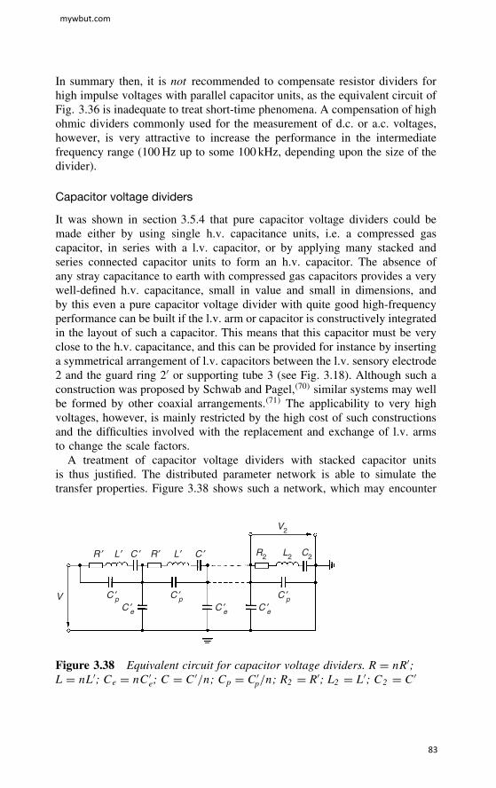
In summary then, it is not recommended to compensate resistor dividers forhigh impulse voltages with parallel capacitor units, as the equivalent circuit ofFig. 3.36 is inadequate to treat short-time phenomena. A compensation of highohmic dividers commonly used for the measurement of d.c. or a.c. voltages,however, is very attractive to increase the performance in the intermediatefrequency range (100 Hz up to some 100 kHz, depending upon the size of thedivider).
Capacitor voltage dividers
It was shown in section 3.5.4 that pure capacitor voltage dividers could bemade either by using single h.v. capacitance units, i.e. a compressed gascapacitor, in series with a l.v. capacitor, or by applying many stacked andseries connected capacitor units to form an h.v. capacitor. The absence ofany stray capacitance to earth with compressed gas capacitors provides a verywell-defined h.v. capacitance, small in value and small in dimensions, andby this even a pure capacitor voltage divider with quite good high-frequencyperformance can be built if the l.v. arm or capacitor is constructively integratedin the layout of such a capacitor. This means that this capacitor must be veryclose to the h.v. capacitance, and this can be provided for instance by insertinga symmetrical arrangement of l.v. capacitors between the l.v. sensory electrode2 and the guard ring 20 or supporting tube 3 (see Fig. 3.18). Although such aconstruction was proposed by Schwab and Pagel,70 similar systems may wellbe formed by other coaxial arrangements.71 The applicability to very highvoltages, however, is mainly restricted by the high cost of such constructionsand the difficulties involved with the replacement and exchange of l.v. armsto change the scale factors.
A treatment of capacitor voltage dividers with stacked capacitor unitsis thus justified. The distributed parameter network is able to simulate thetransfer properties. Figure 3.38 shows such a network, which may encounter
V2
V
R2 L2 C2
C ′pC ′p
R ′ C ′ C ′R ′L ′ L ′
C ′pC ′eC ′eC ′e
Figure 3.38 Equivalent circuit for capacitor voltage dividers. R D nR0;L D nL0; Ce D nC0
e; C D C0/n; Cp D C0p/n; R2 D R0; L2 D L0; C2 D C0
mywbut.com
83

all possible passive circuit elements. The actual stacked capacitors are nowsimulated by the capacitance units C0, and L takes into account the inherentinductance. The series resistance R0 may be used to simulate either only smalllosses within the capacitor units C0, or even real resistors in series with theseunits. The small values of stray capacitances in parallel to the stacked columnsC0
p and to ground C0e complete the equivalent circuit.
A glance at the unit step response, which is represented as
gtt D 1 Ce
6C C CpC 2 expat
1∑kD1
1kcoshbkt C a
bksinhbkt
AB,
where
A D(
1 C Cp
CC Ce
Ck2)2
), a D R
2L,
B D(
1 C Cpk2)2
Ce
), bk D
√k2)2 Ð A
LCeB, 3.87
shows a close similarity to the USR of resistor dividers, eqn (3.75). Bothequations are actually the same, if the value C in eqn (3.87) approaches infinitevalues. With finite values of C, representing capacitor voltage dividers, themain difference is at first related to the negative term Ce/6C C Cp ¾D Ce/6C,which is independent of the time and thus also the frequency. This term wasalso found in the treatment of the ‘equivalent capacitance’, see eqn (3.31). Itappears again as a result of our procedure of the normalization of the USR.All explanations referring to the proper dimensioning of stacked capacitors,therefore, also apply to this result, which demonstrates the possible variationsof the ratio n with Ce.
The time dependency of the USR for ‘pure’ capacitor dividers, i.e. withR D 0 in the equivalent circuit, is obviously very complex. In eqn (3.87),with R D 0, the damping term expat will be equal to 1, and all hyper-bolic functions are converted to trigonometric ones. The numerical evaluationof this equation for this case is impossible due to the infinite number ofsinusoidal terms. It is also not realistic to assume no resistance at all, asat least the (frequency-dependent) dissipation factor of the dielectric willcause some damping. For a simple series equivalent of a lossy capacitor, thisdissipation factor is tan υ D ωR0C0 D ωRC. The relaxation phenomena withinthe dielectric materials, however, control in reality this dissipation factor forhigh frequencies. It has been confirmed by measurements72 that an adequatelow-resistance value can be assumed to evaluate eqn (3.87) as was done inFig. 3.39. Here, the oscillations can be related to the travel time 8 D p
LCe,as a step voltage applied to the input of such a ladder network can travel along
mywbut.com
84

4
3
2
1
010 50 100t (ns)
−1
C = 150 pF; L = 2.5mH; R = 20ΩCe = 40 pF; Cp = 1pF
gt(
t)
Figure 3.39 Calculated unit step response for a capacitor voltage divider;the equivalent circuit is Fig. 3.38. R D 20 ; L D 2 .5 µH; C D 150 pF;Ce D 40 pF; Cp D 1 pF
the column. If the voltage amplitude is not reduced to a zero value when thewave reaches the earthed l.v. part, it will be reflected and excites oscillations.
Pure capacitor voltage dividers are therefore sensitive to input voltages withshort rise times and the output voltage may oscillate with non-oscillating inputvoltages. In addition, such a capacitance divider within the whole measuringcircuit, i.e. with leads connected to its input, will form a series resonant circuit.Thus it is obvious that pure capacitor dividers are not adequate to measureimpulse voltages with a steep front (front-chopped lightning impulse voltages)or any highly transient phenomena (voltage during chopping). Crest values ofswitching impulse or even full lightning impulse voltages, however, can beproperly recorded, if the transient phenomena during the front of the impulseshave disappeared.
The similarity of the step response equations for resistor voltage dividersto those treated in this part stimulated Zaengl to propose and to realize thepossible improvement of pure capacitor dividers by inserting real resistor unitsin series with the capacitors.72 If the value of these resistors is not toohigh, but just sufficient to damp the oscillations, it is likely to achieve anexcellent transient performance. A very similar equation to that of eqn (3.83)could be derived by calculating the transition from hyperbolic to trigonometricfunctions for the argument bk and k D 1 in eqn (3.87), providing again acritical resistance. Such a critical value can also be identified in Fig. 3.40,in which some calculated step responses according to eqn (3.87) are shown.Adequate values for a capacitor voltage divider for a voltage of about 1 MV(height ³ 3 m) are used for this simulation.
mywbut.com
85

1.5
1
4
3
2
1
0.5
0 20
t (ns)
g t (t)
40 60 80 100
Figure 3.40 Computed unit step response Gtt for damped capacitordividers according to equivalent circuit, Fig. 3.38
C D 150 pF; L D 2 .5 µH; Ce D 40 pF ; Cp D 1 pF
(1) R D 250
(2) R D 750 4
√LCe
D 1000
(3) R D 1000 (4) R D 2000
The influence of the magnitude of the resistance R is obvious. A very well-damped response is reached by a resistance value of about
R ³ 4
√L
Ce3.88
although the larger overshoot observed with lower values can still be accepted.The short response time is in accordance with the theory. T0 or T can becalculated by the transfer function as well as from eqn (3.87). It is equivalentto eqn (3.79), and thus T0 D RCe/6. The small resistor values as necessary todamp the oscillations are responsible for these low response times, and thusa ‘series-damped capacitor divider’ is formed. The input impedance of thesedividers increases with decreasing frequencies, and hence the loading effect ofthe voltage generating system is limited. Their application for a.c., switchingor lightning impulse voltages without any restrictions is, therefore, possible.
mywbut.com
86

If a parallel branch of high ohmic resistors is added, d.c. voltages can also bemeasured as shown before and an ‘universal voltage divider’ is formed.
These ‘series-damped capacitor dividers’ are not limited in the voltagerange, as a stacking of capacitor units is not limited as well as the insertionof distributed resistors. These resistors are not heavily loaded, as only tran-sient input voltages cause displacement currents. A ‘general-purpose’ voltagedivider is therefore available, and have been in general use since about 1970up to the highest voltage levels.54,122
Figure 3.41(a) shows such a voltage divider for a lightning impulse voltageof 6 MV. The electrodes are not provided to shield the divider, i.e. to reduceCe, but only to prevent discharges and thus to increase the flashover voltagefor switching impulses.
3.6.5 Interaction between voltage divider and its lead
The analytical treatment of our measuring system presented so far is not yetcomplete. Whereas the USR of the voltage dividers could readily be calculated,similar results are missing for the entire circuit. Now it can be shown that thegeneralized expression for the response time T and its interaction with thecircuit elements, eqn (3.66), can effectively be applied in practice.
As already mentioned in section 3.6.3, it is too difficult to apply an analyt-ical solution to the USR of the whole measuring system, which was repre-sented by the ‘three-component system’ of Fig. 3.29. Numerical solutions byadvanced programming, however, are possible, and many computer programsare available. The results presented here are calculated with the ‘transientnetwork program’ published by Dommel.73 Within this program, the loss-less transmission line (see 2, Fig. 3.29) is simulated by the exact solution ofthe partial differential equations of a line and thus does not introduce anyerrors. The simulation of the terminating system, i.e. the voltage dividers,needs, however, a subdivision of the distributed parameter networks into afinite number of sections. If the number of elements n (for n see Fig. 3.31) islarger than about 5, the results are close to the infinite number solution.
Numerical computations need numerical values for the surge impedance ofthe lead ZL to the divider. For the common set-up of a voltage testing system(Fig. 3.22), this lead is more or less horizontal above the ground return, whichis assumed to be an extended plane. Many experiments50 demonstrated thatthe travel time 8L is controlled by the velocity of light c0. As ZL D p
LL/CL
and 8L D pLLCL D l/c0, with LL being the total inductance and CL the total
capacitance of this lead, ZL D l/c0CL, with l being the length of the lead. Thecapacitance of the lead can be computed assuming that a cylindrical lead ofdiameter d is at height H above a plane, which is earthed. The well-known
mywbut.com
87

Figure 3.41 Series-damped capacitor voltage divider for 6-MV impulsevoltage (courtesy EdF, Les Renardieres, France)
mywbut.com
88

capacitance formula
CL D 2)ε0l
A;
where
A D ln
2l
d
√√√√√√
f1 C 2H/l2g 1√f1 C 2H/l2g C 1
D ln(
4H
d
) ln
1
21 C
√1 C 2H/l2
may well be used, although this lead is placed between the test object andthe voltage divider. As c0 D ε0?00.5, where ε0 D permittivity and ?0 Dpermeability of free space, the surge impedance becomes
ZLhor D A1
2)
√?0
ε0D 60 ð Al, d, H [] 3.89
for this horizontal lead. Sometimes, the horizontal lead is lengthened by avertical lead to measure the experimental USR of the system. Thus we need ZL
for a vertical lead also. According to Fig. 3.22 and eqn (3.33), this capacitanceis known. With the same assumptions as made above, we obtain
ZLvert D 1
2)
√?0
ε0ln
2l
d
√4s C l
4s C 3l
³ 60 ln(
1.15l
d
)[] for s − l. 3.90
The differences in the surge impedances are not large if the usual dimensionsare taken into account.
In Fig. 3.42(a), a very simplified equivalent circuit represents a 20-kresistor divider with a lead length of 3 m (8L D 10 ns). The divider is ideal-ized by the omission of any stray capacitances or inductances, but a parallelcapacitance of Ct D 50 pF across the whole divider represents a top electrodewhich may shield the divider. A pure resistor Rd provides ideal dampingconditions for travelling waves. Figure 3.42(b) shows some computed resultsof the USR. For Rd D 0, no noticeable damping effect is observed within theexposed time scale. Although the oscillations are non-sinusoidal, the funda-mental frequency can clearly be seen. This frequency is obviously close to theresonance frequency fr , generated by the lead inductance LL and the divider’scapacitance Ct. As LL D ZL8L, this inductance is 3 µH, giving fr D 13 MHz.
mywbut.com
89

RdRd variableZL = 300 ΩτL = 10 nsCt = 50 pFRt = 20 kΩR2 C2 = Rt Ct R2 Rt
ZL ; τL
Ct
C2
Rt
R2 gt (t )
2
1.5
1
0.5 450 Ω
300 Ω
150 Ω
Rd = 0
g t (t)
0 10 100
(a)
(b)200
t (ns)
300
<<
Figure 3.42 Computed unit step response for idealized resistor orparallel-mixed resistor–capacitor divider with lead. (a) Equivalent circuit.(b) Computed USR
Thus, this example also implies the typical USR for pure capacitor or parallel-mixed resistor–capacitor voltage dividers, as Ct can well be assumed to repre-sent these types of dividers. Higher values of Ct will decrease the frequencyof the oscillations. Acceptable responses are only provided by a damped lead.To prevent any overshoot, Rd must be close to ZL. The exponential increasein the front and increase of the response time T0 or T D T0 8L is obviouslyproduced by the time constant RdCt, which equals 15 ns for Rd D ZL and thespecific values assumed. Large capacitor dividers with stacked capacitor unitscomprise in general much higher capacitance values, and in such cases thelarge response time of such measuring systems is produced by the necessarydamping of the lead.
We may easily compute T0 or the actual response time T D T0 8L fromeqns (3.66) to (3.71). It is clear that for this ideal divider Tt D 0 and Tkd D 0(no frequency dependency of Zds D Rd). With the only frequency-dependent
mywbut.com
90

term for the input impedance of the divider Zts D Rt/l C sRtCt, we mayeasily find that Tkt D RtCt/1 C ZL/Rt). The final result may be best repre-sented in the form
T D T0 8L D 1
1 C Rd/Rt
[RdCt 8L
(1 ZL
Rt
)(1 Rd
ZL
)]. 3.91
Some remarkable findings can be observed.For Rd D ZL, the length of the lead has no influence upon the response
time. This case corresponds to the ‘infinite line response’, as the same resultwould be achieved if a step voltage supplied from an extremely long leadwould be applied to the dividing system.
With no damping resistance, or Rd < ZL , the response time taken from theactual beginning of the USR will always decrease proportionally with the leadlength l D 8Lc0. This decrease of T is clearly produced by an overshoot ofthe USR. As is seen from the computed USR, the determining factor is RdCt
providing a positive contribution to T. For capacitor dividers, Rt ! 1 andthe same equation can be applied.
A second example (Fig. 3.43) simulates a pure resistor divider of low resis-tance value (2.32 k), which was in reality built from carbon compositionresistors to achieve extremely low values of inductances. The stray induc-tances are therefore neglected in the equivalent circuit (Fig. 3.43(a)), but itcomprises distributed stray capacitances to earth, which have been calculatedwith eqn (3.33). The small input capacitance (5 pF) was estimated as onlya very small top electrode was provided. The voltage divider was used forsteep-front voltage measurements up to 800 kV. The lead length of 6 m wasused for USR measurements only, and the equivalent circuit simulates thislead length. The computed USR (Fig. 3.43(b)) shows again larger oscillationswith no damping resistance in the lead. The traces of the oscillations deviatestrongly from the USR of a pure resistor network (see Fig. 3.30), due to thestray capacitances involved. Only the ‘infinite line response’ is smooth. ForRd D 100 , the computed input voltage of the divider is also plotted to showthe distortion introduced by the divider. The small capacitive reflection ismostly suppressed by the divider.
For this equivalent circuit, again the general dependency of the responsetime from the circuit parameters can be computed by eqn (3.66). The result is
T D T0 8L D 1
1 C Rd/Rt
ð[
RtCe
6C Rd
(Cp C Ce
2
) 8L
(1 ZL
Rt
)(1 Rd
ZL
)]. 3.92
Some interesting findings are observed.
mywbut.com
91

Rd
Rd = 0
(gt ) input
(gt ) input
ZL ; τL
R ′t = 232 Ω; R ′t = 2.32 kΩ ; R ′t ; ZL = 272 Ω
τL = 20 ns
Rt = ∑ Re <<
C ′e = 5 pF; C ′e = 25 pF;Ce = ∑
CpR2 gt (t )(5 pF)
5 elements
100 Ω1.5
0.5
0 20 100 300
t (ns)
g t (
t)
500
1
272 Ω
500 Ω
R ′t
C ′e C ′e
R ′tR ′t R ′t −R2
(a)
(b)
Figure 3.43 Computed USR for low-value resistor voltage divider.(a) Equivalent circuit. (b) Computed USR (for divider input)
The influence of the lead on the divider (8L) is the same as before. Nowthe the divider’s response time (RtCe/6 D Tt appears, as expected. Only apart of the stray capacitance Ce, but the full value of the input capacitanceCp, provides positive response times if the lead is damped.
Figure 3.44 shows oscillograms of measured responses. The lead was placedparallel to the ground and the unit step voltage generator was mounted at thewall of the laboratory, which was shielded by a Faraday cage. There is a verygood agreement between the computed and measured values, the USR and theresponse time.
Finally, the third example (Fig. 3.45) explains the existence of a real timedelay between the output and input voltage of a resistor voltage divider.This example is similar to the first one, but the resistors are distributed andcomprise a small inductive time constant of Lt/Rt D 5 ns. Stray capacitancesin parallel to each section, however, are neglected. The USR of the output
mywbut.com
92

Rd = 0 Rd = 100 Ω
Rd = 500 Ω
50 ns/div.
Rd = 297 Ω 50 ns/div.
50 ns/div.
50 ns/div.
Figure 3.44 Measured unit step response for the resistor voltage divider.R D 2320 , with 6-m lead, according to Fig. 3.43
Rd(gt) input
ZL = 270 ΩtL = 20 ns 65pF
L′t L′t L ′t − LuR ′t R ′t − Ru
C′eRuLu
gt (t)
4 sectionsR ′t = 2k Ω; Rt = 20kΩ; Ru = 20ΩL ′t = 10mH; Lt = 100mH; Lu = 0.1mH(Lt /Rt = Lu /Ru = 5 ns)C ′e = pF; Ce = 5 pF;
Rd = 100 Ω
0 20 100 300 500 700t(ns)
0.5
1
1.5
g t (t)
270 Ω
500 Ω
(gt) input
Figure 3.45 Computed USR of resistor divider with inductance
voltage now starts with a time delay of about 15–20 ns related to the inputvoltage. This delay is caused by the travel time of the divider, 8t D p
LtCe,which is about 22 ns. A stray capacitance C0
p would only theoretically suppressthis travel time, as was shown in reference 50. The very small Ce valuesassumed in this example should simulate a very good shielded divider. Thisrise time of the response is accordingly quite short. If the response time is
mywbut.com
93

calculated as before, an additional small negative term within the brackets(eqn (3.92)) would appear, being RdLt/Rt2. Whereas this term is negli-gable, the additional time delay decreases the computed response time of thedividers, RtCe/6. This effect may thus be taken into account by a reductionof this value by a factor of 3/4, and for this some standards6 recommenda theoretical contribution of the response time for resistor dividers accordingto RtCe/8.
Although many other investigations54 have confirmed the validity of suchanalytical treatments, a theoretical treatment alone will not satisfy the actualneeds. In practice, an experimentally performed step response measurementhas to prove the performance of the systems used, as insufficient constructionsmay show worse results. There are still some unsolved problems inherent toresponse measurements, but they shall not be treated here in detail. The mostdifficult problem is related to the fact that the actual ‘input terminals’ of ourvoltage measuring system (Fig. 3.22) are separated by a long distance due tothe dimensions of the test object. But the existence of a step voltage with a risetime of one nanosecond or less cannot be defined by an electrostatic potentialdifference between points the distance of which is in the metre-range, dueto the basic theory of electromagnetic phenomena. But we still may assumethat actual currents charging the test objects within a short but finite time willproduce a quasi-stationary field and through it a potential difference for whichthe expression ‘voltage’ is justified.
With such restrictions in mind, which are usually neglected, the measure-ment of the step response belongs now to the routine procedure of an ‘accep-tance test’ for an ‘approved measuring system’ as used for the measurementof lightning and even switching impulses, see reference 53. The step volt-ages are usually produced by small generators for some hundred volts, andsome different circuit arrangements can nowadays be used to measure thestep response. Although some further details can be found in the relevant IECStandard,53 some additional information is presented in Fig. 3.46. In this
a
b
c
f
g
d
e
Rd
Figure 3.46 The unit step method. (a) To d.c. supply. (b) Charging resistor.(c) Fast switch. (d) (Added) vertical lead. (e) High-voltage lead. (f) Voltagedivider. (g) To recording instrument
mywbut.com
94

figure, a so-called ‘square loop arrangement’ is shown as recommended bythe earlier standards.6,57 The step generator a to c must have approximatelyzero impedance while generating the voltage step and during the subsequentresponse. Any fast switching device, c, which short-circuits a constant d.c.voltage as used to charge the measuring system before the short-circuit occursis applicable. Very suitable switches are mercury-wetted relays but also auniform field gap of about 1 mm spacing at atmospheric air or a uniformgap with a spacing up to some millimetres under increased gas pressure. Thegas-insulated gaps can short-circuit after breakdown voltages up to some kilo-volts, but only single events can be produced. Whereas these switches fulfil therequirement for ‘zero impedance’, commercial types of electronic pulse gener-ators are inherent with some 10 ohms of internal impedance which contributeto the damping resistor, see Rd. At least a metallic strip conductor 1 m wideshall serve as the earth return between divider and the step generator. Thelength of the lead, represented by d and e, shall be equal to the length asused during actual impulse voltage measurement, if the response time is anessential parameter during the measurements. If only part e is used duringmeasurements, it would be possible to calculate the relevant response timedue to the theory as shown before and elsewhere.131 To avoid such effects,the step generator shall be placed at a metallic wall. Then the usual lead lengthas applied during voltage tests can be used. This ‘vertical lead arrangement’was introduced by one of the authors60 and is the preferred circuit today.
One of the uncertainties of the unit step method is related to the startingpoint, i.e. the value of 8de in Fig. 3.26, of the response. This starting pointon the ‘toe’ region is influenced by electromagnetic waves radiated from theleads between the step generator and the divider. These phenomena havebeen thoroughly investigated by an International Research Group;50 themethods for the computation of these phenomena are based upon Maxwell’sequations, which can either be solved in the time domain76 or in the frequencydomain.77 The solutions are very sophisticated and cannot be treated withinthis chapter. The new IEC Standard,53 however, accounts for these effectsby defining a ‘virtual origin O1’ of the USR together with an ‘initial distortiontime T0’, the definitions of which may be found in this standard.
3.6.6 The divider’s low-voltage arm
We assumed for the theory of dividers, section 3.6.4, that the low-voltage armis an integral part of the divider and provides an impedance structure which isequivalent to the high-voltage arm. In reality, the structure, i.e. the compositionof the circuit elements, is quite different. Therefore, some additional problemsmay appear concerning adequate construction and layout of the l.v. arm ofour measuring system. Many distortions in the response can be related to thispart of the system.
mywbut.com
95

For d.c. and a.c. voltage dividers, the design of the l.v. arm is not critical, ifonly steady state voltages have to be recorded. However, if any fast transientshave to be transmitted from the voltage divider to the recording instrument(see Fig. 3.23, items 5 to 7), the l.v. arm of the voltage divider itself mayintroduce large disturbances to the response. Let us first discuss the adequateimpedance matching necessary to transmit impulse voltages from the dividerto the recording instrument.
In Fig. 3.47 the somewhat simplified equivalent circuits for the matchingprocedures for the different types of dividers are sketched. The signal cable ismainly treated as lossless, so that the surge impedance Zk D p
Lk/Ck becomesindependent of frequency, and the travel time 8k D p
LkCk is a plain value.For resistor voltage dividers, Fig. 3.47(a), the cable matching is simply doneby a pure ohmic resistance R D Zk at the end of the signal cable. The trans-mission line theory provides the well-known background for this procedure,the reflection coefficient becomes zero and any unit step voltage appearingacross R2 is undistorted transmitted by the cable. As the input impedance ofthe signal cable is R D Zk , this resistance is in parallel to R2 and forms anintegral part of the divider’s l.v. arm. The low-value of this resistance R, i.e.typically 50 to 75 , should in fact suggest that we consider the losses of thesignal cable. These losses are in reality dependent upon frequency due to theskin effect, and the response of such a cable becomes very complex. Whereasthe theory of this problem may be found elsewhere,124,125 the result of thistheory shows clearly that the best matching can be achieved with R equal tothe surge impedance Zk defined for high frequencies. For all kinds of signalcables the d.c. resistance for the conductors (inner conductor and shield) willform a voltage dividing system between R2 and R, which may decrease thevoltage across R by an amount of 1 per cent in order of magnitude. As thisamount can easily be taken into account by d.c. resistance measurements only,this value should be taken into account. The unit step response from a lossycable is characterized by a steep increase within a few nanoseconds to valuesof more than 90 per cent and a slow tripling up to the final value. Theseeffects will introduce larger errors if the impulses to be transmitted are shorterthan 0.5 to 1 µsec. At least an experimental test is recommended to check thesignal cable with regard to this additional error.
For parallel-mixed resistor-voltage dividers the same procedure for cablematching, Fig. 3.47(a), applies. A matching resistor R, coaxially designedto meet the high-frequency requirements, will not reflect energy. The inputimpedance of the recording instrument, however, should not comprise appre-ciable input capacitance, as otherwise too heavy reflections will appear. Thel.v. arm for this type of divider reflects heavily due to the parallel capacitanceto R2.
For capacitor voltage dividers, Fig. 3.47(b) or (c), the signal cable cannotbe matched at its end. A low ohmic resistor in parallel with C2 would load the
mywbut.com
96

R1
R = Zk R = Zk
C1
R2Ck
(a) (b)
(c) (d)
Zk ; τk
C2
R3
C4
R4
C1
C2
C1
Zk ; Ck
Zk; Ck Zk; Ck
(Zk− R2)
C2
R1
C1
R2
C2
CRO CRO
CRO CRO
Figure 3.47 Circuits for signal cable matching. (a) Resistor orparallel-mixed capacitor-dividers. (b) Capacitor dividers, simple matching.(c) Capacitor dividers, compensated matching. (d) Damped capacitor divider,simple matching
l.v. arm of the divider too heavily and decrease the output voltage with time.To avoid travelling wave oscillations, the cable must then be terminated at itsinput end. Then, a voltage step of constant amplitude at C2, i.e. C2 ! 1, willbe halved by R D Zk at the cable input end, as R and Zk form a voltage divider.This halved voltage travels to the open end and is doubled by reflection. Thusthe original amplitude of the voltage across C2 appears at the input of therecording instrument. The reflected wave charges the cable to its final voltageamplitude, and is absorbed by R, as the capacitor C2 forms a short-circuit. Inreality, C2 is of finite value and is therefore discharged during these transientevents. The computation shows that the discharge period is very close totwice the travel time. After this time, the cable capacitance is charged tothe final voltage, and from this we obtain two ratios of the voltage divider,namely:
no D C1 C C2
C1for t D 0;
ne D C1 C C2 C Ck
C1for t ½ 28k.
mywbut.com
97

The signal cable, therefore, introduces an initial ‘overshoot’ of the voltage ofV D ne/no 1 D Ck/C1 C C2, which may well be neglected for shortor medium cable length and high values of C2, i.e. high ratios of the voltagedividers.
But capacitor dividers are often used for field testing of transient voltagesand longer cables thus are often necessary. The response can be improved bytransferring a part of the l.v. capacitor C2 to the cable end and connecting itin series with a resistor, Fig. 3.47(c). This system, first treated by Burch,120
offers some opportunities to decrease the overshoot effect. Burch proposed tomake both matching resistances equal and R3 D R4 D Zk . If then the conditionC1 C C2 D C3 C Ck is satisfied, the initial and infinite time values of thevoltage become the same, and the original overshoot of about Ck/Cl C C2is reduced to about 1/6. There are, however, further opportunities to improvethe response as shown by Zaengl.121
From high voltage arm
From high voltage arm
Circuit elements
(R2, C2)
Circuit elements
(R2, C2)
Metal housing
Metalhousing
Matching impedance,if necessary
Matching impedance,if necessary
Signal cableconnection
Signal cableconnection
Cu-disc, silver plated
Figure 3.48 Sketched cross-sections of possible layouts for the l.v. arm ofvoltage dividers
mywbut.com
98

For damped capacitor dividers, the resistors R1 and R2 necessary within thel.v. arm are for the reflected wave in series to the matching impedance at thel.v. arm, see Fig. 3.47(d). As R2 is very small in comparison to R1, the valueof this matching resistor must only be reduced by the small value of R2. Themethods of Fig. 3.47(c) can also be applied.
Whereas matching resistors for coaxial cables, i.e. resistors between innerand outer conductors, are commercially available, the series resistors for allcapacitor dividers are an integral part of the divider’s l.v. arm. It may well berecognized that the path to earth for the reflected wave should not be hinderedby too high inductances. This condition dictates the need for every l.v. capac-itor to have a very low inductance. The theoretical value of this inductance isgiven by the ratio of the divider, which divides also the overall inductance ofthe stacked capacitor column. The physical size of the capacitance C2 valuesnecessary to reduce the high-voltage to a measurable quantity is, however,relatively large. The coaxial arrangement of any circuit elements used withinthe l.v. arm is a condition which should be strictly followed. In Fig. 3.48simple cross-sections of possible layouts of the l.v. arm are sketched. Radi-ally arranged elements tend to give even lower inductance values. The metalhousing avoids the impact of electromagnetic fields. By the coaxial connectionof the original cable, the input loop of this cable will not ‘see’ any effectivemagnetic field, which contributes to reduced voltages by the transient currents.Therefore, the current paths must be evenly distributed within the coaxiallyarranged elements. A too low inductance may easily be increased by the addi-tion of small wire loops in series with the elements. For more informationreference should be made to the literature.123,126
3.7 Fast digital transient recorders for impulsemeasurements
With the advent of high-speed digital recorders the field of high-voltageimpulse testing has gained a powerful tool. Recent technological developmentshave made the use of digital recorders possible in the field of high-voltageimpulse measurements.78–84 Their use has important advantages over the useof traditional analogue oscilloscopes and recorders. Obtaining impulse testrecords in digital form allows for the introduction of the wide range of digitalsignal processing techniques into the analysis of high-voltage test data. Thesetechniques enable high-voltage test engineers to correct errors due to non-ideal voltage dividers, to eliminate the effects of slight variations in the formof applied impulses in successive test records, to analyse test object transferfunctions rather than merely visually examine the forms of applied stimuli andrecorded responses, and to perform statistical analyses on the results of longseries of impulse tests.85–89
mywbut.com
99

Although digital techniques have been available for many years, it is onlyover the last decade that their use for measurements in high-voltage impulsetests has become widespread: all the standards covering digital recorders havebeen published in the last twelve years. Digital recorders for general use arecovered by IEEE Std 1057-1994:135 there are no IEC Standards which coverdigital recorders for general use. There are presently two standards that dealwith digital recorders for measurements in high-voltage impulse tests: IEEEStd 1122-1998136 (revision of IEEE Std 1122-1987) and IEC document 1083-1: 1991137 (a revision is being prepared based on IEEE Std 1122-1998).These standards define terms, identify quantities that affect accuracy, describetests and set minimum standards to be met by each tested parameter. In manycases, it is not possible to isolate one parameter and test it alone and hencethe limits have to allow for other contributions, e.g. noise on the record. Manytest engineers make use of these standards to make a preliminary selection ofdigitizers based on the manufacturer’s specifications but the selected digitizerhas then to be tested according to the standard. The standards set limits on thesampling rate and the rated resolution. In addition limits are set on measuredvalues of integral non-linearity of the amplitude and the time base, the differ-ential non-linearity of the amplitude, the impulse scale factor, the rise time,the internal noise level, and the effects of interference and ripple.
The following sections of this chapter review the development andfundamental operating principles of digital recorders, outline how thesedevices differ from their analogue predecessors, cover the sources of staticand dynamic errors inherent in digital recorders, and finally provide insightinto the test procedures and minimum performance requirements mandated incurrent standards136,137 related to the use of digital recorders in h.v. impulsetesting.
3.7.1 Principles and historical development of transient digitalrecorders
The first attempts at digital recording of non-repetitive pulses were under-taken in the late 1950s in order to enable on-line processing of recordedtransients. Research in nuclear physics and radar signature analysis promptedthe design of a hybrid oscilloscope–TV camera system, which employed aconventional high writing-speed CRT coupled to a television vidicon tubescanning the CRT screen. Although very useful in this pioneering period,this hybrid recorder combined the drawbacks of both analogue and digitalsystems. However, the concept of fast writing on a temporary storage mediumand scanning this medium later at a slower rate was a valuable innovation,and the hybrid recorder paved the path to more refined designs. This ideaspawned the development of recorders which formed the functional basis ofpresent day scan converters. In the late 1970s electronic circuits utilizing solid
mywbut.com
100

state components for high-speed analogue-to-digital conversion came into use.Since then several other mechanisms for realizing the A/D conversion processhave been implemented.
The recording errors which characterize a recorder’s dynamic accuracydepend to a certain extent on the design and operating principles of theinstrument.90–93 To gain an understanding of the physical principles respon-sible for these errors it is useful to review briefly the various available designsof recorders. There are four basic A/D conversion schemes utilized in presentday high-speed digital recorders. These are: scan conversion, charge coupleddevice storage, flash conversion, and ribbon beam conversion.
Scan converters
The highest speed A/D conversion technique presently available utilizes scanconverters. These consist essentially of an analogue cathode ray tube withthe electron beam writing on a matrix of precharged semiconductor elements.The moving electron beam leaves a trace of discharged elements on the targetmatrix. The target is then read by another beam which scans the matrix at aslower pace. The slowed down replica of the recorded transient is digitized bya conventional ADC and stored for further display and processing. The mainerrors in such an instrument come from the difference between the electronbeam writing speed at the steep and flat portions of the recorded transient.The variation in writing speed results in blooming or thickening of the tracein its slower portions similar to that often encountered in storage oscilloscopeswhen recording transients with slow and fast portions. However, with a scanconverter, data processing can be used to reduce errors caused by bloomingand the instruments can achieve a vertical resolution of approximately 1 percent at a sweep of 5 ns. Further errors are generated by variations in the timebase. In addition to these drawbacks, short record length is a limitation inherentin this recording technique. Despite these shortcomings, scan converters areused in many laboratories where high bandwidth and very high equivalentsampling rates are needed.94
Charge coupled device converters
Development of the charge coupled device (CCD) formed the basis of anotherfast digitizer. The CCD input of such a digitizer (often referred to as thebucket-brigade circuit) consists of a number of capacitors and electronicswitches integrated on a chip and driven by a clock which can operate ata fast and a slow rate. The first sample of the transient to be recorded istaken by connecting the first capacitor to the instrument’s input terminal for ashort period. At the next stage, the charge accumulated in the first capacitor istransferred to the second one and the first capacitor is discharged in preparationfor the next sample. This procedure is repeated at the high clock rate until the
mywbut.com
101

first sample is transferred to the last capacitor. This completes the recordingcycle and the recorded transient is stored in the form of charges accumulatedin each of the capacitors contained in the CCD. In order to read the signal, thebucket-brigade charge transfer process is repeated in the reverse direction at theslow clock rate. The subsequent samples are then digitized by a conventionalADC at the output terminal of the CCD and stored in the memory for furtherprocessing.
By using an advanced control system several MOS integrated circuit regis-ters can be charged sequentially at a high rate thereby increasing the availablerecord length. Although the output signal from the registers can be digitized(at a slower rate) with high resolution, the actual gain accuracy of CCD-basedrecorders is limited to approximately 1 per cent which is often much less thanthe high resolution of the actual slow sampling rate A/D converter.95 Thislimit is set by the analogue techniques of sampling the recorded transientswith CCD elements.
Flash converters
The third type of fast digitizer is based on the conventional flash conver-sion technique implemented in advanced semiconductor technology.96,97 Inhigher resolution instruments two low-resolution monolithic flash convertersoperating at very high sampling rates are used in a subranging mode. The tech-nique is known as dual rank flash conversion. The input signal is digitized bythe first ADC and the digital output is fed into a digital-to-analogue converter(DAC). The DAC output is subtracted from the delayed input signal and theresidue is fed into the second ADC to give an overall resolution of doublethat of each ADC used. The principal limitation of this digitization schemeis the time required for the DAC to settle so that the subtraction yielding thesecond ADC’s input can be performed with sufficient accuracy. This sets thelimit on the maximum sampling rate of dual rank flash converters.
A variation of the flash conversion technique can be implemented by usingtwo high-resolution but slower sampling rate ADCs to sample the input alter-nately, thus giving an effective sampling rate of twice that of each ADC. Inthis type of digitizer additional errors can arise from differences in the quanti-zation characteristics of the two ADCs and/or from asymmetry in the samplingintervals.
Ribbon beam converters
The last design principle used in digital recorders to achieve high resolutioncombined with high sampling rate incorporates an electron bombardedsemiconductor (EBS) tube.98 The EBS tube is similar to a conventionalcathode ray tube (such as those used in analogue oscilloscopes) except that theluminescent screen is replaced by a target made up of a set of N adjacently
mywbut.com
102

positioned strip diodes. The beam is flat in the horizontal plane like a ribbonrather than being focused to a point, and there is only one set of plates usedto deflect the electron beam. A metal mask, installed between the electronbeam and the diode target, has a pattern of windows cut in it so that as thehorizontal beam moves up and down with the input signal it illuminates variouscombinations of exposed diodes. A maximum of 2N unique combinations ofthe N diode states are available. The output of each diode strip is checkedat an interval corresponding to the recorder’s sampling rate to generate anN-bit binary encoded word which corresponds to the level of the input signalpresent at the instant that the diode outputs are checked.
Although the different high-speed digital recorders described above mayappear similar from the input/output perspective the different conversionschemes can introduce different errors. In fact, the errors obtained using a high-speed recorder are in many instances a direct consequence of the conversiontechniques implemented in the particular instrument. In order to assess theactual measuring properties of a digitizer, it is therefore important to examinenot only the sampling rate and resolution, but also the type of A/D conversiontechnique utilized.
3.7.2 Errors inherent in digital recorders
In contrast to an analogue oscilloscope which writes a continuous trace of themeasured signal, a digital recorder is able to record and store only instan-taneous values of the signal rounded to integer numbers and sampled at acertain rate over a finite period of time. The input signal is reconstructed bypositioning in time (according to the sampling rate) and the vector of consec-utive values contained in the recorder’s memory. This leads to the presence oftwo types of recording errors which are generally referred to as quantizationand discrete time sampling errors. These errors are the only ones present inan ideal recorder. Since they occur even when recording slowly changing oreven d.c. input signals they are often referred to as static errors.
Static errors
The quantization error is present because the analogue value of each sample istransformed into a digital word. This A-to-D conversion entails a quantizationof the recorder’s measuring range into a number of bands or code bins, eachrepresented by its central value which corresponds to a particular digital codeor level. The number of bands is given by 2N, where N is the resolutionof the A-to-D converter. The digital output to analogue input relationship ofan ideal digitizer is shown diagrammatically in Fig. 3.49. For any input inthe range (iVav 0.5 Ł Vav to iVav C 0.5 Ł Vav), where Vav is thevoltage corresponding to the width of each code bin, or one least significantbit (LSB), and iVav is the centre voltage corresponding to the ith code, an
mywbut.com
103

ln
nv
(n-1)∆vav
(n-2)∆vav
(n-3)∆vav
(n-4)∆vav
3 ∆vav
2 ∆vav
0
∆vav
ln -1
ln -2
ln -3
ln -4
l3
l2
l1
l0
DIGITAL OUTPUT
ANALOGUE INPUT
Figure 3.49 Analogue input to digital output relation of an ideal A/Dconverter
Dig
ital o
utpu
t cod
e
Time
Figure 3.50 Response of an ideal A/D converter to a slowly rising ramp
ideal digitizer will return a value of Ii. Therefore, the response of an idealdigitizer to a slowly increasing linear ramp would be a stairway such as thatshown in Fig. 3.50. A quick study of these figures reveals the character ofthe quantization error associated with the ideal A-to-D conversion process.The maximum error possible is equivalent to a voltage corresponding to š 1
2
mywbut.com
104

of an LSB. For an ideal digital recorder, this quantization would be the onlysource of error in the recorded samples. For a real digital recorder, this errorsets the absolute upper limit on the accuracy of the readings. In the case of an8-bit machine, this upper limit would be 0.39 per cent of the recorder’s full-scale deflection. The corresponding maximum accuracy (lowest uncertainty)of a 10-bit recorder is 0.10 per cent of its full-scale deflection.
The error caused by discrete time sampling is most easily demonstrated withreference to the recording of sinusoidal signals. As an example we can lookat the discrete time sampling error introduced in the measurement of a singlecycle of a pure sine wave of frequency f, which is sampled at a rate of fourtimes its frequency. When the sinusoid and the sampling clock are in phase,as shown in Fig. 3.51, a sample will fall on the peak value of both positiveand negative half-cycles. The next closest samples will lie at )/2 radians fromthe peaks. As the phase of the clock is advanced relative to the input sinusoidthe sample points which used to lie at the peak values will move to loweramplitude values giving an error () in the measurement of the amplitude(A) of
D A1 cos #
Figure 3.51 Sample points with sinusoid and sampling clock in phase.(Error in peak amplitude D 0 )
where # is the phase shift in the sample points. This error will increase until# )/4 (Fig. 3.52). For # > )/4 the point behind the peak value will nowbe closer to the peak and the error will decrease for a # in the range of )/4to )/2. The maximum per unit value of the discrete time sampling error isgiven by eqn 3.93,
max D 1 cos)fts 3.93
where ts is the recorder’s sampling interval and f the sinewave frequency.
mywbut.com
105

∆
Figure 3.52 Sample points with sampling clock phase advanced to )/4with respect to the sinusoid. Error in peak amplitude () is at a maximum
The maximum errors obtained through quantization and sampling whenrecording a sinusoidal waveform are shown in Fig. 3.53. The plotted quantitieswere calculated for an 8-bit 200-MHz digitizer.
Err
or
∆MAX OUANT.
∆MAX SAMPL
∆MAX SAMPL
Frequency (MHz)
1
2
1
.4
0
2 3 4 5 6 7 8 10 20
tss/t
Figure 3.53 Sampling and quantization errors of an ideal recorder
In a real digital recorder, an additional two categories of errors areintroduced. The first includes the instrument’s systematic errors. These aregenerally due to the digitizer’s analogue input circuitry, and are present tosome degree in all recording instruments. They include such errors as gain
mywbut.com
106

drift, linearity errors, offset errors, etc. They can be compensated by regularcalibration without any net loss in accuracy. The second category containsthe digitizer’s dynamic errors. These become important when recording high-frequency or fast transient signals. The dynamic errors are often random innature, and cannot be dealt with as simply as their systematic counterparts andare discussed below.
Dynamic errors
In an ideal digitizer each sample of the recorded transient is taken in aninfinitely short time window. This precludes any variation in the width ofthe time window which is often termed aperture uncertainty or jitter. Simi-larly, there is no uncertainty in the time at which the sample is taken. Thewidths of all the code bins are equal, and symmetrical about the level repre-senting each bin’s centre. When a real digitizer is constructed, the non-idealnature of all these parameters comes into play. While their effects can bereduced to a negligible level in recorders characterized by slower samplingtimes, in those digitizers which push today’s technology to its limits so as toprovide the highest resolution coupled with the fastest sampling rates, theseparameters may have a significant effect on the dynamic accuracy of theinstruments.91,93,99–113
The nature, magnitude and consequences of the random errorsencountered in real digital recorders vary depending on the instrument’sdesign.100,114,115,95 As a result the determination of the suitability of aparticular type of recorder to h.v. impulse testing must consist of two phases.The initial phase consists of specifying the sampling rate and resolution ifideal digitizer performance can be assumed. Following this, the dynamicperformance of the recorder under consideration must be determined. Theformer requires that the digitizer’s nominal resolution in bits and samplingrate be related to the accuracies required by the standard for instruments usedin recording h.v. impulses. The latter entails determination of the nature andlimits of the recorder’s dynamic errors. This approach was followed in thedevelopment of IEEE Std 1122136 and IEC Pub. 1083,137 the standardsdealing with qualification of digital recorders for h.v. impulse measurements.
3.7.3 Specification of ideal A/D recorder and parameters requiredfor H.V. impulse testing
Standard impulses used in H.V. testing of power apparatus
Requirements on the accuracy of recording instruments used in high-voltageimpulse testing vary according to the type of tests, and depend upon the natureof the test object itself, e.g. testing and research into the dielectric strengthof gas-insulated substations (GIS) involve generation and measurement of
mywbut.com
107

very steep-front high-voltage impulses which may be chopped after a time asshort as 0.1–0.2 µs. This type of test does not require a very high measuringaccuracy, i.e. an uncertainty of a few per cent on the impulse crest isacceptable. Details regarding impulse testing procedures of testing varioustypes of insulations are described in Chapter 8, section 8.3.1, with appropriatereferences to national and international standards. Definitions of the prescribedstandard voltage waveshape to be used in testing can be found in Chapter 2,Figs 2.23(a) to (c).
Peak measurements
As previously discussed, the maximum ideal quantization error is equal to1 LSB. This can be restated in terms of per cent of full scale as 100/2N,where N is the recorder’s resolution in bits. For the error to be less than orequal to 2 per cent of full-scale deflection a simple calculation shows thatthe recorder’s resolution should be not less than 5.7 bits. This must of coursebe rounded up to the closest integer, 6. Therefore, for a full-scale signal, anideal 6-bit recorder will meet the amplitude accuracy requirement. In practiceit is not possible, or at least not practical, to ensure that all the signals to berecorded will span the instrument’s full measuring range. It is more realisticto assume that the input signals will fall within a range of between 50 percent and 90 per cent of full scale. For a signal which covers 50 per cent ofthe recorder’s full scale, an accuracy limit of 2 per cent would be maintainedby using an ideal recorder of 7-bit resolution. The magnitude of the maximumpossible discrete time sampling error depends upon the shape of the impulserather than on its magnitude. Therefore, the sampling-rate requirement mustbe examined for each different impulse shape. Using the fastest allowablestandard lightning impulse as a basis for calculation, the maximum errors inpeak voltage measurement as a function of the recorder’s sampling rate canbe calculated using the same approach as previously illustrated for the case ofa sinusoidal input. The maximum possible errors resulting from sampling aregiven in Table 3.6.
As can be seen from the tabulated results the discrete time sampling erroris negligible in comparison to the quantization error when recording the peakvalue of a full lightning impulse.
Tests often require the use of chopping the standard lightning impulse waveon the front or the tail as shown in Figs 2.23(c) and (b) respectively. With astandard lightning impulse chopped after 2 µs to 5 µs (tail), since the choppingoccurs after the peak, the analysis used to derive nominal recorder character-istics required for acceptable recording of the peak value is identical to thatoutlined above for the case of the standard lightning impulse.
For testing with front-chopped impulse voltages two cases must be consid-ered. The first of these is termed a front-chopped impulse and the second a
mywbut.com
108

Table 3.6 Maximum error due tosampling when recording the peakof a full standard lightning impulse
Sampling rate Error in % FSD(MHz)
2 0.1952.8 0.0974.0 0.0485.7 0.0248.6 0.012
12.0 0.006
linearly rising front-chopped impulse. As far as the measurement of their peakvalues is concerned these two impulses can be treated under the same analysis.
For impulses chopped on the front, the most demanding situation coveredby today’s standards specifies that the peak value of an impulse with a time-to-chop of 500 ns be recorded with the recording device contributing an errorof less than 2 per cent. In this situation, the discrete time sampling error mustbe considered as well as the quantization error. For an ideal sawtooth input(the limiting case of a front-chopped impulse) the maximum possible discretetime sampling error is given by the product of the sampling interval and thesignal’s rate of rise. This is illustrated in Fig. 3.54.
Values of maximum discrete time sampling error (in per cent of the peakvalue) vs recorder sampling rate are shown in Table 3.7 for the shortest stan-dard time-to-chop of 500 ns.
Table 3.7 Maximum error due to samplingwhen recording the peak of an idealsawtooth waveform with a 500 ns rise time
Sampling rate Error in % of peak value(MHz)
50 4100 2200 1
mywbut.com
109

u
1.0
0.9
0.5
0
E
0.05 Tr
0.05 Tr
Tr / 2.5 t
Figure 3.54 Sampling error for an ideal sawtooth signal
From a comparison of Tables 3.6 and 3.7 it can be seen that the requirementsplaced on sampling rate are far more severe when recording front-choppedlightning impulses than when recording standard full lightning impulses orimpulses chopped on the tail. As shown in Table 3.7, a minimum samplingrate of 100 MHz is required to ensure a discrete time sampling error of 2 percent or less in the measurement of the peak.
In reality high-voltage impulses are rounded at the chop. Figure 3.55 showsan example of a linearly rising impulse applied to a 250 mm sphere gap witha gap length of 60 mm. The slope of such a linearly rising front-choppedimpulse is, according to the standards, taken as the slope of the best fittingstraight line drawn through the portion of the impulse front between 50 percent and 90 per cent of its peak value. The rise time is defined as being thetime interval between the 50 per cent and 90 per cent points multiplied by 2.5.The impulse shown in Fig. 3.55 was measured using a small divider insulatedwith compressed gas and characterized by an extremely low response time.The measured rate of rise of 10.8 kV/ns and time-to-chop of 36 ns are muchmore severe than those typifying standard test impulses. However, even inthis very severe case, the waveshape shows that the slope close to the chop isvery much less than the impulse’s rate of rise as calculated between the 50 percent to 90 per cent points on the impulse front. For higher peak voltages, thatis larger breakdown distances and larger (hence slower) impulse measuringsystems, the rounding effect just prior to the chop will be more pronounced.This means that in practice the slope at the instant of chopping is significantlyless than (Vpk/500 kV/ns. Since this was the figure used in calculating the
mywbut.com
110

0−365
−370
−375
−380
−385
−100
−200
−300
−4000 10 20 30 40 50
Time (ns)
Vol
tage
(kV
)
40 42 44 46 48
Figure 3.55 Actual record of a linearly rising front-chopped h.v. impulse.(Inset shows every fifth sample in the vicinity of the chop)
minimum sampling rates necessary to limit the discrete time sampling errorsto acceptable values, the requirements on the sampling rate can be relaxedfrom those given for the case of the sawtooth wave.
There are two factors responsible for the rounding of the impulse wave nearthe time of chopping. The first is the mechanism of the breakdown which isresponsible for the voltage collapse. Although not in all cases, this mech-anism often contributes a significant amount to the rounding. The second,often more important, factor in rounding the impulse peak is the limited band-width of high-voltage measuring systems. Because of their physical size, thesesystems cannot respond quickly to fast changes in their input. The rounding-offintroduced in the measurement of an ideal sawtooth waveform with a 500 nsrise time is illustrated in Fig. 3.56. The response to such an input is shownfor high-voltage measuring systems of varying response times. The standardsrequire that a measuring system have a minimum response time of 0.05 timesthe rise time of any linearly rising front-chopped impulse which it is used torecord.6,53 In the worst case of a 500 ns rise time this requirement translatesinto a response time of 25 ns or less. Looking at the case of the measuringsystem with 25 ns response time shown in Fig. 3.54 a significant rounding inthe area of the peak is evident.
A simple computer analysis can be used to calculate the values of samplingfrequency which are necessary to meet the 2 per cent accuracy requirement.
mywbut.com
111

1.0
0.8
0.6
0.4
0 .2
00 1 2 3 4 5
f (MHz)6 7 8 9 10
0 0.1 0.2 0.3 0.4 0.5 0.6 0.7 0.8
100
5075
25
Tresponse(ns)
Front-choppedImpulse
T (ms)
Figure 3.56 Illustrative example of a front-chopped impulse(tchop D 0 .5 µs) distorted by an analogue measuring system of a limitedbandwidth. Attenuation of higher spectral frequencies of the impulse by themeasuring system and corresponding distortion of the impulse form areshown for a few values of the response time of the system
However, for the practical case of bandwidth limited measuring systems, theminimum requirements on sampling rate necessary to ensure recording of thepeak are exceeded by those necessary to meet standard requirements on themeasurement of time parameters and front oscillations discussed below.
Measurement of time parameters
Since lightning impulses are defined by time as well as amplitude parameters,the sampling rate required for the evaluation of the time parameters mustalso be determined. As previously stated, the standards’ present requirementon oscilloscopes used to record h.v. impulses is that they must allow for theevaluation of time parameters with an accuracy of better than 4 per cent.As with the determination of minimum sampling rates required to ensurethe specified accuracy in the measurement of the impulse peaks, each type ofimpulse must be examined in turn to derive minimum sampling rates necessaryfor required accuracy in the measurement of time parameters. A standardfull lightning impulse is defined by its front time and its time-to-half value(Fig. 2.23(a)). The front time is defined as 1.67 times the time interval betweenthe instants at which the impulse is between 30 per cent and 90 per cent of itspeak value. To determine the minimum sampling rates necessary to evaluatethe front time to within 4 per cent the fastest allowable standard lightningimpulse must be examined. It is characterized by a front time of 0.84 µs.This means that the shortest time interval which must be measured for suchan impulse is 503 ns. The time-to-half value is defined as the time interval
mywbut.com
112

between the virtual origin (O1 in Fig. 2.23(a)) and the instant on the tail atwhich the voltage has dropped to half of the peak value. The evaluation ofthe time-to-half value entails recording a much greater time interval than thatrequired to determine the front time. Therefore, the requirement on minimumsampling rate is set by the latter. For a standard impulse chopped on the tailthe shortest time interval to be recorded is also the front time and its minimumvalue is the same as that of a standard full lightning impulse. The second timeparameter used to define a chopped impulse is the time-to-chop. However, bydefinition this time interval is between 2 µs and 5 µs, so the minimum requiredsampling rate must be based on the front time measurement. For a front-chopped or linearly rising front-chopped lightning impulse the time intervalbetween the virtual origin (O1 in Fig. 2.23(c)) and the instant of chopping canbe much shorter. The minimum time-to-chop allowed for in the standards is500 ns. This means that the minimum sampling rates required to record thedefining time parameters of full, front-chopped, linearly rising front-chopped,or standard chopped impulses are approximately equal. To evaluate a timeinterval of 500 ns with an accuracy of better than 4 per cent it is necessary tosample at a rate of 500 MHz or more.
Recording of front oscillations
The standard test impulses (Fig. 2.23(a)) are based on pure bi-exponentialwaves such as would be produced by the resistive and capacitive componentspresent in impulse generating and measuring systems. In practical realizationsof large high-voltage systems, there is always some inductance present inthe circuit. This inductance results in oscillations being superimposed on thetest impulses. A typical record of an impulse with superimposed oscillations isshown in Fig. 3.57. As is expected, the maximum frequency of the oscillationsin the circuit decreases as the physical size of the circuit increases.
There are standard requirements placed on impulse test waveforms withregards to the maximum amplitude of superimposed oscillations. In order to
0 2 4 6 8 t (ms)
Figure 3.57 Standard full lightning impulse with superimposed oscillations
mywbut.com
113

ensure that these criteria are met, it is necessary to be able to evaluate thepeaks of the oscillations with a certain precision. The standard requirementintended to ensure sufficiently accurate recording of the oscillations statesthat the upper 3 dB cut-off frequency for surge oscilloscopes be at least twotimes fmax. The oscillations present on impulses are damped sine waves.Therefore, the formula which gives the maximum discrete sampling time erroras a function of signal frequency and sampling rate (eqn 3.93) detailing theerrors of ideal recorders can be applied in this instance. Examination of thisformula reveals that a maximum error of 30 per cent or 3 dB is obtained whenthe sampling frequency is four times larger than the frequency of the sinewave being sampled. Therefore, to correspond to the requirement placed onsurge oscilloscopes (f3 dB > 2fmax) the sampling rate of the recorder must beat least 8 times fmax.
Impulse tests on non-self-restoring insulation
H.V. impulse testing of apparatus such as power transformers, which containnon-self-restoring insulation, often requires using non-destructive test tech-niques. Such tests usually consist of checking the linearity of the test objectinsulation impedance within a range of test voltages up to the basic insula-tion level (BIL).85,116,117,118 The quantities monitored during these tests arethe applied voltage and the neutral current which is taken as the responseto the voltage application. The analysis of test records comprises a detailedcomparison of records taken at different voltage levels. Meaningful devia-tions between the records indicate that the characteristics of the test objectare non-linear, and the test results in a failure. Since even small deviationsbetween records are meaningful and can result in the disqualification of avery expensive piece of equipment, it is imperative that the recorder usedprovides enough accuracy to resolve such differences. Fortunately, the mean-ingful frequency content of the records to be examined is band limited to afew MHz (typically less than 2.5 MHz). The requirements on oscilloscopesused for such tests have never been accurately specified as the same impulseoscilloscope has been used for monitoring tests on self-restoring and non-self-restoring insulation. The parameters of an ideal digitizer which meets therequirements are, therefore, not as easily determined as those of one appro-priate for testing of self-restoring insulation. The derivation of the necessaryparameters can be approached in two ways. The first of these entails matchingthe accuracy of the analogue h.v. impulse oscilloscopes which have becomethe de facto standard instruments for use in these tests.119 The second is toindividually examine all the test procedures and methods of analysis asso-ciated with the testing of objects containing non-self-restoring insulation. Amajor problem encountered in realizing this second alternative stems fromthe fact that different apparatus standards have different requirements which
mywbut.com
114

must be used in the derivation of the required resolution and accuracy of thedigital recorder. This problem causes the latter approach to be less favourablethan the former. The high-quality surge oscilloscopes generally used in h.v.impulse testing are characterized by a bandwidth of approximately 35 MHz.The vertical or amplitude resolution of such an oscilloscope cannot be matchedby an 8-bit digitizer, but it is most certainly exceeded by the resolution of a 10-bit recorder. The minimum sampling rate required for such tests is not clearlyspecified, but can be deduced on the basis of test requirements. When moni-toring tests on power transformers and reactors, the neutral current is usuallyrecorded by means of a shunt whose bandwidth is generally below 3 MHz. Asecond aspect of the test which can shed light on the required sampling rateis that in certain design tests involving the use of chopped waveforms, thetime taken for the voltage to collapse is specified as being between 200 ns and500 ns. The accuracy with which this parameter is recorded is a direct func-tion of the sampling rate of the recorder used. However, at present there isno limit specified on the error permissible in the establishment of the durationof voltage collapse. In order to ensure accuracies superior to those attainablewith presently used oscilloscopes, it appears that an ideal digital recorder withan amplitude resolution of 10 bits and a sampling rate of 30 MHz is suitablefor recording tests on apparatus containing non-self-restoring insulation.
Digitizer dynamic performance
As mentioned earlier, the performance of a real digitizer does not usuallymatch that of its ideal counterpart. This deterioration is principally due tothe imperfect performance of the recorder components. The errors causedby these imperfections are usually referred to as dynamic errors, and theirmagnitude is generally proportional to the slew rate or the rate of changeof the input signal. This proportionality results in a deterioration of recorderperformance with increasing input signal steepness. The causes and effect ofthe limited dynamic performance of digital recorders are briefly discussedhere. The dynamic errors can be quantified using four parameters: differentialnon-linearity (DNL), integral non-linearity (INL), aperture uncertainty, andinternal noise. Three of these four parameters are assessed directly during thequalification of digital recorders as laid out in references 136 and 137. Theeffects of the fourth (aperture uncertainty) are included in the assessment ofthe other three.
Differential non-linearity (DNL)
Differential non-linearity is defined as the variation in the widths of therecorder’s code bins. For an ideal recorder all of the code bin widths areequal and given by the recorder’s full-scale deflection divided by the number
mywbut.com
115
Code bin centre
Code bin edge
k + 3
k + 2
k + 1
k − 1
k
Input (volts)
Dig
ital o
utpu
t cod
e
Figure 3.58 A portion of the quantization characteristic of an ideal digitalrecorder
of quantization levels. If the recorder’s full-scale deflection is defined in bits,then the width of each ideal quantization band or code bin is equal to 1least significant bit (LSB). The recorder’s measuring range can, therefore, bethought of as being divided into 2N code bins or quantization bands (whereN is the recorder resolution) as shown in Fig. 3.58. In this figure the edges ofthe quantization bands (or code bins) are basically assigned a zero probabilityof occurrence. In a real recorder this sort of performance cannot be expected.Since the rate of occurrence of the specific codes can only be determinedin statistical terms, the edges of the code bins are defined by a distributionwhich may resemble the normal bell-shaped curve. These distributions reflectthe gradual transition from one state to the next. The areas in which this occursare referred to as code transition zones. The static profiles of these transitionzones can be obtained by repeated testing with incremented d.c. input volt-ages. The results of this can be used in the establishment of a probability basedtransition between adjacent code bins. An example of a portion of static quan-tization characteristic obtained using such a method is shown superimposed onits ideal counterpart in Fig. 3.59. As can be seen from the differences betweenFigs. 3.58 and 3.59, even the static quantization characteristic obtained usinga d.c. input signal deviates from the ideal rectangular characteristic. Underdynamic conditions the limited slew rates and settling times of the recorder’selectronic components result in further aberrations of the quantization charac-teristic. These can take the form of a further sloping out of the code transitionzones as well as a non-uniform widening or narrowing of the code bins. Thesetypes of deviations are quantified in terms of the recorder’s differential non-linearity (DNL), and their magnitudes vary with the signal slope. Accordingto the definition of DNL it can be seen that an ideal digitizer will have a DNL
mywbut.com
116

10∆V
Wo
Input (i ∆v)
A
ctt(k)
B
k − 1
k + 1
k + 2
k
k + 12
Out
put
Figure 3.59 Four codes of a static quantization characteristic. Dashedcurve is for an ideal digitizer whose average code bin width is w0 . The codetransition threshold from code k to k C 1 is marked (ctt(k)). Measured pointsare shown as C
0
Avg
1.5 Avg
Pro
babi
lity
of o
ccur
renc
e
Digital code
Code dnl = .5
Code dnl = −1
Code dnl = 0
Figure 3.60 Illustration of DNL values
of 0 as the width of every code bin is equal (as shown in Fig. 3.58). If adigitizer is ideal except for one code which is missing while the two adjacentcodes are 50 per cent wider than the average, then the DNL of the missingcode is 1 and the DNL of each of the two adjacent codes is 0.5. An exampleillustrating this is shown in Fig. 3.60. The effect of this DNL is to reduce the
mywbut.com
117

local resolution of the digitizer by 50 per cent at the missing code. The figureof merit used in literature to describe recorder differential non-linearity canbe expressed as a vector with each entry representing the DNL as measuredfor each of the code bins, or alternately as a single figure. When the latterrepresentation is used, the number is taken to represent the maximum DNLof all of those measured across the recorder’s range.
The differential non-linearity can also be measured in a dynamic test. Thisis usually done by repeatedly recording a sinusoidal waveform and relating theobserved distribution of code occurrences to the probability density functionas expected for a sinusoidal input to an ideal recorder.
Integral non-linearity (INL)
A second parameter used to quantify digitizer performance is the integral non-linearity (INL). Conceptually the INL can be thought of as an assessment ofhow much the real quantization characteristic of the recorder deviates awayfrom the ideal. This is illustrated in Fig. 3.61.
Dig
ital o
utpu
t cod
e
Input signal
IdealNon-ideal
Figure 3.61 Integral non-linearity as shown by a deviation between the realand ideal quantization characteristics
The difference between the differential and integral non-linearity lies in thefact that, while the former evaluates the variations in the individual code binwidths, the latter integrates across the DNL of all the code bins and gives afeeling for the deviation of the recorder’s quantization characteristic from itsideal counterpart. As with the DNL, the INL is assessed both statistically anddynamically.
mywbut.com
118

Aperture uncertainty
In addition to differential and integral non-linearity related errors a third signif-icant error source associated with real digitizers is the aperture uncertainty orsampling time dispersion. This is described as the variation in timing betweensuccessive samples. The recorder will always introduce a delay between thetime that it is instructed to sample and the time at which the sample is actuallytaken. If this delay were constant, then it would not project on the digitizer’smeasuring properties as it could be corrected for by realigning the samples intime. Unfortunately, as is typical of physical processes, the delay follows astatistical distribution thus precluding any simple corrections. As can be intu-itively deduced from the definition of the aperture uncertainty, the magnitudeof errors stemming from this cause are dependent on the form of the signalbeing recorded. For slowly varying inputs the magnitude of the errors is notas prominent as for steeply rising signals. The numerical value of the apertureuncertainty which is often quoted by manufacturers is defined as the standarddeviation of the sample instant in time.
Internal noise
Error due to internally generated noise is a fourth type of error associatedwith real digital recorders. Noise in the digital recorder is equivalent to asmearing of the quantization characteristic. The extent or severity of this effectis of course dependent on the relative magnitude of the noise and the codebin widths thus making high-resolution recorders more vulnerable. When thenoise is large, the quantization characteristic degenerates into an approxi-mately straight line. Figure 3.62 illustrates the effect of various relative noiseamplitudes on the quantization characteristic. The figure shows a quantizationcharacteristic obtained on a 10-bit recorder. The noise, whose magnitude isin the same range as the quantization step size or code bin width, causes thequantization characteristic to appear as a nearly straight line. The effect ofvarying degrees of noise magnitude can be illustrated by artificially increasingthe quantization step size. This is equivalent to reducing the resolution of therecorder. For an effective resolution of 9 bits, adjacent levels in the recorderwere paired together. Similarly 8-bit resolution was simulated by summingevery four adjacent levels into one. Looking at the three quantization char-acteristics shown in Fig. 3.62, the effect of higher and lower noise becomesapparent.
3.7.4 Future trends
The preceding sections have described the development and current state ofdigital recorders utilized for h.v. impulse testing. Rapid advancements in elec-tronics technology will undoubtedly result in significant developments in this
mywbut.com
119

494
496
498
500
502
504
506
Leve
l
+4.200 +4.300
Input (volts d.c.)
10 bits≡ 9 bits≡ 8 bits
Figure 3.62 Quantization characteristics obtained by treating a 10-bitdigitizer as having 10-, 9-, and 8-bit resolution
area. Depending on the technologies used in the realization of future genera-tions of these devices, it likely will be necessary to establish new or furtherrefined tests for establishing the ability of digital recorders to faithfully repro-duce records of h.v. impulse tests. Evidence of this is reflected in the manyimprovements and enhancements which have been made to commerciallyavailable digitizers over the last decade. Today, various digitizers with ratedresolutions corresponding to 8 bits have sampling rates from 1.109 samples/sto 1.1010 samples/s. These rates are higher than is needed for measurements oflightning impulses and hence it is possible to trade sampling rate for improvedamplitude performance. Currently, two modes are of particular interest inh.v. impulse measurements: the ‘peak detect’ mode and the ‘enhanced resolu-tion’ mode. In both these modes the digitizer samples the input signal at themaximum sample rate but the sample rate of the record is set at the maximumsampling rate divided by an integer. Examples of the use of these features aregiven in reference 138.
mywbut.com
120