3. experimental methods - ulb halle: online-publikationen · 2004-04-15 · 3. experimental methods...
TRANSCRIPT

3. Experimental methods
3.1 Positron annihilation lifetime spectroscopy
3.1.1 Physical background of positron trapping The positron (e+) is the antiparticle of the electron (e–). Its existence was postulated by P.A.M. Dirac in 1928 as an explanation of negative energy solutions of his quantum the-ory of electron (Dirac 1928, 1928). In 1932, C.D. Anderson discovered the positron in a cosmic ray event with the help of a Wilson cloud-chamber (Anderson 1932).
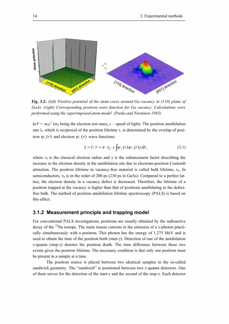
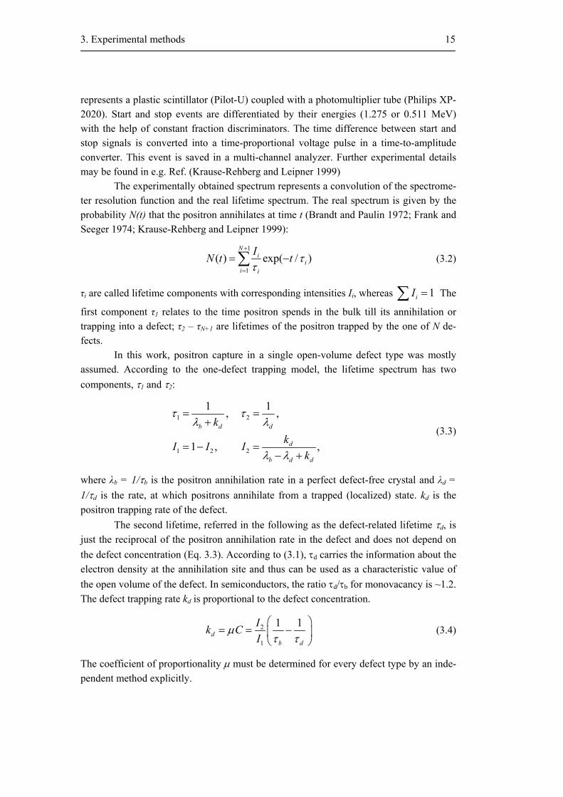
Positrons are unstable in matter. After its introduction into a material, the posi-trons life may be divided into three parts: thermalization, diffusion and annihilation. Thermalization represents a process of the energy loss of the positron via electron and phonon excitation. This process occurs very rapidly, during 3-4 ps (Puska and Nieminen 1994). Thereafter, the positron movement may be described as diffusion. In semiconduc-tors the diffusion constant is about 1.5-3 cm2s–1 (Soininen et al. 1992; Shan et al. 1997). In a defect-free material, the positron wave function is a delocalized Bloch wave exhibit-ing maxima in the interstitial region due to the Coulomb repulsion of the positively charged positron and atom cores (Fig. 3.1). In an imperfect crystal, however, the wave function of the positron may be localized at the sites, where an atom (or group of atoms) is missing, i.e. at the vacancies, vacancy complexes or other open-volume defects [Fig. 3.2 (right)]. The reason is that the absence of the core represents a potential well for the positron [Fig. 3.2 (left)]. Therefore, it is energetically favorable for the positron which has diffused to a vacancy to remain at the vacancy site. This process is called positron trap-ping.
The positron life is ended by annihilation with an electron. By the annihilation, the energy of the electron-positron pair (e–-e+) is converted into the annihilation γ-radiation. Mainly, there are two γ-photons emitted, each one having the energy of 511
Fig. 3.1: Positron wave function in defect-free GaAs. The calcula-tion was performed using the su-perimposed-atom (Puska and Nieminen 1983) method for (110) plane.
14 3. Experimental methods
keV = m0c2 (m0 being the electron rest mass, c – speed of light). The positron annihilation rate λ, which is reciprocal of the positron lifetime τ, is determined by the overlap of posi-tron ( )rψ + and electron ( )rψ − wave functions:
01/ ( ) ( ) ,r c r r drλ τ π ψ ψ γ+ −= = ⋅ ⋅ ∫ (3.1)
where r0 is the classical electron radius and γ is the enhancement factor describing the increase in the electron density at the annihilation site due to electrons-positron Coulomb attraction. The positron lifetime in vacancy-free material is called bulk lifetime, τb. In semiconductors, τb is in the order of 200 ps (230 ps in GaAs). Compared to a perfect lat-tice, the electron density in a vacancy defect is decreased. Therefore, the lifetime of a positron trapped at the vacancy is higher than that of positrons annihilating in the defect-free bulk. The method of positron annihilation lifetime spectroscopy (PALS) is based on this effect.
3.1.2 Measurement principle and trapping model For conventional PALS investigations, positrons are usually obtained by the radioactive decay of the 22Na isotope. The main reason consists in the emission of a γ-photon practi-cally simultaneously with a positron. This photon has the energy of 1.275 MeV and is used to obtain the time of the positron birth (start-γ). Detection of one of the annihilation γ-quanta (stop-γ) denotes the positron death. The time difference between these two events gives the positron lifetime. The necessary condition is that only one positron must be present in a sample at a time. The positron source is placed between two identical samples in the so-called sandwich geometry. The “sandwich” is positioned between two γ-quanta detectors. One of them serves for the detection of the start-γ and the second of the stop-γ. Each detector
Fig. 3.2: (left) Positive potential of the atom cores around Ga vacancy in (110) plane of GaAs. (right) Corresponding positron wave function for Ga vacancy. Calculations were performed using the superimposed-atom model (Puska and Nieminen 1983)
3. Experimental methods 15
represents a plastic scintillator (Pilot-U) coupled with a photomultiplier tube (Philips XP-2020). Start and stop events are differentiated by their energies (1.275 or 0.511 MeV) with the help of constant fraction discriminators. The time difference between start and stop signals is converted into a time-proportional voltage pulse in a time-to-amplitude converter. This event is saved in a multi-channel analyzer. Further experimental details may be found in e.g. Ref. (Krause-Rehberg and Leipner 1999) The experimentally obtained spectrum represents a convolution of the spectrome-ter resolution function and the real lifetime spectrum. The real spectrum is given by the probability N(t) that the positron annihilates at time t (Brandt and Paulin 1972; Frank and Seeger 1974; Krause-Rehberg and Leipner 1999):
1
1( ) exp( / )
Ni
ii i
IN t t ττ
+
=
= −∑ (3.2)
τi are called lifetime components with corresponding intensities Ii, whereas 1iI =∑ The
first component τ1 relates to the time positron spends in the bulk till its annihilation or trapping into a defect; τ2 – τN+1 are lifetimes of the positron trapped by the one of N de-fects. In this work, positron capture in a single open-volume defect type was mostly assumed. According to the one-defect trapping model, the lifetime spectrum has two components, τ1 and τ2:
1 2
1 2 2
1 1, ,
1 , ,
b d d
d
b d d
kkI I I
k
τ τλ λ
λ λ
= =+
= − =− +
(3.3)
where λb = 1/τb is the positron annihilation rate in a perfect defect-free crystal and λd = 1/τd is the rate, at which positrons annihilate from a trapped (localized) state. kd is the positron trapping rate of the defect. The second lifetime, referred in the following as the defect-related lifetime τd, is just the reciprocal of the positron annihilation rate in the defect and does not depend on the defect concentration (Eq. 3.3). According to (3.1), τd carries the information about the electron density at the annihilation site and thus can be used as a characteristic value of the open volume of the defect. In semiconductors, the ratio τd/τb for monovacancy is ~1.2. The defect trapping rate kd is proportional to the defect concentration.
2
1
1 1d
b d
Ik CI
µτ τ
= = −
(3.4)
The coefficient of proportionality µ must be determined for every defect type by an inde-pendent method explicitly.
16 3. Experimental methods
Very often, a parameter called average positron lifetime, τav is used in the litera-ture. This parameter is given as:
1
1
N
av i ii
Iτ τ+
=
= ∑ (3.5)
In principle, τav represents the centre of mass of the lifetime spectrum. Therefore, it is rather insensitive to the numerical fitting procedure applied. If bulk and defect-related lifetime are known, the trapping rate kd may be determined from the average lifetime as:
1 av bd
b d av
k τ ττ τ τ
−=
− (3.6)
3.2 Temperature dependence of positron trapping in semi-conductors
In contrast to metals, the trapping coefficient in semiconductors often reveals some tem-perature dependence, which might be different for different semiconductors or different defect types. A good example is given in section 7, where temperature dependent positron lifetime measurements in silicon- and tellurium-doped GaAs are discussed. Obviously, the temperature behavior of the trapping coefficient is specific for a certain defect and cares important information about defect properties. In order to be able to extract this in-formation, details of positron trapping and reasons of its temperature dependence must be understood. This section gives a short overview of the current state of knowledge of the positron capture mechanisms in semiconductors and their temperature dependence. Firstly, a short description of the theoretical model of positron trapping is given, with an emphasis placed on the calculation of the trapping coefficient as a function of tempera-ture. Secondly, I present the application of the model for fitting of the experimental re-sults.
3.2.1 Theory Most of the work on the theoretical description of positron trapping in semiconductors was done by a Finnish group (M. Puska, R. Nieminen et al.) in the late 80’s. They pro-vided calculations for two kinds of positron traps – vacancies in different charge states and negative ions. The trapping coefficient was obtained with the help of Fermi’s golden-rule formula:
( )2
,4 ,i f i f i fPP M E Eν π δ= −∑ (3.7)
3. Experimental methods 17
where Pi is the probability that the initial combined positron-host state i is occupied
and Pf the probability that the final state f is allowed. Mi,f is the matrix element of the
interaction potential, which takes into account the energy transfer during the positron transition from the initial Ei to final Ef state. The summation in (3.7) is taken over all pos-sible states meeting the energy conservation condition. Assuming the Maxwell-Boltzmann form for the initial positron distribution, the trapping coefficient as a function of temperature is given as the average:
3/ 2/
0
2( ) ( ) ,BE k T
B
mT dE E e Ek T
ν νπ
∞−+
=
∫ (3.8)
where kB is the Boltzmann constant and m+ the positron effective mass. In order to describe the interaction potential and to define the initial and final
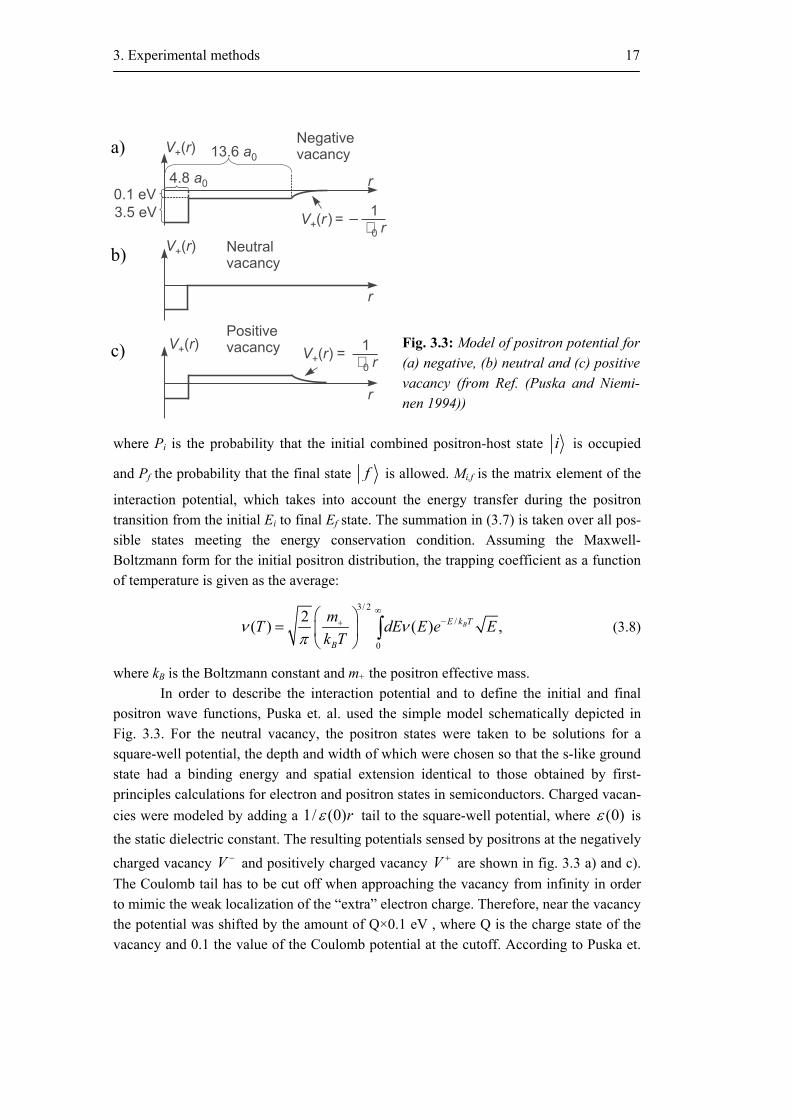
positron wave functions, Puska et. al. used the simple model schematically depicted in Fig. 3.3. For the neutral vacancy, the positron states were taken to be solutions for a square-well potential, the depth and width of which were chosen so that the s-like ground state had a binding energy and spatial extension identical to those obtained by first-principles calculations for electron and positron states in semiconductors. Charged vacan-cies were modeled by adding a 1/ (0)rε tail to the square-well potential, where (0)ε is the static dielectric constant. The resulting potentials sensed by positrons at the negatively charged vacancy V − and positively charged vacancy V + are shown in fig. 3.3 a) and c). The Coulomb tail has to be cut off when approaching the vacancy from infinity in order to mimic the weak localization of the “extra” electron charge. Therefore, near the vacancy the potential was shifted by the amount of Q×0.1 eV , where Q is the charge state of the vacancy and 0.1 the value of the Coulomb potential at the cutoff. According to Puska et.
0.1 eV
3.5 eV
V r+( )
V r+( )
V r+( )
13.6 a0
4.8 a0
Negativevacancy
Neutralvacancy
Positivevacancy
r
r
r
V r+( ) = �
1� 0 r
V r+( ) =1
� 0 r
Fig. 3.3: Model of positron potential for (a) negative, (b) neutral and (c) positive vacancy (from Ref. (Puska and Niemi-nen 1994))
a)
b)
c)

18 3. Experimental methods
al., this constant potential shift does not change the positron localization in the bound state and the energy value is simply shifted by the same amount as the potential. But the potential shift and the Coulomb tail can have a large effect on the delocalized positron wave functions at thermal energies, as demonstrated in the following. One of the main model assumptions is that the long-range Coulomb tail intro-duces several positron Rydbergs states with low binding energies. These states may act as precursor states in the trapping process and thereby enhance the overall trapping coeffi-cient for the defect. Thus, the trapping process of a delocalized positron may be divided into two parts: (i) direct trapping into the ground state at a vacancy and (ii) two-stage trapping – firstly, into a weakly localized Rydberg state from which the positron then makes a transition into a deeper localized state. Corresponding to these two kinds of posi-tron trapping, there are five possible energy-loss mechanisms, in which the energy of a delocalized positron is released: (i) Direct trapping: (a) electron-hole excitation from the valence to the conduction band; (b) electron-hole excitation from the localized defect-level to the conduction band; (ii) Two-stage trapping: (c) phonon-assisted capture of a delocalized positron into a Rydberg state; (d) phonon-assisted transitions between Rydberg states; (e) transition from a Rydberg state to the ground state. These processes are illustrated in Fig. 3.4.
Fig. 3.4: Schematic representation of the positron energy-loss mechanisms: (a) interband electron-hole excitations and (b) exciting of the electron from a defect level to conduction band; (c) trapping into Rydberg states; transition (d) between Rydberg states and (e) be-tween Rydberg and ground states. (From Ref. (Puska and Nieminen 1994))
3. Experimental methods 19
In fact, only the first three transition mechanisms relate to the capture of a delo-calized positron and thus determine the temperature dependence of the trapping coeffi-cient. The process most sensitive to temperature is positron trapping into a Rydberg state of shallow Coulomb potential of a negative vacancy. Since the binding energy of the positron to the trap is low, there is a certain probability of the escape (detrapping) of the positron from the trap back to a delocalized state. When the delocalized and the trapped states are in thermal equilibrium the detrapping rate δ and the trapping rate k at a given temperature are given as (Puska and Nieminen 1994):
3/ 2/
2
1 ,2
R BE k TB
v
m k T ek cδ
π−+ = h
(3.9)
where 2 3/ 2[ / 2 ]c BN m k T π+= h is the density of positron states per volume in the posi-
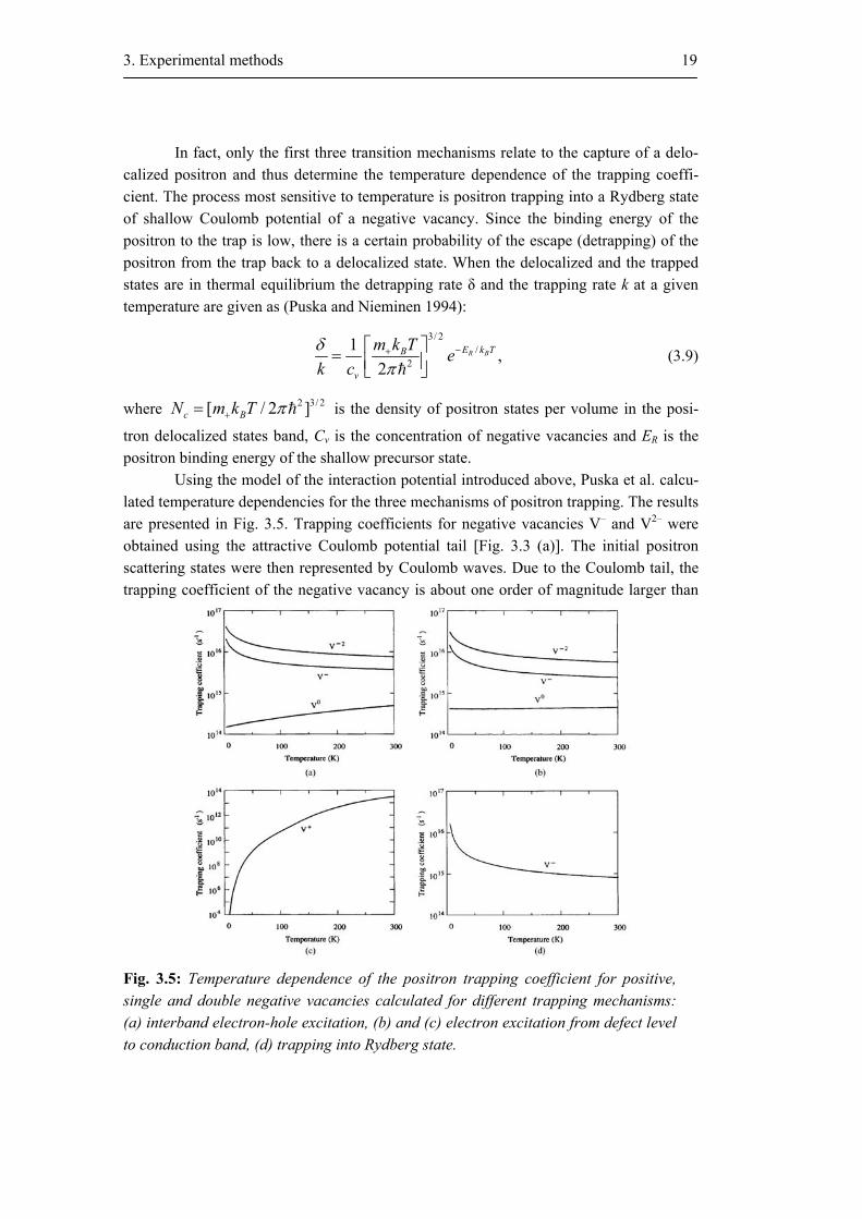
tron delocalized states band, Cv is the concentration of negative vacancies and ER is the positron binding energy of the shallow precursor state. Using the model of the interaction potential introduced above, Puska et al. calcu-lated temperature dependencies for the three mechanisms of positron trapping. The results are presented in Fig. 3.5. Trapping coefficients for negative vacancies V– and V2– were obtained using the attractive Coulomb potential tail [Fig. 3.3 (a)]. The initial positron scattering states were then represented by Coulomb waves. Due to the Coulomb tail, the trapping coefficient of the negative vacancy is about one order of magnitude larger than
Fig. 3.5: Temperature dependence of the positron trapping coefficient for positive, single and double negative vacancies calculated for different trapping mechanisms: (a) interband electron-hole excitation, (b) and (c) electron excitation from defect level to conduction band, (d) trapping into Rydberg state.

20 3. Experimental methods
the one of the neutral vacancy [Fig. 3.5 (a, b)]. At 300 K, it amounts to 2-5×10¹⁴ s–1 and 2-4×10¹⁵ s–1 for the neutral and singly negative vacancy, respectively. These values are in good agreement with the trapping coefficients found experimentally for the negatively charged gallium vacancy in GaAs (Le Berre et al. 1995; Gebauer et al. 1997). As Fig. 3.5 shows, the temperature coefficient for the neutral vacancy V0 is either independent of the temperature [Fig. 3.5 (b)] or increases by factor of 3 as temperature rises from 0 to 300 K [Fig. 3.5 (a)]. The increasing behavior is due to p-type scattering resonance for delocalized positron states at energies above the typical thermal energies. If the positron kinetic energy is near the resonance, the initial positron state is strongly en-hanced at the vacancy, what increases the overlap of the initial and final states and thus also the positron trapping coefficient. However, the p resonance is significant only for interband electron-hole excitation [Fig. 3.4 (a)], whereas it has a little effect on the trap-ping coefficient for the trapping process mediated by the excitation of electrons from lo-calized defect levels [Fig. 3.4 (b)]. For a more detailed explanation, the reader is refered to Ref. (Puska et al. 1990). For the negative vacancy V–, the trapping coefficient increases towards lower temperatures and diverges at low temperatures being proportional to T–1/2. This diver-gence is a direct consequence of the normalization of the initial positron wave function. The square of the amplitude of the Coulomb wave at the origin, i.e. at the center of the vacancy, is at maximum and behaves as (Mott and Massey 1965):
2, 2| (0) | ,
1i pue πα
α∝
− (3.10)
where
.m Qp
αε
+= (3.11)
The ε in Eq. (3.11) is the dielectric constant and p is the positron wave-vector. For a negative charge state Q, the square of the matrix element (3.7) and thus the positron trap-ping coefficient are inversely proportional to the square root of the positron energy. The integral over energy in Eq. (3.8) becomes then proportional to the temperature, what to-gether with the prefactor of T–3/2 gives the trapping coefficient proportional to T–1/2. For α close to zero, the amplitude in (3.10) approaches a constant value and the wave function becomes a plane wave. Thus, the trapping coefficient of neutral vacancies does not di-verge at low temperatures. For a double negative vacancy V2–, a similar temperature be-havior of the trapping coefficient was predicted. According to (3.10), the trapping coeffi-cient is directly proportional to Q and the ratio of the trapping coefficients for V2– and V– should be a factor of 2 [Fig. 3.5 (a, b)]. The temperature dependence of the trapping coefficient for a positively charged vacancy is plotted in Fig. 3.5 (c). As the calculations show, trapping into positively charged vacancies should be possible at temperatures higher than 200 K (ν ≥ 1013 s–1).

3. Experimental methods 21
However, this was never observed experimentally. The probable reason is that the posi-tron does not have enough time to tunnel through the repulsive Coulomb barrier. The result of the calculations for positron trapping into a Rydberg state of a nega-tive vacancy is shown in Fig. 3.5 (d). The trapping coefficient lies in the same order of magnitude as for the trapping into a ground state. However, it decreases more strongly with increasing temperature, because of detrapping of positrons from the Rydberg state due to the small binding energy (Eq. 3.9).
3.2.2 Model of positron trapping for experimental data fitting This section describes a model of positron trapping for fitting of τav(T) curves obtained experimentally. The average positron lifetime is chosen for fitting, since it is a most sta-ble and thus reliable parameter in the procedure of spectra analysis, which does not de-pend much on the details of decomposition. At the heart of the model, the theoretical con-siderations of two-stage positron trapping presented in the previous section are lying. Two cases of positron trapping are considered: 1) one-defect model: positron trapping by negative vacancies only; 2) two-defect model: positron trapping by negative vacancies and negative ions (shallow traps). 1) One-defect model: negative vacancies. For positron trapping at a single defect, the trapping rate is given by Eq. 3.6. After a sim-ple algebraic transformation, the average positron lifetime can be expressed as:
1 .1
d vav b
d b
KK
ττ ττ
+=
+ (3.12)
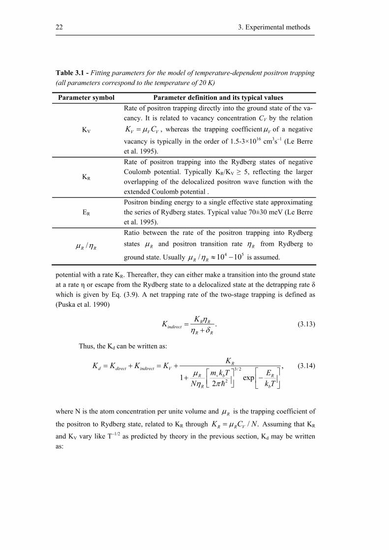
According to the two-stage trapping model (Fig. 3.6), the global trapping rate Kd is given by the sum of two trapping mechanisms: direct and indirect two-stage trapping. The di-rect trapping to the ground state of the vacancy occurs at a rate KV. In the two-stage trap-ping model, positrons are captured into the Rydberg states of the long-range Coulomb
Fig. 3.6: Model of positron trapping into negative vacancy involving positron capture into Rydberg states of the attractive Coulomb potential at rate KR and positron detrapping from these states at rate δR.
22 3. Experimental methods
potential with a rate KR. Thereafter, they can either make a transition into the ground state at a rate η or escape from the Rydberg state to a delocalized state at the detrapping rate δ which is given by Eq. (3.9). A net trapping rate of the two-stage trapping is defined as (Puska et al. 1990)
.R Rindirect
R R
KK ηη δ
=+
(3.13)
Thus, the Kd can be written as:
3/ 2
2
,1 exp
2
Rd direct indirect V
bR R
R b
KK K K Km k T E
N k Tµη π
+
= + = + + − h
(3.14)
where N is the atom concentration per unite volume and Rµ is the trapping coefficient of
the positron to Rydberg state, related to KR through / .R R VK C Nµ= Assuming that KR
and KV vary like T–1/2 as predicted by theory in the previous section, Kd may be written as:
Table 3.1 - Fitting parameters for the model of temperature-dependent positron trapping (all parameters correspond to the temperature of 20 K)
Parameter symbol Parameter definition and its typical values
KV
Rate of positron trapping directly into the ground state of the va-cancy. It is related to vacancy concentration CV by the relation
V V VK Cµ= , whereas the trapping coefficient Vµ of a negative
vacancy is typically in the order of 1.5-3×1016 cm3s–1 (Le Berre et al. 1995).
KR
Rate of positron trapping into the Rydberg states of negative Coulomb potential. Typically KR/KV ≥ 5, reflecting the larger overlapping of the delocalized positron wave function with the extended Coulomb potential .
ER Positron binding energy to a single effective state approximating the series of Rydberg states. Typical value 70±30 meV (Le Berre et al. 1995).
/R Rµ η
Ratio between the rate of the positron trapping into Rydberg states Rµ and positron transition rate Rη from Rydberg to
ground state. Usually 4 5/ 10 10R Rµ η ≈ − is assumed.
3. Experimental methods 23
1/ 2
1/ 2
1/ 2 3/ 2
2
(20 )20
(20 ) .20
1 exp20 2
R
d V
bR R
R b
TK KKTK K K
K m k TT EN K k Tµη π
−
−
−
+
= +
+ − h
(3.15)
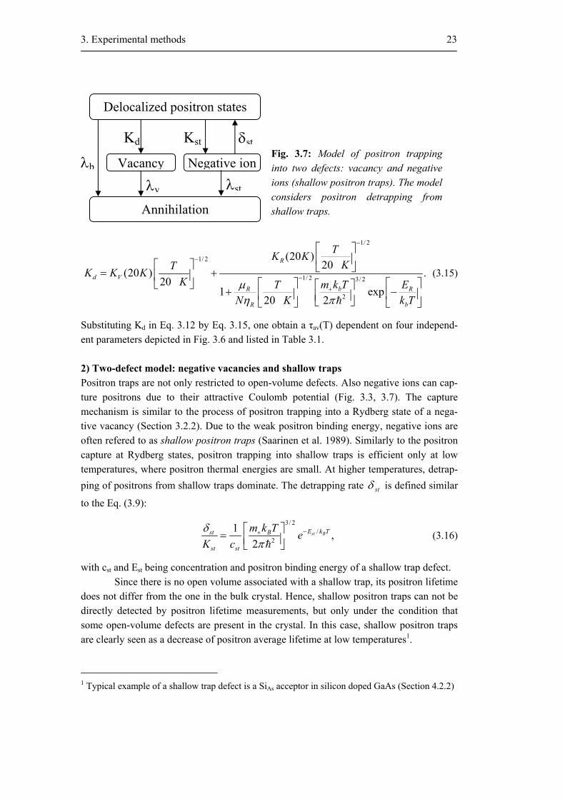
Substituting Kd in Eq. 3.12 by Eq. 3.15, one obtain a τav(T) dependent on four independ-ent parameters depicted in Fig. 3.6 and listed in Table 3.1. 2) Two-defect model: negative vacancies and shallow traps Positron traps are not only restricted to open-volume defects. Also negative ions can cap-ture positrons due to their attractive Coulomb potential (Fig. 3.3, 3.7). The capture mechanism is similar to the process of positron trapping into a Rydberg state of a nega-tive vacancy (Section 3.2.2). Due to the weak positron binding energy, negative ions are often refered to as shallow positron traps (Saarinen et al. 1989). Similarly to the positron capture at Rydberg states, positron trapping into shallow traps is efficient only at low temperatures, where positron thermal energies are small. At higher temperatures, detrap-ping of positrons from shallow traps dominate. The detrapping rate stδ is defined similar
to the Eq. (3.9):
3/ 2/
2
1 ,2
st BE k Tst B
st st
m k T eK cδ
π−+ = h
(3.16)
with cst and Est being concentration and positron binding energy of a shallow trap defect. Since there is no open volume associated with a shallow trap, its positron lifetime
does not differ from the one in the bulk crystal. Hence, shallow positron traps can not be directly detected by positron lifetime measurements, but only under the condition that some open-volume defects are present in the crystal. In this case, shallow positron traps are clearly seen as a decrease of positron average lifetime at low temperatures1.
1 Typical example of a shallow trap defect is a SiAs acceptor in silicon doped GaAs (Section 4.2.2)
Delocalized positron states
Vacancy Negative ion
Kd Kst δst
Annihilation
λstλv
λbFig. 3.7: Model of positron trapping into two defects: vacancy and negative ions (shallow positron traps). The model considers positron detrapping from shallow traps.
24 3. Experimental methods
Thus, when shallow positron traps are present in the crystal, the one-defect trap-ping model described above is only applicable at temperatures higher than 200 K. At lower temperatures, positrons are trapped into both vacancy and shallow trap defects and thus the two-defect trapping model must be used. The average positron lifetime can be written as (Le Berre et al. 1995):
( ),
( )
st std d d
st stav d
st stb d st
st st
KK K
KK K
λ δλ λτ τ
λ δλ λ
+ + +
=
+ + +
(3.17)
where λd = 1/τd is the annihilation rate at the vacancy defect and λst = λb = 1/τb are the an-nihilation rates at the shallow trap defect and in the bulk, respectively. The ratio /st stKδ
of the detrapping rate to the trapping rate at the shallow traps is determined by Eq. (1.11). Similar to the Kd, it is assumed that Kst varies like T–1/2. At very low temperatures, the positrons thermal detrapping from the shallow traps may be neglected in first approximation. Kst(20K) is then calculated using a simple two-defect trapping model:
(20 ) (20 )(20 ) (20 )(20 ) (20 )
av b av dst b d
st av av st
K KK K K KK K
τ τ τ τλτ τ τ τ
− −= −
− −, (3.18)
where τst is assumed to be equal to τb. This formula is useful, if Kd(300K) can be deter-mined from high-temperature measurements using a one-defect model. Kd(20K) can be then calculated from Kd(300K) using the temperature dependence K(T) ~ T–1/2 (Le Berre et al. 1995).
3.3 Coincidence Doppler-broadening spectroscopy
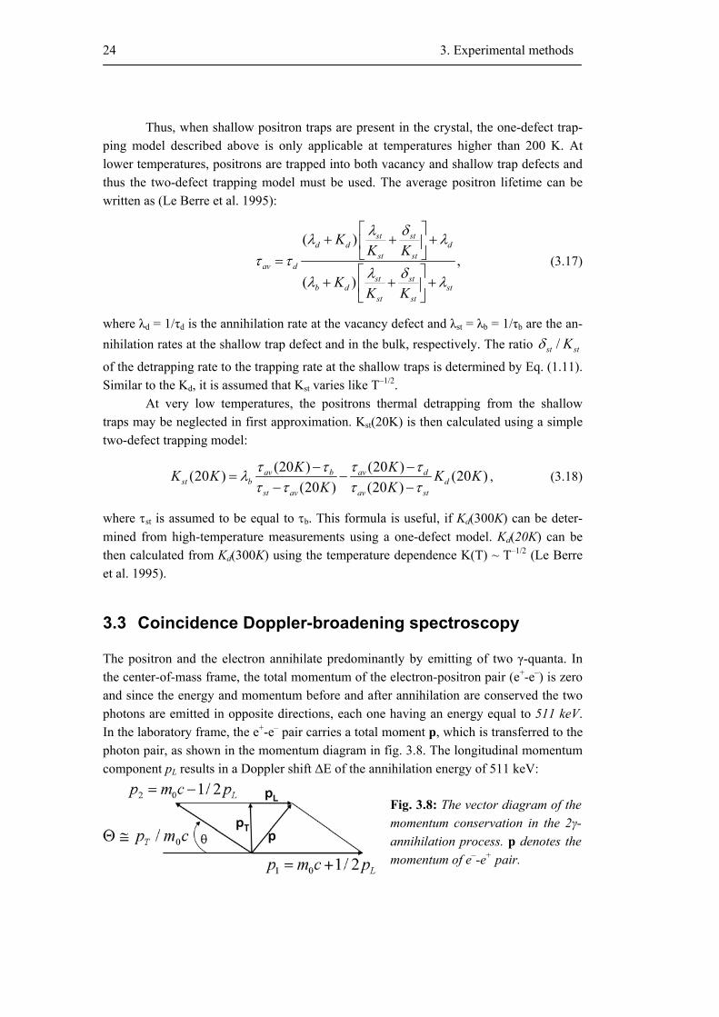
The positron and the electron annihilate predominantly by emitting of two γ-quanta. In the center-of-mass frame, the total momentum of the electron-positron pair (e+-e–) is zero and since the energy and momentum before and after annihilation are conserved the two photons are emitted in opposite directions, each one having an energy equal to 511 keV. In the laboratory frame, the e+-e– pair carries a total moment p, which is transferred to the photon pair, as shown in the momentum diagram in fig. 3.8. The longitudinal momentum component pL results in a Doppler shift ∆E of the annihilation energy of 511 keV:
Fig. 3.8: The vector diagram of the momentum conservation in the 2γ-annihilation process. p denotes the momentum of e–-e+ pair.
3. Experimental methods 25
/ 2LE p c∆ = (3.18)
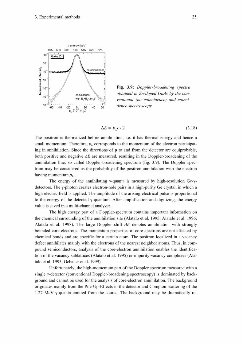
The positron is thermalized before annihilation, i.e. it has thermal energy and hence a small momentum. Therefore, pL corresponds to the momentum of the electron participat-ing in annihilation. Since the directions of p to and from the detector are equiprobable, both positive and negative ∆E are measured, resulting in the Doppler-broadening of the annihilation line, so called Doppler-broadening spectrum (fig. 3.9). The Doppler spec-trum may be considered as the probability of the positron annihilation with the electron having momentum pL. The energy of the annihilating γ-quanta is measured by high-resolution Ge-γ-detectors. The γ-photon creates electron-hole pairs in a high-purity Ge crystal, in which a high electric field is applied. The amplitude of the arising electrical pulse is proportional to the energy of the detected γ-quantum. After amplification and digitizing, the energy value is saved in a multi-channel analyzer. The high energy part of a Doppler-spectrum contains important information on the chemical surrounding of the annihilation site (Alatalo et al. 1995; Alatalo et al. 1996; Alatalo et al. 1998). The large Doppler shift ∆E denotes annihilation with strongly bounded core electrons. The momentum properties of core electrons are not affected by chemical bonds and are specific for a certain atom. The positron localized in a vacancy defect annihilates mainly with the electrons of the nearest neighbor atoms. Thus, in com-pound semiconductors, analysis of the core-electron annihilation enables the identifica-tion of the vacancy sublattices (Alatalo et al. 1995) or impurity-vacancy complexes (Ala-talo et al. 1995; Gebauer et al. 1999).
Unfortunately, the high-momentum part of the Doppler spectrum measured with a single γ-detector (conventional Doppler-broadening spectroscopy) is dominated by back-ground and cannot be used for the analysis of core-electron annihilation. The background originates mainly from the Pile-Up-Effects in the detector and Compton scattering of the 1.27 MeV γ-quanta emitted from the source. The background may be dramatically re-
495 500 505 510 515 520 525
10-6
10-5
10-4
10-3
10-2
10-1
100
coincidencewith E1+E2=2m0c
2
no coincidence
γ energy (keV)
GaAs:Zn
Nor
mal
ized
inte
nsity
-60 -40 -20 0 20 40 60 pL (10-3 m0c)
Fig. 3.9: Doppler-broadening spectra obtained in Zn-doped GaAs by the con-ventional (no coincidence) and coinci-dence spectroscopy.
26 3. Experimental methods
duced by the coincident registrations of both γ-quanta with the help of two detectors (Lynn et al. 1977; MacDonald et al. 1978; Troev et al. 1979). This technique received the name Coincidence Doppler-broadening Spectroscopy (CDBS). Using CDBS, the back-ground may be suppressed by at least two orders of magnitude (fig. 3.9). The detailed description of the procedure to obtain the coincidence spectrum is given in Ref. (Gebauer et al. 1999).
The most important parameter sensitive to the chemical surrounding of the anni-hilation site is the form of the high-momentum distribution (Myler et al. 1996; Myler and Simpson 1997). In order to make the analysis of the spectrum form easier, so called ratio curves were introduced (Myler et al. 1996; Szpala et al. 1996). The ratio-curves are ob-tained by dividing the measured spectra by a reference one. As a reference, a spectrum of defect-free samples is usually taken. Often, CDB-measurements are performed in a pure elemental material as a reference in order to obtain a spectrum specific for the chemical element of interest. The characteristic features of the high-momentum part of the spec-trum are conserved also in different environments. This provides a possibility to deduce whether the detected vacancy is neighbored by a certain atom (e.g. Cu in GaAs, fig. 5.11).
3.4 Procedure of positron annihilation measurements
The present study is based predominantly on the results of temperature-dependent meas-urement of positron annihilation lifetime. Three conventional fast-fast coincidence sys-tems with resolution of 225 ps, 240 ps and 250 ps were at the experimentalist’s disposal. A small quantity of radioactive Na22-salt covered with 1.5 µm Al-foil was used as a posi-tron source, which was placed in sandwich geometry between two identical samples. Typical source activity amounted to 1-1.5 MBq. The measurement temperature, Tmeas, could be varied in the 20 K – 600 K range. Usually, the temperature program of lifetime experiments consisted of alternating temperatures. This means that Tmeas was changed always with a step of 2×Tstep from 300 K (room temperature) to the lowest temperature, then to the highest one and finally back to the room temperature, where Tstep is a tempera-ture step between two measurement temperatures. So, by Tstep of 33 K used in this work most often, the temperature program will include following temperatures: 300 K, 234 K, 168 K, 102 K, 36 K, 20 K, 69 K, 135 K, 201 K, 267 K, 333 K, 399 K, 465 K, 498 K, 432, 366 K, 300 K. Such kind of measurement program is used to recognize a temperature-related hysteresis, if such takes place.
In each lifetime spectrum, 3 to 5 ×10⁶ annihilation events were accumulated. The spectra were analyzed with the help of “Lifspecfit” routine (Puska 1978) after source and background correction. A piece of p-type Zn-doped or SI undoped GaAs exhibiting no positron trapping was used as a reference. In the source correction procedure, three life-time components were assumed corresponding to annihilation inside the NaCl source ( NaCτ ) or the covering aluminum foil ( Alτ ) and to three-photon annihilation from posi-

3. Experimental methods 27
tronium state ( psτ ). The source correction was performed by the analysis of the reference
lifetime spectrum. The lifetime intensities and psτ were used as fitting parameters,
whereas NaCτ and Alτ were fixed to 380 ps and 165 ps, respectively (Somieski et al.
1996). The source parameters were considered as determined, when the positron lifetime of 230 ps, the bulk lifetime in GaAs (Gebauer et al. 2000), was obtained. Typically, source contribution did not exceed 15%, where the positronium share was in the order of 1%.
Doppler broadening coincidence spectroscopy was carried out using two Ge-γ-detectors with a channel width of 70.60 eV and an energy resolution of 0.9 keV. In each Doppler spectrum, about 5×10⁷ coincident events during 5-6 days were collected. The intensity of the annihilation with high-momentum core electrons was characterized by the W parameter, defined as the relative intensity in the momentum range (10-20)×10-3 m0c, where m0c is the electron rest energy. For a qualitative analysis, the CDB curves were always normalized to the data obtained in SI undoped GaAs used as reference.
3.5 Other methods
Except the methods of positron annihilation, several additional methods were applied for the characterization of the GaAs crystals investigated in this work: Photo- and cathodoluminescence (PL and CL) spectroscopy Both of these techniques are contactless, nondestructive methods of probing the elec-tronic structure of materials. Their basic principle involves the excitation of electrons from their ground state in the valence band to the conduction band or to some excited state within the band-gap associated with the defect energy level. When these electrons return to their equilibrium states, the excess energy is released and may include the emis-sion of light (a radiative process or luminescence) or may not (a nonradiative process). The excitation is performed either by high-energy photon (photoluminescence) or elec-trons (cathodoluminescence). The energy of the emitted light is related to the difference in energy levels between the two electron states involved in the transition. Thus, lumines-cence spectroscopy can provide important information about the energy level of the point defects present in the semiconductor. For further details see e.g. (Yacobi and Holt 1990). Measurements of the Hall Effect This is a well-known method for the determination of the type, concentration and mobil-ity of the free charge carriers in semiconductors. By the temperature-dependent Hall-measurements (TDH), it is possible to find out the activation energy of the dominating donor (acceptor) defect (Blakemore 1962).
28 3. Experimental methods
Secondary Ion and Glow Discharge Mass Spectrometry (SIMS and GDMS) SIMS and GDSM are destructive techniques for the analysis of the chemical compositeon of the inorganic solids. In this work, SIMS and GDMS were applied to obtain the concen-trations of impurity atoms in the GaAs crystals. The principle of these techniques in-volves the mass spectrometry analysis of the individual atoms obtained by means of sput-tering the sample surface by a primary energetic ion beam (SIMS) by sputtering of the sample in low-pressure DC plasma. For further explanations see e.g. (Feldman and Mayer 1986).