2n5486
DESCRIPTION
Data SheetTRANSCRIPT

2N5484 / 2N
5485 / 2N5486 / M
MB
F5484 / M
MB
F5485 / M
MB
F5486
2N54842N54852N5486
MMBF5484MMBF5485MMBF5486
N-Channel RF Amplifier
This device is designed primarily for electronic switchingapplications such as low On Resistance analog switching.Sourced from Process 50.
Absolute Maximum Ratings* TA = 25°C unless otherwise noted
Symbol Parameter Value UnitsVDG Drain-Gate Voltage 25 V
VGS Gate-Source Voltage - 25 V
IGF Forward Gate Current 10 mA
TJ ,Tstg Operating and Storage Junction Temperature Range -55 to +150 °C
GS D
TO-92SOT-23
Mark: 6B / 6M / 6H
G
S
D
*These ratings are limiting values above which the serviceability of any semiconductor device may be impaired.
NOTES:1) These ratings are based on a maximum junction temperature of 150 degrees C.2) These are steady state limits. The factory should be consulted on applications involving pulsed or low duty cycle operations.
Thermal Characteristics TA = 25°C unless otherwise noted
Symbol Characteristic Max Units2N5484 *MMBF5484
PD Total Device DissipationDerate above 25°C
3502.8
2251.8
mWmW/°C
RθJC Thermal Resistance, Junction to Case 125 °C/W
RθJA Thermal Resistance, Junction to Ambient 357 556 °C/W
*Device mounted on FR-4 PCB 1.6" X 1.6" X 0.06."
Discrete POWER & SignalTechnologies
ã 1997 Fairchild Semiconductor Corporation

2N5484 / 2N
5485 / 2N5486 / M
MB
F5484 / M
MB
F5485 / M
MB
F5486
Electrical Characteristics TA = 25°C unless otherwise noted
OFF CHARACTERISTICS
Symbol Parameter Test C onditions Min Typ Max Units
ON CHARACTERISTICS
V(BR)GSS Gate-Source Breakdown Voltage IG = - 1.0 µA, VDS = 0 - 25 V
IGSS Gate Reverse Current VGS = - 20 V, VDS = 0VGS = - 20 V, VDS = 0, TA = 100°C
- 1.0- 0.2
nAµA
VGS(off) Gate-Source Cutoff Voltage VDS = 15 V, ID = 10 nA 2N54842N54852N5486
- 0.3- 0.5- 2.0
- 3.0- 4.0- 6.0
VVV
IDSS Zero-Gate Voltage Drain Current* VDS = 15 V, VGS = 0 2N54842N54852N5486
1.04.08.0
5.01020
mAmAmA
SMALL SIGNAL CHARACTERISTICSgfs Forward Transfer Conductance VDS = 15, VGS = 0, f = 1.0 kHz
2N54842N54852N5486
300035004000
600070008000
µmhosµmhosµmhos
Re(yis) Input Conductance VDS = 15, VGS = 0, f = 100 MHz2N5484
VDS = 15, VGS = 0, f = 400 MHz2N5485 / 2N5486
100
1000
µmhos
µmhosgos Output Conductance VDS = 15, VGS = 0, f = 1.0 kHz
2N54842N54852N5486
506075
µmhosµmhosµmhos
Re(yos) Output Conductance VDS = 15, VGS = 0, f = 100 MHz2N5484
VDS = 15, VGS = 0, f = 400 MHz2N5485 / 2N5486
75
100
µmhos
µmhosRe(yfs) Forward Transconductance VDS = 15, VGS = 0, f = 100 MHz
2N5484VDS = 15, VGS = 0, f = 400 MHz
2N54852N5486
2500
30003500
µmhos
µmhosµmhos
Ciss Input Capacitance VDS = 15, VGS = 0, f = 1.0 MHz 5.0 pF
Crss Reverse Transfer Capacitance VDS = 15, VGS = 0, f = 1.0 MHz 1.0 pF
Coss Output Capacitance VDS = 15, VGS = 0, f = 1.0 MHz 2.0 pF
NF Noise Figure VDS= 15 V, RG = 1.0 kΩ, f = 100 MHz 2N5484VDS= 15 V, RG = 1.0 kΩ, f = 400 MHz 2N5484VDS= 15 V , RG = 1.0 kΩ, f = 100 MHz 2N5485 / 2N5486VDS= 15 V, RG = 1.0 kΩ, f = 400 MHz 2N5485 / 2N5486
4.0
3.0
2.0
4.0
dB
dB
dB
dB
*Pulse Test: Pulse Width £ 300 ms, Duty Cycle £ 2%
N-Channel RF Amplifier(continued)
2N5484 / 2N
5485 / 2N5486 / M
MB
F5484 / M
MB
F5485 / M
MB
F5486
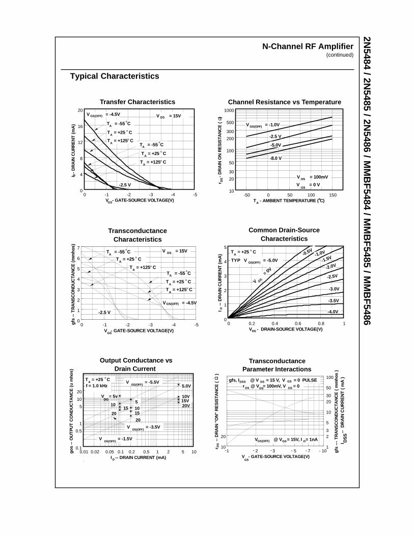
Typical Characteristics
°°°°°
Transfer Characteristics
-5-4-3-2-100
4
8
12
16
20
V - GATE-SOURCE VOLTAGE(V)
I -
DR
AIN
CU
RR
EN
T (
mA
)D
GS(OFF)V = -4.5V V = 15VDS
T = +25 CA
O
-2.5 V
T = -55 CO
A
T = +125 CA
O
T = -55 CO
A
T = +25 CA
O
T = +125 CA
O
GS
Channel Resistance vs Temperature
-50 0 50 100 15010
20
30
50
100
200
300
500
1000
T - AMBIENT TEMPERATURE ( C)
r
- D
RA
IN O
N R
ES
ISTA
NC
E (
)Ω
V = -1.0VGS(OFF)
-2.5 V
-5.0V
-8.0 V
V = 100mVDS
V = 0 VGS
DS
A
TransconductanceCharacteristics
-5-4-3-2-100
1
2
3
4
5
6
7
V - GATE-SOURCE VOLTAGE(V)
gfs
-- T
RA
NS
CO
ND
UC
TAN
CE
(m
mho
s)
V = -4.5VGS(OFF)
V = 15VDS
T = +25 CA
O
-2.5 V
T = -55 CO
A
T = +125 CA
O
T = -55 CO
A
T = +25 CA
O
T = +125 CA
O
GS
Common Drain-SourceCharacteristics
0 0.2 0.4 0.6 0.8 10
1
2
3
4
5
V - DRAIN-SOURCE VOLTAGE(V)
I -
- D
RA
IN C
UR
RE
NT
(m
A)
V
= 0V
GS-2.5V
DS
-0.5V
-4.0V
-2.0V
-1.0V
-3.5V
-3.0V
-1.5VT = +25 C
AO
TYP V = -5.0VGS(OFF)
D
TransconductanceParameter Interactions
1 2 3 5 7 1010
20
1
23
5
10
2030
50
100
V - GATE-SOURCE VOLTAGE(V)
r
--
DR
AIN
"O
N"
RE
SIS
TAN
CE
(
)
gfs
---
TR
AN
SC
ON
DU
CTA
NC
E (
mm
hos
)
GS
I
--
DR
AIN
CU
RR
EN
T (
mA
)D
SS
DS
Ω gfs, I @ V = 15 V, V = 0 PULSEGSDSDSS
r @ V = 100mV, V = 0GSDSDS
V @ V = 15V, I = 1nAGS(OFF) GS D
- -----
Output Conductance vsDrain Current
0.01 0.02 0.05 0.1 0.2 0.5 1 2 5 100.1
0.5
1
5
10
20
I -- DRAIN CURRENT (mA)
gos
-- O
UT
PU
T C
ON
DU
CTA
NC
E (
u m
hos)
D
1510
T = +25 CA
O
f = 1.0 kHz
15105
20
15V10V
5.0V
20V
20
V = 5vDG
V = -5.5VGS(OFF)
V = -3.5VGS(OFF)
V = -1.5VGS(OFF)
N-Channel RF Amplifier(continued)

2N5484 / 2N
5485 / 2N5486 / M
MB
F5484 / M
MB
F5485 / M
MB
F5486
Power Dissipation vsAmbient Temperature
0 25 50 75 100 125 1500
50
100
150
200
250
300
350
TEMPERATURE ( C)
P
- P
OW
ER
DIS
SIP
ATIO
N (
mW
)D
o
Transconductance vsDrain Current
0.01 0.02 0.05 0.1 0.2 0.5 1 2 5 100.1
0.5
1
5
10
I - DRAIN CURRENT (mA)
gfs
-- T
RA
NS
CO
ND
UC
TAN
CE
(m
mho
s)
D
GSV = - 5VGS(OFF)
GSV = - 1.5VGS(OFF)
T = -55 CO
A
T = +25 CA
O
T = +125 CA
O
T = -55 CO
A
T = +25 CA
O
T = +125 CA
O
V = 15V
f = 1.0 kHz
DG
Noise Voltage vs Frequency
0.01 0.03 0.1 0.3 1 3 10 30 1001
5
10
f -- FREQUENCY (kHz)
e -
NO
ISE
VO
LTA
GE
( n
V/
Hz
)
V = 15VDG
BW = 6.0 Hz @ f = 10 Hz, 100 Hz = 0.2 f @ f > 1.0 kHz
I = 0.5 mAD
I = 3 mADn
Capacitance vs Voltage
-20-15-10-50
1
5
10
V -- GATE-SOURCE VOLTAGE(V)
C
( C
) --
CA
PAC
ITA
NC
E (p
F)
GS
isrs
C ( V = 0 V)
C ( V = 15 V)C ( V = 15 V)DS
DS
is
rs
f = 0.1 - 1.0 MHz
Noise Figure Frequency
10 20 30 50 100 200 300 500 10000
1
2
3
4
5
f -- FREQUENCY (MHz)
NF
--
NO
ISE
FIG
UR
E (
dB)
V = 15VDS
I = 5.0 mA
R = 1.0 k T = +25 C
AO
Ω
D
g
N-Channel RF Amplifier(continued)
SOT-23 TO-92
Typical Characteristics (continued)

2N5484 / 2N
5485 / 2N5486 / M
MB
F5484 / M
MB
F5485 / M
MB
F5486
Common Source Characteristics
Input Admittance
100 200 300 500 700 1000
1
5
10
f -- FREQUENCY (MHz)
Y
--
INP
UT
AD
MIT
TAN
CE
(m
mho
s) V = 15VV = 0GS
DS
(CS)
g iss
iss
b iss
Output Admittance
100 200 300 500 700 1000
1
f -- FREQUENCY (MHz)
Y
--
OU
TP
UT
CO
ND
UC
TAN
CE
(m
mho
s)
V = 15VV = 0GS
DS
(CS)
OS
S
b (x 10)OSS
gOSS
Forward Transadmittance
100 200 300 500 700 1000
1
5
10
f -- FREQUENCY (MHz)
Y
--
FO
RW
AR
D T
RA
NS
FE
R (
mm
hos)
V = 15VV = 0GS
DS
(CS)
-b fss
fss
+gfss
Reverse Transadmittance
100 200 300 500 700 1000
1
5
10
f -- FREQUENCY (MHz)
Y
--
RE
VE
RS
E T
RA
NS
FE
R (
mm
hos)
rss
V = 15VV = 0GS
DS
(CS)
- b
-g ( X 0.1)rss
rss
N-Channel RF Amplifier(continued)

2N5484 / 2N
5485 / 2N5486 / M
MB
F5484 / M
MB
F5485 / M
MB
F5486
Common Gate Characteristics
N-Channel RF Amplifier(continued)
Input Admittance
100 200 300 500 700 10001
5
10
f -- FREQUENCY (MHz)
Y
--
INP
UT
AD
MIT
TAN
CE
(m
mho
s) V = 15VV = 0GS
DS
(CG)
g igs
igs
b igs
Forward Transadmittance
100 200 300 500 700 1000
1
5
10
f -- FREQUENCY (MHz)
Y
--
FO
RW
AR
D T
RA
NS
FE
R (
mm
hos)
V = 15VV = 0GS
DS
(CG)
-b fgs
fgs
+gfgs
Reverse Transadmittance
100 200 300 500 700 1000
1
f -- FREQUENCY (MHz)
Y
--
RE
VE
RS
E T
RA
NS
FE
R (
mm
hos)
rgs
V = 15VV = 0GS
DS
(CG) grgs
- b rgs
Output Admittance
100 200 300 500 700 1000
1
f -- FREQUENCY (MHz)
Y
--
OU
TP
UT
CO
ND
UC
TAN
CE
(m
mho
s)
V = 15VV = 0GS
DS
(CG)
ogs
b (x 10)OgS
gOgs

TRADEMARKS
ACEx™CoolFET™CROSSVOLT™E2CMOSTM
FACT™FACT Quiet Series™FAST®
FASTr™GTO™HiSeC™
The following are registered and unregistered trademarks Fairchild Semiconductor owns or is authorized to use and isnot intended to be an exhaustive list of all such trademarks.
LIFE SUPPORT POLICY
FAIRCHILD’S PRODUCTS ARE NOT AUTHORIZED FOR USE AS CRITICAL COMPONENTS IN LIFE SUPPORTDEVICES OR SYSTEMS WITHOUT THE EXPRESS WRITTEN APPROVAL OF FAIRCHILD SEMICONDUCTOR CORPORATION.As used herein:
ISOPLANAR™MICROWIRE™POP™PowerTrench™QS™Quiet Series™SuperSOT™-3SuperSOT™-6SuperSOT™-8TinyLogic™
1. Life support devices or systems are devices orsystems which, (a) are intended for surgical implant intothe body, or (b) support or sustain life, or (c) whosefailure to perform when properly used in accordancewith instructions for use provided in the labeling, can bereasonably expected to result in significant injury to theuser.
2. A critical component is any component of a lifesupport device or system whose failure to perform canbe reasonably expected to cause the failure of the lifesupport device or system, or to affect its safety oreffectiveness.
PRODUCT STATUS DEFINITIONS
Definition of Terms
Datasheet Identification Product Status Definition
Advance Information
Preliminary
No Identification Needed
Obsolete
This datasheet contains the design specifications forproduct development. Specifications may change inany manner without notice.
This datasheet contains preliminary data, andsupplementary data will be published at a later date.Fairchild Semiconductor reserves the right to makechanges at any time without notice in order to improvedesign.
This datasheet contains final specifications. FairchildSemiconductor reserves the right to make changes atany time without notice in order to improve design.
This datasheet contains specifications on a productthat has been discontinued by Fairchild semiconductor.The datasheet is printed for reference information only.
Formative orIn Design
First Production
Full Production
Not In Production
DISCLAIMER
FAIRCHILD SEMICONDUCTOR RESERVES THE RIGHT TO MAKE CHANGES WITHOUT FURTHERNOTICE TO ANY PRODUCTS HEREIN TO IMPROVE RELIABILITY, FUNCTION OR DESIGN. FAIRCHILDDOES NOT ASSUME ANY LIABILITY ARISING OUT OF THE APPLICATION OR USE OF ANY PRODUCTOR CIRCUIT DESCRIBED HEREIN; NEITHER DOES IT CONVEY ANY LICENSE UNDER ITS PATENTRIGHTS, NOR THE RIGHTS OF OTHERS.