2.8-ghz prescaler keeps cost down.pdf
TRANSCRIPT

8/10/2019 2.8-GHz prescaler keeps cost down.pdf
http://slidepdf.com/reader/full/28-ghz-prescaler-keeps-cost-downpdf 1/14
The popularity and easy access of RS-232 ports lendthem to many com-
munication projects. You
can use a port “as is”or as a tiny parallel port when the exchangeuses only control lines. Beforethe asynchronous serial-datatransfer between two devices cantake place,you must ensure thatboth devices are configured tothe same data format and trans-mission rate. Usually, the OSutility or application programon the host computer performsthis task,which the OS or a com-bination of switches selects in
the peripheral.The design in Figure 1 and theaccompanying software realizethe requirement of automatical-ly equalizing the speed of theparties by adapting the bit rate of a C’s serial port to that of ahost computer. The host sends a knownASCII code to a C that estimates the bitrate of the transmission.The C samplesthe receiving end of a transmission line.As soon as the line goes low, indicating astart bit,the C clears the timer.After the
line again goes high, the C reads thetimer’s value and uses this value to cal-culate the bit rate of a transmission. The
C uses the calculated bit rate in a tim-ing-delay loop for clocking out the datafrom the C to the host computer dur-
ing transmission and for sampling the in-coming data during receiving mode.Thetime between those falling and risingedges on a transmission line depends, of course, on the transmitted ASCII symbol.Its good practice to use a symbol with2k 1 zeros on the low side. Then, when you include the start bit, there are 2 k trail-ing zeroes. One timing unit is easier toderive by substituting a division with k right shifts.
The application in Figure 1 uses an 8-bit RISC P and an ASCII code of 8 (38hex) to establish a serial communication.Any symbol that ends with 8H also
works. The timer increments its valueevery 4P/FOSC seconds, where P is aprescaler factor and F OSC is the P’s clock frequency. Thus, the timer’s value after 4bits have transmitted during the time be-tween the falling and rising edge, is
T 4/BR, is N FOSC/(BR P), where BR is the bit rate.
Now you can derive the 1-bit trans-mission time, which is a reciprocal of atransmission speed, as (N/4)(4P)/F OSCN P/FOSC.
Because the P’s timer is only 8 bitslong, it is important to pick up the rightprescaler factor. N must not exceed thetimer’s capacity of 255 but should belarge enough to cover a certain range withgood resolution. For the worst case,which is when the bit rate is at its mini-mum, P should be P FOSC/(N MAX BR MIN).
www.ednmag.com J u ly 2 0 , 2 0 0 0 | ed n 139
ideasdesign
Scheme autodetects baud rate................139
Circuit computes first derivative ..............140
Practice safe dc/dc converter ....................142
Single-sideband demodulatorcovers the HF band ....................................144
2.8-GHz prescaler keepscost down ......................................................146
Add harmony to your system ..................148
Instrumentation amp provides
unipolar and bipolar outputs....................150
Edited by Bill Travis and Anne Watson Swager
C1
C1
RIN
TOUT
V
++
V
ROUT
TIN
RA2
RA3
MCLR
VSS
VDD
OSC2
OSC1
MAXIMMAX202
1 2
34
5
14
15
16
0.1 F 0.1 F
0.1 F0.1 F
0.1 FCTS
DSR
DCDTX
RX
RS-232HOST
13
14
PIC16C54/56
15
STOPBIT
STARTBIT
T=4/BR
5V
8
6
1
3
2GND
12
11
16
6
VCC
1
2
4
5
<< 8 << 3
F ig u re 1
Scheme autodetects baud rate Alexander Eisen, State University of New York, Buffalo, New York
Using its internal timer, a P calculates the bit rate of transmission from a host computer and adapts its serialport’s bit rate to match.
8/10/2019 2.8-GHz prescaler keeps cost down.pdf
http://slidepdf.com/reader/full/28-ghz-prescaler-keeps-cost-downpdf 2/14140 ed n | J u ly 2 0 , 2 0 0 0 www.ednmag.com
ideasdesign
After you determine all of these timingrelationships, you need to design a soft-ware loop for a 1-bit delay. One machine
cycle for the P in Figure 1 is 4/FOSC, sothe total cycle count for the executiontime of a loop should be NP/4. The loop
for a bit_clk is 4(k 2) cycles long (List-ing 1). Therefore, k (NP/16) 2.If youchoose P 16, k then conveniently be-
comes N 2. At FOSC 8 MHz, these pa-rameters reliably cover speeds of 2400 to38,400 bps, or baud rate, which in the
case of the serial port is the same thing.(DI #2546)
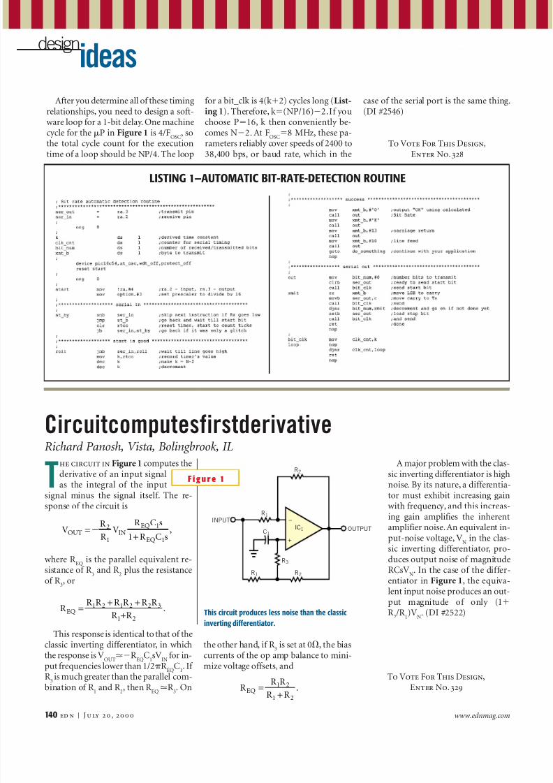
The circuit in Figure 1 computes thederivative of an input signalas the integral of the input
signal minus the signal itself. The re-sponse of the circuit is
where R EQ is the parallel equivalent re-sistance of R 1 and R 2 plus the resistanceof R 3, or
This response is identical to that of theclassic inverting differentiator, in whichthe response is V OUT R EQC1sVIN for in-put frequencies lower than 1/2 R EQC1. If R 3 is much greater than the parallel com-bination of R 1 and R 2, then R EQ R 3. On
the other hand, if R 3 is set at 0 , the biascurrents of the op amp balance to mini-mize voltage offsets, and
A major problem with the clas-sic inverting differentiator is highnoise. By its nature, a differentia-tor must exhibit increasing gainwith frequency, and this increas-ing gain amplifies the inherentamplifier noise.An equivalent in-put-noise voltage, V N in the clas-
sic inverting differentiator, pro-duces output noise of magnitudeRCsVN. In the case of the differ-entiator in Figure 1 , the equiva-lent input noise produces an out-put magnitude of only (1R 2/R 1)VN. (DI #2522)
_
+
IC1 OUTPUT
R2
R2
R3
R1
R1
C1
INPUT
F ig u re 1
CircuitcomputesfirstderivativeRichard Panosh, Vista, Bolingbrook, IL
This circuit produces less noise than the classicinverting differentiator.
To Vote For This Design,Enter No. 328
To Vote For This Design,
Enter No. 329
,sCR 1
sCR V
R R
V1EQ
1EQIN
1
2OUT
+=
.R R
R R R R R R R
21
322121EQ
+
++=
.R R R R R 21
21EQ+
=
LISTING 1—AUTOMATIC BIT-RATE-DETECTION ROUTINE

8/10/2019 2.8-GHz prescaler keeps cost down.pdf
http://slidepdf.com/reader/full/28-ghz-prescaler-keeps-cost-downpdf 3/14
8/10/2019 2.8-GHz prescaler keeps cost down.pdf
http://slidepdf.com/reader/full/28-ghz-prescaler-keeps-cost-downpdf 4/14142 ed n | J u ly 2 0 , 2 0 0 0 www.ednmag.com
ideasdesign
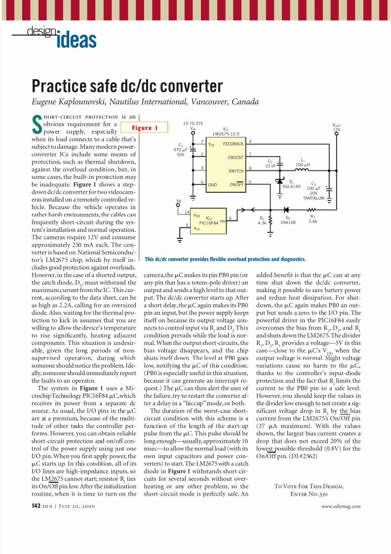
Short-circuit protection is anobvious requirement for apower supply, especially
when its load connects to a cable that’ssubject to damage. Many modern power-converter ICs include some means of protection, such as thermal shutdown,against the overload condition, but, insome cases, the built-in protection may be inadequate. Figure 1 shows a step-
down dc/dc converter for two videocam-eras installed on a remotely controlled ve-hicle. Because the vehicle operates inrather harsh environments, the cables canfrequently short-circuit during the sys-tem’s installation and normal operation.The cameras require 12V and consumeapproximately 250 mA each. The con-verter is based on National Semiconduc-tor’s LM2675 chip, which by itself in-cludes good protection against overloads.However, in the case of a shorted output,the catch diode, D 1, must withstand the
maximum current from the IC. This cur-rent, according to the data sheet, can beas high as 2.2A, calling for an oversizeddiode. Also, waiting for the thermal pro-tection to kick in assumes that you arewilling to allow the device’s temperatureto rise significantly, heating adjacentcomponents. This situation is undesir-able, given the long periods of non-supervised operation, during whichsomeone should notice the problem. Ide-ally, someone should immediately reportthe faults to an operator.
The system in Figure 1 uses a Mi-crochip Technology PIC16F84 C,whichreceives its power from a separate dcsource. As usual, the I/O pins in the Care at a premium, because of the multi-tude of other tasks the controller per-forms. However, you can obtain reliableshort-circuit protection and on/off con-trol of the power supply using just oneI/O pin.When you first apply power, the
C starts up. In this condition, all of itsI/O lines are high-impedance inputs, sothe LM2675 cannot start; resistor R 1 tiesits On/Off pin low.After the initializationroutine, when it is time to turn on the
camera,the C makes its pin PB0 pin (orany pin that has a totem-pole driver) an
output and sends a high level to that out-put. The dc/dc converter starts up. Aftera short delay,the C again makes its PB0pin an input,but the power supply keepsitself on because its output voltage con-nects to control input via R 2 and D 2.Thiscondition prevails while the load is nor-mal.When the output short-circuits, thebias voltage disappears, and the chipshuts itself down. The level at PB0 goeslow, notifying the C of this condition.(PB0 is especially useful in this situation,because it can generate an interrupt re-
quest.) The C can then alert the user of the failure, try to restart the converter af-ter a delay in a “hiccup”mode, or both.
The duration of the worst-case short-circuit condition with this scheme is afunction of the length of the start-uppulse from the C. This pulse should belong enough—usually, approximately 10msec—to allow the normal load (with itsown input capacitors and power con-verters) to start. The LM2675 with a catchdiode in Figure 1 withstands short cir-cuits for several seconds without over-heating or any other problem, so theshort-circuit mode is perfectly safe. An
added benefit is that the C can at any time shut down the dc/dc converter,
making it possible to save battery powerand reduce heat dissipation. For shut-down, the C again makes PB0 an out-put but sends a zero to the I/O pin. Thepowerful driver in the PIC16F84 easily overcomes the bias from R 2, D2, and R 1and shuts down the LM2675. The dividerR 2, D2, R 1 provides a voltage—5V in thiscase—close to the C’s VDD when theoutput voltage is normal. Slight voltagevariations cause no harm to the C,thanks to the controller’s input-diodeprotection and the fact that R 2 limits the
current to the PB0 pin to a safe level.However, you should keep the values inthe divider low enough to not create a sig-nificant voltage drop in R 1 by the biascurrent from the LM2675’s On/Off pin(37 A maximum). With the valuesshown, the largest bias current creates adrop that does not exceed 20% of thelowest possible threshold (0.8V) for theOn/Off pin. (DI #2562)
VDD
VSS
PB0
5V
5
146IC2
PIC16F84
IC1LM2675-12.0
FEEDBACK
CBOOST
SWITCH
ON/OFF
7
2
3
6
15 TO 37VVIN
+C1
470 F50V
VIN
GND
VOUT12V
+C3
100 F
20VTANTALUM
L1100 H
R14.3k
R25.6k
C210 nF
D21N4148
D1SGL4140
5
4
8
1
Figure 1
Practice safe dc/dc converterEugene Kaplounovski, Nautilus International, Vancouver, Canada
This dc/dc converter provides flexible overload protection and diagnostics.
To Vote For This Design,Enter No. 330

8/10/2019 2.8-GHz prescaler keeps cost down.pdf
http://slidepdf.com/reader/full/28-ghz-prescaler-keeps-cost-downpdf 5/14
8/10/2019 2.8-GHz prescaler keeps cost down.pdf
http://slidepdf.com/reader/full/28-ghz-prescaler-keeps-cost-downpdf 6/14

8/10/2019 2.8-GHz prescaler keeps cost down.pdf
http://slidepdf.com/reader/full/28-ghz-prescaler-keeps-cost-downpdf 7/14
8/10/2019 2.8-GHz prescaler keeps cost down.pdf
http://slidepdf.com/reader/full/28-ghz-prescaler-keeps-cost-downpdf 8/14146 ed n | J u ly 2 0 , 2 0 0 0 www.ednmag.com
ideasdesign
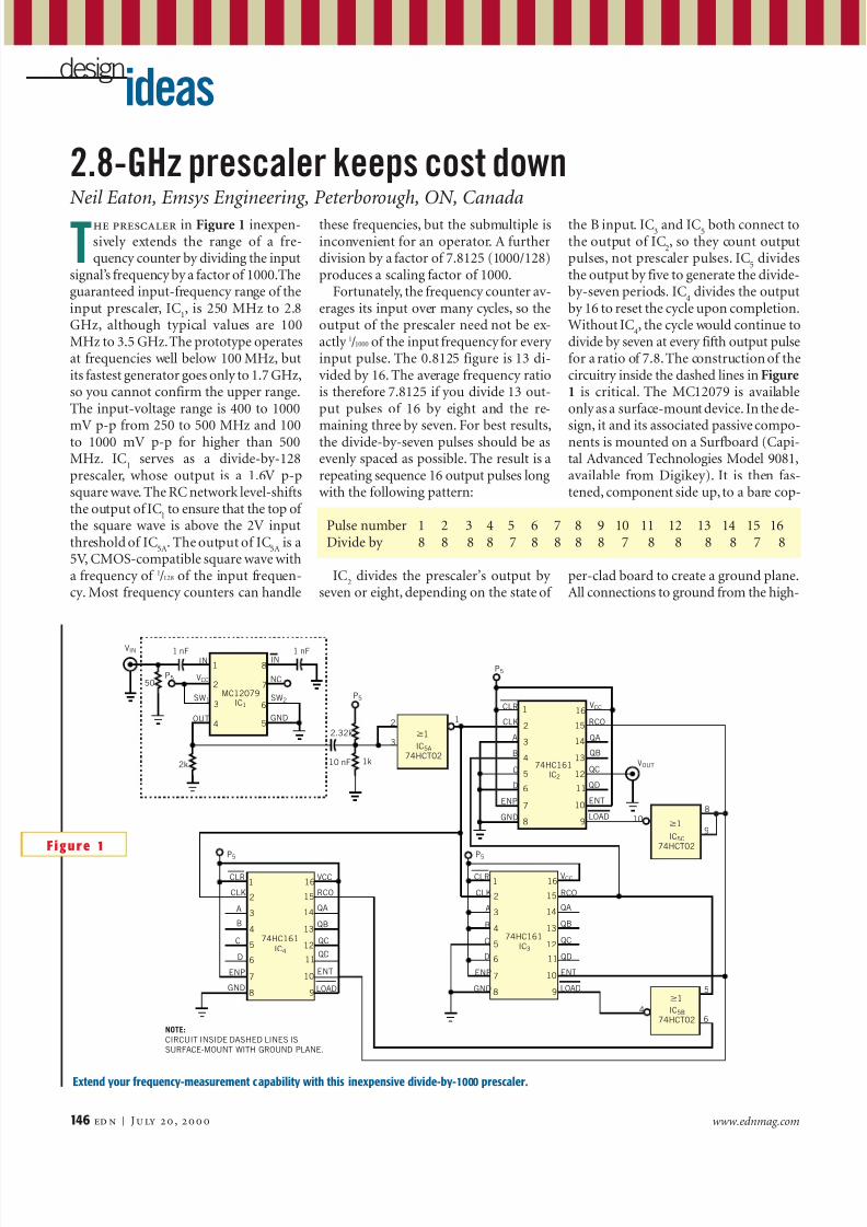
The prescaler in Figure 1 inexpen-sively extends the range of a fre-quency counter by dividing the input
signal’s frequency by a factor of 1000.Theguaranteed input-frequency range of theinput prescaler, IC 1, is 250 MHz to 2.8GHz, although typical values are 100MHz to 3.5 GHz.The prototype operatesat frequencies well below 100 MHz, butits fastest generator goes only to 1.7 GHz,so you cannot confirm the upper range.The input-voltage range is 400 to 1000
mV p-p from 250 to 500 MHz and 100to 1000 mV p-p for higher than 500MHz. IC 1 serves as a divide-by-128prescaler, whose output is a 1.6V p-psquare wave. The RC network level-shiftsthe output of IC 1 to ensure that the top of the square wave is above the 2V inputthreshold of IC 5A. The output of IC 5A is a5V, CMOS-compatible square wave witha frequency of 1/128 of the input frequen-cy. Most frequency counters can handle
these frequencies, but the submultiple isinconvenient for an operator. A furtherdivision by a factor of 7.8125 (1000/128)produces a scaling factor of 1000.
Fortunately, the frequency counter av-erages its input over many cycles, so theoutput of the prescaler need not be ex-actly 1/1000 of the input frequency for every input pulse. The 0.8125 figure is 13 di-vided by 16. The average frequency ratiois therefore 7.8125 if you divide 13 out-put pulses of 16 by eight and the re-
maining three by seven. For best results,the divide-by-seven pulses should be asevenly spaced as possible. The result is arepeating sequence 16 output pulses longwith the following pattern:
IC2 divides the prescaler’s output by seven or eight, depending on the state of
the B input. IC 3 and IC 5 both connect tothe output of IC 2, so they count outputpulses, not prescaler pulses. IC 5 dividesthe output by five to generate the divide-by-seven periods. IC 4 divides the outputby 16 to reset the cycle upon completion.Without IC 4, the cycle would continue todivide by seven at every fifth output pulsefor a ratio of 7.8.The construction of thecircuitry inside the dashed lines in Figure1 is critical. The MC12079 is availableonly as a surface-mount device. In the de-
sign, it and its associated passive compo-nents is mounted on a Surfboard (Capi-tal Advanced Technologies Model 9081,available from Digikey). It is then fas-tened, component side up, to a bare cop-
per-clad board to create a ground plane.All connections to ground from the high-
1
2
3
3
4
4
5
6
7
8 9
10
11
12
13
14
15
16
1
2
3
4
5
6
7
8 9
10
11
12
13
14
15
5
16
6
1
2
3
4
5
6
7
8 9
10
11
12
13
14
15
16
1
2
5
6
7
8
CLR
CLK
A
B
C
D
ENP
GND
CLR
CLK
A
B
C
D
ENP
GND
CLR
CLK
A
B
C
D
ENP
GND
VCC
RCO
QA
QB
QC
QD
ENT
LOAD
VCC
RCO
QA
QB
QC
QD
ENT
LOAD
VCC
RCO
QA
QB
QC
QD
ENT
LOAD
74HC16174HC161
74HC161IC2
IC3IC4
MC12079IC1
NOTE:
CIRCUIT INSIDE DASHED LINES ISSURFACE-MOUNT WITH GROUND PLANE.
IC5A74HCT02
IC5B74HCT02
IC5C74HCT02
4
VOUT
VIN 1 nF 1 nF
1k
P5
P5P5
50
2k
2.32k
10 nF
2
31
1
1
IN
VCC
SW1
OUT
IN
NC
SW2
GND
P5
1
P5
108
9
Figure 1
2.8-GHz prescaler keeps cost down Neil Eaton, Emsys Engineering, Peterborough, ON, Canada
Extend your frequency-measurement capability with this inexpensive divide-by-1000 prescaler.
Pulse number 1 2 3 4 5 6 7 8 9 10 11 12 13 14 15 16Divide by 8 8 8 8 7 8 8 8 8 7 8 8 8 8 7 8

8/10/2019 2.8-GHz prescaler keeps cost down.pdf
http://slidepdf.com/reader/full/28-ghz-prescaler-keeps-cost-downpdf 9/14
8/10/2019 2.8-GHz prescaler keeps cost down.pdf
http://slidepdf.com/reader/full/28-ghz-prescaler-keeps-cost-downpdf 10/14148 ed n | J u ly 2 0 , 2 0 0 0 www.ednmag.com
ideasdesign
speed circuitry go directly to the groundplane using short lengths of copper braid.(Desoldering wick is ideal.) The inputuses a BNC chassis-mount connector
with its shell soldered directly to the
ground plane, and the center pin con-nected to the Surfboard with the shortestpossible wire. The rest of the circuit isnoncritical. To avoid clutter, Figure 1
shows no bypass capacitors, but you
should place them near every IC. (DI#2564)
To Vote For This Design,Enter No. 332
Have you ever wished you coulddistinguish one device’s operatingstate from another’s by the sounds
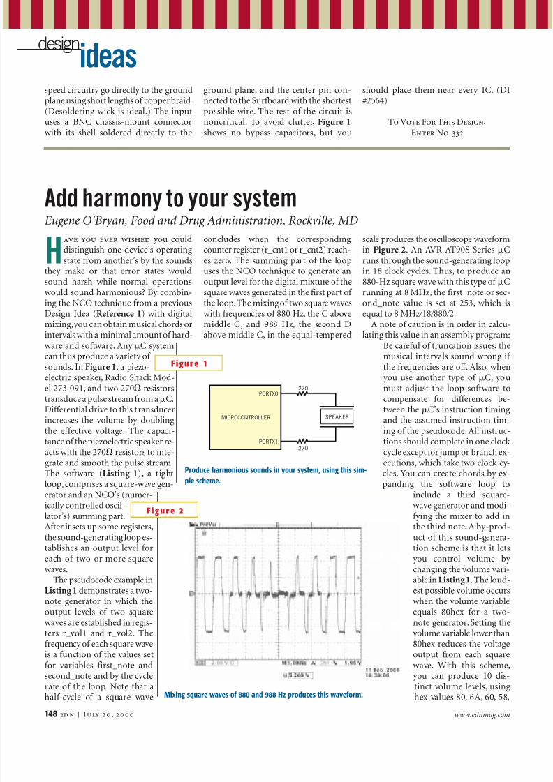
they make or that error states wouldsound harsh while normal operationswould sound harmonious? By combin-ing the NCO technique from a previousDesign Idea ( Reference 1 ) with digitalmixing,you can obtain musical chords orintervals with a minimal amount of hard-ware and software. Any C systemcan thus produce a variety of sounds. In Figure 1 , a piezo-electric speaker, Radio Shack Mod-el 273-091, and two 270 resistorstransduce a pulse stream from a C.
Differential drive to this transducerincreases the volume by doublingthe effective voltage. The capaci-tance of the piezoelectric speaker re-acts with the 270 resistors to inte-grate and smooth the pulse stream.The software ( Listing 1 ), a tightloop, comprises a square-wave gen-erator and an NCO’s (numer-ically controlled oscil-lator’s) summing part.After it sets up some registers,the sound-generating loop es-
tablishes an output level foreach of two or more squarewaves.
The pseudocode example inListing 1 demonstrates a two-note generator in which theoutput levels of two squarewaves are established in regis-ters r_vol1 and r_vol2. Thefrequency of each square waveis a function of the values setfor variables first_note andsecond_note and by the cyclerate of the loop. Note that ahalf-cycle of a square wave
concludes when the correspondingcounter register (r_cnt1 or r_cnt2) reach-es zero. The summing part of the loop
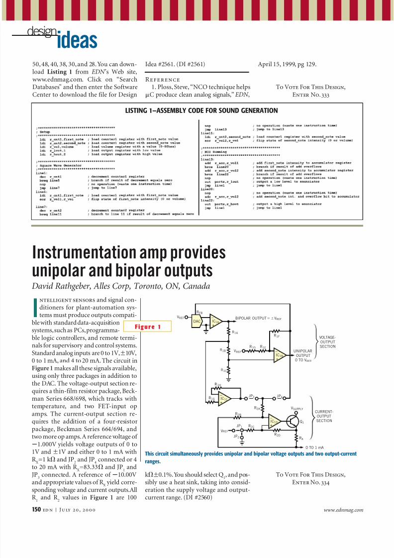
uses the NCO technique to generate anoutput level for the digital mixture of thesquare waves generated in the first part of the loop.The mixing of two square waveswith frequencies of 880 Hz, the C abovemiddle C, and 988 Hz, the second Dabove middle C, in the equal-tempered
scale produces the oscilloscope waveformin Figure 2 . An AVR AT90S Series Cruns through the sound-generating loop
in 18 clock cycles. Thus, to produce an880-Hz square wave with this type of Crunning at 8 MHz, the first_note or sec-ond_note value is set at 253, which isequal to 8 MHz 18 880 2.
A note of caution is in order in calcu-lating this value in an assembly program:
Be careful of truncation issues; themusical intervals sound wrong if the frequencies are off. Also, when you use another type of C, youmust adjust the loop software tocompensate for differences be-
tween the C’s instruction timingand the assumed instruction tim-ing of the pseudocode. All instruc-tions should complete in one clock cycle except for jump or branch ex-ecutions, which take two clock cy-cles. You can create chords by ex-panding the software loop to
include a third square-wave generator and modi-fying the mixer to add inthe third note. A by-prod-uct of this sound-genera-
tion scheme is that it lets you control volume by changing the volume vari-able in Listing 1 . The loud-est possible volume occurswhen the volume variableequals 80hex for a two-note generator. Setting thevolume variable lower than80hex reduces the voltageoutput from each squarewave. With this scheme, you can produce 10 dis-tinct volume levels, usinghex values 80, 6A, 60, 58,
MICROCONTROLLER
PORTX0
PORTX1
SPEAKER
270
270
Figure 1
Add harmony to your systemEugene O’Bryan, Food and Drug Administration, Rockville, MD
Produce harmonious sounds in your system, using this sim-ple scheme.
F ig u re 2
Mixing square waves of 880 and 988 Hz produces this waveform.

8/10/2019 2.8-GHz prescaler keeps cost down.pdf
http://slidepdf.com/reader/full/28-ghz-prescaler-keeps-cost-downpdf 11/14
8/10/2019 2.8-GHz prescaler keeps cost down.pdf
http://slidepdf.com/reader/full/28-ghz-prescaler-keeps-cost-downpdf 12/14
50,48, 40, 38, 30,and 28.You can down-load Listing 1 from EDN ’s Web site,www.ednmag.com. Click on “SearchDatabases” and then enter the Software
Center to download the file for Design
Idea #2561. (DI #2561)
Reference1. Ploss, Steve, “NCO technique helps
C produce clean analog signals,” EDN ,
April 15, 1999, pg 129.
150 ed n | J u ly 2 0 , 2 0 0 0 www.ednmag.com
ideasdesign
LISTING 1—ASSEMBLY CODE FOR SOUND GENERATION
Intelligent sensors and signal con-ditioners for plant-automation sys-tems must produce outputs compati-
ble with standard data-acquisitionsystems,such as PCs,programma-ble logic controllers, and remote termi-nals for supervisory and control systems.Standard analog inputs are 0 to 1V, 10V,0 to 1 mA, and 4 to 20 mA.The circuit inFigure 1 makes all these signals available,using only three packages in addition tothe DAC. The voltage-output section re-
quires a thin-film resistor package, Beck-man Series 668/698, which tracks withtemperature, and two FET-input opamps. The current-output section re-quires the addition of a four-resistorpackage, Beckman Series 664/694, andtwo more op amps.A reference voltage of
1.000V yields voltage outputs of 0 to1V and 1V and either 0 to 1 mA withR X =1 k and JP2 and JP4 connected or 4to 20 mA with R X =83.33 and JP 1 andJP3 connected. A reference of 10.00Vand appropriate values of R X yield corre-sponding voltage and current outputs.AllR 1 and R 2 values in Figure 1 are 100
k 0.1%.You should select Q 1, and pos-sibly use a heat sink, taking into consid-eration the supply voltage and output-current range. (DI #2560)
Instrumentation amp providesunipolar and bipolar outputsDavid Rathgeber, Alles Corp, Toronto, ON, Canada
_
+
VREF
RFB
IC1A
_
+IC1C
_
+IC1D
_
+IC1B
BIPOLAR OUTPUT VREF
R1A
R1B
R1C
R2B
VREF
R2C
R2D
DAC
UNIPOLAROUTPUT
0 TO V REF
VSUPPLY
R1H
R1G
R2A
Q1JP 1
JP 2
JP 3 JP 4
RX
0 TO 1 mA
VREF
R1D R1E
R1F VOLTAGE-OUTPUTSECTION
CURRENT-OUTPUTSECTION
Figure 1
This circuit simultaneously provides unipolar and bipolar voltage outputs and two output-currentranges.
To Vote For This Design,Enter No. 334
To Vote For This Design,Enter No. 333

8/10/2019 2.8-GHz prescaler keeps cost down.pdf
http://slidepdf.com/reader/full/28-ghz-prescaler-keeps-cost-downpdf 13/14

8/10/2019 2.8-GHz prescaler keeps cost down.pdf
http://slidepdf.com/reader/full/28-ghz-prescaler-keeps-cost-downpdf 14/14