26th international symposium on space terahertz … · department of physics (astrophysics),...
TRANSCRIPT
26TH INTERNATIONAL SYMPOSIUM ON SPACE TERAHERTZ TECHNOLOGY, CAMBRIDGE, MA, 16-18 MARCH, 2015.
Investigation of the Dynamic Range ofSuperconducting Nano-Bridge Switches
Boon-Kok Tan∗‡, Ghassan Yassin∗, Ernst Otto† and Leonid Kuzmin†∗Department of Physics (Astrophysics), University of Oxford, Keble Road, Oxford OX1 3RH, UK
†Dept. of Microtechnology & Nanoscience, Chalmers Univ. of Technology, S-41296 Gothenburg, Sweden‡Contact: [email protected], phone +44 1865 273 303
Abstract—We present the design of planar superconductingon/off switch comprising a number of high normal resistancenano-bridges deposited across a the slot of a unilateral finline.We have simulated the performance of this device and haveshown that it has a much larger dynamic range than a singlenano-bridge fabricated from the same material (Niobium Nitride,NbN). The response of a single bridge device was measuredeither directly using a terahertz power meter or by usingsuperconductor-insulator-superconductor (SIS) device as directdetector. In either method, we have demonstrated good agreementbetween simulations and measurements, and therefore confirmedthe integrity of our analysis of the device performance. Wehave recently designed and fabricated multiple nano-bridgessuperconducting switches using 50 µm thick NbN film. Themeasurement of these devices is currently in progress and weexpect to report the results in the forthcoming ISSTT conferencein March.
I. INTRODUCTION
A planar superconducting on/off switch that can be usedto modulate millimetre and sub-millimetre signal with highswitching speed is important for various astronomical in-struments operating in this wavelength regime. It offers apotentially much more efficient and elegant solution againstthe traditionally used rotating quasi-optical or waveguidehalf-wave plates and Faraday rotators [1]. This is particu-larly important for constructing ultra-sensitive polarimeter formeasuring the polarisation state of the Cosmic MicrowaveBackground (CMB) signals. Another important application isthe Bolometric Interferometry instruments where the beamsare combined at RF frequencies. An important advantage of aplanar nano-switch design is that it allows the modulator to beeasily integrated into the detector circuit, offering a compactand low power consumption solution, and therefore enablingthe construction of a large format focal plane array.
II. PLANAR SUPERCONDUCTING ON/OFF SWITCH
In previous papers [2], [3], [4], [5], we have demonstratedthat a nano-switch integrated across the gap of a unilateralfinline can provide an on/off switching operation as the nano-bridge is switched between the normal and superconductingstate using a step current source.
Our superconducting on/off switch is designed to operatein the frequency range of 180–260 GHz. It comprises NbNnano-bridges of 0.5 µm width deposited across a 5 µmwide unilateral finline slot, supported by a 100 µm quartz
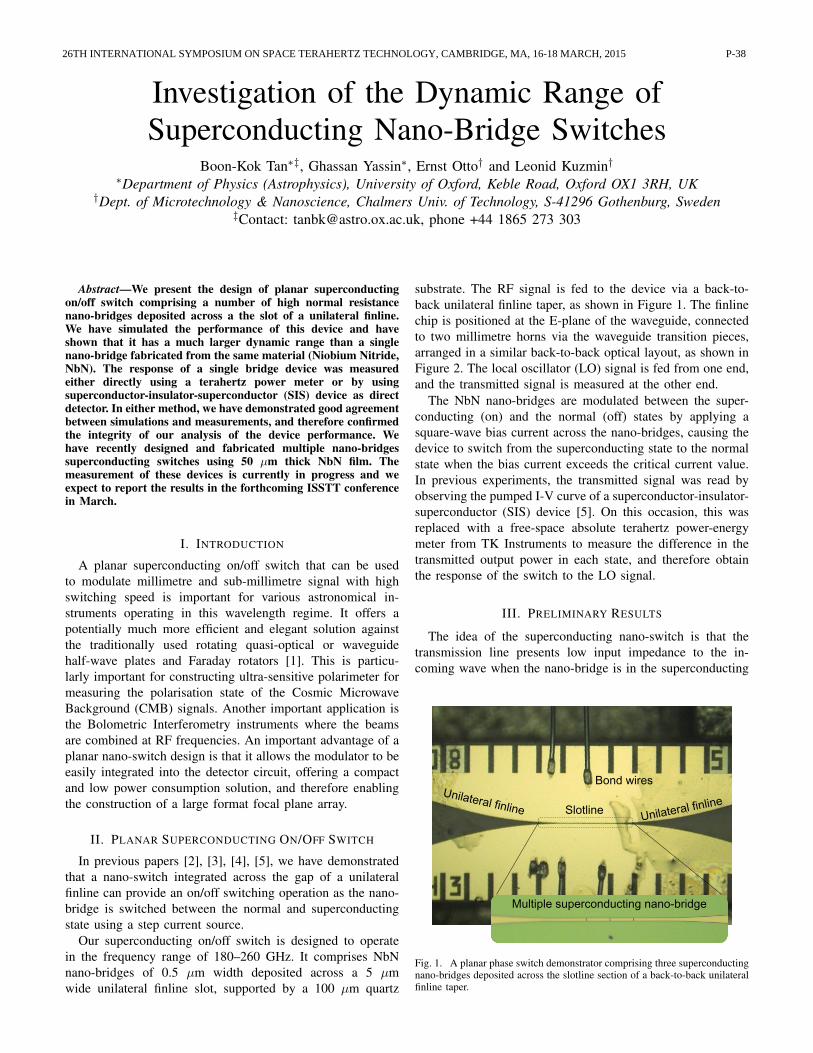
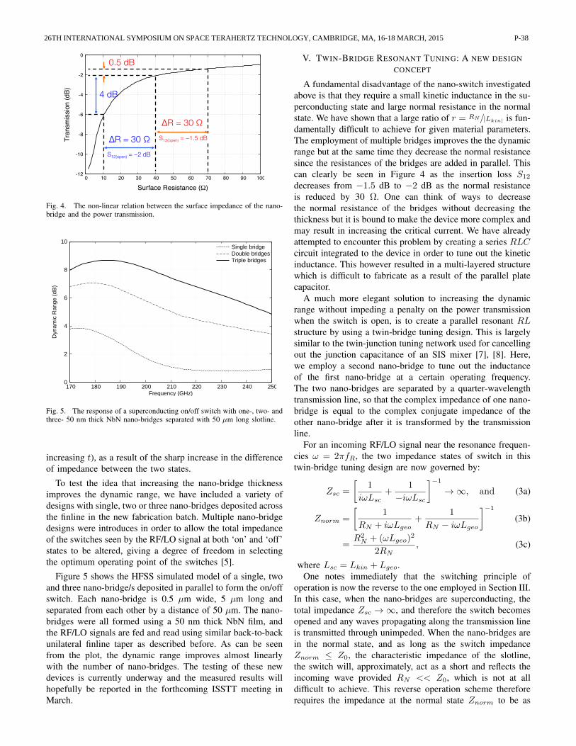
substrate. The RF signal is fed to the device via a back-to-back unilateral finline taper, as shown in Figure 1. The finlinechip is positioned at the E-plane of the waveguide, connectedto two millimetre horns via the waveguide transition pieces,arranged in a similar back-to-back optical layout, as shown inFigure 2. The local oscillator (LO) signal is fed from one end,and the transmitted signal is measured at the other end.
The NbN nano-bridges are modulated between the super-conducting (on) and the normal (off) states by applying asquare-wave bias current across the nano-bridges, causing thedevice to switch from the superconducting state to the normalstate when the bias current exceeds the critical current value.In previous experiments, the transmitted signal was read byobserving the pumped I-V curve of a superconductor-insulator-superconductor (SIS) device [5]. On this occasion, this wasreplaced with a free-space absolute terahertz power-energymeter from TK Instruments to measure the difference in thetransmitted output power in each state, and therefore obtainthe response of the switch to the LO signal.
III. PRELIMINARY RESULTS
The idea of the superconducting nano-switch is that thetransmission line presents low input impedance to the in-coming wave when the nano-bridge is in the superconducting
Unilateral finline
Bond wires
Unilateral finline Slotline
Multiple superconducting nano-bridge
Fig. 1. A planar phase switch demonstrator comprising three superconductingnano-bridges deposited across the slotline section of a back-to-back unilateralfinline taper.
P-3826TH INTERNATIONAL SYMPOSIUM ON SPACE TERAHERTZ TECHNOLOGY, CAMBRIDGE, MA, 16-18 MARCH, 2015

THz Power Meter
Local Oscillator
Phase Switch Block
Feed horn Parabolic Mirrors
Circular to rectangularwaveguide transition
Rectangular to circularwaveguide transition Feed horn Horn
Reflector
Re
Lock-in Amplifier
Computer Readout
4 K cryogenic stage
Fig. 2. Experimental setup for measuring the response of the superconducting on/off switch using a THz power meter.
-1
-0.5
0
0.5
1
200 210 220 230 240 250 260
Dyn
amic
Ran
ge (
dB)
Frequency (GHz)
SimulatedMeasured with power meterMeasured with SIS
Fig. 3. Measured responses of a superconducting switch with 20 nm thickNbN nano-bridge using both the setup with THz power meter (diamond) andthe SIS device (triangle) as power detector. The HFSS simulated response ofthe same device show a similar dynamic range and switching behaviour asthe measured results.
state (switch on) and a high input impedance when the nano-bridge in the normal state. The dynamic range of the switchis therefore primarily determined by the ratio of the normalresistance to the kinetic reactance. A high performance nano-switch therefore will have a high normal resistance (normalstate) and a small kinetic inductance (superconducting state).
We have previously fabricated several superconductingon/off switches with only one nano-bridge of 20 nm thickacross the slotline. Figure 3 shows the measured response ofthe device measured using the new setup shown in Figure 2,along with the previously measured results using the SISdevice as direct detector. As can be seen, the measureddynamic ranges are rather consistent within ±0.5 dB, andmore importantly agree with the responses predicted by theHigh Frequency Structure Simulator (HFSS) model.
However, the dynamic range of these devices was poor sincethe ratio of the normal resistance to the kinetic impedancewas not high enough. This is because when the nano-bridgewas in superconducting state, it did not reflect the incomingsignal efficiently. This can easily be seen by recalling that theimpedance of a superconducting strip is determined by theresistive part of its surface impedance Rsurf ; the geometricinductance Lgeo, and the kinetic inductance Lkin. The laterinductance has a significant value only in the superconductingstate, whereas Rsurf = RN , its thin film normal resistance in
the normal state, and Rsurf ≈ 0 in the superconducting state.The value of these parameters are given by [6]:
RN = ρl/wt, (1a)
Lgeo = 0.2l
[1
2+ ln
(2l
w + t
)+ 0.11
(w + t
l
)]µH, (1b)
Lkin = µ0lλLw
cotht
λL, (1c)
where ρ is the resistivity of the superconductor, λL is theLondon penetration depth, and w, l and t is the width, lengthand thickness of the superconducting strip respectively. For anRF/LO signal at an angular frequency of ω = 2πf , the twoimpedance states are thus given by:
Zsc = iω(Lkin + Lgeo), and (2a)Znorm = RN + iωLgeo. (2b)
For an ideal switch: in the superconducting (‘switch-on’) state,the nano-bridge should has an impedance of Zsc → 0. In thisstate, the load acts as a short, and any waves propagating alongthe transmission line are reflected. In the normal (‘switch-off’)state, the surface impedance is much higher (≈ RN ) and thenano-bridge has an impedance of Znorm → ∞. The switchbecomes opened and the RF/LO signal will pass through thetransmission line with minimum loss.
Initially, we attempted to increase the dynamic range byreducing the nano-bridge thickness down to 20 nm, henceincreasing the normal resistance. But from Equation 1, we canclearly see that the kinetic inductance Lkin depends exponen-tially on t/λL due to the coth (t/λL) term. Decreasing thevalue of t/λL therefore gives rise to a much larger increasein the value of the kinetic inductance than in the normalresistance (which depends linearly on thickness), causing adecrease in the dynamic range. The thickness of the nano-bridges in our new devices was therefore increased from 20 nmto 50 nm so that it is now approaching the London penetrationdepth of the NbN film, hence reducing the kinetic inductanceof the nano-bridges.
IV. HIGH DYNAMIC RANGE BROAD BANDWIDTH DESIGN
An illustration of the ideas described above is shown inFigure 4 which gives the power transmission allowed by theswitch as a function of the surface impedance of the nano-bridges. From the plot, it is clearly seen that the dynamic rangeimproves with the lower surface impedance values (e.g., by
P-38 26TH INTERNATIONAL SYMPOSIUM ON SPACE TERAHERTZ TECHNOLOGY, CAMBRIDGE, MA, 16-18 MARCH, 2015
26TH INTERNATIONAL SYMPOSIUM ON SPACE TERAHERTZ TECHNOLOGY, CAMBRIDGE, MA, 16-18 MARCH, 2015.
-12
-10
-8
-6
-4
-2
0
0 10 20 30 40 50 60 70 80 90 100
Tran
smiss
ion
(dB)
Surface Resistance (1)
ΔR = 30 Ω
4 dB
ΔR = 30 Ω
0.5 dB
S12(open) = −2 dB
S12(open) = −1.5 dB
Fig. 4. The non-linear relation between the surface impedance of the nano-bridge and the power transmission.
0
2
4
6
8
10
170 180 190 200 210 220 230 240 250
Dyn
amic
Ran
ge (
dB)
Frequency (GHz)
Single bridgeDouble bridgesTriple bridges
Fig. 5. The response of a superconducting on/off switch with one-, two- andthree- 50 nm thick NbN nano-bridges separated with 50 µm long slotline.
increasing t), as a result of the sharp increase in the differenceof impedance between the two states.
To test the idea that increasing the nano-bridge thicknessimproves the dynamic range, we have included a variety ofdesigns with single, two or three nano-bridges deposited acrossthe finline in the new fabrication batch. Multiple nano-bridgedesigns were introduces in order to allow the total impedanceof the switches seen by the RF/LO signal at both ‘on’ and ‘off’states to be altered, giving a degree of freedom in selectingthe optimum operating point of the switches [5].
Figure 5 shows the HFSS simulated model of a single, twoand three nano-bridge/s deposited in parallel to form the on/offswitch. Each nano-bridge is 0.5 µm wide, 5 µm long andseparated from each other by a distance of 50 µm. The nano-bridges were all formed using a 50 nm thick NbN film, andthe RF/LO signals are fed and read using similar back-to-backunilateral finline taper as described before. As can be seenfrom the plot, the dynamic range improves almost linearlywith the number of nano-bridges. The testing of these newdevices is currently underway and the measured results willhopefully be reported in the forthcoming ISSTT meeting inMarch.
V. TWIN-BRIDGE RESONANT TUNING: A NEW DESIGNCONCEPT
A fundamental disadvantage of the nano-switch investigatedabove is that they require a small kinetic inductance in the su-perconducting state and large normal resistance in the normalstate. We have shown that a large ratio of r = RN/|Lkin| is fun-damentally difficult to achieve for given material parameters.The employment of multiple bridges improves the the dynamicrange but at the same time they decrease the normal resistancesince the resistances of the bridges are added in parallel. Thiscan clearly be seen in Figure 4 as the insertion loss S12
decreases from −1.5 dB to −2 dB as the normal resistanceis reduced by 30 Ω. One can think of ways to decreasethe normal resistance of the bridges without decreasing thethickness but it is bound to make the device more complex andmay result in increasing the critical current. We have alreadyattempted to encounter this problem by creating a series RLCcircuit integrated to the device in order to tune out the kineticinductance. This however resulted in a multi-layered structurewhich is difficult to fabricate as a result of the parallel platecapacitor.
A much more elegant solution to increasing the dynamicrange without impeding a penalty on the power transmissionwhen the switch is open, is to create a parallel resonant RLstructure by using a twin-bridge tuning design. This is largelysimilar to the twin-junction tuning network used for cancellingout the junction capacitance of an SIS mixer [7], [8]. Here,we employ a second nano-bridge to tune out the inductanceof the first nano-bridge at a certain operating frequency.The two nano-bridges are separated by a quarter-wavelengthtransmission line, so that the complex impedance of one nano-bridge is equal to the complex conjugate impedance of theother nano-bridge after it is transformed by the transmissionline.
For an incoming RF/LO signal near the resonance frequen-cies ω = 2πfR, the two impedance states of switch in thistwin-bridge tuning design are now governed by:
Zsc =
[1
iωLsc+
1
−iωLsc
]−1→∞, and (3a)
Znorm =
[1
RN + iωLgeo+
1
RN − iωLgeo
]−1(3b)
=R2
N + (ωLgeo)2
2RN, (3c)
where Lsc = Lkin + Lgeo.One notes immediately that the switching principle of
operation is now the reverse to the one employed in Section III.In this case, when the nano-bridges are superconducting, thetotal impedance Zsc →∞, and therefore the switch becomesopened and any waves propagating along the transmission lineis transmitted through unimpeded. When the nano-bridges arein the normal state, and as long as the switch impedanceZnorm ≤ Z0, the characteristic impedance of the slotline,the switch will, approximately, act as a short and reflects theincoming wave provided RN << Z0, which is not at alldifficult to achieve. This reverse operation scheme thereforerequires the impedance at the normal state Znorm to be as
P-3826TH INTERNATIONAL SYMPOSIUM ON SPACE TERAHERTZ TECHNOLOGY, CAMBRIDGE, MA, 16-18 MARCH, 2015

-15
-12
-9
-6
-3
0
3
6
9
12
15
170 180 190 200 210 220 230 240 250 260
Dyn
amic
Ran
ge (
dB)
Tra
nsm
issi
on (
dB)
Frequency (GHz)
Dynamic RangeSuperconducting S12
Normal S12
Fig. 6. The response of a superconducting on/off switch with two 50 nmthick NbN nano-bridges separated by a quarter wavelength long slotline.
low as possible. This can be done in several ways, such asincreasing the width of the nano-bridges or using a low normalresistance superconducting material such as Niobium (Nb). Infact, use of a wider nano-bridge also eliminates the need forusing electron-beam lithography to fabricate these devices.
Figure 6 shows the HFSS predicted dynamic range andthe power transmission in both superconducting and normalstate for a switch comprising two 50 nm thick NbN nano-bridge separated by a quarter-wavelength slotline, depositedacross the slotline section of the back-to-back finline taper.The nano-bridge is 5 µm long and 2 µm wide now, in orderto reduce the normal resistance RN , and therefore increasethe dynamic range. As can clearly be seen from the plot, atthe resonance frequency of 215 GHz, the dynamic range ishigher than 10 dB, while the power transmission when theswitch is superconducting is approaching 0 dB. This improvessignificantly the power transmission of the switch and providesan ideal switch design for applications where the incomingsignal is weak. It is however evident from the plot that theoperating bandwidth of the resonant switch is narrower thanthat of the multiple bridge switch described in Section IV.
VI. CONCLUSION
We have presented a design of a planar superconductingon/off switch comprising nano-bridges deposited across the
electrodes of a slotline. Preliminary experimental results havebeen presented and agree well with electromagnetic modelsimulations. The low dynamic range of the single nano-bridgeswitch was caused mainly due to its small thickness since itcaused the residual kinetic inductance to be too high in thesuperconducting state. In this paper, we therefore proposedtwo solutions to improve the dynamic range of the switch, byemploying multiple nano-bridges across the same slotline. Bycarefully choosing the separation distance between the nano-bridges, we can either design a broadband solution with slightloss of transmission or a resonant narrow band design withoutcompromising the power transmission of the switch. In eithercase, we predict a dynamic range of more than 10 dB. Weare currently in the process of measuring the response of thebroadband design with a thicker NbN film, and the measuredresults shall be reported in the forthcoming ISSTT conferencein March.
REFERENCES
[1] P. A. R. Ade, D. T. Chuss, S. Hanany, V. Haynes, B. G. Keating, A. Kogut,J. E. Ruhl, G. Pisano, G. Savini, and E. J. Wollack, “Polarizationmodulators for CMBPol,” Journal of Physics Conference Series, vol. 155,p. 012006, Mar. 2009.
[2] P. K. Grimes, G. Yassin, L. S. Kuzmin, P. D. Mauskopf, E. Otto,M. E. Jones, and C. E. North, “Investigation of planar switches forlarge format CMB polarization instruments,” in Society of Photo-OpticalInstrumentation Engineers (SPIE) Conference Series, vol. 6275 of Societyof Photo-Optical Instrumentation Engineers (SPIE) Conference Series,July 2006.
[3] G. Yassin, L. S. Kuzmin, P. K. Grimes, M. Tarasov, E. Otto, and P. D.Mauskopf, “An integrated superconducting phase switch for cosmologyinstruments,” Physica C Superconductivity, vol. 466, pp. 115–123, Nov.2007.
[4] L. Kuzmin, M. Tarasov, E. Otto, A. Kalabukhov, G. Yassin, P. Grimes,and P. Mauskopf, “Superconducting subterahertz fast nanoswitch,” SovietJournal of Experimental and Theoretical Physics Letters, vol. 86, pp. 275–277, Oct. 2007.
[5] B.-K. Tan, G. Yassin, L. Kuzmin, E. Otto, H. Merabet, and C. North,“A Superconducting Millimetre Switch with Multiple Nano-Bridges,” inTwenty Fifth International Symposium on Space Terahertz Technology,Apr. 2014.
[6] G. Yassin, P. Kittara, A. Jiralucksanawong, S. Wangsuya, J. Leech, andM. Jones, “A High Performance Horn for Large Format Focal PlaneArrays,” in Proceedings of the Eighteenth International Symposium onSpace Terahertz Technology, pp. 199–+, 2007.
[7] V. I. Belitskii, M. A. Tarasov, S. A. Kovtoniuk, L. V. Filippenko, andO. V. Kaplunenko, “Low noise completely quasioptical SIS receiverfor radioastronomy at 115 GHz,” International Journal of Infrared andMillimeter Waves, vol. 13, pp. 389–396, Apr. 1992.
[8] P. Grimes, Design and analysis of 700 GHz Finline Mixers. PhD thesis,University of Cambridge, United Kingdom, 2006.
P-38 26TH INTERNATIONAL SYMPOSIUM ON SPACE TERAHERTZ TECHNOLOGY, CAMBRIDGE, MA, 16-18 MARCH, 2015