2.674 (s16) lecture 10: mems applications and … · please see the second image on page . ......
TRANSCRIPT

Graphene
2.674
Jeehwan Kim
1
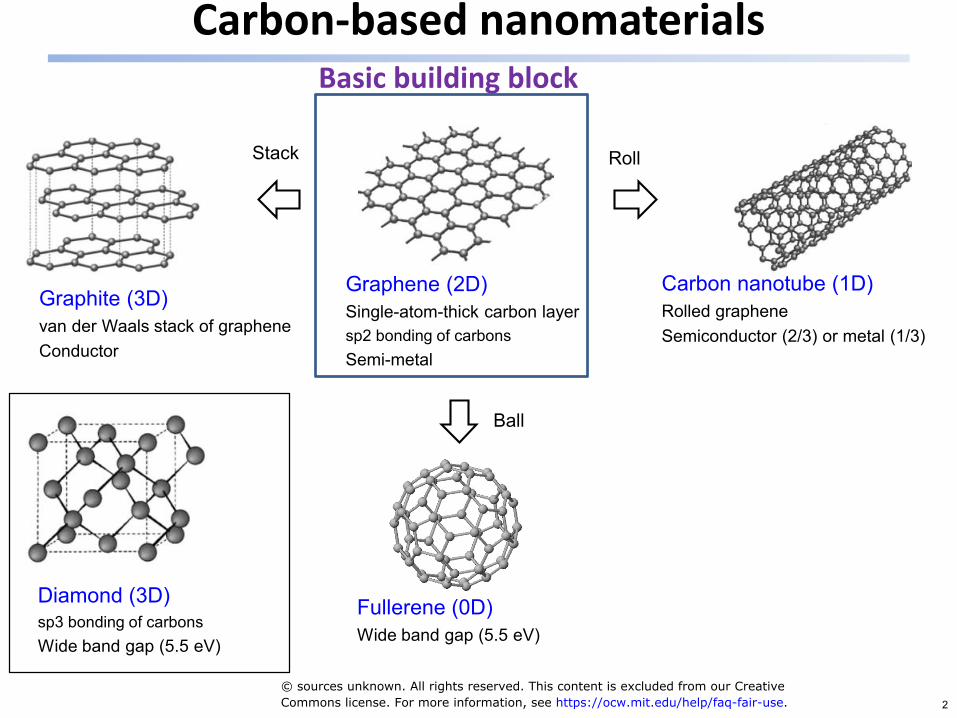
Carbon-based nanomaterials
Graphene (2D)Single-atom-thick carbon layersp2 bonding of carbonsSemi-metal
Diamond (3D)sp3 bonding of carbonsWide band gap (5.5 eV)
Graphite (3D)van der Waals stack of grapheneConductor
Carbon nanotube (1D)Rolled grapheneSemiconductor (2/3) or metal (1/3)
Fullerene (0D)Wide band gap (5.5 eV)
Ball
Stack Roll
Basic building block
© sources unknown. All rights reserved. This content is excluded from our CreativeCommons license. For more information, see https://ocw.mit.edu/help/faq-fair-use. 2

What is graphene?
© sources unknown. All rights reserved. This content is excludedfrom our Creative Commons license. For more information,see https://ocw.mit.edu/help/faq-fair-use.
3
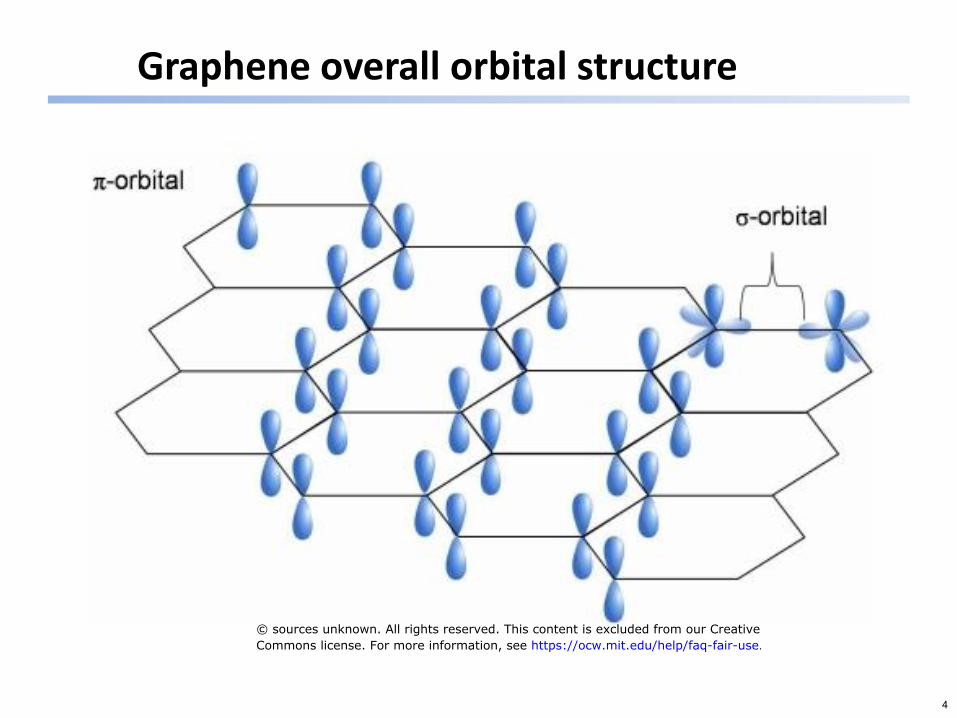
Graphene overall orbital structure
© sources unknown. All rights reserved. This content is excluded from our CreativeCommons license. For more information, see https://ocw.mit.edu/help/faq-fair-use.
4

CNT vs Graphene
CNT Graphene
Electrical conductivity
~100,000 cm2/VS >100,000 cm2/VS
Thermalconductivity
~5000W/K.m ~5000W/K.m
Young’s modulus 0.9 ~1.1TPa 1 TPa
Transparency O O
Flexibility O O
Electron mobility(cm2/Vs)
Electricalcharacteristics
Copper 5,770 Conductor
Silver 9,490 Conductor
GaAs 6,000 Semiconductor
Si 1,350 Semiconductor
Graphene/CNT >100,000 Semi-metal5
Challenges for Carbon Nanotube Applications
• Control the diameter of nanotubes and chirality.
• Purification/sorting methods required for uniform CNT
• Large scale integration
• Placement/alignment methods required for long-range order
• ASSEMBLY, ASSEMBLY, ASSEMBLY!!!• Graphene Lab 11
1 µm (10 trenches)1 µm (10 trenches)
Pitch = 100 nm
Wtr = 70 nm
1 µm (5 trenches)1 µm (5 trenches)
Pitch = 200 nm
Wtr = 100 nm
H. Park et al., Nature Nanotechnology 7, 787(2012)© Macmillan Publishers Limited. All rights reserved. This content is excluded from our CreativeCommons license. For more information, see https://ocw.mit.edu/help/faq-fair-use.
6

Discovery of carbon allotropes
• 1985: Curl, Kroto, Smalley discovered fullerene (Nobel, Physics 1996)
• 1991: Iijima discovered single wall carbon nanotubes.
• 2010 A. Geim and K. Novoselov (Nobel physics on Graphene) Scotch tape method
Why so difficult?© sources unknown. All rights reserved. This content is excluded from our CreativeCommons license. For more information, see https://ocw.mit.edu/help/faq-fair-use.
7
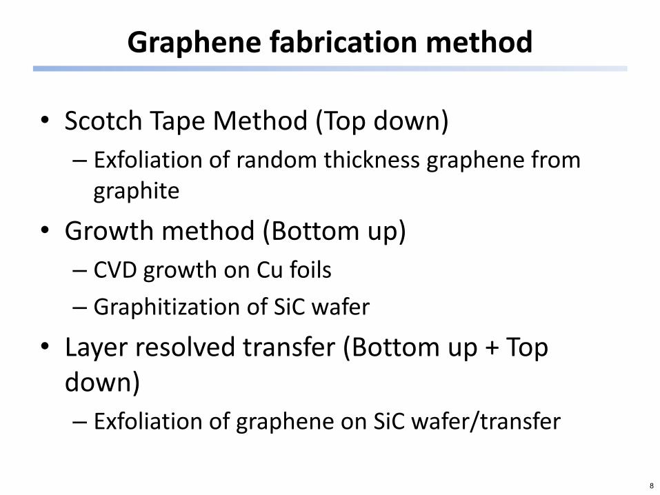
Graphene fabrication method
• Scotch Tape Method (Top down)
– Exfoliation of random thickness graphene from graphite
• Growth method (Bottom up)
– CVD growth on Cu foils
– Graphitization of SiC wafer
• Layer resolved transfer (Bottom up + Top down)
– Exfoliation of graphene on SiC wafer/transfer
8
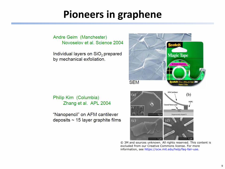
Pioneers in graphene
© 3M and sources unknown. All rights reserved. This content isexcluded from our Creative Commons license. For moreinformation, see https://ocw.mit.edu/help/faq-fair-use.
9
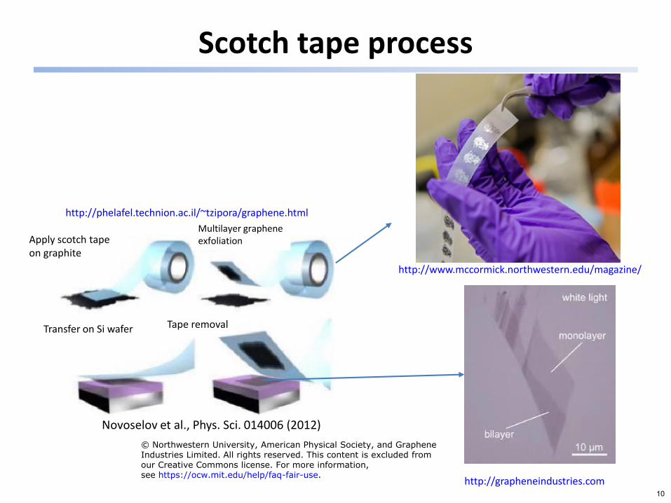
Scotch tape process
Novoselov et al., Phys. Sci. 014006 (2012)
Apply scotch tape on graphite
Multilayer grapheneexfoliation
Transfer on Si wafer Tape removal
http://www.mccormick.northwestern.edu/magazine/
http://phelafel.technion.ac.il/~tzipora/graphene.html
http://grapheneindustries.com
© Northwestern University, American Physical Society, and Graphene Industries Limited. All rights reserved. This content is excluded from our Creative Commons license. For more information,see https://ocw.mit.edu/help/faq-fair-use.
10
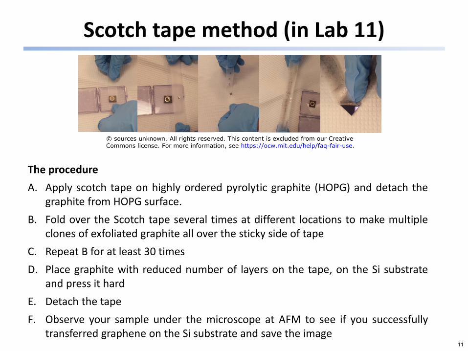
Scotch tape method (in Lab 11)
The procedure
A. Apply scotch tape on highly ordered pyrolytic graphite (HOPG) and detach thegraphite from HOPG surface.
B. Fold over the Scotch tape several times at different locations to make multipleclones of exfoliated graphite all over the sticky side of tape
C. Repeat B for at least 30 times
D. Place graphite with reduced number of layers on the tape, on the Si substrateand press it hard
E. Detach the tape
F. Observe your sample under the microscope at AFM to see if you successfullytransferred graphene on the Si substrate and save the image
© sources unknown. All rights reserved. This content is excluded from our CreativeCommons license. For more information, see https://ocw.mit.edu/help/faq-fair-use.
11

Graphene flakes on oxide
Nanoscale, 2012,4, 5527-5537
Nanotechnology 22 (2011) 365306
Optical image
Monolayer Bilayer
Thickness of monolayer graphenetypically measured by AFM: 0.5-1nm
Theoretical thickness of graphene: 0.35 nm
© IOP Publishing. All rights reserved. This content is excluded fromour Creative Commons license. For more information,see https://ocw.mit.edu/help/faq-fair-use.
12
CVD growth
This image has been removed due to copyright restrictions.Please see the second image on page https://www.comsol.com/blogs/synthesizing-graphene-chemical-vapor-deposition/.
13
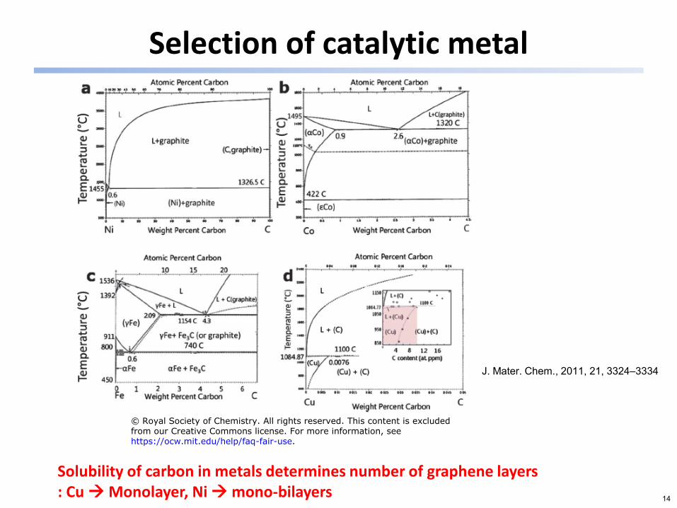
Selection of catalytic metal
J. Mater. Chem., 2011, 21, 3324–3334
Solubility of carbon in metals determines number of graphene layers: Cu Monolayer, Ni mono-bilayers
© Royal Society of Chemistry. All rights reserved. This content is excluded from our Creative Commons license. For more information, see https://ocw.mit.edu/help/faq-fair-use.
14

Growth mechanism
J. Mater. Chem., 2011, 21, 3324–3334
© Royal Society of Chemistry. All rights reserved. This content is excluded from our CreativeCommons license. For more information, see https://ocw.mit.edu/help/faq-fair-use.
15
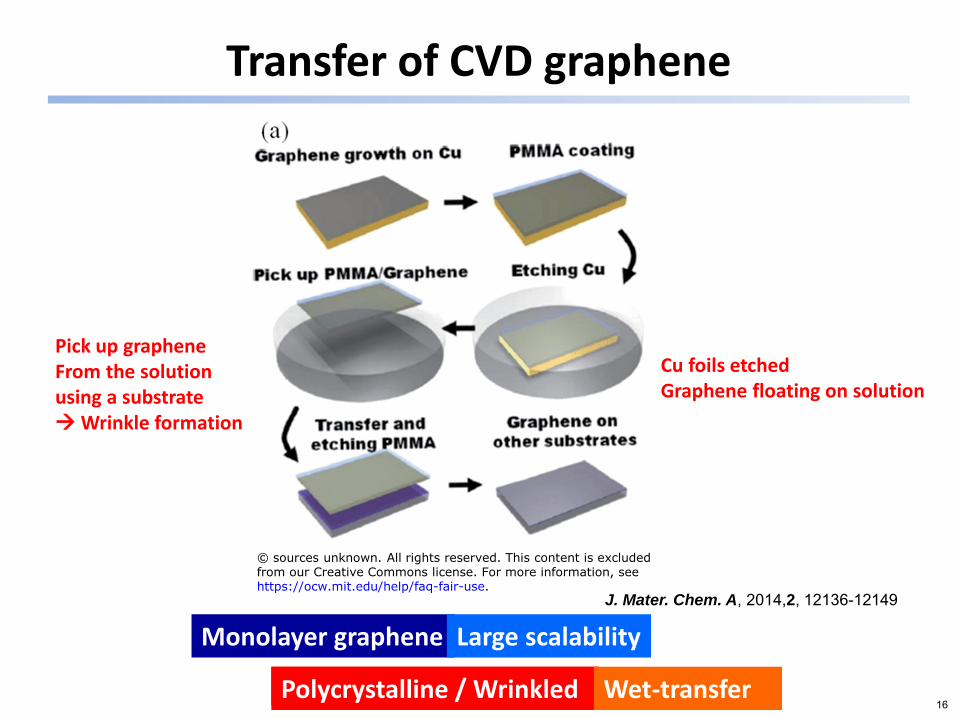
Transfer of CVD graphene
Monolayer graphene
Polycrystalline / Wrinkled
Large scalability
Polycrystalline / Wrinkled Wet-transfer
J. Mater. Chem. A, 2014,2, 12136-12149
Cu foils etchedGraphene floating on solution
Pick up grapheneFrom the solutionusing a substrateWrinkle formation
© sources unknown. All rights reserved. This content is excludedfrom our Creative Commons license. For more information, seehttps://ocw.mit.edu/help/faq-fair-use.
16
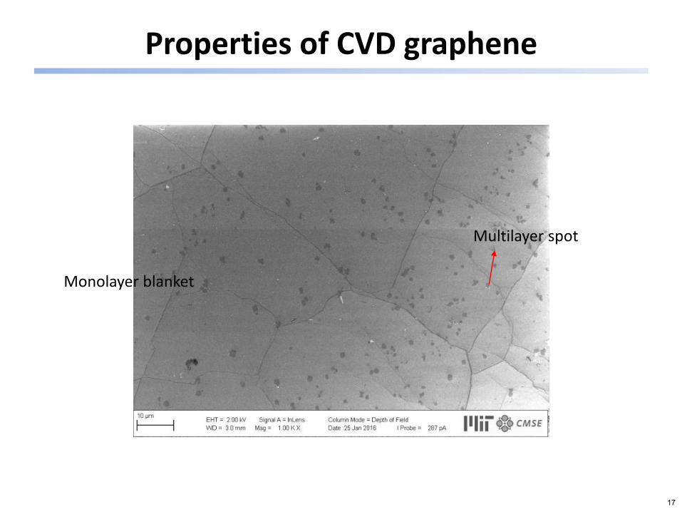
Properties of CVD graphene
Multilayer spot
Monolayer blanket
17

Graphitization of SiC
SiC substrate
Si sublimationat 1500oC
1 ML
2 ML
Graphene
carbon buffer
SiC
Raman Map
2 ML1 ML
• When SiC substrates are annealed at high temperature (above 1300 °C), Si atoms selectively desorb from the surface and the C atoms left behind naturally form monolayer graphene
– Single-oriented flat graphene obtainable
Flat / Single-oriented Un-transferrable / Expensive
© sources unknown. All rights reserved. This content is excluded from our CreativeCommons license. For more information, see https://ocw.mit.edu/help/faq-fair-use.
18

Properties of SiC graphene
LEEM 2 ML
1 ML
Monolayer sheet due to Si sublimation at surface
Additional stripe due to Si sublimation at step edge
© sources unknown. All rights reserved. This content is excluded from our CreativeCommons license. For more information, see https://ocw.mit.edu/help/faq-fair-use.
19

Layer resolved SiC graphene transfer
Jeehwan Kim et al., “Layer-resolved graphene transfer via engineered strain-layers”,
Science, Vol. 342, 833 (2013)
© Science. All rights reserved. This content is excluded from our Creative Commonslicense. For more information, see https://ocw.mit.edu/help/faq-fair-use.
20

Thin film mechanics
Binding energy(meV/atom)
Ni-G ~ 140
G-SiC ~100SiC
Graphene
Ni
Binding E (G-SiC)
Binding E (G-Ni)
SiC
Graphene
Ni (0.5-1 GPa)Applying high stress Into the interface
SiC
Crack open& propagate
© sources unknown. All rights reserved. This content is excluded from our CreativeCommons license. For more information, see https://ocw.mit.edu/help/faq-fair-use.
21
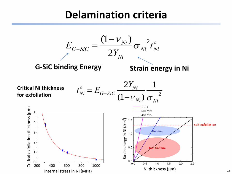
Delamination criteria
cNiNi
Ni
NiSiCG t
YE 2
2
)1(
200 400 600 800 10000
1
2
3
4
5
Cri
tica
l exf
olia
tio
n t
hic
kne
ss (
m)
Internal stress in Ni (MPa)
G-SiC binding Energy Strain energy in Ni
2
1
)1(
2
NiNi
NiSiCG
cNi
YEt
Critical Ni thicknessfor exfoliation
22
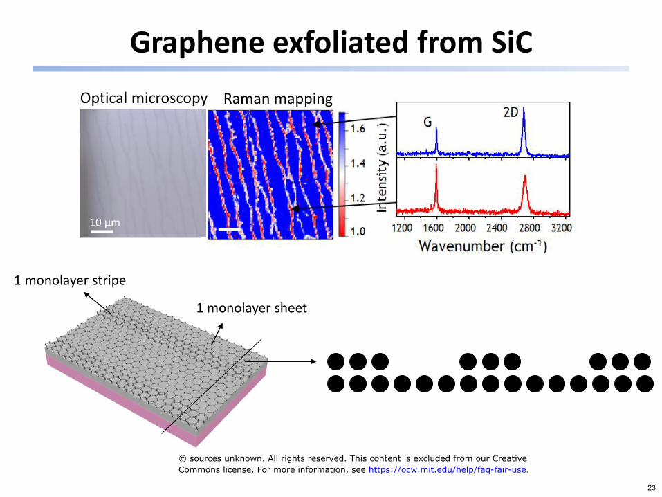
Graphene exfoliated from SiC
10 μm
Optical microscopy Raman mapping
Monolayered area : 80%
1 monolayer sheet
1 monolayer stripe
© sources unknown. All rights reserved. This content is excluded from our CreativeCommons license. For more information, see https://ocw.mit.edu/help/faq-fair-use.
23

Separation of bilayer stripes
Au
Tape
NiGraphene sheet
Gr Gr
BE (Au-G) > BE (G-G)BE (Au-G) << BE (Ni-G)
Binding energy(meV/atom)
G-G ~ 45
Ni-G ~ 140
Au-G ~ 60
Manipulation of binding energy contrast among materials
10 μm
10 μm
This image has been removeddue to copyright restrictions.Please see http://target.scene7com/is/ image/Target/10994898.
© sources unknown. All rights reserved. This content is excluded from our CreativeCommons license. For more information, see https://ocw.mit.edu/help/faq-fair-use. 24
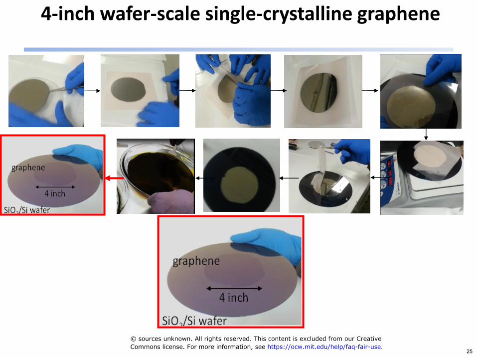
4-inch wafer-scale single-crystalline graphene
© sources unknown. All rights reserved. This content is excluded from our CreativeCommons license. For more information, see https://ocw.mit.edu/help/faq-fair-use.
25

Scotch Tape
graphene
CVD
grapheneSiC graphene
Layer-resolve
Transfer
Monolayer Control UncontrollableSelf-limiting
(>95% ML)
Self-limiting
(1.2 ML)
Crystalline orientationSingle but less than
poly grain sizePolycrystal Single
Flatness Pristine Wrinkle from foils Same as SiC wafer
Large-scalability ~50 μmDepending on CVD
reactor sizeWafer size
Transfer efficiency Uncontrollable Wet-transfer Un-transferrable
Process cleanliness Dry-transfer Wet-transferNo transfer
invovled
Price Cheap CheapExtremely
expensive
Summary of graphene fabrication methods
Excellent Good Poor
J. Kim*, H. Park*, J. Hannon, S. Bedell, K. Fogel, D. Sadana, C. Dimitrak
“Layer-resolved graphene transfer via engineered strain-layers”, Science, Vol. 342, 833 (2013)26

Application of graphene
Nanoscale, 2015, 7, 4598-4810
© Royal Society of Chemistry. All rights reserved. This content is excluded from our CreativeCommons license. For more information, see https://ocw.mit.edu/help/faq-fair-use.
27

Future of graphene electronics
Graphene roadmap : Nature (2013)
Future of graphene electronics
© Nature. All rights reserved. This content is excluded from our Creative Commonslicense. For more information, see https://ocw.mit.edu/help/faq-fair-use.
28

In Lab 11
1) Experience Nobel Prize winning method to fabricate graphene from graphite
2) Image different types of graphene using AFM
- Measure thickness of monolayer graphene
- Find thinnest graphene among graphene flakes you made
3) Obtain atomic image of graphene using STM
29

Quiz (May 3)
• Examples
– Short answer questions• What kind of chemical bond between PDMS and glass slide results
in after O2 plasma treatment and bonding of the two surfaces?
Covalent bonding
– Fill blanks• The ratio of inertial force over viscous force defined as, ρdu/ µ.
This is (Reynolds) number
– True or False• Single atom can be resolved by SEM. F
– Multiple choices
30

MIT OpenCourseWarehttps://ocw.mit.edu
2.674 / 2.675 Micro/Nano Engineering LaboratorySpring 2016
For information about citing these materials or our Terms of Use, visit: https://ocw.mit.edu/terms.