document2
TRANSCRIPT

Obtaining a pure sinusoidal waveform usingmultilevel inverters with increased higher
voltage levels using NPC H-BridgeS.DEVI LAVANYA1, Dr.KIRUBAKARAN.D2
1Research scholar in Prist University, Tanjavur-613 403, Tamilnadu-India1E&C Dept., Associate professor, Nadgir Institute of Engineering and technology,Bangalore-560072 Karnataka-India,
2Professor/EEE, St. Joseph’s Institute of Technology, Chennai -119, Tamil [email protected], [email protected]
ABSTRACT: This paper presents a Multilevel inverter that consists of a standard 3-leg two level inverter cascaded with two new neutral point clamped H-bridge inverter in series with eachinverter leg with a single dc voltage source of 300V. The control signals for this multilevel inverter is obtained by using carrierbased PWM technique. The proposed multilevel inverter is usedto obtain a pure sinusoidal waveform which is verified using MATLAB/SIMULINK software. The results of the simulation,the output waveform of three phase voltage and phase currentobtained are pure sinusoidal therefore the proposed topology canbe implemented for HVDC transmission and induction motor drives using the dc source obtained from solar panels which is converted to ac using proposed topology. The proposed topology is concentrated to increase the voltage levels of the output using asingle dc source. The new NPC flying capacitor H-Bridgeinverter is invented in this paper and its advantages arediscussed in this paper by doing so a pure sine wave is obtained.
KEYWORDS: New NPC flying capacitor H-bridge inverter, multilevel inverter, HVDC, two level flying capacitor inverter,sinusoidal waveform, Solar panels.
I.. INTRODUCTI ON
A multilevel inverter is a power electronic converterbuilt to synthesize a desired AC voltage from several levelsof dc voltages in which the DC levels a r e obtained from b a t t e r i e s , solar cells, capacitors, etc. In this paper, theproposed topology uses a new two NPC H-bridge inverter in series with each leg of two level inverter and suitablePWM technique is used to obtain a pure sinusoidalwaveform which is not in the form of multilevel which isthe actual meaning of multilevel inverter. The prototype istested with resistive inductive load one with NPC and otherwithout NPC. This analysis is carried out without using anylow pass or high pass filter.
Several topologies and Several PWM techniques werecarried out which were complicating the entire control andpower circuit. The proposed topology implements a simplecarrier based PWM technique implemented with a new two NPC H-bridge inverter and increased voltage levels.To obtain a quality output voltage or a current waveformwith a minimum amount of ripple content, they require various pulse width modulation (PWM) strategies, which increase the switching frequency of the power devices.In the case of multi level inverters, as the number of
voltage levels increases the harmonic content of theoutput voltage waveform decreases, even without using any pulse width modulation technique. As the switchingfrequency is reduced the power losses are also minimized, and thereby increasing the efficiency of the system. The paper is focused to obtain a pure sinusoidal waveform using asingle dc voltage source without using any filters. Theproposed topology implements the development of sinusoidal A C voltage can be obtained us in g a single DCvoltage source at desired output voltage and frequency byusing a power electronics device that is called an inverter.Industrial applications of inverters are for adjustable-speed AC drives, UPS (uninterruptible power supply), HVDC transmission lines. DC power inputs that inverters can usethe solar panels as a dc supply and show that the proposedtopology can be used for industries.
II. SIMULATION ANALYSIS
The power circuit diagram of a three phase full bridgeinverter is shown in Fig (1). The dc supply is obtained f r o ma b a t t e r y o r f r o m s o l a r p a n e l s . The p o w e rcircuit is obtained by using 30 switches, SEVEN switches for each of the three phases which forms the circuit. Each step is defined as a change in the time operation for each IGBT to the next IGBT in proper sequence. For one cycle 360 degree, each step would be of 60 degree interval for a six step inverter. Fig (1) shows the power circuit diagram of a three phase bridge inverter using seven IGBTs in each phase. Capacitors are connected as shown in figure serving as DC voltage source. Several topologies and several PWM techniques are going on research for multilevel inverters to obtain a pure sinusoidal waveform. Each step is defined as a change in the time operation for each IGBT to the next IGBT in proper sequence. For one cycle 360 degree, each step would be of 60 degree interval for a six step inverter. Fig (1) shows the power circuit diagram of a three phase bridge inverter using seven IGBTs in each phase. Several topologies and several PWM techniques are going on research for multilevel inverters to obtain a pure sinusoidal waveform. The proposed topology solves this problem. The analysis is carried out using MATLAB/SIMULINK model. The proposed PWM technique is quite similar to a carrier based PWM. The prototype is tested with two types of load such as R and RL load
978-1-4673-2818-0/13/$31.00 ©2013 IEEE

H-BRIDGE 1 H-BRIDGE 2Figure (1) MATLAB/SIMULINK circuit for proposed three-phase multilevel inverter with two NPC H-
bridge inverter.
Figure (2) The PWM signals given to a two level inverter
S11
S12
S13
S14
S21
S22
S23
S24
S31
S32
S33
S34
S101
S102
S103
S104
S201
S202
S203
S204
S301
S302
S303
S304
1a
1f
2a
2f
3a
3f
300v
15f150v
15f150v
1ohm
1ohm
15f70v
15f 70v
15f70v
15f70v
15f70v
15f70v
15f35v
15f35v
15f35v
15f35v
15f35v
15f35v
100 ohm 1e-10 henry
Discrete,s = 5e-005 s
powergui
VabcIabc
A
B
C
a
bc
A B C
A B C
In1
In2
In3
S11
S12
S13
S14
S21
S22
S23
S24
S31
S32
S33
S34
In1
In2
In3
S11
S12
S13
S14
S21
S22
S23
S24
S31
S32
S33
S34
1a
2a
3a
1f
2f
3f
gm
CE
gm
CE
gm
CE
gm
CE
gm
CE
gm
CE
gm
CE
gm
CE
gm
CE
gm
CE
gm
CE
gm
CE
gm
CE
gm
CE
gm
CE
gm
CE
gm
CEg
m
CE
gm
CE
gm
CE
gm
CE
gm
CE
gm
CE
gm
CE
gm
CE
gm
CE
gm
CE
gm
CE
gm
CE
gm
CE
-T-
[l3a]
-T-
-T-
-T-
[l2a]
-T-
-T-[l24]
[l14]
[l33]
[l23]
[l13]
[l32]
[l22]
[l12]
[l31]
-T-
[l21]
[l11]
[l3f]
-T-
[l2f] -T-
[l1f]
-T-
-T-
-T-
[l34]
[l1a]
-T-[l3a]
[l2f]
-T-
-T-
[l2a]
[l1f]
-T--T-
-T--T-
-T--T-
-T--T-
-T--T-
[l3f]
-T--T-
-T--T-
-T--T-
-T--T-
-T--T-
-T-
[l1a]i+ -
63f
52f
41f
33a
22a
11a
In1
In2
In3
S11
S12
S13
S14
S21
S22
S23
S24
S31
S32
S33
S34
>
>
>
NOT
NOT
LogicalOperator4
NOT
NOT
NOT
LogicalOperator10
NOT
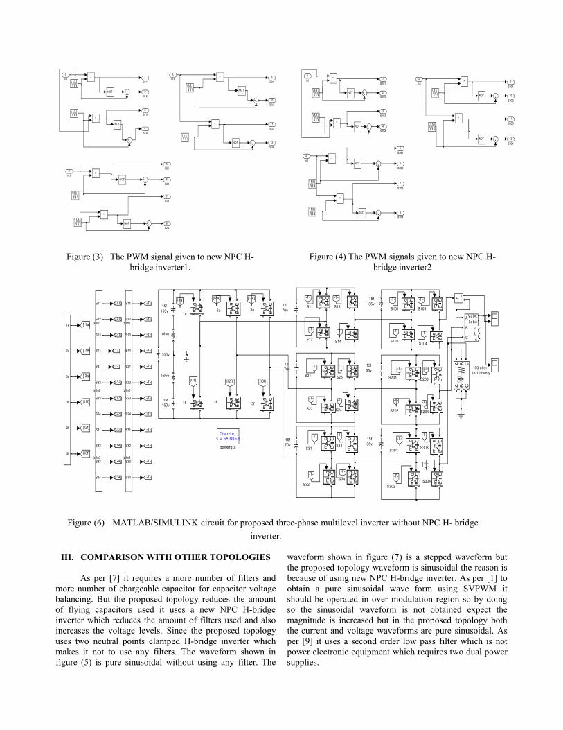
Figure (3) The PWM signal given to new NPC H-bridge inverter1.
Figure (4) The PWM signals given to new NPC H-bridge inverter2
Figure (6) MATLAB/SIMULINK circuit for proposed three-phase multilevel inverter without NPC H- bridgeinverter.
III. COMPARISON WITH OTHER TOPOLOGIES
As per [7] it requires a more number of filters and more number of chargeable capacitor for capacitor voltage balancing. But the proposed topology reduces the amount of flying capacitors used it uses a new NPC H-bridge inverter which reduces the amount of filters used and also increases the voltage levels. Since the proposed topology uses two neutral points clamped H-bridge inverter which makes it not to use any filters. The waveform shown in figure (5) is pure sinusoidal without using any filter. The
waveform shown in figure (7) is a stepped waveform but the proposed topology waveform is sinusoidal the reason is because of using new NPC H-bridge inverter. As per [1] to obtain a pure sinusoidal wave form using SVPWM it should be operated in over modulation region so by doing so the sinusoidal waveform is not obtained expect the magnitude is increased but in the proposed topology both the current and voltage waveforms are pure sinusoidal. As per [9] it uses a second order low pass filter which is not power electronic equipment which requires two dual power supplies.
12S34
11S33
10S32
9S31
8S24
7S23
6S22
5S21
4S14
3S13
2S12
1S11
>
>
>
>>
>
NOT
NOT
NOT
NOT
NOT
NOT
3In3
2In2
1In1
12S304
11S303
10S302
9S301
8S204
7S203
6S202
5S201
4S104
3S103
2S102
1S101
>
>
>
>>
>
NOT
NOT
NOT
NOT
NOT
NOT
3In3
2In2
1In1
S11
S12
S13
S14
S21
S22
S23
S24
S31S33
S34
S101
S102
S103
S104
S201
S202
S203
S204
S301
S302
S303
S304
1a
1f
2a
2f
3a
3f
300v
15f150v
15f150v
1ohm
1ohm
15f70v
15f70v
15f70v
15f35v
15f35v
15f35v
100 ohm 1e-10 henry
S32
Discrete,Ts = 5e-005 s
powergui
VabcIabc
A
B
C
abc
A B C
A B C
In1
In2
In3
S11
S12
S13
S14
S21
S22
S23
S24
S31
S32
S33
S34
In1
In2
In3
S11
S12
S13
S14
S21
S22
S23
S24
S31
S32
S33
S34
1a
2a
3a
1f
2f
3f
gm
CE
gm
CE
gm
CE
gm
CE
gm
CE
gm
CE
gm
CE
gm
CE
gm
CE
gm
CE
gm
CE
gm
CE
gm
CE
gm
CE
gm
CE
gm
CE
gm
CEg
m
CE
gm
CE
gm
CE
gm
CE
gm
CE
gm
CE
gm
CE
gm
CE
gm
CE
gm
CE
gm
CE
gm
CE
gm
CE
-T-
[l3a]
-T-
-T-
-T-
[l2a]
-T-
-T-[l24]
[l14]
[l33]
[l23]
[l13]
[l32]
[l22]
[l12]
[l31]
-T-
[l21]
[l11]
[l3f]
-T-
[l2f] -T-
[l1f]
-T-
-T-
-T-
[l34]
[l1a]
-T-[l3a]
[l2f]
-T-
-T-
[l2a]
[l1f]
-T--T-
-T--T-
-T--T-
-T--T-
-T--T-
[l3f]
-T--T-
-T--T-
-T--T-
-T--T-
-T--T-
-T-
[l1a]i+ -

Figure (5) The three pha
IV. DESIGN OF THE PROTOPOLOGY
The input dc voltage given to the proposto Vdc=300volts which is clamped to +Vdc/capacitors, which is given as input to the twoinput given to the NPC H-bridge inverter is given by means of chargeable capacitor. ThH-bridge is equal to +Vdc/8 and -Vdc/8 voltcapacitance used is 15 farads. The output ovoltage obtained is around 100 volts.
Figure (7) The three phase output vCurrent waveform of proposed top
NPC.
ase voltage and phase current waveform of proposed topo
OPOSED
sed topology is equal /2 and -Vdc/2 using o level inverter. The + Vdc/4 and -Vdc/4
he input given to thets. The value of the of the peak to peak
voltage and phasepology without
V. SCOPE OF THE PRO
In future we can use the proac power generation using solar psuitable for industries as there iswhich is required for ac powertopology can be used for ac powertopology a new NPC H-bridge ifuture it may be carried out to redif a suitable PWM technique is invlevels so the proposed new NPC there and thereby reducing one Nplace. As the proposed topologycompared with when we use singletwo level inverter the amount ofwhere the output voltage of singreduces the number of componentsusing solar panels.
VI. CONC
The proposed topology coninverter cascaded with a two newsupply given to the circuit is a singobtained is sinusoidal. The simulatinductive load. The output of thsinusoidal and this output is giobtained is pure sinusoidal obtainthis topology can be used for acused in industries. The simulSimulink/matlab software. The pphase multilevel inverter which sh
ology.
OPOSED TOPOLOGY
posed topology for three phase panels as dc source and make it s a scarcity of water in future r generation so the proposed r generation. As in the proposed s invented in this paper so in
duce the number of components vented to increase the number of
H-bridge inverter can be used NPC H-bridge inverter at that y increases the output voltage e NPC H-Bridge in series with a f solar panels can be reduced
gle solar cell is 0.6volts which s required to obtain a dc supply
LUSION
nsists of a 3-phase two level w NPC H-bridge inverter. The gle dc power source. The output tion is carried out with resistive he proposed topology is pure iven to the load. The output ed using a single dc source, so power generation and can be
lation is carried out usingproposed topology is a three-hows the comparison with and

without NPC in H-bridge inverter. The new NPC flying capacitor H-Bridge inverter has been invented in this paper and its advantages are as explained.
REFERENCES
[1] A General Space Vector PWM Algorithm for multilevel inverters including operation in overmodulation region. IEEE
Transactions on power electronics. Volume 22 . NO.2. 2007.[2] A.V.RAVI KUMAR, G.RAVI KUMAR International
Journal of Engineering Research and Applications (IJERA)[3] P. J. Link, “Minimizing electric bearing currents in
ASD systems,” IEEE Ind. Applicat. Mag., vol. 5, pp. 55–66, July/Aug. 1999.
[4] D. Rendusara, E. Cengelci, P. Enjeti, V. Stefanovic, andW. Gray, “Analysis of common mode voltage -“Neutral shift ” in medium voltagePWM adjustable speed drive (MV-ASD) systems,” in Proc. IEEE PESC’99, 1999, CDROM.
[5] L. Palma, L. Morán, and R. Wallace and cost effective solution to reduce motor bearing currents in PWM inverter drives,” in Proc. ISIE 2000, pp. 425–429.
[6] H. Zhang, A. von Jouanne, and A. Wallace,“Multilevel inverter modulation schemes to eliminate common-mode voltages,” in Conf. Rec.IEEE-IAS Annu. Meeting, 1998, CD-ROM.
[7] ] International Journal of Engineering and Technology Volume 2 No. 7, July, 2012 ISSN: 2049-3444 © 2012 – IJET Publications UK. All rights reserved. 1131 Investigations on Three Phase Five Level Flying Capacitor Multilevel InverterR.Balamurugan1, S.P.Natarajan2, R.Bensraj3.
[8] M. Venu Madhav “ MATLAB based Analysis and Simulation of Multilevel Inverters” International Journal of Computer Applications (0975 – 8887) Volume 39– No.4, February 2012.
[9] R.S. Kanchan, M.R. Baiju, K.K. Mohapatra, P.P.Ouseph and K. Gopakumar “Space vector PWM signal generation for multilevel inverters using only the sampled amplitudes of reference phase voltages”
[10] International Conference on Emerging Frontiers in Technology for Rural Area (EFITRA) 2012 Proceedings published in International Journal of Computer Applications® (IJCA) “Performance of Sinusoidal Pulse Width Modulation based Three level inverter’’.
AUTHORS BIBILOGRAPHY
S.Devi Lavanya born on 15/8/1980 received the B.E. degree from BMSCE college VTU University in 2005 and received M.E. from Sathyabama University in 2009 and working in NDIET as Associateprofessor in E&C Department, Now currently research scholar in PRIST
University Tanjavur, Tamilnadu-India. Areas of interest in multilevel inverters and dc-dc converters.
Dr.Kirubakaran.D has obtained his PhDfrom Anna University in 2010 And M.E.from Barthidasan University in 2000. His areas of interest are AC-AC Converters for induction heating. He has 13 years ofteaching experience. He is a life member ofISTE.