256 10 sdi ii ip core design example user guide - altera · pdf file2.6 video pattern...
TRANSCRIPT
Intel® Arria® 10 SDI II IP CoreDesign Example User Guide
Updated for Intel® Quartus® Prime Design Suite: 17.0
SubscribeSend Feedback
UG-20076 | 2017.05.08Latest document on the web: PDF | HTML
Contents
1 SDI II Design Example Quick Start Guide........................................................................ 31.1 Directory Structure................................................................................................. 31.2 Hardware and Software Requirements....................................................................... 61.3 Generating the Design.............................................................................................71.4 Simulating the Design............................................................................................. 81.5 Compiling and Testing the Design ............................................................................ 8
1.5.1 Connection and Settings Guidelines...............................................................91.5.2 Design Limitations for Serial Loopback Design...............................................11
2 SDI II Design Example Detailed Description.................................................................. 132.1 Parallel Loopback Design Examples......................................................................... 142.2 Serial Loopback Design Examples............................................................................182.3 Design Components.............................................................................................. 222.4 Clocking Scheme Signals....................................................................................... 252.5 Interface Signals...................................................................................................282.6 Video Pattern Generator Parameters........................................................................392.7 Hardware Setup....................................................................................................402.8 Simulation Testbench............................................................................................ 41
A SDI II IP Core Design Example User Guide Archives......................................................44
B Revision History for SDI II IP Core Design Example User Guide................................... 45
Contents
Intel® Arria® 10 SDI II IP Core Design Example User Guide2
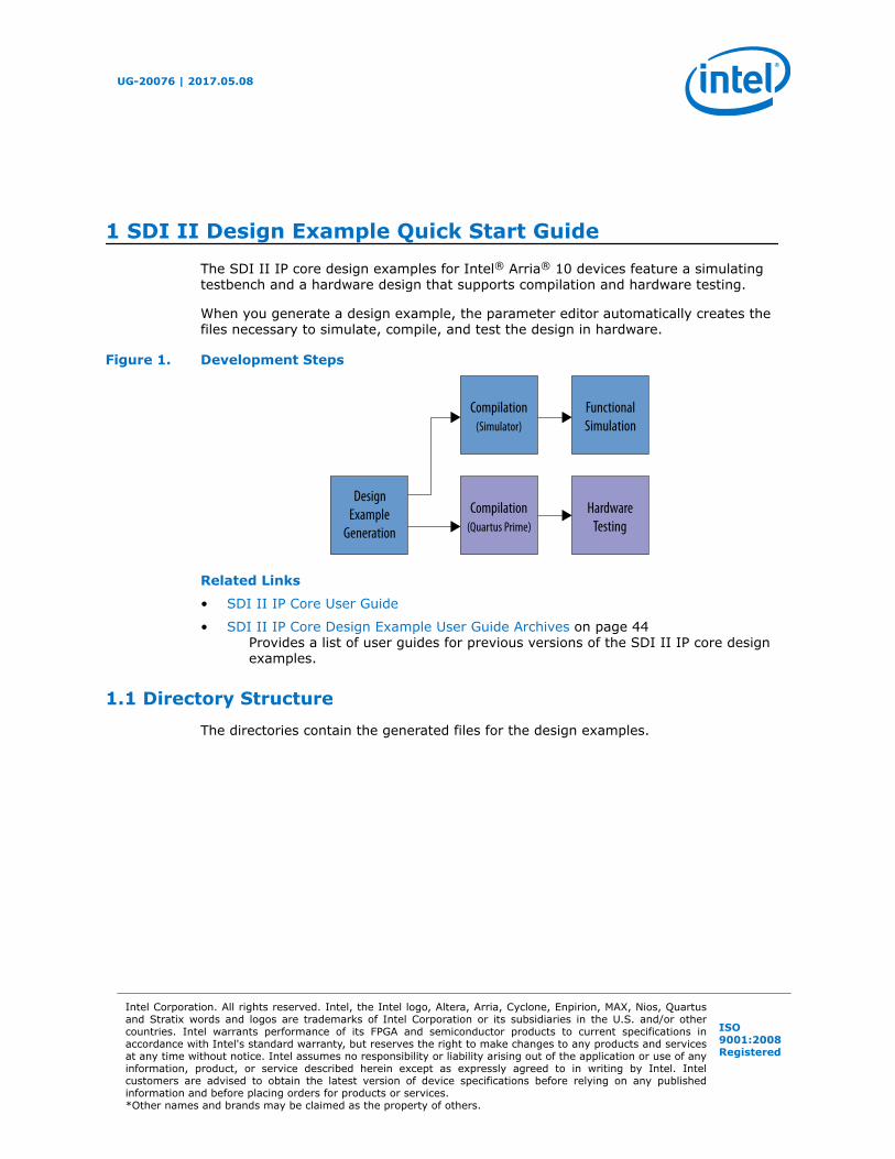
1 SDI II Design Example Quick Start GuideThe SDI II IP core design examples for Intel® Arria® 10 devices feature a simulatingtestbench and a hardware design that supports compilation and hardware testing.
When you generate a design example, the parameter editor automatically creates thefiles necessary to simulate, compile, and test the design in hardware.
Figure 1. Development Steps
DesignExample
Generation
Compilation(Simulator)
FunctionalSimulation
Compilation(Quartus Prime)
HardwareTesting
Related Links
• SDI II IP Core User Guide
• SDI II IP Core Design Example User Guide Archives on page 44Provides a list of user guides for previous versions of the SDI II IP core designexamples.
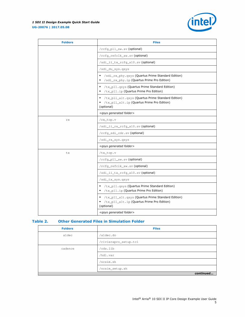
1.1 Directory Structure
The directories contain the generated files for the design examples.
UG-20076 | 2017.05.08
Intel Corporation. All rights reserved. Intel, the Intel logo, Altera, Arria, Cyclone, Enpirion, MAX, Nios, Quartusand Stratix words and logos are trademarks of Intel Corporation or its subsidiaries in the U.S. and/or othercountries. Intel warrants performance of its FPGA and semiconductor products to current specifications inaccordance with Intel's standard warranty, but reserves the right to make changes to any products and servicesat any time without notice. Intel assumes no responsibility or liability arising out of the application or use of anyinformation, product, or service described herein except as expressly agreed to in writing by Intel. Intelcustomers are advised to obtain the latest version of device specifications before relying on any publishedinformation and before placing orders for products or services.*Other names and brands may be claimed as the property of others.
ISO9001:2008Registered

Figure 2. Directory Structure for the Design Examples
<Design Example>
db/qdb
quartus
sdi_ii_a10_demo.qpf
sdi_ii_a10_demo.qsf
rtl
sdi_ii_a10_demo.v
sdi_ii_a10_demo.sdc
edge_detector.sv
clock_heartbeat.sv
a10_reconfig_arbiter.sv (optional)
vid_pattgen (for serial loopback design)
rx (for simplex mode design)
tx (for simplex mode design)
du (for duplex mode design)
loopback (for parallel loopback design)
<clk_ctrl.qsys generated>(optional)
<pll_148 qsys generated> (optional)
clk_ctrl.qsys (optional)
pll_148.qsys (optional)
aldec
cadence
mentor
simulation
synopsys
testbench
tpg.ctrl.tcl (optional)
hwtest(for serial loopback design)
Table 1. Other Generated Files in RTL Folder
Folders Files
vid_pattgen /sdi_ii_colorbar_gen.v
/sdi_ii_ed_vid_pattgen.v
/sdi_ii_makeframe.v
/sdi_ii_patho_gen.v
/jtag.sdc
/pattgen_ctrl.qsys
<qsys generated folder>
loopback /loopback_top.v
/fifo/sdi_ii_ed_loopback.sdc
/fifo/sdi_ii_ed_loopback.v
/pfd/clock_crossing.v (optional)
/pfd/pfd.sdc (optional)
/pfd/pfd.v (optional)
/reclock/sdi_reclock.v (optional)
/reclock/pid_controller.v (optional)
du /du_top.v
/sdi_ii_rx_rcfg_a10.sv (optional)
/rcfg_sdi_cdr.sv (optional)
continued...
1 SDI II Design Example Quick Start Guide
UG-20076 | 2017.05.08
Intel® Arria® 10 SDI II IP Core Design Example User Guide4
Folders Files
/rcfg_pll_sw.sv (optional)
/rcfg_refclk_sw.sv (optional)
/sdi_ii_tx_rcfg_a10.sv (optional)
/sdi_du_sys.qsys
• /sdi_rx_phy.qsys (Quartus Prime Standard Edition)• /sdi_rx_phy.ip (Quartus Prime Pro Edition)
• /tx_pll.qsys (Quartus Prime Standard Edition)• /tx_pll.ip (Quartus Prime Pro Edition)
• /tx_pll_alt.qsys (Quartus Prime Standard Edition)• /tx_pll_alt.ip (Quartus Prime Pro Edition)(optional)
<qsys generated folder>
rx /rx_top.v
/sdi_ii_rx_rcfg_a10.sv (optional)
/rcfg_sdi_cdr.sv (optional)
/sdi_rx_sys.qsys
<qsys generated folder>
tx /tx_top.v
/rcfg_pll_sw.sv (optional)
/rcfg_refclk_sw.sv (optional)
/sdi_ii_tx_rcfg_a10.sv (optional)
/sdi_tx_sys.qsys
• /tx_pll.qsys (Quartus Prime Standard Edition)• /tx_pll.ip (Quartus Prime Pro Edition)
• /tx_pll_alt.qsys (Quartus Prime Standard Edition)• /tx_pll_alt.ip (Quartus Prime Pro Edition)(optional)
<qsys generated folder>
Table 2. Other Generated Files in Simulation Folder
Folders Files
aldec /aldec.do
/rivierapro_setup.tcl
cadence /cds.lib
/hdl.var
/ncsim.sh
/ncsim_setup.sh
continued...
1 SDI II Design Example Quick Start Guide
UG-20076 | 2017.05.08
Intel® Arria® 10 SDI II IP Core Design Example User Guide5

Folders Files
<cds_libs folder>
mentor /mentor.do
/msim_setup.tcl
synopsys /vcs/filelist.f
/vcs/vcs_setup.sh
/vcs/vcs_sim.sh
/vcsmx/synopsys_sim_setup
/vcsmx/vcsmx_setup.sh
/vcsmx/vcsmx_sim.sh
testbench tb_top.v
rx_checker/sdi_ii_tb_rx_checker.v
rx_checker/tb_data_compare.v
rx_checker/tb_dual_link_sync.v
rx_checker/tb_fifo_line_test.v
rx_checker/tb_frame_locked_test.sv
rx_checker/tb_rxsample_test.v
rx_checker/tb_trs_locked_test.sv
rx_checker/tb_txpll_test.sv
rx_checker/tb_vpid_check.v
tb_control/sdi_ii_tb_control.v
tb_control/tb_clk_rst.v
tb_control/tb_data_delay.v
tb_control/tb_serial_delay.sv
tb_control/tb_tasks.v
tb_checker/sdi_ii_tb_tx_checker.v
tb_checker/tb_serial_check_counter.v
tb_checker/tb_serial_descrambler.v
tb_checker/tb_tx_clkout_check.v
vid_pattgen/sdi_ii_colorbar_gen.v
vid_pattgen/sdi_ii_ed_vid_pattgen.v
vid_pattgen/sdi_ii_makeframe.v
vid_pattgen/sdi_ii_patho_gen.v
1.2 Hardware and Software Requirements
Intel uses the following hardware and software to test the design examples:
1 SDI II Design Example Quick Start Guide
UG-20076 | 2017.05.08
Intel® Arria® 10 SDI II IP Core Design Example User Guide6

Hardware
• Intel Arria 10 GX FPGA Development Kit
• SDI Signal Generator
• SDI Signal Analyzer
• SubMiniature version B (SMB) to Bayonet Neill–Concelman (BNC) cables forsingle-rate and triple-rate designs, or BNC to BNC cables for multi-rate designs
• VIDIO™ FMC Development Module VIDIO-12G-A (Nextera 12G SDI FMC daughtercard) for multi-rate designs
Software
• Intel Quartus Prime (for hardware testing)
• ModelSim* - Intel FPGA Edition, ModelSim-SE, NCSim (Verilog only), Riviera-Pro,or VCS (Verilog only)/VCS-MX simulator
1.3 Generating the Design
Use the SDI II parameter editor in the Quartus Prime software to generate the designexamples.
Figure 3. Generating the Design Flow
Start ParameterEditor
Specify IP Variationand Select Device
SelectDesign Parameters
InitiateDesign Generation
Specify Example Design
1. Create a project targeting Arria 10 device family and select the desired device.
2. In the IP Catalog, locate and double-click SDI II IP Core. The New IP Variantor New IP Variation window appears.
3. Specify a top-level name for your custom IP variation. The parameter editor savesthe IP variation settings in a file named <your_ip>.ip or <your_ip>.qsys.
4. Click OK. The parameter editor appears.
5. On the IP tab, select your desired IP settings. The generated design example willbe based on your settings.
6. On the Design Example tab, select Simulation to generate the testbench, andselect Synthesis to generate the hardware design example.
You must select at least one of these options to generate the design example files.
7. For Generate File Format, select Verilog or VHDL.
8. For Target Development Kit, select Arria 10 GX FPGA Development Kit. Youmay change the target device using the Change Target Device parameter if yourboard revision does not match the grade of the default targeted device.
9. Click Generate Example Design.
1 SDI II Design Example Quick Start Guide
UG-20076 | 2017.05.08
Intel® Arria® 10 SDI II IP Core Design Example User Guide7
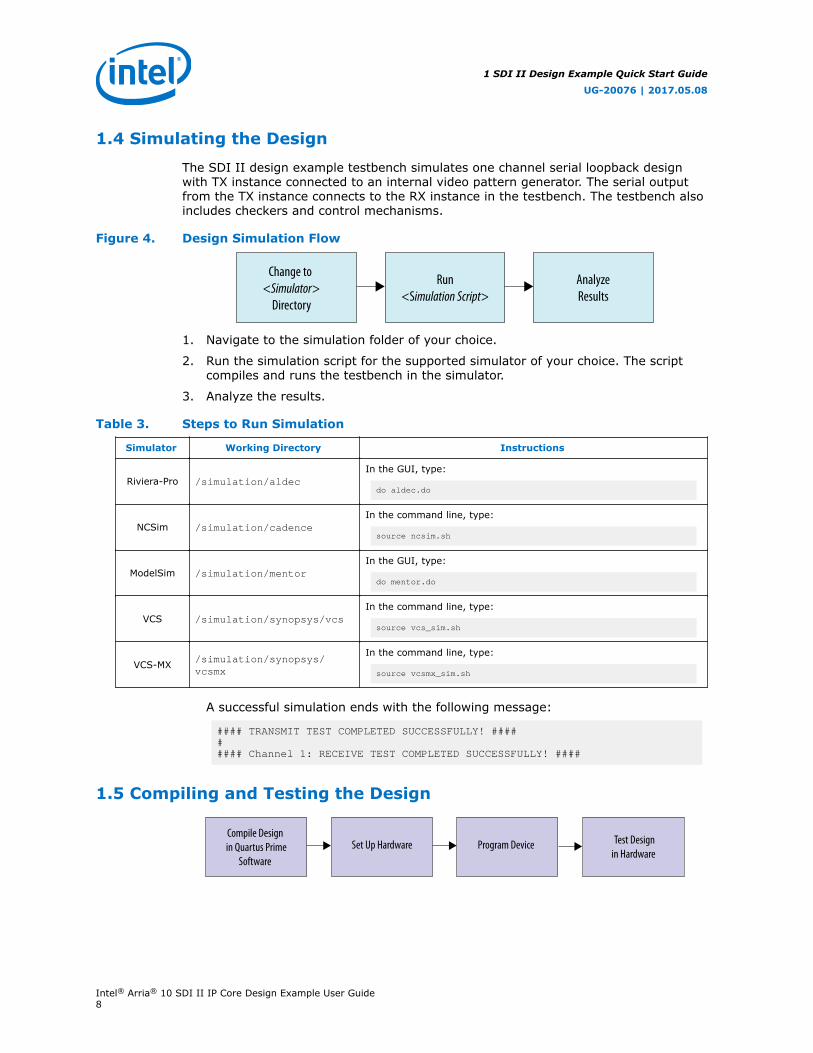
1.4 Simulating the Design
The SDI II design example testbench simulates one channel serial loopback designwith TX instance connected to an internal video pattern generator. The serial outputfrom the TX instance connects to the RX instance in the testbench. The testbench alsoincludes checkers and control mechanisms.
Figure 4. Design Simulation Flow
Change to <Simulator>
Directory
Run<Simulation Script>
AnalyzeResults
1. Navigate to the simulation folder of your choice.
2. Run the simulation script for the supported simulator of your choice. The scriptcompiles and runs the testbench in the simulator.
3. Analyze the results.
Table 3. Steps to Run Simulation
Simulator Working Directory Instructions
Riviera-Pro /simulation/aldecIn the GUI, type:
do aldec.do
NCSim /simulation/cadenceIn the command line, type:
source ncsim.sh
ModelSim /simulation/mentorIn the GUI, type:
do mentor.do
VCS /simulation/synopsys/vcsIn the command line, type:
source vcs_sim.sh
VCS-MX /simulation/synopsys/vcsmx
In the command line, type:
source vcsmx_sim.sh
A successful simulation ends with the following message:
#### TRANSMIT TEST COMPLETED SUCCESSFULLY! ##### #### Channel 1: RECEIVE TEST COMPLETED SUCCESSFULLY! ####
1.5 Compiling and Testing the Design
Compile Design in Quartus Prime
SoftwareSet Up Hardware Program Device Test Design
in Hardware
1 SDI II Design Example Quick Start Guide
UG-20076 | 2017.05.08
Intel® Arria® 10 SDI II IP Core Design Example User Guide8

To compile and run a demonstration test on the hardware design example, followthese steps:
1. Ensure that the hardware design example generation is complete.
2. Open quartus/sdi_ii_a10_demo.qpf.
3. Click Processing ➤ Start Compilation.
4. If you turn on the Dynamic Tx clock switching parameter in the DesignExample parameter editor, set the frequency for CLK2 or CLK3 in the Si5338(U14) tab of the Clock Control GUI.
• For HD/3G-SDI single-rate and triple-rate designs, set CLK3 to 148.3516 MHz.
• For multi-rate designs, set CLK2 to 296.7033 MHz.
5. After successful compilation, the Quartus Prime software generates a .sof file inyour specified directory.
6. Configure the selected Arria 10 device on the development board using thegenerated .sof file (Tools ➤ Programmer ).
7. For serial loopback designs, open the System Console to control the internal videopattern generator. Click Tools ➤ System Debugging Tools ➤ System Console.
Note: Close the Clock Control GUI and the Programmer window before you openthe System Console.
8. After the initialization, type source ../hwtest/tpg_ctrl.tcl in the SystemConsole to open the pattern generator control user interface. Select your desiredvideo format.
Related Links
Setting Up Environment VariablesProvides information about setting up the Clock Control application.
1.5.1 Connection and Settings Guidelines
Before programing with the .sof file, ensure that the connections and settings arecorrect.
Connections and Settings for HD/3G-SDI Single Rate and Triple Rate Designs
• For parallel loopback design, the on-board SMB RX connector (J20) connects to anexternal video source and the on-board SMB TX connector (J21) connects to avideo analyzer.
• For serial loopback design, the on-board SMB TX connector (J21) connects to anon-board SMB RX connector (J20) or a video analyzer.
• Ensure all switches on the development board are in default position.
• The SDI video analyzer displays the video generated from the source.
Note: For parallel loopback designs, you may need to switch the Si516_FS(SW6.3) at the back of the board if you are switching between fractionalframe rate and integer frame rate video format.
1 SDI II Design Example Quick Start Guide
UG-20076 | 2017.05.08
Intel® Arria® 10 SDI II IP Core Design Example User Guide9

Figure 5. Switch Settings on the Arria 10 Development Board
SW5
ON12
34
MSEL0MSEL1MSEL2VIDEN
SW4
CLK_SELCLK_ENSi516_FSFACTORYRZQ_B2K
ON1
1 0 1 0
23
4
ARRIA 10MAX VFMCAFMCB
SW6
ON12
34
5Table 4. SW6 DIP Switch Default Settings (Board Button)
Switch Board Label Description
1 CLK_SEL • ON for 100 MHz on-board clock oscillator selection (Defaultposition)
• OFF for SMA input clock selection
2 CLK_EN OFF for setting CLK_ENABLE high to the MAX V
3 SI516_FS • ON for setting the SDI REFCLK frequency to 148.35 MHz• OFF for setting the SDI REFCLK frequency to 148.5 MHz (Default
position)
4 FACTORY • ON to load factory from flash (Default position)• OFF to load user hardware from flash
5 RZQ_B2K • ON for setting RZQ resistor of Bank 2K to 99.17 ohm• OFF for setting RZQ resistor of Bank 2K to 240 ohm (Default
position)
1 SDI II Design Example Quick Start Guide
UG-20076 | 2017.05.08
Intel® Arria® 10 SDI II IP Core Design Example User Guide10

Connections and Settings for Multi Rate Design
• A VIDIO™ FMC Development Module VIDIO-12G-A (Nextera 12G SDI FMCdaughter card) connects to the FMC Port B on the development board.
• For parallel loopback design, the BNC RX connector (J1/12G In) connects to anexternal video source and the TX connector (J2/12G Out) connects to a videoanalyzer.
• For serial loopback design, the BNC TX connector (J2/12G Out) connects to theBNC RX connector (J1/12G In) or a video analyzer.
• Ensure all switches on the development board are in default position.
• The SDI video analyzer displays the video generated from the source.
Note: Change the jumper (J8) position before switching between fractional framerate and integer frame rate video formats. Press the push button (PB0) totrigger a device (LMK03328) power cycling through the PDN pin every timeyou change the jumper (J8) position.
Figure 6. Jumper Settings on Nextera 12G-SDI FMC Daughter CardRefer to these settings to change the jumper (J8) position.
Pin 2 - 3296.7 MHz
OpenPin 1 - 2SDI Mode
Table 5. Jumper Settings
Jumper Block Description
J7 Programming header
J8 To switch the generated clock frequency for the TX channel:• Pin 1–2 = 297 MHz• Pin 2–3 = 297/1.001 MHz
J9 To select SDI or IP mode:• Pin 1–2 = SDI mode• Pin 2–3 = IP mode
Related Links
Intel Arria 10 FPGA Development Kit User Guide
1.5.2 Design Limitations for Serial Loopback Design
The serial loopback design example has the following limitations:
1 SDI II Design Example Quick Start Guide
UG-20076 | 2017.05.08
Intel® Arria® 10 SDI II IP Core Design Example User Guide11
• You may encounter certain problems with the 12G-SDI 2160p59.94 in the serialloopback design that cannot be detected on the Omnitek Ultra 4K analyzer(software v2.1).
• Serial loopback design is mainly for image and TX clock switching demonstrationsonly. To get a more accurate jitter performance with the daughter cardcomponents, use the parallel loopback design and connect it to a clean videosource.
• To allow segmented frame video format (1080sF30, 1080sF25) and interlacedvideo format (1080i60, 1080i50) to be correctly differentiated in the externalanalyzer, Payload ID has to be inserted in the serial loopback design.
1 SDI II Design Example Quick Start Guide
UG-20076 | 2017.05.08
Intel® Arria® 10 SDI II IP Core Design Example User Guide12

2 SDI II Design Example Detailed DescriptionThe SDI II IP core includes three design examples for Arria 10 devices.
• Parallel loopback with external VCXO
• Parallel loopback without external VCXO
• Serial loopback
Features
• For HD/3G-SDI single rate and triple rate designs, you can choose either CMU orfPLL as the TX PLL.
• All designs use LED status for early debugging stage.
• The simplex serial loopback designs include RX and TX options. To use RX or TXonly components, remove the irrelevant blocks from the designs.
User Requirement Preserve Remove
RX Only RX Top — TX Top— Transceiver Arbiter
TX Only TX Top — RX Top— Transceiver Arbiter
Note: You can directly connect the Avalon-MM pins at the RX or TX Top as shownin the diagram below.
UG-20076 | 2017.05.08
Intel Corporation. All rights reserved. Intel, the Intel logo, Altera, Arria, Cyclone, Enpirion, MAX, Nios, Quartusand Stratix words and logos are trademarks of Intel Corporation or its subsidiaries in the U.S. and/or othercountries. Intel warrants performance of its FPGA and semiconductor products to current specifications inaccordance with Intel's standard warranty, but reserves the right to make changes to any products and servicesat any time without notice. Intel assumes no responsibility or liability arising out of the application or use of anyinformation, product, or service described herein except as expressly agreed to in writing by Intel. Intelcustomers are advised to obtain the latest version of device specifications before relying on any publishedinformation and before placing orders for products or services.*Other names and brands may be claimed as the property of others.
ISO9001:2008Registered

Figure 7. Components Required for TX or RX Only Design
TopRX Top
SDI IIRX
TransceiverPHY Reset
Controller (RX)
TransceiverNative PHY
(RX)
RXReconfiguration
ManagementTransceiver
Arbiter
Pattern Generator Control
SDI RX System
TX Top
SDI IITX
TransceiverPHY Reset
C ontroller (RT)
TransceiverNative PHY
(TX)
SDI TX System
TXPLLAlt
Pattern GeneratorControl PIO
Parallel DataSerial Data
Control/StatusAvalon-MM
JTAG to AvalonMaster Bridge
Video PatternGenerator
TXPLL
TXReconfiguration
Management
TX Only ComponentsRX Only ComponentsRemoved Blocks
2.1 Parallel Loopback Design Examples
The parallel loopback design examples demonstrate simplex and duplex channelmodes with and without external VCXO.
Note: For parallel loopback duplex designs, do not share the TX PLL reference clock with theRX transceiver reference clock. The design logic tunes the TX PLL clock to match theRX recovered clock frequency. For the parallel loopback with external VCXO designs(single-rate and triple-rate), use the only 148.5 MHz on-board oscillator as the TX PLLreference clock. For the RX reference clock, use a 270 MHz clock from another on-board oscillator.
2 SDI II Design Example Detailed Description
UG-20076 | 2017.05.08
Intel® Arria® 10 SDI II IP Core Design Example User Guide14

Parallel Loopback with Simplex Mode
Figure 8. Parallel Loopback with Simplex Mode Block Diagram
TopRX Top
SDI IIRX
TransceiverPHY Reset
Controller (RX)
TransceiverNative PHY
(RX)
RXReconfigurationManagement (3)
TransceiverArbiter (3)
Loopback TopSDI RX System
TX Top
SDI IITX
TransceiverPHY Reset
Controller (TX)
TransceiverNative PHY
(TX)
SDI TX System
TX PLL
LoopbackFIFO
PFD (1)
Reclock (2)
(4)
Parallel DataSerial Data
Control/StatusAvalon-MM
(1) Generate up/down control signal to on-board Si516 for clock synchronization purpose.(2) Block/Connection only required for parallel loopback without external VCXO designs.(3) Block/Connection only required for triple-rate/multi-rate designs.(4) FVH video sync signals to LMH1983 for clock synchronization purpose.
2 SDI II Design Example Detailed Description
UG-20076 | 2017.05.08
Intel® Arria® 10 SDI II IP Core Design Example User Guide15

Figure 9. Parallel Loopback with Simplex Mode Clocking Scheme
TopRX Top
SDI IIRX
TransceiverPHY Reset
Controller (RX)
TransceiverNative PHY
(RX)
RXReconfigurationManagement (3)
TransceiverArbiter
Loopback TopSDI RX System
TX Top
SDI IITX
TransceiverPHY Reset
Controller (TX)
TransceiverNative PHY
(TX)
SDI TX System
TX PLL
LoopbackFIFO
PFD (1)
Reclock (2)
TX PLL Reference ClockTX Transceiver clkoutTX PLL Serial ClockRX Reference ClockRX Transceiver clkoutManagement Clock
RX ReferenceClock
ManagementClock
TX PLLReference
Clock(1) Block/Connection only required for parallel loopback with external VCXO designs.(2) Block/Connection only required for parallel loopback without external VCXO designs.(3) Block/Connection only required for triple-rate/multi-rate designs.
2 SDI II Design Example Detailed Description
UG-20076 | 2017.05.08
Intel® Arria® 10 SDI II IP Core Design Example User Guide16

Parallel Loopback with Duplex Mode
Figure 10. Parallel Loopback with Duplex Mode Block Diagram
TopDuplex Top
SDI IIDuplex
TransceiverPHY Reset
Controller (RX)
TransceiverNative PHY
(Duplex)
RXReconfigurationManagement (3)
TransceiverArbiter (3)
Loopback TopSDI Duplex System
TX PLL
LoopbackFIFO
PFD (1)
Reclock (2)
Parallel DataSerial Data
Control/StatusAvalon-MM
(4)
TransceiverPHY Reset
C ontroller (TX)
(1) Generate up/down control signal to on-board Si516 for clock synchronization purpose.(2) Block/Connection only required for parallel loopback without external VCXO designs.(3) Block/Connection only required for triple-rate/multi-rate designs.(4) FVH video sync signals to LMH1983 for clock synchronization purpose.
2 SDI II Design Example Detailed Description
UG-20076 | 2017.05.08
Intel® Arria® 10 SDI II IP Core Design Example User Guide17

Figure 11. Parallel Loopback with Duplex Mode Clocking Scheme
TopDuplex Top
SDI IIDuplex
TransceiverPHY Reset
Controller (RX)
TransceiverNative PHY
(Duplex)
RXReconfigurationManagement (3)
TransceiverArbiter (3)
Loopback TopSDI Duplex System
TX PLL
LoopbackFIFO
PFD (1)
Reclock (2)TransceiverPHY Reset
Controller (TX)
TX PLL Reference ClockTX Transceiver clkoutTX PLL Serial ClockRX Reference ClockRX Transceiver clkoutManagement Clock
RX ReferenceClock
ManagementClock
TX PLLReference
Clock
(1) Block/Connection only required for parallel loopback with external VCXO designs.(2) Block/Connection only required for parallel loopback without external VCXO designs.(3) Block/Connection only required for triple-rate/multi-rate designs.
2.2 Serial Loopback Design Examples
The serial loopback design examples demonstrate simplex and duplex channel modes.
2 SDI II Design Example Detailed Description
UG-20076 | 2017.05.08
Intel® Arria® 10 SDI II IP Core Design Example User Guide18
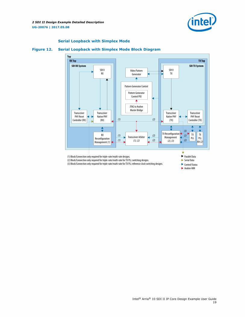
Serial Loopback with Simplex Mode
Figure 12. Serial Loopback with Simplex Mode Block Diagram
TopRX Top
SDI IIRX
TransceiverPHY Reset
Controller (RX)
TransceiverNative PHY
(RX)
RXReconfigurationManagement (1)
Transceiver Arbiter(1), (2)
Pattern Generator Control
SDI RX System
TX Top
SDI IITX
TransceiverPHY Reset
Controller (TX)
TransceiverNative PHY
(TX)
SDI TX System
TXPLL
Alt (2)
Pattern GeneratorControl PIO
Parallel DataSerial Data
Control/StatusAvalon-MM
(1) Block/Connection only required for triple-rate/multi-rate designs.(2) Block/Connection only required for triple-rate/multi-rate for TX PLL switching designs.(3) Block/Connection only required for triple-rate/multi-rate for TX PLL reference clock switching designs.
JTAG to AvalonMaster Bridge
Video PatternGenerator
(1) (2)
(1)
(1)
TXPLL
TX ReconfigurationManagement
(2), (3)
(2)
(2)
(2)
(2)
(3)
2 SDI II Design Example Detailed Description
UG-20076 | 2017.05.08
Intel® Arria® 10 SDI II IP Core Design Example User Guide19
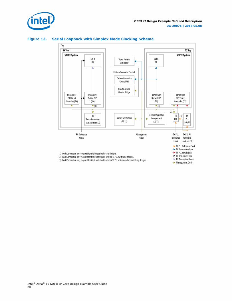
Figure 13. Serial Loopback with Simplex Mode Clocking Scheme
Top
RX Top
SDI IIRX
TransceiverPHY Reset
Controller (RX)
TransceiverNative PHY
(RX)
RXReconfigurationManagement (1)
Transceiver Arbiter(1), (2)
Pattern Generator Control
SDI RX System
TX Top
SDI IITX
TransceiverPHY Reset
Controller (TX)
TransceiverNative PHY
(TX)
SDI TX System
TXPLL
Alt (2)
Pattern GeneratorControl PIO
JTAG to AvalonMaster Bridge
Video PatternGenerator
TXPLL
TX ReconfigurationManagement
(2), (3)
TX PLL Reference ClockTX Transceiver clkoutTX PLL Serial ClockRX Reference ClockRX Transceiver clkoutManagement Clock
(1) Block/Connection only required for triple-rate/multi-rate designs.(2) Block/Connection only required for triple-rate/multi-rate for TX PLL switching designs. (3) Block/Connection only required for triple-rate/multi-rate for TX PLL reference clock switching designs.
ManagementClock
RX ReferenceClock
TX PLL AltReference
Clock (2), (3)
TX PLLReference
Clock
(1) (2)
(3)
(3)
2 SDI II Design Example Detailed Description
UG-20076 | 2017.05.08
Intel® Arria® 10 SDI II IP Core Design Example User Guide20

Serial Loopback with Duplex Mode
Figure 14. Serial Loopback with Duplex Mode Block Diagram
TopDuplex Top
SDI IIDuplex
TransceiverPHY Reset
Controller (RX)
TransceiverNative PHY
(Duplex)
RXReconfigurationManagement (1) Transceiver Arbiter
(1), (2)
Pattern Generator Control
SDI Duplex System
Pattern GeneratorControl PIO
Parallel DataSerial Data
Control/StatusAvalon-MM
(1) Block/Connection only required for triple-rate/multi-rate designs.(2) Block/Connection only required for triple-rate/multi-rate for TX PLL switching designs.(3) Block/Connection only required for triple-rate/multi-rate for TX PLL reference clock switching designs.
JTAG to AvalonMaster Bridge
Video PatternGenerator
TransceiverPHY Reset
Controller (TX)
TXPLL
Alt (2)
TXPLL
TX ReconfigurationManagement
(2), (3)
(2)
(2)
(3)
2 SDI II Design Example Detailed Description
UG-20076 | 2017.05.08
Intel® Arria® 10 SDI II IP Core Design Example User Guide21

Figure 15. Serial Loopback with Duplex Mode Clocking Scheme
TopDuplex Top
SDI IIDuplex
TransceiverPHY Reset
Controller (RX)
TransceiverNative PHY
(Duplex)
RXReconfigurationManagement (1) Transceiver Arbiter
(1), (2)
Pattern Generator Control
SDI Duplex System
Pattern GeneratorControl PIO
JTAG to AvalonMaster Bridge
Video PatternGenerator
TransceiverPHY Reset
Controller (TX)
TXPLL
Alt (2)
TXPLL
TX ReconfigurationManagement
(2), (3)
(2)
(3)
(3)
TX PLL Reference ClockTX Transceiver clkoutTX PLL Serial ClockRX Reference ClockRX Transceiver clkoutManagement Clock
TX PLL AltReference
Clock (2), (3)
TX PLLReference
Clock
RXReference
Clock
ManagementClock
(1) Block/Connection only required for triple-rate/multi-rate designs.(2) Block/Connection only required for triple-rate/multi-rate for TX PLL switching designs. (3) Block/Connection only required for triple-rate/multi-rate for TX PLL reference clock switching designs.
2.3 Design Components
The SDI II IP core design examples require the following components.
2 SDI II Design Example Detailed Description
UG-20076 | 2017.05.08
Intel® Arria® 10 SDI II IP Core Design Example User Guide22
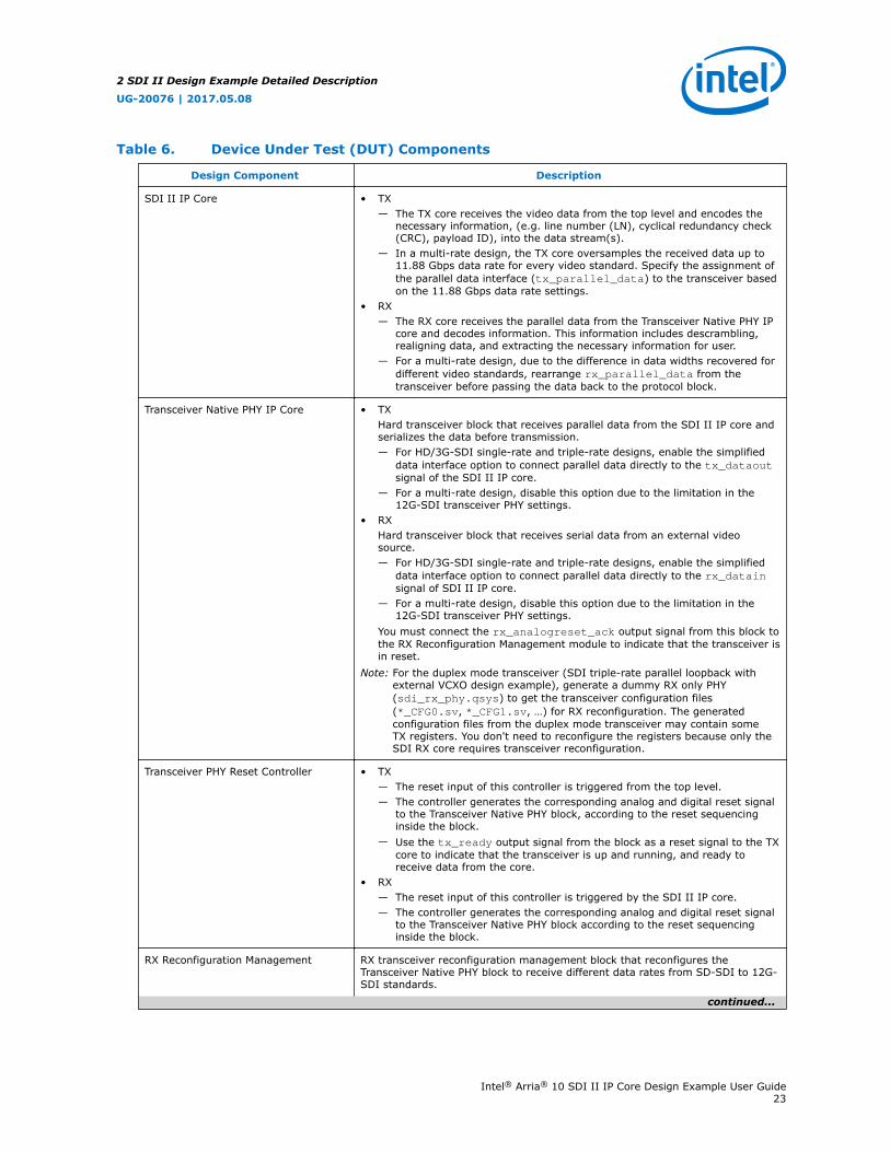
Table 6. Device Under Test (DUT) Components
Design Component Description
SDI II IP Core • TX— The TX core receives the video data from the top level and encodes the
necessary information, (e.g. line number (LN), cyclical redundancy check(CRC), payload ID), into the data stream(s).
— In a multi-rate design, the TX core oversamples the received data up to11.88 Gbps data rate for every video standard. Specify the assignment ofthe parallel data interface (tx_parallel_data) to the transceiver basedon the 11.88 Gbps data rate settings.
• RX— The RX core receives the parallel data from the Transceiver Native PHY IP
core and decodes information. This information includes descrambling,realigning data, and extracting the necessary information for user.
— For a multi-rate design, due to the difference in data widths recovered fordifferent video standards, rearrange rx_parallel_data from thetransceiver before passing the data back to the protocol block.
Transceiver Native PHY IP Core • TXHard transceiver block that receives parallel data from the SDI II IP core andserializes the data before transmission.— For HD/3G-SDI single-rate and triple-rate designs, enable the simplified
data interface option to connect parallel data directly to the tx_dataoutsignal of the SDI II IP core.
— For a multi-rate design, disable this option due to the limitation in the12G-SDI transceiver PHY settings.
• RXHard transceiver block that receives serial data from an external videosource.— For HD/3G-SDI single-rate and triple-rate designs, enable the simplified
data interface option to connect parallel data directly to the rx_datainsignal of SDI II IP core.
— For a multi-rate design, disable this option due to the limitation in the12G-SDI transceiver PHY settings.
You must connect the rx_analogreset_ack output signal from this block tothe RX Reconfiguration Management module to indicate that the transceiver isin reset.
Note: For the duplex mode transceiver (SDI triple-rate parallel loopback withexternal VCXO design example), generate a dummy RX only PHY(sdi_rx_phy.qsys) to get the transceiver configuration files(*_CFG0.sv, *_CFG1.sv, …) for RX reconfiguration. The generatedconfiguration files from the duplex mode transceiver may contain someTX registers. You don't need to reconfigure the registers because only theSDI RX core requires transceiver reconfiguration.
Transceiver PHY Reset Controller • TX— The reset input of this controller is triggered from the top level.— The controller generates the corresponding analog and digital reset signal
to the Transceiver Native PHY block, according to the reset sequencinginside the block.
— Use the tx_ready output signal from the block as a reset signal to the TXcore to indicate that the transceiver is up and running, and ready toreceive data from the core.
• RX— The reset input of this controller is triggered by the SDI II IP core.— The controller generates the corresponding analog and digital reset signal
to the Transceiver Native PHY block according to the reset sequencinginside the block.
RX Reconfiguration Management RX transceiver reconfiguration management block that reconfigures theTransceiver Native PHY block to receive different data rates from SD-SDI to 12G-SDI standards.
continued...
2 SDI II Design Example Detailed Description
UG-20076 | 2017.05.08
Intel® Arria® 10 SDI II IP Core Design Example User Guide23
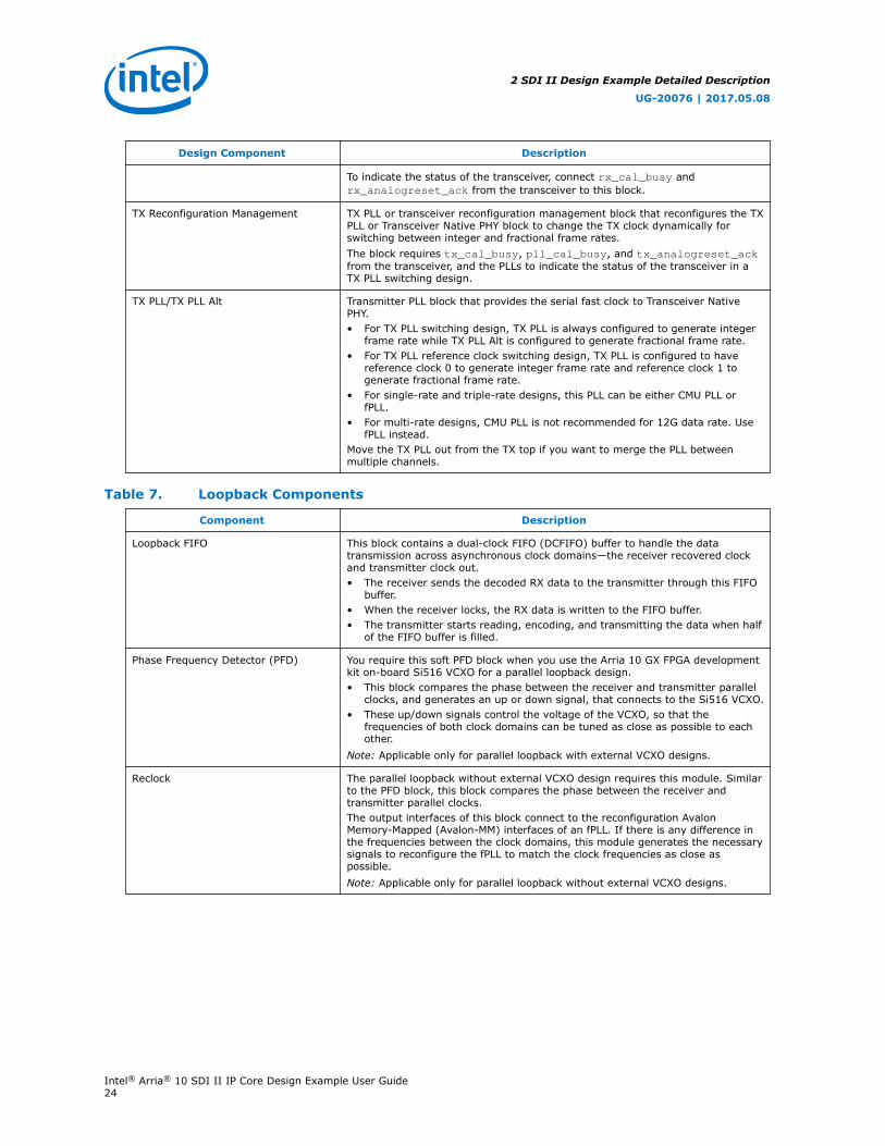
Design Component Description
To indicate the status of the transceiver, connect rx_cal_busy andrx_analogreset_ack from the transceiver to this block.
TX Reconfiguration Management TX PLL or transceiver reconfiguration management block that reconfigures the TXPLL or Transceiver Native PHY block to change the TX clock dynamically forswitching between integer and fractional frame rates.The block requires tx_cal_busy, pll_cal_busy, and tx_analogreset_ackfrom the transceiver, and the PLLs to indicate the status of the transceiver in aTX PLL switching design.
TX PLL/TX PLL Alt Transmitter PLL block that provides the serial fast clock to Transceiver NativePHY.• For TX PLL switching design, TX PLL is always configured to generate integer
frame rate while TX PLL Alt is configured to generate fractional frame rate.• For TX PLL reference clock switching design, TX PLL is configured to have
reference clock 0 to generate integer frame rate and reference clock 1 togenerate fractional frame rate.
• For single-rate and triple-rate designs, this PLL can be either CMU PLL orfPLL.
• For multi-rate designs, CMU PLL is not recommended for 12G data rate. UsefPLL instead.
Move the TX PLL out from the TX top if you want to merge the PLL betweenmultiple channels.
Table 7. Loopback Components
Component Description
Loopback FIFO This block contains a dual-clock FIFO (DCFIFO) buffer to handle the datatransmission across asynchronous clock domains—the receiver recovered clockand transmitter clock out.• The receiver sends the decoded RX data to the transmitter through this FIFO
buffer.• When the receiver locks, the RX data is written to the FIFO buffer.• The transmitter starts reading, encoding, and transmitting the data when half
of the FIFO buffer is filled.
Phase Frequency Detector (PFD) You require this soft PFD block when you use the Arria 10 GX FPGA developmentkit on-board Si516 VCXO for a parallel loopback design.• This block compares the phase between the receiver and transmitter parallel
clocks, and generates an up or down signal, that connects to the Si516 VCXO.• These up/down signals control the voltage of the VCXO, so that the
frequencies of both clock domains can be tuned as close as possible to eachother.
Note: Applicable only for parallel loopback with external VCXO designs.
Reclock The parallel loopback without external VCXO design requires this module. Similarto the PFD block, this block compares the phase between the receiver andtransmitter parallel clocks.The output interfaces of this block connect to the reconfiguration AvalonMemory-Mapped (Avalon-MM) interfaces of an fPLL. If there is any difference inthe frequencies between the clock domains, this module generates the necessarysignals to reconfigure the fPLL to match the clock frequencies as close aspossible.Note: Applicable only for parallel loopback without external VCXO designs.
2 SDI II Design Example Detailed Description
UG-20076 | 2017.05.08
Intel® Arria® 10 SDI II IP Core Design Example User Guide24
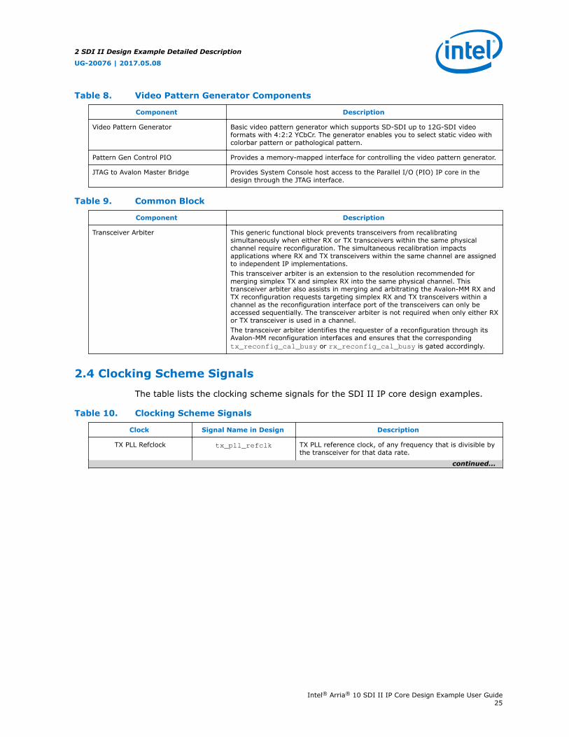
Table 8. Video Pattern Generator Components
Component Description
Video Pattern Generator Basic video pattern generator which supports SD-SDI up to 12G-SDI videoformats with 4:2:2 YCbCr. The generator enables you to select static video withcolorbar pattern or pathological pattern.
Pattern Gen Control PIO Provides a memory-mapped interface for controlling the video pattern generator.
JTAG to Avalon Master Bridge Provides System Console host access to the Parallel I/O (PIO) IP core in thedesign through the JTAG interface.
Table 9. Common Block
Component Description
Transceiver Arbiter This generic functional block prevents transceivers from recalibratingsimultaneously when either RX or TX transceivers within the same physicalchannel require reconfiguration. The simultaneous recalibration impactsapplications where RX and TX transceivers within the same channel are assignedto independent IP implementations.This transceiver arbiter is an extension to the resolution recommended formerging simplex TX and simplex RX into the same physical channel. Thistransceiver arbiter also assists in merging and arbitrating the Avalon-MM RX andTX reconfiguration requests targeting simplex RX and TX transceivers within achannel as the reconfiguration interface port of the transceivers can only beaccessed sequentially. The transceiver arbiter is not required when only either RXor TX transceiver is used in a channel.The transceiver arbiter identifies the requester of a reconfiguration through itsAvalon-MM reconfiguration interfaces and ensures that the correspondingtx_reconfig_cal_busy or rx_reconfig_cal_busy is gated accordingly.
2.4 Clocking Scheme Signals
The table lists the clocking scheme signals for the SDI II IP core design examples.
Table 10. Clocking Scheme Signals
Clock Signal Name in Design Description
TX PLL Refclock tx_pll_refclk TX PLL reference clock, of any frequency that is divisible bythe transceiver for that data rate.
continued...
2 SDI II Design Example Detailed Description
UG-20076 | 2017.05.08
Intel® Arria® 10 SDI II IP Core Design Example User Guide25

Clock Signal Name in Design Description
Note: You must connect this clock to a dedicatedtransceiver reference clock pin.
• Parallel loopback with external VCXO— Use a minimum clock frequency of 148.5 MHz
(single-rate/triple-rate) or 297 MHz (multi-rate) tomeet jitter performance specification.
— Using a higher clock frequency would require amodification of the TX PLL reference clock value inthe TX PLL parameter editor.
• Parallel loopback without external VCXO— The recommended frequency is 100 MHz.
• Serial loopback— For this design, the TX PLL refclock is configured to
generate clock for integer frame rate.— The minimum clock frequency is 148.5 MHz (single-
rate/triple-rate) or 297 MHz (multi-rate) to meetjitter performance specification.
— Using a higher clock frequency would require amodification of the TX PLL reference clock value in TXPLL parameter editor.
TX PLL Alt Refclock tx_pll_refclk_alt Second TX PLL reference clock which can be any clockfrequency that is divisible by transceiver for that data rate.This clock must be connected to a dedicated transceiverreference clock pin.• Serial loopback
— For this design example, TX PLL alt refclock isconfigured to generate clock for fractional frame rate.
— The minimum clock frequency is 148.35 MHz (single-rate/triple-rate) or 297.7 MHz (multi-rate) to meetjitter performance specification.
— Using a higher clock frequency would require amodification of the TX PLL reference clock value inthe TX PLL parameter editor.
TX Transceiver Clockout tx_vid_clkout Recovered clock from the transceiver.• HD-SDI single rate
— 74.25 MHz (default)— 74.1758 MHz (for the Dynamic TX clock switching
feature when you transmit video format withfractional frame rate)
• 3G-SDI single rate, triple rate or multi rate— 148.5 MHz (default)— 148.35 MHz (for the Dynamic TX clock switching
feature when you transmit video format withfractional frame rate)
TX PLL Serial Clock tx_serial_clk Serial fast clock generated by TX PLL. The clock frequency isset based on the data rate.
RX Refclock rx_cdr_refclk Transceiver clock data recovery (CDR) reference clock, ofany frequency that is divisible by the transceiver for thatdata rate. Only a single reference clock frequency isrequired to support both integer and fractional frame rates.It must be a free running clock connected to the transceiverclock pin.
continued...
2 SDI II Design Example Detailed Description
UG-20076 | 2017.05.08
Intel® Arria® 10 SDI II IP Core Design Example User Guide26

Clock Signal Name in Design Description
• Parallel loopback with external VCXO— For this design example, the minimum clock
frequency of 148.5 MHz is used in the multi-ratedesign example. For single-rate and triple-rate designexamples, a higher reference clock (270 MHz) is usedinstead.
— Using a higher clock frequency would require amodification of the RX CDR reference clock value inthe Arria 10 Native PHY Transceiver parameter editor.For triple or multi-rate modes, you need to modifythe reference clock value for every profiles.
• Parallel loopback without external VCXO and Serialloopback— The minimum clock frequency is 148.5 MHz.— Using a higher clock frequency would require a
modification of the RX CDR reference clock value inthe Arria 10 Native PHY Transceiver parameter editor.For triple or multi-rate modes, you need to modifythe reference clock value for every profiles.
Note: Do not share the TX PLL reference clock with the RXtransceiver reference clock for a parallel loopbackdesign. In parallel loopback designs, the TX PLLclock is tuned to match the RX recovered clockfrequency.
rx_core_refclk SDI RX core reference clock.The required frequency is 148.5 MHz. This clock must be afree-running clock.
continued...
2 SDI II Design Example Detailed Description
UG-20076 | 2017.05.08
Intel® Arria® 10 SDI II IP Core Design Example User Guide27
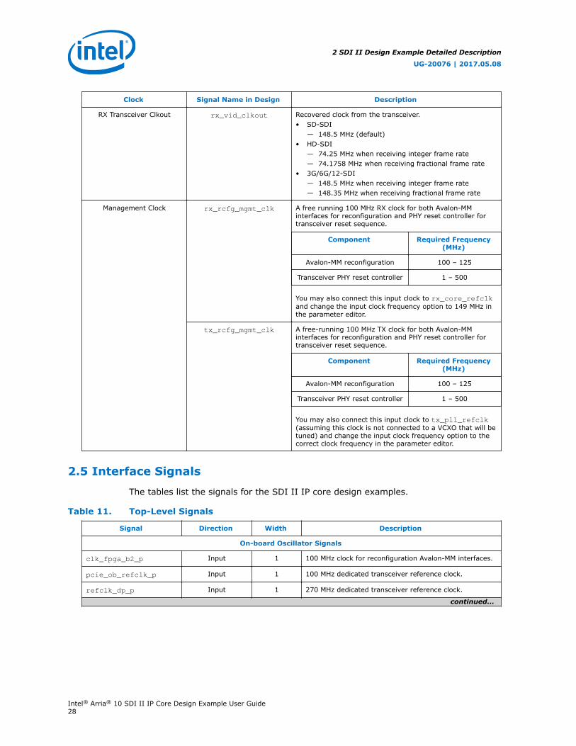
Clock Signal Name in Design Description
RX Transceiver Clkout rx_vid_clkout Recovered clock from the transceiver.• SD-SDI
— 148.5 MHz (default)• HD-SDI
— 74.25 MHz when receiving integer frame rate— 74.1758 MHz when receiving fractional frame rate
• 3G/6G/12-SDI— 148.5 MHz when receiving integer frame rate— 148.35 MHz when receiving fractional frame rate
Management Clock rx_rcfg_mgmt_clk A free running 100 MHz RX clock for both Avalon-MMinterfaces for reconfiguration and PHY reset controller fortransceiver reset sequence.
Component Required Frequency(MHz)
Avalon-MM reconfiguration 100 – 125
Transceiver PHY reset controller 1 – 500
You may also connect this input clock to rx_core_refclkand change the input clock frequency option to 149 MHz inthe parameter editor.
tx_rcfg_mgmt_clk A free-running 100 MHz TX clock for both Avalon-MMinterfaces for reconfiguration and PHY reset controller fortransceiver reset sequence.
Component Required Frequency(MHz)
Avalon-MM reconfiguration 100 – 125
Transceiver PHY reset controller 1 – 500
You may also connect this input clock to tx_pll_refclk(assuming this clock is not connected to a VCXO that will betuned) and change the input clock frequency option to thecorrect clock frequency in the parameter editor.
2.5 Interface Signals
The tables list the signals for the SDI II IP core design examples.
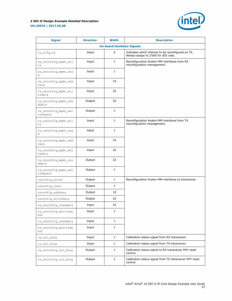
Table 11. Top-Level Signals
Signal Direction Width Description
On-board Oscillator Signals
clk_fpga_b2_p Input 1 100 MHz clock for reconfiguration Avalon-MM interfaces.
pcie_ob_refclk_p Input 1 100 MHz dedicated transceiver reference clock.
refclk_dp_p Input 1 270 MHz dedicated transceiver reference clock.
continued...
2 SDI II Design Example Detailed Description
UG-20076 | 2017.05.08
Intel® Arria® 10 SDI II IP Core Design Example User Guide28

Signal Direction Width Description
On-board Oscillator Signals
refclk_sdi_p Input 1 148.5 or 148.35 MHz dedicated transceiver referenceclock.
refclk_sma_p Input 1 302 MHz dedicated transceiver reference clock.Programmable to 148.3516 MHz from the Clock ControlGUI.
refclk_fmcb_p Input 1 625 MHz dedicated transceiver reference clock.Programmable to 296.7033 MHz from the Clock ControlGUI.
User Push Buttons and LEDs
user_pb0 Input 1 Push button to power down LMK03328 after switchingthe jumper settings.
cpu_resetn Input 1 Global reset.
user_led_g Output 8 Green LED display.
user_led_r Output 8 Red LED display.
On-board Si516, SDI Cable Driver and Equalizer Related Pins
sdi_rx_p Input 1 On-board SDI RX serial data.
sdi_tx_p Output 1 On-board SDI TX serial data.
sdi_clk148_up Output 1 Voltage control for Si516.
sdi_clk148_down Output 1 Voltage control for Si516.
sdi_mf0_bypass Output 1 On-board SDI RX Equalizer Bypass.
sdi_mf1_auto_sleep Output 1 On-board SDI RX Equalizer Auto Sleep.
sdi_mf1_mute Output 1 On-board SDI RX Equalizer Mute.
sdi_tx_sd_hdn Output 1 On-board SDI TX cable driver slew rate control.
Nextera SDI FMC Daughter Card Pins on FMC Port B
fmcb_gbtclk_m2c_p0 Input 1 297 or 296.7 MHz dedicated transceiver reference clockfrom FMC port B.
fmcb_dp_m2c_p2 Input 1 SDI RX serial data from FMC port B.
fmcb_la_tx_p1 Input 1 RX cable equalizer lock status on Nextera daughter card.
fmcb_dp_c2m_p0 Output 1 SDI TX serial data from FMC port B.
fmcb_la_tx_p12 Output 1 Initialize LMH1983 on Nextera daughter card.
fmcb_la_tx_n12 Output 1 F sync signal LMH1983 on Nextera daughter card.
fmcb_la_tx_p14 Output 1 V sync signal LMH1983 on Nextera daughter card.
fmcb_la_tx_n14 Output 1 H sync signal LMH1983 on Nextera daughter card.
fmcb_la_tx_p15 Output 1 Power-down signal LMH1983 on Nextera daughter card.
2 SDI II Design Example Detailed Description
UG-20076 | 2017.05.08
Intel® Arria® 10 SDI II IP Core Design Example User Guide29
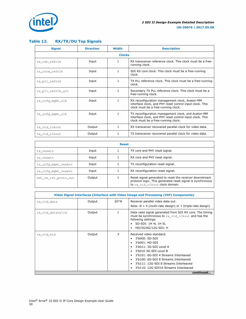
Table 12. RX/TX/DU Top Signals
Signal Direction Width Description
Clocks
rx_cdr_refclk Input 1 RX transceiver reference clock. This clock must be a free-running clock.
rx_core_refclk Input 1 SDI RX core clock. This clock must be a free-runningclock.
tx_pll_refclk Input 1 TX PLL reference clock. This clock must be a free-runningclock.
tx_pll_refclk_alt Input 1 Secondary TX PLL reference clock. This clock must be afree-running clock.
rx_rcfg_mgmt_clk Input 1 RX reconfiguration management clock, Avalon-MMinterface clock, and PHY reset control input clock. Thisclock must be a free-running clock.
tx_rcfg_mgmt_clk Input 1 TX reconfiguration management clock, and Avalon-MMinterface clock, and PHY reset control input clock. Thisclock must be a free-running clock.
rx_vid_clkout Output 1 RX transceiver recovered parallel clock for video data.
tx_vid_clkout Output 1 TX transceiver recovered parallel clock for video data.
Reset
tx_resetn Input 1 TX core and PHY reset signal.
rx_resetn Input 1 RX core and PHY reset signal.
tx_rcfg_mgmt_resetn Input 1 TX reconfiguration reset signal.
rx_rcfg_mgmt_resetn Input 1 RX reconfiguration reset signal.
sdi_rx_rst_proto_out Output 1 Reset signal generated to reset the receiver downstreamprotocol logic. This generated reset signal is synchronousto rx_vid_clkout clock domain.
Video Signal Interfaces (Interface with Video Image and Processing (VIP) Components)
rx_vid_data Output 20*N Receiver parallel video data out.Note: N = 4 (multi-rate design) or 1 (triple-rate design)
rx_vid_datavalid Output 1 Data valid signal generated from SDI RX core. The timingmust be synchronous to rx_vid_clkout and has thefollowing settings:• SD-SDI: 1H 4L 1H 5L• HD/3G/6G/12G-SDI: H
rx_vid_std Output 3 Received video standard.• 3'b000: SD-SDI• 3'b001: HD-SDI• 3'b011: 3G-SDI Level A• 3'b010 3G-SDI Level B• 3'b101: 6G-SDI 4 Streams Interleaved• 3'b100: 6G-SDI 8 Streams Interleaved• 3'b111: 12G-SDI 8 Streams Interleaved• 3'b110: 12G-SDI16 Streams Interleaved
continued...
2 SDI II Design Example Detailed Description
UG-20076 | 2017.05.08
Intel® Arria® 10 SDI II IP Core Design Example User Guide30
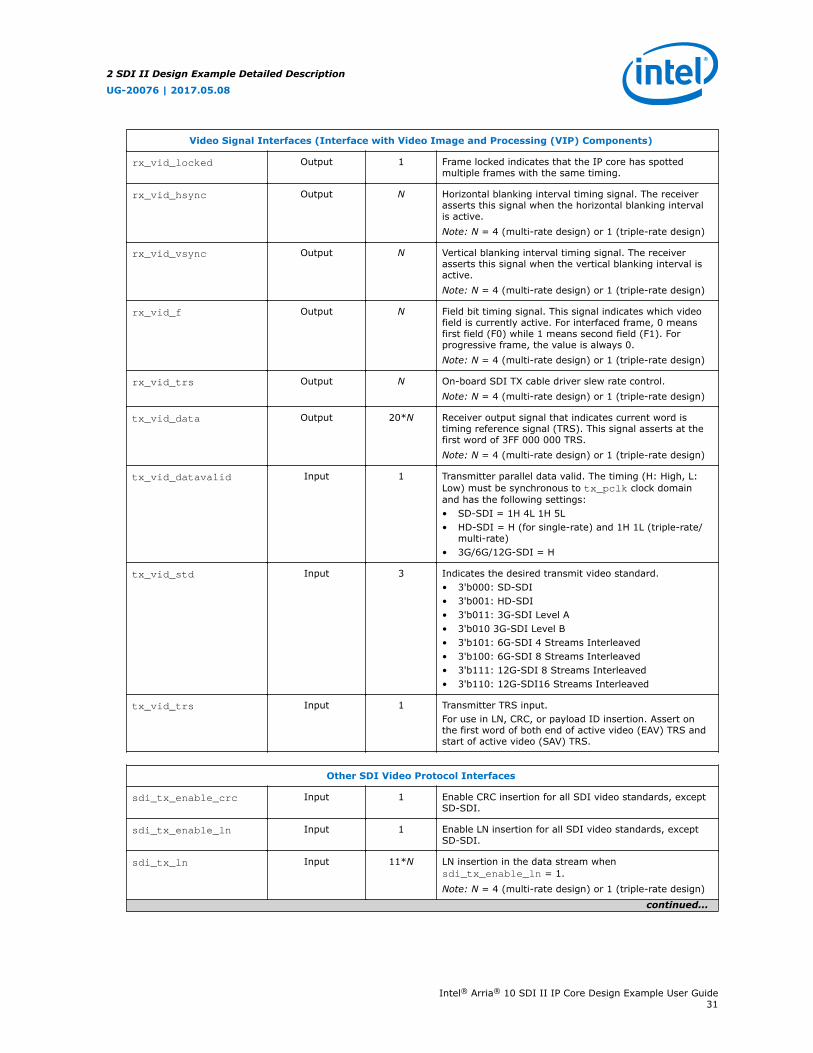
Video Signal Interfaces (Interface with Video Image and Processing (VIP) Components)
rx_vid_locked Output 1 Frame locked indicates that the IP core has spottedmultiple frames with the same timing.
rx_vid_hsync Output N Horizontal blanking interval timing signal. The receiverasserts this signal when the horizontal blanking intervalis active.Note: N = 4 (multi-rate design) or 1 (triple-rate design)
rx_vid_vsync Output N Vertical blanking interval timing signal. The receiverasserts this signal when the vertical blanking interval isactive.Note: N = 4 (multi-rate design) or 1 (triple-rate design)
rx_vid_f Output N Field bit timing signal. This signal indicates which videofield is currently active. For interfaced frame, 0 meansfirst field (F0) while 1 means second field (F1). Forprogressive frame, the value is always 0.Note: N = 4 (multi-rate design) or 1 (triple-rate design)
rx_vid_trs Output N On-board SDI TX cable driver slew rate control.Note: N = 4 (multi-rate design) or 1 (triple-rate design)
tx_vid_data Output 20*N Receiver output signal that indicates current word istiming reference signal (TRS). This signal asserts at thefirst word of 3FF 000 000 TRS.Note: N = 4 (multi-rate design) or 1 (triple-rate design)
tx_vid_datavalid Input 1 Transmitter parallel data valid. The timing (H: High, L:Low) must be synchronous to tx_pclk clock domainand has the following settings:• SD-SDI = 1H 4L 1H 5L• HD-SDI = H (for single-rate) and 1H 1L (triple-rate/
multi-rate)• 3G/6G/12G-SDI = H
tx_vid_std Input 3 Indicates the desired transmit video standard.• 3'b000: SD-SDI• 3'b001: HD-SDI• 3'b011: 3G-SDI Level A• 3'b010 3G-SDI Level B• 3'b101: 6G-SDI 4 Streams Interleaved• 3'b100: 6G-SDI 8 Streams Interleaved• 3'b111: 12G-SDI 8 Streams Interleaved• 3'b110: 12G-SDI16 Streams Interleaved
tx_vid_trs Input 1 Transmitter TRS input.For use in LN, CRC, or payload ID insertion. Assert onthe first word of both end of active video (EAV) TRS andstart of active video (SAV) TRS.
Other SDI Video Protocol Interfaces
sdi_tx_enable_crc Input 1 Enable CRC insertion for all SDI video standards, exceptSD-SDI.
sdi_tx_enable_ln Input 1 Enable LN insertion for all SDI video standards, exceptSD-SDI.
sdi_tx_ln Input 11*N LN insertion in the data stream whensdi_tx_enable_ln = 1.Note: N = 4 (multi-rate design) or 1 (triple-rate design)
continued...
2 SDI II Design Example Detailed Description
UG-20076 | 2017.05.08
Intel® Arria® 10 SDI II IP Core Design Example User Guide31
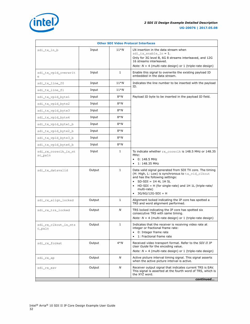
Other SDI Video Protocol Interfaces
sdi_tx_ln_b Input 11*N LN insertion in the data stream whensdi_tx_enable_ln = 1.Only for 3G level B, 6G 8 streams interleaved, and 12G16 streams interleaved.Note: N = 4 (multi-rate design) or 1 (triple-rate design)
sdi_tx_vpid_overwrite
Input 1 Enable this signal to overwrite the existing payload IDembedded in the data stream.
sdi_tx_line_f0 Input 11*N Indicates the line number to be inserted with the payloadID.
sdi_tx_line_f1 Input 11*N
sdi_tx_vpid_byte1 Input 8*N Payload ID byte to be inserted in the payload ID field.
sdi_tx_vpid_byte2 Input 8*N
sdi_tx_vpid_byte3 Input 8*N
sdi_tx_vpid_byte4 Input 8*N
sdi_tx_vpid_byte1_b Input 8*N
sdi_tx_vpid_byte2_b Input 8*N
sdi_tx_vpid_byte3_b Input 8*N
sdi_tx_vpid_byte4_b Input 8*N
sdi_rx_coreclk_is_ntsc_paln
Input 1 To indicate whether rx_coreclk is 148.5 MHz or 148.35MHz:• 0: 148.5 MHz• 1: 148.35 MHz
sdi_tx_datavalid Output 1 Data valid signal generated from SDI TX core. The timing(H: High, L: Low) is synchronous to tx_vid_clkoutand has the following settings:• SD-SDI = 1H 4L 1H 5L• HD-SDI = H (for single-rate) and 1H 1L (triple-rate/
multi-rate)• 3G/6G/12G-SDI = H
sdi_rx_align_locked Output 1 Alignment locked indicating the IP core has spotted aTRS and word alignment performed.
sdi_rx_trs_locked Output N TRS locked indicating the IP core has spotted sixconsecutive TRS with same timing.Note: N = 4 (multi-rate design) or 1 (triple-rate design)
sdi_rx_clkout_is_ntsc_paln
Output 1 Indicates that the receiver is receiving video rate atinteger or fractional frame rate:• 0: Integer frame rate• 1: Fractional frame rate
sdi_rx_format Output 4*N Received video transport format. Refer to the SDI II IPUser Guide for the encoding value.Note: N = 4 (multi-rate design) or 1 (triple-rate design)
sdi_rx_ap Output N Active picture interval timing signal. This signal assertswhen the active picture interval is active.
sdi_rx_eav Output N Receiver output signal that indicates current TRS is EAV.This signal is asserted at the fourth word of TRS, which isthe XYZ word.
continued...
2 SDI II Design Example Detailed Description
UG-20076 | 2017.05.08
Intel® Arria® 10 SDI II IP Core Design Example User Guide32

Other SDI Video Protocol Interfaces
sdi_rx_ln Output 11*N Received line number from protocol.
sdi_rx_ln_b Output 11*N
sdi_rx_crc_error_c Output N CRC error status signal from protocol.
sdi_rx_crc_error_y Output N
sdi_rx_crc_error_c_b Output N
sdi_rx_crc_error_y_b Output N
sdi_rx_line_f0 Output 11*N Payload ID status from protocol.
sdi_rx_line_f1 Output 11*N
sdi_rx_vpid_byte1 Output 8*N
sdi_rx_vpid_byte2 Output 8*N
sdi_rx_vpid_byte3 Output 8*N
sdi_rx_vpid_byte4 Output 8*N
sdi_rx_vpid_checksum_error
Output N
sdi_rx_vpid_valid Output N
sdi_rx_vpid_byte1_b Output 8*N
sdi_rx_vpid_byte2_b Output 8*N
sdi_rx_vpid_byte3_b Output 8*N
sdi_rx_vpid_byte4_b Output 8*N
sdi_rx_vpid_checksum_error_b
Output N
sdi_rx_vpid_valid_b Output N
Transceiver Interfaces
tx_pll_refclk_sel Input 1 Indicate which of pll_locked signals to be monitoredfor TX PHY reset controller's reset sequencing.Always set to 1'b0 if only one PLL is in use.
tx_rcfg_cal_busy Input 1 Transceiver calibration status to TX PHY reset controller.
rx_rcfg_cal_busy Input 1 Transceiver calibration status to RX PHY reset controllerand Rx reconfiguration management module.
gxb_rx_serial_data Input 1 RX transceiver serial data.
gxb_tx_serial_data Output 1 TX transceiver serial data.
gxb_rx_ready Output 1 RX transceiver status.
gxb_tx_ready Output 1 TX transceiver status.
gxb_rx_cal_busy Output 1 Calibration status signal from RX transceiver.
gxb_tx_cal_busy Output 1 Calibration status signal from TX transceiver.
tx_pll_locked Output 1 TX PLL lock status.
continued...
2 SDI II Design Example Detailed Description
UG-20076 | 2017.05.08
Intel® Arria® 10 SDI II IP Core Design Example User Guide33
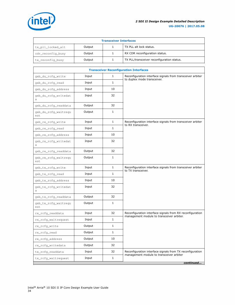
Transceiver Interfaces
tx_pll_locked_alt Output 1 TX PLL alt lock status.
cdr_reconfig_busy Output 1 RX CDR reconfiguration status.
tx_reconfig_busy Output 1 TX PLL/transceiver reconfiguration status.
Transceiver Reconfiguration Interfaces
gxb_du_rcfg_write Input 1 Reconfiguration interface signals from transceiver arbiterto duplex mode transceiver.
gxb_du_rcfg_read Input 1
gxb_du_rcfg_address Input 10
gxb_du_rcfg_writedata
Input 32
gxb_du_rcfg_readdata Output 32
gxb_du_rcfg_waitrequest
Output 1
gxb_rx_rcfg_write Input 1 Reconfiguration interface signals from transceiver arbiterto RX transceiver.
gxb_rx_rcfg_read Input 1
gxb_rx_rcfg_address Input 10
gxb_rx_rcfg_writedata
Input 32
gxb_rx_rcfg_readdata Output 32
gxb_rx_rcfg_waitrequest
Output 1
gxb_tx_rcfg_write Input 1 Reconfiguration interface signals from transceiver arbiterto TX transceiver.
gxb_tx_rcfg_read Input 1
gxb_tx_rcfg_address Input 10
gxb_tx_rcfg_writedata
Input 32
gxb_tx_rcfg_readdata Output 32
gxb_tx_rcfg_waitrequest
Output 1
rx_rcfg_readdata Input 32 Reconfiguration interface signals from RX reconfigurationmanagement module to transceiver arbiter.
rx_rcfg_waitrequest Input 1
rx_rcfg_write Output 1
rx_rcfg_read Output 1
rx_rcfg_address Output 10
rx_rcfg_writedata Output 32
tx_rcfg_readdata Input 32 Reconfiguration interface signals from TX reconfigurationmanagement module to transceiver arbiter
tx_rcfg_waitrequest Input 1
continued...
2 SDI II Design Example Detailed Description
UG-20076 | 2017.05.08
Intel® Arria® 10 SDI II IP Core Design Example User Guide34
Transceiver Reconfiguration Interfaces
tx_rcfg_write Output 1
tx_rcfg_read Output 1
tx_rcfg_address Output 10
tx_rcfg_writedata Output 32
tx_fpll_rcfg_write Input 1 Reconfiguration interface signals to fPLL Avalon-MMinterface.
tx_fpll_rcfg_read Input 1
tx_fpll_rcfg_writedata
Input 32
tx_fpll_rcfg_address Input 10
tx_fpll_rcfg_readdata
Output 32
tx_fpll_rcfg_waitrequest
Output 1
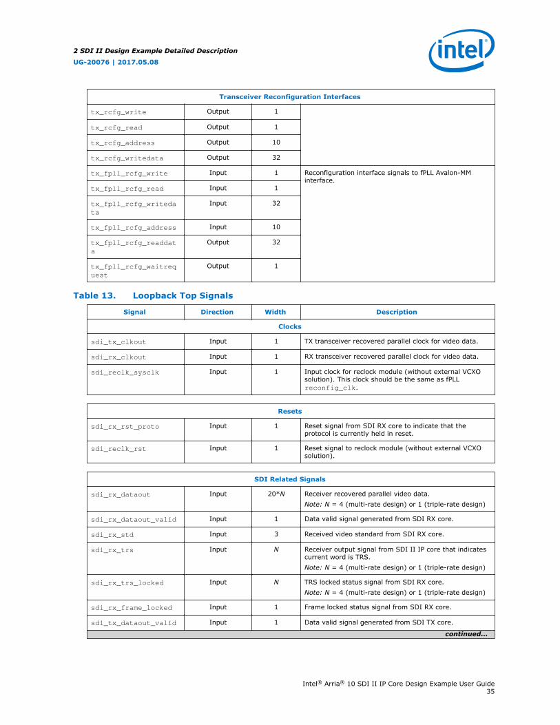
Table 13. Loopback Top Signals
Signal Direction Width Description
Clocks
sdi_tx_clkout Input 1 TX transceiver recovered parallel clock for video data.
sdi_rx_clkout Input 1 RX transceiver recovered parallel clock for video data.
sdi_reclk_sysclk Input 1 Input clock for reclock module (without external VCXOsolution). This clock should be the same as fPLLreconfig_clk.
Resets
sdi_rx_rst_proto Input 1 Reset signal from SDI RX core to indicate that theprotocol is currently held in reset.
sdi_reclk_rst Input 1 Reset signal to reclock module (without external VCXOsolution).
SDI Related Signals
sdi_rx_dataout Input 20*N Receiver recovered parallel video data.Note: N = 4 (multi-rate design) or 1 (triple-rate design)
sdi_rx_dataout_valid Input 1 Data valid signal generated from SDI RX core.
sdi_rx_std Input 3 Received video standard from SDI RX core.
sdi_rx_trs Input N Receiver output signal from SDI II IP core that indicatescurrent word is TRS.Note: N = 4 (multi-rate design) or 1 (triple-rate design)
sdi_rx_trs_locked Input N TRS locked status signal from SDI RX core.Note: N = 4 (multi-rate design) or 1 (triple-rate design)
sdi_rx_frame_locked Input 1 Frame locked status signal from SDI RX core.
sdi_tx_dataout_valid Input 1 Data valid signal generated from SDI TX core.
continued...
2 SDI II Design Example Detailed Description
UG-20076 | 2017.05.08
Intel® Arria® 10 SDI II IP Core Design Example User Guide35

SDI Related Signals
sdi_rx_h Input 1 Horizontal blanking interval timing signal extracted fromSDI RX core.
sdi_rx_format Input 4 Received video transport format.
sdi_rx_clkout_is_ntsc_paln
Input 1 Indication from SDI RX core that the receiver is receivingvideo rate at integer or fractional frame rate.
sdi_tx_datain Output 20*N Parallel video data input to SDI TX core.Note: N = 4 (multi-rate design) or 1 (triple-rate design)
sdi_tx_datain_valid Output 1 Data valid for the transmitter parallel data to SDI TXcore.
sdi_tx_trs Output 1 Transmitter TRS input to indicate that the current word isa TRS to SDI TX core.
sdi_tx_std Output 3 Indicates the desired transmit video standard to SDI TXcore.
Voltage Control Signals for On-board Si516
vcoclk_up Output 1 Voltage up signal to Si516 to increase the voltage.
vcoclk_down Output 1 Voltage down signal to Si516 to decrease the voltage.
fPLL Reconfiguration Signals
pll_locked Input 1 PLL lock status signal.
pll_reconfig_readdata
Input 32 Reconfiguration interface signals to fPLL Avalon-MMinterface.
pll_reconfig_waitrequest
Input 1
pll_reconfig_write Output 1
pll_reconfig_read Output 1
pll_reconfig_writedata
Output 32
pll_reconfig_address Output 10
Table 14. Transceiver Arbiter Signals
Signal Direction Width Description
On-board Oscillator Signals
clk Input 1 Reconfiguration clock. This clock should be sharing thesame clock as reconfiguration management blocks.
reset Input 1 Reset signal. This reset should be sharing the same resetas reconfiguration management blocks.
rx_rcfg_en Input 1 RX reconfiguration enable signal.
tx_rcfg_en Input 1 TX reconfiguration enable signal.
rx_rcfg_ch Input 2 Indicates which channel to be reconfigured on RX.Always assign to 2'b00 for SDI case.
continued...
2 SDI II Design Example Detailed Description
UG-20076 | 2017.05.08
Intel® Arria® 10 SDI II IP Core Design Example User Guide36
Signal Direction Width Description
On-board Oscillator Signals
tx_rcfg_ch Input 2 Indicates which channel to be reconfigured on TX.Always assign to 2'b00 for SDI case.
rx_reconfig_mgmt_write
Input 1 Reconfiguration Avalon-MM interfaces from RXreconfiguration management.
rx_reconfig_mgmt_read
Input 1
rx_reconfig_mgmt_address
Input 10
rx_reconfig_mgmt_writedata
Input 32
rx_reconfig_mgmt_readdata
Output 32
rx_reconfig_mgmt_waitrequest
Output 1
tx_reconfig_mgmt_write
Input 1 Reconfiguration Avalon-MM interfaces from TXreconfiguration management.
tx_reconfig_mgmt_read
Input 1
tx_reconfig_mgmt_address
Input 10
tx_reconfig_mgmt_writedata
Input 32
tx_reconfig_mgmt_readdata
Output 32
tx_reconfig_mgmt_waitrequest
Output 1
reconfig_write Output 1 Reconfiguration Avalon-MM interfaces to transceiver.
reconfig_read Output 1
reconfig_address Output 10
reconfig_writedata Output 32
rx_reconfig_readdata Input 32
rx_reconfig_waitrequest
Input 1
tx_reconfig_readdata Input 1
tx_reconfig_waitrequest
Input 1
rx_cal_busy Input 1 Calibration status signal from RX transceiver.
tx_cal_busy Input 1 Calibration status signal from TX transceiver.
rx_reconfig_cal_busy Output 1 Calibration status signal to RX transceiver PHY resetcontrol.
tx_reconfig_cal_busy Output 1 Calibration status signal from TX transceiver PHY resetcontrol.
2 SDI II Design Example Detailed Description
UG-20076 | 2017.05.08
Intel® Arria® 10 SDI II IP Core Design Example User Guide37

Video Pattern Generator Signals
clk Input 1 Clock signal. This clock must be connected to thetx_vid_clkout input signal on TX/Du top.
rst Input 1 Reset signal. This reset signal should be synchronizedwith the tx_vid_clkout clock signal from the TX/Dutop.
bar_100_75n Input 1 Enable this signal to generate 100% color-bar pattern.Disable to generate 75% color-bar pattern.
enable Input 1 This signal acts as a data valid signal to this module. Thissignal should be connected to the sdi_tx_datavalidsignal from the TX/Du top.
patho Input 1 Enable this signal to generate pathological pattern.
blank Input 1 Enable this signal to generate blank signal.
no_color Input 1 Enable this signal to generate bar with no color.
sgmt_frame Input 1 Enable this signal to generate payload ID for segmentedframe video format when generating 1080i50 or 1080i60video.
tx_std Input 3 Indicates the desired transmit video standard. This inputsignal must match tx_vid_std on the TX/Du top.
tx_format Input 4 Indicates the desired transmit video format.
dl_mapping Input 1 Enable this signal to generate data streams with dual-link mapping.Note: Applicable only for HD dual link or 3G Level B
dual link video standard.
ntsc_paln Input 1 Enable this signal to generate payload ID for fractionalframe rate video format. Disable to generate integerframe rate video format.
dout Output 20*S Data output signal to be connected to the tx_vid_datainput signal on the TX/Du top.
dout_valid Output 1 Data valid output signal to be connected to thetx_vid_datavalid input signal on the TX/Du top.
trs Output 1 TRS output signal to be connected to the tx_vid_trsinput signal on the TX/Du top.
ln Output 11*S Line number output signal to be connected to thesdi_tx_ln input signal on the TX/Du top.
dout_b Output 20*S Data output signal for link B (HD dual link).
dout_valid_b Output 1 Data valid output signal for link B (HD dual link).
trs_b Output 1 TRS output signal for link B (HD dual link).
ln_b Output 11*S Line number output signal to be connected to thesdi_tx_ln_b input signal on the TX/Du top.
vpid_byte1 Input 8*N The payload ID output signal to be connected tosdi_tx_vpid_byte1 input signal on TX/Du top.
vpid_byte2 Input 8*N The payload ID output signal to be connected tosdi_tx_vpid_byte2 input signal on TX/Du top.
vpid_byte3 Input 8*N The payload ID output signal to be connected tosdi_tx_vpid_byte3 input signal on TX/Du top.
continued...
2 SDI II Design Example Detailed Description
UG-20076 | 2017.05.08
Intel® Arria® 10 SDI II IP Core Design Example User Guide38

Video Pattern Generator Signals
vpid_byte4 Input 8*N The payload ID output signal to be connected tosdi_tx_vpid_byte4 input signal on TX/Du top.
vpid_byte1_b Input 8*N The payload ID output signal to be connected tosdi_tx_vpid_byte1_b input signal on TX/Du top.
vpid_byte2_b Input 8*N The payload ID output signal to be connected tosdi_tx_vpid_byte2_b input signal on TX/Du top.
vpid_byte3_b Input 8*N The payload ID output signal to be connected tosdi_tx_vpid_byte3_b input signal on TX/Du top.
vpid_byte4_b Input 8*N The payload ID output signal to be connected tosdi_tx_vpid_byte4_b input signal on TX/Du top.
line_f0 Output 11*N The line number output signal to be inserted with thepayload ID. This signal must connect tosdi_tx_line_f0 input signal on TX/Du top.
line_f1 Output 11*N The line number output signal to be inserted with thepayload ID. This signal must connect tosdi_tx_line_f1 input signal on TX/Du top.
Pattern Generator Control Module Signals
avmm_clk_in_clk Input 1 Clock signal to Avalon-MM interface.
tx_clkout_in_clk Input 1 Clock signal to Parallel I/O (PIO) IP. This clock mustshare the same clock as video pattern generator.
avmm_clk_reset_n Input 1 Reset signal to Avalon-MM interface.
pattgen_rst_reset_in0
Input 1 Input reset signals to a reset synchronizer whichsynchronizes the reset to the tx_clkout_in_clk clockdomain.
pattgen_rst_reset_in1
Input 1
pattgen_rst_reset_out
Input 1 Output reset from the reset synchronizer. This resetsynchronizes to the tx_clkout_in_clk clock domainand connects to the video pattern generator’s inputreset.
pattgen_ctrl_pio_out_port
Output 12 Output control signal from PIO to control the videopattern generator.
2.6 Video Pattern Generator Parameters
Customize the video pattern generator parameters according to your design.
2 SDI II Design Example Detailed Description
UG-20076 | 2017.05.08
Intel® Arria® 10 SDI II IP Core Design Example User Guide39
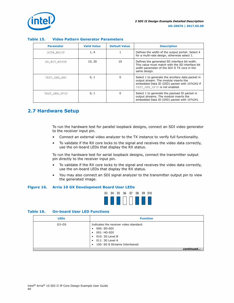
Table 15. Video Pattern Generator Parameters
Parameter Valid Value Default Value Description
OUTW_MULTP 1, 4 1 Defines the width of the output portsh. Select 4for a multi-rate design, otherwise select 1.
SD_BIT_WIDTH 10, 20 10 Defines the generated SD interface bit width.This value must match with the SD interface bitwidth parameter of the SDI II TX core in thesame design.
TEST_GEN_ANC 0, 1 0 Select 1 to generate the ancillary data packet inoutput stream. The module inserts theembedded Data ID (DID) packet with 10’h242 ifTEST_GEN_VPID is not enabled.
TEST_GEN_VPID 0, 1 0 Select 1 to generate the payload ID packet inoutput streams. The module inserts theembedded Data ID (DID) packet with 10’h241.
2.7 Hardware Setup
To run the hardware test for parallel loopback designs, connect an SDI video generatorto the receiver input pin.
• Connect an external video analyzer to the TX instance to verify full functionality.
• To validate if the RX core locks to the signal and receives the video data correctly,use the on-board LEDs that display the RX status.
To run the hardware test for serial loopback designs, connect the transmitter outputpin directly to the receiver input pin.
• To validate if the RX core locks to the signal and receives the video data correctly,use the on-board LEDs that display the RX status.
• You may also connect an SDI signal analyzer to the transmitter output pin to viewthe generated image.
Figure 16. Arria 10 GX Development Board User LEDs
D3 D4 D5 D6 D7 D8 D9 D10
Table 16. On-board User LED Functions
LEDs Function
D3–D5 Indicates the receiver video standard:• 000: SD-SDI• 001: HD-SDI• 010: 3G Level B• 011: 3G Level A• 100: 6G 8 Streams Interleaved
continued...
2 SDI II Design Example Detailed Description
UG-20076 | 2017.05.08
Intel® Arria® 10 SDI II IP Core Design Example User Guide40

LEDs Function
• 101: 6G 4 Streams Interleaved• 110: 12G 16 Streams Interleaved• 111: 12G 8 Streams Interleaved
D6 Shows the slower version of the TX transceiver parallel clock
D7 Shows the slower version of the RX transceiver parallel clock
D8 Illuminates when align_locked asserts
D9 Illuminates when trs_locked asserts
D10 Illuminates when frame_locked asserts
2.8 Simulation Testbench
The simulation testbench checks for the assertion of the trs_locked signal. Thetestbench also detects the number of transceiver reconfiguration triggered after everyvideo standard switching.
Figure 17. Simplex Mode Simulation Testbench Block Diagram
TopRX Top
SDI IIRX
TransceiverPHY Reset
Controller (RX)
TransceiverNative PHY
(RX)
RXReconfigurationManagement (1)
Transceiver Arbiter(1), (2)
SDI RX System
TX Top
SDI IITX
TransceiverPHY Reset
Controller (TX)
TransceiverNative PHY
(TX)
SDI TX System
TXPLL
Alt (2)
Testbench Control
Parallel DataSerial Data
Control/StatusAvalon-MM
Video PatternGenerator
(1) (2)
(1)
(1)
TXPLL
TX ReconfigurationManagement
(2), (3)
(2)
(2)
(2)
(2)
(3)
(1) Block/Connection only required for triple-rate/multi-rate designs.(2) Block/Connection only required for TX PLL switching designs.(3) Block/Connection only required for TX PLL reference clock switching designs.
TX Checker
RX Checker
2 SDI II Design Example Detailed Description
UG-20076 | 2017.05.08
Intel® Arria® 10 SDI II IP Core Design Example User Guide41
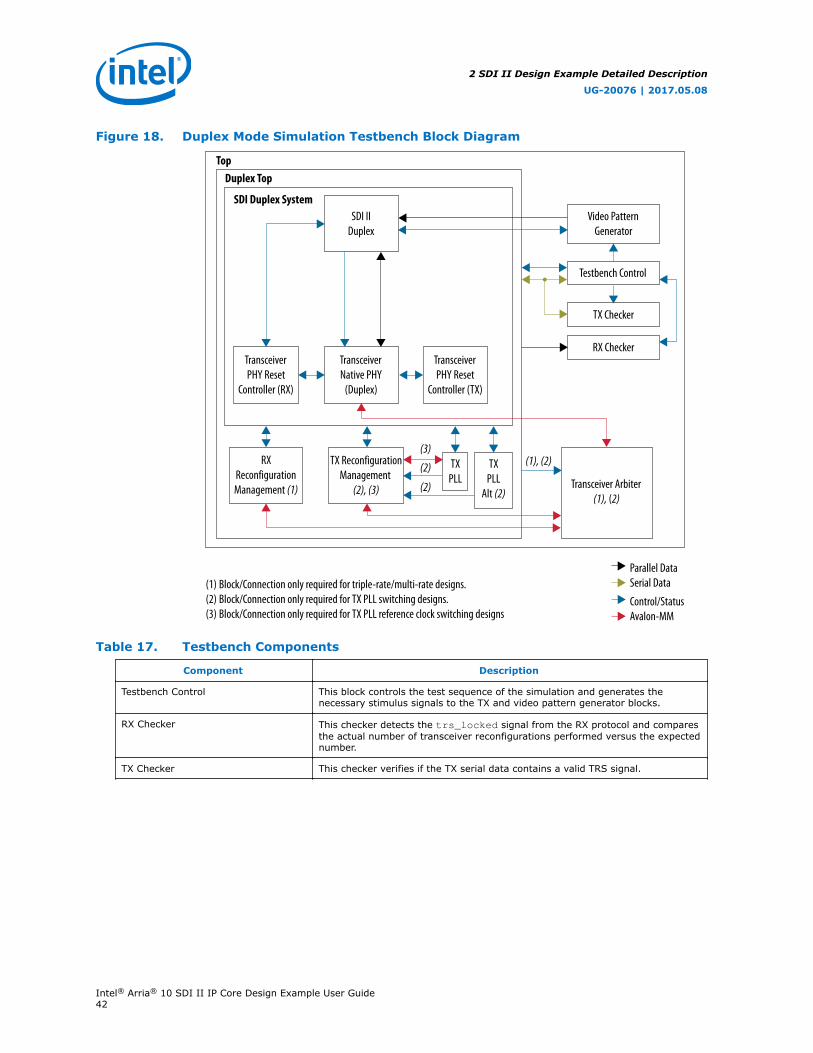
Figure 18. Duplex Mode Simulation Testbench Block Diagram
TopDuplex Top
SDI IIDuplex
TransceiverPHY Reset
Controller (RX)
TransceiverNative PHY
(Duplex)
RXReconfigurationManagement (1) Transceiver Arbiter
(1), (2)
SDI Duplex System
Parallel DataSerial Data
Control/StatusAvalon-MM
TransceiverPHY Reset
Controller (TX)
TXPLL
Alt (2)
TXPLL
TX ReconfigurationManagement
(2), (3)
(2)
(2)
(3)
(1) Block/Connection only required for triple-rate/multi-rate designs.(2) Block/Connection only required for TX PLL switching designs.(3) Block/Connection only required for TX PLL reference clock switching designs
Testbench Control
Video PatternGenerator
TX Checker
RX Checker
(1), (2)
Table 17. Testbench Components
Component Description
Testbench Control This block controls the test sequence of the simulation and generates thenecessary stimulus signals to the TX and video pattern generator blocks.
RX Checker This checker detects the trs_locked signal from the RX protocol and comparesthe actual number of transceiver reconfigurations performed versus the expectednumber.
TX Checker This checker verifies if the TX serial data contains a valid TRS signal.
2 SDI II Design Example Detailed Description
UG-20076 | 2017.05.08
Intel® Arria® 10 SDI II IP Core Design Example User Guide42
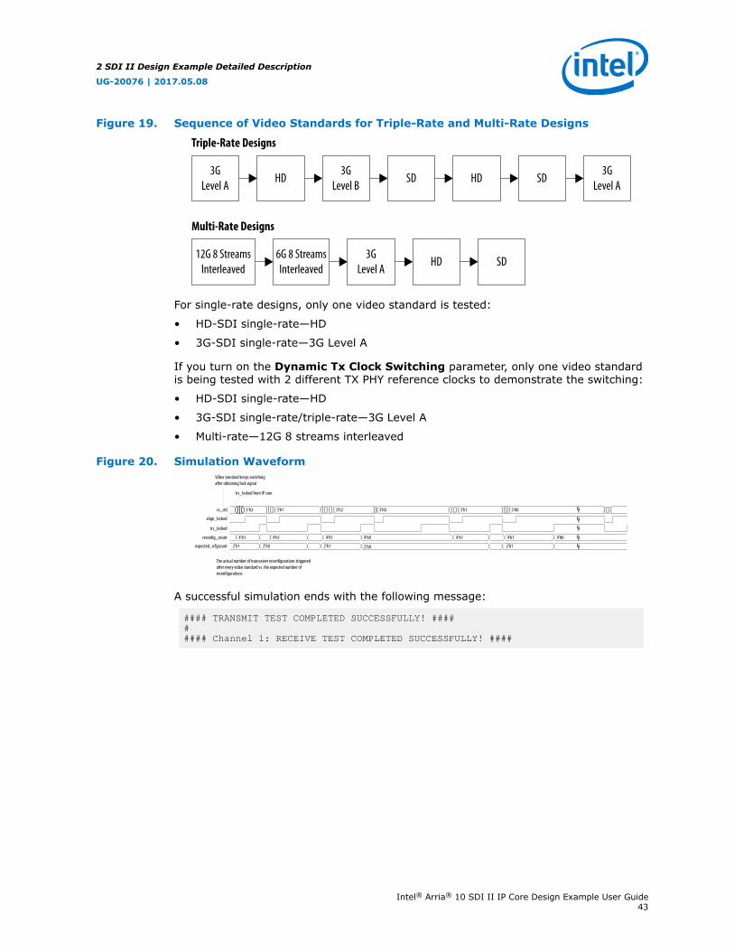
Figure 19. Sequence of Video Standards for Triple-Rate and Multi-Rate Designs
3GLevel A
HD3G
Level BSD HD SD
3GLevel A
Triple-Rate Designs
12G 8 StreamsInterleaved
6G 8 StreamsInterleaved
HD SD
Multi-Rate Designs
3GLevel A
For single-rate designs, only one video standard is tested:
• HD-SDI single-rate—HD
• 3G-SDI single-rate—3G Level A
If you turn on the Dynamic Tx Clock Switching parameter, only one video standardis being tested with 2 different TX PHY reference clocks to demonstrate the switching:
• HD-SDI single-rate—HD
• 3G-SDI single-rate/triple-rate—3G Level A
• Multi-rate—12G 8 streams interleaved
Figure 20. Simulation Waveform
3’h3 3’h1 3’h2 3’h0 3’h1 3’h0
4’h1 4’h14’h14’h14’h1 4’h0 4’h0
2’h1 2’h12’h12’h0 2’h0
rx_std
align_locked
trs_locked
reconfig_count
expected_rcfgcount
Video standard keeps switching after obtaining lock signal
trs_locked from IP core
The actual number of transceiver reconfigurations triggered after every video standard vs. the expected number of reconfigurations
A successful simulation ends with the following message:
#### TRANSMIT TEST COMPLETED SUCCESSFULLY! ##### #### Channel 1: RECEIVE TEST COMPLETED SUCCESSFULLY! ####
2 SDI II Design Example Detailed Description
UG-20076 | 2017.05.08
Intel® Arria® 10 SDI II IP Core Design Example User Guide43
A SDI II IP Core Design Example User Guide ArchivesIf an IP core version is not listed, the user guide for the previous IP core version applies.
IP Core Version User Guide
16.1 SDI II IP Core Design Example User Guide
UG-20076 | 2017.05.08
Intel Corporation. All rights reserved. Intel, the Intel logo, Altera, Arria, Cyclone, Enpirion, MAX, Nios, Quartusand Stratix words and logos are trademarks of Intel Corporation or its subsidiaries in the U.S. and/or othercountries. Intel warrants performance of its FPGA and semiconductor products to current specifications inaccordance with Intel's standard warranty, but reserves the right to make changes to any products and servicesat any time without notice. Intel assumes no responsibility or liability arising out of the application or use of anyinformation, product, or service described herein except as expressly agreed to in writing by Intel. Intelcustomers are advised to obtain the latest version of device specifications before relying on any publishedinformation and before placing orders for products or services.*Other names and brands may be claimed as the property of others.
ISO9001:2008Registered
B Revision History for SDI II IP Core Design ExampleUser Guide
Date Version Changes
May 2017 2017.05.08 • Rebranded as Intel.• Changed the part number.• Updated information about the parallel design examples and added new
information about the serial design example.• Added files designated for Quartus Prime Pro Edition.• Added information about video pattern generator interface signals and
parameters.• Added link to archived version of the Arria 10 SDI II IP Core Design
Example User Guide.
October 2016 2016.10.31 Initial release.
UG-20076 | 2017.05.08
Intel Corporation. All rights reserved. Intel, the Intel logo, Altera, Arria, Cyclone, Enpirion, MAX, Nios, Quartusand Stratix words and logos are trademarks of Intel Corporation or its subsidiaries in the U.S. and/or othercountries. Intel warrants performance of its FPGA and semiconductor products to current specifications inaccordance with Intel's standard warranty, but reserves the right to make changes to any products and servicesat any time without notice. Intel assumes no responsibility or liability arising out of the application or use of anyinformation, product, or service described herein except as expressly agreed to in writing by Intel. Intelcustomers are advised to obtain the latest version of device specifications before relying on any publishedinformation and before placing orders for products or services.*Other names and brands may be claimed as the property of others.
ISO9001:2008Registered