24-channel, 12-bit pwm led driver with internal … · wl0 pulse duration sclk = low-level pulse...
TRANSCRIPT

1FEATURES
APPLICATIONS
DESCRIPTION
¼
SIN
SCLK
XLAT
BLANK
SOUT
VCC
GND
TLC5947
IC1
OUT0 OUT23
¼ ¼
DATA
SCLK
XLAT
BLANK
¼
RIREF
IREF
Controller
3
VCC
¼ ¼
VLED
VLED
¼
VLED
VLED
¼ ¼ ¼
¼
SIN
SCLK
XLAT
BLANK
SOUT
VCC
GND
TLC5947
ICn
OUT0 OUT23
RIREF
IREF
VCC
TLC5947
www.ti.com ................................................................................................................................................. SBVS114A–JULY 2008–REVISED SEPTEMBER 2008
24-Channel, 12-Bit PWM LED Driver withInternal Oscillator
• Noise Reduction:23• 24 Channels, Constant Current Sink Output – 4-channel grouped delay to prevent inrush
current• 30-mA Capability (Constant Current Sink)• Operating Temperature: –40°C to +85°C• 12-Bit (4096 Steps) PWM Grayscale Control
• LED Power-Supply Voltage up to 30 V• VCC = 3.0 V to 5.5 V • Static LED Displays• Constant Current Accuracy: • Message Boards
– Channel-to-Channel = ±2% (typ) • Amusement Illumination– Device-to-Device = ±2% (typ) • TV Backlighting
• CMOS Logic Level I/O• 30-MHz Data Transfer Rate (Standalone)• 15-MHz Data Transfer Rate (Cascaded Devices, The TLC5947 is a 24-channel, constant current sink
SCLK Duty = 50%) LED driver. Each channel is individually adjustablewith 4096 pulse-width modulated (PWM) steps. PWM• Shift Out Data Changes With Falling Edge tocontrol is repeated automatically with theAvoid Data Shift Errors programmed grayscale (GS) data. GS data are
• Auto Display Repeat written via a serial interface port. The current value ofall 24 channels is set by a single external resistor.• 4-MHz Internal Oscillator
• Thermal Shutdown (TSD): The TLC5947 has a thermal shutdown (TSD) functionthat turns off all output drivers during an– Automatic shutdown at over temperatureover-temperature condition. All of the output driversconditionsautomatically restart when the temperature returns to– Restart under normal temperature normal conditions.
1
Please be aware that an important notice concerning availability, standard warranty, and use in critical applications of TexasInstruments semiconductor products and disclaimers thereto appears at the end of this data sheet.
2PowerPAD is a trademark of Texas Instruments, Inc.3All other trademarks are the property of their respective owners.
PRODUCTION DATA information is current as of publication date. Copyright © 2008, Texas Instruments IncorporatedProducts conform to specifications per the terms of the TexasInstruments standard warranty. Production processing does notnecessarily include testing of all parameters.

ABSOLUTE MAXIMUM RATINGS (1) (2)
DISSIPATION RATINGS
TLC5947
SBVS114A–JULY 2008–REVISED SEPTEMBER 2008 ................................................................................................................................................. www.ti.com
This integrated circuit can be damaged by ESD. Texas Instruments recommends that all integrated circuits be handled withappropriate precautions. Failure to observe proper handling and installation procedures can cause damage.
ESD damage can range from subtle performance degradation to complete device failure. Precision integrated circuits may be moresusceptible to damage because very small parametric changes could cause the device not to meet its published specifications.
PACKAGE/ORDERING INFORMATION (1)
PRODUCT PACKAGE-LEAD ORDERING NUMBER TRANSPORT MEDIA, QUANTITYTLC5947DAPR Tape and Reel, 2000
TLC5947 HTSSOP-32 PowerPAD™TLC5947DAP Tube, 46
TLC5947RHBR Tape and Reel, 3000TLC5947 5-mm × 5-mm QFN-32
TLC5947RHB Tape and Reel, 250
(1) For the most current package and ordering information see the Package Option Addendum at the end of this document, or see the TIweb site at www.ti.com.
Over operating free-air temperature range, unless otherwise noted.
PARAMETER TLC5947 UNITVCC Supply voltage: VCC –0.3 to +6.0 VIO Output current (dc) OUT0 to OUT23 38 mAVI Input voltage range SIN, SCLK, XLAT, BLANK –0.3 to VCC + 0.3 V
SOUT –0.3 to VCC + 0.3 VVO Output voltage range
OUT0 to OUT23 –0.3 to +33 VTJ(MAX) Operating junction temperature +150 °CTSTG Storage temperature range –55 to +150 °C
Human body model (HBM) 2 kVESD rating
Charged device model (CDM) 500 V
(1) Stresses above these ratings may cause permanent damage. Exposure to absolute maximum conditions for extended periods maydegrade device reliability. These are stress ratings only, and functional operation of the device at these or any other conditions beyondthose specified is not supported.
(2) All voltage values are with respect to network ground terminal.
OPERATING FACTOR TA < +25°C TA = +70°C TA = +85°CPACKAGE ABOVE TA = +25°C POWER RATING POWER RATING POWER RATING
HTSSOP-32 with 42.54 mW/°C 5318 mW 3403 mW 2765 mWPowerPAD soldered (1)
HTSSOP-32 with 22.56 mW/°C 2820 mW 1805 mW 1466 mWPowerPAD not soldered (2)
QFN-32 (3) 27.86 mW/°C 3482 mW 2228 mW 1811 mW
(1) With PowerPAD soldered onto copper area on printed circuit board (PCB); 2 oz. copper. For more information, see SLMA002 (availablefor download at www.ti.com).
(2) With PowerPAD not soldered onto copper area on PCB.(3) The package thermal impedance is calculated in accordance with JESD51-5.
2 Submit Documentation Feedback Copyright © 2008, Texas Instruments Incorporated
Product Folder Link(s): TLC5947

RECOMMENDED OPERATING CONDITIONS
TLC5947
www.ti.com ................................................................................................................................................. SBVS114A–JULY 2008–REVISED SEPTEMBER 2008
At TA= –40°C to +85°C, unless otherwise noted.
TLC5947PARAMETER TEST CONDITIONS MIN NOM MAX UNIT
DC Characteristics: VCC = 3 V to 5.5 VVCC Supply voltage 3.0 5.5 VVO Voltage applied to output OUT0 to OUT23 30 VVIH High-level input voltage 0.7 × VCC VCC VVIL Low-level input voltage GND 0.3 × VCC VIOH High-level output current SOUT –3 mAIOL Low-level output current SOUT 3 mAIOLC Constant output sink current OUT0 to OUT23 2 30 mA
Operating free-air temperatureTA –40 +85 °CrangeTJ Operating junction temperature –40 +125 °CAC Characteristics: VCC = 3 V to 5.5 V
SCLK, Standalone operation 30 MHzfSCLK Data shift clock frequency
SCLK, Duty 50%, cascade operation 15 MHzTWH0 SCLK = High-level pulse width 12 nsTWL0 Pulse duration SCLK = Low-level pulse width 10 nsTWH1 XLAT, BLANK High-level pulse width 30 nsTSU0 SIN–SCLK↑ 5 nsTSU1 Setup time XLAT↑–SCLK↑ 100 nsTSU2 XLAT↑–BLANK↓ 30 nsTH0 SIN–SCLK↑ 3 ns
Hold timeTH1 XLAT↑–SCLK↑ 10 ns
Copyright © 2008, Texas Instruments Incorporated Submit Documentation Feedback 3
Product Folder Link(s): TLC5947

ELECTRICAL CHARACTERISTICS
D (%) =IOUTn
- 1(I + I + ... + I )OUT0 OUT1 OUT22 + IOUT23
24
´ 100
.
D (%) =Ideal Output Current
- (Ideal Output Current)(I + I + ... I + I )OUT0 OUT1 OUT22 OUT23
24´ 100
I = 41 ´OUT(IDEAL)
1.20
RIREF
100
(I at V = 3.0 V)OUTn CC
(I at V = 5.5 V) (I at V = 3.0 V)OUTn CC OUTn CC-
5.5 V 3 V-
D (%/V) = ´
100
3 V 1 V-
´
(I at V = 1 V)OUTn OUTn
(I at V = 3 V) (I at V = 1 V)-OUTn OUTn OUTn OUTnD (%/V) =
TLC5947
SBVS114A–JULY 2008–REVISED SEPTEMBER 2008 ................................................................................................................................................. www.ti.com
At VCC = 3.0 V to 5.5 V and TA = –40°C to +85°C. Typical values at VCC = 3.3 V and TA = +25°C, unless otherwise noted.TLC5947
PARAMETER TEST CONDITIONS MIN TYP MAX UNIT
VOH High-level output voltage IOH = –3 mA at SOUT VCC – 0.4 VCC V
VOL Low-level output voltage IOL = 3 mA at SOUT 0.4 V
IIN Input current VIN = VCC or GND at SIN, XLAT, and BLANK –1 1 µA
SIN/SCLK/XLAT = low, BLANK = high, VOUTn = 1 V,ICC1 0.5 3 mARIREF = 24 kΩ
SIN/SCLK/XLAT = low, BLANK = high, VOUTn = 1 V,ICC2 1 6 mARIREF = 3.3 kΩSupply current (VCC)
SIN/SCLK/XLAT = low, BLANK = low, VOUTn = 1 V,ICC3 15 45 mARIREF = 3.3 kΩ, GSn = FFFh
SIN/SCLK/XLAT = low, BLANK = low, VOUTn = 1 V,ICC4 30 90 mARIREF = 1.6 kΩ, GSn = FFFh
All OUTn = ON, VOUTn = 1 V, VOUTfix = 1 V,IOLC Constant output current 27.7 30.75 33.8 mARIREF = 1.6 kΩ
BLANK = high, VOUTn = 30 V, RIREF = 1.6 kΩ,IOLK Output leakage current 0.1 µAAt OUT0 to OUT23
Constant current error All OUTn = ON, VOUTn = 1 V, VOUTfix = 1 V,ΔIOLC ±2 ±4 %(channel-to-channel) (1) RIREF = 1.6 kΩ, At OUT0 to OUT23
Constant current error All OUTn = ON, VOUTn = 1 V, VOUTfix = 1 V,ΔIOLC1 ±2 ±7 %(device-to-device) (2) RIREF = 1.6 kΩ
All OUTn = ON, VOUTn = 1 V, VOUTfix = 1 V,ΔIOLC2 Line regulation (3) ±1 ±3 %/VRIREF = 1.6 kΩ, At OUT0 to OUT23
All OUTn = ON, VOUTn = 1 V to 3 V, VOUTfix = 1 V,ΔIOLC3 Load regulation (4) ±2 ±6 %/VRIREF = 1.6 kΩ, At OUT0 to OUT23
TDOWN Thermal shutdown threshold Junction temperature (5) +150 +162 +175 °C
THYS Thermal error hysteresis Junction temperature (5) +5 +10 +20 °C
VIREF Reference voltage output RIREF = 1.6 kΩ 1.16 1.20 1.24 V
(1) The deviation of each output from the average of OUT0–OUT23 constant current. Deviation is calculated by the formula:
(2) The deviation of the OUT0–OUT23 constant current average from the ideal constant current value.Deviation is calculated by the following formula:
Ideal current is calculated by the formula:
(3) Line regulation is calculated by this equation:
(4) Load regulation is calculated by the equation:
(5) Not tested. Specified by design.
4 Submit Documentation Feedback Copyright © 2008, Texas Instruments Incorporated
Product Folder Link(s): TLC5947

SWITCHING CHARACTERISTICS
FUNCTIONAL BLOCK DIAGRAM
SCLK
IREF
XLAT
GND
G yscalra e (12 Bits 24 Ch´ annels) Data
Shift Register
12 Bits PWM Timing Control
OUT0
Thermal
Detection
VCC
OU 23T
SOUT
4 MHz
Internal
Oscillator
OUT1 OU 22T
288
LSB MSB
0 287
VCC
SIN
Grayscale (12 Bits 24 C´ hannels) Data
Data Latch
LSB
0
288
MSB
287
BL NKA
24-Channel, C nstant Curreo nt Driver
24
D Q
CK
¼
TLC5947
www.ti.com ................................................................................................................................................. SBVS114A–JULY 2008–REVISED SEPTEMBER 2008
At VCC = 3.0 V to 5.5 V, TA = –40°C to +85°C, CL = 15 pF, RL = 150 Ω, RIREF = 1.6 kΩ, and VLED = 5.5 V. Typical values atVCC = 3.3 V and TA = +25°C, unless otherwise noted.
TLC5947PARAMETER TEST CONDITIONS MIN TYP MAX UNIT
tR0 SOUT 10 15 nsRise time
tR1 OUTn 15 40 nstF0 SOUT 10 15 ns
Fall timetF1 OUTn 100 300 ns
Internal oscillatorfOSC 2.4 4 5.6 MHzfrequencytD0 SCLK↓ to SOUT 15 25 nstD1 BLANK↑ to OUT0 sink current off 20 40 nstD2 Propagation delay time OUT0 current on to OUT1/5/9/13/17/21 current on 15 24 33 nstD3 OUT0 current on to OUT2/6/10/14/18/22 current on 30 48 66 nstD4 OUT0 current on to OUT3/7/11/15/19/23 current on 45 72 99 ns
Copyright © 2008, Texas Instruments Incorporated Submit Documentation Feedback 5
Product Folder Link(s): TLC5947

DEVICE INFORMATION
Thermal Pad
(Bottom Side)
OU
T0
OU
T1
OU
T2
OU
T3
OU
T4
OU
T5
OU
T6
OU
T7
OU
T2
3
OU
T2
2
OU
T2
1
OU
T2
0
OU
T1
9
OU
T1
8
OU
T1
7
OU
T1
6
1 2 3 4 5 6 7 8
24
23
22
21
20
19
18
17
SIN 32 OUT8
SCLK OUT9
BLANK OUT10
GND OUT11
VCC OUT12
IREF OUT13
XLAT OUT14
SOUT OUT15
9
1031
1130
1229
1328
1427
1526
1625
GND
BLANK
SCLK
SIN
OUT0
OUT1
OUT2
OUT3
OUT4
OUT5
OUT6
OUT7
1
2
3
4
5
6
7
8
9
10
11
12
13
14
OUT8
OUT9
15
16
OUT10
OUT11
VCC
IREF
XLAT
SOUT
OUT23
OUT22
OUT21
OUT20
OUT19
OUT18
OUT17
OUT16
OUT15
OUT14
28
27
26
25
24
23
22
21
20
19
18
17
OUT13
OUT12
32
31
30
29
Thermal Pad
(Bottom Side)
TLC5947
SBVS114A–JULY 2008–REVISED SEPTEMBER 2008 ................................................................................................................................................. www.ti.com
HTSSOP-32 5-mm × 5-mm QFN-32(1)DAP PACKAGE RHB PACKAGE
(TOP VIEW) (TOP VIEW)
(1) This device is product preview.
NOTE: Thermal pad is not connected to GND internally. The thermal pad must be connected to GND via the PCBpattern.
6 Submit Documentation Feedback Copyright © 2008, Texas Instruments Incorporated
Product Folder Link(s): TLC5947

TLC5947
www.ti.com ................................................................................................................................................. SBVS114A–JULY 2008–REVISED SEPTEMBER 2008
TERMINAL FUNCTIONSTERMINAL
NAME DAP RHB I/O DESCRIPTIONSIN 4 32 I Serial input for grayscale data
Serial data shift clock. Schmitt buffer input. Data present on the SIN pin are shifted into the shiftregister with the rising edge of the SCLK pin. Data are shifted to the MSB side by 1-bitSCLK 3 31 I synchronizing of the rising edge of SCLK. The MSB data appears on SOUT at the falling edge ofSCLK. A rising edge on the SCLK input is allowed 100 ns after an XLAT rising edge.The data in the grayscale shift register are moved to the grayscale data latch with a low-to-hightransition on this pin. When the XLAT rising edge is input, all constant current outputs are forcedXLAT 30 26 I off until the next grayscale display period. The grayscale counter is not reset to zero with a risingedge of XLAT.Blank (all constant current outputs off). When BLANK is high, all constant current outputs (OUT0through OUT23) are forced off, the grayscale PWM timing controller initializes, and the grayscaleBLANK 2 30 I counter resets to '0'. When BLANK is low, all constant current outputs are controlled by thegrayscale PWM timing controller.This pin sets the constant current value. OUT0 through OUT23 constant sink current is set to theIREF 31 27 I/O desired value by connecting an external resistor between IREF and GND.Serial data output. This output is connected to the shift register placed after the MSB of thegrayscale shift register. Therefore, the MSB data of the grayscale shift register appears at theSOUT 29 25 O falling edge of SCLK. This function reduces the data shifting errors caused by small timingmargins between SIN and SCLK.Constant current output. Multiple outputs can be tied together to increase the constant currentOUT0 5 1 O capability. Different voltages can be applied to each output.
OUT1 6 2 O Constant current outputOUT2 7 3 O Constant current outputOUT3 8 4 O Constant current outputOUT4 9 5 O Constant current outputOUT5 10 6 O Constant current outputOUT6 11 7 O Constant current outputOUT7 12 8 O Constant current outputOUT8 13 9 O Constant current outputOUT9 14 10 O Constant current outputOUT10 15 11 O Constant current outputOUT11 16 12 O Constant current outputOUT12 17 13 O Constant current outputOUT13 18 14 O Constant current outputOUT14 19 15 O Constant current outputOUT15 20 16 O Constant current outputOUT16 21 17 O Constant current outputOUT17 22 18 O Constant current outputOUT18 23 19 O Constant current outputOUT19 24 20 O Constant current outputOUT20 25 21 O Constant current outputOUT21 26 22 O Constant current outputOUT22 27 23 O Constant current outputOUT23 28 24 O Constant current outputVCC 32 28 — Power-supply voltageGND 1 29 — Power ground
Copyright © 2008, Texas Instruments Incorporated Submit Documentation Feedback 7
Product Folder Link(s): TLC5947

PARAMETER MEASUREMENT INFORMATION
PIN EQUIVALENT INPUT AND OUTPUT SCHEMATIC DIAGRAMSVCC
INPUT
GND
VCC
SOUT
GND
OUTn
GND
TEST CIRCUITS
VCC
VCC
GND
IREF OUTn
RIREF
RL
CL
VLED V
CC
VCC
GND
SOUT
CL
¼¼
VCC
RIREF
VOUTFIX
VOUTn
OUT0VCC
OUTn
OUT23GND
IREF
TLC5947
SBVS114A–JULY 2008–REVISED SEPTEMBER 2008 ................................................................................................................................................. www.ti.com
Figure 1. SIN, SCLK, XLAT, BLANK Figure 2. SOUT
Figure 3. OUT0 Through OUT23
Figure 4. Rise Time and Fall Time Test Circuit for OUTn Figure 5. Rise Time and Fall Time Test Circuit for SOUT
Figure 6. Constant Current Test Circuit for OUTn
8 Submit Documentation Feedback Copyright © 2008, Texas Instruments Incorporated
Product Folder Link(s): TLC5947
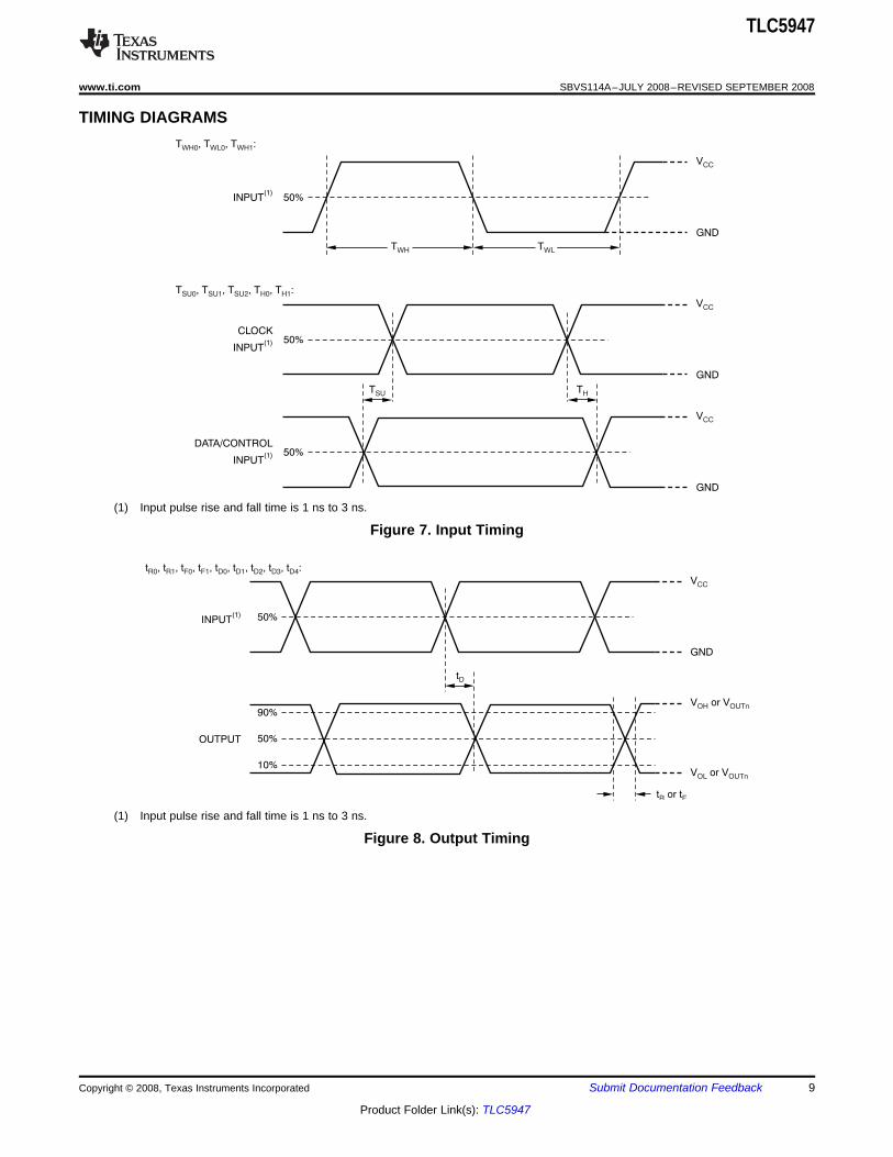
TIMING DIAGRAMST , T, T :WH0 WH1WL0
INPUT(1)
CLOCK
INPUT(1)
DATA/CONTROL
INPUT(1)
T , T , T , T , T :SU0 SU1 SU2 H0 H1
TSU TH
VCC
VCC
GND
VCC
GND
GND
50%
50%
50%
TWH TWL
t , t , t , t , t , t , t , t , t :R0 R1 F0 F1 D0 D1 D2 D3 D4
INPUT(1) 50%
50%
90%
10%
OUTPUT
tD
t or tR F
V or VOL OUTn
V or VOH OUTn
GND
VCC
TLC5947
www.ti.com ................................................................................................................................................. SBVS114A–JULY 2008–REVISED SEPTEMBER 2008
(1) Input pulse rise and fall time is 1 ns to 3 ns.
Figure 7. Input Timing
(1) Input pulse rise and fall time is 1 ns to 3 ns.
Figure 8. Output Timing
Copyright © 2008, Texas Instruments Incorporated Submit Documentation Feedback 9
Product Folder Link(s): TLC5947

t /tR0 F0
GS237A
GS02B
tD1
1 2 3 4 5 6 7285 286 287 288
tF1
tD4
tD3
tD2
TWH1
SIN
OUT0/4/8/
12/16/20(1)
OUT1/5/9/
13/17/21(1)
OUT2/6/10/
14/18/22(1)
OUT3/7/11/
15/19/23(1)
ON
OFF
XLAT
Grayscale
Latch Data
(Internal)
BLANK
SOUT
ON
OFF
ON
OFF
ON
OFF
TWH0
TWH1
TSU0 fSCLK
tD0
tR1
GS2311B
GS2310B
GS00A
GS239B
GS238B
GS237B
GS00B
GS01B
GS03B
GS2311A
GS239A
GS238A
GS03A
GS02A
GS01A
GS00A
GS2311B
GS2310A
TH0
Previous Grayscale Data Latest Grayscale Data
SCLK
1 2 3 4 5
TH1
TSU2
Oscillator
Clock
(Internal)
TWL0
0 0 0 0 1 2 3 4 5 0 0 0 0 0 1 2fOSC
GS2311C
GS2310C
GS239C
GS238C
GS237C
GS236C
GS235C
GS2310B
GS239B
GS238B
GS237B
GS236B
GS235B
Counter
Value
TSU1
40934094
4095 1 2 3 44096
¼ ¼ ¼ ¼
TLC5947
SBVS114A–JULY 2008–REVISED SEPTEMBER 2008 ................................................................................................................................................. www.ti.com
(1) GS data = FFFh.
Figure 9. Grayscale Data Write and OUTn Operation Timing
10 Submit Documentation Feedback Copyright © 2008, Texas Instruments Incorporated
Product Folder Link(s): TLC5947

TYPICAL CHARACTERISTICS
100000
10000
10000 5 10 15 20 30
Output Current (mA)
Refe
rence R
esis
tor
()
W
25
9840
4920
32802460
1640
1968
24600
6000
5000
4000
3000
2000
1000
0
-40 -20 0 20 40 60 80
Free-Air Temperature ( C)°
Pow
er
Dis
sip
ation R
ate
(m
W)
TLC5947RHB
TLC5947DAP
PowerPAD Soldered
TLC5947DAP
PowerPAD Not Soldered
100
35
30
25
20
15
10
5
00 0.5 1.0 1.5 2.0 2.5 3.0
Output Voltage (V)
Outp
ut C
urr
ent (m
A)
T = +25 C°A I = 30 mAO
I = 25 mAO
I = 20 mAO
I = 15 mAO
I = 10 mAO
I = 5 mAOI = 2 mAO
35
34
33
32
31
30
29
28
27
26
250 0.5 1.0 1.5 2.0 2.5 3.0
Output Voltage (V)
Outp
ut C
urr
ent (m
A)
I = 30 mAO
T = 40- °CA
T = +25 C°A
T = +85 C°A
4
3
2
1
0
1
2
3
4
-
-
-
-
-40 -20 0 20 40 60 80 100
Ambient Temperature ( C)°
DI
(%)
OLC
I = 30 mAO
V = 5 VCC
V = 3.3 VCC
4
3
2
1
0
1
2
3
4
-
-
-
-
0 5 10 15 20 25 30
Output Current (mA)
DI
(%)
OLC
T = +25 C°A
V = 5 VCC
V = 3.3 VCC
TLC5947
www.ti.com ................................................................................................................................................. SBVS114A–JULY 2008–REVISED SEPTEMBER 2008
At VCC = 3.3 V and TA = +25°C, unless otherwise noted.
REFERENCE RESISTOR POWER DISSIPATION RATEvs OUTPUT CURRENT vs FREE-AIR TEMPERATURE
Figure 10. Figure 11.
OUTPUT CURRENT vs OUTPUT CURRENT vsOUTPUT VOLTAGE OUTPUT VOLTAGE
Figure 12. Figure 13.
ΔIOLC vs AMBIENT TEMPERATURE ΔIOLC vs OUTPUT CURRENT
Figure 14. Figure 15.
Copyright © 2008, Texas Instruments Incorporated Submit Documentation Feedback 11
Product Folder Link(s): TLC5947

Time (100 ns/div)
CH3-OUT23
(GSData = 003h)
C 2-OUT0
(GSData = 002h)
H
CH1-OUT0
(GSData = 001h)CH1 (2 V/div)
CH2 (2 V/div)
CH3 (2 V/div)
I = 30 mA
T = +25 C
R = 150
C = 15 pF
VLED = 5.5 V
°
W
OLCMax
A
L
L
5.0
4.5
4.0
3.5
3.0
2.5
2.0
1.5
1.0
0.5
0-40 -20 0 20 35 55 70
Ambient Temperature ( C)°
Inte
rnal O
scill
ato
r F
requency (
MH
z)
V = +3.3 VCC
85
V = +5 VCC
TLC5947
SBVS114A–JULY 2008–REVISED SEPTEMBER 2008 ................................................................................................................................................. www.ti.com
TYPICAL CHARACTERISTICS (continued)At VCC = 3.3 V and TA = +25°C, unless otherwise noted.
INTERNAL OSCILLATOR FREQUENCY CONSTANT CURRENT OUTPUTvs AMBIENT TEMPERATURE VOLTAGE WAVEFORM
Figure 16. Figure 17.
12 Submit Documentation Feedback Copyright © 2008, Texas Instruments Incorporated
Product Folder Link(s): TLC5947

DETAILED DESCRIPTION
SETTING FOR THE CONSTANT SINK CURRENT VALUE
R ( ) = 41WIREF ´
V (V)IREF
I (mA)OLC (1)
GRAYSCALE (GS) CONTROL FUNCTION
TLC5947
www.ti.com ................................................................................................................................................. SBVS114A–JULY 2008–REVISED SEPTEMBER 2008
The constant current value for all channels is set by an external resistor (RIREF) placed between IREF and GND.The resistor (RIREF) value is calculated by Equation 1.
Where:VIREF = the internal reference voltage on the IREF pin (typically 1.20 V).
IOLC must be set in the range of 2 mA to 30 mA. The constant sink current characteristic for the external resistorvalue is shown in Figure 10. Table 1 describes the constant current output versus external resistor value.
Table 1. Constant-Current Output versus External Resistor ValueIOLC (mA, Typical) RIREF (Ω)
30 164025 196820 246015 328010 49205 98402 24600
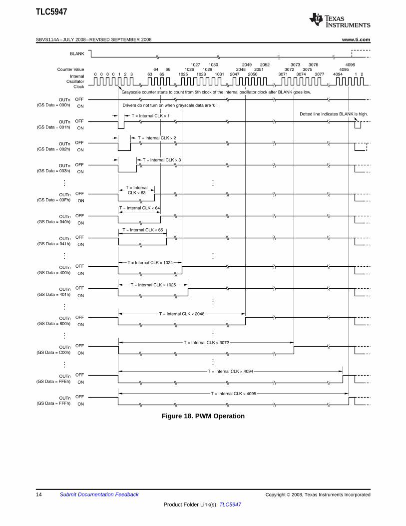
Each constant current sink output OUT0–OUT23 (OUTn) turns on (starts to sink constant current) at the fifthrising edge of the grayscale internal oscillator clock after the BLANK signal transitions from high to low if thegrayscale data latched into the grayscale data latch are not zero. After turn-on, the number of rising edges of theinternal oscillator is counted by the 12-bit grayscale counter. Each OUTn output is turned off once itscorresponding grayscale data values equal the grayscale counter or the counter reaches 4096d (FFFh). ThePWM control operation is repeated as long as BLANK is low. OUTn is not turned on when BLANK is high. Thetiming is shown in Figure 18. All outputs are turned off at the XLAT rising edge. After that, each output iscontrolled again from the first clock of the internal oscillator for the next display period, based on the latestgrayscale data.
When the IC is powered on, the data in the grayscale data shift register and latch are not set to default values.Therefore, grayscale data must be written to the GS latch before turning on the constant current output. BLANKshould be at a high level when powered on to keep the outputs off until valid grayscale data are written to thelatch. This avoids the LED being randomly illuminated immediately after power-up. If having the outputs turn onat power-up is not a problem for the application, then BLANK does not need to be held high. The grayscalefunctions can be controlled directly by grayscale data writing, even though BLANK is connected to GND.
Copyright © 2008, Texas Instruments Incorporated Submit Documentation Feedback 13
Product Folder Link(s): TLC5947
T = Internal CLK 65´
Internal
Oscillator
Clock
BLANK
OUTn
(GS Data = 000h) ON
OFF
OUTn
(GS Data = 001h) ON
OFF
OUTn
(GS Data = 002h) ON
OFF
ON
OFFOUTn
(GS Data = 003h)
OUTn
(GS Data = 03Fh) ON
OFF
OFFOUTn
(GS Data = 040h) ON
ON
OFFOUTn
(GS Data = 041h)
OUTn
(GS Data = 400h) ON
OFF
ON
OFFOUTn
(GS Data = 401h)
ON
OFF
ON
OFF
OUTn
(GS Data = FFFh) ON
OFF
0 0 0 0 1 2 3
T = Internal CLK 64´
63 6564 66
1025 1028 10311026 1029
1027 1030
3071 3074 30773072 3075
3073
4094 1 24095
40963076
2047 20502048 2051
2049 2052
OUTn
(GS Data = FFEh)
OUTn
(GS Data = 800h)
OUTn
(GS Data = C00h) ON
OFF
Counter Value
¼¼
¼
¼¼
¼¼
¼
¼¼
T = Internal
CLK 63´
T = Internal CLK 4095´
T = Internal CLK 4094´
T = Internal CLK 1024´
T = Internal CLK 1025´
T = Internal CLK 2048´
T = Internal CLK 3072´
T = Internal CLK 1´
T = Internal CLK 2´
Drivers do not turn on when grayscale data are ‘0’.
T = Internal CLK 3´
Grayscale counter starts to count from 5th BLANK goes low.clock of the internal oscillator clock after
Dotted line indicates BLANK is high.
TLC5947
SBVS114A–JULY 2008–REVISED SEPTEMBER 2008 ................................................................................................................................................. www.ti.com
Figure 18. PWM Operation
14 Submit Documentation Feedback Copyright © 2008, Texas Instruments Incorporated
Product Folder Link(s): TLC5947

REGISTER CONFIGURATION
¼ ¼ ¼
Grayscale Shift Register (12 Bits 24 Channels)´Data
Grayscale Data Latch (12 Bits 24 Channels)´ 288 Bits
To PWM Timing Control Block
¼ ¼ ¼SOUT
GS Data for OUT23 GS Data for OUT22 GS Data for OUT1¼ GS Data for OUT0
MSB287 276 275 12 11
LSB0
GS Data for
Bit 0 of OUT1
GS Data for
Bit 11 of
OUT0
GS Data for
Bit 0 of OUT0
GS Data for
Bit 0 of
OUT23
GS Data for
Bit 11 of
OUT22
GS Data for
Bit 11 of
OUT23
SIN
SCLK
¼ ¼ ¼
GS Data for OUT23 GS Data for OUT22 GS Data for OUT1¼ GS Data for OUT0
MSB287 276 275 12 11
LSB0
GS Data for
Bit 0 of OUT1
GS Data for
Bit 11 of
OUT0
GS Data for
Bit 0 of OUT0
GS Data for
Bit 0 of
OUT23
GS Data for
Bit 11 of
OUT22
GS Data for
Bit 11 of
OUT23XLAT
TLC5947
www.ti.com ................................................................................................................................................. SBVS114A–JULY 2008–REVISED SEPTEMBER 2008
The TLC5947 has a grayscale (GS) data shift register and data latch. Both the GS data shift register and latchare 288 bits long and are used to set the PWM timing for the constant current driver. Table 2 shows the on dutycycle for each GS data. Figure 19 shows the shift register and data latch configuration. The data at the SIN pinare shifted to the LSB of the shift register at the rising edge of the SCLK pin; SOUT data are shifted out on thefalling edge of SCLK. The timing diagram for data writing is shown in Figure 20. The driver on duty is controlledby the data in the GS data latch.
Figure 19. Grayscale Data Shift Register and Latch Configuration
Table 2. GS Data versus On DutyGS DATA GS DATA GS DATA DUTY OF DRIVER TURN-ON(Binary) (Decimal) (Hex) TIME (%)
0000 0000 0000 0 000 0.000000 0000 0001 1 001 0.020000 0000 0010 2 002 0.050000 0000 0011 3 003 0.07
— — — —0111 1111 1111 2047 7FF 49.981000 0000 0000 2048 800 50.001000 0000 0001 2049 801 50.02
— — — —1111 1111 1101 4093 FFD 99.931111 1111 1110 4094 FFE 99.951111 1111 1111 4095 FFF 99.98
Copyright © 2008, Texas Instruments Incorporated Submit Documentation Feedback 15
Product Folder Link(s): TLC5947

On Duty (%) =GSn
4096´ 100
(2)
GS235B
GS00A
1 2 3 4 5
GS00A
GS03A
GS02B
1 2 3 4 5 6 7285 286 287 288
SIN
ON
OFF
XLAT
SOUT
ON
ON
OFF
ON
OFF
GS2311B
GS2310B
GS239B
GS238B
GS237B
GS00B
GS01B
GS03B
GS2311A
GS239A
GS238A
GS237A
GS02A
GS01A
GS00A
GS2311B
GS2310A
Latest Grayscale Latch Data
SCLK
GS2311C
GS2310C
GS239C
GS238C
GS237C
GS236C
GS2310B
GS239B
GS238B
GS237B
GS236B
GS02B
GS2311B
GS2310B
GS239B
GS238B
GS00B
GS01B
GS03B
GS2311C
GS2310C
GS239C
GS238C
GS237C
GS236C
4094
4093 1 2 3 44095
4096
ON
ON
ON
ON
OFF
OFF
OFF
OFF
ON
ON
ON
ON
OFF
ON
GS01A
GS03B
GS00A
GS2311B
GS2310B
GS239B
GS01B
GS02B
GS04B
GS00B
GS2311C
GS2310C
GS239C
GS238C
GS237C
GS2311A
GS01A
GS2310A
GS239A
GS238A
GS237A
GS2311B
GS230A
GS02A
GS2310B
GS239B
GS238B
GS237B
GS236B
GS235B
GS2310A
GS00A
GS239A
GS238A
GS237A
GS236A
GS2310B
GS2311B
GS01A
GS239B
GS238B
GS237B
GS236B
GS235B
GS234B
Shift Register
Bit 0 Data (Internal)
Shift Register
Bit 1 Data (Internal)
Shift Register
Bit 286 Data (Internal)
Shift Register
Bit 287 Data (Internal)
Previous Grayscale Latch DataGrayscale Latch Data
(Internal)
Oscillator Clock
(Internal)
OUT2/6/10/14/18/22(1)
OUT3/7/11/15/19/23(1)
OUT0/4/8/12/16/20(1)
OUT1/5/9/13/17/21(1)
¼ ¼ ¼ ¼
¼ ¼
4094
4093 1 2 3 4 5 6 7 84095
4096
¼ ¼
TLC5947
SBVS114A–JULY 2008–REVISED SEPTEMBER 2008 ................................................................................................................................................. www.ti.com
GS data are transferred from the shift register to the latch by the rising edge of XLAT. When powered up, thedata in the grayscale shift register and data latch are not set to default values. Therefore, grayscale data must bewritten to the GS latch before turning on the constant current output. BLANK should be at a high level whenpowered on to avoid falsely turning on the constant current outputs due to random values in the latch atpower-up. All of the constant current outputs are forced off when BLANK is high. However, if the random valuesturning on at power-up is not a concern in the application, BLANK can be at any level. GS can be controlledcorrectly with the grayscale data writing functions, even if BLANK is connected to GND. Equation 2 determineseach output on duty.
where:GSn = the programmed grayscale value for OUTn (GSn = 0 to 4095)
(1) GS data = FFFh.
Figure 20. Grayscale Data Write Operation
16 Submit Documentation Feedback Copyright © 2008, Texas Instruments Incorporated
Product Folder Link(s): TLC5947

AUTO DISPLAY REPEAT FUNCTION
First
Display Period
Internal Oscillator Clock
BLANK
OUTn
(GS Data = 001h)
1 2 3 20472048
2049 40944095
0 1 2 3 20472048
2049 40944095
0 1 2 3 0 2140964095
40942100000
Nth Display Period
Display period is turned on again by
the auto display repeat function.
OFF
ON
OUTn
(GS Data = 800h)
OFF
OUTn
(GS Data = FFFh)
OFF
ON
ON
GS Counter Value
Second
Display Period
0 0 0 0
Four Internal Clock Intervals After BLANK Goes Low Four Internal Clock Intervals After BLANK Goes Low
First Display Period
(4096 Internal Clock)
Second Display Period
(4096 Internal Clock)
Grayscale counter starts to count from the fifth clock
of the internal oscillator clock after BLANK goes low.
¼ ¼ ¼ ¼ ¼
THERMAL SHUTDOWN (TSD)
IC Junction Temperature (T )J
OUTn
(GS Data = FFFh)
Internal Oscillator Clock
1 2 3 4095
4096
1 2 4095
4096
1 2 4095
4096
1 2 4095
4096
1 2 4095
4096
1 2 4095
4096
1 2
ON
T < T - TJ (TEF) (HYS) T T³J (TEF)
OFF
BLANK
T < T - TJ (TEF) (HYS) T T³J (TEF)
OFF
ON
OFF
High
Low
TLC5947
www.ti.com ................................................................................................................................................. SBVS114A–JULY 2008–REVISED SEPTEMBER 2008
This function can repeat the total display period without any timing control signal, as shown in Figure 21.
Figure 21. Auto Display Repeat Operation
The thermal shutdown (TSD) function turns off all constant current outputs immediately when the IC junctiontemperature exceeds the high temperature threshold (T(TEF) = +162° C, typ). The outputs will remain disabled aslong as the over-temperature condition exists. The outputs are turned on again at the first clock after the ICjunction temperature falls below the temperature of T(TEF) – T(HYS). Figure 22 shows the TSD operation.
Figure 22. TSD Operation
Copyright © 2008, Texas Instruments Incorporated Submit Documentation Feedback 17
Product Folder Link(s): TLC5947

NOISE REDUCTION
POWER DISSIPATION CALCULATION
P = (V I ) + (V I )´D CC CC OUT OLC´ ´ ´N dPWM (3)
TLC5947
SBVS114A–JULY 2008–REVISED SEPTEMBER 2008 ................................................................................................................................................. www.ti.com
Large surge currents may flow through the IC and the board on which the device is mounted if all 24 LEDchannels turn on simultaneously at the start of each grayscale cycle. These large current surges could introducedetrimental noise and electromagnetic interference (EMI) into other circuits. The TLC5947 turns on the LEDchannels in a series delay, to provide a current soft-start feature. The output current sinks are grouped into fourgroups of six channels each. The first group is OUT0, 4, 8, 12, 16, 20; the second group is OUT1, 5, 9, 13, 17,21; the third group is OUT2, 6, 10, 14, 18, 22; and the fourth group is OUT3, 7, 11, 15, 19, 23. Each group turnson sequentially with a small delay between groups; see Figure 9. Both turn-on and turn-off are delayed.
The device power dissipation must be below the power dissipation rate of the device package (illustrated inFigure 11) to ensure correct operation. Equation 3 calculates the power dissipation of the device:
Where:• VCC = device supply voltage• ICC = device supply current• VOUT = OUTn voltage when driving LED current• IOLC = LED current adjusted by RIREF resistor• N = number of OUTn driving LED at the same time• dPWM = duty ratio defined by GS value
18 Submit Documentation Feedback Copyright © 2008, Texas Instruments Incorporated
Product Folder Link(s): TLC5947

PACKAGE OPTION ADDENDUM
www.ti.com 23-Feb-2012
Addendum-Page 1
PACKAGING INFORMATION
Orderable Device Status (1) Package Type PackageDrawing
Pins Package Qty Eco Plan (2) Lead/Ball Finish
MSL Peak Temp (3) Samples
(Requires Login)
TLC5947DAP ACTIVE HTSSOP DAP 32 46 Green (RoHS& no Sb/Br)
CU NIPDAU Level-3-260C-168 HR
TLC5947DAPG4 ACTIVE HTSSOP DAP 32 46 Green (RoHS& no Sb/Br)
CU NIPDAU Level-3-260C-168 HR
TLC5947DAPR ACTIVE HTSSOP DAP 32 2000 Green (RoHS& no Sb/Br)
CU NIPDAU Level-3-260C-168 HR
TLC5947DAPRG4 ACTIVE HTSSOP DAP 32 2000 Green (RoHS& no Sb/Br)
CU NIPDAU Level-3-260C-168 HR
TLC5947RHBR ACTIVE QFN RHB 32 3000 Green (RoHS& no Sb/Br)
CU NIPDAU Level-2-260C-1 YEAR
TLC5947RHBRG4 ACTIVE QFN RHB 32 3000 Green (RoHS& no Sb/Br)
CU NIPDAU Level-2-260C-1 YEAR
TLC5947RHBT ACTIVE QFN RHB 32 250 Green (RoHS& no Sb/Br)
CU NIPDAU Level-2-260C-1 YEAR
TLC5947RHBTG4 ACTIVE QFN RHB 32 250 Green (RoHS& no Sb/Br)
CU NIPDAU Level-2-260C-1 YEAR
(1) The marketing status values are defined as follows:ACTIVE: Product device recommended for new designs.LIFEBUY: TI has announced that the device will be discontinued, and a lifetime-buy period is in effect.NRND: Not recommended for new designs. Device is in production to support existing customers, but TI does not recommend using this part in a new design.PREVIEW: Device has been announced but is not in production. Samples may or may not be available.OBSOLETE: TI has discontinued the production of the device.
(2) Eco Plan - The planned eco-friendly classification: Pb-Free (RoHS), Pb-Free (RoHS Exempt), or Green (RoHS & no Sb/Br) - please check http://www.ti.com/productcontent for the latest availabilityinformation and additional product content details.TBD: The Pb-Free/Green conversion plan has not been defined.Pb-Free (RoHS): TI's terms "Lead-Free" or "Pb-Free" mean semiconductor products that are compatible with the current RoHS requirements for all 6 substances, including the requirement thatlead not exceed 0.1% by weight in homogeneous materials. Where designed to be soldered at high temperatures, TI Pb-Free products are suitable for use in specified lead-free processes.Pb-Free (RoHS Exempt): This component has a RoHS exemption for either 1) lead-based flip-chip solder bumps used between the die and package, or 2) lead-based die adhesive used betweenthe die and leadframe. The component is otherwise considered Pb-Free (RoHS compatible) as defined above.Green (RoHS & no Sb/Br): TI defines "Green" to mean Pb-Free (RoHS compatible), and free of Bromine (Br) and Antimony (Sb) based flame retardants (Br or Sb do not exceed 0.1% by weightin homogeneous material)
(3) MSL, Peak Temp. -- The Moisture Sensitivity Level rating according to the JEDEC industry standard classifications, and peak solder temperature.

PACKAGE OPTION ADDENDUM
www.ti.com 23-Feb-2012
Addendum-Page 2
Important Information and Disclaimer:The information provided on this page represents TI's knowledge and belief as of the date that it is provided. TI bases its knowledge and belief on informationprovided by third parties, and makes no representation or warranty as to the accuracy of such information. Efforts are underway to better integrate information from third parties. TI has taken andcontinues to take reasonable steps to provide representative and accurate information but may not have conducted destructive testing or chemical analysis on incoming materials and chemicals.TI and TI suppliers consider certain information to be proprietary, and thus CAS numbers and other limited information may not be available for release.
In no event shall TI's liability arising out of such information exceed the total purchase price of the TI part(s) at issue in this document sold by TI to Customer on an annual basis.

TAPE AND REEL INFORMATION
*All dimensions are nominal
Device PackageType
PackageDrawing
Pins SPQ ReelDiameter
(mm)
ReelWidth
W1 (mm)
A0(mm)
B0(mm)
K0(mm)
P1(mm)
W(mm)
Pin1Quadrant
TLC5947DAPR HTSSOP DAP 32 2000 330.0 24.4 8.6 11.5 1.6 12.0 24.0 Q1
TLC5947RHBR QFN RHB 32 3000 330.0 12.4 5.3 5.3 1.5 8.0 12.0 Q2
TLC5947RHBT QFN RHB 32 250 180.0 12.4 5.3 5.3 1.5 8.0 12.0 Q2
PACKAGE MATERIALS INFORMATION
www.ti.com 14-Jul-2012
Pack Materials-Page 1

*All dimensions are nominal
Device Package Type Package Drawing Pins SPQ Length (mm) Width (mm) Height (mm)
TLC5947DAPR HTSSOP DAP 32 2000 367.0 367.0 45.0
TLC5947RHBR QFN RHB 32 3000 367.0 367.0 35.0
TLC5947RHBT QFN RHB 32 250 210.0 185.0 35.0
PACKAGE MATERIALS INFORMATION
www.ti.com 14-Jul-2012
Pack Materials-Page 2


IMPORTANT NOTICE
Texas Instruments Incorporated and its subsidiaries (TI) reserve the right to make corrections, enhancements, improvements and otherchanges to its semiconductor products and services per JESD46, latest issue, and to discontinue any product or service per JESD48, latestissue. Buyers should obtain the latest relevant information before placing orders and should verify that such information is current andcomplete. All semiconductor products (also referred to herein as “components”) are sold subject to TI’s terms and conditions of salesupplied at the time of order acknowledgment.
TI warrants performance of its components to the specifications applicable at the time of sale, in accordance with the warranty in TI’s termsand conditions of sale of semiconductor products. Testing and other quality control techniques are used to the extent TI deems necessaryto support this warranty. Except where mandated by applicable law, testing of all parameters of each component is not necessarilyperformed.
TI assumes no liability for applications assistance or the design of Buyers’ products. Buyers are responsible for their products andapplications using TI components. To minimize the risks associated with Buyers’ products and applications, Buyers should provideadequate design and operating safeguards.
TI does not warrant or represent that any license, either express or implied, is granted under any patent right, copyright, mask work right, orother intellectual property right relating to any combination, machine, or process in which TI components or services are used. Informationpublished by TI regarding third-party products or services does not constitute a license to use such products or services or a warranty orendorsement thereof. Use of such information may require a license from a third party under the patents or other intellectual property of thethird party, or a license from TI under the patents or other intellectual property of TI.
Reproduction of significant portions of TI information in TI data books or data sheets is permissible only if reproduction is without alterationand is accompanied by all associated warranties, conditions, limitations, and notices. TI is not responsible or liable for such altereddocumentation. Information of third parties may be subject to additional restrictions.
Resale of TI components or services with statements different from or beyond the parameters stated by TI for that component or servicevoids all express and any implied warranties for the associated TI component or service and is an unfair and deceptive business practice.TI is not responsible or liable for any such statements.
Buyer acknowledges and agrees that it is solely responsible for compliance with all legal, regulatory and safety-related requirementsconcerning its products, and any use of TI components in its applications, notwithstanding any applications-related information or supportthat may be provided by TI. Buyer represents and agrees that it has all the necessary expertise to create and implement safeguards whichanticipate dangerous consequences of failures, monitor failures and their consequences, lessen the likelihood of failures that might causeharm and take appropriate remedial actions. Buyer will fully indemnify TI and its representatives against any damages arising out of the useof any TI components in safety-critical applications.
In some cases, TI components may be promoted specifically to facilitate safety-related applications. With such components, TI’s goal is tohelp enable customers to design and create their own end-product solutions that meet applicable functional safety standards andrequirements. Nonetheless, such components are subject to these terms.
No TI components are authorized for use in FDA Class III (or similar life-critical medical equipment) unless authorized officers of the partieshave executed a special agreement specifically governing such use.
Only those TI components which TI has specifically designated as military grade or “enhanced plastic” are designed and intended for use inmilitary/aerospace applications or environments. Buyer acknowledges and agrees that any military or aerospace use of TI componentswhich have not been so designated is solely at the Buyer's risk, and that Buyer is solely responsible for compliance with all legal andregulatory requirements in connection with such use.
TI has specifically designated certain components which meet ISO/TS16949 requirements, mainly for automotive use. Components whichhave not been so designated are neither designed nor intended for automotive use; and TI will not be responsible for any failure of suchcomponents to meet such requirements.
Products Applications
Audio www.ti.com/audio Automotive and Transportation www.ti.com/automotive
Amplifiers amplifier.ti.com Communications and Telecom www.ti.com/communications
Data Converters dataconverter.ti.com Computers and Peripherals www.ti.com/computers
DLP® Products www.dlp.com Consumer Electronics www.ti.com/consumer-apps
DSP dsp.ti.com Energy and Lighting www.ti.com/energy
Clocks and Timers www.ti.com/clocks Industrial www.ti.com/industrial
Interface interface.ti.com Medical www.ti.com/medical
Logic logic.ti.com Security www.ti.com/security
Power Mgmt power.ti.com Space, Avionics and Defense www.ti.com/space-avionics-defense
Microcontrollers microcontroller.ti.com Video and Imaging www.ti.com/video
RFID www.ti-rfid.com
OMAP Applications Processors www.ti.com/omap TI E2E Community e2e.ti.com
Wireless Connectivity www.ti.com/wirelessconnectivity
Mailing Address: Texas Instruments, Post Office Box 655303, Dallas, Texas 75265Copyright © 2012, Texas Instruments Incorporated