2300 mhz to 2900 mhz balanced mixer, lo buffer and … · 2300 mhz to 2900 mhz balanced mixer, lo...
TRANSCRIPT
2300 MHz to 2900 MHz Balanced Mixer,LO Buffer and RF Balun
ADL5363
Rev. 0 Information furnished by Analog Devices is believed to be accurate and reliable. However, no responsibility is assumed by Analog Devices for its use, nor for any infringements of patents or other rights of third parties that may result from its use. Specifications subject to change without notice. No license is granted by implication or otherwise under any patent or patent rights of Analog Devices. Trademarks and registered trademarks are the property of their respective owners.
One Technology Way, P.O. Box 9106, Norwood, MA 02062-9106, U.S.A.Tel: 781.329.4700 www.analog.com Fax: 781.461.3113 ©2011 Analog Devices, Inc. All rights reserved.
FEATURES RF frequency range of 2300 MHz to 2900 MHz IF frequency range of dc to 450 MHz Power conversion loss: 7.7 dB SSB noise figure of 7.6 dB Input IP3 of 31 dBm Typical LO drive of 0 dBm Single-ended, 50 Ω RF and LO input ports High isolation SPDT LO input switch Single-supply operation: 3.3 V to 5 V Exposed pad, 5 mm × 5 mm 20-lead LFCSP 1500 V HBM/1250 V FICDM ESD performance
APPLICATIONS Cellular base station receivers Transmit observation receivers Radio link downconverters
GENERAL DESCRIPTION The ADL5363 uses a highly linear, doubly balanced passive mixer core along with integrated RF and local oscillator (LO) balancing circuitry to allow for single-ended operation. The ADL5363 incorporates an RF balun to provide optimal performance over a 2300 MHz to 2900 MHz input frequency range. The balanced passive mixer arrangement provides good LO-to-RF leakage, typically better than −30 dBm, and excellent intermodulation performance. The balanced mixer core also provides extremely high input linearity, allowing the device to be used in demanding cellular applications where in-band blocking signals might otherwise result in the degradation of dynamic performance.
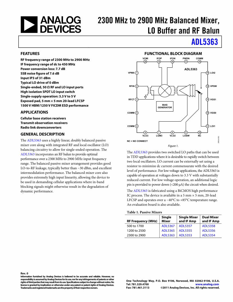
FUNCTIONAL BLOCK DIAGRAM
2
3
1
20 19 18 17 16
6 7 8 9 10
4
5
14
13
15
12
BIASGENERATOR
VPMX
RFIN
RFCT
COMM
COMM
LOI2
VPSW
VGS1
VGS0
LOI1
VCMI IFOP IFON PWDN COMM
VLO3 LGM3 VLO2 LOSW NC
ADL5363
NC = NO CONNECT
11
0991
4-00
1
Figure 1.
The ADL5363 provides two switched LO paths that can be used in TDD applications where it is desirable to rapidly switch between two local oscillators. LO current can be externally set using a resistor to minimize dc current commensurate with the desired level of performance. For low voltage applications, the ADL5363 is capable of operation at voltages down to 3.3 V with substantially reduced current. For low voltage operation, an additional logic pin is provided to power down (<200 μA) the circuit when desired.
The ADL5363 is fabricated using a BiCMOS high performance IC process. The device is available in a 5 mm × 5 mm, 20-lead LFCSP and operates over a −40°C to +85°C temperature range. An evaluation board is also available.
Table 1. Passive Mixers
RF Frequency (MHz) Single Mixer
Single Mixerand IF Amp
Dual Mixer and IF Amp
500 to 1700 ADL5367 ADL5357 ADL5358 1200 to 2500 ADL5365 ADL5355 ADL5356 2300 to 2900 ADL5363 ADL5353 ADL5354
ADL5363
Rev. 0 | Page 2 of 24
TABLE OF CONTENTS Features .............................................................................................. 1
Applications....................................................................................... 1
General Description ......................................................................... 1
Functional Block Diagram .............................................................. 1
Revision History ............................................................................... 2
Specifications..................................................................................... 3
5 V Performance........................................................................... 4
3.3 V Performance........................................................................ 4
Absolute Maximum Ratings............................................................ 5
ESD Caution.................................................................................. 5
Pin Configuration and Function Descriptions............................. 6
Typical Performance Characteristics ............................................. 7
5 V Performance........................................................................... 7
3.3 V Performance...................................................................... 14
Upconversion.............................................................................. 15
Spurious Performance ............................................................... 16
Circuit Description......................................................................... 17
RF Subsystem.............................................................................. 17
LO Subsystem ............................................................................. 18
Applications Information .............................................................. 19
Basic Connections...................................................................... 19
IF Port .......................................................................................... 19
Bias Resistor Selection ............................................................... 19
Mixer VGS Control DAC .......................................................... 19
Evaluation Board ............................................................................ 20
Outline Dimensions ....................................................................... 23
Ordering Guide .......................................................................... 23
REVISION HISTORY 7/11—Revision 0: Initial Version
ADL5363
Rev. 0 | Page 3 of 24
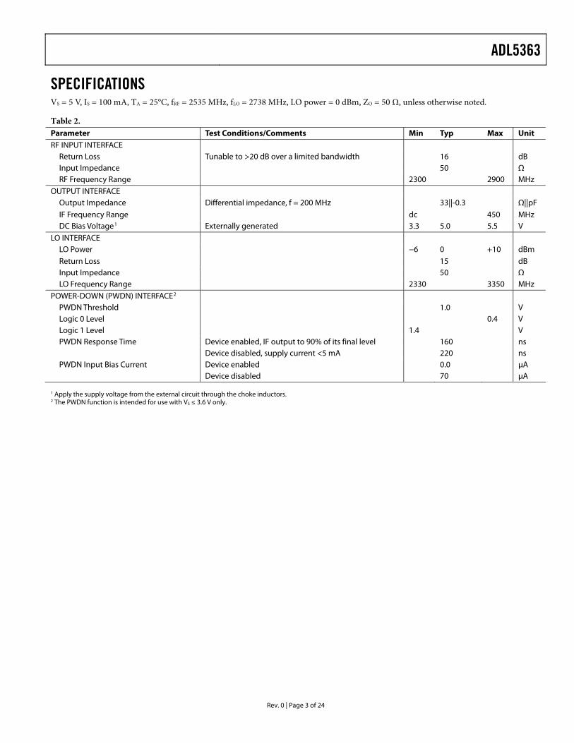
SPECIFICATIONS VS = 5 V, IS = 100 mA, TA = 25°C, fRF = 2535 MHz, fLO = 2738 MHz, LO power = 0 dBm, ZO = 50 Ω, unless otherwise noted.
Table 2. Parameter Test Conditions/Comments Min Typ Max Unit RF INPUT INTERFACE
Return Loss Tunable to >20 dB over a limited bandwidth 16 dB Input Impedance 50 Ω RF Frequency Range 2300 2900 MHz
OUTPUT INTERFACE Output Impedance Differential impedance, f = 200 MHz 33||-0.3 Ω||pF IF Frequency Range dc 450 MHz DC Bias Voltage1 Externally generated 3.3 5.0 5.5 V
LO INTERFACE LO Power −6 0 +10 dBm Return Loss 15 dB Input Impedance 50 Ω LO Frequency Range 2330 3350 MHz
POWER-DOWN (PWDN) INTERFACE2 PWDN Threshold 1.0 V Logic 0 Level 0.4 V Logic 1 Level 1.4 V PWDN Response Time Device enabled, IF output to 90% of its final level 160 ns Device disabled, supply current <5 mA 220 ns PWDN Input Bias Current Device enabled 0.0 μA
Device disabled 70 μA 1 Apply the supply voltage from the external circuit through the choke inductors. 2 The PWDN function is intended for use with VS ≤ 3.6 V only.
ADL5363
Rev. 0 | Page 4 of 24
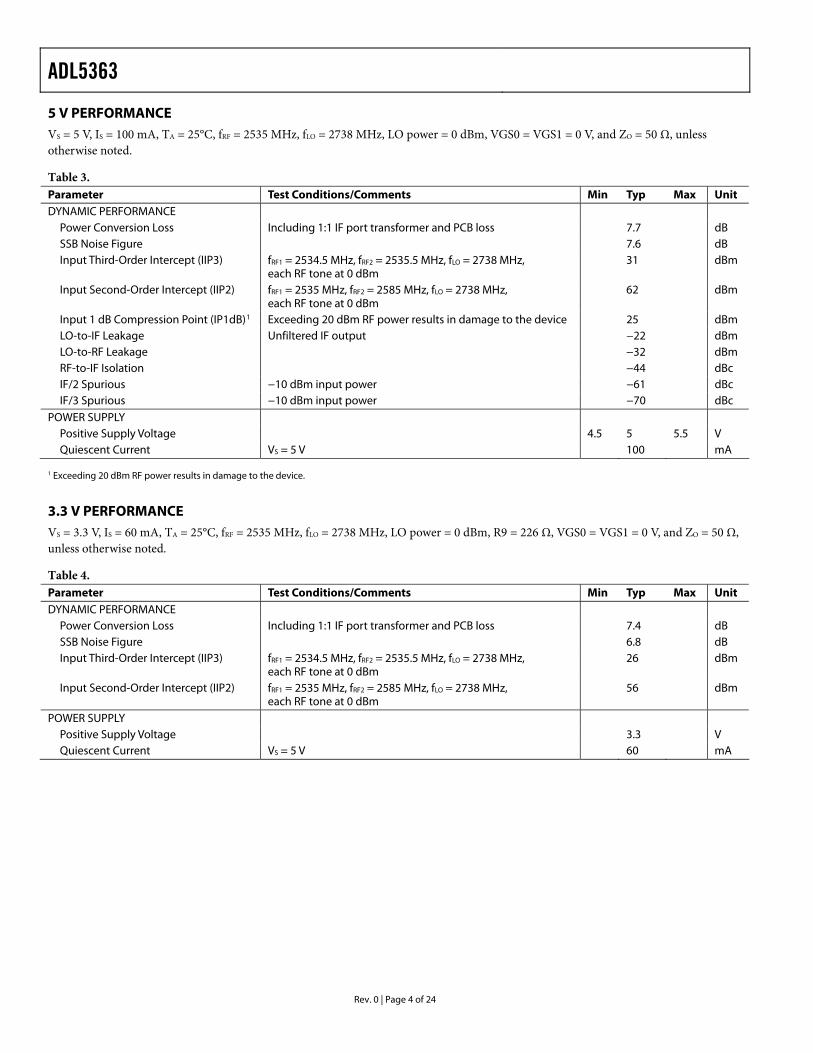
5 V PERFORMANCE VS = 5 V, IS = 100 mA, TA = 25°C, fRF = 2535 MHz, fLO = 2738 MHz, LO power = 0 dBm, VGS0 = VGS1 = 0 V, and ZO = 50 Ω, unless otherwise noted.
Table 3. Parameter Test Conditions/Comments Min Typ Max Unit DYNAMIC PERFORMANCE
Power Conversion Loss Including 1:1 IF port transformer and PCB loss 7.7 dB SSB Noise Figure 7.6 dB Input Third-Order Intercept (IIP3) fRF1 = 2534.5 MHz, fRF2 = 2535.5 MHz, fLO = 2738 MHz,
each RF tone at 0 dBm 31 dBm
Input Second-Order Intercept (IIP2) fRF1 = 2535 MHz, fRF2 = 2585 MHz, fLO = 2738 MHz, each RF tone at 0 dBm
62 dBm
Input 1 dB Compression Point (IP1dB)1 Exceeding 20 dBm RF power results in damage to the device 25 dBm LO-to-IF Leakage Unfiltered IF output −22 dBm LO-to-RF Leakage −32 dBm RF-to-IF Isolation −44 dBc IF/2 Spurious −10 dBm input power −61 dBc IF/3 Spurious −10 dBm input power −70 dBc
POWER SUPPLY Positive Supply Voltage 4.5 5 5.5 V Quiescent Current VS = 5 V 100 mA
1 Exceeding 20 dBm RF power results in damage to the device.
3.3 V PERFORMANCE VS = 3.3 V, IS = 60 mA, TA = 25°C, fRF = 2535 MHz, fLO = 2738 MHz, LO power = 0 dBm, R9 = 226 Ω, VGS0 = VGS1 = 0 V, and ZO = 50 Ω, unless otherwise noted.
Table 4. Parameter Test Conditions/Comments Min Typ Max Unit DYNAMIC PERFORMANCE
Power Conversion Loss Including 1:1 IF port transformer and PCB loss 7.4 dB SSB Noise Figure 6.8 dB Input Third-Order Intercept (IIP3) fRF1 = 2534.5 MHz, fRF2 = 2535.5 MHz, fLO = 2738 MHz,
each RF tone at 0 dBm 26 dBm
Input Second-Order Intercept (IIP2) fRF1 = 2535 MHz, fRF2 = 2585 MHz, fLO = 2738 MHz, each RF tone at 0 dBm
56 dBm
POWER SUPPLY Positive Supply Voltage 3.3 V Quiescent Current VS = 5 V 60 mA
ADL5363
Rev. 0 | Page 5 of 24
ABSOLUTE MAXIMUM RATINGS Table 5. Parameter Rating Supply Voltage, VS 5.5 V RF Input Level 20 dBm LO Input Level 13 dBm IFOP, IFON Bias Voltage 6.0 V VGS0, VGS1, LOSW, PWDN 5.5 V Internal Power Dissipation 0.5 W Thermal Resistance, θJA 25°C/W Temperature
Maximum Junction Temperature 150°C Operating Temperature Range −40°C to +85°C Storage Temperature Range −65°C to +150°C Lead Temperature (Soldering, 60 sec) 260°C
Stresses above those listed under Absolute Maximum Ratings may cause permanent damage to the device. This is a stress rating only; functional operation of the device at these or any other conditions above those indicated in the operational section of this specification is not implied. Exposure to absolute maximum rating conditions for extended periods may affect device reliability.
ESD CAUTION
ADL5363
Rev. 0 | Page 6 of 24
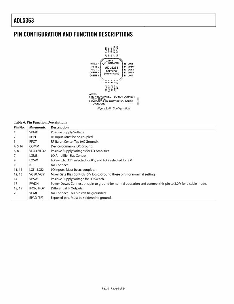
PIN CONFIGURATION AND FUNCTION DESCRIPTIONS
PIN 1INDICATOR
NOTES1.
2
NC = NO CONNECT. DO NOT CONNECTTO THIS PIN.
. EXPOSED PAD. MUST BE SOLDEREDTO GROUND.
1VPMX2RFIN3RFCT4COMM5COMM
13 VGS114 VPSW15 LOI2
12 VGS011 LOI1
6VL
O3
7LG
M3
8VL
O2
10N
C9
LOSW
18IF
ON
19IF
OP
20VC
MI
17PW
DN
16C
OM
M
TOP VIEW(Not to Scale)
ADL5363
0991
4-00
2
Figure 2. Pin Configuration
Table 6. Pin Function Descriptions Pin No. Mnemonic Description 1 VPMX Positive Supply Voltage. 2 RFIN RF Input. Must be ac-coupled. 3 RFCT RF Balun Center Tap (AC Ground). 4, 5,16 COMM Device Common (DC Ground). 6, 8 VLO3, VLO2 Positive Supply Voltages for LO Amplifier. 7 LGM3 LO Amplifier Bias Control. 9 LOSW LO Switch. LOI1 selected for 0 V, and LOI2 selected for 3 V. 10 NC No Connect. 11, 15 LOI1, LOI2 LO Inputs. Must be ac-coupled. 12, 13 VGS0, VGS1 Mixer Gate Bias Controls. 3 V logic. Ground these pins for nominal setting. 14 VPSW Positive Supply Voltage for LO Switch. 17 PWDN Power Down. Connect this pin to ground for normal operation and connect this pin to 3.0 V for disable mode. 18, 19 IFON, IFOP Differential IF Outputs. 20 VCMI No Connect. This pin can be grounded. EPAD (EP) Exposed pad. Must be soldered to ground.
ADL5363
Rev. 0 | Page 7 of 24
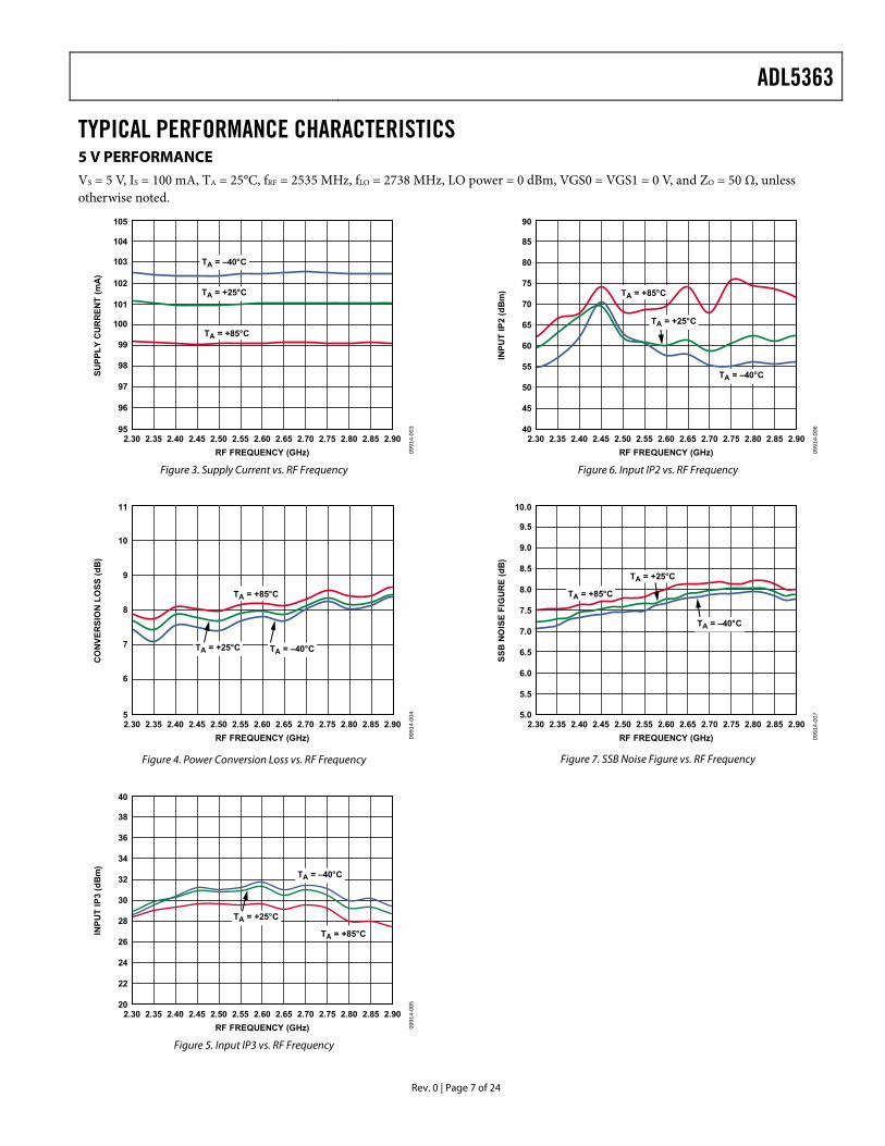
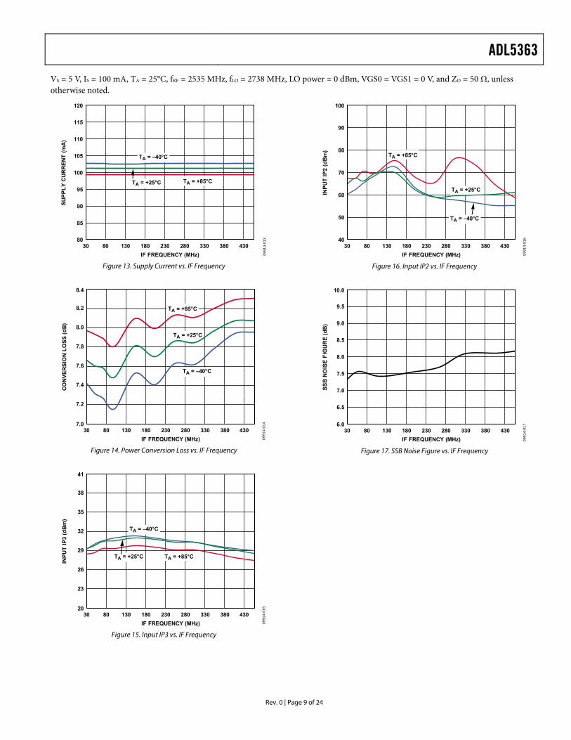
TYPICAL PERFORMANCE CHARACTERISTICS 5 V PERFORMANCE VS = 5 V, IS = 100 mA, TA = 25°C, fRF = 2535 MHz, fLO = 2738 MHz, LO power = 0 dBm, VGS0 = VGS1 = 0 V, and ZO = 50 Ω, unless otherwise noted.
105
104
103
102
101
100
99
98
97
96
952.30 2.35 2.40 2.45 2.50 2.55 2.60 2.65 2.902.852.802.752.70
SUPP
LY C
UR
REN
T (m
A)
RF FREQUENCY (GHz) 0991
4-00
3
TA = –40°C
TA = +25°C
TA = +85°C
Figure 3. Supply Current vs. RF Frequency
11
10
9
8
6
7
52.30 2.35 2.40 2.45 2.50 2.55 2.60 2.65 2.902.852.802.752.70
CO
NVE
RSI
ON
LO
SS (d
B)
RF FREQUENCY (GHz) 0991
4-00
4
TA = +85°C
TA = +25°C TA = –40°C
Figure 4. Power Conversion Loss vs. RF Frequency
40
38
36
34
30
28
26
24
22
32
202.30 2.35 2.40 2.45 2.50 2.55 2.60 2.65 2.902.852.802.752.70
INPU
T IP
3 (d
Bm
)
RF FREQUENCY (GHz) 0991
4-00
5
TA = +85°C
TA = –40°C
TA = +25°C
Figure 5. Input IP3 vs. RF Frequency
90
85
80
75
65
60
55
50
45
70
402.30 2.35 2.40 2.45 2.50 2.55 2.60 2.65 2.902.852.802.752.70
INPU
T IP
2 (d
Bm
)
RF FREQUENCY (GHz) 0991
4-00
6
TA = +85°C
TA = –40°C
TA = +25°C
Figure 6. Input IP2 vs. RF Frequency
10.0
9.5
8.5
8.0
7.5
7.0
6.5
9.0
5.0
6.0
5.5
2.30 2.35 2.40 2.45 2.50 2.55 2.60 2.65 2.902.852.802.752.70
SSB
NO
ISE
FIG
UR
E (d
B)
RF FREQUENCY (GHz) 0991
4-00
7
TA = +85°C
TA = –40°C
TA = +25°C
Figure 7. SSB Noise Figure vs. RF Frequency
ADL5363
Rev. 0 | Page 8 of 24
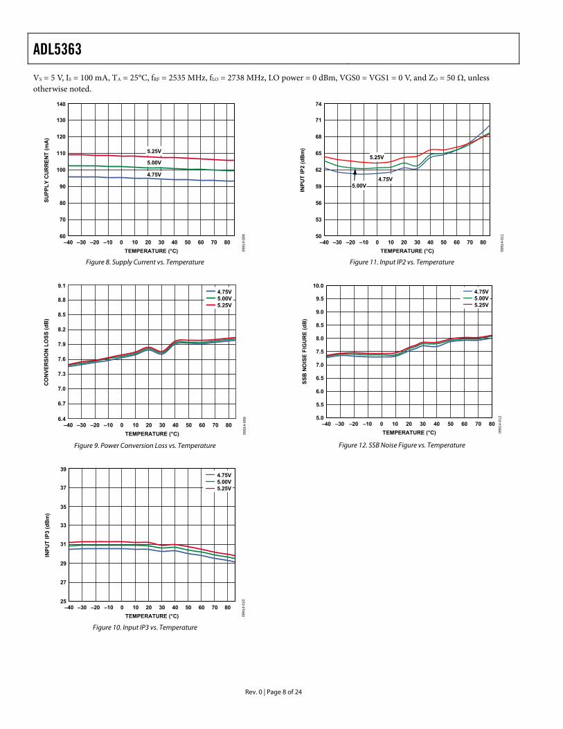
VS = 5 V, IS = 100 mA, TA = 25°C, fRF = 2535 MHz, fLO = 2738 MHz, LO power = 0 dBm, VGS0 = VGS1 = 0 V, and ZO = 50 Ω, unless otherwise noted.
140
130
110
100
90
80
70
120
60–40 –30 –20 –10 0 10 20 30 8070605040
SUPP
LY C
UR
REN
T (m
A)
TEMPERATURE (°C) 0991
4-00
8
5.25V
5.00V
4.75V
Figure 8. Supply Current vs. Temperature
9.1
8.8
8.2
7.9
7.6
7.3
6.7
7.0
8.5
6.4–40 –30 –20 –10 0 10 20 30 8070605040
CO
NVE
RSI
ON
LO
SS (d
B)
TEMPERATURE (°C) 0991
4-00
9
4.75V5.00V5.25V
Figure 9. Power Conversion Loss vs. Temperature
39
35
33
31
29
27
37
25–40 –30 –20 –10 0 10 20 30 8070605040
INPU
T IP
3 (d
Bm
)
TEMPERATURE (°C) 0991
4-01
0
4.75V5.00V5.25V
Figure 10. Input IP3 vs. Temperature
74
71
65
62
59
56
53
68
50–40 –30 –20 –10 0 10 20 30 8070605040
INPU
T IP
2 (d
Bm
)
TEMPERATURE (°C) 0991
4-01
1
5.25V
4.75V5.00V
Figure 11. Input IP2 vs. Temperature
10.0
9.5
8.5
8.0
7.5
7.0
6.5
9.0
5.0
6.0
5.5
–40 –30 –20 –10 0 10 20 30 8070605040
SSB
NO
ISE
FIG
UR
E (d
B)
TEMPERATURE (°C) 0991
4-01
2
4.75V5.00V5.25V
Figure 12. SSB Noise Figure vs. Temperature
ADL5363
Rev. 0 | Page 9 of 24
VS = 5 V, IS = 100 mA, TA = 25°C, fRF = 2535 MHz, fLO = 2738 MHz, LO power = 0 dBm, VGS0 = VGS1 = 0 V, and ZO = 50 Ω, unless otherwise noted.
120
115
105
100
85
90
95
110
8030 80 130 180 230 280 430380330
SUPP
LY C
UR
REN
T (m
A)
IF FREQUENCY (MHz) 0991
4-01
3
TA = +85°C
TA = –40°C
TA = +25°C
Figure 13. Supply Current vs. IF Frequency
8.4
8.2
8.0
7.8
7.2
7.4
7.6
7.030 80 130 180 230 280 430380330
CO
NVE
RSI
ON
LO
SS (d
B)
IF FREQUENCY (MHz) 0991
4-01
4
TA = +85°C
TA = –40°C
TA = +25°C
Figure 14. Power Conversion Loss vs. IF Frequency
41
38
35
32
23
26
29
2030 80 130 180 230 280 430380330
INPU
T IP
3 (d
Bm
)
IF FREQUENCY (MHz) 0991
4-01
5
TA = +85°C
TA = –40°C
TA = +25°C
Figure 15. Input IP3 vs. IF Frequency
100
90
80
70
50
60
4030 80 130 180 230 280 430380330
INPU
T IP
2 (d
Bm
)
IF FREQUENCY (MHz) 0991
4-01
6
TA = +85°C
TA = +25°C
TA = –40°C
Figure 16. Input IP2 vs. IF Frequency
10.0
9.5
9.0
7.5
7.0
6.5
8.0
8.5
6.030 80 130 180 230 280 430380330
SSB
NO
ISE
FIG
UR
E (d
B)
IF FREQUENCY (MHz) 0991
4-01
7
Figure 17. SSB Noise Figure vs. IF Frequency
ADL5363
Rev. 0 | Page 10 of 24
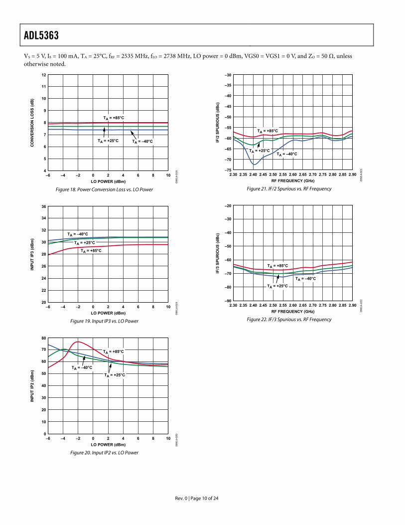
VS = 5 V, IS = 100 mA, TA = 25°C, fRF = 2535 MHz, fLO = 2738 MHz, LO power = 0 dBm, VGS0 = VGS1 = 0 V, and ZO = 50 Ω, unless otherwise noted.
12
10
11
8
9
7
6
5
4–6 –4 –2 0 2 4 6 8 10
CO
NVE
RSI
ON
LO
SS (d
B)
LO POWER (dBm) 0991
4-01
8
TA = –40°CTA = +25°C
TA = +85°C
Figure 18. Power Conversion Loss vs. LO Power
36
34
32
30
28
26
24
22
20–6 –4 –2 0 2 4 6 8 10
INPU
T IP
3 (d
Bm
)
LO POWER (dBm) 0991
4-01
9
TA = –40°C
TA = +25°C
TA = +85°C
Figure 19. Input IP3 vs. LO Power
80
70
60
50
40
30
20
10
0–6 –4 –2 0 2 4 6 8 10
INPU
T IP
2 (d
Bm
)
LO POWER (dBm) 0991
4-02
0
TA = –40°C
TA = +25°C
TA = +85°C
Figure 20. Input IP2 vs. LO Power
–30
–35
–40
–45
–50
–55
–60
–65
–70
–752.30 2.35 2.40 2.45 2.50 2.55 2.60 2.65 2.902.852.802.752.70
IF/2
SPU
RIO
US
(dB
c)
RF FREQUENCY (GHz) 0991
4-02
1
TA = –40°C
TA = +85°C
TA = +25°C
Figure 21. IF/2 Spurious vs. RF Frequency
–20
–30
–40
–50
–60
–70
–80
–902.30 2.35 2.40 2.45 2.50 2.55 2.60 2.65 2.902.852.802.752.70
IF/3
SPU
RIO
US
(dB
c)
RF FREQUENCY (GHz) 0991
4-02
2
TA = –40°C
TA = +85°C
TA = +25°C
Figure 22. IF/3 Spurious vs. RF Frequency
ADL5363
Rev. 0 | Page 11 of 24
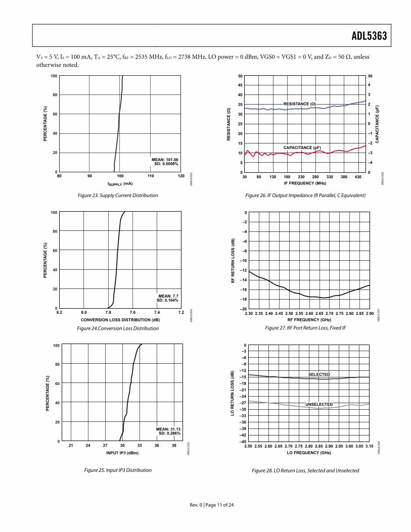
VS = 5 V, IS = 100 mA, TA = 25°C, fRF = 2535 MHz, fLO = 2738 MHz, LO power = 0 dBm, VGS0 = VGS1 = 0 V, and ZO = 50 Ω, unless otherwise noted.
PER
CEN
TAG
E (%
)
ISUPPLY (mA)
12011010080 90
100
80
60
40
20
0
0991
4-02
3
MEAN: 101.06SD: 0.0008%
Figure 23. Supply Current Distribution
PER
CEN
TAG
E (%
)
CONVERSION LOSS DISTRIBUTION (dB)
7.27.6 7.47.88.2 8.0
100
80
60
40
20
0
0991
4-02
4
MEAN: 7.7SD: 0.104%
Figure 24.Conversion Loss Distribution
PER
CEN
TAG
E (%
)
INPUT IP3 (dBm)
3930 33 362721 24
100
80
60
40
20
0
0991
4-02
5
MEAN: 31.13SD: 0.286%
Figure 25. Input IP3 Distribution
50
0
50
030 430
RES
ISTA
NC
E (Ω
)
CA
PAC
ITA
NC
E (p
F)
IF FREQUENCY (MHz) 0991
4-02
6
–4
–3
–2
–1
0
1
2
3
4
5
10
15
20
25
30
35
40
45
80 130 180 230 280 330 380
RESISTANCE (Ω)
CAPACITANCE (pF)
Figure 26. IF Output Impedance (R Parallel, C Equivalent)
0
–2
–4
–6
–10
–12
–14
–16
–18
–8
–202.30 2.35 2.40 2.45 2.50 2.55 2.60 2.65 2.902.852.802.752.70
RF
RET
UR
N L
OSS
(dB
)
RF FREQUENCY (GHz) 0991
4-02
7
Figure 27. RF Port Return Loss, Fixed IF
0
–452.50 3.10
LO R
ETU
RN
LO
SS (d
B)
LO FREQUENCY (GHz) 0991
4-02
8
–42–39–36–33–30–27–24–21–18–15–12
–9–6–3
2.55 2.60 2.65 2.70 2.75 2.80 2.85 2.90 2.95 3.00 3.05
SELECTED
UNSELECTED
Figure 28. LO Return Loss, Selected and Unselected
ADL5363
Rev. 0 | Page 12 of 24
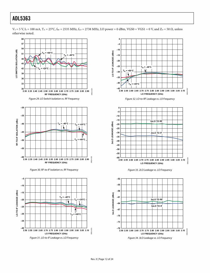
VS = 5 V, IS = 100 mA, TA = 25°C, fRF = 2535 MHz, fLO = 2738 MHz, LO power = 0 dBm, VGS0 = VGS1 = 0 V, and ZO = 50 Ω, unless otherwise noted.
60
57
54
51
48
45
42
39
36
33
302.30 2.35 2.40 2.45 2.50 2.55 2.60 2.65 2.902.852.802.752.70
LO S
WIT
CH
ISO
LATI
ON
(dB
)
RF FREQUENCY (GHz) 0991
4-02
9
TA = +85°CTA = –40°C
TA = +25°C
Figure 29. LO Switch Isolation vs. RF Frequency
–30
–35
–40
–45
–55
–50
–602.30 2.35 2.40 2.45 2.50 2.55 2.60 2.65 2.902.852.802.752.70
RF-
TO-IF
ISO
LATI
ON
(dB
c)
RF FREQUENCY (GHz) 0991
4-03
0
TA = –40°C
TA = +85°C
TA = +25°C
Figure 30. RF-to-IF Isolation vs. RF Frequency
–5
–10
–15
–20
–25
–30
–35
–402.50 2.55 2.60 2.65 2.70 2.75 2.80 3.103.00 3.052.952.902.85
LO-T
O-IF
LEA
KA
GE
(dB
m)
LO FREQUENCY (GHz) 0991
4-03
1
TA = +85°C
TA = –40°CTA = +25°C
Figure 31. LO-to-IF Leakage vs. LO Frequency
0
–5
–10
–15
–20
–25
–30
–35
–40
–452.50 2.55 2.60 2.65 2.70 2.75 2.80 3.103.00 3.052.952.902.85
LO-T
O-IF
LEA
KA
GE
(dB
m)
LO FREQUENCY (GHz) 0991
4-03
2
TA = +85°C
TA = –40°C
TA = +25°C
Figure 32. LO-to-RF Leakage vs. LO Frequency
0
–5
–10
–15
–20
–25
–30
–60
–55
–50
–45
–40
–35
2xLO
LEA
KA
GE
(dB
m)
0991
4-03
3
2xLO TO RF
2xLO TO IF
2.50 3.10LO FREQUENCY (GHz)
2.55 2.60 2.65 2.70 2.75 2.80 2.85 2.90 2.95 3.00 3.05
Figure 33. 2LO Leakage vs. LO Frequency
–52
–55
–58
–61
–76
–67
–70
–73
–64
2.50 2.55 2.60 2.65 2.70 2.75 2.80 2.85 2.90 2.95 3.00 3.05 3.10
3xLO
LEA
KA
GE
(dB
m)
LO FREQUENCY (GHz) 0991
4-03
4
3xLO TO RF
3xLO TO IF
Figure 34. 3LO Leakage vs. LO Frequency
ADL5363
Rev. 0 | Page 13 of 24
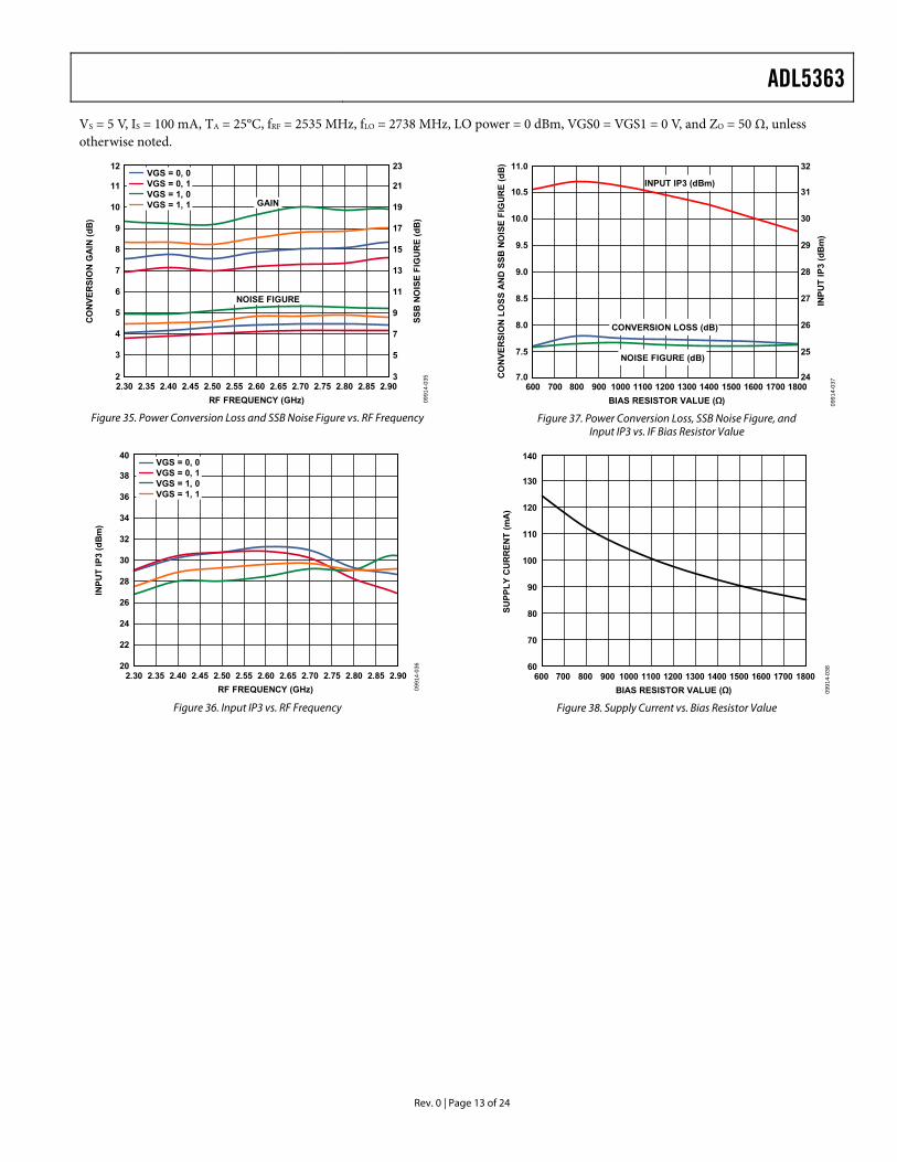
VS = 5 V, IS = 100 mA, TA = 25°C, fRF = 2535 MHz, fLO = 2738 MHz, LO power = 0 dBm, VGS0 = VGS1 = 0 V, and ZO = 50 Ω, unless otherwise noted.
12
11
10
9
8
7
6
5
4
3
22.30 2.35 2.40 2.45 2.50 2.55 2.60 2.65 2.902.852.802.752.70
CO
NVE
RSI
ON
GA
IN (d
B)
RF FREQUENCY (GHz) 0991
4-03
5
23
3
7
5
9
11
13
15
17
19
21
SSB
NO
ISE
FIG
UR
E (d
B)
VGS = 0, 0VGS = 0, 1VGS = 1, 0VGS = 1, 1 GAIN
NOISE FIGURE
Figure 35. Power Conversion Loss and SSB Noise Figure vs. RF Frequency
40
38
36
34
30
28
26
24
22
32
202.30 2.35 2.40 2.45 2.50 2.55 2.60 2.65 2.902.852.802.752.70
INPU
T IP
3(d
Bm
)
RF FREQUENCY (GHz) 0991
4-03
6
VGS = 0, 0VGS = 0, 1VGS = 1, 0VGS = 1, 1
Figure 36. Input IP3 vs. RF Frequency
11.0
10.5
10.0
9.5
9.0
8.5
8.0
7.5
7.0
32
31
30
29
28
27
26
25
24600 700 900800 1000 1100 1200 1300 1400 1500 1600 1700 1800
CO
NVE
RSI
ON
LOSS
AN
DSS
BN
OIS
EFI
GU
RE
(dB
)
INPU
T IP
3(d
Bm
)
BIAS RESISTOR VALUE (Ω) 0991
4-03
7
CONVERSION LOSS (dB)
NOISE FIGURE (dB)
INPUT IP3 (dBm)
Figure 37. Power Conversion Loss, SSB Noise Figure, and
Input IP3 vs. IF Bias Resistor Value
140
130
120
110
100
90
80
70
60600 1800
SUPP
LY C
UR
REN
T (m
A)
BIAS RESISTOR VALUE (Ω) 0991
4-03
8
700 900800 1000 1100 1200 1300 1400 1500 1600 1700
Figure 38. Supply Current vs. Bias Resistor Value
ADL5363
Rev. 0 | Page 14 of 24
3.3 V PERFORMANCE VS = 3.3 V, IS = 60 mA, TA = 25°C, fRF = 2535 MHz, fLO = 2738 MHz, LO power = 0 dBm, VGS0 = VGS1 = 0 V, and ZO = 50 Ω, unless otherwise noted.
67
65
63
61
57
59
562.30 2.35 2.40 2.45 2.50 2.55 2.60 2.65 2.902.852.802.752.70
SUPP
LY C
UR
REN
T (m
A)
RF FREQUENCY (GHz) 0991
4-03
9
TA = +25°CTA = –40°C
TA = +85°C
Figure 39. Supply Current vs. RF Frequency at 3.3 V
9.0
8.5
8.0
7.5
7.0
6.5
5.0
5.5
6.0
2.30 2.35 2.40 2.45 2.50 2.55 2.60 2.65 2.902.852.802.752.70
CO
NVE
RSI
ON
LO
SS (d
B)
RF FREQUENCY (GHz) 0991
4-04
0
TA = +85°C
TA = –40°CTA = +25°C
Figure 40. Power Conversion Loss vs. RF Frequency at 3.3 V
34
31
28
25
22
19
10
13
16
2.30 2.35 2.40 2.45 2.50 2.55 2.60 2.65 2.902.852.802.752.70
INPU
T IP
3 (d
Bm
)
RF FREQUENCY (GHz) 0991
4-04
1
TA = +85°C
TA = –40°C
TA = +25°C
Figure 41. Input IP3 vs. RF Frequency at 3.3 V
100
90
80
70
60
50
20
30
40
2.30 2.35 2.40 2.45 2.50 2.55 2.60 2.65 2.902.852.802.752.70
INPU
T IP
2 (d
Bm
)
RF FREQUENCY (GHz) 0991
4-04
2
TA = –40°C
TA = +85°C
TA = +25°C
Figure 42. Input IP2 vs. RF Frequency at 3.3 V
9.0
8.5
8.0
7.0
7.5
4.0
4.5
5.0
5.5
6.0
6.5
2.30 2.35 2.40 2.45 2.50 2.55 2.60 2.65 2.902.852.802.752.70
SSB
NO
ISE
FIG
UR
E (d
B)
FREQUENCY (GHz) 0991
4-04
3
TA = –40°C
TA = +85°C
TA = +25°C
Figure 43. SSB Noise Figure vs. RF Frequency at 3.3 V
ADL5363
Rev. 0 | Page 15 of 24
UPCONVERSION VS = 5 V, IS = 100 mA, TA = 25°C, fRF = 2535 MHz, fLO = 2738 MHz, LO power = 0 dBm, VGS0 = VGS1 = 0 V, and ZO = 50 Ω, unless otherwise noted.
13
12
11
10
9
8
7
6
5
4
32.30 2.35 2.40 2.45 2.50 2.55 2.60 2.65 2.902.852.802.752.70
CO
NVE
RSI
ON
LO
SS (d
B)
RF FREQUENCY (GHz) 0991
4-04
4
TA = +85°C
TA = –40°C
TA = +25°C
Figure 44. Power Conversion Loss vs. RF Frequency, VS = 5 V, Upconversion
30
29
28
27
26
25
24
23
22
21
202.30 2.35 2.40 2.45 2.50 2.55 2.60 2.65 2.902.852.802.752.70
INPU
T IP
3 (d
Bm
)
RF FREQUENCY (GHz) 0991
4-04
5
TA = +25°C
TA = +85°C
TA = –40°C
Figure 45. Input IP3 vs. RF Frequency, VS = 5 V, Upconversion
9.0
8.5
8.0
7.5
7.0
6.5
5.5
6.0
5.0
4.5
4.02.30 2.35 2.40 2.45 2.50 2.55 2.60 2.65 2.902.852.802.752.70
CO
NVE
RSI
ON
LO
SS (d
B)
RF FREQUENCY (GHz) 0991
4-04
6
TA = +25°C
TA = –40°C
TA = +85°C
Figure 46. Power Conversion Loss vs. RF Frequency at 3.3 V, Upconversion
35
33
31
29
27
25
21
23
19
17
152.30 2.35 2.40 2.45 2.50 2.55 2.60 2.65 2.902.852.802.752.70
INPU
T IP
3 (d
Bm
)
RF FREQUENCY (GHz) 0991
4-04
7
TA = –40°C
TA = +85°C
TA = +25°C
Figure 47. Input IP3 vs. RF Frequency at 3.3 V, Upconversion
ADL5363
Rev. 0 | Page 16 of 24
SPURIOUS PERFORMANCE (N × fRF) − (M × fLO) spur measurements were made using the standard evaluation board. Mixer spurious products are measured in dBc from the IF output power level. Data was measured only for frequencies less than 6 GHz. Typical noise floor of the measurement system = −100 dBm.
5 V Performance
VS = 5 V, IS = 100 mA, TA = 25°C, fRF = 2535 MHz, fLO = 2738 MHz, LO power = 0 dBm, RF power = 0 dBm, VGS0 = VGS1 = 0 V, and ZO = 50 Ω, unless otherwise noted.
M
0 1 2 3 4 5 6 7 8 9 10 11 12 13 14 15
0 −10.9 −28.3 −44.5
1 −42.2 0.0 −49.3 −31.2 −49.8
2 −75.8 −76.5 −64.6 −78.4 −78.5 −94.7
3 <−100 −83.0 <−100 −73.5 −90.9 −89.8 <−100
4 <−100 <−100 <−100 <−100 <−100 <−100 <−100 <−100
5 <−100 <−100 <−100 <−100 <−100 <−100 <−100
6 <−100 <−100 <−100 <−100 <−100 <−100 <−100
7 <−100 <−100 <−100 <−100 <−100 <−100 <−100
8 <−100 <−100 <−100 <−100 <−100 <−100 <−100
9 <−100 <−100 <−100 <−100 <−100 <−100 <−100
10 <−100 <−100 <−100 <−100 <−100 <−100 <−100
11 <−100 <−100 <−100 <−100 <−100 <−100 <−100
12 <−100 <−100 <−100 <−100 <−100 <−100
13 <−100 <−100 <−100 <−100
14 <−100 <−100 <−100
N
15 <−100 <−100
3.3 V Performance
VS = 3.3 V, IS = 56 mA, TA = 25°C, fRF = 2535 MHz, fLO = 2738 MHz, LO power = 0 dBm, RF power = 0 dBm, R9 = 226 Ω, VGS0 = VGS1 = 0 V, and ZO = 50 Ω, unless otherwise noted.
M
0 1 2 3 4 5 6 7 8 9 10 11 12 13 14 15
0 −16.9 −35.1 −61.4
1 −41.9 0.0 −49.1 −30.4 −52.6
2 −72.3 −80.3 −62.7 −68.5 −71.9 <−100
3 −94.6 −71.6 <−100 −61.2 −92.7 −75.1 <−100
4 <−100 <−100 <−100 <−100 <−100 <−100 <−100 <−100
5 <−100 <−100 <−100 <−100 <−100 <−100 <−100
6 <−100 <−100 <−100 <−100 <−100 <−100 <−100
7 <−100 <−100 <−100 <−100 <−100 <−100 <−100
8 <−100 <−100 <−100 <−100 <−100 <−100 <−100
9 <−100 <−100 <−100 <−100 <−100 <−100 <−100
10 <−100 <−100 <−100 <−100 <−100 <−100 <−100
11 <−100 <−100 <−100 <−100 <−100 <−100 <−100
12 <−100 <−100 <−100 <−100 <−100 <−100
13 <−100 <−100 <−100 <−100
14 <−100 <−100 <−100
N
15 <−100
ADL5363
Rev. 0 | Page 17 of 24
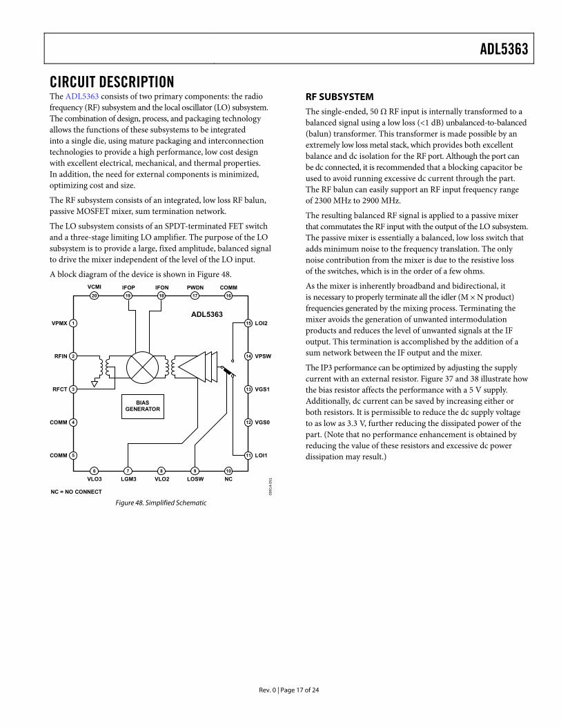
CIRCUIT DESCRIPTION RF SUBSYSTEM The ADL5363 consists of two primary components: the radio
frequency (RF) subsystem and the local oscillator (LO) subsystem. The combination of design, process, and packaging technology allows the functions of these subsystems to be integrated into a single die, using mature packaging and interconnection technologies to provide a high performance, low cost design with excellent electrical, mechanical, and thermal properties. In addition, the need for external components is minimized, optimizing cost and size.
The single-ended, 50 Ω RF input is internally transformed to a balanced signal using a low loss (<1 dB) unbalanced-to-balanced (balun) transformer. This transformer is made possible by an extremely low loss metal stack, which provides both excellent balance and dc isolation for the RF port. Although the port can be dc connected, it is recommended that a blocking capacitor be used to avoid running excessive dc current through the part. The RF balun can easily support an RF input frequency range of 2300 MHz to 2900 MHz. The RF subsystem consists of an integrated, low loss RF balun,
passive MOSFET mixer, sum termination network. The resulting balanced RF signal is applied to a passive mixer that commutates the RF input with the output of the LO subsystem. The passive mixer is essentially a balanced, low loss switch that adds minimum noise to the frequency translation. The only noise contribution from the mixer is due to the resistive loss of the switches, which is in the order of a few ohms.
The LO subsystem consists of an SPDT-terminated FET switch and a three-stage limiting LO amplifier. The purpose of the LO subsystem is to provide a large, fixed amplitude, balanced signal to drive the mixer independent of the level of the LO input.
A block diagram of the device is shown in Figure 48. As the mixer is inherently broadband and bidirectional, it is necessary to properly terminate all the idler (M × N product) frequencies generated by the mixing process. Terminating the mixer avoids the generation of unwanted intermodulation products and reduces the level of unwanted signals at the IF output. This termination is accomplished by the addition of a sum network between the IF output and the mixer. 2
3
1
20 19 18 17 16
6 7 8 9 10
4
5
14
13
15
12
BIASGENERATOR
VPMX
RFIN
RFCT
COMM
COMM
LOI2
VPSW
VGS1
VGS0
LOI1
VCMI IFOP IFON PWDN COMM
VLO3 LGM3 VLO2 LOSW NC
ADL5363
NC = NO CONNECT
11
0991
4-05
1
The IP3 performance can be optimized by adjusting the supply current with an external resistor. Figure 37 and 38 illustrate how the bias resistor affects the performance with a 5 V supply. Additionally, dc current can be saved by increasing either or both resistors. It is permissible to reduce the dc supply voltage to as low as 3.3 V, further reducing the dissipated power of the part. (Note that no performance enhancement is obtained by reducing the value of these resistors and excessive dc power dissipation may result.)
Figure 48. Simplified Schematic
ADL5363
Rev. 0 | Page 18 of 24
LO SUBSYSTEM The ADL5363 has two LO inputs permitting multiple synthesizers to be rapidly switched with extremely short switching times (<40 ns) for frequency agile applications. The two inputs are applied to a high isolation SPDT switch that provides a constant input impedance, regardless of whether the port is selected, to avoid pulling the LO sources. This multiple section switch also ensures high isolation to the off input, minimizing any leakage from the unwanted LO input that may result in undesired IF responses.
The single-ended LO input is converted to a fixed amplitude differential signal using a multistage, limiting LO amplifier. This results in consistent performance over a range of LO input power. Optimum performance is achieved from −6 dBm to +10 dBm, but the circuit continues to function at considerably lower levels of LO input power.
The performance of this amplifier is critical in achieving a high intercept passive mixer without degrading the noise floor of the system. This is a critical requirement in an interferer rich environment, such as cellular infrastructure, where blocking
interferers can limit mixer performance. The bandwidth of the intermodulation performance is somewhat influenced by the current in the LO amplifier chain. For dc current sensitive applications, it is permissible to reduce the current in the LO amplifier by raising the value of the external bias control resistor. For dc current critical applications, the LO chain can operate with a supply voltage as low as 3.3 V, resulting in substantial dc power savings.
In addition, when operating with supply voltages below 3.6 V, the ADL5363 has a power-down mode that permits the dc current to drop to <200 μA.
All of the logic inputs are designed to work with any logic family that provides a Logic 0 input level of less than 0.4 V and a Logic 1 input level that exceeds 1.4 V. All logic inputs are high impedance up to Logic 1 levels of 3.3 V. At levels exceeding 3.3 V, protection circuitry permits operation up to 5.5 V, although a small bias current is drawn.
All pins, including the RF pins, are ESD protected and have been tested up to a level of 1500 V HBM and 1250 V CDM.
ADL5363
Rev. 0 | Page 19 of 24
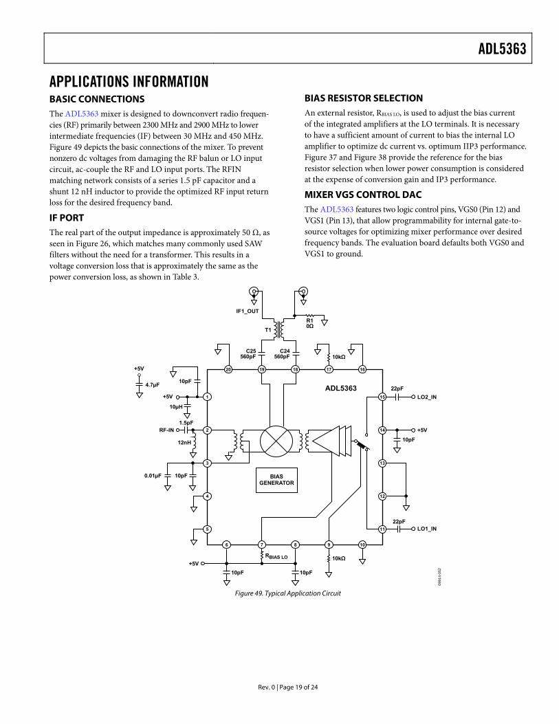
APPLICATIONS INFORMATION BASIC CONNECTIONS The ADL5363 mixer is designed to downconvert radio frequen-cies (RF) primarily between 2300 MHz and 2900 MHz to lower intermediate frequencies (IF) between 30 MHz and 450 MHz. Figure 49 depicts the basic connections of the mixer. To prevent nonzero dc voltages from damaging the RF balun or LO input circuit, ac-couple the RF and LO input ports. The RFIN matching network consists of a series 1.5 pF capacitor and a shunt 12 nH inductor to provide the optimized RF input return loss for the desired frequency band.
IF PORT The real part of the output impedance is approximately 50 Ω, as seen in Figure 26, which matches many commonly used SAW filters without the need for a transformer. This results in a voltage conversion loss that is approximately the same as the power conversion loss, as shown in Table 3.
BIAS RESISTOR SELECTION An external resistor, RBIAS LO, is used to adjust the bias current of the integrated amplifiers at the LO terminals. It is necessary to have a sufficient amount of current to bias the internal LO amplifier to optimize dc current vs. optimum IIP3 performance. Figure 37 and Figure 38 provide the reference for the bias resistor selection when lower power consumption is considered at the expense of conversion gain and IP3 performance.
MIXER VGS CONTROL DAC The ADL5363 features two logic control pins, VGS0 (Pin 12) and VGS1 (Pin 13), that allow programmability for internal gate-to-source voltages for optimizing mixer performance over desired frequency bands. The evaluation board defaults both VGS0 and VGS1 to ground.
2
3
1
19 18 17 16
6 7 8 9 10
14
15
12
11
BIASGENERATOR
LO2_IN
RF-IN +5V
+5V
+5V
+5V
LO1_IN
10kΩ
R10Ω
C24560pF
10kΩ
10pF10pF
10pF
1.5pF
10pF
10µH
0.01µF
4.7µF
RBIAS LO
22pF
10pF
22pF
ADL5363
20
13
5
4
0991
4-05
2
T1
IF1_OUT
C25560pF
12nH
Figure 49. Typical Application Circuit
ADL5363
Rev. 0 | Page 20 of 24
EVALUATION BOARD An evaluation board is available for the family of double balanced mixers. The standard evaluation board schematic is shown in Figure 50. The evaluation board is fabricated using Rogers® RO3003 material. Table 7 describes the various configuration options of the evaluation board. Evaluation board layout is shown in Figure 51 to Figure 54.
0991
4-05
3
C221nF
C2010pF
C210µF
C2110pF
C11.5pF
C1022pF
C1222pF
VGS1
LO2_IN
LO1_IN
RF-IN
R2210kΩ
VPOS
PWR_UP
R2315kΩ
VPOS
VPOS
VPOS
LOSEL
VGS0
C50.01µF
C410pF
C610pF
C810pF
R91.1kΩ
R410kΩ
R2110kΩR14
0ΩL30Ω
VPMX
RFIN
RFCT
COMM
COMM
VGS1
VPSW
LOI2
VGS0
LOI1
IFO
N
IFO
P
VCM
I
PWD
N
CO
MM
VLO
3
LGM
3
VLO
2
NC
LOSW
ADL5363
R10Ω
C24560pF
T1
IF1_OUT
C25560pF
Z112nH
Figure 50. Evaluation Board Schematic
ADL5363
Rev. 0 | Page 21 of 24
Table 7. Evaluation Board Configuration Components Function Description Default Conditions C2, C6, C8, C20, C21
Power supply decoupling
Power Supply Decoupling. Nominal supply decoupling consists of a 10 μF capacitor to ground in parallel with a 10 pF capacitor to ground positioned as close to the device as possible.
C2 = 10 μF (size 0603), C6, C8, C20, C21 = 10 pF (size 0402)
C1, C4, C5, Z1 RF input interface RF Input Interface. The input channels are ac-coupled through C1. C4 and C5 provide bypassing for the center taps of the RF input baluns.
C1 = 1.5 pF (size 0402), C4 = 10 pF (size 0402), C5 = 0.01 μF (size 0402) Z1= 12 nH (size 0402)
T1, R1, C24, C25 IF output interface IF Output Interface. T1 is a 1:1 impedance transformer used to provide a single-ended IF output interface. Remove R1 for balanced output operation. C24 and C25 are used to block the dc bias at the IF ports.
T1 = TC1-1-13M+ (Mini-Circuits), R1 = 0 Ω (size 0402), C24, C25 = 560 pF (size 0402)
C10, C12, R4 LO interface LO Interface. C10 and C12 provide ac coupling for the LO1_IN and LO2_IN local oscillator inputs. LOSEL selects the appropriate LO input for both mixer cores. R4 provides a pull-down to ensure that LO1_IN is enabled when the LOSEL test point is logic low. LO2_IN is enabled when LOSEL is pulled to logic high.
C10, C12 = 22 pF (size 0402), R4 = 10 kΩ (size 0402)
R21 PWDN interface PWDN Interface. R21 pulls the PWDN logic low and enables the device. The PWR_UP test point allows the PWDN interface to be exercised using the an external logic generator. Grounding the PWDN pin for nominal operation is allowed. Using the PWDN pin when supply voltages exceed 3.3 V is not allowed.
R21 = 10 kΩ (size 0402)
C22, L3, R9, R14, R22, R23, VGS0, VGS1
Bias control Bias Control. R22 and R23 form a voltage divider to provide 3 V for logic control, bypassed to ground through C22. VGS0 and VGS1 jumpers provide programmability at the VGS0 and VGS1 pins. It is recommended to pull these two pins to ground for nominal operation. R9 sets the bias point for the internal LO buffers.
C22 = 1 nF (size 0402), L3 = 0 Ω (size 0603), R9 = 1.1 kΩ (size 0402), R14 = 0 Ω (size 0402), R22 = 10 kΩ (size 0402), R23 = 15 kΩ (size 0402), VGS0 = VGS1 = 3-pin shunt
ADL5363
Rev. 0 | Page 22 of 24
0991
4-15
2
Figure 51. Evaluation Board Top Layer
0991
4-15
3
Figure 52. Evaluation Board Ground Plane, Internal Layer 1
0991
4-15
4
Figure 53. Evaluation Board Power Plane, Internal Layer 2
0991
4-15
5
Figure 54. Evaluation Board Bottom Layer
ADL5363
Rev. 0 | Page 23 of 24
OUTLINE DIMENSIONS
COMPLIANT TOJEDEC STANDARDS MO-220-VHHC 0422
09-B
10.65BSC
PIN 1INDICATOR
2.60 BSC
0.750.600.50
TOP VIEW
12° MAX
SEATINGPLANE
PIN 1INDICATOR
COPLANARITY0.05
0.900.850.80
0.350.280.23
0.05 MAX0.01 NOM
0.20 REF
0.700.650.60
3.203.10 SQ3.00
20
6
16
1011
15
5
EXPOSEDPAD
(BOTTOM VIEW)
0.60 MAX
0.60 MAX
5.00BSC SQ
4.75BSC SQ
FOR PROPER CONNECTION OFTHE EXPOSED PAD, REFER TOTHE PIN CONFIGURATION ANDFUNCTION DESCRIPTIONSSECTION OF THIS DATA SHEET.
Figure 55. 20-Lead Lead Frame Chip Scale Package [LFCSP_VQ]
5 mm × 5 mm Body, Very Thin Quad (CP-20-5)
Dimensions shown in millimeters
ORDERING GUIDE Model1 Temperature Range Package Description Package Option Ordering Quantity ADL5363ACPZ-R7 −40°C to +85°C 20-Lead Lead Frame Chip Scale Package [LFCSP_VQ]
7” Tape and Reel CP-20-5 1,500
ADL5363-EVALZ Evaluation Board 1 1 Z = RoHS Compliant Part.

ADL5363
Rev. 0 | Page 24 of 24
NOTES
©2011 Analog Devices, Inc. All rights reserved. Trademarks and registered trademarks are the property of their respective owners. D09914-0-7/11(0)