2.2.0 - intel 80186 hardware operation lecture-2008
TRANSCRIPT
ECE – 684HW Operation
Intel 80186 Hardware Operation
1
ECE – 684HW Operation
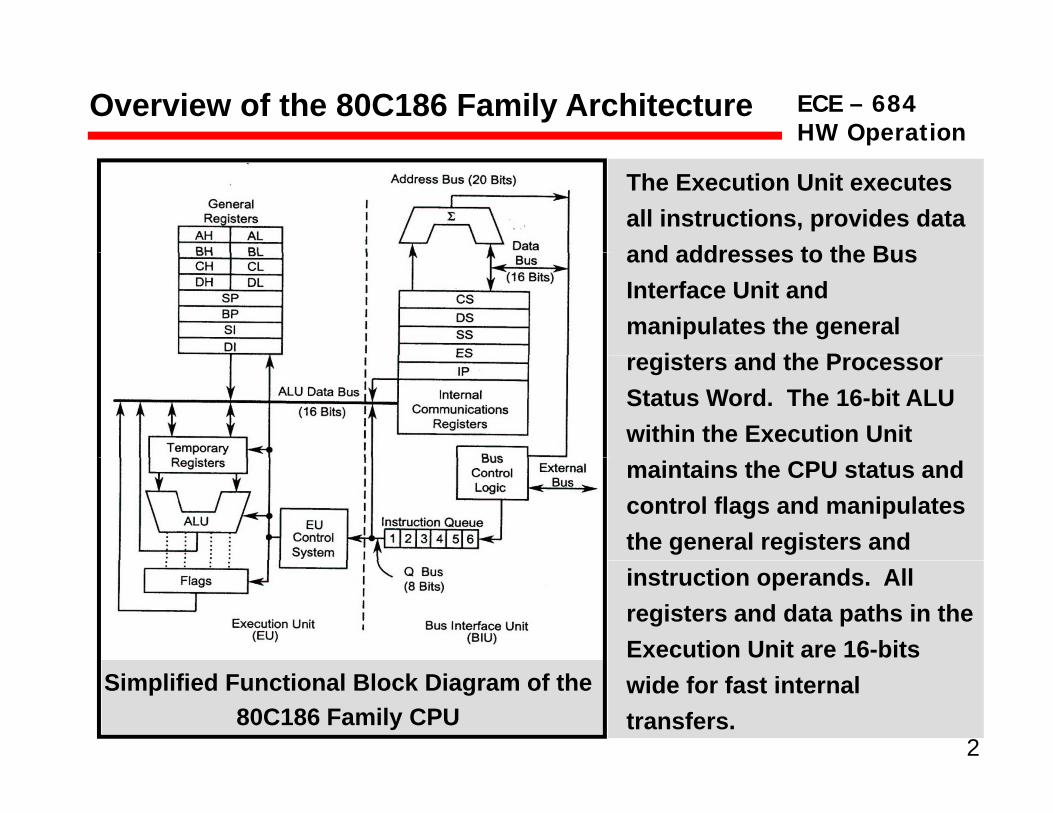
Overview of the 80C186 Family Architecture
The Execution Unit executes all instructions, provides data and addresses to the Busand addresses to the Bus Interface Unit and manipulates the general
i t d th Pregisters and the Processor Status Word. The 16-bit ALU within the Execution Unit maintains the CPU status and control flags and manipulates the general registers and instruction operands. All registers and data paths in the Execution Unit are 16-bits
2
wide for fast internal transfers.
Simplified Functional Block Diagram of the 80C186 Family CPU

ECE – 684HW Operation
8086 CPU Block Diagram
3
ECE – 684HW Operation
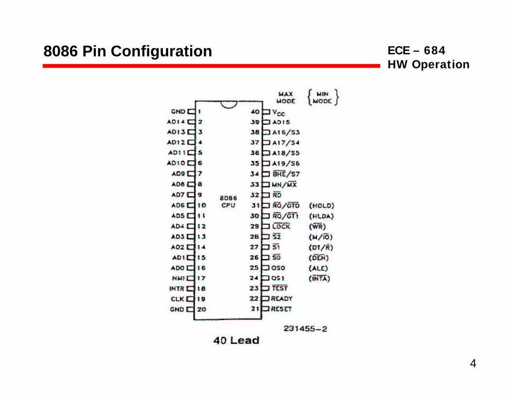
8086 Pin Configuration
4
ECE – 684HW Operation
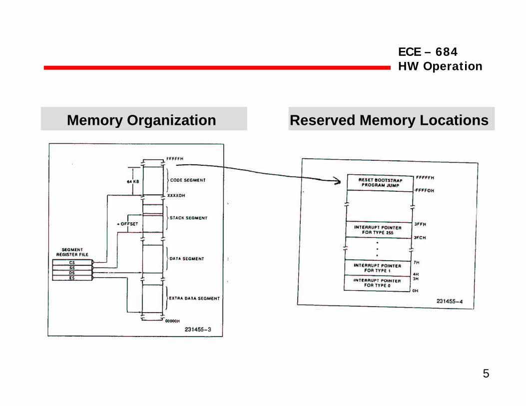
Memory Organization Reserved Memory Locationsy g y
5
ECE – 684HW Operation
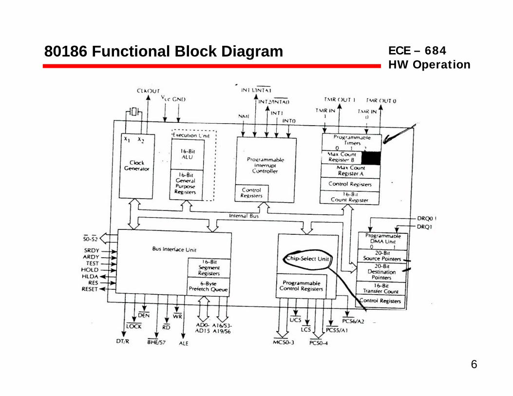
80186 Functional Block Diagram
6
ECE – 684HW Operation
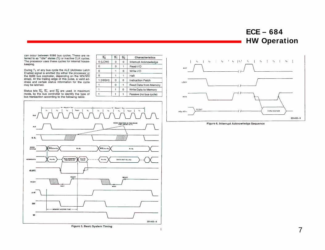
7
ECE – 684HW Operation
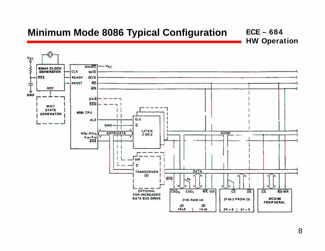
Minimum Mode 8086 Typical Configuration
8
ECE – 684HW Operation
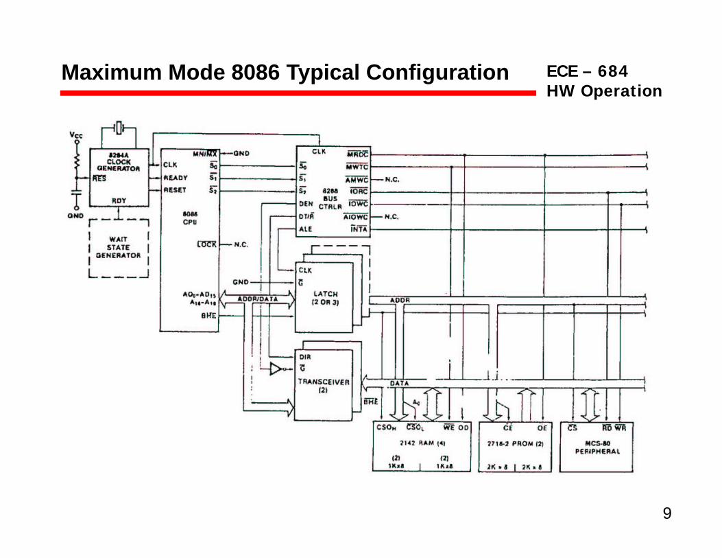
Maximum Mode 8086 Typical Configuration
9
ECE – 684HW Operation
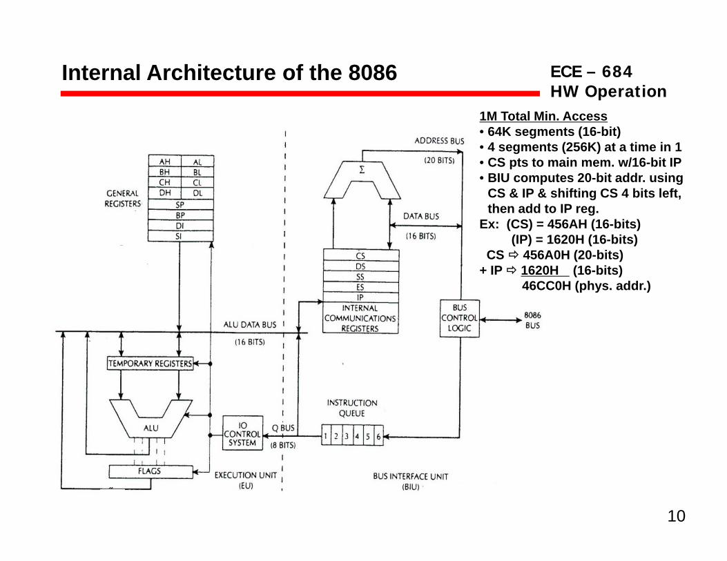
Internal Architecture of the 8086
1M Total Min. Access• 64K segments (16-bit)• 4 segments (256K) at a time in 1• CS pts to main mem. w/16-bit IP
BIU t 20 bit dd i• BIU computes 20-bit addr. using CS & IP & shifting CS 4 bits left, then add to IP reg.
Ex: (CS) = 456AH (16-bits)(IP) = 1620H (16-bits)( ) ( )
CS 456A0H (20-bits)+ IP 1620H (16-bits)
46CC0H (phys. addr.)
10
ECE – 684HW Operation
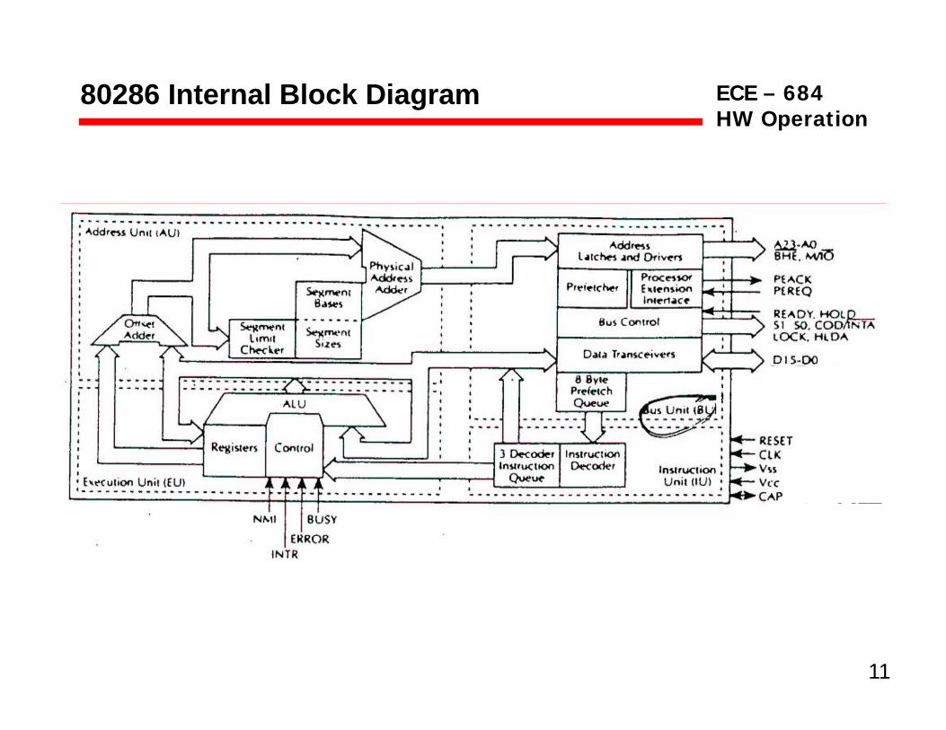
80286 Internal Block Diagram
11
ECE – 684HW Operation
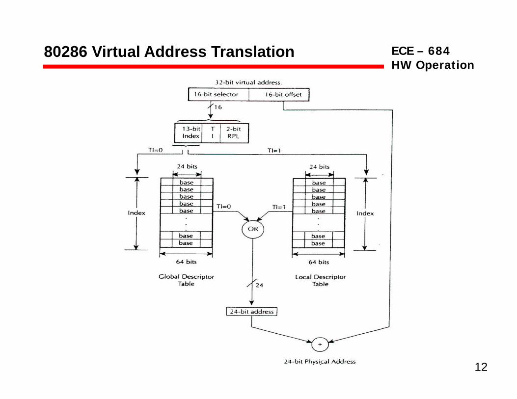
80286 Virtual Address Translation
12
ECE – 684HW Operation
80x87 Floating point coprocessor
When the 8086 CPU first appeared in the late 1970's, semiconductor technology was not to the point where Intel could put floating point instrutions directly on the 8086 CPU. Therefore, they devised a scheme whereby they could use a second chip to perform the floating point calculations - the floating point unit (or FPU)[6]. They released their original floating point chip, the 8087, in 1980. This particular FPU worked with the 8086, 8088, 80186, and 80188 CPUs. When Intel introduced the 80286 CPU, they released a redesigned 80287 FPU chip to accompany it. Although the 80287 was compatible with the 80386 CPU, Intel designed a better FPU, the 80387, for use in 80386 systems. The 80486 CPU was the first Intel CPU to include an on-chip floating point unit. Shortly after the release of the 80486, Intel introduced the 80486sx CPU that was an 80486 without the built-in FPU. To get floating point capabilities on this chip, you had to add an 80487 chip, although the 80487 was really nothing more than a full-blown 80486 which took over for the "sx" chip in the system. Intel's Pentium/586 chips provide a high-performance floating point unit directly on the CPU. There is no floating point coprocessor available for the Pentium chip.
13Source: Art of Assembly: Chapter Fourteen
ECE – 684HW Operation
80x87 FPU Regs
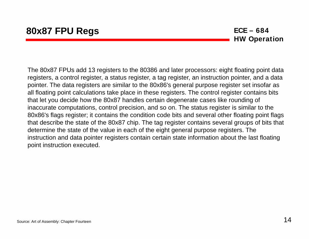
The 80x87 FPUs add 13 registers to the 80386 and later processors: eight floating point data registers, a control register, a status register, a tag register, an instruction pointer, and a data pointer. The data registers are similar to the 80x86's general purpose register set insofar as all floating point calculations take place in these registers. The control register contains bits that let you decide how the 80x87 handles certain degenerate cases like rounding of inaccurate computations, control precision, and so on. The status register is similar to the 80x86's flags register; it contains the condition code bits and several other floating point flags that describe the state of the 80x87 chip. The tag register contains several groups of bits that determine the state of the value in each of the eight general purpose registers. The instruction and data pointer registers contain certain state information about the last floating point instruction executed.
14Source: Art of Assembly: Chapter Fourteen

ECE – 684HW Operation
80x87 FPU Data Regs
The 80x87 FPUs provide eight 80 bit data registers organized as a stack. This is a significant departure from the organization of the general purpose registers on the 80x86 CPU that comprise a standard general-purpose register set. Intel refers to these registers as ST(0), co p se a sta da d ge e a pu pose eg ste set te e e s to t ese eg ste s as S (0),ST(1), ..., ST(7). Most assemblers will accept ST as an abbreviation for ST(0).
15Source: Art of Assembly: Chapter Fourteen
ECE – 684HW Operation
80x87 FPU Control Reg
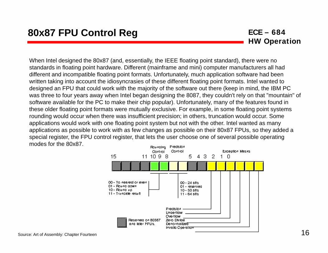
When Intel designed the 80x87 (and, essentially, the IEEE floating point standard), there were no standards in floating point hardware. Different (mainframe and mini) computer manufacturers all had different and incompatible floating point formats. Unfortunately, much application software had been written taking into account the idiosyncrasies of these different floating point formats. Intel wanted to designed an FPU that could work with the majority of the software out there (keep in mind, the IBM PC was three to four years away when Intel began designing the 8087, they couldn't rely on that "mountain" of software available for the PC to make their chip popular). Unfortunately, many of the features found in these older floating point formats were mutually exclusive. For example, in some floating point systemsthese older floating point formats were mutually exclusive. For example, in some floating point systems rounding would occur when there was insufficient precision; in others, truncation would occur. Some applications would work with one floating point system but not with the other. Intel wanted as many applications as possible to work with as few changes as possible on their 80x87 FPUs, so they added a special register, the FPU control register, that lets the user choose one of several possible operating
d f th 80 87modes for the 80x87.
16Source: Art of Assembly: Chapter Fourteen
ECE – 684HW Operation
80x87 FPU Status Reg
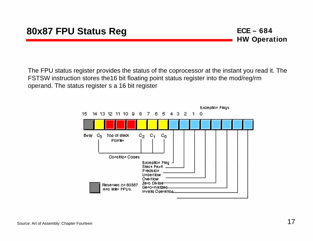
The FPU status register provides the status of the coprocessor at the instant you read it. The FSTSW instruction stores the16 bit floating point status register into the mod/reg/rm operand. The status register s a 16 bit register
17Source: Art of Assembly: Chapter Fourteen
ECE – 684HW Operation
80x87 FPU Data Types
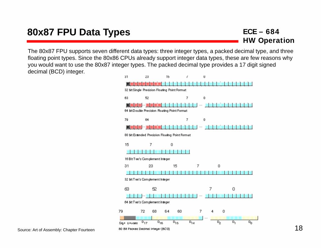
The 80x87 FPU supports seven different data types: three integer types, a packed decimal type, and three floating point types. Since the 80x86 CPUs already support integer data types, these are few reasons why you would want to use the 80x87 integer types. The packed decimal type provides a 17 digit signed decimal (BCD) integer.
18Source: Art of Assembly: Chapter Fourteen