2.1 boolean algebra: the logic of true and false
TRANSCRIPT

41
The work of computation is performed by millions of tiny electronic devices called digital logic gates, or just “gates.” These gates take binary inputs and produce binary outputs, zero or one, depending on the function the gate com-putes and the inputs applied to the gate. This chapter explores digital logic gates and shows how they are used for computation.
2.1 Boolean Algebra: The Logic of True and False
George Boole (1815 – 1864) was a British mathematician and philosopher. He made a number of important contributions to mathe-matics. The most important to those who study computing was the Boolean algebra, an algebra over finite sets of discrete values. Boole studied and wrote about propositions – statements which may be true or false – and operators like AND, OR, and NOT that connect them.
Think about two propositions:
a: it is midnight in the United States. b: the sun is not visible.
We can write the proposition as a ⇒ b which is read “a implies b.” Note that the reverse is not true in this case. The fact that the sun is not visible does not mean it is midnight.
Figure 2-1 George Boole
Copyright © 2020 by Bob Brown 2020-10-09 15:24
Please report errors to [email protected]

Computing Concepts for Information Technology
42
Propositions can be combined with logical operators, like this: a: A graduating grade point average of greater than 3.7 earns honors. b: Bill’s graduating GPA was 3.96. f: Bill has graduated with honors.
We can write f = a ∧ b where ∧ is the AND operator. Both a (the criterion for earning honors) and b (Bill’s graduating GPA being greater than 3.7) must be true for Bill to have graduated with honors. If Bill’s graduating GPA were 3.5, then f would be false; Bill did not graduate with honors.
A special case of Boolean algebra is the switching algebra, introduced by Claude Shannon in the late 1930s. In the switching algebra, variables can have only two possible values, true or false; the result of a function in the switching algebra can therefore only be true or false. Those involved with computing of-ten refer to the switching algebra as Boolean algebra, and so does this book. By considering true to be one and false to be zero, Boolean algebra, specifically the switching algebra, becomes an algebra over finite sets of binary numbers.
We can express the AND operator as f(a,b) = a•b where a•b is the Boolean prod-uct, or conjunction. This says that f(a,b) is one if and only if both a and b are one. We will use either the center-dot, a•b, or implicit multiplication, ab, in place of ∧ as the AND operator.
2.2 Truth Tables
A more visual way of thinking about Boolean functions is to use the truth table. The use of truth tables was probably first published by C. S. Peirce in the 1880s. Truth tables were used extensively by Polish mathematician Jan Łukasiewicz. 26 The truth table for the AND function is shown as Figure 2-2.
The left side of the table lists the two variables, a and b. The right side shows the function value.
26 Pronounced “yahn woo-ka-shay-vitch,” give or take some North American ideas of how Latin letters
sound.
a b f 0 0 0 0 1 0 1 0 0 1 1 1
Figure 2-2 Truth table for the AND func-
tion

Digital Logic
43
There are two important things to notice about this. The first is that there are 22 = 4 rows in the table when there are two variables, a and b. If there were three variables, there would be 23 = 8 rows, and for four variables, 24 = 16 rows. A truth table has 2n rows where n is the number of variables. Clearly, truth tables are most useful when the number of variables is small.
The other thing to notice is that if a and b are considered as bits of a binary number, they are written in ascending order in the truth table: zero, one, two, three. We will always use the convention that the variables of a truth table are written in ascending order. We will also refer to the function result being zero or one. 27
If the variables of truth tables are always written in the same order, then we do not really need the left side at all; we know what it must be. A Boolean function is completely defined by the f column of the truth table. For the AND function, reading from the top, that is 0001. That is called the characteristic number of the function.
By looking at the truth table, and especially at the characteristic number, it should be clear that there are only 16 possible Boolean functions of two varia-bles. The characteristic number is four bits because there are four rows in the truth table, and there are only 16 combinations of four bits. Each combination represents one Boolean function of two variables.
In the general case of a Boolean function of n variables, the truth table will have 2n = r rows and there will be 2r such functions possible. Combining, we see that there are 2n2 possible Boolean functions of n variables.
2.3 Functions of One Variable and the NOT Function
We expect there to be 212 or four possible Boolean functions of a single variable. We can enumerate them as shown in Figure 2-3.
27 When using T and F in truth tables, it is customary to start with all T the first row and proceed in de-
scending order, which necessarily changes the result. We will not write truth tables in that way here.
Computing Concepts for Information Technology
44
Only one of these functions, 𝑎𝑎�, is useful. The TRUE and FALSE functions always produce the same result regardless of the variable value, and the IDENTITY func-tion is always equal to the variable. The function 𝑎𝑎� , pronounced “not a” is the Boolean inverse, or NOT function. When used in this way, the overbar is the unary negation operator.
2.4 Functions of Two Variables
There are 222 or 16 Boolean functions of two variables. As with functions of a single variable, not all of them are useful. Among those that are not useful are TRUE and FALSE, as above. There are two identity functions, IDENTITY(a) where the result is always equal to a and IDENTITY(b) where the result is always b. For functions of two variables, 𝑎𝑎� and 𝑏𝑏� are not useful; we have the NOT function for that purpose. Those six functions are not useful either because the result is in-dependent of the combinations of the variables or because a function of a single variable produces the same result. Let us look at the ten remaining functions.
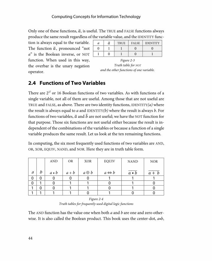
In computing, the six most frequently used functions of two variables are AND, OR, XOR, EQUIV, NAND, and NOR. Here they are in truth table form.
a
b
AND
a • b
OR
a + b
XOR
a ⊕ b
EQUIV
a ⇔ b
NAND
𝑎𝑎 • 𝑏𝑏������
NOR
𝑎𝑎 + 𝑏𝑏�������� 0 0 0 0 0 1 1 1 0 1 0 1 1 0 1 0 1 0 0 1 1 0 1 0 1 1 1 1 0 1 0 0
Figure 2-4 Truth tables for frequently used digital logic functions
The AND function has the value one when both a and b are one and zero other-wise. It is also called the Boolean product. This book uses the center-dot, a•b,
a 𝑎𝑎� TRUE FALSE IDENTITY 0 1 1 0 0 1 0 1 0 1
Figure 2-3 Truth table for NOT
and the other functions of one variable.

Digital Logic
45
to indicate AND. It is sometimes written as a ∧ b or as implicit multiplication: ab.
The OR function results in a one when either a or b, or both, are one. It is called the Boolean sum and is written a + b or sometimes a ∨ b and pronounced “or.” It is important to remember that the + symbol when used in a Boolean expres-sion is not the arithmetic plus.
The XOR function is exclusive or. It results in a one when either a or b, but not both, is one. The “not both” part is what makes it exclusive. It is written a ⊕ b. It is also called the not-equal function; when there are two variables, it is one when a ≠ b. In the case of two, and also three or more variables, exclusive or produces a one when the number of one-variables is odd, and so XOR can also be called the odd function.
The equivalence function, EQUIV, is one when a and b are equal. It is sometimes called the XNOR function because its characteristic number, 1001, is the inverse of that for XOR in the same way that OR is the inverse of NOR.
NAND is a contraction of “not and.” It is the inverse of the AND function, that is, 𝑎𝑎 • 𝑏𝑏������. From the truth table, you can see that the characteristic number for AND is 0001 and that for NAND is 1110.
NOR is a contraction of “not or” and is the Boolean inverse of the OR function, that is, 𝑎𝑎 + 𝑏𝑏��������. Check the two columns of the truth table.
Both NAND and NOR have the important property that they are functionally complete. Functional completeness is discussed in Section 2.7.
Each of the functions described above can be extended in an intuitive way to apply to three or more variables.
For completeness, the remaining four functions are a ⇒ b, 𝑎𝑎 ⇒ 𝑏𝑏��������, b ⇒ a, and 𝑏𝑏 ⇒ 𝑎𝑎��������. Recall that ⇒ is the implication symbol, so a ⇒ b is read a implies b. These functions are used infrequently if at all in digital logic.
That covers all 16 possible functions of two variables.

Computing Concepts for Information Technology
46
2.5 Boolean Algebra, Switches, and Claude Shannon’s Master’s Thesis
Claude Shannon (1916 – 2001), a mathematician and electrical engineer, made many contributions to the science of computing. One of the most important was his 1937 MIT master’s thesis, in which he showed that switching circuits could solve any problem that switching algebra could solve. In other words, we can build a switching circuit that can compute any switching algebra function. Since we can represent such functions as truth tables, we can build a switching circuit that can compute the function values given in the truth table. 28
2.5.1 Electric Circuits, Switches, and Transistors
In electrical engineering, a circuit is an arrangement that provides for a complete path from a power source like a battery, through a load like a lamp, and back to the power source. The connection back to the power source is often called “ground” by electrical engineers. Switches can be used to open the circuit, which removes power from the load.
In the circuit of Figure 2-5, the power source is a battery and the load is a lamp. Power can flow to light the lamp only if both switches are closed. Such a circuit forms the AND function. Power can flow only when switch A AND switch B are closed.
Shannon worked with electromechanical relays, where a relatively low powered electrical signal could switch circuits of much higher power. Such a relay is an electrically controlled switch. Because these devices had a mechanical compo-nent, switching speeds were on the order of tens of milliseconds. Computers like the IBM Automatic Sequence Controlled Calculator, also called the Har-vard Mark I and first used in 1944, used electromechanical relays to perform computations.
28 We will not go further into that here, but for reading on your own, a web search on “sum of products”
will show how it is done.
Figure 2-5
Electric circuit forming the AND function

Digital Logic
47
Vacuum tubes can also work as controlled switches, and can operate at elec-tronic speeds, more than 1,000 times faster than relays. The first electronic computers, like ENIAC 29, used vacuum tubes as their switching elements. Vac-uum tubes are bulky, fragile because of their glass enclosures, and have a limited lifetime because they have a heating element that operates at around a thousand degrees Fahrenheit. As the number of tubes in a computer increases, the fre-quency of failures caused by tubes “burning out” increases. That puts an upper limit on the number of tubes that could be used in a computer, and so a limit on the computational power of tube-based computers. Even so, a number of interesting and important vacuum tube computers were built in the 1940s and 1950s.
One of the most historically important machines of the vacuum tube era was EDVAC, Electronic Discrete Variable Automatic Computer. The principal im-portance of EDVAC was John von Neumann’s First Draft of a Report on the EDVAC in June, 1945. In that document, von Neumann described a binary, sequential, stored program computer. That design has come to be called the von Neumann architecture, and is the basis for design of modern computers.
The invention of the transistor at Bell Laboratories by John Bardeen, Walter Brattain, and William Shockley in 1947 allowed designers of computing ma-chines to replace vacuum tubes with transistors. Transistors were small, rugged, consumed little power, generated comparatively little heat, and could act as controlled switches just like vacuum tubes. The transistor was possibly the most important invention of the 20th century.
Almost simultaneous inventions by Robert Noyce, Jack Kilby, and Kurt Le-hovec in 1958 led to the development of the integrated circuit, which com-bined multiple transistors and other electronic components on a single piece, or chip, of silicon. Transistors in modern computer chips have switching speeds of nanoseconds or faster, more than a million times faster than relays. The earliest commercial chips had dozens of transistors; modern CPU chips have up to tens of billions of transistors. The inventions of the transistor and
29 Electronic Numerical Integrator and Computer, the first programmable general purpose electronic com-
puter, built during the World War II era and used from 1945 to 1955.

Computing Concepts for Information Technology
48
integrated circuit effectively removed power consumption and heat dissipation as limitations to the number of devices in a computing machine for most of the rest of the 20th century. 30 The remaining limit was that of size. The size of ob-jects on a chip is limited by the wavelength of the light used to project the image, or mask, onto the chip. Modern integrated circuit fabrication uses frequencies far higher than visible light. There is also a physical limit to how small a tran-sistor can be made before quantum effects overwhelm classical semiconductor physics. That limit is likely to be reached in the third decade of the 21st century. See the discussion of Moore’s Law in Chapter 0.
2.5.2 Digital Logic Gates
You saw in the previous section that the AND function can be computed using switches. Transistors can function as switches, so we could draw circuit dia-grams with a bunch of transistors showing how each of the Boolean functions of two inputs could be computed. Doing that belongs in a course in electronic engineering. Instead, we will abstract away the internal details of how such functions are computed, and also abstract away the details of power supply and return. We will use a set of stylized symbols to represent digital logic gates, electronic devices that can compute Boolean functions. The commonly-used
30 As the density of transistors in integrated circuits increased according to Moore’s law, heat dissipation
again became a limiting factor late in the 20th century.
Figure 2-6 Symbols and truth tables for important digital logic gates

Digital Logic
49
symbols and their truth tables are shown in Figure 2-6. 31 The truth tables are identical to those in Figure 2-3 and Figure 2-4.
To save space, the inputs and outputs are not labeled in Figure 2-6. We will refer to the inputs as a and b, and the output as either f or with the appropriate Bool-ean expression.
The first symbol in Figure 2-6 is the NOT gate symbol; the result is the inverse of the input. For this symbol and all the others in the table, the input is on the left and the output is on the right. As a function of one variable, its truth table has two rows. They are the same as the a and 𝑎𝑎� columns in Figure 2-3. The symbol is a triangle with a circle at the output end. The triangle is the symbol for an amplifier. The ability of one gate to drive the inputs of several others, the fan-out, is an important property when designing digital logic circuits. The cir-cle is called a negation bubble, and indicates that the output signal is inverted.
The AND symbol is a bullet shape. It computes the Boolean product. Its truth table is that of the AND column in Figure 2-4. Note that we refer to the Boolean product using the center-dot: a•b. In addition to computing the Boolean product, the AND gate can serve to perform an en-able function. Note that if ena is zero, the output of AND is always zero regardless of the value of in. However, if ena is one, the output of AND is equal to in; the AND gate has served to enable the value of in at its output when ena is one and to produce a zero otherwise.
The OR symbol is the shield shape, and computes the Boolean sum: a + b. As mentioned above, the plus symbol is pronounced “or.” It is not the same as the arithmetic plus. Its truth table is that of the OR column in Figure 2-4.
31 These are the distinctive shape symbols. Another way of drawing digital logic gates is to use the same
rectangular symbol for every type of gate and to label each rectangle with the appropriate function. The distinctive shape standard is based on a U.S. Air Force standard, formalized by American Institute of Electrical Engineers and American Society of Mechanical Engineers in 1960. When the distinctive shape symbols are used, the output is always on the “pointy end.”
ena in out 0 0 0 0 1 0 1 0 0 1 1 1
Figure 2-7 AND as enable

Computing Concepts for Information Technology
50
The XOR symbol, exclusive or, is an OR symbol with a curved chevron across the inputs. Unlike the OR gate, XOR is not one when both a and b are one; the output is one when a, exclusively, is one and when b, exclusively, is one. The XOR function is sometimes called the “odd func-tion” because it produces a one at the output when the num-ber of ones at the input is odd. Similarly, it can be considered a “not equal” function since it produces a one when the in-puts are not equal.
The XOR gate can be used as a controlled inverter as shown in Figure 2-8. Note that when inv is zero, the output of XOR is the same as in. When inv is one, the output is 𝚤𝚤𝚤𝚤� .
The EQUIV or XNOR symbol is an XOR gate with a negation bubble at the output. Its result, its characteristic number, is the inverse of XOR. The principal use of EQUIV is as a comparator; it produces a one when a and b are equal, a zero oth-erwise.
All digital logic gates require connections for power and return or ground. Those connections are abstracted away in logic diagrams, but are present in the physical circuits.
2.6 Digital Logic Building Blocks: Combinational Circuits
Digital logic gates become much more interesting when we do things with them. There are a few digital logic building blocks that occur frequently in the construction of computing equipment. We’ll look at two of them, adders and decoders, in detail, and mention some others.
inv in out 0 0 0 0 1 1 1 0 1 1 1 0
Figure 2-8 XOR as controlled
inverter
Digital Logic
51
2.6.1 Adders
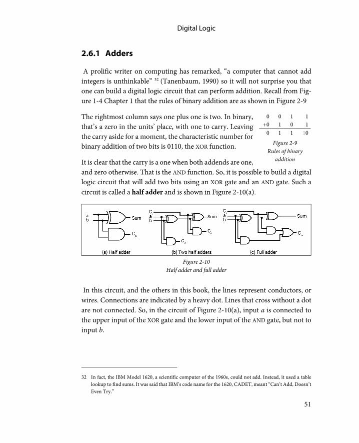
A prolific writer on computing has remarked, “a computer that cannot add integers is unthinkable” 32 (Tanenbaum, 1990) so it will not surprise you that one can build a digital logic circuit that can perform addition. Recall from Fig-ure 1-4 Chapter 1 that the rules of binary addition are as shown in Figure 2-9
The rightmost column says one plus one is two. In binary, that’s a zero in the units’ place, with one to carry. Leaving the carry aside for a moment, the characteristic number for binary addition of two bits is 0110, the XOR function.
It is clear that the carry is a one when both addends are one, and zero otherwise. That is the AND function. So, it is possible to build a digital logic circuit that will add two bits using an XOR gate and an AND gate. Such a circuit is called a half adder and is shown in Figure 2-10(a).
In this circuit, and the others in this book, the lines represent conductors, or wires. Connections are indicated by a heavy dot. Lines that cross without a dot are not connected. So, in the circuit of Figure 2-10(a), input a is connected to the upper input of the XOR gate and the lower input of the AND gate, but not to input b.
32 In fact, the IBM Model 1620, a scientific computer of the 1960s, could not add. Instead, it used a table
lookup to find sums. It was said that IBM’s code name for the 1620, CADET, meant “Can’t Add, Doesn’t Even Try.”
0 0 1 1 +0 1 0 1
0 1 1 10
Figure 2-9 Rules of binary
addition
Figure 2-10
Half adder and full adder

Computing Concepts for Information Technology
52
The half adder has a drawback: it can produce a carry out, but it has no provi-sion for a carry in. Without a carry in, one cannot add numbers larger than two single-digit binary numbers, a serious limitation.
We can use a second half adder to compute the sum of the first result and a carry in, giving a total sum of three bits. That is shown in Figure 2-10(b). The AND gate of the leftmost half adder has been moved down a bit to keep wires from crossing, but the logic is the same. We’ve solved the problem of having a carry in, but now there are two carry outs. They cannot both be one. The carry out from the first half adder is one only if a and b are both one. In that case, the intermediate sum will be zero and so the second carry out will be zero. If carry in and either a or b, but not both, is one, then the intermediate sum will be one and the carry out from the second half-adder will be one. So, if the carry out from either half adder is one, the carry out of the total sum will be one. We can connect the two carry outs with an OR gate to compute the carry out of the re-sult. That circuit is called a full adder and is shown in Figure 2-10(c).
A full adder adds two bits and a carry in to produce a one-bit sum and a carry out. We can use multiple full adders to add binary numbers more than one bit wide. Given a design for a full adder, we can abstract away the details and just draw a box labeled “full adder.” Figure 2-11 shows an adder capable of adding two four-bit binary integers.
The carry-in input of the low order (rightmost) full adder is permanently wired to logic zero. The carry-out of the low order adder is connected to the carry-in of the next one, and so on. We could make an adder capable of adding integers larger than four bits by adding more full adders on the left.
Figure 2-11 Four bit ripple carry adder

Digital Logic
53
2.6.2 Combinational Circuits and Gate Delay
The adder circuits developed above, and the other circuits discussed in this sec-tion, are combinational circuits. The output of a combinational circuit de-pends only on its input at the time; if the input changes, the output will change accordingly. In other words, combinational circuits have no memory of previ-ous states.
Modern transistors can change state from on to off or vice versa very fast; some transistors used in integrated circuits have switching speeds measured in pico-seconds. 33 However, there is always some delay between the time the input to a gate changes and the time the output reflects the changed input. The time required for the output of a gate to change state after the input has changed state is the propagation time or gate delay. It also takes time for a signal to move from one device to another. Designers of computing equipment must take this delay into consideration.
Consider the adder in Figure 2-11. If the total delay through one full adder is two nanoseconds, then the carry out from adder zero will not be correct until two nanoseconds after the inputs are applied to the adder. That means that the carry-in to the next full adder, numbered one, will not be correct until two na-noseconds after the inputs are applied. The carry in to adder two will not be correct for another two nanoseconds, and so on. The carry value “ripples” from the low order digit to the higher order digits, with each successive carry taking the time for a full adder to complete its computation. That is why the circuit of Figure 2-11 is called a ripple carry adder.
For a four-bit ripple carry adder made of full adders with two nanosecond add time, the result will not be correct until eight nanoseconds after the inputs have been applied. A 32-bit adder built in this way will take 64 nanoseconds to pro-duce correct output. To improve speed, we need more sophisticated circuits, faster transistors, or both. The adder circuit in a modern computer is much more sophisticated than our ripple carry adder and much faster. It is also much
33 A picosecond is one trillionth of a second, or 1/1000 of a nanosecond.

Computing Concepts for Information Technology
54
more expensive in terms of number of gates and chip area occupied. One of the basic trade-offs in computing is speed vs. cost.
2.6.3 Decoders, Multiplexors, and other Building Blocks
Suppose we have a signal with which we want to activate one of two outputs, perhaps a green LED when the signal is on, or as-serted, and a red one when it is off. We can do that with a single NOT gate. In the circuit of Fig-ure 2-12, if the input at a is on, the input will drive the green LED and turn it on. The output of the inverter will be a zero, or off, and the red LED will be off. Conversely, if a is zero or off, the green LED will be off, but the inverter will pro-duce a one, and the red LED will be on.
It is possible to extend this idea to an arbitrary number of inputs. Such a circuit is called a decoder. It receives a binary number at its inputs and ac-tivates exactly one of 2n outputs, where n is the number of bits of the input. In the circuit of Figure 2-12, there’s a one-bit number at a and one of two possible outputs is activated.
In Figure 2-13, there are two inputs. The high-order digit is at a and the low-order is b. If the input is 01, as shown, output 1 will be high and the others will be low. The AND gate at position one will produce an output 1
when 𝑎𝑎� and b are one. Other values at the input will select exactly one of the four possible outputs.
Figure 2-12 A one-bit decoder controls two
outputs with one signal.
Figure 2-13
A two-to-four decoder

Digital Logic
55
A complementary circuit to the decoder is an encoder. It has 2n inputs and gen-erates a n-bit binary number at its output, depending on which input is high. (Only one input is allowed to be high at any time.)
Another digital logic building block is the multiplexor, which picks one of 2n signals to transmit. It has n selector inputs, 2n data inputs, and one data output. One of the data inputs is connected to the data output. Which one? It is deter-mined by the binary number supplied at the selector inputs. The complemen-tary circuit is the demultiplexor. It has one data input, n selector inputs, and 2n data outputs. The value on the data input line is directed to one of the 2n data outputs depending on the value of the selector inputs.
2.6.4 Shifters
A shifter is a combinational circuit that can shift the bits of a word one or more places to the right or left. Shifters are used for both logical operations on data and for arithmetic.
To see how a shifter can be used for arithmetic, consider that we can multiply a decimal number by ten by adding a zero on the right, like this: 13 × 10 = 130. What has actually happened is that the original digits are shifted left one place so that the one is shifted from the tens place to the hundreds place and the three is shifted from the units place to the tens place. The added zero occupies the units place. Removing a digit on the right of a decimal number has the effect of dividing by ten; the digit removed is the remainder.
Shifting binary numbers left one place multiplies by two. Shifting right divides by two. The bit shifted out is the remainder.
When shifting numbers with pencil and paper, it is not necessary to consider what happens at the left end of a number, but computers represent numbers in fixed sizes. Adding a digit at the right means discarding a digit at the left. If a significant digit is shifted out on the left, the result is no longer multiplication by two. Some shifter circuits preserve the digit shifted out so that it can be tested for significance.

Computing Concepts for Information Technology
56
When shifting right, we must supply a digit on the left. When shifting unsigned or positive numbers, supplying a zero on the left produces the expected result. Such a shift is called a logical right shift.
A problem arises when right-shifting signed numbers because the leftmost bit represents the sign. When shifting signed numbers, we want to replicate the sign bit, supplying a zero for positive numbers and a one for negative numbers. Such a shift is called an arithmetic right shift. When shifting left, there is no distinction between logical and arithmetic shifts.
It is not uncommon for shifters to have a control signal for “no shift” that passes the input value through the shifter unchanged. Allowing the shifter to be pre-sent even when shifting isn’t needed simplifies some kinds of circuits.
Modern computer designs depend in large part on relatively few digital logic building blocks like these in the same way that modern buildings depend on a few standard sizes for things like lumber, bricks, and doors. The existence of these building blocks helps explain why it is easier to build complex hardware that works reliably than to build software of equal complexity that works equally reliably.
2.7 NAND and NOR: Circuit Equivalence and Functional Completeness
There is frequently more than one way to design a digital logic circuit. Two circuits which produce the same result for all combinations of inputs are equiv-alent.
There is an important property of NAND and NOR: each, by itself, is functionally complete. The property of functional completeness means that any Boolean ex-pression can be rewritten so that it can be computed using only NAND or only NOR operations in correct arrangement. It follows that one can design circuits using only NAND or only NOR that are equivalent to circuits using any other gates.

Digital Logic
57
Figure 2-14(a) shows that both NAND and NOR can compute the NOT function, or Boolean inverse. If signal a is connected to both inputs of a NAND gate, then both inputs will be identical, either zero or one, depending on the value of a. From Figure 2-4 we see that if both inputs to a NAND gate are zero, the result is a one, and if both inputs are one, the result is zero. The NAND gate of Figure 2-14(a) computes the NOT function.
Also from Figure 2-4 we see that if both inputs to a NOR gate are zero, the result is a one, and if both inputs are one, the result is zero. The NOR gate of Figure 2-14(a) also computes the NOT function.
Showing equivalence using Boolean algebra
Figure 2-14(b) shows the computation of AND using only NAND and only using NOR. Recall that the characteristic number of NAND is 1110, and that is com-puted by the leftmost NAND gate. The second NAND gate is wired as an inverter, and so transforms 1110 to 0001, the characteristic number of AND. The upper circuit of Figure 2-14(b) computes the AND function using only NAND gates.
The lower diagram of Figure 2-14(b) shows computation of AND using only NOR gates. We can show that circuit is equivalent to AND using Boolean algebra.
Figure 2-14
Circuit equivalence and functional completeness (a) NAND and NOR as inverters (b) Computation of the AND function
(c) Computation of the OR function.

Computing Concepts for Information Technology
58
The first two NOR gates function as inverters to compute 𝑎𝑎� and 𝑏𝑏�. The right-most NOR gate computes 𝑎𝑎� + 𝑏𝑏��������. By De Morgan’s theorem, 34 that is 𝑎𝑎� • 𝑏𝑏�; the double negations cancel, leaving a • b.
Showing equivalence using truth tables
Figure 2-14(c) shows computation of the OR function, first with NOR gates, then with NAND gates. The circuit in the up-per part of the diagram is similar to the corresponding cir-cuit of Figure 2-14(b). The leftmost NOR gate computes the NOR of the inputs, a characteristic number of 1000. The sec-ond gate inverts that, giving 0111, the characteristic number of the OR function.
We showed that the second circuit in Figure 2-14(b) was equivalent to the AND function using Boolean algebra. It is also possible to show that two circuits are equivalent using truth tables, and we will show using a truth table that the lower circuit of Figure 2-14(c) computes the OR function. The left column of Figure 2-15 enumerates all possible values of the two inputs, a and b.
The leftmost NAND gates of the lower circuit of Figure 2-14(c) function as in-verters. The middle column of Figure 2-15 shows the inverse values as com-puted by those NAND gates. The middle column is no longer in ascending binary order.
The two values in the center column are inputs to the rightmost NAND gate in the lower circuit of Figure 2-14(c). Using the truth table for NAND, we see that an input of 1 1 produces an output of 0; an input of 1 0 produces an output of 1, and so on. Column f, the result of the circuit, has the value 0111, which is the
34 De Morgan’s theorem is one of the fundamental theorems of Boolean algebra. It has both an AND form
and an OR form. The AND form is 𝑎𝑎 • 𝑏𝑏������≡ 𝑎𝑎� + 𝑏𝑏�. The OR form, used above, is 𝑎𝑎 + 𝑏𝑏�������≡ 𝑎𝑎� • 𝑏𝑏�. You may find DeMorgan’s theorem useful in developing programming logic to sort out the effect of combining AND, OR, and NOT, as well as in analyzing digital logic. The mnemonic to help you remember it is, “Break the line, change the sign.”
a b 𝑎𝑎� 𝑏𝑏� f 00 11 0 01 10 1 10 01 1 11 00 1
Figure 2-15 Computation of NOR using NAND
gates.

Digital Logic
59
characteristic number of the OR gate. We have shown that the lower circuit of Figure 2-14(c) computes the OR function.
Equivalence of more complex circuits can be shown using Boolean algebra or, for small numbers of inputs, with truth tables.
There are other combinations of gates that, together, are functionally complete. For example, the set {AND, OR} is functionally complete. NAND and NOR are important because they are the only two that are, alone, functionally complete. NAND gates are particularly important in chip design because they have better propagation performance and take up less silicon area than NOR gates. Recall the space / computational power / cost trade-offs discussed in Chapter 0.
2.8 Sequential Circuits and Memory
So far, we have considered combinational circuits. If the input to a combina-tional circuit changes, the output changes correspondingly. Combinational cir-cuits have no memory of past inputs or states. There are several ways to implement circuits with memory. One way is to use digital logic gates, but ar-range them differently. In the circuits we have considered so far, signals flow from input to output. Circuits with memory can be achieved by connecting the output of a circuit back to its input, a mechanism called feedback. Circuits that employ feedback to achieve memory are called sequential circuits.
2.8.1 The S-R Latch
The circuit of Figure 2-16 is one of the simplest memory circuits, the S-R latch. Applying a one to input S turns Q on and 𝑄𝑄� off. They will remain in that state even when S returns to zero. Applying a one to R turns Q off and 𝑄𝑄� on. The S-R latch remembers, or latches, which of S or R was seen last, even after the input is removed. We can think of S and R as set and reset, respectively. A circuit like this one that has two stable states is called bistable. The condition of S=R=1 is not al-lowed; the behavior of the circuit is unpredictable in that condition.
Figure 2-16 S-R Latch.

Computing Concepts for Information Technology
60
Because the S-R latch has memory, it cannot be described with a truth table. Instead, one needs a state table, which has Q, the output, on both the input and output sides. We will not consider state tables here, but if you’d like to make one for the S-R latch, you will need columns for S, R, and Q on the input side of the table and NextQ, often written as Q′, on the output side. Since there are three inputs, the table will have 23 = eight rows. You will not need a column for 𝑄𝑄� because it is always the inverse of Q.
2.8.2 The Clocked D-latch
The S-R latch will store one bit of data, but it’s not as convenient as we might like because we need separate signals for storing zero and one. What is really needed is one data input bit, which we call D. Recall that one-bit decoder of Figure 2-12. The one-bit decoder can generate the S signal when D is a one and the R signal when D is a zero. That is accomplished with a single NOT gate.
In addition to a single input, we need a way to control when the input is stored. The ripple-carry adder of Figure 2-11 takes eight nanoseconds after the inputs are applied to produce a correct sum. Because combinational circuits compute continuously, the output bits are always present, but they’re not correct until after the longest propagation delay, in this case eight nanoseconds, have passed. The clocked D-latch provides a way to signal when the result should be stored.
The right side of Figure 2-17 is an S-R latch. Ignoring the two AND gates for a moment, if the input at D is zero, a one will be sent to the R input of the S-R latch and a zero to the S input. If the input at D is one, a zero will be sent to R and a one to S.
Figure 2-17
A clocked D-latch

Digital Logic
61
Now we consider those AND gates. An AND gate can be used to control whether the input is passed to the output or the output is zero regardless of the input, as shown in Figure 2-7. Notice that when ena is zero, the output is always zero. When ena is one, the output is the value of in. When used this way, the AND gate performs an enable function; that is, the input is enabled to propagate to the output.
That is the function of the AND gates. The value of D is stored in Q only when the ena signal is high or true. The enable signal is often called a clock signal.
The clocked D-latch and similar circuits are level-triggered memories. The in-put, at D in the diagram, is stored any time the enable signal is true. Level-trig-gered devices are also transparent when the enable signal is high. If the value at D changes when the enable signal is true, the value at the output, Q, will also change.
2.8.3 Edge-Triggered Devices
If we think about computing systems rather than individual circuits, it is easy to see that the output of one step of a calculation is frequently the input to the next step of the calculation. That means a connection from the output back to the input. It is possible that the changed output will influence the input. Such a condition is called a hazard, and can result in erroneous results.
To overcome these problems designers use edge-triggered memory devices. In an edge-triggered device, it is the transition of the enable signal that causes the input value to be stored. Edge-triggered devices can be built to capture the value to be stored on either the rising edge of a pulse or the falling edge, or both.
2.9 Clocks and Synchronous Circuits
The diagram at Figure 2-18 shows how edge-triggered memory devices use a clock signal to store the results of a computational circuit, often a CPU, without causing hazards.
The clock cycle begins at the start of one peak and ends at the same point on the following peak. The time taken by one cycle is called the period of the clock.

Computing Concepts for Information Technology
62
The number of clock cycles per second 35 is the clock speed of a computer. The clock speed is the inverse of the period. A clock with a speed of one gigahertz completes one billion clock cycles each second, so each cycle is one nanosecond, the inverse of one billion.
The clock in Figure 2-18 is asymmetric; the time during which the clock signal is high is less than the time when the clock signal is low. The transitions from high to low and low to high are sloped in the diagram, showing that the transi-tions are not instantaneous.
In our hypothetical computer, data are sent from storage to the computing ele-ment on a low signal from the clock. Control signals describing the computa-tion are generated at the same time.
Computation takes place using combinational logic conceptually similar to the ripple carry adder of Figure 2-11, but more complex. The time required to com-plete the computation is the time for the data signals to propagate through the computational unit. In the four bit ripple carry adder, if each full adder takes two nanoseconds, the data at the outputs will not be correct until eight nano-seconds after the inputs are stable. Designers of computers know that it will take some time to set up the input signals and that all gates are not identical; some may be slightly slower than others. So, the clock period for the ripple carry 35 Strictly speaking, the correct unit of measurement for clock speed is Hertz (Hz), which is the inverse of
the period.
Figure 2-18 One clock cycle, showing edge-triggered data storage
Adapted from Tanenbaum (1999)

Digital Logic
63
adder would need to be slightly longer than eight nanoseconds. How much longer can be calculated if the characteristics of the circuits are known.
It is likely that the result of a computation will be stored in the same memory that supplied the input. However, edge-triggered memory devices will store the data far faster than the time for a signal to propagate through the computational unit, so the fact that the input changes does not cause an incorrect result.
2.10 Registers Figure 2-19 is a clocked latch that can send its output to two destinations. The input to the latch is connected to an in-put bus, which may also connect to other storage devices. There will always be one bit of data at the input to the latch, but it may not always be valid. The triangle at the clock input indicates that the latch is edge triggered on the rising edge of the signal. A negation bubble at the input would indicate that the latch is triggered on the falling edge. The AND gate that drives the clock input of the latch receives two signals, CLOCK and WRITE. The CLOCK signal is the system clock; it produces a regular train of pulses, similar to Figure 2-18. The WRITE signal is generated by a control unit. This latch will store one bit of data, whatever is on the input bus, on the rising edge of the system clock pulse, but only if the WRITE signal is also asserted.
The latch has a single output line that is always on, and is the bit that was most recently stored. The two triangular symbols on the right side of the latch are tristate buffers. A tristate buffer provides a mechanism to pass a signal or no output at all. In the on state, the input, either zero or one, is copied to the out-put; in the off state, it is as though there were no connection at all. Electrical engineers call this a high impedance state. If the ENA A signal is asserted, that tristate buffer passes the latch output to the A bus. Similar, ENA B passes the output to the B bus. Both buses can be driven at the same time, but if there are multiple latches on a bus, only one can be enabled at any given moment.
Figure 2-19
Clocked latch with two output paths

Computing Concepts for Information Technology
64
A register is a small, fast unit of storage within the central processing unit or other device. Figure 2-20 is the symbol for a regis-ter. Conceptually, a register is some number of latches, from one to 64 or more. Registers are described by the number of bits stored, so a register with 64 latches would be a 64-bit register. The number of outputs may be one, two, or possibly more than two. There is one WRITE input, and one ENABLE in-put for each output. They are connected internally to every latch in the register so that all latches store data at the same time and all latches enable their outputs at the same time. A register that holds only a few bits is sometimes called a latch, even though it may hold more than one bit.
2.11 Summary of Learning Objectives
This section of the chapter tells you the things you should know about, but not what you should know about them. To test your knowledge, discuss the following concepts and topics with a study partner or in writing, ideally from memory.
Boolean algebra is an algebra over finite sets of discrete values. It was developed in the 19th century by George Boole. The logical operators of the Boolean alge-bra important to computing are NOT, AND, OR, XOR, EQUIV, NAND, and NOR. The NAND and NOR operators are each functionally complete. Others, including C. S. Peirce and Jan Łukasiewicz, used truth tables to represent two-valued Boolean expressions. In the 20th century, Claude Shannon developed the switching algebra, a Boolean algebra in which functions and variables have only two states. Shannon showed that switching devices could compute any function that could be represented by a truth table. Switching elements are on or off. In proper arrangement, they can compute functions such as NOT, AND, OR, XOR, EQUIV, NAND, and NOR. Such devices are called digital logic gates, or just gates.
Switching devices of the early to mid 20th century were mechanical relays or vacuum tubes. Mechanical relays are slow; vacuum tubes were faster, but fragile
Figure 2-20 A register

Digital Logic
65
and with a limited life. The invention of the transistor and then the integrated circuit increased both the speed and the operating lifetime of digital logic gates.
Multiple digital logic gates can be arranged to compute much more complex functions, including arithmetic operations like addition. A relatively few types of circuits are the building blocks of modern computers. Circuits that perform computation but do not have memory are called combinational circuits.
The time required for a switching device to change states is non-zero, so the time for the output of a gate to reflect a change in the input is non-zero. This time is called the gate delay. The time for an electric signal to propagate from one device to another is also non-zero. The time for a combinational circuit’s output to reflect a change in the input is the sum of the gate delays and propa-gation delays of the longest path through the circuit, and is called the propaga-tion delay.
Because digital logic circuits take non-zero time to complete each computation, we need a mechanism to indicate when computations are complete. A clock is a circuit that generates a regular train of pulses, the period of which is long enough for the longest computation.
Digital logic circuits incorporating feedback from output to input can be used for storage of data. The simplest of these is the S-R latch, which can store one bit of data. The clocked D-latch extends the S-R latch by providing a single data input and a mechanism to enable the storage element to be loaded from the data input. The clocked D-latch is a level-triggered device. If the value of the data input changes while the clock signal is asserted, an incorrect value can be stored. Instead, edge-triggered storage devices can be used. Sampling and stor-ing the input takes place on the transition of the clock input, and not based on its level.
A clocked latch with one or more outputs can send its output to one or more buses. A register is conceptually one or more latches, up to 64 or more bits wide. If two or more registers are connected to the same bus, only one may be enabled at any given time.

Computing Concepts for Information Technology
66
2.12 References
Tanenbaum, Andrew S. (1990) Structured Computer Organization Third Edi-tion. Prentice-Hall.
Tanenbaum, Andrew S. (1999) Structured Computer Organization Fourth Edi-tion. Prentice-Hall.