2015 design automation conference p - chipdesign...
TRANSCRIPT
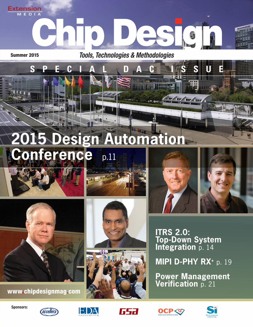
2015 Design Automation Conference p.11
ITRS 2.0: Top-Down System Integration p. 14
MIPI D-PHY RX+ p. 19
Power Management Verification p. 21
www.chipdesignmag.com
Sponsors:
S P E C I A L D A C I S S U E
Summer 2015


JULY 14 –16MOSCONE CENTERSAN FRANCISCO
SEMICON West is brought to you by

EDITOR'S NOTE
The International Technology
Roadmap for Semiconductor
(ITRS) has changed. It is no longer
primarily focused on manufacturing
challenges that need to be overcome
to enjoy the benefits of continued
scaling. Instead, ITRS 2.0 as it’s called,
is starting with a system level approach
and working down to the chip and transistor level. “ITRS
2.0 is alive and well,” says Paolo Gargini, longtime ITRS
chairman.
This new approach is described in detail in this month’s story
on pg. 15 “ITRS 2.0: Top-Down System Integration.” System
Integration prescribes ways of assembling heterogeneous
building blocks into coherent systems.
“The world has changed so much that if we didn’t look at
system requirements and then project that down onto devices,
we were going to be out of sync,” Gargini said. “We spent last
year essentially doing this.”
Interestingly, Gargini said the semiconductor industry has
evolved to the point today where it is similar to what he
experienced in the 1970s when he was working at Fairchild..
“The design was 100% in the hands of the system companies.
It was very difficult to handle the business because typically
they would not reveal what was right or wrong.” One such
project was how Polaroid handled the development of a new
chip for its SX70 camera. Fairchild and TI got the assignment
By the end of the ‘70s, Gargini moved to Intel. “We got
lucky in that IBM selected Intel and Microsoft. They thought
it was going to be a very small business. They just wanted to
make sure they could cover everything from the large super
computer to the miniscule PC,” Gargini said.
By the end of the 80s and throughout the 90s that technology
had become so efficient that there was a switch from a three
year cycle to a “real” two year cycle. “In reality, for processors,
it was a three or four year schedule. The real change was to
make this two year cycle real,” Gargini said. “In essence, Intel
and Microsoft dominated the business and what was left for
the PC company was to assemble the memory, screen and
other elements. The business really got turned around.”
Another big change came around 2007, with the first iphones
and mobile devices. “The main difference was that instead of
buying a processor, a dynamic RAM, a static RAM, a video
chip, the interface and so forth, the system designer could
take just a little bit of everything and put it on a single die or
maybe two dies at the most that would completely satisfy the
system that they were building,” Gargini said. “Like in the
70s, the system designer had absolute control over what the
die was supposed to do.”
By the second introduction in 2010 of the tablet, this really
new business model began taking traction. “It was clear that
the world had changed. By 2012, I outlined to the ITRS
groups that we were going to change,” Gargini said.
As a first step, the ITRS groups looked at all of today’s
applications and dissected them into their basic building
blocks. “First of all, we needed system integration that would
look at all these different applications and identify what the
basic building blocks were,” Gargini said. “We looked at
iphone and tablets and the reverse engineering analysis and
the different chips. Out of this we said ‘okay’ we understand
the overall system integration. The main element is that you
have system-on-chip and in addition you can stack different
chips. You’re really in the world of heterogenous integration.”
ITRS 2.0 still has a focus on More Moore. “One category is to
push CMOS to the limits and see what it can do. Many of the
systems can be built on this existing roadmap for CMOS. We
can see still going forward into the next decade,” Gargini said.
On the other hand, the effort that began in 2005/2006 —
called ‘beyond CMOS’ — produced a lot of devices. “They’re
not perfect yet, but we can understand enough. Which of
these devices could augment the way you do this integration?
Finally, we said once we got all these elements, how would
the factory look once you put all these elements together.” ◆

September 9-10-11, 2015Rio, Las Vegas
www.InterDrone.com
A BZ Media Event
Meet with 80+ exhibitors!Demos! Panels! Keynotes!
The Zipline!
For Builders More than 35 classes, tutorials and panels for hardware and embedded engineers, designers andsoftware developers building commercial drones and thesoftware that controls them.
For Flyers and BuyersMore than 35 tutorials andclasses on drone operations, flying tips and tricks, range, navigation, payloads, stability,avoiding crashes, power, environmental considerations,which drone is for you, and more!
For Business Owners, Entrepreneurs & Dealers
Classes will focus on running a dronebusiness, the latest FAA requirementsand restrictions, supporting and educating drone buyers, marketingdrone services, and where the nexthot opportunities are likely to be!
InterDrone is Three Awesome Conferences:
Pete [email protected]
Gabe Moretti
Shannon Davis
Chris Ciufo, Anne Fisher
Caroline Hayes, Cheryl Ajluni, Dave Bursky, Brian Fuller, David Lammers, Craig Szydlowski, Ed Korczynski, Jeff Dorsch
Thomas L. Anderson, Vice President of Marketing, Breker Verification Systems, Inc.
Senior Director, Corporate Programs and Initiatives, Synopsys Lisa
Hebert, PR Manager, Agilent
Spryte Heithecker
Stephanie Bradbury
Mariam Moattari
Jenna JohnsonSales Director
Michael ClowardSales Manager
Jenna Johnson [email protected]
www.chipdesignmag.com/subscribe
Chip Design is sent free to design engineers and engineering managers in the U.S. and Canada developing advanced semiconductor designs. Price for
LLC. All rights reserved. Printed in the U.S.
The year’s DAC will be held June 7-11 at the Moscone Center in San Francisco.
By Pete Singer, Editor-in-Chief
2
By Pete Singer, Editor-in-Chief
6
By Dr. Bruce McGaughy, Chief Technology Officer and Senior Vice President of Engineering, ProPlus Design Solutions, Inc.
By Lauro Rizzatti, Verification Consultant
By Andrew B. Kahng, Professor of CSE and
ECE, University of California, San Diego,
Juan-Antonio Carballo, Senior Manager,
Embedded Solutions, AMD, and Paolo
Gargini, Chairman, ITRS
+
By Ashraf Takla, Mixel, Inc., and Thomas Rodriguez, Freescale Semiconductors, Inc.
By Vijay Chobisa, Mentor Graphics
Corporation
By Gabe Moretti, Senior Editor
By Brian Fuller, Cadence Design Systems
24
Cover images courtesy of the Moscone Center
and the Design Automation Conference
ESDi - ESD Protection Network
Integrity Analysis
Mixel ’s MIPI D-PHY RX+ ;
Mixel ’s MIPI M-PHY
Model 5220
27

Is your company a missing piece in the EDA & IP industry? The EDA Consortium Market Statistics Service (MSS) is the timeliest and most detailed market data available on EDA & IP. Top companies have been participating in the MSS since 1996, but no report is complete without ALL the pieces.
If your company is not contributing to the MSS, it is a missing piece in the puzzle. Contribute your company’s data to the MSS and receive a complimentary Annual MSS Executive Summary.
What’s in it for your company? Worldwide statistics on EDA & IP revenue Ability to size your market Six years of market data for trends analysis The opportunity to make a positive difference
in the industry
For details contact:[email protected](408) 287-3322www.edac.org
Receive a Complimentary EDA & IP Industry Market Report

IN THE NEWS
Margaret R. Martonosi, Hugh
Trumbull Adams ’35 Professor of
Computer Science at Princeton
University, has been selected as
the Marie R. Pistilli Women in
Electronic Design Automation
(EDA) Achievement Award
recipient for 2015. The award honors
Dr. Martonosi for her technical leadership of high-impact research
projects in the design of power-efficient computer architectures and
sensor systems as well as her creation and organization of career
development programs for women and minorities. As a highly
visible woman in leadership positions at Princeton and within her
professional community, Martonosi also has acted as a mentor and
role model for graduate and undergraduate women students.
Martonosi is a Fellow of both IEEE and ACM. She was the 2013
recipient of the Anita Borg Institute Technical Leadership Award.
She also has received the 2013 NCWIT Undergraduate Research
Mentoring Award and the 2010 Princeton University Graduate
Mentoring Award. In addition to many archival publications,
Martonosi is an inventor on seven granted US patents, and has
co-authored a technical reference book on power-aware computer
architecture. She serves on the Board of Directors of the Computing
Research Association (CRA).
Mentor Graphics Corp. announced the new Calibre® xACT™
parasitic extraction platform that addresses a wide spectrum of
analog and digital extraction needs, including 14nm FinFET,
while minimizing guesswork and setup efforts for IC designers.
The Calibre xACT platform delivers the best combination of
accuracy and turnaround time (TAT) by automatically optimizing
its extraction techniques for the customer’s specific process node,
application, design size, and extraction objectives. Customers
using the Calibre xACT platform for parasitic extraction have
experienced improvements in turnaround time as high as 10X,
while meeting the most stringent accuracy requirements.
Samsung has worked extensively with Mentor Graphics on the
development and qualification of the Calibre xACT platform for
14nm, and used it during technology development because of the
high accuracy it provides. The Calibre xACT product’s ability to
employ a single rule deck for a range of extraction applications
allows customers to get the accuracy and fast TAT they need without
having to manually modify their rule decks or tool configuration.
Circuit designers have to wrestle with performance versus accuracy
throughout the design cycle. Parasitic extraction is no different.
With the leading process nodes using more complex FinFET
devices, design engineers are pushing for tighter accuracy, while
also needing higher performance and capacity for billion transistor
designs. In fact, all process nodes are seeing growing complexity
with the mix of memory, analog, standard cell, and custom digital
content in modern ICs. This complexity poses a range of different
challenges for extraction tools. To meet these requirements the
Calibre xACT platform uses a combination of compact model,
field solver and efficient multi-CPU scaling technologies to ensure
robust accuracy as well as turnaround performance needed to meet
schedule deadlines.
The Calibre xACT extraction platform is integrated with the entire
Calibre product line for a seamless verification flow, including the
Calibre nmLVS™ product for complete transistor-level modeling,
and the Calibre xACT 3D product for targeted, extreme-accuracy
extraction applications. It also interoperates with third-party design
environments and formats to ensure compatibility with existing
design and simulation flows.
Cadence Design Systems, Inc. announced the Cadence® Indago™
Debug Platform, a new debugging solution which reduces the
time to identify bugs in a design by up to 50 percent compared
to traditional signal- or transaction-level debug methods. In
addition to the Indago Debug Platform, Cadence also announced
three debugging apps that plug into the platform and can be used
with other verification tools to provide a single integrated and
synchronized debug solution for testbench, verification IP (VIP),
and hardware/software debug for system-on-chip (SoC) designs.
With its patented root-cause analysis technology, the Indago
Debug Platform filters unneeded data to go beyond the source for
a single bug to resolve the cause of all related bugs. Current debug
methodologies used by designers require multiple simulation
iterations to incrementally extract data points that ultimately
point to the source of the bug. The technology in the Indago
Debug Platform can reduce the human time necessary to resolve
schedule-impacting bugs by up to 50 percent using a common set
of resources that enable a suite of commercial and user-created
IN THE NEWS
Apps that automate the analysis of data from multiple verification
engines and multiple vendors.
With a unified debug platform and the debug apps, the Indago
Debug Platform enables multiple engineering specialists from
design, testbench, embedded software and protocol verification to
operate as a team to resolve SoC bugs. The three debug apps are:
Indago Debug Analyzer: Extends root-cause analysis from
e testbench (IEEE 1647) to SystemVerilog (IEEE 1800)
and increases performance by up to 10X
Indago Embedded Software Debug: Resolves bugs
associated with embedded software applications by
synchronizing software and hardware source code debug
Indago Protocol Debug: Visualizes advanced protocols
such as DDR4, ARM® AMBA® AXI and ACE using
Cadence VIP for intuitive debugging
Mentor Graphics Corporation announced the Nucleus real time
operating system (RTOS) targeting high-performance, next-
generation applications for wearable embedded devices designed for
medical, fitness, security, safety and other sectors. The introduction
of new multicore system-on-chip (SoC) architectures targeting
wearable devices with Internet of Things (IoT) features requires
an operating system that has a framework tailored to meet new
system requirements. The Nucleus RTOS framework for smart
wearable devices connects to other smart devices, gateways, or
directly to the cloud. Optimized for size, performance, and power
efficiency in unicore or multicore SoCs, the Nucleus RTOS is the
first embedded operating system to provide a power management
and processor lifecycle framework to maximize wearable device
battery life.
The Nucleus RTOS provides memory space partitioning in both
high-performance microprocessor units (MPU) and resource-
constrained microcontroller units (MCU) to support software
updates and upgrades in deployed systems. The Nucleus RTOS
includes a rich IPv4/v6 networking stack, M2M protocols, and
security for IoT applications and cloud connectivity.
Cadence Design Systems, Inc. announced that its USB 3.0 host
IP solution for TSMC’s 16nm FinFET Plus (16FF+) process is
one of the first to pass USB-IF compliance testing and receive
USB-IF certification. The complete controller and PHY integrated
solution is pre-verified, which enables designers to mitigate project
risk and reduce system-on-chip (SoC) integration and verification
time. Cadence offers a complete USB 3.0 solution including the
controller, PHY and verification IP. The certified USB 3.0 host
solution for 16FF+ features an innovative architecture developed
by FinFET design experts within Cadence and offers a 40
percent reduction in dynamic power consumption versus previous
generations of the IP on other process nodes. To achieve this power
reduction, the integrated USB host xHCI controller and PHY IP
utilize power and clock gating in order to conserve energy as the
USB protocol goes into a low-power sub-state. Additionally, the
PHY is optimized to ease integration. With a reduced pinout, there
are fewer combinations to verify and less complexity with fewer
complex software interactions that need to be tested and debugged.
Synopsys, Inc. announces the availability of Verification IP (VIP)
for the DDR4 3D Stacking (3DS) specification. Synopsys VIP for
DDR4 3DS, based on its native SystemVerilog UVM architecture,
is architected for ease of integration and configurability. The VIP
for DDR4 3DS supports all JEDEC commands and provides
pre-built DIMM (UDIMM, RDIMM, LRDIMM) models
with protocol and timing checks, including support for memory
vendor and the JEDEC standard part configurations. Synopsys'
VIP for DDR4 3DS is natively integrated with its Verdi® Protocol
Analyzer, offering a graphical protocol-aware debug environment
that synchronizes memory transactions with signals. Complete
with verification plans and built-in coverage, Synopsys' VIP for
DDR4 3DS accelerates verification closure for designers of next-
generation memory interfaces that require higher capacity and
performance and reduced power to support enterprise computing
devices, servers and data centers.
TSMC and Mentor Graphics reached the first milestone of their
collaboration on 10nm EDA certification. Calibre® physical
verification and design for manufacturing (DFM) platform, and
the Analog FastSPICE™ (AFS™) Circuit Verification Platform,
including AFS Mega, are certified by TSMC based on the most
current version of 10nm design rules and SPICE models. New
tool feature enhancement based on 10nm process requirements
has been made in Olympus-SoC™ digital design platform with
TSMC validation, and certification of full chip integration is
actively on-going. In addition to 10nm, Mentor has also completed
16FF+ version 1.0 certification of the Calibre, Olympus-SoC and

IN THE NEWS
AFS platforms. These certifications provide designers with the
earliest access to signoff technology optimized for TSMC’s most
advanced process nodes, with improved performance and accuracy.
The Analog FastSPICE Platform provides fast circuit verification
for nanometer analog, RF, mixed-signal, memory, and custom
digital circuits. For large circuits the AFS Platform also delivers
high capacity and fast mixed-signal simulation. For embedded
SRAM and other array-based circuits, AFS Mega delivers highly
accurate simulation results.
As circuit reliability remains a focus, Mentor and TSMC have
enhanced the Calibre PERC™ product offering in 10nm to ensure
that design and IP development teams have robust verification
solutions for identifying sources of electrical error. Additionally,
the Calibre xACT™ extraction suite includes updated models to
deliver more accurate results to fulfill tighter accuracy requirements
of 10nm.
For TSMC’s 16FF+ 1.0 Calibre design kit release, the Calibre team
has worked with TSMC to speed up DRC performance by 30% on
average. In addition, TSMC and Mentor released new filling use
models that will improve first-pass fill runs, making ECO changes
easier and faster. The new fill methodology will also help ensure
consistent cycle times during post fill verification.
Synopsys, Inc. expanded its IP Accelerated initiative with support
for ARM® processors with the new DesignWare® Hybrid IP
Prototyping Kits. The kits enable designers to prototype the ARM
processor and memory elements of a design in a virtual environment
for superior debug visibility, and to develop software for the
DesignWare interface IP in an FPGA-based environment for
high-performance execution with real-world interface connectivity.
The Hybrid IP Prototyping Kits accelerate IP development by
combining a Synopsys Virtualizer™ Development Kit (VDK)
with a DesignWare IP Prototyping Kit consisting of a HAPS®-
DX FPGA-based prototyping system with a DesignWare IP
reference design. The VDK includes a virtual prototype of the
ARMv8 Base Platform containing an ARM Cortex®-A57 plus
Cortex-A53 big.LITTLE™ system. The Hybrid IP Prototyping
Kits accelerate prototyping, hardware and software integration and
system validation, enabling designers to start software development
months earlier in the design cycle.
STATS ChipPAC Ltd. announced that Cavendish Kinetics, a
provider of high performance RF MEMS tuning solutions for LTE
smartphones and wearable devices, has adopted its advanced wafer
level packaging technology to deliver Cavendish’s SmarTune™ RF
MEMS tuners in the smallest possible form factor, as a 2mm2 chip
scale package.
LTE smartphone original equipment manufacturers (OEMs) are
rapidly adopting antenna tuning solutions to be able to provide the
required signal strength across the large number of LTE spectrum
bands used globally. Cavendish’s SmarTune RF MEMS tuners
outperform traditional RF silicon-on-insulator (SOI) switch-based
antenna tuning solutions by 2-3dB, resulting in much higher data
rates (up to 2x) and improved battery life (up to 40%). Cavendish
RF MEMS tuner shipments are ramping aggressively and can now
be found in six different smartphone models across China, Europe
and North America, with many additional designs in development.
Synopsys, Inc. announced the availability of a broad portfolio of
DesignWare® PHY IP for TSMC’s 16-nanometer (nm) FinFET
Plus (16FF+) processes. The silicon success of the DesignWare IP
in TSMC’s 16FF+GL and 16FF+LL processes enables designers
to accelerate the development of SoCs that incorporate embedded
memories and interface IP for USB 3.0, 2.0 and HSIC; PCI
Express® 4.0, 3.0 and 2.0; SATA 6G; HDMI 2.0; MIPI D-PHY;
DDR4/3 and LPDDR4/3/2 protocols on TSMC 16FF+ processes.
The DesignWare STAR Memory System® product is a
comprehensive, integrated test, repair and diagnostics solution that
supports Synopsys and third-party embedded memories. TSMC
uses DesignWare STAR Memory System to characterize all of its
16FF+ memory compilers. The optimized test and repair algorithms
maximize test coverage while reducing test time, lowering test
cost and improving manufacturing yield. Synopsys also provides
DesignWare Logic Libraries for the TSMC 16FF+ processes that
include 7.5-, 9- and 10.5-track libraries, power optimization kits
and High Performance Core (HPC) kits. All Synopsys embedded
memories and logic libraries, including those on TSMC 16FF+
processes, work seamlessly with the IC Compiler™ II place-and-
route system that accelerates throughput and improves quality of
results.
IN THE NEWS
Keysight Technologies, Inc. introduced the Advanced Design
System PCI Express and USB Compliance Test Benches, which
enable a complete workflow for SerDes engineers, from simulation
of a candidate design, through measurement of the finished
prototype. The solution is designed for semiconductor companies
developing SerDes I/O blocks and OEMs integrating such chips
onto their system PCBs.
Both compliance test benches are available as add-ons to the
Advanced Design System 2015.01 Channel Simulator software
from Keysight EEsof EDA. Engineers using the new test benches
can now use simulation to ensure a candidate design yields a
fabricated prototype compliant to the specifications of the PCI
Special Interest Group (PCI-SIG®) and USB Implementers
Forum (USB-IF), respectively. Previous tools for this task made
it difficult to correlate simulation compliance with hardware
prototype and test bench compliance.
The ADS PCI Express and USB Compliance Test Benches
rectify this situation by providing a customizable test harness in
which to simulate customers’ intellectual property. The test bench
also provides a post-processing scripting capability, known as
Waveform Bridge, which exports simulated waveforms to the same
compliance application used with Keysight Infiniium oscilloscopes.
The new version of the Infiniium software works on live real-time
data from an oscilloscope and on stored data from an oscilloscope or
from ADS (offline mode). In addition, the software works not only
on the PC embedded in the oscilloscope, but also on an ordinary
standalone Windows PC (offline/remote mode). Using this new
offline/remote mode, engineers can run the compliance application
side-by-side on the same PC hardware on which they run ADS.
ANSYS, Inc. announced today that its ANSYS® RedHawk™ and
ANSYS Totem™ products are certified by TSMC for the most
current version of 10nm FinFET Design Rule Manual (DRM)
and SPICE models, addressing the power and performance
requirements for mobile, computing and networking applications.
TSMC has certified these solutions for static and dynamic voltage
drop analysis and advanced signal and power electromigration
(EM) verification to meet the 10-nanometer requirements.
Complex device structure and high drive currents in FinFET
devices make power integrity and EM key design requirements.
With innovative algorithms and analysis engines, ANSYS solutions
deliver needed accuracy while reducing turnaround time to meet
the increased computational requirements caused by modern
products’ growing design complexity. Advanced technology
support in RedHawk and Totem, including EM rule compliance
and color-aware resistance extraction, help deliver greater reliability
and manufacturability.
Mentor Graphics Corp. announced its new Xpedition® Package
Integrator flow, the industry’s broadest solution for integrated
circuit (IC), package, and printed circuit board (PCB) co-design and
optimization. The Package Integrator solution automates planning,
assembly and optimization of today’s complex multi-die packages.
It incorporates a unique virtual die model concept for true IC-
to-package co-optimization. In support of early marketing-level
studies for a proposed new device, users can now plan, assemble
and optimize complex systems with minimal source data. The new
Package Integrator flow allows design teams to realize faster and
more efficient physical path finding and seamless tool integration
for rapid prototyping, right to the production flow.
This solution ensures that ICs, packages and PCBs are optimized
with each other to reduce package substrate and PCB costs
by efficient layer reduction, optimized interconnect paths, and
streamlined/automated control of the design process. The Xpedition
Package Integrator product also provides the industry’s first formal
flow for ball grid array (BGA) ball-map planning and optimization
based on an “intelligent pin” concept, defined by user rules. In
addition, a groundbreaking multi-mode connectivity management
system (incorporating hardware description language (HDL),
spreadsheet and graphical schematic) provides cross-domain pin-
mapping and system level cross-domain logical verification.
DAC2015
The biggest change at this year’s Design Automation
Conference (DAC), to be held June 7-11 at the
Moscone Center in San Francisco, is that everyone will
be able to attend the keynote talks and Skytalks. In past
years, the exhibit floor opened at the same time as the
general sessions and keynotes, and attending the Skytalks
require a full conference pass. This year, says Anne Cirkel,
General Chair for the 52nd DAC, the exhibits will open
later, at 10:00, to avoid a conflict with the keynotes which
start at 9:00. “We want everybody to see the keynotes and
everybody to be able to attend the Skytalks,” Cirkel said.
The Skytalks, which are shorter 20 minute keynote type
talks, will be in the DAC pavilion on the show floor at
1:00 and 3:30 pm each day (Booth 311). That’s during a
scheduled break with the general conference, so there is
no conflict. The Skytalks were launched for the first time
at the 50th DAC in Austin in 2013.
Cirkel said some other changes include additional content
for designers, with submissions to the designer track up
30%. There will also be a big focus on security, automotive
and embedded.
In the Wednesday keynote, for example, Jeff Massimilla,
Chief Product Cybersecurity Officer at GM will be joined
on-stage by Craig Smith, founder of OpenGarages.
org and author of the 2014 Car Hacker’s Manual. The
discussion will be moderated by John McElroy, host of
Autoline Daily and a Detroit auto news Icon. The title of
the joint talk: “Cyber Threats to Connected Cars: Staying
Safe Requires More Than Following the Rules of the
Road.”
The automotive initiative at DAC, which was started
last year, will have a single track for three days. “For the
first time, we are going to have Tesla speak,” Cirkel said.
“You’re also going to see names like GM, Ford, Delphi,
Chrysler, Infineon and Bosch.”
There will also be a big focus in the Internet of Things
(IoT) at DAC. The goal is to bring together the electronic
design ecosystem in order to highlight the key challenges
hindering IoT and to assess the range of solutions available
to create a sustainable future for IoT.
Cirkel said that embedded technology is also an important
part of DAC. “Not only because Embedded Techcon is
co-located this year, but our own content in embedded is
growing,” she said. “We will see an even larger increase in
embedded developers coming to the show.”
In addition to Embedded Techcon, co-located events
include:
ACM/IEEE System Level Interconnect Prediction
(SLIP)
CELUG/EDAC Enterprise Licensing Conference
IBM Annual HPC Seminar and LSF Technical
Workshop
Electronic System Level Synthesis Conference
(ESLsyn)
IWLS - International Workshop on Logic and
Synthesis
THE SCHEDULEDAC begins on Sunday, June 7th, with a full day of
workshops, concluding with a welcome reception from
5:30-7:00pm at the Intercontinental Hotel, Grand
Ballroom BC.
The nine Sunday workshops run from 9:00 am to 4:30 pm:
Low-Power Image Recognition Challenge
(LPIRC)
Design Automation for Beyond-CMOS
Technologies
SEAK 2015: DAC Workshop on Suite of
Embedded Applications and Kernels
System-to-Silicon Performance Modeling and
Analysis

DAC
2015
Computing in Heterogeneous, Autonomous 'N'
Goal-Oriented Environments
Design Automation for HPC, Clouds, and Server-
Class SoCs
Requirements Driven Verification (for Standards
Compliance)
Enterprise-Level IP Management for the DAC
Semiconductor Professional
Interdisciplinary Academia Industry Collaboration
Models and Partnerships
The exhibits will be open until 7:00pm on Monday-
Wednesday, with a cocktail reception from 6:00-7:00 pm
on Monday and Tuesday. See the DAC conference site
for a listing of the 168 exhibitors and an interactive show
floor map. http://www.dac.com/. Exhibiting companies
are primarily focused on:
Electronic Design Automation (EDA)
Intellectual Property (IP)
Embedded Systems and Software
Automotive Systems and Software
Design Services
Security
The Technical Program, which runs Monday-Thursday
includes panels, special sessions, a designer track, an IP
Track and an automotive track.
KEYNOTE AND VISIONARY TALKSMONDAY, JUNE 8
Dr. Brian Otis, Google
Google Smart Lens: IC Design and
Beyond
We have amazingly sparse access to
information about our own bodies. Indeed,
the healthier we are, the less data we collect. Technologies
to continually monitor critical biomarkers are still in
their infancy, but continuing advances in chip design and
biocompatible system integration will help define the next
generation of these devices. Against the backdrop of the
Google Smart Contact Lens platform, I’ll share thoughts
on the scarcity of power, extreme miniaturization, and
end-to-end connected systems that span the design
space from transistors to the cloud. Along the way, I’ll
cover chip design techniques for body-worn systems and
wireless sensors and present examples of constantly-
connected devices for improving healthcare. These areas
present tough unsolved problems at the interface between
the IC and the outside world that cannot be solved by
transistor technology scaling alone. The interface between
silicon and the human body is highly variable, erratic, and
messy. This unpredictability impacts sensor performance,
RF/electromagnetic performance, system reliability,
tolerability and comfort, etc. Several future applications
will demand thin-film realization and biocompatibility
of complex systems. Novel power sources, low power IC
design techniques, microscale user interface technologies,
and new system integration techniques will be a few of
the enabling technologies for these emerging systems.
TUESDAY, JUNE 9
Vivek Singh, Intel
Moore’s Law at Fifty: No End in Sight
Moore’s Law is an observation that a
transistor – the fundamental building
block of the digital age – will decrease in
cost at a steady, exponential rate. This decrease in cost as
well as transistor size over the past 50 years has also led to
dramatic increases in compute power and energy efficiency
and transformed our world with ever-more powerful smart
phones, tablets, personal computers and data centers.
It has also enabled computing to become a powerful yet
invisible force in our homes, offices, cars, factories and
much more. These imperatives are the reason Moore’s Law
will continue, and motivated teams will continue to find
innovative solutions to the engineering challenges of the
day, just as they have in the past. This talk will provide some
examples of how complex problems have been overcome
in recent technology nodes, including those from the field
of Computational Lithography. Inverse Lithography and
Source Mask Optimization are two such examples that have
helped extend the life of 193 patterning. Such innovations,
fed by a rich technology pipeline, give us confidence that
Moore’s Law will continue.
Jeffrey Owens, CTO of Delphi
The Design of Innovation that Drives
Tomorrow
When people think of high tech devices,
they rarely think of their cars, trucks or
vans. Similar to the computational power of the human
brain, today’s vehicles possess more processing power than

DAC2015
anything most consumers own or will purchase. A typical
car is equipped with more than 50 computers designed to
operate at automotive grade capabilities for an extended
period of time.
Vehicle manufacturers and automotive suppliers around
the world are responding to a myriad of consumer
preferences and regulatory initiatives -- including
enhanced safety features, increased fuel economy, reduced
emissions and connectivity.
Vehicles of the future will require increased amounts of
embedded software and electrical/electronic systems.
Addressing this dynamic will require significant design
automation aids to handle extreme complexity. Electronics
and design automation will play a critical role in shaping
the future of automotive by providing design technology
that helps save lives, protect the environment and provide
a satisfying in-car experience for drivers and passengers
alike.
WEDNESDAY, JUNE 10
Jeff Massimilla, Chief Product
Cybersecurity Officer at GM
Craig Smith, founder of
OpenGarages.org and
author of the 2014 Car
Hacker’s Manual
John McElroy, host of
Autoline Daily and a
Detroit auto news Icon
Cyber Threats to Connected Cars: Staying
Safe Requires More Than Following the
Rules of the Road
Cars increasingly are networked computing platforms
and with this burgeoning connectivity comes more
vulnerability to possible cyber-attacks. We expect our
vehicles to continue to evolve and support internet
capabilities via WiFi and cellular data networks, connect
to our mobile computing platforms via Bluetooth, provide
GPS navigation assistance, and automatically link to the
manufacturer to help with diagnostics. However, all those
connectivity features create entry point for hackers. Can
we make our cars more secure? Or should we accept the
fact that they are as vulnerable as our computers at home?
Come hear from the real experts on stage. John McElroy,
Producer of Autoline Detroit will guide you through
an in-depth chat between Jeffrey Massimilla, Chief of
Cybersecurity at GM, and Craig Smith, author of the Car
Hacker Manual.
THURSDAY, JUNE 11
Dr. John Rogers, University of Illinois
Electronics for the Human Body
Biology is soft, curvilinear and adaptable;
silicon technology is rigid, planar and
immutable. Electronic systems that
eliminate this profound mismatch in properties create
opportunities for devices that can intimately integrate
with the body, for diagnostic, therapeutic or surgical
function with important, unique capabilities in biomedical
research and clinical healthcare. Over the last decade
a convergence of new concepts in materials science,
mechanical engineering, manufacturing techniques and
device designs has led to the emergence of diverse classes
of ‘biocompatible’ electronics. This talk describes the key
ideas, with examples ranging from ‘cellular-scale’ light
emitting diodes that can be injected into the brain for
optogenetic behavioral control to bioresorbable electronics
that can serve as non-antibiotic bacteriocides for treating
surgical site infections.
SYS
TEM
IN
TEGR
ATIO
NIT
RS 2
.0
The mission of the System Integration (SI) focus team
in ITRS2.0 is to establish a top-down, system-driven
roadmapping framework for key market drivers of the
semiconductor industry drivers in the 2015-2030 period.
The SI focus team is currently developing and constructing
roadmaps of relevant system metrics for Mobility, Internet of
Things (IoT) and Big Data drivers. Mobility, embodied by the
smartphone product, has redefined the existing ITRS SOC-
CP (consumer portable system-on-chip) driver with richer
feature requirements. IoT, as one of the fastest-growing market
segments of electronic devices, imposes significantly different
design considerations from conventional electronics design
due to low-power and ubiquitous deployment requirements.
As a fast-growing aspect of the datacenter, microservers have
been separated out from the conventional server market
segment. For these new drivers, the SI focus team seeks to new
indicators (e.g., energy efficiency) as functionalities expand,
architectures evolve, and heterogeneous integration soars.
CHANGES IN THE SEMICONDUCTOR INDUSTRY SUPPLY CHAINThe 1980s and 1990s saw a semiconductor industry dominated
by integrated device manufacturers (IDMs). During this
period, the architecture of the main driver in the ITRS, the
microprocessor unit (MPU), was not application-driven.
Standard components in PC and server systems, e.g., memories
and microprocessors, scaled their densities and operating
frequencies continuously to meet aggressive performance
and cost requirements. Applications had to be designed
based on these components. However, in the past ten years,
fabless design houses have changed the industry landscape.
Design teams have been building customized system-on-chip
(SoC) and system-in-package (SIP) products, rather than
building standard components, to address specific application
requirements. As applications evolve, they drive further
requirements for heterogeneous integration, outside system
connectivity, etc. A key goal of the SI focus team is to extract
the technology requirements hidden behind the evolution of
end products such as smartphones and microservers. The IoT
is recognized as another driving market and application for the
semiconductor industry; system metrics and semiconductor
technology requirements pertaining to IoT are still in the
preliminary stages of roadmapping.
MOTIVATIONS AND DISTINCTIONS OF SYSTEM DRIVERSHistorically, the ITRS has used metrics such as transistor
density, number of cores, power, etc., to roadmap technology
evolution of ICs. These metrics are essentially driven by the
physical-dimension scaling as predicted by Moore’s Law.
However, new requirements from applications such as mobility,
datacenters, etc. require a new, system-level roadmapping
approach, as these applications imply roadmaps for system-
level metrics (e.g., the number of sensors, memory bandwidth,
etc.). The ITRS roadmapping process as previously seen in
the System Drivers Chapter has not explicitly incorporated
these system-level product requirements. Therefore, a crucial
goal of “ITRS 2.0” is to connect emerging system product
drivers, along with corresponding metrics, into the ITRS’s
semiconductor roadmapping methodology.
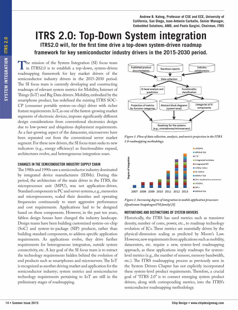
Figure 1. Flow of data collection, analysis, and metric projection in the ITRS
2.0 roadmapping methodology.
Figure 2. Increasing degree of integration in mobile application processors
(Qualcomm SnapdragonTM family) [1].

The Global Semiconductor Alliance (GSA) mission is to accelerate the growth
and increase the return on invested capital of the global semiconductor industry
by fostering a more effective ecosystem through collaboration, integration and
innovation. It addresses the challenges within the supply chain including IP,
EDA/design, wafer manufacturing, test and packaging to enable industry-wide
solutions. Providing a platform for meaningful global collaboration, the Alliance
identifies and articulates market opportunities, encourages and supports
entrepreneurship, and provides members with comprehensive and unique
market intelligence. Members include companies throughout the supply chain
representing 25 countries across the globe.
GSA Member Benefits Include:
Access to Profile Directories
Ecosystem Portals
IP ROI Calculator
IP Ecosystem Tool Suite
Global Semiconductor Funding, IPO and M&A Update
Global Semiconductor Financial Tracker
End Markets Tool
MS/RF PDK Checklist
AMS/RF Process Checklist
MS/RF SPICE Model Checklist
Collaborative Innovation Study with the Wharton School
Discounts on various reports and publications including:
Wafer Fabrication & Back-End Pricing Reports
Understanding Fabless IC Technology Book
IC Foundry Almanac, 2011 Edition
Global Exposure Opportunities:
Advertising
Sponsorships
Member Press Section on GSA Web site
Company Index Listing on Ecosystem Portals
Member Spotlight on GSA Web site
12400 Coit Road, Suite 650 | Dallas, TX 75251 | 888-322-5195 | T 972-866-7579 | F 972-239-2292 | www.gsaglobal.org

SYS
TEM
IN
TEGR
ATIO
NIT
RS 2
.0
INITIAL DRIVER ROADMAPPING METHODOLOGY USED BY SYSTEM INTEGRATIONThe roadmap process in ITRS2.0 is
summarized in Figure 1. (i) Calibration
data comes from sources such as published
data from web searches, specification
documents, datasheets and whitepapers from
IC companies, teardown reports, and high-
level comments from industry collaborators.
(ii) Function categories are obtained by
clustering analysis of IC components. Based
on the categorization, we create abstract block
diagrams as system models. We also analyze the components
and project how metrics such as maximum operating
frequency, die area, number of antennas, number of sensors,
etc. evolve over the roadmap’s 15-year horizon. Finally, we
produce a roadmap for system-level metrics based on the
projected metrics and the abstract block diagrams.
SMARTPHONE DRIVERIn recent years, mobile devices, notably smartphones, have
shown significant expansion of their computing capabilities.
Since smartphone systems are built with multiple heterogeneous
ICs (e.g., logic, memory, microelectromechanical systems
(MEMS), and radio-frequency (RF)), we must understand
tradeoffs at the system level. Beyond the current ITRS SOC-
CP roadmap, ITRS 2.0 introduces a new smartphone driver
to comprehend and roadmap metrics at a higher, system level
for mobility applications. Figure 2, based on the Qualcomm
Snapdragon family of SOCs [1], illustrates the growth of
features and degree of integration in recent application
processors (APs). Each new technology generation (aka
“node”), which enables reduced computation power (e.g., new
instruction set architecture (ISA), new devices, new low-power
techniques) or the introduction of new features (e.g., graphic
processing unit (GPU) or 1080p video), brings an increased
number of vertically-stacked bars in the plot. Figure 2 shows
that the degree of integration after 2008 keeps increasing to
meet the demands of (i) higher computation performance,
(ii) faster wireless connections, and (iii) richer multimedia
capabilities. The increasing number of heterogeneous
components (RF, logic, memory and MEMS) complicates
the system design and blocks form factor reductions, while
increasing the smartphone design cost and power budget.
A system (board-level) power projection (5% growth in power
per year) is shown in Figure 3(a). A 4.5W power management
gap, relative to a system maximum power requirement of
4W, is projected to exist at the 15-year horizon. The power
management gap for board-level power leads to a number
of design challenges (heat and thermal/thermomechanical
design, battery life, etc.). We expect that extremely aggressive
low-power design techniques will need to be applied to IC
components in smartphones to address power management
challenges. Figure 3(b) shows a projection for a second output
metric, namely, board area. An area gap of up to 46cm2 (relative
to a 60cm2 limit) is seen by the end of the roadmap, suggesting
implying footprint reduction via vertical integration.
Fig. 4(a) shows the scaling of the number of pixels in
smartphone displays. Display pixels of smartphones are driven
by high definition standards (e.g., 720p, 1080p, 4K, etc.).
Increase in the display size increases the memory bandwidth
requirement as shown in Figure 4(b). By 2029, ultra HD
resolutions of 7680 × 4320 could potentially increase memory
BW requirements to 148Gb/s. The rapid growth of bandwidth
demands for system level interconnects and off-device
interconnects is considered to be a challenge
for smartphone design.
KEY CHALLENGES AND PROMISING SOLUTIONSSeveral challenges exist in the development of
the smartphone driver, based on the projection
of system metrics.
The form factor challenge. As sizes of
smartphones shrink, especially their thickness,
Figure 3. Implied requirements for smartphone board area and system power.
Figure 4. Scaling of display size and memory bandwidth.

ITRS 2.0SYS
TEM IN
TEGRATION
adding new functionalities within compact form factors
becomes very challenging. Two obvious challenges for
technology development are:
components should keep shrinking even though the
memory bandwidth requirement and #components
increase; and
such as logic, memories, non-volatile memories (NVMs),
MEMs, RF/analog/mixed-signal (RF/AMS), should
keep increasing to reduce the required footprint.
The system-level power management challenge. Since the
projected board power of smartphones will be well beyond the
3-4W product limitation even by 2018, system-level power
management is a clear challenge. The roadblocks to address
this challenge are as follows.
on faster signaling and wider system buses, which will
increase the board-level power consumption.
components implies more PCB traces. Shrinking
smartphone form factors are expected to worsen this
problem since routing traces will be more complicated,
with added costs stemming from mitigation of
interference as well as power implications of inter-chip
communication.
The system-wide bandwidth challenge. System-wide
bandwidth refers to the bandwidth between application
processors and memories or application processors and other
peripherals. As the requirement of higher compute performance
and #functionalities, display bandwidth keep growing (as
indicated by the scaling of #APs, #GPUs, #sensors, #pixels,
and the communication bandwidth), delivering proportionate
system-wide bandwidth will become challenging. Another
aspect of this challenge will be the tradeoffs between power
management and bandwidth.
Communication bandwidth scaling. A further challenge is
implicit in the gaps between projections of required cellular
data rate or WiFi data rate and achievable data rates. As the
required communication standards supported by a single
RF module keep increasing, cost-feasible process and device
technologies must enable smartphones to integrate more
bands and communication standards within a fixed PCB
footprint budget.
MICROSERVER DRIVER AND METRICSIn this section, we describe the main features, key metrics,
key challenges, and potential solutions for the challenges of
microserver driver.
Recent studies of datacenters (e.g., by Doller et al. [2]) suggest
that high-performance MPU (MPU-HP) and networking
SOC (SOC-NW) products are the main components in
datacenters. These products may be implemented either in a
single chip or in a multichip module (MCM). An optimized
datacenter architecture cannot be achieved with a single chip
as its key building block; rather a, co-optimization of storage,
interconnects and software is required. Since the raw data
stored in datacenters is usually sparse, pre-processing that
is typically executed in traditional server cores is precluded,
due to energy budget. Besides integration of power-efficient
cores within an energy budget, datacenters require high
bandwidth and accessibility for local memories (mostly non-
volatile memories) to execute data-intensive operations. Due
to datacenter-specific optimizations and system-level design
requirements such as high rack density and cooling capacity,
the metrics of servers in datacenters are different from those
of server chips in existing products which are comprehended
by ITRS.
Some new design challenges to microserver driver are
introduced by their deployment in datacenters. Big data
computing requires a drastic reduction in communication
latencies to meet an under-100ms requirement, that is, data
must be increasingly localized. The collected data suggest
that the microserver driver addresses the cost issue by
limiting the number of cores per rack unit and the latency
issue by localizing user-specific search data. The volume of
information in datacenters is anticipated to grow at a very
high rate (every two years, or even faster). When users search
for specific information, latencies can be on the order of tens
of milliseconds because datacenters typically store information
in a highly distributed manner. As datacenters grow in
size, communication latencies increase along with power
consumption (e.g., 75MW). To limit power and temperature
of datacenters, companies are forced to invest huge amounts
of money to establish and maintain power plants adjacent to
datacenters, and to construct datacenters in geographies with
“natural refrigeration”. There is a limit to such investment in
power plants and cooling. Cooling costs, which can reach over
35% of electricity costs, continue to rise in server farms and

SYS
TEM
IN
TEGR
ATIO
NIT
RS 2
.0???
datacenters; this creates a need to reduce the number of cores
and operating frequencies to limit this cost.
To reduce operation cost, microservers must maximize the
number of cores in a rack unit subject to power and thermal
constraints. Form factor, energy-efficiency, and networking
throughput are important for this driver. As a consequence,
demand for reduced form factor and system design effort
drives the integration of the MPU and the chipset. Compared
to a 1U server (MPU-HP in ITRS), a microserver has a
higher degree of integration as it includes on-chip Ethernet
and peripheral hubs. Recent MPUs for microservers integrate
application-specific accelerators to improve energy efficiency.
Hence, high integration of functionalities is another potential
challenge.
KEY CHALLENGES AND PROMISING SOLUTIONSThe service latency challenge rises in microserver design
because of the crucial requirement for service latency.
Reference [3] proposes much more pessimistic metrics (from
50 percentile to 99 percentile latency) to ensure service quality
could be guaranteed when Big Data are hosted. To address
this application requirement, the solutions are expected from a
wide range of providers.
latency, the high-radix photonics switching network
is expected to be introduced to address the internode
bandwidth requirement.
will be unable to address access time requirements for
Big Data, spindle-based hard drives will be replaced by
non-volatile memories.
(e.g., for MPU to memories or memories to NVMs),
better heterogeneous integration solutions are expected.
(2) The node density/cooling/power management
challenge. To ease the cost of datacenter deployment,
the following challenges are identified by SI focus team.
To provide sufficient computing resource with MPU cores
and application-specific accelerators,
that more functionalities could be hosted in the same
die area and avoid power increase resulting in too much
overhead to the cooling equipment.
in each computing node is expected to ease the power
management challenge by reducing the power impact.
adaptive power management with on-die power sensors
[6] are expected to be developed to address the power
management issue.
The Electro-Optical Integration Challenge. Since the power
and performance requirements of datacenter are both crucial,
highly-integrated photonics inter-node network is expected
by 2020 [3]. Since the electro-optical interfaces are distributed
all over the datacenter, it is necessary to develop on-chip
photonics modulators and detectors to reduce the power,
space, and performance overhead due to off-chip converters
for electro-optical interfaces.
CONCLUSIONSITRS2.0 will, for the first time, via its system integration
(SI) focus team, drive a top-down system-driven roadmap
framework for key semiconductor industry drivers in the
2015-2030 period. The SI focus team is working to complete
a roadmap of relevant metrics for Mobility (smartphone),
Internet of Things (IoT), Big Data (microserver) drivers, and
possibly other product segments that will be critical top-down
drivers in the semiconductor industry of the next 15 years. ◆
REFERENCES[1] http://en.wikipedia.org/wiki/Qualcomm_Snapdragon
asanovic.pdf

ESLTEST
BIST
D-PHYSM RX+ is a Mixel proprietary implementation[1]
for Camera Serial Interface (CSI) and Display Serial
Interface (DSI) D-PHY Receiver optimized for small area and
low power, while achieving full-speed production testing, in-
system testing, and higher performance compared to traditional
receiver configurations.
There are multiple reasons why it is crucial to test an IC as early
as possible in its life cycle such as cost and safety concerns. The
Rule of Ten, which is widely accepted in the electronics industry,
states that the cost of discovering a defective chip increases by an
order of magnitude at each successive level of integration, from
die/package, to board and system.
In safety sensitive applications, cost and risk grow even faster,
and the implications of a failing part are intolerable. As electronic
component contents rapidly grows in those applications, the cost
of failure increases substantially, and detection of any degradation
in performance as early as possible is highly desirable. Full-speed
production testing enables detection of manufacturing faults and
helps drive down the number of defects to zero, as required in
safety sensitive applications such as in the automotive industry.
Testing of integrated circuits is done in order to achieve one of
three goals: detection, diagnosis, and device characterization.
Detection determines whether or not the device under test
has any faults. This involves identification of process flaws as
well as detection of chips that must not be sold to customers.
Diagnosis involves locating and identifying of a specific faults
that are present in the tested device. Device characterization is
the identification of errors in the actual design or in the testing
procedure.
MIPI Physical layer differs significantly from many existing
interfaces. In particular the D-PHY can and does switch in real-
time between two modes, High-speed (HS) using LVDS signals
and Low-power (LP) using single-ended CMOS logic signals.
It is difficult to test both HS and LP blocks using ATE. That is
why BIST is a valuable feature particularly for D-PHY testing.
BIST has many benefits including the ability to test the chips
across several layers of abstraction (IC, PCB, etc.), improving
controllability and observability, external test equipment is
simplified or eliminated, tests are performed at chip speed (which
is increasingly difficult using ATEs), and BIST performance
follows process technology improvements, whereas ATEs
technology lags behind.
BIST has drawbacks as well. Area overhead can lead to yield
deterioration and reliability degradation, additional hardware in
the loop causes increased delays and timing issues, and BIST
strategy must be decided early in the development cycle so it can
be implemented on-chip.
+
Figure 1. Test and repair cost vs. product phase at point of fault detection.
Figure 2. D-PHY Universal Lane configuration supports testability at the
expense of large overhead.

BIST
TEST
The D-PHY universal Lane, shown in Figure 2, has many
blocks connected to the high-speed serial interface (LPTX,
HSTX, LPRX, HSRX, LP-CD) resulting in high parasitic cap,
not only due to block input capacitance but also due to parasitic
interconnect capacitance. This puts an artificial upper limit on
data rate.
Traditional D-PHY implementation that can support at-
speed production test uses the Universal Lane configuration.
A D-PHY RX application would require inclusion of both the
HS & LP TX in each of the data lanes in addition to the clock
lane. This results in a considerable amount of overhead in RX
applications, since D-PHY HS and LP TX are significantly
larger than the corresponding RX only configuration, which is
shown in Figure 3.
The Mixel proprietary implementation of the MIPI D-PHY
compliant RX+ configuration combines the small area
and improved performance of RX configuration with the
testability and diagnostics that are possible with Universal lane
configuration, the best of both worlds. This is shown in Figure 4.
Since the D-PHY TX area is significantly larger than that of RX,
Mixel’s RX+ configuration has smaller area and standby current,
as only two transmitters are need instead of the five transmitters
that would be needed for a conventional 4 data-lanes Universal
lane configuration. The reduction in area is about 35% while
standby power reduction is about 50%.
The RX+ configuration has clear advantage in many aspects.
Mixel proprietary implementation of RX+ configuration enables
early detection and diagnosis of faults through the whole life
cycle of the product from wafer-sort all the way to in-system
testability. It also simplifies ATE requirements, and enables at-
speed testing (production and in-system), with minimal increase
in area.
To summarize, the RX+ is a Mixel innovative solution to
D-PHY’s serious testability challenges. This unique MIPI
compliant configuration results in area and power savings and
improved testability in full-speed production test and in in-
system testability and diagnostics. It combines the testability of
universal lane with the small size and improved performance of
RX only configuration.
NOTES:1. The RX+ configuration was developed and implemented by
Mixel independent of the MIPI® Alliance and is Compliant
with MIPI Alliance’s D-PHYSM RX ◆
Ashraf Takla is President and CEO of Mixel Inc., which he founded in
1998. Before founding Mixel, he was Director of Mixed-Signal Design at
Hitachi Micro Systems, and also worked at AMI and Sierra Semiconductors.
Mr. Takla has 35 years of experience in analog and mixed signal design,
and holds 5 patents. Mixel has been an active MIPI member since 2006.
Thomas Rodriguez received his Bachelor of Science in Electrical Engineering
from the University of Texas at San Antonio in 1998. Upon graduation
he began working as a Test Engineer at Motorola SPS until 2001. From
2001 to present he has been a member of the Analog IP design team of the
Automotive Microcontroller group at Freescale Semiconductors Inc. where he
has focused on PLL and high speed serial communications design activities.
Figure 3. R X only configuration is quite smaller that a Universal lane, but
cannot support full-speed production test.
Figure 4. Mixel's R X+ optimized configuration.
POWER
SoCsFor system-level power management verification, it is
important to understand how software applications
running on the targeted SoC effect power use. During system-
level verification, it is imperative to verify that the software
power control applications properly initialize power states and
power domains. In addition, that signals are stable during the
transition from one application to another or between tests and
level shifters, and that isolation cells are inserted correctly.
Companies that design complex SoCs implement several
power domains in their designs to meet power budgets while
maintaining the required operating performance. Several
low power management techniques are employed including
isolation cells, level shifters, state retention cells, power aware
memories, and power control logic. As some memories are
power aware, memory behavior must also be validated at the
system level. The power control logic resides in hardware and
the actual controls come from software, making verification
too complex and lengthy for traditional digital simulators.
An advanced emulation platform supports complete power
management verification at the system level, where software
and hardware operate together where real-world stimulus
is applied to the design under test. The speed of emulation
allows designers and verification teams to boot the operating
system and quickly stress test the design over an extremely
large number of power sequences.
POWER MANAGEMENT VERIFICATION FLOWSA power management structure allows designers to divide
designs into several power domains. Each domain can be
operated with a unique voltage level and can be powered on
and off without interfering with the functionality of other
domains. This requires isolation between power ON domains
and power OFF domains. When an OFF domain needs to
wake up, it requires some basic information to return to ON
correctly. Designers use retention techniques to preserve
this information while the domain is switched off. The more
information retained, the more real estate consumed; but the
domain wakes up faster. Designers must be aware that states
in the power OFF domain that lack a retention infrastructure
can go to unknown values. Level shifters are used to operate
domains at different voltages.
Memories can switch to three different states: power ON
(allows normal memory operations), power OFF (memory
operations are disabled and memory contents are corrupted),
and standby (memory operations are disabled but memory
contents are kept intact).
n this system, the always ON block implements the isolation
interfaces and schemes. Features of the UPF standard are
used to accomplish this functionality: an always ON supply
and an ON/OFF supply. The Veloce operating system (OS3)
supports the UPF supply functions — supply_off/supply_on
— to natively handle this behavior.
Together, the four stages described below create a scalable,
progressive flow that allows users to begin system-level low
power verification early in the design and verification flow,
using high-level models, adding detail and accuracy as the
design matures. The stage used depends on how far along the
design and its corresponding UPF description is in overall
development. Each stage has specific goals and actions that
build toward full verification of the final netlist.
STAGE 1: VERIFYING UPF ACCURACY AND IMPLEMENTATIONSemiconductor companies want to start low power verification
as early as possible to shorten production schedules. To make
this happen, it is critical that the UPF file accurately captures
the design intent as the design blocks are coming together at
an early stage (Figure 1).
At this stage, the design is in RTL, and the entire power
intent is defined using top level UPF file. Typically it is carried
over from a previous design and must be modified to suit the
new one. The RTL is still in an early stage of development.
There are no Liberty files and no gate-level components at this
stage. The testbench is also in an early stage of development.
Figure 1. UPF file accurately captures the design intent.

SoC
sPO
WER
Appropriately, verification takes place at a high level of
abstraction, where speed is more important than accuracy.
First, engineers verify that the UPF file is correct, and then
verify that the DUT and UPF file are working together—that
the syntax matches. After that has been validated, the emulator
reads the design RTL plus the UPF file, generates the power
hierarchy along with the design netlist, and maps everything
to emulation primitives. This step is used to verify the structure
from the top level point of view to make sure that the emulator
takes this UPF file and creates the proper power infrastructure
in the DUT; including power switches, connectivity, and
isolation cells. If anything is not implemented correctly or is
missing in the UPF file, it is corrected both in the UPF file
and the backend implementation.
STAGE 2: ADDING MULTIPLE BLOCKS AND CORRESPONDING BLOCK-LEVEL UPF FILESIn this stage, the design has several RTL blocks — each
having its own UPF file. As in Stage 1, there are no gate-level
netlists or Liberty files at this point.
The chip is verified with the top-level (power intent) UPF file
and the UPF files for each block, which are usually supplied
by the IP/block developers. Because each block-level UPF file
has been implemented, they are more accurate at representing
the power control inside each block. The top-level UPF file
verified in Stage 1 is used at this stage, so the block-level and
top-level UPF files are used together to thoroughly verify the
whole design (Figure 2).
The verification runs are similar to those in Stage 1. The main
difference is that the power control is more detailed and the
main goal is to make sure that the internal block controls are
working correctly in the whole chip environment. Because
each power pin control is more complicated in this context,
compared to Stage 1, a finer level of resolution is required
to control different sequences and cover all the corner cases.
It is essential to test the handshaking between these blocks
in the system context, because although these blocks and
their respective UPF files have been verified in isolation, it
is important to verify that they interact correctly with other
blocks at the system level.
Designs often have many power sequences coming from
different voltage regulators, and these can be powered on
and off at any time. Further, there is not a single source that
is controlling all of this activity. These are the real- world
behaviors, which engineers want to mimic in emulation.
The emulator generates random power sequences that can
randomly power the different blocks on and off, which mimics
the random nature of real-world scenarios.
STAGE 3: MIX OF RTL AND GATE-LEVEL NETLISTIn stage 3, some components of the design are fully ready and
are available as a gate-level netlist. For RTL blocks, power
intent comes from a UPF file, and for gate level block power
infrastructure, is part of the netlist. This requires support of a
liberty file. These gate level block or IP could be reused from
previous SoC (Figure 3).
At this point in the design cycle, the software is maturing
and the CPU is used to control power down and power up
functionality. So designers need to test this functionality in the
hardware/software context.
The emulator must be capable of reading UPF files and
liberty files to enable this mix of RTL and gate level netlist
verification. This is very critical at this stage.
As before, the accuracy of the UPF file matching the real chip
is the primary goal. Toward that end, the emulator needs to
provide power structure visual checking and the ability to
Figure 2. The chip is verified with the top-level (power intent) UPF file and the
UPF files for each block.
Figure 3. Designers test functionality in the hardware/software context.

POWER
SoCs
report any mismatches. Again, only emulation can provide
the required runtime performance to handle these complex
operations on a very large chip, especially with gate level
components.
STAGE 4: VERIFYING GATE-LEVEL NETLISTSIn this stage, the power management infrastructure is part of
the gate-level netlist and includes the final power hierarchy and
reads the power strategy from Liberty files. This enables the
final SoC netlist to be verified before chip tape out, ensuring
that the final netlist has accurate low power behavior and
avoiding translation issues from one design stage to another.
Veloce identifies the power hierarchy and provides a debug
flow in the event of incorrect or expected behavior (Figure 4).
ADVANCE LOW POWER DEBUG CONSOLE Power aware bugs can be hard to debug thus a comprehensive
GUI to debug power aware issues is needed. The Visualizer
Debug Environment from Mentor offers a comprehensive
power aware debug environments to enable debugging power
aware issues, connectivity and sequences in an intuitive way.
Some examples:
PA domains
PA crossings capturing various aspects of isolation/
level shifter being missed/incorrect
PA SimChecks
Power hierarchy schematic
CONCLUSIONCompanies start power aware verification at a very early
stage in the design flow and add details and granularities as
the design progresses. The successive refinement at each stage
allows customers to break down a complex problem into
smaller, targeted verification jobs and establish a feedback
loop to and from the backend team.
The Veloce Emulation platform from Mentor allows users
to approach power management verification at the system
level, where both software and hardware operate together
with real-world stimulus applied to the design under test.
The speed of emulation lets designers and verification teams
boot the operating system and run application stress tests on
the design through a very large number of power sequences
extremely quickly. The Veloce Emulation platform is fully
aligned with the Questa® simulator from Mentor, enabling
customers to use the same UPF files and UPF constructs for
both simulation and emulation.
The emulation team at Mentor has worked with customers
to create a system-level power management verification
methodology that achieves thorough verification of the
interactions between software and hardware and confirms that
system resources are powered appropriately in each functional
mode. This makes the Veloce Emulation Platform a logical
choice for power management verification for companies who
see advantages in using standards and avoiding non-standard
methodologies. The Veloce Emulation Platform complies
with the IEEE 1801 Unified Power Format (UPF 2.0 and
2.1) standards; including comprehensive constructs support
and debug capabilities.◆
Figure 4. Final SoC netlist is verified before chip tape out.
SoC
sPO
WER
It was not long ago that the issue of Low Power was handled
as an exception by the EDA industry. Today every electronic
circuit designers must minimize power consumption, although
the reasons for such requirement may vary. Battery life,
thermal management, energy conservation due to economic
factors, regulatory concerns like Energy Star from the U.S.
Department of Energy, remote execution environments like
space or under oceans, are some of the reasons to minimize
power consumption.
EDA vendors provide power analysis tools as well as power
aware development like synthesis, place and route tools, but it
has been shown by many academic papers that the best results
are obtained at the architectural level. At that point designers
have a better sense of what can be either shutdown or taken to
a slower state of execution.
THE POWER MANAGEMENT CHALLENGEDesigner must worry about both active power and leakage
power. Engineers address the problem from a functional point
of view by segmenting the circuit into domains dedicated to the
execution of functions that are somewhat independent from
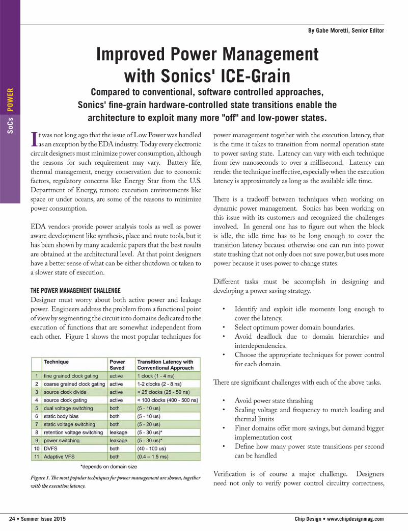
each other. Figure 1 shows the most popular techniques for
power management together with the execution latency, that
is the time it takes to transition from normal operation state
to power saving state. Latency can vary with each technique
from few nanoseconds to over a millisecond. Latency can
render the technique ineffective, especially when the execution
latency is approximately as long as the available idle time.
There is a tradeoff between techniques when working on
dynamic power management. Sonics has been working on
this issue with its customers and recognized the challenges
involved. In general one has to figure out when the block
is idle, the idle time has to be long enough to cover the
transition latency because otherwise one can run into power
state trashing that not only does not save power, but uses more
power because it uses power to change states.
Different tasks must be accomplish in designing and
developing a power saving strategy.
Identify and exploit idle moments long enough to
cover the latency.
Select optimum power domain boundaries.
Avoid deadlock due to domain hierarchies and
interdependencies.
Choose the appropriate techniques for power control
for each domain.
There are significant challenges with each of the above tasks.
Avoid power state thrashing
Scaling voltage and frequency to match loading and
thermal limits
Finer domains offer more savings, but demand bigger
implementation cost
Define how many power state transitions per second
can be handled
Verification is of course a major challenge. Designers
need not only to verify power control circuitry correctness, Figure 1. The most popular techniques for power management are shown, together
with the execution latency.
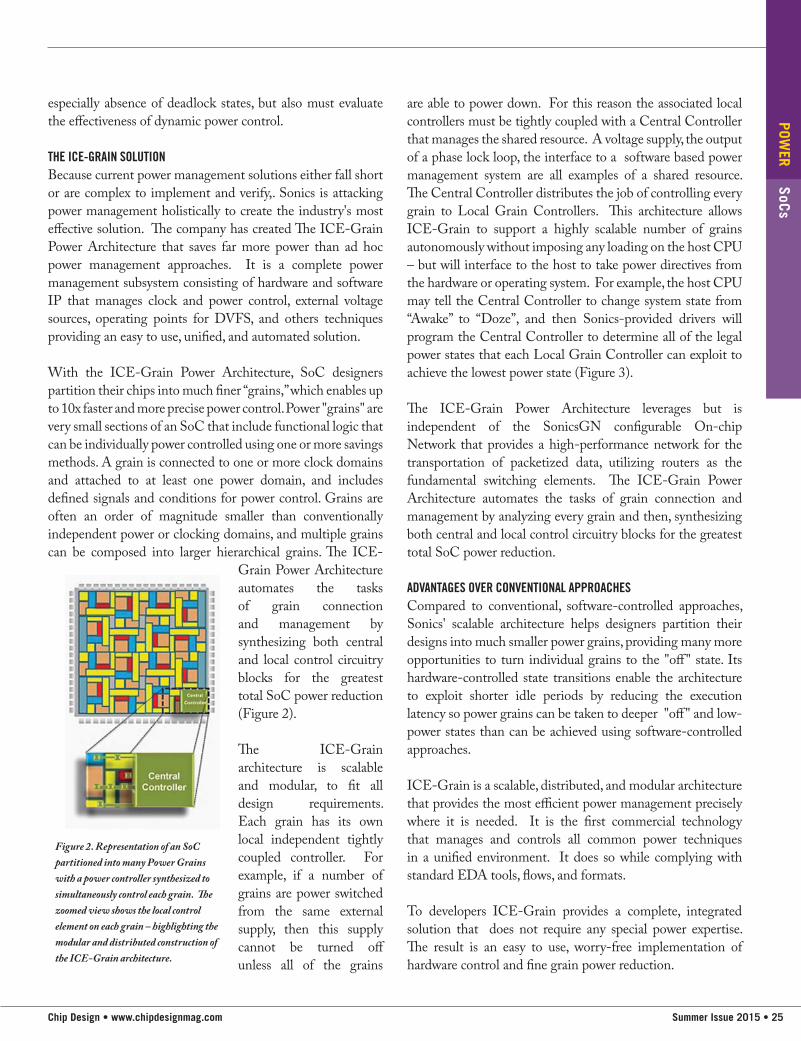
SoCs
POWER
especially absence of deadlock states, but also must evaluate
the effectiveness of dynamic power control.
THE ICE-GRAIN SOLUTIONBecause current power management solutions either fall short
or are complex to implement and verify,. Sonics is attacking
power management holistically to create the industry's most
effective solution. The company has created The ICE-Grain
Power Architecture that saves far more power than ad hoc
power management approaches. It is a complete power
management subsystem consisting of hardware and software
IP that manages clock and power control, external voltage
sources, operating points for DVFS, and others techniques
providing an easy to use, unified, and automated solution.
With the ICE-Grain Power Architecture, SoC designers
partition their chips into much finer “grains,” which enables up
to 10x faster and more precise power control. Power "grains" are
very small sections of an SoC that include functional logic that
can be individually power controlled using one or more savings
methods. A grain is connected to one or more clock domains
and attached to at least one power domain, and includes
defined signals and conditions for power control. Grains are
often an order of magnitude smaller than conventionally
independent power or clocking domains, and multiple grains
can be composed into larger hierarchical grains. The ICE-
Grain Power Architecture
automates the tasks
of grain connection
and management by
synthesizing both central
and local control circuitry
blocks for the greatest
total SoC power reduction
(Figure 2).
The ICE-Grain
architecture is scalable
and modular, to fit all
design requirements.
Each grain has its own
local independent tightly
coupled controller. For
example, if a number of
grains are power switched
from the same external
supply, then this supply
cannot be turned off
unless all of the grains
are able to power down. For this reason the associated local
controllers must be tightly coupled with a Central Controller
that manages the shared resource. A voltage supply, the output
of a phase lock loop, the interface to a software based power
management system are all examples of a shared resource.
The Central Controller distributes the job of controlling every
grain to Local Grain Controllers. This architecture allows
ICE-Grain to support a highly scalable number of grains
autonomously without imposing any loading on the host CPU
– but will interface to the host to take power directives from
the hardware or operating system. For example, the host CPU
may tell the Central Controller to change system state from
“Awake” to “Doze”, and then Sonics-provided drivers will
program the Central Controller to determine all of the legal
power states that each Local Grain Controller can exploit to
achieve the lowest power state (Figure 3).
The ICE-Grain Power Architecture leverages but is
independent of the SonicsGN configurable On-chip
Network that provides a high-performance network for the
transportation of packetized data, utilizing routers as the
fundamental switching elements. The ICE-Grain Power
Architecture automates the tasks of grain connection and
management by analyzing every grain and then, synthesizing
both central and local control circuitry blocks for the greatest
total SoC power reduction.
ADVANTAGES OVER CONVENTIONAL APPROACHESCompared to conventional, software-controlled approaches,
Sonics' scalable architecture helps designers partition their
designs into much smaller power grains, providing many more
opportunities to turn individual grains to the "off" state. Its
hardware-controlled state transitions enable the architecture
to exploit shorter idle periods by reducing the execution
latency so power grains can be taken to deeper "off" and low-
power states than can be achieved using software-controlled
approaches.
ICE-Grain is a scalable, distributed, and modular architecture
that provides the most efficient power management precisely
where it is needed. It is the first commercial technology
that manages and controls all common power techniques
in a unified environment. It does so while complying with
standard EDA tools, flows, and formats.
To developers ICE-Grain provides a complete, integrated
solution that does not require any special power expertise.
The result is an easy to use, worry-free implementation of
hardware control and fine grain power reduction.
Figure 2. Representation of an SoC
partitioned into many Power Grains
with a power controller synthesized to
simultaneously control each grain. The
zoomed view shows the local control
element on each grain – highlighting the
modular and distributed construction of
the ICE-Grain architecture.

SoC
sPO
WER
ICE-Grain saves power in three main ways: enable designers
to reliably create very fine-grained power objects, execute
power state transitions in hardware that is up to 10x faster than
software, and finally utilize a "wake on demand" technique
that detects when a grain that has been powered down needs
to wake up – and does so automatically.
Figure 4 shows a comparison between the result of a software
driven power management system and what ICE-Grain
will achieve. The dark green area represent a locality on the
SoC that can be idle for a certain length of time at a specific
execution point. Total power will be saved by taking this
hardware to a lower power state. To get to the lower power
state using a software controlled technique the host processor
needs to execute a sequence of functions. During that time
no power is saved in fact extra power is consumed by the
required processing. When the hardware that had been taken
to the lower state must resume normal execution, another
sequence of functions, again requiring additional power must
be performed. In the example shown, the CPU-based system
will consume more energy entering and exiting the low-power
state than is saved in the low-power state itself.
In contrast, the ICE-Grain switching occurs in hardware and
does not involve the host processor. So both the time it takes
to transition and the amount of power needed to effect the
transition in either direction is far less, as shown by the light
green areas representing additional power savings compared
to the CPU-based controller. In this example, expending
the energy to enter and exit the low-power state will lower
overall system power. Thus, ICE-Grain can save power
over conventional approaches in all cases and can exploit
idle regions too short for conventional approaches to save
additional power.
CONCLUSIONThe history of the electronics industry offers a number of
instances where software techniques used early to achieve
specific targets are later replaced with hardware based
technology that yields more efficient results.
Compared to conventional, software controlled approaches,
Sonics' fine-grain hardware-controlled state transitions enable
the architecture to exploit many more "off" and low-power
states. The idea of minimizing the size of the block controlled
is key because it allows designers to ignore other regions of
the larger block with logic states that would otherwise inhibit
the application of power management to the smaller hardware
region. Controlling smaller blocks like the grains in the
ICE-Grain architecture would require such large overhead in
software to make it impossible to apply. ◆
Figure 3. Architecture of Central Controller and associated Local Grain
Controllers.
Figure 4. ICE-Grain hardware-controlled state transitions are far
faster and lower-power than CPU-based power managers.
DAC2
015
Each Design Automation Conference (DAC) brings with
it its own themes, most driven by recent commercial or
academic technology developments, others driven by public
announcements. Five years ago, one of the major DAC
themes was IP and EDA firmly joined at the hip. That was
because Cadence had just acquired Denali and its memory
and interface IP portfolio.
So what will be this year’s hot themes when the 52nd DAC
convenes in the “cool, gray city of love,” San Francisco? To
understand them, let’s step back briefly. Today, electronics
design is driven by a handful of fundamental opportunities.
Among them is the increasing proliferation of semiconductor
content into existing markets (automotive and industrial
come to mind). Electronic systems design also is being driven
by markets that didn’t exist five years ago: wearables and
Internet of Things (IoT), for example. And as these markets
mature—almost all of them stitched together by various
wireless protocols—security is a massive design concern.
These higher-level themes are reflected by some of this year’s
event content and tracks, which you can find on the DAC
site:
IoT
Automotive
Security
Embedded systems
Dive deeper, and we confront a number of ever-present
design challenges on the road to these opportunities. And
these challenges are getting thornier as Moore’s Law passes
its 50th birthday and process nodes dive below 10nm.
Here, like hot and cold fronts, opportunity and challenges
collide. Take IoT: Design teams are under increasing
pressure to design smaller, more power-efficient (or power-
harvesting) devices at low cost points. That in and of itself is a
massive challenge for global engineering teams. But because
markets like IoT and automotive have so much potential, the
competition has blossomed in the past 5-10 years. That raises
another challenge: Missing a market window with the next
product can be terminal.
WANTED: NEW THINKINGSo enabling those system designs and conquering some of
these challenges requires new thinking and new conversations
in old areas—implementation, verification, debug, and IP
use and integration.
Take IP for instance. Five years ago, that Cadence-Denali
deal, struck a month before DAC, transformed how the
industry viewed itself and how customers viewed EDA.
“EDA,” as we know the industry, has been evolving ever
since to position itself as an enabler of system designs. Let’s
face it, with billions of transistors filling up SoCs that are
using—on average—more than 120 IP blocks today, design
teams need to focus on their design expertise and enlist help
in areas around that expertise.
Much of this revolves around how to think about today’s
systems and networks in the context of IoT. It’s not just
about designing billions of transistors; it’s about designing
for applications.
“It’s no longer possible to think of the system as just this
chip or that chip,” said Chris Rowen, CTO of Cadence’s IP
Group. “The system that we’re all dealing with is, in fact,
my device, plus the wireless infrastructure, plus that Google
cloud that together make up the environment of interest.”
He added that as we watch the data flow from data capture at
the sensor level up through object tracking and augmented-
reality application across an LTE network to an LTE base
station, through the wired network to a data server with its
SSD and HDD and reflecting off the far end and percolating
that data back down, “You see just how interconnected it is.”
SYSTEM DESIGN SHIFTING LEFTWhat used to be the leap from IP to EDA is no longer a leap
in 2015 because so much of what teams are doing at the IP
block is dictated by the end application. That requires a new
way of delivering traditional EDA solutions. This year, the
need to think at the system level, to do concurrent design—
to understand and embrace the “shift left” in design—is front
and center in San Francisco. One of the themes, then, that
will resonate at this year’s DAC is smarter verification.
201
5DA
C
“Like our fridges and toasters in the IoT, advanced
verification is becoming smarter,” said Frank Schirrmeister,
group director for product marketing with Cadence’s System
Development Suite. “Verification is shifting from a pure race
on who can execute the most cycles fastest to how smart
verification can be.”
Facing incredibly complex system and SoC designs, how do
engineering teams determine the right engines to be used
in the continuum of verification engines from TLM-based
virtual prototyping to RTL-based simulation, acceleration,
emulation, FPGA-based prototyping, and even the actual
silicon?
Additional questions that need to be asked and answered
include:
How can designs move between engines smartly?
How can the engines be smartly connected in hybrid
fashions?
How can post-silicon validation and pre-silicon
verification interact smartly?
How can my verification environment be re-used
smartly across engines?
How can debug become smarter than PRINTFs and
instead focus on the roots of the defects?
“We’ll all go to school at DAC, and the current program
already shows a plethora of activities in this area, ultimately
showing us how to implement the ‘shift left’ everybody seems
to be talking about,” Schirrmeister said.
Software is becoming even more important not only for
its role in smart verification and ability to be re-used across
engines but also as content to be verified. This is one driver
behind a new addition to the program this year, the co-
located Embedded TechCon.
Throughout DAC, attendees will hear discussions about how
to efficiently debug hardware-software interactions with
synchronized debug and which engines are the right ones
for which part of the software? How can a user get to the
point of interest fast and accelerate the boot up of operating
systems?
Much of what’s driving today’s themes is a fundamental shift
in design thinking in recent years. Gone are the days when
IC vendors churned out chips and their customers stitched
them together on a board and sprinkled some software on
top. Today, application requirements drive IC design and
tool developments.
“EDA has to understand what its customers are building
and what their requirements are,” Schirrmeister said. “Be
prepared for the discussions to extend well beyond the
technical aspects, as the technologies we enable are changing
how society behaves and interacts.”
DETAILED PRESENTATIONSSo these are some of the high-level themes that are driving
the opportunities and challenges that will echo through the
halls of San Francisco’s Moscone Center in June as EDA and
IP vendors mingle with systems and IC engineers.
For Cadence’s part, IP and EDA experts will converge on
the 52nd DAC to shed light on most of these themes, from
CEO Lip-Bu Tan’s fireside chat on Tuesday to an array
of domain experts talking at nearly two-dozen different
sessions, ranging from IoT to high-performance computing
to design automation in the cloud to FPGAs and security to
timing analysis and circuit simulation to signoff and more.
In addition to that and activities in and around the Cadence
booth—including partner technical presentations in the
theater and at Chip Estimate—Cadence is hosting one
breakfast and three luncheons that offer up experts who
will explore issues in mixed-signal design, next-generation
verification, the move from 28nm to 16FF+ and leading-
edge digital SoC design.
A complete roster of such sessions is available at
www.cadence.com/dac2015. ◆
VIEWPOINT
The semiconductor industry is moving forward with
new and innovative chip designs. Who couldn’t be
impressed with the newest Apple products, newly emerging
IoT applications and the way in which large companies are
moving into datacenter storage? With these bold moves, come
big challenges for project teams.
Several challenges currently are vexing circuit designers. One
of the most common is process variation and it will only
become more pronounced as we hit the atomic level. With
shrinking supply voltages, margins will be far less at the
atomic dimension. It’s a complex and difficult problem, made
only more so as designs become more robust.
Circuits are larger, margins are less at the atomic dimension
and designers are looking for ways to squeeze performance
and yield. One important consideration is accurate SPICE
models that designers often request of the foundries.
However, model accuracy is subjective and depends highly
on the application. Models are becoming complicated, as
models must cover uncertainties of various process variations,
including layout dependent systematic variations, statistical
process variations, and temporal variations such as bias
temperature instability (BTI)-induced reliability effects.
Designers then need to look for statistical analysis and yield
prediction software able to optimize parametrical yield and
trade-off with power, performance and area (PPA) for this
new challenge.
Reliability and yield are hard problems, especially as the
margins left in the design are shrinking to almost zero. That
means covering various process variation effects has become
equally as important as modeling accuracy. Furthermore, yield
needs to be considered across the whole system, considering
various blocks have different contributions to yield based on
their replication factor. It’s not enough just to look at the bit
cell, but the whole critical path must be considered, including
interactions across blocks. Getting it right has never been
more significant. Modeling is a process in itself today as circuit
designers break through the barriers and need better accuracy.
Mask sets are more expensive and no company can afford a
mistake. Designers are required to have a good understanding
of the process platform, SPICE model libraries, and the
impact to their designs, in order to achieve a good design and
competitive chip products.
Designers are desperate as well for simulation and verification
tools that will guarantee what they simulate is what they get.
They’re simulating huge circuits now and the need to capture
accurate leakage and other small currents is critical for low
supply voltage applications. Correlation is a term that will
be heard throughout this year and well into the future. For
advanced low-power designs at 28nm and beyond, inaccurate
simulation tools may predict leakage and other small currents
wrongly with orders of magnitude differences. This easily will
cause chip failure and waste time and the cost of tape-out. A
typical example is to use a traditional FastSPICE tool, which
scarifies accuracy for performance, in verification and signoff
of memory chips or embedded memory for large SoCs.
Accuracy is the most critical of requirements throughout the
entire design flow, in particular for characterization, post-
layout simulation, verification and signoff.
These characteristics are some of the drivers for low power and
more robust power supplies, an emerging area as we move into
the more portable aspects of the Internet of Things.
Dr. Bruce McGaughy serves as the chief technology officer
and senior vice president of Engineering of ProPlus
Design Solutions, Inc. He was most recently the chief
architect of Simulation Division and distinguished
engineer at Cadence Design Systems Inc. Dr.
McGaughy previously served as a R&D vice president
at BTA Technology Inc. and Celestry Design Technology Inc., and later an
engineering group director at Cadence Design Systems Inc
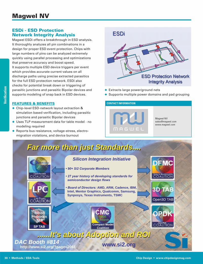
Methods / EDA Tools
CONTACT INFORMATION
Magwel NV
ESDi - ESD Protection Network Integrity Analysis Magwel ESDi offers a breakthrough in ESD analysis.
It thoroughly analyzes all pin combinations in a
design for proper ESD event protection. Chips with
large numbers of pins can be analyzed extremely
quickly using parallel processing and optimizations
that preserve accuracy and boost speed.
It supports multiple ESD device triggers per event
which provides accurate current values on all
discharge paths using precise extracted parasitics
for the full ESD protection network. ESDi also
checks for potential break down or triggering of
parasitic junctions and parasitic Bipolar devices and
supports modeling of snap back in ESD devices.
FEATURES & BENEFITS◆ Chip-level ESD-network layout extraction &
simulation based verification, including parasitic
junctions and parasitic Bipolar devices
◆ Uses TLP measurement data for table model - no
modeling required
◆ Reports bus resistance, voltage-stress, electro-
migration violations, and device burnout
◆ Extracts large power/ground nets
◆ Supports multiple power domains and pad grouping
CONTACT INFORMATION
Magwel NV [email protected] www.magwel.com
www.si2.orgDAC Booth #814http://www.si2.org/?page=2061
Far more than just Standards....Far more than just Standards....
......It’s about Adoption and ROI......It’s about Adoption and ROI
Silicon Integration Initiative
AMD, ARM, Cadence, IBM, Intel, Mentor Graphics, Qualcomm, Samsung, Synposys, Texas Instruments, TSMC
Verification Veri
ficat
ion
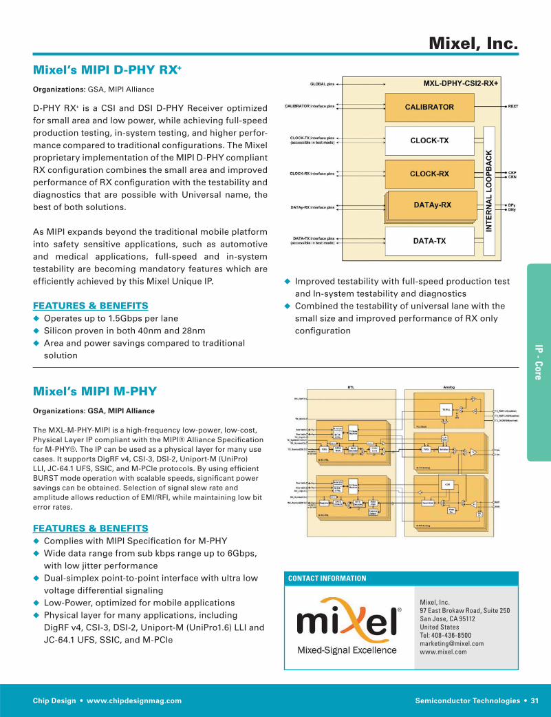
31
CONTACT INFORMATION
IP - Core IP -
Core
Mixel, Inc.
Mixel’s MIPI M-PHY
The MXL-M-PHY-MIPI is a high-frequency low-power, low-cost, Physical Layer IP compliant with the MIPI® Alliance Specification for M-PHY®. The IP can be used as a physical layer for many use cases. It supports DigRF v4, CSI-3, DSI-2, Uniport-M (UniPro) LLI, JC-64.1 UFS, SSIC, and M-PCIe protocols. By using efficient BURST mode operation with scalable speeds, significant power savings can be obtained. Selection of signal slew rate and amplitude allows reduction of EMI/RFI, while maintaining low bit error rates.
FEATURES & BENEFITS◆ Complies with MIPI Specification for M-PHY
◆ Wide data range from sub kbps range up to 6Gbps,
with low jitter performance
◆ Dual-simplex point-to-point interface with ultra low
voltage differential signaling
◆ Low-Power, optimized for mobile applications
◆ Physical layer for many applications, including
DigRF v4, CSI-3, DSI-2, Uniport-M (UniPro1.6) LLI and
JC-64.1 UFS, SSIC, and M-PCIe
Mixel’s MIPI D-PHY RX+ GSA, MIPI Alliance
D-PHY RX+ is a CSI and DSI D-PHY Receiver optimized
for small area and low power, while achieving full-speed
production testing, in-system testing, and higher perfor-
mance compared to traditional configurations. The Mixel
proprietary implementation of the MIPI D-PHY compliant
RX configuration combines the small area and improved
performance of RX configuration with the testability and
diagnostics that are possible with Universal name, the
best of both solutions.
As MIPI expands beyond the traditional mobile platform
into safety sensitive applications, such as automotive
and medical applications, full-speed and in-system
testability are becoming mandatory features which are
efficiently achieved by this Mixel Unique IP.
FEATURES & BENEFITS◆ Operates up to 1.5Gbps per lane
◆ Silicon proven in both 40nm and 28nm
◆ Area and power savings compared to traditional
solution
◆ Improved testability with full-speed production test
and In-system testability and diagnostics
◆ Combined the testability of universal lane with the
small size and improved performance of RX only
configuration
Mixel, Inc.97 East Brokaw Road, Suite 250San Jose, CA 95112United StatesTel: 408-436-8500 [email protected]

CONTACT INFORMATION
ServicesServ
ices
FEATURES & BENEFITS◆ Accepts RF signals from 400 MHz to 4000 MHz
◆ Accepts RF input levels from -60 dBm to -20 dBm
◆ Baseband IF output with up to 390 MHz bandwidth
◆ Internal OCXO or external 10 MHz frequency reference
Available in COTS and rugged PMC/XMC, AMC, VPX,
cPCI, FMC and PCIe formats
APPLICATION AREASCommunications, Radar and Signal Intelligence Systems
AVAILABILITY
Contact Pentek for price and availability at 201-818-5900
or visit http://www.pentek.com/go/em5220
Model 5220Open VPX, PMC/XMC, cPCI, AMC, PCIe,
FMC
Windows & Linux
The Bandit® Model 5220 is a two-channel,
high-performance, stand-alone analog RF wideband
downconverter. Packaged in a small, shielded 3U VPX
board with front-panel connectors for easy integration
into RF systems, the board offers programmable gain,
high dynamic range and a low noise figure.
With an input frequency range from 400 to 4000 MHz and
a wide IF bandwidth of up to 390 MHz, the 5220 is an ideal
solution for amplifying and downconverting antenna
signals for communications, radar and signal intelligence
systems
The 5220 accepts RF signals on two front-panel SSMC
connectors. LNAs (Low Noise Amplifiers) are provided,
along with two programmable attenuators allowing
downconversion of input signals ranging from –60 dBm
to –20 dBm in steps of 0.5 dB. Higher level signals can be
attenuated prior to input.
An optional five-stage lowpass or bandpass input filter
can be included with several available frequency and
attenuation characteristics for RF image rejection and
harmonic suppression.
The 5220 features a pair of Analog Devices ADL5380
quadrature mixers. The ADL5380’s are capable of excel-
lent accuracy with amplitude and phase balances of ~0.07
dB and ~0.2°, respectively.
Locked to an external input reference for accuracy with a
fractional-N phase-locked loop, its frequency is program-
mable across the 400 to the 4000 MHz band with a tuning
resolution of better than 100 kHz. PentekOne Park WayUpper Saddle River NJ, 07458USA201-818-5900 Telephone201-818-5904 [email protected]/go/em5220
Pentek

VIEWPOINT
In the not too distant past –– say 20- to 30 years ago ––
hardware emulators were huge and hulking, with a massive
amount of cables and wires trailing all over the floor. I still
remember my first visit to AMD in Austin, Texas, back in
1995, when I saw Quickturn’s Enterprise Emulation System
emulating a K5 processor. The K5 was AMD’s first x86
processor developed entirely in-house. It was the archetypal
example of “spaghetti syndrome” with thousands of cables
running all over the room without a semblance of structure.
It took an entire engineering team of 10 people to get it set up
and running, and to keep it functioning. Setup times stretched
to weeks or even months past the time first silicon came back
for the foundry, defeating the whole purpose of their existence
and often for pitifully little reward. The sad, often repeated
refrain was: “Time to emulation.”
The cost-of-ownership, including the cost of the machines, the
infrastructure, and the personnel to operate and maintain them
was outrageously expensive, limiting their appeal and viability
to the biggest designs developed at the largest companies
with big pockets. At that time, the cost was $3.5 per gate for
one Enterprise Emulation System box and somewhat less for
multi-box configurations.
The attraction to hardware emulation was unmistakable, even
if they were used only for in circuit emulation (ICE) mode.
What made them appealing was how the pre-silicon design
under test (DUT) could be verified in the post-silicon target
environment at real or quasi-real speed.
All that’s changed in recent years as EDA vendors and
project teams begin to fully realize their value and potential.
Improvements were made with each new generation of
machine. New deployment approaches have been devised; new
verification objectives and applications have been expanding.
The latest generations, then, are ushering in the golden age of
hardware emulation.
Just consider today’s machines are smaller and more cost
effective, despite their increased capacity to accommodate
designs exceeding one billion gates in size. The industry has
moved well beyond loads of cables and wiring to only a few.
The average cost of the machine has lowered to about 1 cent or
so per gate –– more than 100X less expensive than what is was
20 years ago. In fact, it is the least expensive verification tool
when measured in dollars per verification cycle.
At last count, hardware emulation was used in four
different modes, including ICE. The others are embedded
software acceleration, simulation testbench acceleration and
transaction-based acceleration. Some project teams mix and
match modes to meet their purposes.
Which brings me to the next and perhaps most important
reason hardware emulation is enjoying its moment –– its
varied applications and objectives. Hardware emulation can be
used from block- and IP-level testing, to full system validation,
including embedded software validation. The verification
objectives have expanded beyond traditional hardware
debugging, adding functional coverage checking, low-power
verification and power estimation. A new verification territory
is now performance characterization.
The emulation design data center is one more application
that’s getting serious attention from project teams worldwide.
It is built on three technological advances: unmanned remote
access, shared resource, and powerful software management.
Unmanned remote access has been made possible by
the transaction technology and the VirtuaLAB concept
functionally equivalent to ICE. Today, hardware emulation
can be accessed remotely from anywhere in the world, as
simulation server farms used to be for many years. Gone
are the days of AE team in-a-box. In this configuration,
human intervention for connecting/disconnecting external
peripherals is not necessary.
It can also be shared among several teams made up of a
combination of hardware designers, firmware developers,
software engineers located in different time zones and remote
geographies. Advanced job queue management automates,
simplifies and optimizes the allocation of the emulation
resources, essential for managing an expensive piece of capital
equipment as an emulation platform is.
Gone are the days when emulation was a verification tool
few companies could afford and even fewer verification
engineers wanted to use. These days, they’re now basking in
their debugging successes and welcoming the golden age of
hardware emulation.
Lauro Rizzatti is a verification consultant. He was formerly general man-
ager of EVE-USA and its vice president of marketing before Synopsys’
acquisition of EVE. Previously, he held positions in management, product
marketing, technical marketing, and engineering. He can be reached at

For more than 75 years we have been helping you unlock
measurement insights, first as the electronic-measurement
businesses of Hewlett-Packard and Agilent Technologies,
and now, as Keysight Technologies.
From Day 1, there have been two sides to the story. One is
the work we do, creating leading-edge instrumentation and
software. The other is the work you do: designing, developing,
debugging, troubleshooting, manufacturing, testing, installing
and maintaining components, devices and systems.
Those seemingly unrelated activities are actually connected by
something profound: the “A-ha!” that comes with a moment of
insight. When those happen for us, the results are innovations
that help you reach new breakthroughs.
This is our legacy. Keysight is a company built on a history
of firsts, dating back to the days when Bill Hewlett and Dave
Packard worked in the garage at 367 Addison Avenue in Palo Alto,
California. Our firsts began with U.S. patent number 2,268,872
for a “variable-frequency oscillation generator.” Appropriately,
the heart of Bill’s design was a light bulb, which is often used to
symbolize a new idea.
Our future depends on your success, and our vision is simple: by
helping engineers find the right idea at the right time, we enable them
to bring next-generation technologies to their customers—faster.
This is happening in aerospace and defense applications where
increasingly realistic signal simulations are accelerating the
development of advanced systems that protect those who go in
harm’s way. It’s happening in research labs where our tools help
turn scientific discovery into the discovery of new sciences.
It’s taking place with 400G Ethernet and the enabling PAM-4
technology, where our end-to-end solution ranges from simulation
of new designs to characterization of hardware inputs, outputs
and connectors. And in wireless communications we’re providing
leading-edge measurement tools and sophisticated, future-friendly
software that cover all phases of the 5G development cycle.
Within these application areas, there are often more standards
than a single engineer can keep up with. That’s why so many of
our people are involved in standards bodies around the world.
We’re helping shape those standards while creating the tools
needed to meet the toughest performance goals.
Through our global presence, we also have measurement experts
near you: our application engineers have the skills and experience
to help you unite the hardware and software solutions that meet
your unique requirements.
To help Keysight customers continue to open new doors, we’re
concentrating our effort and experience on what comes next in
test and measurement. Our unique combination of hardware,
software and people will help enable your next “A-ha!” moment,
whether you’re working on mobile devices, cloud computing,
semiconductors, renewable energy, or the latest glimmer in your
imagination. Keysight is here to help you see what others can’t,
and then make it reality—sooner.
© Keysight Technologies, Inc. 2015