2013 open access micromachines - mdpi.com · micromachines issn 2072-666x ... chemistry of the...
TRANSCRIPT
Micromachines 2013, 4, 67-79; doi:10.3390/mi4010067
micromachines ISSN 2072-666X
www.mdpi.com/journal/micromachines
Article
Effects of Micromachining Processes on Electro-Osmotic Flow
Mobility of Glass Surfaces
Yosuke Koga 1, Reiko Kuriyama
2, Yohei Sato
2, Koichi Hishida
2 and Norihisa Miki
1,*
1 Department of Mechanical Engineering, Keio University, 3-14-1 Hiyoshi, Kohoku-ku, Yokohama,
Kanagawa, 223-8522, Japan; E-Mail: [email protected] 2 Department of System Design Engineering, Keio University, 3-14-1 Hiyoshi, Kohoku-ku,
Yokohama, Kanagawa, 223-8522, Japan; E-Mails: [email protected] (R.K.);
[email protected] (Y.S.); [email protected] (K.H.)
* Author to whom correspondence should be addressed; E-Mail: [email protected];
Tel.: +81-45-566-1430; Fax: +81-45-566-1495.
Received: 4 January 2013; in revised form: 16 February 2013 / Accepted: 20 February 2013 /
Published: 13 March 2013
Abstract: Silica glass is frequently used as a device material for micro/nano fluidic
devices due to its excellent properties, such as transparency and chemical resistance. Wet
etching by hydrofluoric acid and dry etching by neutral loop discharge (NLD) plasma
etching are currently used to micromachine glass to form micro/nano fluidic channels.
Electro-osmotic flow (EOF) is one of the most effective methods to drive liquids into the
channels. EOF mobility is affected by a property of the micromachined glass surfaces,
which includes surface roughness that is determined by the manufacturing processes. In
this paper, we investigate the effect of micromaching processes on the glass surface
topography and the EOF mobility. We prepared glass surfaces by either wet etching or by
NLD plasma etching, investigated the surface topography using atomic force microscopy,
and attempted to correlate it with EOF generated in the micro-channels of the machined
glass. Experiments revealed that the EOF mobility strongly depends on the surface
roughness, and therefore upon the fabrication process used. A particularly strong
dependency was observed when the surface roughness was on the order of the electric
double layer thickness or below. We believe that the correlation described in this paper can
be of great help in the design of micro/nano fluidic devices.
Keywords: surface roughness; electro-osmotic flow; glass; MicroTAS; nanofluidics; zeta
potential; neutral loop discharge plasma etching; dry etching; wet etching
OPEN ACCESS

Micromachines 2013, 4
68
1. Introduction
Because there are many beneficial size effects at the micro and nano scales, such as short mixing
times, high efficiency in chemical reactions, and minute amounts of reagents and effluent liquids,
micro/nano fluidic devices have been extensively studied for use in biomedical applications [1–20]. In
particular, nano fluidic devices that contain nano channels can be used for separation and filtration [21],
single-molecule detection [22–26], highly efficient PCR [27], chemical analysis [28,29] and
nano-photonic sensors [30], with great help of development of nanofabrication technologies [31–43].
As the channels are reduced in size, the surface roughness and surface chemistry become dominant in
determining the dynamics of flow. Electro-osmotic flow (EOF) is well-known to depend on the surface
chemistry of the channel walls. An electric double-layer is formed near the channel wall, depending on
the wall surface. When an external electric field is applied, the layer moves, generating EOF. Electro-
osmotic pumping is considered to be more efficient in driving liquids in micro/nano channels than
applying differential pressure by an external pump, given the high viscous drag. The wall surface
charge can be quantified by the zeta potential. Therefore, the EOF can be predicted by the given zeta
potential and vice versa. The relationship between the zeta potential and EOF can be described by the
Smoluchowski equation when the surface roughness is smaller than the electric double layer [44–46].
The EOF can be measured by micro-particle image velocimetry (PIV) [47–50]. Fluorescent
nano/micro beads are typically used as tracers, and a confocal microscope can be used to deduce the
velocity distribution in three dimensions [51–59]. Evanescent waves generated by total index reflection
of a laser can be used to derive the velocity near the liquid/wall interface, within approximately 50 nm,
when they are used as the excitation light for the fluorescent tracer particles [60–64].
As we described above, the zeta potential can be calculated from a precisely measured EOF using
the Smoluchowski equation, but this approach cannot be always applied to practical cases. The relation
was modified for non-wetting charged surfaces by considering the fluid slip effect [65], which was
experimentally validated [66]. Surface roughness is another factor that needs to be taken into
consideration. Since surface roughness does affect EOF, this leads to errors in the zeta potential. On
the other hand, even though the zeta potential of the channel wall material was known, it cannot
accurately predict the resulting EOF in manufactured nano channels due to the surface roughness.
The surface roughness depends on the manufacturing process [67]. For example, glass, one of the
most commonly used materials due to its superior chemical resistivity and transparency, can be
patterned by wet etching using hydrofluoric acid (HF), dry etching, or mechanical machining. Wet
etching is an isotropic technique but can be conducted at low cost. Dry etching can create anisotropic
profiles with a high accuracy and a high aspect ratio. Mechanical machining can be used to fabricate
three-dimensional structures. Each etching process culminates in a different surface geometry,
depending on the etching conditions.
In this work, we attempted to experimentally obtain the EOF mobility, which is affected by both
surface roughness and surface chemistry. The surface roughness is strongly affected by the
manufacturing method and etching conditions. We prepared glass channels by wet etching and dry
etching using various recipes, and formed micro-channels by attaching micropatterned polydimethyl
siloxane (PDMS). We measured the EOF near the glass surface using microPIV, and the glass surface
geometry was investigated by atomic force microscopy (AFM). We attempted to correlate the surface

Micromachines 2013, 4
69
topography, and thus, the micromaching processes, with the EOF mobility. Since the Smoluchowski
equation can be used to deduce the zeta potential only when the roughness is smaller than the electric
double layer thickness, the EOF mobility obtained in the experiments cannot provide the true zeta
potential that represents the chemical properties of the surface. Instead, we discuss the potential usage
of an effective zeta potential, which is obtained by substituting the EOF mobility into the
Smoluchowski equation and depends on both the chemical and topographical properties of the surface.
When the effective zeta potential of micromachined glass surfaces is known, the EOF can be deduced
using the Smoluchowski equation. The obtained data will be of great help in precisely designing high-
performance nano/micro fluidic devices.
2. Material and Method
2.1. Micromachining of Glass Substrates
In our experiments, we used borosilicate glass (C030401, Matsunami Glass Ind., Ltd., Osaka, Japan)
as the wall material. Hydrofluoric acid (HF) was purchased from Wako Pure Chemical Industries, Ltd.,
Osaka, Japan. Plasma etching of glass was conducted by NLD-570 (Ulvac, Inc., Kanagawa, Japan).
The surface geometry after the machining process was investigated by atomic force microscopy
(SPM-9700, Shimadzu, Kyoto, Japan).
The most frequently used glass manufacturing method is wet etching by HF. HF can pattern glass
by the following reaction;
SiO2 + 6HF → H2SiF6 + 2H20 (1)
We conducted two experiments. First, we fixed the etching depth at 10 µm and used HF with
concentrations of 1%, 3%, 5%, 7%, and 9%. The required etching periods were 5460, 1500, 580, 330,
and 280 s, respectively. In the second experiment, glass substrates were immersed in 5% HF for 5, 10,
15, 20, or 25 min. The etching was conducted in a cleanroom environment at 25 °C and 40% Rh. We
prepared five samples for each condition. Note that in these experiments, the whole surfaces were
etched, i.e., no mask pattern was used.
While deep reactive ion etching of silicon has been extensively used in manufacturing MEMS for
decades [68,69], the etching of glass using neutral loop discharge (NLD) is a promising technology for
manufacturing glass micro/nano structures [70–73]. NLD employs plasma generated along a closed
magnetic neutral line by a radio frequency (RF) electric field. NLD plasma has a high plasma density
at a relatively low gas pressure, and can be applicable to high-aspect-ratio anisotropic etching.
In our experiments, borosilicate glass plates were etched by NLD-570 while they were attached to a
6-inch silicon carbide wafer with a silicone oil compound to dissipate heat during the etching. We
varied the antenna power to be 250, 500, 1200, or 1800 W. The etching periods were controlled to
achieve 5-μm-deep patterns, which led to 5880, 3840, 1800, or 1560 s etch times, respectively. Other
representative etching parameters are: APC pressure of 0.4 Pa, trigger pressure of 1 Pa, PFC pressure
of 400 Pa, both gas flow rates of C3F8 and CHF3 of 10 sccm, bias RF power of 300 W, currents for
magnet top, middle, and bottom of 12.2 A, 17 A, 12.2 A, respectively. We prepared five samples for
each condition. Note that in these experiments, the whole surfaces were etched, i.e., no mask pattern
was used.
Micromachines 2013, 4
70
The surface geometry was investigated by atomic force microscopy SPM-9700after the machining
process. 10 measurement areas 10 µm by 10 µm in size were randomly selected from each sample.
2.2. Measurement of EOF
The EOF velocity was measured by micro PIV. When charged tracing particles are used for the
measurement, the measured velocity is the summation of EOF and electrophoretic flow velocities [56].
The electrophoretic velocity under the identical measurement conditions was obtained in advance and
then, subtracted from the measured velocity by micro PIV to deduce the EOF velocity.
First, as described above, glass plates were micromachined by either wet etching with HF or dry
etching using NLD plasma. Note that these etching processes created no patterns on the glass surfaces.
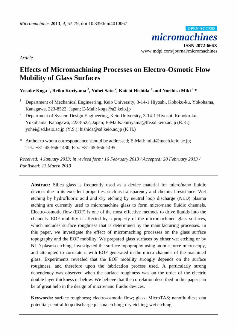
A polydimethyl siloxane (PDMS, Silpot 184, Toray, Tokyo, Japan) structure with a channel 1 mm in
width, 30 mm in length, and 100 µm in height and inlet/outlet holes molded from photolithography
patterned SU-8 (SU-8 3000, Nippon Kayaku, Tokyo, Japan) was bonded onto the glass plates after
oxygen plasma treatment, as shown in Figure 1. Fluorescent micro beads 0.2 µm in diameter
(FluoSpheres carboxylate-modified microspheres 0.2 µm yellow-green fluorescent, Molecular Probes,
Inc., Eugene, OR, USA) were used as the tracing particles. These beads were excited by a laser with a
wavelength of 505 nm, and emitted fluorescence at 515 nm. 0.5 mL of carboxylate solution containing
2wt% of microbeads was mixed with 99.5 mL of deionized water. Then, this solution was mixed with
a solution containing 1 Ml of 1 M HEPES (4-(2-hydroxyethyl)-1-piperazineethanesulfonic acid), 1 mL
of 0.1 M KCl, and 98 mL of deionized water. We introduced this 0.005% fluorescent micro-bead
solution into the channel. An electric field of 13.3 V/mm was applied and an EOF was generated. The
experiments were conducted at 25 °C and 40% Rh. pH of the fluorescent solution was 7.15 and the
produced electric double layer thickness was calculated to be 30.2 nm under these conditions. The
velocity at the center of the channel in the horizontal plane and 5 µm above the glass surface was
measured by micro-PIV. Though three channel walls were made of PDMS, the EOF generated near the
glass surface was determined by the characteristics of the glass surface [56]. In order to prevent
electrolysis, the measurement started 2 s after the electric field was applied and the measurement time
was limited to be 2 s. Note that we experimentally confirmed that the EOF became steady 1 s after the
field was applied. The micro PIV measurement was conducted one time for a sample since it was
difficult to wash out all the tracing particles from the channel after each measurement, i.e., 5 EOF
velocity data were obtained for one machining condition.
Figure 1. A micro-channel used to evaluate the electro-osmotic flow (EOF).
Micromachines 2013, 4
71
3. Experiments
3.1. Surface Roughness after Glass Patterning
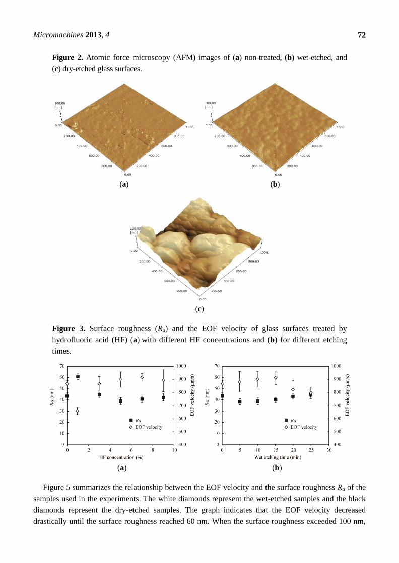
Figure 2 shows surface topography images of untreated glass, glass wet-etched by 5 µm, and glass
dry-etched by 5 µm obtained by AFM. Dry etching using NLD plasma drastically increased the surface
roughness, while wet etching did not. In wet etching using HF, the concentration of HF did not affect
the surface roughness, as represented by the arithmetic mean value Ra except the case of 1%
concentration, as shown in Figure 3a. Ra of the non-treated glass surface was 43 nm, while that of the
glass treated by 1% HF was 61 nm. This was most likely caused by the long wet etching time required
by 1% HF of 5460 s to achieve an etching depth of 10 µm. When 5% HF was used as the etchant, the
surface roughness decreased in the first 15 min of etching, which was a nature of isotropic wet etching.
The surface roughness increased slightly when the etching time was greater than 20 min as shown in
Figure 3b.
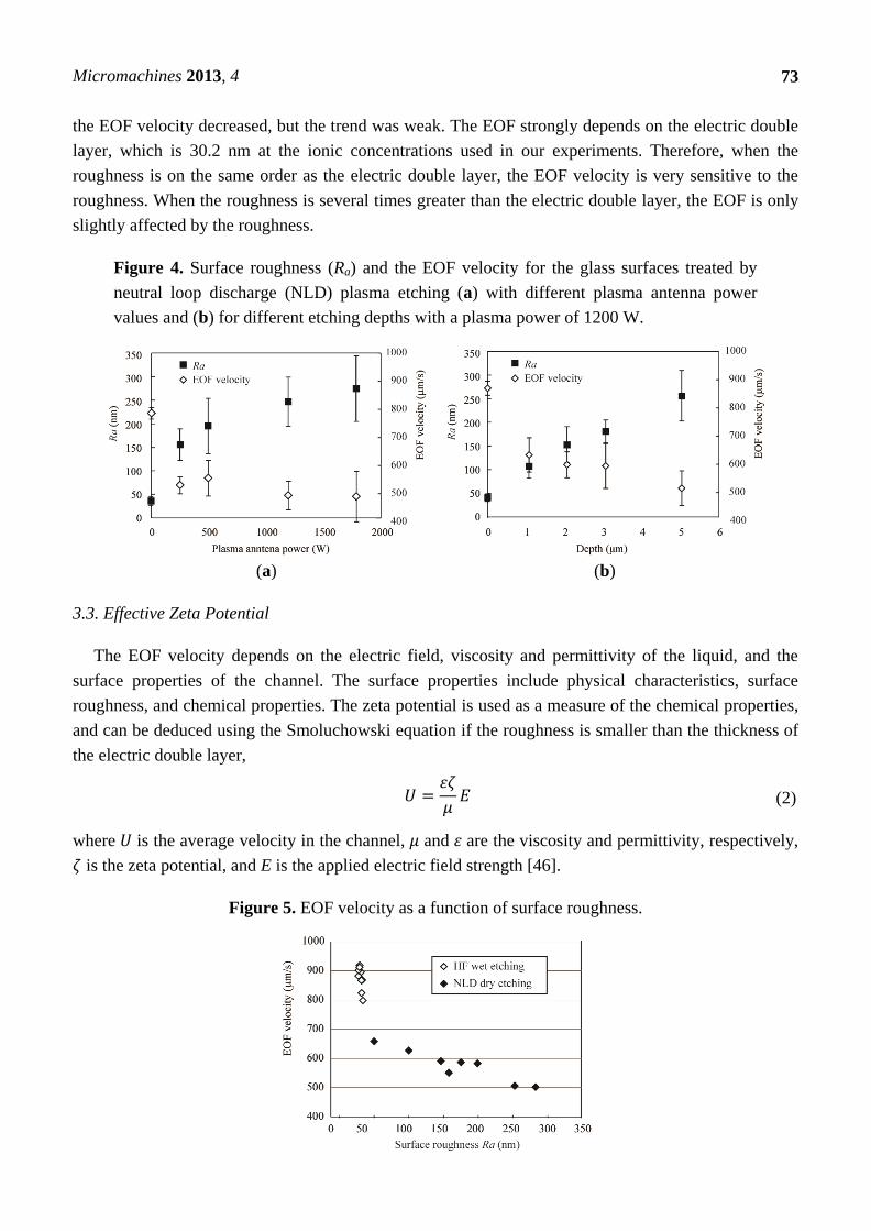
On the contrary, Ra of the surface etched by NLD plasma strongly depended on the plasma power
when we fixed the etching depth at 5 µm, as shown in Figure 4a. Ra increased from approximately 160
nm to 280 nm when the plasma power was increased from 250 W to 1800 W. For a plasma power of
1200 W, Ra increased from 40 nm to 210 nm as the etching progressed, as shown in Figure 4b.
3.2. EOF Measurement
The EOF velocity generated in channels with glass surfaces treated by wet etching is summarized in
Figure 3. Figure 3a shows the surface roughness and EOF velocity for glass substrates etched by 10
µm using different concentrations of HF. The glass substrate treated by 1% HF generated an EOF
velocity of 660 µm/s, while the non-treated glass substrate generated an EOF velocity of 870 µm/s.
Figure 3b shows the relationship between the etching time by 5% HF and the EOF velocity. In both
graphs, the EOF velocity decreased with increasing surface roughness, and there was a strong
correlation between surface roughness and EOF velocity.
For dry-etched samples, as shown in Figure 4, the EOF velocity decreased as the roughness
increased, although the trend was not as strong as with the wet-etched samples. Figure 4a shows EOF
velocities for glass substrates etched by 5 µm with various antenna RF power values in NLD etching.
The etching time was controlled to achieve a depth of 5 µm. 0 W corresponds to a non-treated glass
substrate. The EOF velocity slightly decreased with increasing power, and was 500 µm/s at 1800 W.
The EOF velocity as a function of etching depth at 1200 W is shown in Figure 4b. The EOF velocity
decreased with increasing time, and reached 510 µm/s at a depth of 5 µm.
Micromachines 2013, 4
72
Figure 2. Atomic force microscopy (AFM) images of (a) non-treated, (b) wet-etched, and
(c) dry-etched glass surfaces.
(a) (b)
(c)
Figure 3. Surface roughness (Ra) and the EOF velocity of glass surfaces treated by
hydrofluoric acid (HF) (a) with different HF concentrations and (b) for different etching
times.
(a) (b)
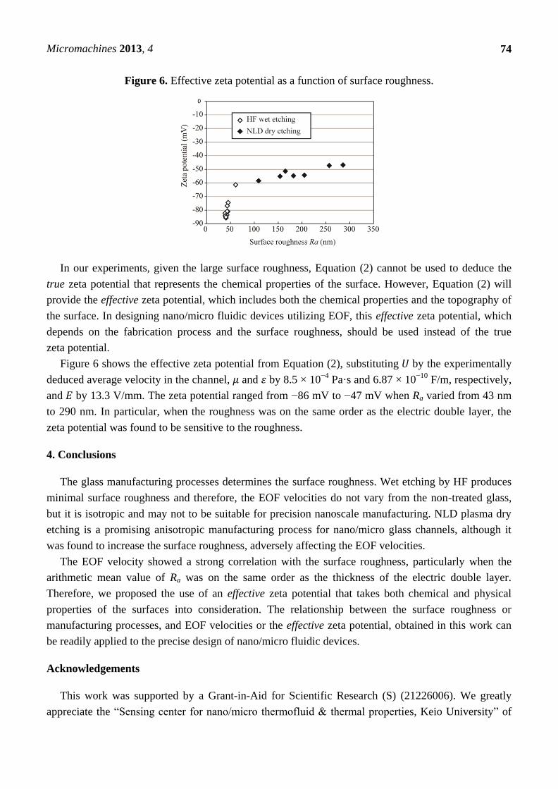
Figure 5 summarizes the relationship between the EOF velocity and the surface roughness Ra of the
samples used in the experiments. The white diamonds represent the wet-etched samples and the black
diamonds represent the dry-etched samples. The graph indicates that the EOF velocity decreased
drastically until the surface roughness reached 60 nm. When the surface roughness exceeded 100 nm,
Micromachines 2013, 4
73
the EOF velocity decreased, but the trend was weak. The EOF strongly depends on the electric double
layer, which is 30.2 nm at the ionic concentrations used in our experiments. Therefore, when the
roughness is on the same order as the electric double layer, the EOF velocity is very sensitive to the
roughness. When the roughness is several times greater than the electric double layer, the EOF is only
slightly affected by the roughness.
Figure 4. Surface roughness (Ra) and the EOF velocity for the glass surfaces treated by
neutral loop discharge (NLD) plasma etching (a) with different plasma antenna power
values and (b) for different etching depths with a plasma power of 1200 W.
(a) (b)
3.3. Effective Zeta Potential
The EOF velocity depends on the electric field, viscosity and permittivity of the liquid, and the
surface properties of the channel. The surface properties include physical characteristics, surface
roughness, and chemical properties. The zeta potential is used as a measure of the chemical properties,
and can be deduced using the Smoluchowski equation if the roughness is smaller than the thickness of
the electric double layer,
(2)
where is the average velocity in the channel, and are the viscosity and permittivity, respectively,
is the zeta potential, and E is the applied electric field strength [46].
Figure 5. EOF velocity as a function of surface roughness.
Micromachines 2013, 4
74
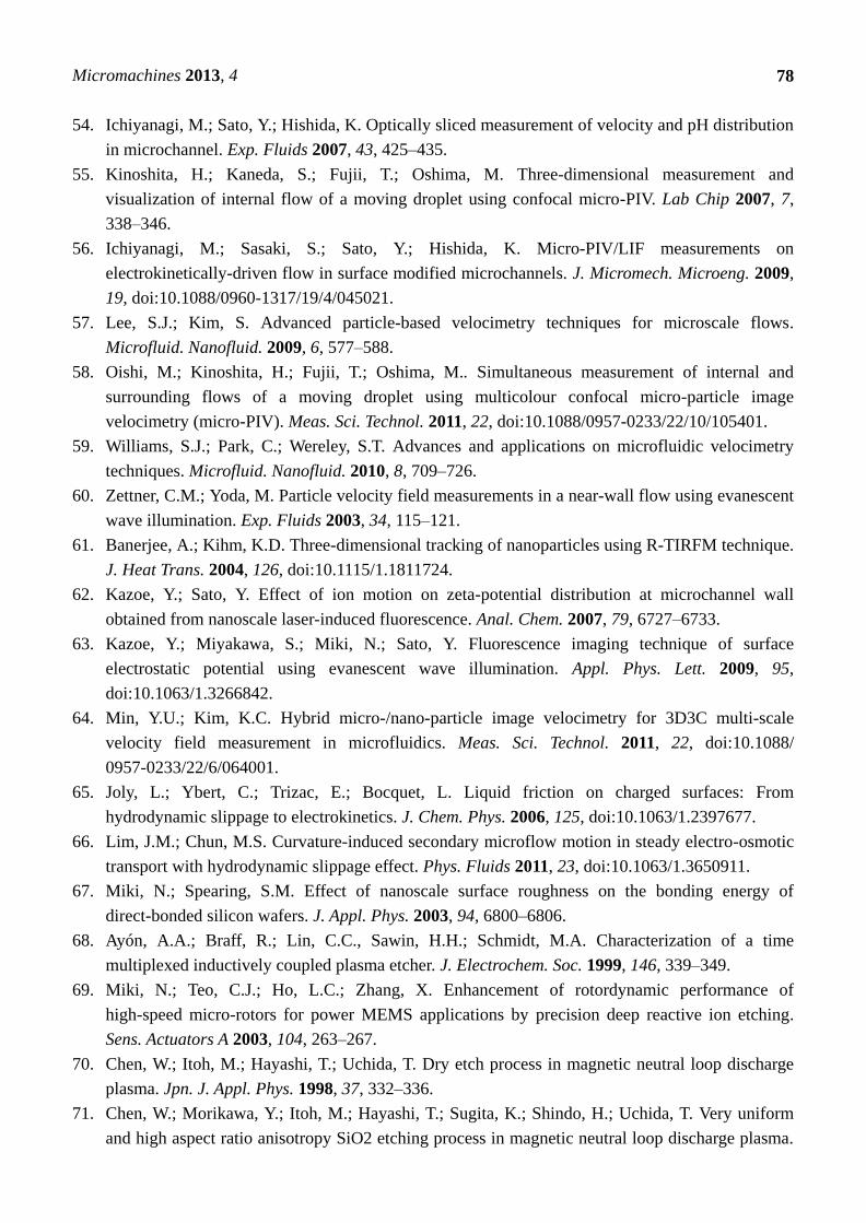
Figure 6. Effective zeta potential as a function of surface roughness.
In our experiments, given the large surface roughness, Equation (2) cannot be used to deduce the
true zeta potential that represents the chemical properties of the surface. However, Equation (2) will
provide the effective zeta potential, which includes both the chemical properties and the topography of
the surface. In designing nano/micro fluidic devices utilizing EOF, this effective zeta potential, which
depends on the fabrication process and the surface roughness, should be used instead of the true
zeta potential.
Figure 6 shows the effective zeta potential from Equation (2), substituting by the experimentally
deduced average velocity in the channel, and by 8.5 × 10⁻⁴
Pa·s and 6.87 × 10⁻¹⁰
F/m, respectively,
and by 13.3 V/mm. The zeta potential ranged from −86 mV to −47 mV when Ra varied from 43 nm
to 290 nm. In particular, when the roughness was on the same order as the electric double layer, the
zeta potential was found to be sensitive to the roughness.
4. Conclusions
The glass manufacturing processes determines the surface roughness. Wet etching by HF produces
minimal surface roughness and therefore, the EOF velocities do not vary from the non-treated glass,
but it is isotropic and may not to be suitable for precision nanoscale manufacturing. NLD plasma dry
etching is a promising anisotropic manufacturing process for nano/micro glass channels, although it
was found to increase the surface roughness, adversely affecting the EOF velocities.
The EOF velocity showed a strong correlation with the surface roughness, particularly when the
arithmetic mean value of Ra was on the same order as the thickness of the electric double layer.
Therefore, we proposed the use of an effective zeta potential that takes both chemical and physical
properties of the surfaces into consideration. The relationship between the surface roughness or
manufacturing processes, and EOF velocities or the effective zeta potential, obtained in this work can
be readily applied to the precise design of nano/micro fluidic devices.
Acknowledgements
This work was supported by a Grant-in-Aid for Scientific Research (S) (21226006). We greatly
appreciate the “Sensing center for nano/micro thermofluid & thermal properties, Keio University” of

Micromachines 2013, 4
75
“Low-Carbon Research Network” funded by the Ministry of Education, Culture, Sports, Science and
Technology (MEXT), Japan for the microPIV system.
References
1. Manz, A.; Graver, N.; Widmer, H.M. Miniaturized total chemical-analysis systems—a novel
concept for chemical sensing. Sens. Actuators B 1990, 1, 244–248.
2. Shoji, S. Fluids for sensor systems. Top. Curr. Chem. 1998, 194, 163–188.
3. Khandurina, J.; Guttman, A. Bioanalysis in microfluidic devices. J. Chromatogr. A 2002, 943,
159–183.
4. Chovan, T.; Guttman, A. Microfabricated devices in biotechnology and biochemical processing.
Trends Biotechnol. 2002, 20, 116–122.
5. Huikko, K.; Kostiainen, R.; Kotiaho, T. Introduction to micro-analytical systems: Bioanalytical
and pharmaceutical applications. Eur. J. Pharm. Sci. 2003, 20, 149–171.
6. Sheehan, A.D.; Quinn, J.; Daly, S.; Dillon, P.; O’Kennedy, R. The development of novel
miniaturized immuno-sensing devices: A review of a small technology with a large future. Anal.
Lett. 2003, 36, 511–537.
7. Sato, K.; Hibara, A.; Tokeshi, M.; Hisamoto, H.; Kitamori, T. Microchip-based chemical and
biochemical analysis systems. Adv. Drug Deliv. Rev. 2003, 55, 379–391.
8. Lee, S.J.; Lee, S.Y. Micro total analysis system (mu-TAS) in biotechnology. Appl. Microbiol. Biot.
2004, 64, 289–299.
9. Sun, Y.; Kwok, Y.C. Polymeric microfluidic system for DNA analysis. Anal. Chim. Acta 2006,
556, 80–96.
10. Gu, Y.; Miki, N. A microfilter utilizing a polyethersulfone porous membrane with nanopores. J.
Micromech. Microeng. 2007, 17, 2308–2315
11. Tanaka, Y.; Sato, K.; Shimizu, T.; Yamato, M.; Okano, T.; Kitamori, T. Biological cells on
microchips: New technologies and applications. Biosens. Bioelectron. 2007, 23, 449-458.
12. Chen, Y.; Wang, X.H.; Hong, M.; Erramilli, S.; Mohanty, P. Surface-modified silicon nano-
channel for urea sensing. Sens. Actuators 2008, 133, 593–598.
13. Suzuki, H.; Takeuchi, S. Microtechnologies for membrane protein studies. Anal. Bioanal. Chem.
2008, 391, 2695–2702.
14. Gu, Y.; Miki, N. Multilayered microfilter using a nanoporous PES membrane and applicable as
the dialyzer of a wearable artificial kidney. J. Micromech. Microeng. 2009, 19, doi:10.1088/
0960-1317/19/6/065031.
15. Xu, X.; Zhang, S.; Chen, H.; Kong, J. Integration of electrochemistry in micro-total analysis
systems for biochemical assays: Recent developments. Talanta 2009, 80, 8–18.
16. Ota, H.; Yamamoto, R.; Deguchi, K.; Tanaka, Y.; Kazoe, Y.; Sato, Y.; Miki, N. Three-dimensional
spheroid-forming lab-on-a-chip using micro-rotational flow. Sens. Actuators B 2010, 147, 359–365.
17. Liu, K.K.; Wu, R.G.; Chuang, Y.J.; Khoo, H.S.; Huang, S-H.; Tseng, F-G. Microfluidic systems
for biosensing. Sensors 2010, 10, 6623–6661.
18. Wlodkowic, D.; Cooper, J.M. Tumors on chips: Oncology meets microfluidics. Curr. Opin. Chem.
Biol. 2010, 14, 556–567.

Micromachines 2013, 4
76
19. Ota, H.; Kodama, T.; Miki, N. Rapid formation of size-controlled three dimensional hetero-cell
aggregates using micro-rotation flow for spheroid study. Biomicrofluidics 2011, 5,
doi:10.1063/1.3609969.
20. Ota, H.; Miki, N. Microfluidic experimental platform for producing size-controlled
three-dimensional spheroids. Sens. Actuators A 2011, 169, 266–273.
21. Shen, C.; Mokkapati, V.R.S.S.; Pham, H.T.M.; Sarro, P.M. Micromachined nanofiltration modules for
lab-on-a-chip applications. J. Micromech. Microeng. 2012, 22, doi:10.1088/0960-1317/22/2/025003.
22. Wang, K.; Yue, S.; Wang, L.; Jin, A.; Gu, C.; Wang, P.; Wang, H.; Xu, X.; Wang, Y.; Niu, H.
Nanofluidic channels fabrication and manipulation of DNA molecules. IEEE Proc.
Nanobiotechnol. 2006, 153, 11–15.
23. Das, S.K.; Austin, M.D.; Akana, M.C.; Deshpande, P.; Cao, H.; Xiao, M. Single molecule linear
analysis of DNA in nano-channel labeled with sequence specific fluorescent probles. Nucleic
Acids Res. 2010, 38, doi:10.1093/nar/gkq673.
24. Liu, C.; Qu, Y.Y.; Luo, Y.; Fang, N. Recent advances in single-molecule detection on micro- and
nano-fluidic devices. Electrophoresis 2011, 32, 3308–3318.
25. Kish, L.L.; Kameoka, J.; Granqvist, C.G.; Kish, L.B. Log-normal distribution of single molecule
fluorescence bursts in micro/nano-fluidic channels. Appl. Phys. Lett. 2011, 99, doi:10.1063/1.3648118.
26. Abad, E.; Juarros, A.; Retolaza, A.; Merino, S.; Marie, R.; Kristensen, A. DNA analysis by single
molecule stretching in nanofluidic biochips. Microelectron. Eng. 2011, 88, 300–304.
27. Eun, D.S.; Shin, J.K.; Lee, J.H. Enhanced micro-PCR chip using TiO2nanofluidic heat-sink. Sens.
Lett. 2009, 9, 276–282.
28. Chen, P.; Feng, X.; Du, W.; Liu, B-F. Microfluidic chips for cell sorting. Front. Biosci. 2008, 13,
2464–2483.
29. Mawatari, K.; Tsukahara, T.; Sugii, Y.; Kitamori, T. Extended-nano fluidic systems for analytical
and chemical technologies. Nanoscale 2010, 2, 1588–1595.
30. Huang, M.; Yanik, A.A.; Chang, T.Y.; Altug, H. Sub-wavelength nanofluidics in photonic crystal
sensors. Opt. Express 2009, 17, 24224–24233.
31. Cao, H.; Yu, Z.N.; Wang, J.; Tegenfeldt, J.O.; Austin, R.H.; Chen, E.; Wu, W.; Chou, S.Y.
Fabrication of 10 nm enclosed nanofluidic channels. Appl. Phys. Lett. 2002, 81, 174–176
32. Pepin, A.; Youninou, P.; Studer, V.; Lebib, A.; Chen, Y. Nanoimprint lithography for the
fabrication of DNA electrophoresis chips. Microelectron. Eng. 2002, 61, 927–932.
33. Zheng, H.J.; Wang, Z.L.; Feinerman, A.D. Fabrication of micro/nano fluidic channels with
sacrificial galvanic coupled metals. Nanotechnology 2006, 17, 3183–3188.
34. Shao, P.E.; van Kan, A.; Wang, L.P.; Ansari, K.; Bettiol, A.A.; Watt, F. Fabrication of enclosed
nanochannels in poly(methylmethacrylate) using proton beam writing and thermal bonding. Appl.
Phys. Lett. 2006, 88, doi:10.1063/1.2181631.
35. Kehagias, N.; Chansin, G.; Reboud, V.; Zelsmann, M.; Schuster, C.; Kubenz, M.; Reuther, F.;
Gruetzner, G.; Sotomayer Torres, C.M. Embedded nano channels fabricated by non-selective
reverse contact UV nanoimprint lithography technique. Microelectron. Eng. 2007, 84, 921–924.
36. Wong, C.C.; Agarwal, A.; Balasubramanian, N.; Kwong, D.L. Fabrication of self-sealed circular
nano/microfluidic channels in glass substrates. Nanotechnology 2007, 18, doi:10.1088/0957-4484/
18/13/135304.

Micromachines 2013, 4
77
37. Koller, D.M.; Galler, N.; Ditlbacher, H.; Hohenau, A.; Leitner, A.; Aussenegg, F.R.; Kren, J.R.
Direct fabrication of micro/nano fluidic channels by electron beam lithography. Microelectron.
Eng. 2009, 86, 1314–1316.
38. Yang, R.; Lu, B.R.; Wang, J.; Xie, S-Q.; Chen, Y.; Hug, E.; Qu, X-P.; Liu, R. Fabrication of
micro/nano fluidic channels by nanoimprint lithography and bonding using SU-8. Microelectron.
Eng. 2009, 86, 1379–1381.
39. Venkatakrishnan, K.; Jariwala, S.; Tan, B. Maskless fabrication of nano-fluidic channels by
two-photon absorption (TPA) polymerization of SU-8 on glass substrate. Opt. Express 2009, 17,
2756–2762.
40. Kim, S.K.; Cho, H.; Park, H.K.; Kim, J.H.; Chung, B.H. Fabrication of nanochannels by
anisotropic wet etching on silicon-on-insulator wafers and their applications to DNA stretch. J.
Nanosci. Nanotechnol. 2010, 10, 637–642.
41. Fernandez-Cuesta, I.; Palmarelli, A.L.; Liang, X.G.; Zhang, J.; Dhuey, S.; Olynick, D.; Cabrini, S.
Fabrication of fluidic devices with 30 nm nanochannels by direct imprinting. J. Vac. Sci. Technol.
B 2011, 29, doi:10.1116/1.3662886.
42. Afanasiev, A.; Lahdesmaki, I.; Parviz, B.A. Fabrication and electrical characterization of
integrated nano-scale fluidic channels. Microsyst. Technol. 2011, 17, 1511–1518.
43. Hong, L.F.; Pan, T.R. Surface microfluidics fabricated by photopatternable superhydrophobic
nanocomposite. Microfluid. Nanofluid. 2011, 10, 991–997.
44. Hunter, R.J. Zeta potential in Colloid Science: Principles and Applications; Academic Press: New
York, NY, US, 1981.
45. Sze, A.; Erickson, D.; Ren, L. Zeta-potential measurement using the Smoluchowski equation and the
slope of the current-time relationship in electrosmotic flow. J. Colloid Interf. Sci. 2003, 261, 402–410.
46. Venditti, R.; Xuan, X.C.; Li, D.Q. Experimental characterization of the temperature dependence of
zeta potential and its effect on electroosmotic flow velocity in microchannels. Microfluid.
Nanofluid. 2006, 2, 493–499.
47. Santiago, J.G.; Wereley, S.T.; Meinhart, C.D.; Beebe, D.J.; Adrian, R.J. A particle image
velocimetry system for microfluidics. Exp. Fluids 1998, 25, 316–319.
48. Sato, Y.; Hishida, K. Electrokinetic effects on motion of submicron particles in microchannel.
Fluid Dyn. Res. 2006, 38, 787–802.
49. Lindken, R.; Rossi, M.; Grosse, S.; Westerweel, J. Micro-Particle Image Velocimetry (mu PIV):
Recent developments, applications, and guidelines. Lab Chip 2009, 9, 2551–2567.
50. Tatsumi, K.; Nishitani, K.; Fukuda, K.; Katsumoto, Y.; Nakabe, K. Measurement of
electroosmotic flow velocity and electric field in microchannels by micro-particle image
velocimetry. Meas. Sci. Technol. 2010, 21, doi:10.1088/0957-0233/21/10/105402.
51. Park, J.S.; Choi, C.K.; Kihm, K.D. Optically sliced micro-PIV using confocal laser scanning
microscopy (CLSM). Exp. Fluids 2004, 37, 105–119.
52. Lima, R.; Wada, S.; Tsubota, K.; Yamaguchi, T. Confocal micro-PIV measurements of three-
dimensional profiles of cell suspension flow in a square microchannel. Meas. Sci. Technol. 2006,
17, 797–808.
53. Park, J.S.; Kihm, K.D. Use of confocal laser scanning microscopy (CLSM) for depthwise
resolved microscale-particle image velocimetry (µ-PIV). Opt. Lasers Eng. 2006, 44, 208–223.
Micromachines 2013, 4
78
54. Ichiyanagi, M.; Sato, Y.; Hishida, K. Optically sliced measurement of velocity and pH distribution
in microchannel. Exp. Fluids 2007, 43, 425–435.
55. Kinoshita, H.; Kaneda, S.; Fujii, T.; Oshima, M. Three-dimensional measurement and
visualization of internal flow of a moving droplet using confocal micro-PIV. Lab Chip 2007, 7,
338–346.
56. Ichiyanagi, M.; Sasaki, S.; Sato, Y.; Hishida, K. Micro-PIV/LIF measurements on
electrokinetically-driven flow in surface modified microchannels. J. Micromech. Microeng. 2009,
19, doi:10.1088/0960-1317/19/4/045021.
57. Lee, S.J.; Kim, S. Advanced particle-based velocimetry techniques for microscale flows.
Microfluid. Nanofluid. 2009, 6, 577–588.
58. Oishi, M.; Kinoshita, H.; Fujii, T.; Oshima, M.. Simultaneous measurement of internal and
surrounding flows of a moving droplet using multicolour confocal micro-particle image
velocimetry (micro-PIV). Meas. Sci. Technol. 2011, 22, doi:10.1088/0957-0233/22/10/105401.
59. Williams, S.J.; Park, C.; Wereley, S.T. Advances and applications on microfluidic velocimetry
techniques. Microfluid. Nanofluid. 2010, 8, 709–726.
60. Zettner, C.M.; Yoda, M. Particle velocity field measurements in a near-wall flow using evanescent
wave illumination. Exp. Fluids 2003, 34, 115–121.
61. Banerjee, A.; Kihm, K.D. Three-dimensional tracking of nanoparticles using R-TIRFM technique.
J. Heat Trans. 2004, 126, doi:10.1115/1.1811724.
62. Kazoe, Y.; Sato, Y. Effect of ion motion on zeta-potential distribution at microchannel wall
obtained from nanoscale laser-induced fluorescence. Anal. Chem. 2007, 79, 6727–6733.
63. Kazoe, Y.; Miyakawa, S.; Miki, N.; Sato, Y. Fluorescence imaging technique of surface
electrostatic potential using evanescent wave illumination. Appl. Phys. Lett. 2009, 95,
doi:10.1063/1.3266842.
64. Min, Y.U.; Kim, K.C. Hybrid micro-/nano-particle image velocimetry for 3D3C multi-scale
velocity field measurement in microfluidics. Meas. Sci. Technol. 2011, 22, doi:10.1088/
0957-0233/22/6/064001.
65. Joly, L.; Ybert, C.; Trizac, E.; Bocquet, L. Liquid friction on charged surfaces: From
hydrodynamic slippage to electrokinetics. J. Chem. Phys. 2006, 125, doi:10.1063/1.2397677.
66. Lim, J.M.; Chun, M.S. Curvature-induced secondary microflow motion in steady electro-osmotic
transport with hydrodynamic slippage effect. Phys. Fluids 2011, 23, doi:10.1063/1.3650911.
67. Miki, N.; Spearing, S.M. Effect of nanoscale surface roughness on the bonding energy of
direct-bonded silicon wafers. J. Appl. Phys. 2003, 94, 6800–6806.
68. Ayón, A.A.; Braff, R.; Lin, C.C., Sawin, H.H.; Schmidt, M.A. Characterization of a time
multiplexed inductively coupled plasma etcher. J. Electrochem. Soc. 1999, 146, 339–349.
69. Miki, N.; Teo, C.J.; Ho, L.C.; Zhang, X. Enhancement of rotordynamic performance of
high-speed micro-rotors for power MEMS applications by precision deep reactive ion etching.
Sens. Actuators A 2003, 104, 263–267.
70. Chen, W.; Itoh, M.; Hayashi, T.; Uchida, T. Dry etch process in magnetic neutral loop discharge
plasma. Jpn. J. Appl. Phys. 1998, 37, 332–336.
71. Chen, W.; Morikawa, Y.; Itoh, M.; Hayashi, T.; Sugita, K.; Shindo, H.; Uchida, T. Very uniform
and high aspect ratio anisotropy SiO2 etching process in magnetic neutral loop discharge plasma.

Micromachines 2013, 4
79
J. Vac. Sci. Technol. A 1999, 17, 2546–2550.
72. Chen, W.; Sugita, K.; Morikawa, Y.; Yasunami, S.; Hayashi, T.; Uchida, T. Application of
magnetic neutral loop discharge plasma in deep silica etching. J. Vac. Sci. Technol. A 2001, 19,
2936–2940.
73. Uchida, T.; Hamaguchi, S. Magnetic neutral loop discharge (NLD) plasmas for surface processing.
J. Phys. D 2008, 41, doi:10.1088/0022-3727/41/8/083001.
© 2013 by the authors; licensee MDPI, Basel, Switzerland. This article is an open access article
distributed under the terms and conditions of the Creative Commons Attribution license
(http://creativecommons.org/licenses/by/3.0/).