2009 summer meeting of the avs hudson … analysis in the semiconductor industry by time-of-flight...
TRANSCRIPT
2009 SUMMER MEETING of the AVS HUDSON MOHAWK CHAPTER
Tuesday, June 23, 2009 3-7pm, Holiday Inn Turf 205 Wolf Rd., Albany NY
Phone: 518-458-7250
3pm – Brief Opening Remarks Talks 3:00 T1 Brian Scherer GE-GRC THE PLASMA ENHANCED CHEMICAL VAPOR DEPOSITION AND PERFORMANCE OF A GRADED ULTRA-HIGH GAS BARRIER COATING 3:20 T2 Jasmeet Chawla RPI ELECTRON SCATTERING AT SINGLE CRYSTAL Cu(001) SURFACES 3:40 T3 Albert. Schnieders Tascon USA DEFECT ANALYSIS IN THE SEMICONDUCTOR INDUSTRY BY TIME-OF-FLIGHT SECONDARY ION MASS SPECTROMETRY 4:00 T4 Srijit Mukherjee RPI TEMPERATURE DRIVEN ANOMALOUS SCALING DURING GLANCING ANGLE DEPOSITION 4:20 T5 Eric Bersch College for Nanoscale Science & Engineering X-RAY PHOTOEMISSION SPECTROSCOPY AND SPECTROSCOPIC ELLIPSOMETRY CHARACTERIZATION OF HFO2 AND HAFNIUM SILICATE FILMS ON SiO2/Si 4:40 T6 David Surman Kratos INVESTIGATION INTO THE PARAMETERS INFLUENCING XPS SPUTTER DEPTH PROFILING USING POLYCYCLIC AROMATIC HYDROCARBONS.

Poster Session 5-7pm with Pizza and Cash Bar P1 Ruqiang Bao RPI FABRICATION OF PHOTO/BETA-VOLTAIC DIODES FROM BORON CARBIDE / SILICON HETEROJUNCTION P2 Chris Moffitt Kratos TEST OF THE CONSISTENCY OF ANGLE RESOLVED XPS DATA FOR DEPTH PROFILE RECONSTRUCTION USING THE MAXIMUM ENTROPY METHOD P3 Vincent Smentkowski GE-GRC COMPLETE ANALYSIS OF MATERIALS USING COMPLEMENTARY TECHNIQUES P4 Florence Nelson College for Nanoscale Science & Engineering SIMULATION STUDY OF TRANSMISSION ELECTRON MICROSCOPY IMAGING OF GRAPHENE STACKING P5 Laurie LeTarte GE-GRC ADVANCED CHARACTERIZATION METHODS FOR SOLID OXIDE FUEL CELL MATERIALS P6 Zijie Yan RPI LASER ABLATION-INDUCED ASSEMBLY AND SURFACE SINTERING OF NANOPARTICLES IN LIQUID P7 Ming Di College for Nanoscale Science & Engineering SPECTROSCOPIC ELLIPSOMETRY CHARACTERIZATION OF HIGH-K FILMS ON SiO2/Si P8 Sara Ostrowski GE-GRC COMPARISON OF SAMPLE PREPARATION METHODS FOR ANALYSIS OF HYDRATED SAMPLES BY HIGH VACUUM TECHNIQUES P9 Saurabh Garg RPI TOUGHENING COPPER-SILICA INTERFACES BY METAL-CATALYZED MOLECULAR RING OPENING IN A NANOLAYER P10 Hong Piao GE-GRC NITROGEN INCORPORATION IN SiO2/SiC INTERFACE P11 Stephen Rossnagel IBM THE DNA NANOPORE PROJECT

THE PLASMA ENHANCED CHEMICAL VAPOR DEPOSITION AND PERFORMANCE
OF A GRADED ULTRA-HIGH GAS BARRIER COATING
Brian Scherer, Ahmet Gun Erlat, Min (Martin) Yan, Ri-an Zhao, Paul McConnelee, James LeBlanc, Thomas Feist, Anil Duggal
GE Global Research, Niskayuna, NY 12309 email: [email protected]
Thin film optoelectronic devices such as Organic Light Emitting Diodes (OLEDs) and Cu(In,Ga)Se2 (CIGS) Photovoltaic cells offer the potential for flexible applications and reduced cost/weight when these devices are packaged using plastic films in place of glass. However, the moisture sensitivity of such devices and the high permeability of plastic materials introduce the need for a gas barrier to be incorporated into the device or packaging design that has ultralow water vapor and oxygen permeation rates, high optical clarity, and flexibility. This talk will describe the Plasma Enhanced Chemical Vapor Deposition (PECVD) and performance of a novel graded ultra high barrier coating that was developed at GE Global Research (GEGR) to meet the challenging requirements of OLEDs in particular.

ELECTRON SCATTERING AT SINGLE CRYSTAL Cu(001) SURFACES
J.S. Chawla1, D. Gall2
1Materials Science and Engineering, Rensselaer Polytechnic Institute, Troy, NY 12180;
2Rensselaer Polytechnic Institute, Troy, NY 12180 email: [email protected]; phone: 518-596-9139
We demonstrate specular electron scattering at single crystal Cu(001) surfaces and quantitatively show how Ta and Ta-oxide overlayers, and adsorbed O2 molecules perturb the periodic surface potential, causing diffuse electron scattering. These findings are an important step towards narrow low-resistivity interconnect wires, and also provide the basis for a new type of gas sensor. Epitaxial Cu(001) layers with thickness d ranging from 20 nm to 1.4 μm were grown on MgO(001) substrates by ultra-high vacuum magnetron sputter deposition at 80 C. X-ray diffraction -2 scans, -rocking curves, and pole figures show the layers are single crystals with a cube-on-cube epitaxy. In-situ scanning tunneling microscopy shows 20 to 200 nm wide surface mounds with 0.35 to 0.60 nm wide atomically smooth terraces and atomic level roughness. In-situ electron transport measurements at room temperature show a resistivity increase with decreasing thickness, from 1.70±0.06 to 2.65±0.09 -cm for d = 1400±30 to 20.0±0.4 nm, respectively. The data is consistent with the Fuchs–Sondheimer model and indicates specular scattering at the Cu-vacuum interface with an average specularity parameter p = 0.6±0.1. In contrast, layers measured ex-situ show completely diffuse surface scattering (p = 0) due to sub-monolayer oxidation. Samples that are immersed in liquid N2 immediately after removal from the vacuum system do not oxidize and exhibit p = 0.7±0.1 at 77 K. In-situ deposition of 0.3 to 7 nm thick Ta barrier layers on Cu(001) films leads to a resistance increase that indicates a transition to completely diffuse surface scattering, independent of the Ta thickness. Oxidation of the Ta layer leads to a partial recovery of the specularity, attributed to a reduced barrier density-of-states at the Fermi-level resulting in a lower scattering probability into barrier-layer states. In-situ exposure of Cu(001) layers to partial O2 pressures Pox between 10-8 and 10-1 torr cause distinct resistance changes that suggest a multiple step adsorption process: The initially adsorbed O2 yields a resistance increase due to electronic roughening of the Cu surface, causing complete diffuse scattering at a coverage of 0.14 O2 monolayers. Continued exposure results in a resistivity drop to the original value, as a complete monolayer is formed that yields specular scattering, followed by an increase associated with diffuse scattering at a chemically oxidized Cu surface. Data analysis provides values for the scattering cross-section of adsorbed molecules and shows that the rate in resistance-change is proportional to Pox, hence, these layers may become useful as thin metal film gas sensors.

DEFECT ANALYSIS IN THE SEMICONDUCTOR INDUSTRY BY TIME-OF-FLIGHT SECONDARY ION MASS SPECTROMETRY
Albert Schnieders1, Thanas Budri2
1 Tascon USA, Inc, 100 Red Schoolhouse Road, Bldg. A-8, Chestnut Ridge, NY 10977
2 National Semiconductor Corporation: 5 Foden Road, South Portland, ME 04106 e-mail: [email protected], phone: (845) 352-1220
Secondary Ion Mass Spectrometry (SIMS) has developed into an important tool for depth profiling, implanter matching and dopant characterization as well as for surface characterization (trace metal and organic contaminations) and failure analysis. Time-of-Flight SIMS (ToF-SIMS) is especially well suited for the latter tasks because of the parallel mass detection with no need to tune the mass spectrometer to a few pre-selected ions before the analysis. Additional advantages for failure analysis are the high lateral resolution and 3D-profiling capabilities. In this presentation, we will present several examples for failure analysis in the semiconductor industry, where ToF-SIMS analysis provided valuable information for solving a specific problem. The applications range from the identification of micrometer-sized particles buried under several 100 nm thick capping layers to dopant analysis on features with lateral dimensions of some 100 nm. We will also discuss technical aspects of the analysis such as navigation to defect sites on full wafers or the selection of the best suited analysis conditions with respect to the competing demands for lateral resolution, mass resolution and sensitivity.

TEMPERATURE DRIVEN ANOMALOUS SCALING DURING GLANCING ANGLE DEPOSITION
S. Mukherjee and D. Gall
Department of Materials Science and Engineering, Rensselaer Polytechnic Institute, Troy, NY, 12180 USA
email: [email protected], phone: 1-518-596-6076 Ta, Nb, Cr and Al nanorod structures were grown by glancing angle physical vapor deposition on a continuously rotated Si(001) substrate at an incidence angle of 84° and at substrate temperatures Ts = 300-1125 K. The width w of the self-affine nanorods increases with the height h according to w hp. The growth exponent p is a function of the homologous substrate temperature θ, which is the ratio of Ts to the melting point Tm. All studied metallic systems exhibit the same p(θ) curve: p approaches a value of 0.5 for negligible surface diffusion (θ < 0.1) and monotonously decreases to p = 0.39 for θ = 0.2, as predicted by Meakin and Krug’s model of nanorod growth with limited surface diffusion and by Mullins-Herring’s model of 2+1 dimensional interface growth, respectively. However, p increases dramatically for θ = 0.22-0.26, to reach an anomalous value of 0.71. Above the transition temperature θc = 0.24±0.02, the growth exponent decreases to reach p = 0.3 at θ = 0.42. We present a semi-analytical model using mean-field nucleation and non-linear chaos theory that relates p with the exponential divergence λ from a surface diffusion limited material independent morphology that is controlled by atomic shadowing. p is a function of the average island separation distance <s>, which is a measure of the diffusion length scale and varies with θ, the activation energy Em for surface diffusion, the critical island size i, and the dimensionality of adatom surface diffusion. The model predicts a transition from a 2-d to a 3-d island growth mode at θc. This transition, in turn, exacerbates the chaotic bifurcation associated with the atomic shadowing by the islands on the nanorod growth fronts, resulting in the higher growth exponents above θc. The model also provides a single homologous activation energy Em/kTm = 2.46 for surface diffusion on curved nanorod growth fronts, applicable to all studied metallic systems at all temperatures. p follows a linear function with <s>, in both high and low temperature regimes and the slope correlates with the slope of λ vs ln(h), indicating that the growth exponent and hence the morphology is intricately related to both shadowing and surface diffusion.

X-RAY PHOTOEMISSION SPECTROSCOPY AND SPECTROSCOPIC ELLIPSOMETRY CHARACTERIZATION OF HFO2 AND HAFNIUM SILICATE
FILMS ON SiO2/Si
E. Bersch1, M. Di1, T. Zhang1, P. Tyagi1, S. Consiglio2, R.D. Clark2, G.J. Leusink2, and A.C. Diebold1
1College of Nanoscale Science and Engineering, University at Albany, 255 Fuller Road, Albany, NY, 12203, USA
2TEL Technology Center, America, LLC, 255 Fuller Road, Albany, NY, 12203, USA email: [email protected]
As the MOSFET SiO2-based gate dielectric layer approaches its fundamental physical limits, the investigation of high-k oxides is ongoing in order to determine which oxides can best continue the scaling of the MOSFET. HfO2 and hafnium silicate are leading candidates due to their relatively large band gaps, thermal stability in proximity to Si and relatively high dielectric constants. We have used a combination of x-ray photoemission spectroscopy (XPS) and spectroscopic ellipsometry (SE) to measure the band offsets between the high-k layers and the Si substrates. The valence band offsets were determined from XPS measurements of core levels and valence bands following the method of Kraut [1], and the conduction band offsets were subsequently determined using the high-k oxide band gaps measured with SE. XPS was also used to analyze the SiO2 layer in unannealed and annealed HfO2/SiO2/Si. The Si 2p spectra show that the Si 2p oxide peaks from HfO2/SiO2/Si are more intense, broader and lower in binding energy relative to the Si 2p0 peaks than they are from SiO2/Si. Annealing the HfO2/SiO2/Si stacks reduces the width of the Si 2p oxide peaks and shifts them further toward the Si 2p0 peaks. Finally, non-destructive depth profiles, constructed using angle resolved XPS data, were calculated for HfO2/SiO2/Si stacks, as shown in Fig. 1, using a maximum entropy algorithm.[2] These depth profiles will be presented and film thicknesses determined from them will be compared to thicknesses measured by SE. References: [1] E.A. Kraut et al., Phys. Rev. Lett., 44, 1620 (1980). [2] R. Champaneria et al., Surf. Interface Anal., 35, 1028 (2003).
Fig. 1. HfO2/SiO2/Si depth profile constructed from angle resolved XPS data.
INVESTIGATION INTO THE PARAMETERS INFLUENCING XPS SPUTTER DEPTH PROFILING USING POLYCYCLIC AROMATIC HYDROCARBONS.
David Surman¹, Chris Blomfield², Simon Hutton², Adam Roberts² and Gautam Mishra²
¹Kratos Analytical Inc. 100 Red Schoolhouse Road, Chestnut Ridge, NY 10977 ²Kratos Analytical Ltd. Wharfside, Trafford Wharf Road, Manchester, UK M17 1GP
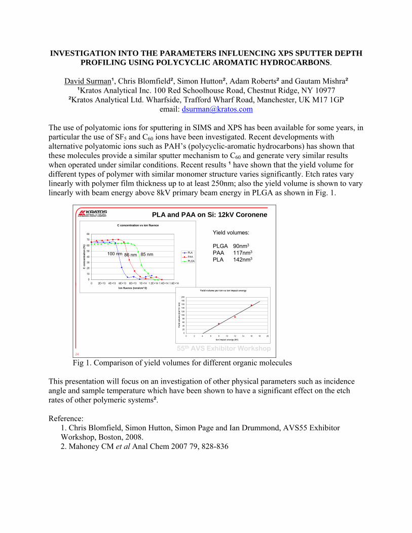
email: [email protected] The use of polyatomic ions for sputtering in SIMS and XPS has been available for some years, in particular the use of SF5 and C60 ions have been investigated. Recent developments with alternative polyatomic ions such as PAH’s (polycyclic-aromatic hydrocarbons) has shown that these molecules provide a similar sputter mechanism to C60 and generate very similar results when operated under similar conditions. Recent results ¹ have shown that the yield volume for different types of polymer with similar monomer structure varies significantly. Etch rates vary linearly with polymer film thickness up to at least 250nm; also the yield volume is shown to vary linearly with beam energy above 8kV primary beam energy in PLGA as shown in Fig. 1.
2455th AVS Exhibitor Workshop
PLA and PAA on Si: 12kV CoroneneC concentration vs ion fluence
0
10
20
30
40
50
60
70
80
0 2E+13 4E+13 6E+13 8E+13 1E+14 1.2E+14 1.4E+14 1.6E+14
Ion fluence (ions/cm^2)
C c
on
cen
trat
ion
(%
)
PLA
PAA
PLGA
85 nm86 nm100 nm
Yield volumes:
PLGA 90nm3
PAA 117nm3
PLA 142nm3
Yield volume per ion vs ion impact energy
0
20
40
60
80
100
120
140
160
180
200
0 2 4 6 8 10 12 14 16 18 20
Ion impact energy (kV)
Yie
ld v
olu
me
(nm
^3
/ io
n)
Fig 1. Comparison of yield volumes for different organic molecules This presentation will focus on an investigation of other physical parameters such as incidence angle and sample temperature which have been shown to have a significant effect on the etch rates of other polymeric systems². Reference:
1. Chris Blomfield, Simon Hutton, Simon Page and Ian Drummond, AVS55 Exhibitor Workshop, Boston, 2008. 2. Mahoney CM et al Anal Chem 2007 79, 828-836

FABRICATION OF PHOTO/BETA-VOLTAIC DIODES FROM BORON CARBIDE / SILICON HETEROJUNCTION
R. Bao1, J. Sandstrom2, S.R. Messenger4, S. Qadri4, A.N. Caruso2,3, and D.B. Chrisey1*
1Department of Materials Science and Engineering, Rensselaer Polytechnic Institute, Troy, NY,12180
2Center for Nanoscale Science and Engineering, North Dakota State University, Fargo, ND 58102
3Department of Physics, University of Missouri-Kansas City, Kansas City, MO 64110 4Naval Research Laboratory, Washington, DC 203755
email: [email protected] Tel: 518-698-2507 The long-lived and self-supplied beta-voltaic devices are very useful in remote and long term use, such as satellite in the aerospace, as well as conventional batteries in consumer devices, such as cell phones and laptop computers. But beta-voltaic devices made with conventional semiconductors tend to suffer very rapid degradation due to radiation damage. Fortunately, the degradation problem can potentially be alleviated by replacing conventional semiconductors with icosahedral boron carbide semiconductors, which have been proved to survive extensive irradiance due to the self-healing of icosahedral structure. In this poster, we report that the prototype photo/beta-voltaic diodes based on boron carbide/Si heterojunction have successfully fabricated. The results show that boron carbide thin film by PECVD has amorphous structure, and the remaining H in boron carbide thin film passivates the dangling bond and improves the voltaic performance of device. The quantum efficiency of boron carbide / Si diode is high in the range of 400 nm - 1000 nm, which indicates that boron carbide/Si diode is suitable to be used to make photovoltaic device. In both photo-voltaic and beta-voltaic characterization of boron carbide / Si diode, the repeatable response and sensitivity to the beam intensity were observed. Figure 1 The responses of B5C/Si heterojunction diode to irradiations under different intensity (a) the incident beam is fiber light (b) the incident beam is beta particles or electron beam with the energy of 120keV

TEST OF THE CONSISTENCY OF ANGLE RESOLVED XPS DATA FOR DEPTH
PROFILE RECONSTRUCTION USING THE MAXIMUM ENTROPY METHOD
C. Moffitt, A. Roberts, G. Mishra and K. Macak,
Kratos Analytical, Wharfside, Trafford Wharf Road, Manchester, M17 1GP, UK
Angle resolved XPS is a useful method for obtaining non-destructive quantification of thin (4-6nm) layers with good absolute depth resolution[1]. Although acquisition of ARXPS data with modern instrumentation is easy, determining the depth distribution of elements from the data is more challenging. The maximum entropy method (MEM) is a technique frequently used for solving the inversion problem in angle resolved XPS experiments. The MEMSYS algorithm used by Livesey and Smith[2] can provide an estimate of the optimum value of the regularizing parameter (smoothness), of the error bars in the reconstructed profile and of the noise level in the experimental data set. While for the artificial ARXPS datasets the interpretation of these factors is straightforward, the fitting of the experimental data may be complicated by the sample structure which does not always agree with the assumptions postulated by the model used in MEM calculations : the electron transport in the sample must be determined by the inelastic scattering with the constant mean free path throughout the sample and the material density must be constant throughout the sample. The necessary condition for the consistency of experimentally measured data with the MEM model (successful fit) is that the Laplace transform of the compositional depth profile (LTCDP) calculated from the experimentally measured normalized intensity is a monotonically decreasing function for all measured elements. We have found an efficient algorithm which can estimate the LTCDP for elements with different inelastic mean free paths and thus provide an independent estimate of the noise scaling calculated by the MEMSYS algorithm and verify whether the MEM model is appropriate for the measured data. Here we present results from a number of samples and draw conclusions on the use of these methods to generate elemental and chemical-state depth profiles. [1] P.J. Cumpson, J. Electron Specrosc. Rel. Phenom. 73 (1995) 25 [2] A. K. Livesey, G.C. Smith, J. of Elec. Spectroscopy 67 (1994) 439-961.

COMPLETE ANALYSIS OF MATERIALS USING COMPLEMENTARY TECHNIQUES
Vincent S. Smentkowski, Dave Wark, Laurie Le Tarte, Hong Piao, John C. Chera, Sara G.
Ostrowski and Akane Suzuki GE Global Research, Niskayuna, NY 12309
email: [email protected], phone 518-387-5467 A combination of complimentary analysis techniques has been used to characterize a diffusion couple sample. We will demonstrate that the results, when taken together, provide for a better understanding of the sample than the data from any one technique alone. The poster will summarize how diffusion couples are fabricated and highlight the benefits of each characterization technique. Electron Probe Micro Analysis (EPMA) provides for quantitative chemical analysis (spectrometry and imaging) of most elements (Z>4) at a concentration greater than about 0.1 % within a volume of 1-2 microns. EPMA also allows for imaging of both backscattered and secondary electrons. Auger Electron Spectroscopy (AES) has the smallest analytical spot, provides for quantitative analysis of all elements (except H and Li) present at concentrations of greater than about 0.5 atomic percent, and can perform high lateral resolution imaging. X-Ray Photoelectron Spectroscopy (XPS) provides for quantitative analysis of all elements (except H and Li) present at concentrations greater than about 0.5 atomic percent, is able to analyze insulating samples, and can provide information regarding the chemical state of the material. Time of Flight Secondary Ion Mass Spectrometry (ToF-SIMS) is able to detect all elements and high mass molecular fragment ions with high sensitivity, is able to analyze non-conductive samples, and the analyst does not need to select which species to analyze for prior to the measurement since a full mass spectrum is saved at every volume element. AES, XPS, and ToF-SIMS surface analysis instruments can operate in spectrometry modes (compositional analysis), imaging modes, as well as depth profiling modes (where one monitors the sample composition as a function of depth). In this poster, we will demonstrate that certain species reveal high ToF-SIMS spectral intensities even when present at low (ppm) concentrations.
SIMULATION STUDY OF TRANSMISSION ELECTRON MICROSCOPY IMAGING OF GRAPHENE STACKING
F. Nelson1, A.C. Diebold1, R. Hull2
1College of Nanoscale Science and Engineering, University at Albany, Albany, N.Y. 12203
2Rensselaer Polytechnic Institute (RPI), 110 8th St., Troy, NY 12180 email: [email protected]
Graphene's high mobility and mechanical integrity make it an attractive material for the “beyond CMOS” technology that will replace today’s transistor. Acceleration of process and device technology requires considerable advances in the imaging and characterization of graphene. The physical dimensions of available single and multi-layer samples are not large enough for many metrology methods. For example, the spot size of ellipsometry is typically larger than available samples. Electron microscopy of graphene is also challenging due to carbon's low atomic number. The high mobility of single layer and misoriented two and three layer graphene make it attractive for nanoelectronic devices. The current investigation explores HRTEM simulations of graphene stacking configurations AAA/ABA/ABC as well as bilayers with misorientations between the individual layers. Images calculated using the MacTempas program's multislice algorithm show discernable differences between the stacking sequences when simulated in the presence of random noise.

ADVANCED CHARACTERIZATION METHODS FOR SOLID OXIDE FUEL CELL MATERIALS
L.A. Le Tarte, J. Cournoyer, K. Dovidenko, J. Grande, E.J. Olson, J. A. Ruud, T. Striker
General Electric Global Research Center, K1 2C35, One Research Circle, Niskayuna, NY 12309 email: [email protected]
Lanthanum strontium manganite (LSM)/yttria stabilized zirconia (YSZ) and YSZ/Ni materials are currently under investigation for the cathode and anode layers in solid oxide fuel cell (SOFC) devices, respectively. Optimizing the performance of these materials requires engineering of the composite microstructures at the sub-micron scale. We have found that a combination of secondary electron (SE) imaging and Auger electron spectroscopy (AES) elemental mapping provides a good understanding of the porosity and phase distributions within these materials. Examination of the cathode and anode layer in SOFC device stacks requires cross sectioning. Traditional epoxy mounting and polishing is not an option for the combined SEM/AES characterizations. Epoxy is incompatible with the Auger UHV environment. This paper discusses two methods used to prepare SOFC device stacks. The first method is a modified transmission electron microscopy (TEM) sample preparation technique. This method is used for thin (<2mm), SOFC device stacks. The second method is to use focused ion beam (FIB) milling to generate the final polished region for the SEM/AES analysis. This technique has been used when the original sample is thicker than 2mm. The biggest advantage of FIB cross sectioning is its ability to produce smooth cut surfaces on non-homogeneous and porous materials. Another advantage is the precise positioning of the cuts with respect to the numerous interfaces in these complex stacks. The SE images and AES elemental maps can be used to determine the pore, LSM, and YSZ phase distributions within the cathode layer (Figure 1). Determining the microstructure and phase distributions within these layers following various process and test conditions allows optimization of the SOFC manufacturing process. Fig. 1a. SE image of a FIB prepared LSM/YSZ x-sec. Fig. 1b. Results of image analysis performed on Auger elemental maps.
1a 1b
Volume Porosity: 27% Zr phase: 38% La phase: 35%

LASER ABLATION-INDUCED ASSEMBLY AND SURFACE SINTERING OF NANOPARTICLES IN LIQUID
Zijie Yan, Ruqiang Bao, and Douglas B. Chrisey
Department of Materials Science and Engineering, Rensselaer Polytechnic Institute, Troy, NY 12180
email: [email protected], phone: 518-2539228
Laser ablation of target materials immersed in liquid environment is an easy method to fabricate nanoparticles, but the interaction of nanoparticles with laser beam during the ablation is very complex. Fragmentation of nanoparticles by laser reprocessing has been generally recognized, but a contrary process, the laser ablation-induced assembly, has been also observed in our experiments. Moreover, we have observed the surface laser sintering of the assembled nanoparticles by the laser heating and subsequent quenching in the liquid.
SPECTROSCOPIC ELLIPSOMETRY CHARACTERIZATION OF HIGH-K FILMS ON SiO2/Si
Ming Di,1 Eric Bersch,1 Steven Consiglio,2 Tianhao Zhang,1 Parul Tyagi,1 Robert D. Clark,2 Gert J. Leusink,2 Torsten Kaack,3 and Alain C. Diebold1
1 College of Nanoscale Science and Engineering (CNSE), University at Albany, 255 Fuller Rd., Albany, NY 12203
2 TEL Technology Center, America, LLC, 255 Fuller Rd. Albany, NY, 12203 3 KLA-Tencor Corp., One Technology Drive, Milpitas, CA 95035
With the shrinking of complementary metal oxide semiconductor (CMOS), traditional silicon dioxide based gate dielectrics are being replaced by high-k materials. For the 45 nm node and beyond, the requirements for the new gate dielectrics are high-k values for smaller equivalent oxide thickness (EOT), relative large band gaps for smaller gate leakage currents and compatibility with IC processes. Leading high-k material candidates include hafnium oxide, hafnium silicate and nitridated hafnium silicate films. A challenge with hafnium oxide based high-k materials is that they have high surface defect densities in contact with silicon compared to SiO2-Si interface. A SiO2 interfacial layer is necessary in between high-k dielectrics and silicon substrates. The thicknesses of both high-k layer and SiO2 interfacial layer are essential to device performance, the thickness measurements of these two layers are important to advance IC process control. Spectroscopic ellipsometry (SE) is a powerful metrology technique to measure the thicknesses of thin dielectrics materials with high precision. SE measures thicknesses of thin films by their optical properties, which are complex dielectric function or complex refractive index. The wavelength of traditional SE is from 240 nm to 800 nm. It is a challenge for SE to measure both high-k and SiO2 simultaneously, since the optical properties of both films are similar at wavelengths above 250 nm. However, the band gap of hafnium based high-k films is around 6 eV (λ=206nm). The band edge absorption of high-k films makes their optical dispersions different from those of SiO2. This mechanism is the theoretical basis for SE to measure both films simultaneously. Cody Lorentz model and Tauc Lorentz model are used to model the optical dispersions of amorphous high-k films. These models are used to differentiate the high-k films from SiO2 films in the modeling of the SE. In order to test these models, we designed an experiment by combining various HfO2 and SiO2 thicknesses for HfO2/SiO2/Si stacks. The thicknesses of high-k films were also measured by X-ray Reflectivity (XRR) and the thicknesses of the high-k and SiO2 films were measured by Angle Resolved X-ray photoemission Spectroscopy (ARXPS). Thickness results from all three of these methods will be presented and compared.

COMPARISON OF SAMPLE PREPARATION METHODS FOR ANALYSIS OF HYDRATED SAMPLES BY HIGH VACUUM TECHNIQUES
Sara G. Ostrowski; Lauraine Denault; Tracy L. Paxon; Vincent S. Smentkowski
General Electric Global Research Center, Niskayuna, NY, 12309 email: [email protected]
Imaging time of flight secondary ion mass spectrometry (ToF-SIMS) is touted as a label-free, high spatial resolution (<100 nm) technique for monitoring the distribution of molecules (native and exogenous) on biological samples. Proper sample preparation is critical to achieve meaningful results for analyses of biological (hydrated) samples under high vacuum. Using ToF-SIMS and scanning electron microscopy (SEM), this presentation will explore the degree of sample perturbation caused by different preparation methods, such as freeze-drying and critical point drying (CPD). The effect of freeze-drying on the chemical distribution and sample morphology is assessed using B-cells samples frozen in deep liquid nitrogen and freeze-dried in a Millrock Tech 24L freeze-drier. ToF-SIMS images show that the native chemical distribution of the B-cells was maintained on the micrometer-scale (Figure 1). Complementary SEM images demonstrate that cell morphology remained largely intact. Figure 1. ToF-SIMS images of Na (left) and phosphocholine (middle) and SEM image (right) for B-cells frozen in liquid nitrogen and freeze-dried. The influence of CPD on hydrated samples will also be explored using B-cells fixed in 2% glutaraldehyde, dehydrated in ethanol, and CPD. SEM images verify the presence of a large population of cells and demonstrate excellent morphology (Figure 2). Interestingly, phosphocholine signal is not detected by ToF-SIMS. It is likely that the ethanol treatment extracted the lipids from the cells, which may be a novel approach to circumvent the challenge of analyte signal suppression by lipid matrices.
Figure 2. ToF-SIMS images of Na (left) and phosphocholine (middle) and SEM image (right) for CPD B-cells.

TOUGHENING COPPER-SILICA INTERFACES BY METAL-CATALYZED MOLECULAR RING OPENING IN A NANOLAYER
Saurabh Garg1, Binay Singh1, Xinxing Liu2, P. G. Ganesan1, L. Interrante2, G. Ramanath1*
1Materials Science and Engineering Dept, Rensselaer Polytechnic Institute, Troy, NY 12180. 2Chemistry Department, Rensselaer Polytechnic Institute, Troy, NY 12180
The state-of-the-art nanodevice wiring requires near-zero-thickness interfacial barriers for inhibiting Cu transport into, and enhancing adhesion with, low dielectric permittivity (low k) materials. Currently used refractory metal-based barriers are not extendable for future devices due to difficulties in obtaining contiguous ultrathin layers in high aspect ratio features. The ultimate goal, however, is to eliminate the barrier and integrate Cu directly with the low-k dielectric such that there is high interfacial toughness without interfacial mixing. Low-k dielectrics derived from cyclolinear polycarbosilanes with 1,3-Disilacyclobutane (DSCB) rings offer promise for realizing this exciting possibility because Cu immobilization through strong ring opening and bonding could conceivably enhance adhesion as well as inhibit metal transport. Here, we demonstrate that introducing a molecular nanolayer of a DSCB-ring-terminated organosilane at copper-silica interfaces results in a 10-fold increase in fracture toughness upon annealing. Such chemically-induced interfacial toughening through interaction of copper with carbosilane rings confirms the possibility of, and paves the way for, realizing the direct integration of Cu with molecularly tailored low-k dielectric materials. We have also shown the surface cleaning of copper using DSCB rings, which reflects the thermal activated interaction between copper and ring. We synthesized DSCB ring-terminated organosilanes and assembled them on silica substrates to form a 0.7 nm thick molecular nanolayer, verified by variable take-off angle X-ray photoelectron spectroscopy (XPS) and ellipsometry. Four-point bending fracture tests on as-prepared Cu/DSCB/SiO2 sandwiches revealed a very low interface toughness of 2.1 J/m2, comparable to that exhibited by pristine Cu/SiO2 structures, consistent with core-level XPS spectra indicating Cu/DSCB interface fracture due to the lack of any significant bond formation. Upon annealing to 250 ºC fracture occurs at the DSCB/SiO2 interface, indicative of Cu-DSCB interface strengthening. The interfacial toughness increases monotonically with annealing temperature, yielding values as high as 21.3 J/m2 for Tanneal = 500 ºC. Interface strengthening is observed for annealing temperatures as low as 80 °C, suggesting that thermal activation is necessary for copper to interact with the DSCB rings. Interfaces with a methyl terminated monolayers (i.e., without the DSCB ring) showed 50% lower toughness values for the same deposition and annealing conditions, underscoring the crucial role of the DSCB rings. XPS fracture surface analysis combined with infrared analyses of the annealing behavior of DSCB-containing molecules on different surfaces shows that annealing-induced Cu-catalyzed ring opening of DSCB and strong siloxane bonding at the DSCB/SiO2 interface is the main mechanisms of interfacial toughening. Our results demonstrate that carbosilane rings could be useful to enhancing toughness of metal-dielectric interfaces either directly in a polymeric material or through use in a molecular nanolayer.

NITROGEN INCORPORATION IN SiO2/SIC INTERFACE
H. Piao1, J. Fronheiser1, K. Matocha1, Y. Hu2, A. Chatterjee3 1General Electric Co., Niskayuna, NY 12309, U.S.
2Canadian Light Source Inc., Saskatoon, SK. S7N 0X4, Canada 3General Electric Co, Bangalore 560066, India
email: [email protected] Silicon carbide (SiC) receives considerable attention for its potential use in high-power devices because of its ability to achieve high blocking voltage and operate at high temperature. The growth of high quality SiO2 on SiC is a crucial step to realize these applications. The nitridation of SiO2/SiC interfaces shows great promise as a means of achieving high quality gate oxides for SiC MOSFET structures. It is of critical importance to identify the nitrogen interfacial chemistry and understand the beneficial effects of nitridation treatment. In this work, the SiO2/SiC structure was obtained by direct oxidation in nitrous oxide (N2O), following a nitric oxide (NO) post-annealing. X-ray Photoelectron spectroscopy (XPS) in combination of dynamic Secondary Ion Mass Spectroscopy (SIMS) and synchrotron-based X-ray Absorption Near edge Structure (XANES) has been used to investigate the SiO2/SiC interface to determine the nitrogen concentrations and chemical bonding, therefore to understand the resulting improvements in electrical characteristics. The results show that nitridation introduces nitrogen into the SiO2/SiC interface to form silicon nitride (SiN bonds). Oxygen has also been incorporated into the oxynitride structure. A further study is necessary to elucidate the Si local bonding arrangements and to find out the possibility of nitrogen as dopant diffusion in the SiC.

THE DNA NANOPORE PROJECT
S.M. Rossnagel IBM T.J. Watson Research Center, Yorktown Heights, NY 10598.
email: [email protected] We have been developing a device based on a 2-3 nm diameter pore between two electrolyte volumes for the transit of DNA by means of a potential gradient. The nanopore is configured with 3 electrodes, each about 3 nm thick with dielectric spacers. The nanopore electrodes can be used to trap DNA in-transit, and ideally measure the impedance and hence the identity of each nucleotide as it passes through the nanopore, allowing real time sequencing of the DNA. The goal is to operate at megahertz, allowing sequencing of the entire genome within a few hours a fairly modest cost. This project has lead to numerous new developments in nanoscale fabrication, particularly for nanofluidics. This presentation. will focus on the nanofabrication as well as the new processes developed for working with materials, electrolytes, and junctions at this scale.