2005 ieee international solid-state circuits conference
TRANSCRIPT
ADVANCE PROGRAM
2005IEEE
INTERNATIONALSOLID-STATE
CIRCUITSCONFERENCE
FEBRUARY6, 7, 8, 9, 10
CONFERENCE THEME:
Entering the NanoelectronicIntegrated-Circuit Era
SAN FRANCISCOMARRIOTT HOTEL
IEE
E S
OL
ID-S
TAT
E C
IRC
UIT
S S
OC
IET
Y/IE
EE
SA
N F
RA
NC
ISC
O S
EC
TIO
N,B
AY
AR
EA
CO
UN
CIL
/UN
IV.O
F P
A.
SUND
AY A
LL-D
AY:2
FO
RUM
S:Hi
gh-F
requ
ency
Clo
ck G
ener
atio
n;Ad
vanc
ed D
RAM
;8 T
UTO
RIAL
S
3 SP
ECIA
L-TO
PIC
SESS
IONS
:Pow
erlin
e LA
N;Pr
oces
sor P
ower
Pro
blem
s;3D
Inte
grat
ion
THUR
SDAY
ALL
-DAY
:3 F
ORU
MS:
Imag
er C
hara
cter
izat
ion;
Nano
scal
e De
sign
;Aut
omot
ive
Circ
uits
;SHO
RT C
OUR
SE:R
F Ci
rcui
ts &
Sys
tem
s
5-DA
YPR
OGRA
M
2005AP_Pgs01_53v4.qxd 10/31/2004 2:31 PM Page 1
2
ISSCC VISION STATEMENT
The International Solid-State Circuits Conference is the foremost global forumfor the presentation of advances in solid-state circuits and systems-on-a-chip.The Conference offers a unique opportunity for engineers, working at the cut-ting edge of IC design and application, to maintain technical currency and tonetwork with leading experts.
CONFERENCE HIGHLIGHTS
On Sunday, February 6, the day before the official opening of the Conference,ISSCC 2005 offers:
• A choice of up to 3 of a total of 8 Tutorials• Two ISSCC Advanced Solid-State Circuit Design Forums:• GIRAFE (GHz Radio Front End) Advanced Solid-State Circuit
Design Forum: "Clock and Frequency Generation for Wireless and Wireline Applications"
• Memory Circuit Design Forum:“Advanced Dynamic-Memory Design”
The 90-minute tutorials offer background information and a review of the cur-rent state-of-the-art in specific circuit-design topics. In the all-day AdvancedSolid-State Circuit Design Forums, leading experts present state-of-the-artdesign strategies in a workshop-like format. The Forums are targeted atdesigners experienced in the technical field.
On Sunday evening, three Special-Topic Evening Sessions addressing next-generation circuit-design challenges will be offered, starting at 7:30PM:
• Powerline LAN• When Processors Hit the Power Wall• 3D System-on-Package• The Special-Topic Evening Sessions are open
to all ISSCC attendees.
On Monday, February 7, a record ISSCC technical program of 233 papers in 6parallel session, starts with 3 plenary talks: “Nanoelectronics for the UbiquitousInformation Society”; “Ambient Intelligence: Broad Dreams and NanoscaleRealities”; Innovation and Integration in the Nanoelectronics Era”. A SocialHour, open to all ISSCC attendees, will follow the afternoon session. The SocialHour will feature posters from the winners of the 2003-04 and 2004-05 jointDAC-ISSCC student-design contest. Monday evening features two panel dis-cussions and a Special-Topic Evening Session: Highlights of the Symposium onVLSI Technology, in which some of ISSCC-relevant papers from theSymposium are presented to intrigue and inspire ISSCC attendees.
On Tuesday, February 8, ISSCC 2005 offers morning and afternoon technicalsessions, followed by a Social Hour, a Special-Topic Evening Session onNanoscale SRAM and two panel discussions. Wednesday, February 9, fea-tures morning and afternoon technical sessions.
On Thursday, February 10, ISSCC 2005 offers a choice of four events:• An ISSCC Short Course: “RF Circuit Design from Technology to
Systems”. Two sessions of the Short Course will be offered,with staggered starting times.
• An ISSCC Advanced Solid-State-Circuit-Design Forum “Automotive Technology and Circuits”.
• An ISSCC Advanced Solid-State-Circuit-Design Forum onMicroprocessor Design: “Robust Design Solutions for NanoscaleCircuits: From DFM through End-of-Life”.
• An ISSCC Advanced Solid-State-Circuit-Design Forum:“Characterization of Solid-State Image Sensors”.
Registration for the Thursday events is limited. Registration will be filled on afirst-come first-served basis. Use of the ISSCC Web-registration site(www.isscc.org) is strongly encouraged. Web registrants will be provided withimmediate confirmation on registration for Tutorials, Advanced Solid-State-Circuit-Design Forums, and the Short Course.
2005AP_Pgs01_53v4.qxd 10/31/2004 2:31 PM Page 2
3
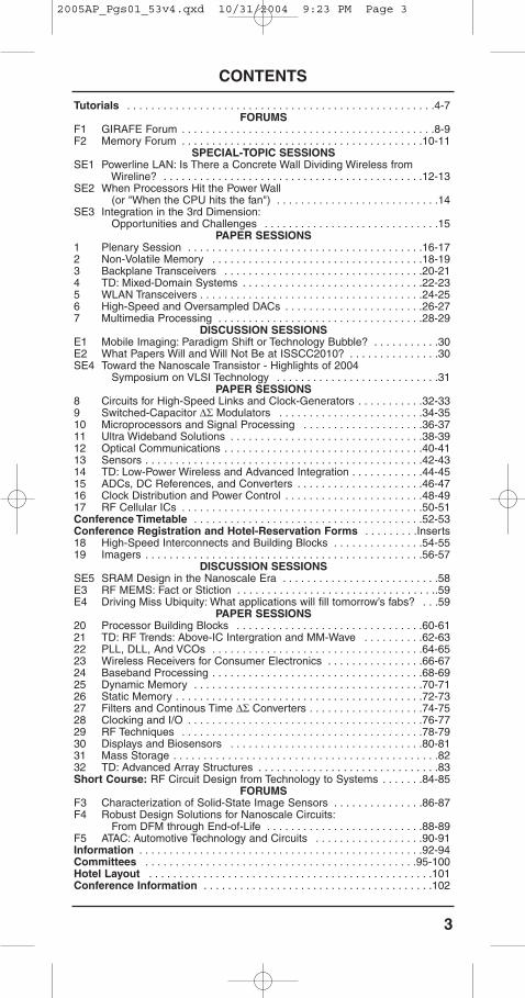
CONTENTS
Tutorials . . . . . . . . . . . . . . . . . . . . . . . . . . . . . . . . . . . . . . . . . . . . . . . . . . .4-7FORUMS
F1 GIRAFE Forum . . . . . . . . . . . . . . . . . . . . . . . . . . . . . . . . . . . . . . . . . .8-9F2 Memory Forum . . . . . . . . . . . . . . . . . . . . . . . . . . . . . . . . . . . . . . . .10-11
SPECIAL-TOPIC SESSIONS SE1 Powerline LAN: Is There a Concrete Wall Dividing Wireless from
Wireline? . . . . . . . . . . . . . . . . . . . . . . . . . . . . . . . . . . . . . . . . . . .12-13SE2 When Processors Hit the Power Wall
(or "When the CPU hits the fan") . . . . . . . . . . . . . . . . . . . . . . . . . . .14SE3 Integration in the 3rd Dimension:
Opportunities and Challenges . . . . . . . . . . . . . . . . . . . . . . . . . . . . .15PAPER SESSIONS
1 Plenary Session . . . . . . . . . . . . . . . . . . . . . . . . . . . . . . . . . . . . . . .16-172 Non-Volatile Memory . . . . . . . . . . . . . . . . . . . . . . . . . . . . . . . . . . .18-193 Backplane Transceivers . . . . . . . . . . . . . . . . . . . . . . . . . . . . . . . . .20-214 TD: Mixed-Domain Systems . . . . . . . . . . . . . . . . . . . . . . . . . . . . . .22-235 WLAN Transceivers . . . . . . . . . . . . . . . . . . . . . . . . . . . . . . . . . . . . .24-256 High-Speed and Oversampled DACs . . . . . . . . . . . . . . . . . . . . . . .26-277 Multimedia Processing . . . . . . . . . . . . . . . . . . . . . . . . . . . . . . . . . .28-29
DISCUSSION SESSIONSE1 Mobile Imaging: Paradigm Shift or Technology Bubble? . . . . . . . . . . .30E2 What Papers Will and Will Not Be at ISSCC2010? . . . . . . . . . . . . . . .30SE4 Toward the Nanoscale Transistor - Highlights of 2004
Symposium on VLSI Technology . . . . . . . . . . . . . . . . . . . . . . . . . . .31PAPER SESSIONS
8 Circuits for High-Speed Links and Clock-Generators . . . . . . . . . . .32-339 Switched-Capacitor ∆Σ Modulators . . . . . . . . . . . . . . . . . . . . . . . .34-3510 Microprocessors and Signal Processing . . . . . . . . . . . . . . . . . . . .36-3711 Ultra Wideband Solutions . . . . . . . . . . . . . . . . . . . . . . . . . . . . . . . .38-3912 Optical Communications . . . . . . . . . . . . . . . . . . . . . . . . . . . . . . . . .40-4113 Sensors . . . . . . . . . . . . . . . . . . . . . . . . . . . . . . . . . . . . . . . . . . . . . .42-4314 TD: Low-Power Wireless and Advanced Integration . . . . . . . . . . . .44-4515 ADCs, DC References, and Converters . . . . . . . . . . . . . . . . . . . . .46-4716 Clock Distribution and Power Control . . . . . . . . . . . . . . . . . . . . . . .48-4917 RF Cellular ICs . . . . . . . . . . . . . . . . . . . . . . . . . . . . . . . . . . . . . . . .50-51Conference Timetable . . . . . . . . . . . . . . . . . . . . . . . . . . . . . . . . . . . . . .52-53Conference Registration and Hotel-Reservation Forms . . . . . . . . .Inserts18 High-Speed Interconnects and Building Blocks . . . . . . . . . . . . . . .54-5519 Imagers . . . . . . . . . . . . . . . . . . . . . . . . . . . . . . . . . . . . . . . . . . . . . .56-57
DISCUSSION SESSIONSSE5 SRAM Design in the Nanoscale Era . . . . . . . . . . . . . . . . . . . . . . . . . .58E3 RF MEMS: Fact or Stiction . . . . . . . . . . . . . . . . . . . . . . . . . . . . . . . . ..59E4 Driving Miss Ubiquity: What applications will fill tomorrow’s fabs? . . .59
PAPER SESSIONS20 Processor Building Blocks . . . . . . . . . . . . . . . . . . . . . . . . . . . . . . .60-6121 TD: RF Trends: Above-IC Intergration and MM-Wave . . . . . . . . . .62-6322 PLL, DLL, And VCOs . . . . . . . . . . . . . . . . . . . . . . . . . . . . . . . . . . .64-6523 Wireless Receivers for Consumer Electronics . . . . . . . . . . . . . . . .66-6724 Baseband Processing . . . . . . . . . . . . . . . . . . . . . . . . . . . . . . . . . . .68-6925 Dynamic Memory . . . . . . . . . . . . . . . . . . . . . . . . . . . . . . . . . . . . . .70-7126 Static Memory . . . . . . . . . . . . . . . . . . . . . . . . . . . . . . . . . . . . . . . . .72-7327 Filters and Continous Time ∆Σ Converters . . . . . . . . . . . . . . . . . . .74-7528 Clocking and I/O . . . . . . . . . . . . . . . . . . . . . . . . . . . . . . . . . . . . . . .76-7729 RF Techniques . . . . . . . . . . . . . . . . . . . . . . . . . . . . . . . . . . . . . . . .78-7930 Displays and Biosensors . . . . . . . . . . . . . . . . . . . . . . . . . . . . . . . .80-8131 Mass Storage . . . . . . . . . . . . . . . . . . . . . . . . . . . . . . . . . . . . . . . . . . . .8232 TD: Advanced Array Structures . . . . . . . . . . . . . . . . . . . . . . . . . . . . . .83Short Course: RF Circuit Design from Technology to Systems . . . . . . .84-85
FORUMSF3 Characterization of Solid-State Image Sensors . . . . . . . . . . . . . . .86-87F4 Robust Design Solutions for Nanoscale Circuits:
From DFM through End-of-Life . . . . . . . . . . . . . . . . . . . . . . . . . .88-89F5 ATAC: Automotive Technology and Circuits . . . . . . . . . . . . . . . . . .90-91Information . . . . . . . . . . . . . . . . . . . . . . . . . . . . . . . . . . . . . . . . . . . . . . .92-94Committees . . . . . . . . . . . . . . . . . . . . . . . . . . . . . . . . . . . . . . . . . . . . .95-100Hotel Layout . . . . . . . . . . . . . . . . . . . . . . . . . . . . . . . . . . . . . . . . . . . . . . .101Conference Information . . . . . . . . . . . . . . . . . . . . . . . . . . . . . . . . . . . . . .102
2005AP_Pgs01_53v4.qxd 10/31/2004 9:23 PM Page 3
4
TUTORIALS
T1: INTEGRATED POWER MANAGEMENT
As circuit-design power requirements never align well with the availablepower source, power management along with efficiency and cost are crit-ical elements in all system designs. This tutorial provides an overview ofdc/dc converter techniques (switched-inductor, switched-capacitor, linear-regulator, and compound architectures), and offers a discussion of thepros and cons for each. The characteristics of today's portable powersources, lithium-ion batteries being the most common, are also discussed.Finally, the focus is on circuit techniques which may be integrated intoCMOS Systems-on-a-Chip when multiple supply voltages are required.
Instructor: Roy Kaller is Vice President of Engineering at SMSC inPhoenix, AZ where he is responsible for analog technology developmentand design automation. He joined SMSC as part of the company's acqui-sition of Gain Technology Corporation in June 2002. Prior to joining GainTechnology in 2000, he was the founder and director of NationalSemiconductor's Power Management design center in Grass Valley, CA.From 1992 until 1995, Roy was a design engineering manager for SiliconSystems, and he started his career at Burr-Brown Corporation in 1983where he developed a broad range of products including precision op-amps, MUXes, DACs, and ADCs. Roy has been a member of ISSCCAnalog Sub-committee since 2002, has published eight papers and holdsone patent in analog integrated circuits and solid state chemistry. Royearned his BSEE from the University of Arizona and is a graduate of theUniversity's Arizona Executive Program.
T2: INTRODUCTION TO I/O DESIGN FOR DIGITAL SYSTEMS
This tutorial gives an introduction to digital I/O circuit design. Topicsinclude essential transmission line theory, elements of transmitter andreceiver design (boundary-scan blocks, up/down converters, line driversand receivers, and ESD protection structures). In addition to moreadvanced topics such as differential I/O structures, on-chip termination,PVT compensation and clocking for I/O interfaces are discussed.
Instructor: Thucydides Xanthopoulos received his BS, MS, and PhD inElectrical Engineering and Computer Science from the MassachusettsInstitute of Technology in 1992, 1995, and 1999, respectively. From 1999to 2001 he was a consulting engineer with the Alpha Development Group,Compaq Computer in Shrewsbury, MA, where he designed the clock-gen-eration and distribution network for the Alpha 21364 server processor(EV7). Since 2001, he has been a principal member of Technical Staff withCavium Networks in Marlboro, MA, where he co-leads silicon implemen-tation of security and network services processors and is primarily respon-sible for I/O, clocking, power distribution, and package design.
2005AP_Pgs01_53v4.qxd 10/31/2004 2:31 PM Page 4
5
Sunday, February 6th 8:00 AM
T3: RF MEMS: Devices, Circuits and Packaging
RF MEMS devices including micromechanical switches, resonators, 3Dhigh-Q inductors and micromachined antennas can enable ultra-low-power wireless architectures in ultra-small microsystems. High-Q micro-mechanical resonators in the VHF and UHF range have become available,and wafer-level-packaged MEMS switches have demonstrated reliableoperation for billions of cycles. This tutorial presents an introduction to RFMEMS devices, reviews the latest advances in the field, and discussestheir manufacturing, performance and packaging.
Instructor: Farrokh Ayazi is an Assistant Professor in the School of ECEat Georgia Tech. He received his BSEE from the University of Tehran, in1994, and MSEE and PhD degrees from the University of Michigan, in1997 and 2000, respectively. His research interests are in the areas ofmicro-/nano-electromechanical resonators, RF MEMS, VLSI Analog IC's,MEMS inertial sensors and packaging. He is a 2004 recipient of the NSFCAREER Award, the 2004 Richard M. Bass Outstanding Teacher Award,and the Georgia Tech College of Engineering Cutting Edge ResearchAward for 2001-2002. He has served on the technical program committeesof the IEEE ISSCC, MEMS, and Sensors conferences.
T4: PHASE-CHANGE MEMORY
Phase-change memory (PCM, also called OUM or PRAM), is an emerg-ing non-volatile-memory technology that has the potential to improve theperformance compared to Flash - write throughput (versus NOR), randomread access time and throughput (versus NAND, direct write, bit granular-ity, endurance) - and to be scalable beyond Flash. The basic concepts ofPCM, the memory cells, the electrical characteristics and the scaling per-spective are reviewed. Key design aspects and challenges, related to theMOS-selected cell array as well as to the BJT-selected array, includingexamples and published results, are discussed.
Instructor: Giulio Casagrande graduated in Electronic Engineering in1977 at the University of Padova, Italy. He joined ST Microelectronics,Milano, as a designer of EPROMs and EEPROMs and then he led thedesign and engineering team that developed the first generations of Flashmemories in ST. He is presently Director of R&D of the Memory ProductsGroup at ST Microelectronics, concentrating on advanced Flash designsolutions for embedded applications, assessment and disruptive emergingmemories, CAD and design methodology. He is a member of ISSCCMemory Sub-Committee.
2005AP_Pgs01_53v4.qxd 10/31/2004 2:31 PM Page 5
6
TUTORIALS
T5: DSP CIRCUIT TECHNOLOGIES FOR THE NANOSCALE ERA
Some of the sub-65nm scaling challenges and new paradigm shifts innext-generation DSP architectures are discussed. Emerging trends inwireless and embedded DSP industry including special-purpose multime-dia/communication accelerators, co-processor arrays, and reconfigurableDSP engines are reviewed. Energy-efficient arithmetic and logic circuittechniques, static/dynamic supply scaling, and multi-supply/multi-thresh-old design for switching and leakage energy reduction are described.Dedicated hardware accelerators and data-path building blocks forenabling high MOPS/W in specialized DSP tasks are presented. Manychip design examples and their results/trade-offs are be shown as part ofthis tutorial.
Instructor: Ram Krishnamurthy is a Senior Staff Research Engineer atIntel Corporation's Circuit Research Laboratories in Hillsboro, OR, wherehe leads the high-performance and low-voltage circuits research group. Heholds 41 patents issued and published over 75 papers. He serves on theSRC ICSS task force and the ISSCC, CICC, and SoC program commit-tees. Since 1999 he serves as an adjunct faculty member at Oregon StateUniversity, where he teaches VLSI system design. He received his PhDfrom Carnegie Mellon University in 1998
T6: NANOTECHNOLOGY 101
This tutorial provides the attendee with an introduction to the emergingopportunities in novel nanoscale devices and fabrication techniques withparticular emphasis on the implications for circuit and system designers.Topics covered include: fundamentals of device physics and materials sci-ence at the nanoscale, the ITRS emerging research devices (memory &logic), nanotubes, nanowires, and nanoparticles, molecular devices, andnanofabrication techniques and their impact on device layout. An assess-ment of the level of maturity for the proposed devices will be given.
Instructor: H.-S. Philip Wong joined the IBM T. J. Watson ResearchCenter, Yorktown Heights, NY, in 1988. While at IBM Research, he was aSenior Manager having the responsibility of shaping and executing IBM'sstrategy on nanoscale science and technology and semiconductor tech-nology. In September, 2004, he joined Stanford University as a Professorof Electrical Engineering.
2005AP_Pgs01_53v4.qxd 10/31/2004 2:31 PM Page 6
7
Sunday, February 6th 8:00 AM
T7: POLAR MODULATORS FOR LINEAR WIRELESS TRANSMITTERS
As spectral efficiency becomes increasingly important, most emergingwireless standards apply both amplitude and phase modulation and therefore require linear modulators. Polar modulators can produce morespectrally pure signals with higher power efficiency than traditional linearmodulators. This tutorial provides an introduction to the concept of polarmodulation and an in-depth look at some of the implementation challenges. The following topics are covered at both system and circuitlevels:(1) An overview of linear wireless transmitters (2) Polar modulator implementation, including impairment mechanisms
and limitations are detailed.(3) Case studies of practical modulators for EDGE are treated
Instructor: Antonio Montalvo has been the director of Analog DevicesDesign Center in Raleigh, NC, since 2000. He is also an Adjunct Professorat North Carolina State University. He was with Ericsson from 1995 to2000 where he led the RF IC group and with Advanced Micro Devices from1987 to 1991 where he was involved with the design of Flash memories.He received a PhD from North Carolina State University in 1995, an MSEEfrom Columbia University in 1987 and a BS Physics from Loyola Universityin 1985.
T8: HIGH-SPEED ELECTRICAL INTERFACES:STANDARDS AND CIRCUITS
The physical-level standard specification space (including standards underdevelopment) and challenges in multi-gigabit range high-speed electricalinterfaces area, such as XFI, CEI , XAUI, Fiber-Channel, SAS, SATA, etc.are reviewed. Jitter requirements, signal amplitude, impedance, S-param-eter specifications and transmission channel representation, along withequalization techniques, are studied. Block diagrams and circuit solutionsare also discussed. This tutorial helps to understand IC design parame-ters, their link to standard specifications, and current and future challengesin wireline design for multi-gigabit electrical interfaces.
Instructor: Yuriy M. Greshishchev, is a Technical Advisor on high-speed circuit design for wireline communications at PMC Sierra,Ottawa, Canada,. His design experience is in multi-gigabit rate CMOS,SiGe, III-V circuits for telecommunications and data communicationsapplications area. He has been involved in XFI, fiber channel , SAS, RIOphysical level standard technical groups. Yuriy is a member of ISSCCTechnical Program Committee for five consecutive years. He presented anISSCC Tutorial on "Front-end Circuit Design for Optical Communications"in 2001. He has co-authored two books and numerous technical papers onthe area of high-speed communication circuit design and data converters.He received his PhD degree in Electrical and Computer Engineering fromV.M. Glushkov Institute of Cybernetics, Microelectronics Division, Kiev,Ukraine, in 1984.
2005AP_Pgs01_53v4.qxd 10/31/2004 2:31 PM Page 7
8
GIRAFE FORUM
F1 Clock and Frequency Generation for Wireline and Wireless Apllications
(Salon 9)
Organizer: Rudolf Koch, Infineon, Munich, Germany
Committee: Franz Dielacher, Infineon, Villach, AustriaTrudy Stetzler, Texas Instruments, Stafford, TXCharles Chien, SST Communications,
Santa Monica, CAJohn Long, Delft University of Technology,
Delft, The NetherlandsRoger Minear, Agere Systems, Wyomissing, PATakehiko Nakao, Toshiba, Kanagawa, JapanTom Schiltz, Linear Technology,
Colorado Springs, CO
The quality of the spectrum of clock generators has a crucial impact on theperformance of communications systems. Different system concepts mayyield widely disparate specifications for VCOs and PLLs even for the sameapplication.
Trade-offs between contradictory requirements, such as low phase noise and wide bandwidth, are needed to fulfill and optimize system specifications.
The morning sessions of this forum deal with fundamental aspects of frequency generation. The first two speakers treat design criteria for clockgeneration for wireless and wireline systems. The modeling of noisesources in oscillator circuits is addressed by the next three presenters.
In the afternoon sessions, each of the three speakers discusses analysisand design of PLL frequency synthesizers, fractional-N frequency synthesizers, and spread-spectrum PLLs for communication applications.
Finally, at the end of the afternoon, the speakers will assemble in a panelformat to field questions and comments from the audience.
2005AP_Pgs01_53v4.qxd 10/31/2004 2:31 PM Page 8
9
Sunday, February 6th 8:00 AM
Forum Agenda:
Time Topic
8:00 Continental Breakfast
8:30 Welcome and IntroductionRudolf Koch, Infineon, Munich, Germany
08:35 Formulating Design Criteria for Frequency Generation for Wireless Applications
Derek Shaeffer, Aspendos Communications, San Jose, CA
09:05 Formulating Design Criteria for Clock Generation for Wireline Applications
Takehiko Nakao, Toshiba, Kanagawa, Japan
09:35 Multiphase Ring Oscillators and Oscillator Phase Noise Modelling Techniques
Robert Renninger, Agere, Allentown, PA
10:05 Break
10:35 VCO Design and Phase Noise ModellingAli Hajimiri, California Institute
of Technology, Pasadena, CA
11:35 Supply and Substrate Noise in VCOsJan Craninckx, IMEC, Leuven, Belgium
12:05 Lunch
1:30 System Analysis, Simulation, Design and Optimization of PLL Frequency Synthesizers for Communication Systems
Cicero Vaucher, Philips, Eindhoven, The Netherlands
2:30 Design, Simulation, and Bandwidth Extension Methods for Fractional-N Frequency Synthesis
Michael Perrott, Massachsetts Institute of Technology, Cambridge, MA
3:30 Break
4:00 Spread Spectrum PLLs;Direct Modulation with Wideband PLLs
Ivan Bietti, STMicroelectronics, Pavia, Italy
5:00 Panel Discussion
5:30 Conclusion
2005AP_Pgs01_53v4.qxd 10/31/2004 2:31 PM Page 9
10
MEMORY FORUM
F2: Advanced Dynamic Memory Design
(Salon 7)
Organizer/Chair: Katsuyuki Sato, Elpida., Tokyo, JapanCommittee: Jinyong Chung, POSTECH, Pohang, Korea
Young-Hyun Jun, Samsung, HwaSung, KoreaTerry Lee, Micron Technology, Boise, IDJohn Barth, IBM, Essex Junction, VTMartin Brox, Infineon, Munich, GermanyTakayuki Kawahara, Hitachi, Tokyo, Japan
DRAM is widely used not only as the main memory in PCs and servers,but also as the active memory in consumer products such as digital cam-eras, TVs, and mobile phones. Consequently, cost reduction is a para-mount design consideration. Each new generation of DRAM has appliedfiner-pattern technology to cut costs. In this sense, new DRAM designsare leading-edge- technology-driven. This forum informs the audienceabout current DRAM technology and its associated circuit issues.
Jinyong Chung provides an overview of DRAM architecture, from basiccell operation to a chronological evolution of cell configuration. Cell leak-age, soft errors related to alpha and neutron particles, and bit-line couplingare treated. Test-time-reduction methods to screen defective cells aredescribed, and redundancy techniques to replace defective cells, rows orcolumns are developed. Size and voltage issues associated with furtherscaling are also discussed.
High-speed DRAM architecture and design is the focus of the second talkby Young-Hyun Jun. The key to high-speed operation is the internal clock-generation process in which DLLs and PLLs are vital. From basic circuitconcepts to current practice, DLL and PLL design issues are discussed.The application of DLL and PLL techniques in graphics RAM and DDR2are among the products illustrated. The new technologies needed to real-ize future high-speed DRAMs are presented.
The DRAM I/O interface is the subject of the talk by Terry Lee. Cost min-imization, test-time reduction, the test of multiple devices in parallel, low-power multi-drop busses and upgradability are among the critical featuresneeded in DRAM applications. This causes DRAM I/O to differ from datacommunications and backplane signaling. The theme of this presentationis the circuit and system design issues related to high-speed DRAM inter-faces.
On-chip SRAM cache density is restricted by the limitations in SRAM size.High-performance embedded DRAM is aimed at applications employingon-chip cache. John Barth describes the technology of embedded DRAMto realize high speed and a wide internal bus with a minimum die penaltywhile suppressing noise. Structures for high-speed embedded DRAMtesting are described, and design-for-test techniques are introduced.
Martin Brox focuses on DRAM for mobile applications including browsers,cameras, and video-conferencing. These all require high-density DRAMs.The talk treats the design of mobile RAM to meet the unique requirementsnecessitated by such applications.
2005AP_Pgs01_53v4.qxd 10/31/2004 2:31 PM Page 10
11
Sunday, February 6th 8:00 AM
Takayuki Kawahara introduces the design of sub-1V DRAMs which playcritical roles in reducing dissipation in MPU/SoC/SiP for power-aware systems. However, four major challenges need be faced to achieve this:reducing leakage currents; maintaining the signal charge of memory cells;reducing speed variations caused by deviations of threshold voltage, and reducing the cell size. He presents current advances to dealwith these issues in sub-1V DRAMs, and solutions for nanoscale LSI system.
Tomoyuki Ishii introduces future challenges for DRAM technology in the nanoscale process generation. From an operational-stability point-of-view,DRAM has better scalability than SRAM. However, the standard 1T1Ctype DRAM has serious difficulties in maintaining adequate retention timeand storage capacitance, as the process scales. Several non-1T1Capproaches for scalable DRAM are introduced, along with new devicestructures. Investigation of a memory cell using only 10 electrons per bitis discussed.
Forum Agenda:
Time Topics
8:00 Continental Breakfast
8:30 Introduction & UpdatesJinyong Chung, POSTECH, Pohang, Korea
9:15 High-Speed DRAM DesignYoung-Hyun Jun, Samsung, HwaSung, Korea
10:15 Break
10:30 DRAM I/O InterfaceTerry Lee, Micron Technology, Boise, ID
11:30 High Performance Embedded DRAM and test structuresJohn Barth, IBM, Essex Junction, VT
12:30 Lunch
1:15 DRAM Design for Mobile ApplicationsMartin Brox, Infineon, Munich, Germany
2:15 Sub-1V DRAM DesignTakayuki Kawahara, Hitachi, Tokyo, Japan
3:15 Break
3:30 DRAM in Nanoscale EraTomoyuki Ishii, Hitachi, Tokyo, Japan
4:30 Conclusion
2005AP_Pgs01_53v4.qxd 10/31/2004 2:31 PM Page 11
12
SE1: Powerline LAN: Is There a Concrete Wall Dividing Wirelessfrom Wireline?
(Salon 8)
Organizer: Mark Ingels, STMicroelectronics Zaventem, Belgium
Chair: Michael Green, University of California, Irvine, CA
From offices to coffee houses, wireless LANs have become ubiquitouswithin the United States. However, there are many situations where a wire-less signal encounters attenuation within a building. For example concretewalls and ceilings are known to impede RF transmission. In such situationsPower Line Communication (PLC) is emerging as an alternative technolo-gy for high-speed data communication within the home. This new technol-ogy can assist or even replace the wireless systems as needed. In thisSpecial-Topic Evening session, the significance of PLC will be revealed.Infrastructural aspects that may affect the choice between wireline andwireless for the transmission of broadband data is addressed and theadvantages and needs for powerline systems is demonstrated. The ses-sion gives an overview and comparison of various available and emergingPLC technologies and practical systems are presented.
SPECIAL-TOPIC EVENING SESSIONS
2005AP_Pgs01_53v4.qxd 10/31/2004 2:31 PM Page 12
13
Sunday, February 6th 7:30 PM
SE1: Powerline LAN: Is There a Concrete Wall Dividing Wirelessfrom Wireline?
Time Topics
7:30 Broadband Powerline Multimedia Home Networking:Advantages and Challenges,
Haniph A. Latchman, University of FloridaGainesville, FL
8:00 OFDM for Powerline CommunicationsJim Petranovich, Conexant Systems,
San Diego, CA
8:30 Performance Analysis of a CDMA Chipset for InHouseBroadband Powerline Communications,
Vincent Buchoux, LEA, Courbevoie, France
9:00 Remote Control via Powerline,Claudio Cantoro, Dora, Milano, Italy
2005AP_Pgs01_53v4.qxd 10/31/2004 2:31 PM Page 13
14
SE2: When Processors Hit the Power Wall (or "When the CPU hits the fan").
(Salon 7)
Organizer: Sam Naffziger, Hewlett Packard, Fort Collins, CO CO - Organizer: James Warnock, IBM, Yorktown Heights, NYCO - Organizer: Herbert Knapp, Infineon, Munich, Germany
Power consumption and heat removal have become first-order limiters to"Moore's Law" in regards to the growth of processor performance. Thislimitation has bubbled up from mobile devices to desktop systems and noweven server processors are investing heavily in techniques that manageand reduce power consumption. The result is a fundamental shift in howcircuit designers and architects attempt to achieve performance from eachnew design generation. No aspect of the processor design ecosystemgoes untouched: silicon process technology, circuit design, computerarchitecture, packaging and cooling are all facing fundamental shifts in pri-orities and methods. The power consumption problem on leading edgeprocessors and the possible technology directions in architecture, circuitsand cooling are explored in this special-topics session. The first step tosolving a problem is to understand it better by identifying it. So we beginby examing where the power is consumed on a leading edge processorand how it varies with time and workload. The next talk involves a look atone of the frontiers of VLSI design: the many opportunities present in cre-ating "environmentally aware" chips that measure and react to their envi-ronment to optimize power, performance and other tradeoffs. Lastly two ofthe industries leading architects discuss the meaning of "low-power archi-tecture", and some of the brightest opportunities for power efficiency. Thesession concludes with a look by one of the leading innovators in coolingtechnology at how waste heat that byproduct of computation can beremoved efficiently.
Time Topic
7:30 pm Spatially Resolved Imaging Of Microprocessor PowerHendrik Hamann, IBM, Yorktown Heights, NY
8:00 pm Adaptive Techniques for Managing Power Consumption
Takayasu Sakurai, University of Tokyo, Tokyo, Japan
8:30 pm Low-Power for High-Performance PC Compatible Processors
David R. Ditzel, Transmeta Corporation,Santa Clara, CA
9:00 pm Power-Efficient Stream ArchitecturesWilliam Dally, Stanford University
and Stream Processors, Palo Alto, CA
9:30 pm Advanced Cooling for High Performance VLSIKen Goodson, Stanford University, Palo Alto, CA
SPECIAL-TOPIC EVENING SESSIONS
2005AP_Pgs01_53v4.qxd 10/31/2004 2:31 PM Page 14
15
Sunday, February 6th 7:30 PM
SE3: Integration in the 3rd Dimension:Opportunities and Challenges
(Salon 9)
Organizer: Larry Pileggi, Carnegie Mellon University, Pittsburgh, PA Chair: Werner Weber, Infineon, Munich, Germany
While it is apparent that integrating electronic systems beyond two dimen-sions can potentially provide great advantages, it is less obvious what themost promising approaches for such integration will be with future tech-nologies. The papers in this session will describe and evaluate variousopportunities and challenges for vertical integration of integrated electron-ic systems. Cost considerations are considered prominently, as well as thepotential performance improvements that are realized. Various integrationconcepts are considered for integrated systems which include digital logic,analog circuits and sensors. The session begins with a cost-based argu-ment for 2.5D integration based on stacking of traditional 2D integrated cir-cuits. Results indicate a performance advantage as well due to the short-ening of long interconnect wiring when integrating in 3D. A subsequentpaper applies similar performance reasoning for "folding" ICs into multipleactive layers to reduce the lateral dimensions. Exciting opportunities arefurther explored for expanding in the 3rd dimension via RF-MEMS com-ponents that are built directly on top of monolithic ICs. Then, the sessioncloses with a description of how wafer-scale integration in the third dimen-sion is used to construct antennas and other microwave components thatwould otherwise be challenging, if not impossible, for traditional monolith-ic design.
Time Topic
7:30 Exploring Cost and Performance Advantages of 2.5-D Integration
Wojciech Maly, Carnegie Mellon University,Pittsburgh, PA
8:00 3D Integration's Architectural and Circuit Design Opportunities
Wilfried Haensch, IBM, Yorktown Heights NY
8:30 Above IC & embedded RF MEMs platform for SoC Integration: Status and Prospect
Pascal Ancey, STMicroelectronics, Crolles Cedex, France
9:00 A Wafer Level Integration Technology for On-WaferAntennas and Microwave Components
Hermann Schumacher, University of Ulm,Ulm, Germany
2005AP_Pgs01_53v4.qxd 10/31/2004 2:31 PM Page 15
16
PLENARY SESSION - INVITED PAPERS
Chair: Timothy Tredwell, Eastman Kodak, Rochester, NYISSCC Executive-Committee Chair
Associate Chair: Ian Young, Intel, Hillsboro, ORISSCC Program-Committee Chair
FORMAL OPENING OF THE CONFERENCE 8:30AM
1.1 Nanoelectronics for the Ubiquitous Information Society
8:40AM
Daeje Chin, Minister of Information and Communications,Korea
Nanoelectronics will open up both new opportunities and new challenges.Meanwhile, it has been successfully used in mass production of gigabitmemories, including Flash and DRAM, and in field-emission display (FED)with carbon nano-tubes. The technical challenge is to deal with processand device parameter variation, while the economic challenge is to reducethe high cost of fabrication. One way to overcome these technical and eco-nomic uncertainties is to organize a tight collaboration of the device indus-try with system and service industries, to distribute the risk, and to maxi-mize the total social benefit. The “IT 839 Strategy” of the KoreanGovernment is an example of such a program to enhance cooperationamongst service, system, and device industries, to speed up the use ofnanoelectronics for the realization of a ubiquitous information society. Insuch a society, information technology (IT) enables everyone to enjoy dailylife without awareness of IT itself. This is made possible by the "InvisibleSilicon" that resides within almost everything in our society, to sense, ana-lyze, and control ourselves and our environment. Nanoelectronics allowsthe mass production of such new silicon. RFID chips and sensor networksare examples of "Invisible Silicon", which will integrate nano-electro-mechanical systems and RF technology, as well as low-power and multi-media SoCs. These technologies will facilitate future IT, and change ourworld, just as fourth-generation mobile-phone developments are leadingus to the ubiquitous information society.
ISSCC, SSCS, JSSCC, & IEEE AWARD PRESENTATIONS9:30AM
BREAK 10:00 AM
1.2 Ambient Intelligence: Broad Dreams and Nanoscale Realities
10:15AM
Hugo De Man, Senior Research Fellow, IMEC;Professor, Katholieke Universiteit Leuven, Belgium
Ambient Intelligence (AmI) is a vision of a world in which people will besurrounded by networks of intelligent devices that are sensitive to, andadaptive to, their needs. This concept implies a consumer-oriented indus-try driven by software from the top, and enabled (and constrained) bynano-scale physics at the atomic level. "more-Moore" will be needed todeliver the Giga-ops computation and GHz communication capabilitiesrequired for stationary and wearable devices. But AmI also creates newchallenges at the architectural and physical levels. To make Aml possible,AmI devices need two-orders-of-magnitude-lower power dissipation than
SESSION 1 SALON 7-9
2005AP_Pgs01_53v4.qxd 10/31/2004 2:31 PM Page 16
17
Monday, February 7th 8:30 AM
today's microprocessors, at one-twentieth of the cost. But these require-ments conflict with the embedded programmability needed for personal-ization and adaptation to new services. We will focus on emerging tech-niques for bridging this gap between software-centric systems and power-efficient platform architectures for AmI devices.
A second challenge is to cope with the fact that nano-scale physical phe-nomena are in conflict with the traditional "nice and predictable" digitalabstractions now used for complexity management. Techniques for copingwith uncertainty and signal degradation, while achieving better-than-worst-case design, will be discussed.
Finally, one must realize that to facilitate AmI, "more-than-Moore" tech-nology is required, for example, for the design of autonomous wirelesssensor networks. Correspondingly, attention will be paid to novel combi-nations of technologies above and around CMOS, for the design of ultra-low-power, ultra-simple sensor motes for AmI.
1.3 Innovation and Integration in the Nanoelectronics Era11:05AM
Sunlin Chou, Senior Vice President and General Manager, Technology and Manufacturing Group,Intel, Hillsboro, OR
Demand for electronics continues to grow as new products combine andenhance computing, communications, and digital capabilities. Hardwareand software are evolving to enable new applications and usage modes,by offering features such as multitasking, parallel processing, mobility andwireless connectivity. Integration at both component and product platformlevels, and efficient use of power, will become more important. These callfor holistic solutions involving systems, circuits, processes, devices, andpackaging. Many techniques to improve power efficiency have beendeveloped and more will emerge. Silicon technology and scaling remainkeys to progress, with transistors and circuit elements already atnanoscale dimensions. Innovation will accelerate as nanotechnology further renews and extends silicon technology. Skillful integration of newmaterials, processes, and device structures will be essential. Successfulnanoelectronics companies will excel in innovation and integration, extendMoore's Law into and beyond the next decade, and drive the developmentof future growth opportunities.
2005AP_Pgs01_53v4.qxd 10/31/2004 2:31 PM Page 17
18
SESSION 2 SALON 1-6
NON-VOLATILE MEMORY
Chair: Yair Sofer, Saifun Semiconductors, Netanya, IsraelAssociate Chair: Yukihito Oowaki, Toshiba, Kawasaki, Japan
2.1 A 146mm2 8Gb NAND Flash Memory in 70nm CMOS 1:30 PM
T. Hara1, K. Fukuda1, K. Kanazawa1, N. Shibata1, K. Hosono1, H. Maejima1,M. Nakagawa1, T. Abe1, M. Kojima1, M. Fujiu1, Y. Takeuchi1, K. Amemiya1, M. Morooka1, T. Kamei2, H. Nasu2, K. Kawano2, C-M. Wang3, K. Sakurai1, N. Tokiwa1, H. Waki1, T. Maruyama1, S. Yoshikawa1, M. Higashitani3, T. Pham3
1Toshiba, Yokohama, Japan2SanDisk, Yokohama, Japan3SanDisk, Sunnyvale, CA
A 146mm2 8Gb NAND flash memory with 4-level programmed cells is fabricated in a 70nm CMOS technology. A single-sided pad architectureand extended block-addressing scheme without redundancy is adoptedfor die size reduction. The programming throughput is 6MB/s and is comparable to binary flash memories.
2.2 An 8Gb Multi-Level NAND Flash Memory in a 63nm CMOS Process
2:00 PMD-S. Byeon, S-S. Lee, Y-H. Lim, J-S. Park, W-K. Han, P-S. Kwak, D-H. Kim, D-H. Chae, S-H. Moon, S-J. Lee, H-C. Cho, J-W. Lee, J-S. Yang, Y-W. Park, D-W. Bae, J-D. Choi, S-H. Hur, K-D. SuhSamsung, Hwasung, Korea
An 8Gb multi-level NAND flash memory is fabricated in a 63nm CMOStechnology with shallow trench isolation. The cell and chip sizes are0.02µm2 and 133mm2, respectively. Performance improves to 4.4MB/s byusing the 2x program mode and by decreasing the cycle time from 50nsto 30ns. This also improves the read throughput to 23MB/s.
2.3 Enhanced Write Performance of a 64Mb Phase-Change RAM2:30 PM
H-R. Oh, S. KANG, B. Cho, W. Cho, B-G. Choi, H. Kim, K-S. Kim, D-E. Kim, C-K. Kwak, H-G. ByunSamsung, Hwasung, Korea
A 1.8V 64Mb Phase-Change RAM with improved write performance is fab-ricated in a 0.12µm CMOS technology. The improvement of RESET andSET distributions is based on cell current regulation and multiple step-down pulse generators. The read access time and SET-write time are68ns and 180ns, respectively.
BREAK 3:00 PM
2005AP_Pgs01_53v4.qxd 10/31/2004 2:31 PM Page 18
19
Monday, February 7th 1:30 PM
2.4 A 128Mb NOR Flash Memory with 3MB/s Program Time andLow-Power Write Using an In-Package Inductor Charge-Pump
3:15 PMR. Sundaram, J. Javanifard, P. Walimbe, B. Pathak, R. Melcher, P. Wang, J. TacataIntel, Folsom, CA
Improved performance of flash memories requires programming morecells in parallel. This design uses an inductive pump to transfer the energy to a capacitor to achieve the needed voltage. The discrete inductor is bonded atop the die which also includes the control circuitry.With an inductive pump, the current saving in the program mode is 47.5mA compared to a capacitive pump.
2.5 A 125MHz Burst-Mode Flexible Read-While-Write 256Mb NOR Flash Memory
3:45 PMC. Villa1, D. Vimercati1, S. Schippers1, E. Confalonieri1, M. Sforzin1, S. Polizzi2, M. La Placa2, C. Lisi1, A. Magnavacca1, E. Bolandrina1, A. Martinelli1, V. Dima1, A. Scavuzzo2, B. Calandrino2, N. Del Gatto1, M. Scardaci3, F. Mastroianni1, M. Pisasale3, A. Geraci1, M. Gaibotti1, M. Sali11STMicroelectronics, Agrate Brianza, Italy2STMicroelectronics, Palermo, Italy3STMicroelectronics, Catania, Italy
A 1.8V 256Mb 2b/cell NOR flash memory is designed in a 130nm technology. A fast gate-voltage-ramp constant-current-reading concept isimplemented to obtain a robust read-while-write/erase function and125MHz burst read frequency.
2.6 A 90nm 512Mb 166MHz Multi-Level Cell Flash with 1.5MB/sProgramming
4:15 PMM. Taub1, R. Bains1, H. Castro1, S. Eilert1, R. Fackenthal1, C. Haid1, K. Parat2, S. Peterson1, A. Proescholdt1, K. Ramamurthi1, P. Ruby1, M. Szwarc1, D. Young1
1Intel, Foslom, CA2Intel, Santa Clara, CA
A 2b/cell flash memory in 90nm triple-well CMOS technology achieves1.5MB/s programming and 166MHz synchronous operation. The designfeatures 2-row programming, optimized program control hardware, 3 transistor x-decoder with negative deselected rows and configurableoutput buffers. The die is 42.5mm2 with a cell size of 0.076µm2.
2.7 126mm2 4Gb Multi-Level AG-AND Flash Memory with 10MB/s Programming Throughput
4:45 PMH. Kurata2, Y. Sasago2, K. Otsuga2, T. Arigane2, T. Kawamura2, T. Kobayashi2, H. Kume3, K. Homma3, K. Kozakai3, S. Noda3, T. Ito3, M. Shimizu3, Y. Ikeda3, O. Tsuchiya3, K. Furusawa3
1Hitachi, Kokubunji, Japan2Hitachi, Tokyo, Japan3Renesas Technology, Tokyo, Japan
A 4Gb flash memory, fabricated in 90nm CMOS technology, results in a126mm2 chip size and a 0.0162µm2/b cell size. Address and temperaturecompensation methods control the resistance of the inversion-layer localbit-line. Programming throughput of 10MB/s is achieved by using self-boosted charge injection scheme.
CONCLUSION 5:15 PM
2005AP_Pgs01_53v4.qxd 10/31/2004 2:31 PM Page 19
20
SESSION 3 SALON 7
BACKPLANE TRANSCEIVERS
Chair: Mehmet Soyuer, IBM, Yorktown Heights, NYAssociate Chair: Muneo Fukaishi, NEC, Kanagawa, Japan
3.1 A 5Gb/s NRZ Transceiver with Adaptive Equalization for Backplane Transmission
1:30 PMN. Krishnapura, M. Barazande-Pour, Q. Choudhry, J. Khoury, K. Lakshimikumar, A. AggarwalVitesse Semiconductor, Somerset, NJ
The proposed 5Gb/s transceiver has a transmitter with 2-tap pre-empha-sis and an adaptive receiver with 1-tap feedforward and 3-tap decisionfeedback equalization. The quad transceiver occupies 12mm2 in 0.13µmCMOS, consumes 2.1W from 1.2V, and has a BER <10-15 over 4 pairs of1-meter backplane trace with crosstalk.
3.2 A 6.4Gb/s CMOS SerDes Core with Feedforward and Decision-Feedback Equalization
2:00 PMM. Sorna1, T. Beukema2, K. Selander1, S. Zier1, B. Ji1, P. Murfet3, J. Mason3, W. Rhee2, H. Ainspan2, B. Parker2
1IBM, Hopewell Junction, NY2IBM, Yorktown Heights, NY3IBM, Hursley, United Kingdom
A 4.9 to 6.4Gb/s 2-level SerDes ASIC I/O core designed in 0.13µm CMOSuses a 4-tap FFE in the transmitter and a 5-tap DFE with receiver AGC.Error-free operation is achieved on channels with over 30dB loss at thehalf-baud rate. The TX/RX pair consumes 290mW from a 1.2V supply anduses a die area of 0.79mm2.
3.3 A 0.6 to 9.6Gb/s Binary Backplane Transceiver Core in 0.13µm CMOS
2:30 PMK. Krishna1, D. Yokoyama-Martin1, S. Wolfer1, C. Jones2, M. Loikkanen1,J. Parker1, R. Segelken1, J. Sonntag1, J. Stonick1, S. Titus3, D. Weinlader1
1Synopsys, Hillsboro, OR2Stexar, Hillsboro, OR3UNC, Chapel Hill, NC
A backplane transceiver core in 0.13µm dual-gate CMOS, operating at 0.6to 9.6Gb/s with an area of 0.56mm2 and dissipating 150mW at 6.25Gb/s,is presented. This core uses a unique adaptive receive equalization strategy, transmit pre-emphasis, and has extensive optional test featuresincluding a built-in BER tester and an on-chip receiver sampling scope.
BREAK 3:00PM
2005AP_Pgs01_53v4.qxd 10/31/2004 2:31 PM Page 20
21
Monday, February 7th 1:30 PM
3.4 A Transmit Architecture with 4-Tap Feedforward Equalizationfor 6.25/12.5Gb/s Serial Backplane Communications
3:15 PMP. Landman, K. Brouse, V. Gupta, S. Wu, R. Payne, U. Erdogan, R. Gu, A-L. Yee, B. Parthasarathy, S. Ramaswamy, B. Bhakta, W. Mohammed, J. Powers, Y. Xie, L. Wu, L. Dyson, K. Heragu, W. LeeTexas Instruments, Dallas, TX
A transmit architecture with a programmable 4-tap feedforward equalizerfor 6.25 to 12.5Gb/s serial communications through lossy channels isdescribed. A 16:8-channel MUX/DEMUX chip fabricated in a 0.13µm 7MCMOS process, demonstrates a near-end jitter or 16ps and an equalizedfar-end jitter of 55ps at 6.25Gb/s over a 36'' legacy backplane channel.
3.5 A 6.25Gb/s Binary Adaptive DFE with First Post-Cursor TapCancellation for Serial Backplane Communications
3:45 PMR. Payne, B. Bhakta, S. Ramaswamy, S. Wu, J. Powers, B. Parthasarathy,P. Landman, U. Erdogan, A-L. Yee, R. Gu, L. Wu, Y. Xie, K. Brouse, W. Mohammed, K. Heragu, V. Gupta, L. Dyson, W. LeeTexas Instruments, Dallas, TX
A 6.25Gb/s serial receiver with a 4-tap adaptive DFE is implemented in a0.13µm 7LM CMOS process. Direct cancellation of the first post-cursorISI is achieved, enabling recovery of a data eye fully closed from channellosses and crosstalk. A BER<10-15 is measured over legacy backplanechannels.
3.6 12Gb/s Duobinary Signaling with x2 Oversampled Edge Equalization
4:15 PMK. Yamaguchi1, K. Sunaga1, S. Kaeriyama1, T. Nedachi1, M. Takamiya1,K. Nose1, Y. Nakagawa1, M. Sugawara2, M. Fukaishi11NEC, Sagamihara, Japan2NEC, Santa Clara, CA
A backplane transceiver in 90nm CMOS that employs duobinary signalingover copper traces is described. To introduce duobinary signaling intodata transfers on printed boards, three techniques are developed: 1) edgeequalization for equalizer adaptation, 2) 2x oversampled transmitter equalizer for ISI control, and 3) 2b-transition-ensure encoding for clockrecovery.
3.7 A 25Gb/s PAM4 Transmitter in 90nm CMOS SOI4:45 PM
C. Menolfi1, T. Toifl1, R. Reutemann2, M. Ruegg2, P. Buchmann1, M. Kossel1, T. Morf1, M. Schmatz1IBM, Rueschlikon, Switzerland2Miromico, Zurich, Switzerland
A 25Gb/s multi-level PAM4 transmitter intended for short-range chip-to-chip on-board interconnects is presented. A 4-tap FIR pre-emphasis fil-tering scheme is used to equalize channel loss and to improve eye open-ing. Fabricated in a low-k partially depleted 90nm SOI technology, it occu-pies 0.052mm2 and draws 99.3mA from a 1V supply.
CONCLUSION 5:15 PM
2005AP_Pgs01_53v4.qxd 10/31/2004 2:31 PM Page 21
22
SESSION 4 SALON 8
TD: MIXED-DOMAIN SYSTEMS
Chair: Kerry Bernstein, IBM, Essex Junction, VTAssociate Chair: Siva Narendra, Intel, Hillsboro, OR
4.1 Joining Ionics and Electronics: Semiconductor Chips with Ion Channels, Nerve Cells and Brain Tissue
1:30 PMP. FromherzMax Planck Institute for Biochemistry, Munich, Germany
The microscopic interfacing of semiconductor devices and living neuronalsystems is discussed. From the biological side, ion channels, nerve cells,and brain tissue are considered. Basic experimental studies are performedwith capacitors and transistors of simple silicon chips. The approach isextended to a CMOS chip with 16000 transistor sensors.
4.2 An Analog Bionic Ear Processor with Zero-Crossing Detection
2:00 PMR. Sarpeshkar, M. Baker, C. Salthouse, J-J. Sit, L. Turicchia, S. ZhakMassachusetts Institute of Technology, Cambridge, MA
A 75dB 251µW analog speech processor is described that preserves theperformance, robustness, and programmability needed for deaf patients ata reduced power consumption compared to that of implementations withA/D and DSP. It also provides zero-crossing outputs for stimulation strate-gies that use phase information to improve performance.
4.3 An IC/Microfluidic Hybrid Microsystem for 2D Magnetic Manipulation of Individual Biological Cells
2:30 PMH. Lee1, Y. Liu1, E. Alsberg2, D. Ingber2, R. Westervelt1, D. Ham1
1Harvard University, Cambridge, MA2Harvard Medical School, Boston, MA
A microfluidic system is fabricated on top of an IC chip, suspending mag-netic-bead-tagged biological cells in a biocompatible environment. The ICproduces patterned magnetic fields using a microcoil array to manipulateindividual bead-bound cells. The hybrid prototype manipulates bovine cap-illary endothelial cells with precise spatial control.
BREAK 3:00 PM
4.4 A VLSI Analog Computer/Math Co-Processor For A Digital Computer
3:15 PMG. Cowan, R. Melville, Y. TsividisColumbia University, New York, NY
A single-chip VLSI analog computer having 80 integrators and 336 otherprogrammable linear and nonlinear circuits is fabricated in a 0.25µmCMOS process. The chip can be used to accelerate a digital computer'snumerical routines. The IC is 1cm2 and consumes 300mW.
2005AP_Pgs01_53v4.qxd 10/31/2004 2:31 PM Page 22
23
Monday, February 7th 1:30 PM
4.5 Towards Chip-Scale Atomic Clocks3:45 PM
C. Nguyen1, J. Kitching2
1DARPA, Arlington, VA, and University of Michigan, Ann Arbor, MI2NIST, Boulder, CO
MEMS technology is used to shrink atomic clocks from their present-daytable-top sizes down to only 1cm3 while at the same time retaining timingstability on the order of 30ns over one hour. The power consumption of thesystem is less than 30mW.
4.6 Opportunities for Optics in Integrated Circuits Applications4:15 PM
D. Miller, A. Bhatnagar, S. Palermo, A. Emami-Neyestanak, M. HorowitzStanford University, Stanford, CA
Optics potentially addresses two key problem in electronic chips and sys-tems: interconnects and timing. Short optical pulses (e.g., picoseconds orshorter) offer particularly precise timing. Results are shown for optical andelectrical four-phase clocking, with <1ps rms jitter for the optical case.
4.7 Processing of MEMS Gyroscopes on Top of CMOS ICs4:45 PM
A. Witvrouw1, A. Mehta1, A. Verbist1, B. Du Bois1, S. Van Aerde2, J. Ramos-Martos3, J. Ceballos3, A. Ragel3, J. Mora3, M. Lagos3, A. Arias3, J. Hinojosa3,J. Spengler4, C. Leinenbach5, T. Fuchs5, S. Kronmueller5
1IMEC, Leuven, Belgium2ASM, Leuven, Belgium3IMSE-CNM, Sevilla, Spain4Philips Research, Boeblingen, Germany5Bosch, Gerlingen-Schillerhoehe, Germany
Integrated 10µm thick poly-SiGe gyroscopes are processed on top of an8” standard 0.35µm CMOS wafer with 5 metal levels by using an advancedplasma-enhanced chemical vapor deposition multi-layer technology. Thegyroscopes are free-moving with Q-factors for the drive mode up to 10000at the pressure of 0.8mTorr while the CMOS chip is fully functional.
CONCLUSION 5:15 PM
2005AP_Pgs01_53v4.qxd 10/31/2004 2:31 PM Page 23
24
SESSION 5 SALON 9WLAN TRANSCEIVERS
Chair: Arya Behzad, Broadcom, San Diego, CAAssociate Chair: Mototsugu Hamada, Toshiba, Kawasaki, Japan
5.1 An Auto-I/Q Calibrated CMOS Transceiver for 802.11g1:30 PM
Y. Hsieh1, W-Y. Hu2, S-M. Lin2, C-L. Chen2, W-K. Li2, S-J. Chen1, D. Chen3
1National Taiwan University, Hsin-Chu, Taiwan2Muchip, Hsin-Chu, Taiwan3National Taiwan University, Taipei, Taiwan
The CMOS transceiver IC uses the super-heterodyne architecture toimplement a 802.11g RF front-end with auto I/Q calibration function.1° quadrature mismatch and 0.1dB gain mismatch can be achieved afterthe auto tuning in both the transmitter and receiver sides. Implemented ina 0.25µm CMOS process with 2.7V supply, the transceiver achieves a5.1dB receive cascade NF and a 7dBm transmit output P1dB.
5.2 An 802.11g WLAN SoC2:00 PM
S. Mehta1, D. Weber1, M. Terrovitis1, K. Onodera1, M. Mack1, B. Kaczynski1,H. Samavati1, S. Jen1, W. Si1, M. Lee1, K. Singh1, S. Mendis1, P. Husted1, N. Zhang1, B. McFarland1, D. Su1, T. Meng2, B. Wooley2
1Atheros Communications, Sunnyvale, CA2Stanford University, Stanford, CA
A single-chip 802.11g-compliant WLAN radio that implements all RF, analog, and digital PHY and MAC functions is implemented in a 0.18µmCMOS technology. The IC transmits 4dBm EVM-compliant output powerfor a 64QAM OFDM signal. The overall receiver sensitivities are -95dBmand -73dBm for data rates of 6Mb/s and 54Mb/s, respectively.
5.3 A Fully Integrated SoC for 802.11b in 0.18µm CMOS2:30 PM
H. Darabi, S. Khorram, Z. Zhou, T. Li, B. Marholev, J. Chiu, J. Castaneda,E. Chien, S. Anand, S. Wu, M. Pan, H. Kim, P. Littieri, B. Ibrahim, J. Rael,L. Tran, E. Geronaga, J. Trachewsky, A. RofougaranBroadcom, Irvine, CA
A 0.18µm CMOS 802.11b SoC integrated all the radio building blocksincluding the PA, the PLL loop filter, and the antenna switch, as well as thecomplete physical layer and the MAC sections. At 2.4GHz, it dissipates165mW in the receive-mode and 360mW in the transmit-mode from a 1.8Vsupply. The receiver achieves a typical NF of 6dB, and –88dBm sensitivityat 11Mb/s rate. The transmitter delivers a nominal output power of 13dBm.
BREAK 3:00 PM
5.4 A Compact Dual-Band Direct-Conversion CMOS Transceiver for 802.11a/b/g WLAN
3:15 PMZ. Xu1, S. Jiang1, Y. Wu1, H-Y. Jian1, G. Chu1, K. Ku1, P. Wang1, N. Tran1,Q. Gu1, M-Z. Lai1, C. Chien1, M. Chang1,2, P. Chow1
1SST Communications, Santa Monica, CA2University of California, Los Angeles, CA
A dual-band direct-conversion RF transceiver for 802.11a/b/g WLAN isimplemented in 0.18µm CMOS technology with 6mm2 die size and 182mWpower dissipation while transmitting 1dBm at 5GHz. The receiver achieves5dB NF, -8dBm IIP3 (high LNA gain), 96dB total gain, and -31.4dB EVM.The transmitter achieves 1dBm and 2.5dBm linear output power at 5GHzand 2.4GHz, respectively, with an EVM less than -31dB.
2005AP_Pgs01_53v4.qxd 10/31/2004 2:31 PM Page 24
25
Monday, February 7th 1:30 PM
5.5 A Low-Power Dual-band Triple-Mode WLAN CMOS Transceiver
3:45 PMT. Maeda, T. Yamase, T. Tokairin, S. Hori, R. Walkington, K. Numata, N. Matsuno, K. Yanagisawa, N. Yoshida, H. Yano, Y. Takahashi, H. HidaSNEC, Tsukuba, Japan
The 0.18µm CMOS direct-conversion dual-band triple-mode WLAN transceiver covers 2.4 to 2.5GHz and 4.9 to 5.95GHz and draws 78mA inthe receive mode and 76mA in the transmit mode, from a 1.8V supply bothat 2.4/5GHz. The system NF of 3.5/4.2dB, the sensitivity of -93/-94dBm for a 6Mb/s OFDM signal, and the EVM of 3.2/3.4% areobtained at 2.4/5.2GHz.
5.6 An SoC for Bidirectional Point-to-Multipoint Wireless Digital Audio Applications
4:15 PMK. Kianush1, J. Rapp2, D. Westberg2, J. van Valburg3, P. Johansson2,R. Ponnette4, N. Philips4
1Catena, Delft, The Netherlands2Catena, Kista, Sweden3Catena, Eindhoven, The Netherlands4Philips, Leuven, Belgium
A single-chip transceiver for wireless digital audio applications is realizedin a 0.25µm BiCMOS process. To avoid the congested 2.4GHz band andto achieve better penetration through walls, 863 and 915MHz bands areadopted. The frame structure used in this design guarantees a low laten-cy for streaming audio. Adaptive frequency hopping and antenna diversityensure robust link management.
5.7 A Dual-Band Frequency Synthesizer for 802.11a/b/g with Fractional-Spur Averaging Technique
4:45 PMS. Pellerano, S. Levantino, C. Samori, A. LacaitaPolitecnico di Milano, Milan, Italy
A 0.25µm BiCMOS spur-compensated fractional-N PLL is implemented inan 802.11a/b/g zero-IF transceiver. The synthesizer covers the 2.4 to2.5GHz and the 5.1 to 5.9GHz bands with 0.5MHz and 5MHz resolution,respectively. The phase noise integrated from 10kHz to 10MHz is lowerthan 1.25° rms for any synthesized carrier. The power consumption is39/59mW in 2.5/5GHz mode from 2.5V supply.
5.8 A Fully Integrated Transformer-Based Front-End Architecture for Wireless Transceivers
5:00 PMI. Bhatti, R. Roufoogaran, J. CastanedaBroadcom, Irvine, CA
A fully integrated transformer-based RF front-end architecture is present-ed that integrates matching, combining, and T/R switch functions on chip.The front-end is implemented in a 0.18µm CMOS Bluetooth transcieverachieving -90dBm receiver sensitivity and 2dBm transmit power from a1.8V supply.
CONCLUSION 5:15 PM
2005AP_Pgs01_53v4.qxd 10/31/2004 2:31 PM Page 25
26
SESSION 6 SALON 10-15
HIGH-SPEED AND OVERSAMPLED DACs
Chair: Robert Neff, Agilent Technologies, Palo Alto, CAAssociate Chair: Zhongyuan Chang, IDT-Newave Technology,
Shanghai, China
6.1 A 1.2GS/s 15b DAC for Precision Signal Generation1:30 PM
R. Jewett, J. Liu, K. PoultonAgilent Technologies, Palo Alto, CA
A 1.2GS/s 15b DAC achieves untrimmed SFDR of -70dBc to fs/4 and -63dBc to Nyquist (with 10dB better results at 500MS/s). A per-elementresampling scheme and dynamic element matching achieve DNL of2LSBs. In RZ output mode, ACPR for a 20MHz band at 900MHz is 69dB.The chip uses 40GHz-fT NPNs and is implemented in 0.35µm CMOS.
6.2 A 1.6GS/s 12b RTZ GaAs RF DAC for Multiple Nyquist Operation
2:00 PMM-J. Choe, K-H. Baek, M. TeshomeRockwell, Thousand Oaks, CA
RZ current switches are added to a current steering DAC for high-fre-quency wideband applications to achieve 800MHz bandwidth at 1st and 2nd
Nyquist band without the need for a reverse sinc equalization filter.Implemented in a GaAs HBT process with 4.5µm2 minimum emitter area,the DAC dissipates 1.2W at -5V with a 1.6GHz clock and 0dBm typical output power.
6.3 A 1.7GHz 3V Direct Digital Frequency Synthesizer with an On-chip DAC in 0.35µm SiGe BiCMOS
2:30 PMK-H. Baek, E. Merlo, M-J. Choe, A. Yen, M. SahrlingRockwell, Thousand Oaks, CA
A single-chip direct digital frequency synthesizer with hardware efficientphase-to-amplitude mapping and an integrated DAC achieves over 50dBSFDR in full-Nyquist band at 1.7GHz clock frequency for synthesized out-put signals up to 850MHz. The IC is implemented in a 0.35µm SiGeBiCMOS process and occupies an area of 4.8×5.0mm2. Power efficiencyis 1.76mW/MHz at 3V.
BREAK 3:00 PM
6.4 A 12b 500MS/s DAC with >70dB SFDR up to 120MHz in 0.18µm CMOS
3:15 PMK. Doris1,2, J. Briaire1, D. Leenaerts1, M. Vertregt1, A. van Roermund2
1Philips, Eindhoven, The Netherlands2Technical University Eindhoven, Eindhoven, The Netherlands
A CMOS current steering 12b 500MS/s 216mW DAC without any additional circuitry to remove errors introduced during the conversionprocess has >70dB SFDR up to 120MHz above the Nyquist band. This iscomparable to state-of-the-art performance requiring additional circuitry,and better than any design without additional circuitry.
2005AP_Pgs01_53v4.qxd 10/31/2004 2:31 PM Page 26
27
Monday, February 7th 1:30 PM
6.5 A 350MHz Low-OSR ∆Σ Current-Steering DAC with Active Termination in 0.13µm CMOS
3:45 PMM. Clara, W. Klatzer, A. Wiesbauer, D. StraeussniggInfineon, Villach, Austria
A time-interleaved architecture overcomes the dynamic performance limi-tations of standard DWA switching. Clocked at 350MHz, the DAC withactive output buffer achieves a linearity of 76dB for a signal swing of1.536V and an effective resolution of 11.9b in a bandwidth of 29.16MHz.It is fabricated in a standard 0.13µm CMOS process and consumes 62mWfrom a 1.5V supply.
6.6 Integrated Stereo ∆Σ Class D Amplifier4:15 PM
E. Gaalaas1, B. Liu2, N. Nishimura2
1Analog Devices, Bedford, MA2Analog Devices, Tokyo, Japan
A 2×40W (into 4Ω with a 20V supply) integrated stereo ∆Σ class D ampli-fier with 100dB SNR is realized in a 0.6µm CMOS process with DMOStransistors and buried zener diodes. Feedback from power stage outputsgives 0.001% THD and 65dB PSRR. The modulator clock rate is 6MHz,but dynamically adjusted quantizer hysteresis reduces the output data rateto 450kHz, helping achieve 88% efficiency.
6.7 A 22GS/s 6b DAC with Integrated Digital Ramp Generator4:45 PM
P. Schvan1, D. Pollex1, T. Bellingrath2
1Nortel Networks, Ottawa, Canada2Institut fuer Mikroelektronik Stuttgart, Germany
A 22GS/s 6b DAC is presented that includes a digital ramp pattern gener-ator. The DAC core and ramp generator consume 2W and 1.2W respec-tively operating from 3.3V. The DAC produces a differential signal up to1.3Vpp. DNL<0.5LSB and INL<0.9LSB are measured. The highest glitchenergy is 0.5pVs. Settling times are 70 and 40ps for full- and half-scaletransitions, respectively.
6.8 A 2GHz Mean-Square Power Detector with Integrated Offset Chopper
5:00 PMM. Kouwenhoven, A. van StaverenNational Semiconductor, Delft, The Netherlands
A 2GHz mean-square power detector with integrated chopper is present-ed. It typically achieves an offset reduction of 14.8dB compared to un-chopped, untrimmed units and 12dB reduction of the offset variation overtemperature (-40°C to +85°C) compared to laser-trimmed units. The chipis designed in a 0.35µm BiCMOS process, measures 1.5x1.5mm2 anddraws 8mA from a 2.7V supply.
CONCLUSION 5:15 PM
2005AP_Pgs01_53v4.qxd 10/31/2004 2:31 PM Page 27
28
SESSION 7 NOB HILL
MULTIMEDIA PROCESSING
Chair: Lee-Sup Kim, KAIST, Daejeon, KoreaAssociate Chair: Masafumi Takahashi, Toshiba, Kawasaki, Japan
7.1 A 1.3TOPS H.264/AVC Single-Chip Encoder for HDTV Applications
1:30 PMY-W. Huang1, T-C. Chen1, C-H. Tsai1, C-Y. Chen1, T-W. Chen1, C-S. Chen2,C-F. Shen3, S-Y. Ma3, T-C. Wang4, B-Y. Hsieh5, H-C. Fang1, L-G. Chen1
1National Taiwan University, Taipei, Taiwan2Chip Implementation Center, Hsin-Chu, Taiwan3Vivotek, Taipei, Taiwan4Chin Fong Machine Industrial, Chang Hua, Taiwan5MediaTek, Hsin-Chu, Taiwan
An H.264/AVC encoder is implemented on a 31.72mm2 die with 0.18µmCMOS technology. A four-stage macroblock pipelined architectureencodes 720p 30f/s HDTV videos in real time at 108MHz. The encodedvideo quality is competitive with reference software requiring 3.6TOPS ona general-purpose processor-based platform.
7.2 An 81MHz 1280x720Pixelsx30f/s MPEG-4 Video/Audio CODEC Processor
2:00 PMH. Yamauchi, S. Okada, M. Suzuki, Y. Matsuo, Y. Ishii, T. Mori,T. Watanabe, Y. MatsushitaSanyo Electric, Gifu, Japan
A high-definition MPEG-4 CODEC processor capable of encoding 720pimages (1280x720 pixels 30f/s) at 81MHz is presented. The CODEC isimplemented with only 390k gates and an 80kb SRAM. It is fabricated in a0.13µm CMOS process on a 5.6mmx5.6mm die.
7.3 An H.264/MPEG-4 Audio/Visual CODEC LSI with Module-Wise Dynamic Voltage/Frequency Scaling
2:30 PMT. Fujiyoshi, S. Shiratake, S. Nomura, T. Nishikawa, Y. Kitasho, H. Arakida, Y. Okuda, Y. Tsuboi, M. Hamada, H. Hara, T. Fujita, F. Hatori, T. Shimazawa, K. Yahagi, H. Takeda, M. Murakata, F. Minami, N. Kawabe, T. Kitahara, K. Seta, M. Takahashi, Y. OowakiToshiba, Kawasaki, Japan
A single-chip H.264/MPEG-4 audio/visual LSI for mobile applications witha module-wise dynamic voltage/frequency scaling architecture isdescribed. This LSI operates even during the voltage/frequency transitionwith no performance overhead by using a dynamic de-skewing system andan on-chip voltage regulator with slew-rate control. The IC consumes90mW in decoding QVGA H.264 video at 15f/s and MPEG-4 AAC LCaudio simultaneously.
BREAK 3:00 PM
2005AP_Pgs01_53v4.qxd 10/31/2004 2:31 PM Page 28
29
Monday, February 7th 1:30 PM
7.4 A Streaming Processing Unit for a CELL Processor3:15 PM
B. Flachs1, S. Asano2, S. Dhong1, P. Hofstee1, G. Gervais1, R. Kim1, T. Le1,P. Liu1, J. Leenstra3, J. Liberty
1, B. Michael, S. Mueller3, O. Takahashi1,
Y. Watanabe2, A. Hatakeyama4, H. Oh1, N. Yano2
1IBM, Austin, TX2Toshiba, Austin, TX3IBM, Boeblingen, Germany4Sony, Austin, TX
The design of a 4-way SIMD streaming data processor emphasizesachievable performance in area and power. Software controls data movement and instruction flow, and improves data bandwidth and pipelineutilization. The micro-architecture minimizes instruction latency and provides fine-grain clock control to reduce power.
7.5 A 600MIPS 120mW 70µA Leakage Triple-CPU MobileApplication Processor Chip
3:45 PMS. Torii1, S. Suzuki2, H. Tomonaga1, T. Tokue2, J. Sakai1, N. Suzuki1,K. Murakami2, T. Hiraga2, K. Shigemoto2, Y. Tatebe2, E. Obuchi2, N. Kayama2, M. Edahiro1, T. Kusano2, N. Nishi11NEC, Sagamihara, Japan2NEC, Kawasaki, Japan
A triple-CPU mobile application processor is developed on an8.95mmx8.95mm die in a 0.13µm CMOS process. The IC integrates3xARM926 cores, a DSP, several accelerators, as well as strong bus andmemory interfaces. It consumes 120mW for digital TV, web browser, and3D graphics, and 250mW@200MHz for 600MIPS with full processing.
7.6 90nm Low-Leakage SoC Design Techniques for Wireless Applications
4:15 PMP. RoyannezTexas Instruments, Villeneuve Loubet, France
The new generation of multimedia-application processors requires a dras-tic leakage reduction to bring the standby current to 50µA. An efficient setof leakage reduction techniques, including power gating, memory reten-tion, voltage scaling, and dual Vt, is employed on a 50M transistor, 80mm2
IC, fabricated in a 90nm CMOS technology, resulting in a 40x leakagereduction.
7.7 A 100-Channel Analog CMOS Auditory Filter Bank for Speech Recognition
4:45 PME. Fragnière1,2
1Swiss Centre of Electronics and Microtechnology (CSEM), Neuchâtel, Switzerland
2University of Applied Sciences, Fribourg, Switzerland
An ASIC emulates the inner ear as a bank of 100 exponentially distributedasymmetric band-pass filters that roll off at up to 450dB/dec and have individually tunable Q-factors. The output is encoded into an auditory-nerve-like pulsed format on a digital port. The chip is integratedin a 0.5µm process and consumes 2.6mW at 3.3V.
CONCLUSION 5:15 PM
2005AP_Pgs01_53v4.qxd 11/1/2004 11:03 AM Page 29
30
DISCUSSION SESSIONS
E1: Mobile Imaging: Paradigm Shift or Technology Bubble?
(Salon 7)
Organizer: Boyd Fowler, Agilent Technologies, Santa Clara, CA Moderator: Jed Hurwitz, ST Microelectronics, Edinburgh, Scotland
Since the 1960s telephone companies have tried to develop and marketpicture-phones without success. Today there are tens of millions of cellphones with imagers being sold worldwide. Will this prove to be anotherpicture-phone failure or is it different this time? What is the application thatwill make mobile imaging successful? Will mobile imaging replace stand-alone digital cameras? If mobile imaging is here to stay, how does every-one in the value chain realize a profit?
Panelists:Jinsung Choi, LG Electronics, Seoul, KoreaMinoru Etoh, DoCoMo Communications, San Jose, CAJanne Haavisto, Nokia, Tampere, FinlandJason Hartlove, Agilent Technologies, Santa Clara, CA Tadakuni Narabu, Sony, Kanagawa, JapanStephen A. Noble, Eastman Kodak, Rochester, NY
E2: What Papers Will and Will Not Be at ISSCC2010?
(Salon 8)
Organizer: Axel Thomsen, Silicon Laboratories, Austin, TXModerator: David Robertson, Analog Devices, Wilmington, MA
The 1980s and 1990s witnessed great advances in analog integrated cir-cuit design, particularly in CMOS technology. High-resolution circuits suchas data converters and high-performance RF CMOS circuits were creat-ed. In the future as technology scaling results in sub-1V power supplies,is any transistor level circuit innovation possible or will all innovation be atthe system level?
Panelists:Randall Geiger, Iowa State University, Durham Ames, IABang Won Lee, ATLab, KyungGi-Do, KoreaDennis Monticelli, National Semiconductor,
Santa Clara, CA Don Shaver, Texas Instruments, Dallas, TX Werner Weber, Infineon, Munich, GermanyBill Redman-White, Philips Semiconductors and
Southampton University, Southhampton, United Kingdom
2005AP_Pgs01_53v4.qxd 10/31/2004 2:31 PM Page 30
31
Monday, February 7th 8:00 PM
SE4: Toward the Nanoscale Transistor - Highlights of 2004Symposium on VLSI Technology
(Salon 9)
Organizer: Takayuki Kawahara, Hitachi, Tokyo, JapanChair: Shin'ichiro Kimura, Hitachi, Tokyo, Japan
In the nano-scale era, the advantages of bulk-CMOS technology diminishwith transistor scaling. Among the difficulties encountered are the ON cur-rent limits, the inherent increase in OFF current due to leakage, and man-ufacturability. For Moore's Law to remain valid, these difficulties must beovercome. Fortunately, as indicated by leading researchers in their fields,new technologies are emerging that address these issues, and appearsuitable for nanotechnology implementations.
The papers in this session have been carefully selected from the 2004Symposium on VLSI Technology. The technologies discussed include:strained-channel technology, 5nm FinFETs, a hybrid technology using abulk-Si-SOI combination, and a sub-10nm bulk-CMOS transistor.Demonstrated, are devices with 1 to 2mA ON currents with minimal OFFcurrents. The underlying concepts are revealed, as are the potential forapplication of each technology.
The intent in presenting this session is to provide to ISSCC attendees theconcepts underlying prototype devices, so that circuit designers becomebetter able to contribute to building a nano-scale world.
Time Topic
8:00 "An Enhanced 90nm High Performance Technology withStrong Performance Improvements from Stress andMobility Increase through Simple Process Changes
Rajesh B. Khamankar, Texas Instruments,Dallas, TX
8:30 "5nm-Gate Nanowire FinFET"Fu-Liang Yang, Taiwan Semiconductor,
Manufacturing Company, Hsin-Chu City, Taiwan
9:00 "A Simplified Hybrid Orientation Technology (SHOT) forHigh Performance CMOS"
Bruce Doris, IBM, Hopewell Junction, NY
9:30 "A hp22 nm Node Low Operating Power (LOP) Technologywith Sub-10nm Gate-Length Planar Bulk CMOS Devices"
Nobuaki Yasutake, Toshiba, Kanagawa, Japan
2005AP_Pgs01_53v4.qxd 10/31/2004 2:31 PM Page 31
32
SESSION 8 SALON 1-6
CIRCUITS FOR HIGH-SPEED LINKS AND CLOCK-GENERATORS
Chair: Hirotaka Tamura, Fujitsu, Kanagawa, JapanAssociate Chair: Sung Min Park, Ewha Womans University,
Seoul, Korea
8.1 Circuit Techniques for a 40Gb/s Transmitter in 0.13µm CMOS8:30 AM
J. Kim1, J-K. Kim1, B-J. Lee1, M-S. Hwang1, H-R. Lee1, S-H. Lee2, N. Kim2,D-K. Jeong1, W. Kim1
1Seoul National University, Seoul, Korea2Silicon Image, Sunnyvale, CA
Implemented in 0.13µm CMOS, the 40Gb/s transmitter uses shunt-and-double-series inductive peaking and negative feedback for bandwidthenhancement and pulsed latch-based dividers and retimers for timing closure. The 38.4Gb/s 231-1 PRBS transmitted eye has differential voltageswing of 549mVpp, rise time of 14ps, and clock jitter of 0.65psrms and4.9pspp.
8.2 40Gb/s 4:1 MUX/1:4 DEMUX in 90nm standard CMOS9:00 AM
K. Kanda, D. Yamazaki, T. Yamamoto, M. Horinaka, J. Ogawa, H. Tamura,H. OnoderaFujitsu, Kawasaki, Japan
A 1.2V 40Gb/s 4:1 MUX and 1:4 DEMUX are implemented in a in 90nm digital-compatible standard CMOS technology. The MUX and DEMUXoperate from a 1.2V supply and draw 110mA and 52mA, respectively.Experimental results show a clear eye opening of 300mVpp for the MUXand that of 540mVpp for the DEMUX at 40Gb/s.
8.3 An 80GHz Travelling-Wave Amplifier in 90nm CMOS9:30 AM
R-C. Liu1, T-P. Wang1, L-H. Lu1, H. Wang1, S-H Wang2, C-P. Chao2
1National Taiwan University, Taipei, Taiwan2TSMC, Hsin-Chu, TaiwanA 6-stage travelling wave amplifier (TWA) implemented in a bulk 90nmCMOS technology is presented. By utilizing gate-line capacitive divisionand low-loss coplanar waveguides, the fabricated TWA exhibits 7.4dB gainwith a 3dB bandwidth of 80GHz while maintaining input and output returnlosses better than 8dB from dc to 100GHz. A GBW of 190GHz is achieved.
BREAK 10:00 AM
8.4 A 1.8V Three-Stage 25GHz 3dB-BW Differential Non-Uniform Downsized Distributed Amplifier
10:15 AMA. Yazdi, D. Lin, P. HeydariUniversity of California, Irvine, CA
A three-stage non-uniform downsized distributed amplifier is realized in a0.18µm SiGe process, using CMOS transistors only. The amplifierachieves the differential forward gain of 7.8dB over a 25GHz bandwidthand an IIP3 of +4.7dBm. The 1.025x1.29mm2 chip dissipates 54mW froma 1.8V supply.
2005AP_Pgs01_53v4.qxd 10/31/2004 2:31 PM Page 32
33
Tuesday, February 8th 8:30 AM
8.5 A 1V 24GHz 17.5mW PLL in 0.18µm CMOS10:45 AM
A. Ng, G. Leung, K-C. Kwok, L. Leung, H. LuongHong Kong University of Science and Technology, Hong Kong, China
A 1V 24GHz fully integrated PLL is designed in a 0.18µm using CMOStransistors only. CMOS process using a transformer-feedback VCO and astacked frequency divider. The PLL measures an in-band phase noise of-106.3dBc/Hz at 100kHz offset and an out-of-band phase noise of -119.1dBc/Hz at 10MHz offset. It consumes 17.5mW from a 1V supply andoccupying an area of 0.55mm2.
8.6 Spread-Spectrum Clock Generator for Serial ATA usingFractional PLL controlled by ∆Σ Modulator with Level Shifter
11:15 AMM. Kokubo1, T. Kawamoto1, T. Oshima1, T. Noto2, M. Suzuki2, S. Suzuki2, T. Hayasaka2, T. Takahashi2, J. Kasai21Hitachi, Kokubunji, Japan2Renesas Technology, Kodaira, Japan
Implemented in a 0.15µm CMOS process, the spread-spectrum clock generator uses the fractional PLL controlled by a ∆Σ modulator. An adaptive level shifter is adopted for expanding the input range of the ∆Σmodulator. The 1.5GHz prototype achieves the peak spurious reductionlevel of 20.3dB and the random jitter of 8.1ps in 250-cycle averaging period.
8.7 A Low-Jitter 5000ppm Spread-Spectrum Clock Generator for Multi-Channel SATA Transceiver in 0.18µm CMOS
11:45 AMH-R. Lee1, O. Kim2, G. Ahn2, D-K. Jeong1
1Seoul National University, Seoul, Korea2Silicon Image, Sunnyvale, CA
A low-jitter 5000ppm spread-spectrum clock generator is implemented ina 0.18µm CMOS process. By using 10 multi-phase clocks and a ∆Σmodulator with periodic input, the chip has a deterministic jitter of 25psdue to spread-spectrum clocking and an amount of spreading of5000ppm.
CONCLUSION 12:15 AM
2005AP_Pgs01_53v4.qxd 10/31/2004 2:31 PM Page 33
34
SESSION 9 SALON 7
SWITCHED-CAPACITOR ∆Σ MODULATORS
Chair: Willy Sansen, Katholieke Universiteit Leuven, Belgium
Associate Chair: Andrea Baschirotto, University of Lecce, Italy
9.1 A 0.6V 82dB ∆Σ Audio ADC Using Switched-RC Integrators8:30 AM
G-C. Ahn1, D-Y. Chang1, M. Brown1, N. Ozaki2, H. Youra2, K. Yamamura2, K. Hamashita2, K. Takasuka2, G. Temes1, U-K. Moon1
1Oregon State University, Corvallis, OR2Asahi Kasei Microsystems, Atsugi, Japan
A 2-2 MASH ADC consumes 1mW from a 0.6V supply. It utilizes a local-feedback loop for large input range, and switched-RC integrators toachieve high linearity without clock boosting or bootstrapping. The prototype IC is fabricated in a 0.35µm CMOS process. It provides 82dBDR over the A-weighted audio band, and 103dB SFDR at -3dBFS input.
9.2 A Low-Power Multi-Bit ∆Σ Modulator in 90nm Digital CMOS without DEM
9:00 AMJ. Yu1, F. Maloberti21Texas Instruments, Dallas, TX2University of Texas, Richardson, TX
A 2nd-order 4b ∆Σ modulator uses 3- and 5-level DACs. Truncating the ADCoutput while shaping and cancelling the error enables the use of low-res-olution DACs and avoids DEM. The prototype is implemented in a 90nmdigital CMOS technology and uses 2.1mW from a 1.3V supply with a40MHz clock. The SNDR is 52dB, 61dB and 72dB for an OSR of 10, 20and 50, respectively.
9.3 A 66dB-DR 1.2V 1.2mW Single-Amplifier Double-Sampling2nd-order ∆Σ ADC for WCDMA in 90nm CMOS
9:30 AMJ. Koh, G. Gomez, Y. ChoiTexas Instruments, Dallas, TX
A single-amplifier double-sampling 2nd-order ∆Σ ADC with 5-level quantization is implemented in 90nm CMOS. To alleviate the capacitormismatch issues in double sampling techniques, a single capacitormethod is introduced, achieving 63dB peak SNDR and 66dB DR in a1.94MHz bandwidth while consuming 1.2mW from a 1.2V supply.
BREAK 10:00 AM
9.4 A 100dB SNR 2.5MS/s Output Data Rate ∆Σ ADC10:15 AM
J. Gorbold1, R. Maurino1, R. Brewer1, C. Hurrell1, C. Lyden2, M. Vickery1
1Analog Devices, Newbury, United Kingdom2Analog Devices, Cork, Ireland
A multi-bit cascaded 2-2-0 ∆Σ modulator in 0.25µm CMOS attains 100dBSNR in a 1MHz signal bandwidth. The complete A/D converter includes anon-chip opamp for driving the large input capacitors dictated by kT/Cnoise, a reference buffer and a programmable decimation filter. The powerconsumption of the modulator including reference buffer is 475mW from adual supply (2.5V and 5V).
2005AP_Pgs01_53v4.qxd 10/31/2004 2:31 PM Page 34
35
Tuesday, February 8th 8:30 AM
9.5 An 80MHz 4× Oversampled Cascaded ∆Σ-Pipelined ADC with 75dB DR and 87dB SFDR
10:45 AMA. Bosi1, A. Panigada1, G. Cesura1, R. Castello2
1STMicroelectronics, Pavia, Italy2University of Pavia, Pavia, Italy
A 2nd-order 4b ∆Σ modulator in cascade with a 9b pipeline clocked at80MHz achieves 75dB DR, 74dB peak SNR and more than 87dB SFDR ina 10MHz bandwidth by means of background digital linearization andnoise-cancellation algorithms. The 0.18µm CMOS chip consumes 240mWincluding reference generator, digital decimator and correction logic.
9.6 A 106dB SNR Hybrid Oversampling ADC for Digital Audio11:15 AM
K. Nguyen, B. Adams, K. Sweetland, K. McLaughlin, H. Chen1Analog Devices, Wilmington, MA
A ∆Σ ADC with a CT 1st stage is presented. A hybrid tuning circuit adjuststhe RC time constant to compensate for process, supply, and samplingrate variations. The ISI of the feedback DAC is eliminated by an RTZscheme applyied to the error current of the CT integrator. The ADCachieves 106dB SNR, -97dB THD+N, occupies 0.82mm2 in a 0.35µmCMOS process and dissipates 18mW.
9.7 A 0.18µm102dB-SNR Mixed CT SC Audio-Band ∆Σ ADC11:45 AM
P. Morrow1, M. Chamarro1, C. Lyden2, P. Ventura1, A. Abo3, A. Matamura4,M-D. Keane1, R. O'Brien1, N. McGuinness1, P. Minogue1, M. McGranaghan1,J. Mansson1, I. Ryan1
1Analog Devices, Limerick, Ireland2Analog Devices, Cork, Ireland3Analog Devices, San Jose, CA4Analog Devices, Tokyo, Japan
A 2nd-order mixed CT SC ∆Σ modulator uses multi-bit feedback to reduceclock-jitter sensitivity. The chip is implemented in 0.18µm CMOS using3.3V I/O devices and achieves 102dB SNR in a 20kHz bandwidth by usingchopper stabilization to reduce flicker noise. The ADC core draws 11.3mAfrom a 3.3V supply and occupies 0.65mm2.
CONCLUSION 12:15 PM
2005AP_Pgs01_53v4.qxd 10/31/2004 2:31 PM Page 35
36
SESSION 10 SALON 8
MICROPROCESSORS AND SIGNAL PROCESSING
Chair: Georgios Konstadinidis, Sun Microsystems,Sunnyvale, CA
Associate Chair: Sung Bae Park, Samsung, Yongin-City, Korea
10.1 The Implementation of a 2-core Multi-Threaded Itanium®Family Processor
8:30 AMS. Naffziger1, T. Grutkowski2, B. Stackhouse1
1Hewlett Packard, Fort Collins, CO2Intel, Fort Collins, CO
The next generation in the Itanium® processor family, code namedMontecito, is introduced. Implemented in a 90nm 7M process, the proces-sor has two dual-threaded cores integrated with 26.5MB of cache. Of thetotal of 1.72B transistors, 64M are dedicated to logic and the rest to cache.With both cores operating at full speed, the chip consumes 100W.
10.2 The Design and Implementation of a First-Generation CELL Processor
9:00 AMD. Pham1, S.Asano2,M. Bolliger1, M. Day1, H. Hofstee1, C. Johns1, J. Kahle1,A. Kameyama3, J. Keaty1,Y. Masubuchi2, M. Riley1, D. Shippy1, D. Stasiak1,M.Wang1, J. Warnock1, S. Weitzel1, D. Wendel1, T. Yamazaki1, K. Yazawa2
1IBM, Austin, TX2Sony, Tokyo, Japan3Toshiba, Austin, TX
A CELL Processor is a multi-core chip consisting of a 64b Power architecture processor, multiple streaming processors, a flexible IO interface, and a memory interface controller. This SoC is implemented in90nm SOI technology. The chip is designed with a high degree of modularity and reuse to maximize the custom circuit content and achievea high-frequency clock-rate.
10.3 Implementation of a 4th-Generation 1.8GHz Dual-Core SPARC V9 Microprocessor
9:30 AMJ. Hart, S. Choe, L. Cheng, C. Chou, A. Dixit, K. Ho, J. Hsu, K. Lee, J. WuSUN Microsystems, Sunnyvale, CA
This fourth-generation processor combines two enhanced third-generationcores using an advanced 90nm dual-Vt dual-gate-oxide technology.Hardware additions feature expanded caches and inclusion of a 2MBLevel2 cache and a Level3 tag. The chip operates at 1.8GHz while dissipating <100W at 1.1V.
BREAK 10:00 AM
10.4 Creating the BlueGene/L Supercomputer from Low-Power SoC ASICs
10:15 AMA. Bright1, M. Ellavsky2, A. Gara1, R. Haring1, R. Lembach2, J. Marcella2,V. Salapura1
1IBM, Yorktown Heights, NY2IBM, Rochester, MN
An overview of the design aspects of the BlueGene/L chip, the heart of theBlueGene/L supercomputer, is presented. Following an SoC approach,processors, memory and communication subsystems are integrated intoone low-power chip. The high-density system packaging of theBlueGene/L system provides better power and cost performance.
2005AP_Pgs01_53v4.qxd 10/31/2004 2:31 PM Page 36
37
Tuesday, February 8th 8:30 AM
10.5 An SoC with 1.3Gtexels/s 3D Graphics Full Pipeline Engine for Consumer Applications
10:45 AMD. Kim1, K. Chung1, C-H.Yu1, C-H. Kim1, I. Lee1, J. Bae1, Y-J. Kim2,Y. Chung2,S. Kim2, Y-H. Park2, N. Seong2, J-A. Lee2, J. Park2, S. Oh2,S-W. Jeong2, L-S. Kim1
1KAIST, Daejeon, Korea2Samsung, Giheung, Korea
A 3D graphics SoC whose performance is 33Mvertices/s and 1.3Gtexels/sis designed for consumer applications. The SoC integrates an ARM11RISC processor, a dedicated 3D graphics full pipeline engine, and videocomposition IPs. The SoC contains 17.9M transistors in 50mm2 area and is fabricated in a 0.13µm 7M CMOS process.
10.6 A 50Mvertices/s Graphics Processor with Fixed-PointProgrammable Vertex Shader for Mobile Applications
11:15 AMJ-H. Sohn, J-H. Woo, M-W. Lee, H-J. Kim, R. Woo, H-J. YooKAIST, Daejeon, Korea
A user-programmable mobile 3D graphics processor with a 32b RISC, a128b fixed-point SIMD vertex shader and a rendering engine is implemented. A programmable frequency synthesizer controls the clockfrequency continuously and adaptively for low power. The chip achieves50Mvertices/s and 200Mtexels/s, dissipating 155mW in a 0.18µm 6MCMOS process.
10.7 A 51.2GOPS, 1.0GB/s-DMA Single-Chip Multi-ProcessorIntegrating Quadruple 8-Way VLIW Processors
11:45 AMT. Shiota, K-I. Kawasaki, Y. Kawabe, W. Shibamoto, A. Sato, T. Hashimoto,F. Hayakawa, S-I. Tago, H. Okano, Y. Nakamura, H. Miyake, A. Suga, H. TakahashiFujitsu, Kawasaki, Japan
A 51.2-GOPS chip multi-processor integrates four 8-way VLIW embeddedprocessors with 1.0GB/s local-bus direct memory access. This IC completes MPEG2 MP@HL video-stream decoding at 68% of its processor capability without dedicated hardware. The 11.9mm×10.3mmchip is fabricated in a 90nm 9M CMOS process and consumes 5W at533MHz.
10.8 XiSystem: a XiRisc-Based SoC with Reconfigurable IO Module
12:00 PMA. Lodi1, A. Cappelli1, M. Bocchi1, C. Mucci1, M. Innocenti1, C. De Bartolomeis1, L. Ciccarelli1, R. Giansante1, F. Campi2, M. Toma2,R. Guerrieri11University of Bologna, Bologna, Italy2STMicroelectronics, Agrate Brianza, Italy
XiSystem is an SoC comprised of a XiRisc reconfigurable processor andan eFPGA implementing reconfigurable IOs. This system-level reconfigurable platform implements high-perfomance application-specific SoCs. XiSystem is implemented in a 0.13µm CMOS technology inan area of 42mm2 and consumes 300mW at 166MHz.
CONCLUSION 12:15 PM
2005AP_Pgs01_53v4.qxd 10/31/2004 2:31 PM Page 37
38
SESSION 11 SALON 9
ULTRA WIDEBAND SOLUTIONS
Chair: Ali Hajimiri, California Institute of Technology,Pasadena, CA
Associate Chair: Tom Schiltz, Linear Technology, Colorado Springs, CO
11.1 An Interference-Robust Receive Chain for UWB Radio in SiGe BiCMOS
8:30 AMJ. Bergervoet1, K. Harish1, G. van der Weide1, D. Leenaerts1, R. van de Beek1,H. Waite2, Y. Zhang2, S. Aggarwal2, C. Razzell2, R. Roovers1
1Philips, Eindhoven, The Netherlands2Philips Semiconductors, San Jose, CA
A fully integrated receive chain for UWB radio in SiGe BiCMOS is presented.The packaged device includes a wideband LNA, a mixer, and an IF filter andhas an overall NF of 7.5dB. The IIP3 of –3dBm and the accurately controlledand steep filter characteristic enables a robust co-existence with systems work-ing in the 2.4 and 5GHz bands.
11.2 A SiGe BiCMOS 1ns Fast Hopping Frequency Synthesizer for UWB Radio
8:45 AMD. Leenaerts1, R. van de Beek1, G. van der Weide1, H. Waite2, J. Bergervoet1, K. Harish1, Y. Zhang2, C. Razzell2, R. Roovers1
1Philips, Eindhoven, The Netherlands2Philips Semiconductors, San Jose, CA
A fully integrated multi-tone generator based on 2 PLLs and a SSB mixer in0.25µm SiGe BiCMOS achieves frequency hopping between 3.432, 3.960, and4.488GHz within 1ns. Spurious tones are below –50dBc in the 5GHz and–45dBc in the 2.4GHz ISM bands. The power dissipation is 73mW from a 2.7Vsupply. The close-in phase noise is below –90dBc/Hz and out-of-band phasenoise is below –100dBc/Hz at 1MHz offset.
11.3 A 7-Band 3 to 8GHz Frequency Synthesizer with 1ns Band-Switching Time in 0.18µm CMOS Technology
9:00 AMJ. Lee, D-W. ChiuNational Taiwan University, Taipei, Taiwan
A frequency synthesizer incorporates one single-sideband mixer to switchamong 7 bands distributed from 3 to 8GHz with 1ns settling time. Fabricated ina 0.18µm CMOS technology, it achieves a sideband rejection of 37dB whileconsuming 48mW from a 2.2V supply.
11.4 A Semi-Dynamic Regenerative Frequency Divider for Mode-1 MB-OFDM UWB Hopping Carrier Generation
9:15 AMC-C. Lin, C-K. WangNational Taiwan University, Taipei, Taiwan
A semi-dynamic regenerative frequency divider for MB-OFDM UWB hoppingcarrier generation is presented. With the ratio of 7.5, it provides quadraturesymmetric 528MHz deviation for direct frequency synthesis. Realized in0.18µm CMOS, the chip occupies 0.8×0.85mm2. The synthesizer achieves -20dBc image suppression while consuming 18mW from a 1.8V supply.
2005AP_Pgs01_53v4.qxd 10/31/2004 2:31 PM Page 38
39
Tuesday, February 8th 8:30 AM11.5 A 3.1 to 8.2GHz Direct Conversion Receiver for
MB-OFDM UWB Communications9:30 AM
A. Ismail1,2, A. Abidi21Skyworks Solutions, Irvine, CA2University of California, Los Angeles, CA
A direct conversion receiver for UWB applications operates in 3.1-8.2GHz andgives a NF of 3.3-4.1dB and a conversion gain of 52dB. The chip includes anRF receive chain and a 16GHz quadrature VCO to generate seven carrier frequencies from 3.4 to 7.9GHz. The circuit is fabricated in 0.18µm SiGeBiCMOS process and draws 88mA from a 2.7V supply.
BREAK 10:00 AM
11.6 A 1.4V 5GHz Four-Antenna Cartesian-Combining Receiver in90nm CMOS for Beamforming and Spatial Diversity Applications
10:15 AMJ. Paramesh1,2, R. Bishop2, K. Soumyanath2, D. Allstot1
1University of Washington, Seattle, WA2Intel, Hillsboro, OR
A 90nm CMOS four-channel analog beam-forming receiver draws 140mW at1.4V and achieves 6dB SNR improvement with 360° look-angle coverage and20dB interference cancellation. Vector combinations of programmable gain elements eliminate the need for explicit phase shifters. The analog combiningtechnique is also useful as a low-power range extender/interference cancellerin conjunction with spatial-multiplexing MIMO.
11.7 A 24GHz Phased-Array Transmitter in 0.18µm CMOS10:45 AM
A. Natarajan, A. Komijani, A. HajimiriCalifornia Institute of Technology, Pasadena, CA
A fully integrated 4-element phased-array transmitter at 24 GHz with on-chipPAs is implemented in a 0.18µm CMOS process. It has a beam-forming resolution of 10°, a peak-to-null ratio of 23dB, and isolation between paths of 28dB. Each CMOS PA can deliver up to +14dBm into a 50Ω load. The transmitter supports 500Mb/s QPSK signal and has a bandwidth in excess of 400MHz. The die size is 6.8mm×2.1mm and the complete 4-element transmitter including 4 on-chip PAs draws 788mA from a 2.5V supply.
11.8 A 3.1 to 5GHz CMOS DSSS UWB Transceiver for WPANs11:15 AM
S. Iida1, K. Tanaka1, H. Suzuki2, N. Yoshikawa2, N. Shoji2, B. Griffiths3, D. Mellor3,F. Hayden3, I. Butler3, J. Chatwin3
1Sony, Tokyo, Japan2Sony, Atsugi, Japan3Mixed Signal Systems, Scotts Valley
A DSSS UWB transceiver using the 3.1 to 5GHz band is implemented in0.18µm CMOS and includes a programmable pulse shaping circuit in the transmitter, an LNA with a NF of 4dB and a 6th-order active LPFs with a bandwidth of 500MHz in the receiver. Die area of the transceiver is around9mm2, and the transceiver consumes 105mW in the transmit mode and 280mWin the receive mode from a 1.8V supply.
11.9 A 0.13µm CMOS UWB Transceiver11:45 AM
B. Razavi1, T. Aytur2, H. Kang2, C. Hsu2, F. Yang2, C. Lee2, R. Yan2
1University of California, Los Angeles, CA2Realtek, Irvine, CA
A direct-conversion UWB transceiver for Mode1 OFDM applications employsthree resonant networks and three PLLs. Designed in a 0.13µm CMOS technology, the transceiver provides a total gain in the range of 69 to 73dB anda NF in the range of 5.5 to 8.4dB across three bands, and a TX P1dB of -10dBm. The circuit consumes 105mW from a 1.5V supply.
CONCLUSION 12:15 PM
2005AP_Pgs01_53v4.qxd 10/31/2004 2:31 PM Page 39
40
SESSION 12 SALON 10-15
OPTICAL COMMUNICATIONS
Chair: Larry De Vito, Analog Devices, Wilmington, MAAssociate Chair: Yusuke Ohtomo, NTT, Kanagawa, Japan
12.1 A 3V 10.7Gb/s Differential Laser Diode Driver with Active Back-Termination Output Stage
8:30 AMS. MorleyAnalog Devices, Limerick, Ireland
A 3V 10.7Gb/s differential laser diode driver fabricated on a 0.35µm SiGebipolar process is presented. A feedback-amplifier output stage providesboth differential and common-mode active back termination of the outputtransmission lines with 80mA maximum modulation current. Rise and falltimes of 28ps are achieved, and typical power dissipation is 0.67W forImod=40mA.
12.2 A 20Gb/s VCSEL Driver with Pre-Emphasis and RegulatedOutput Impedance in 0.13µm CMOS
9:00 AMD. Kucharski1,2, Y. Kwark1, D. Kuchta1, D. Guckenberger1,2, K. Kornegay2, M. Tan3, C-K. Lynn3, A. Tandon3
1IBM, Yorktown Heights, NY2Cornell University, Ithaca, NY3Agilent Technologies, Palo Alto, CA
Two 20Gb/s optical transmitters are presented. They are a part of a 4×12array intended for backplane data links. The drivers are fabricated in0.13µm CMOS and include pre-emphasis and regulated output imped-ance. When coupled to 990nm VCSELs, they provide optical modulationamplitude of 0dBm and consume 70mW and 120mW.
12.3 A 0.5µm SiGe Pre-Equalizer for 10Gb/s Single-Mode Fiber Optic Links
9:30 AMM. El Said1, J. Sitch2, M. Elmasry1
1University of Waterloo, Waterloo, Canada2Nortel Networks, Ottawa, Canada
A 10-complex-tap T/2-spaced pre-equalizer, intended to equalize a 10Gb/sduobinary signal transmitted over 400km of standard single-mode fiber, isdescribed. Fabricated in 47GHz fT SiGe technology, it operates at clock frequencies up to 13GHz (limited by test equipment), occupies an area of3.9x3.2mm2, and dissipates 3W from a dual supply of 5V and 3.3V.
BREAK 10:00 AM
12.4 1.25Gb/s Burst-Mode Receiver ICs with Quick Response for PON Systems
10:15 AMM. Nakamura, Y. Imai, Y. Umeda, J. Endo, Y. AkatsuNTT, Atsugi, Japan
1.25Gb/s burst-mode receiver ICs for optical access networks aredescribed. A quick-response receiver circuit with variable gain accommodates signal amplitute changes between bursts. The opticalreceiver that uses these ICs exhibits fast settling time of under 20UIs andsensitivity of -30dBm with DR of over 26dB using a PIN-PD.
2005AP_Pgs01_53v4.qxd 10/31/2004 2:31 PM Page 40
41
Tuesday, February 8th 8:30 AM
12.5 A 10Gb/s Burst-Mode CDR IC in 0.13µm CMOS10:45 AM
M. Nogawa1, K. Nishimura1, S. Kimura2, T. Yoshida2, T. Kawamura1, M. Togashi1, K. Kumozaki2, Y. Ohtomo1
1NTT, Atsugi, Japan2NTT, Chiba, Japan
A 10Gb/s burst-mode CDR IC that is eight times faster than previous burst-mode ICs is fabricated in a 0.13µm CMOS process. It amplifies anAC-coupled input burst by means of an edge detection technique, andextracts a clock within 5UIs with a gated oscillator. It consumes 1.2W froma 2.5V supply.
12.6 A 12.5Mb/s to 2.7Gb/s Continuous-Rate CDR with Automatic Frequency Acquisition and Data-Rate Readback
11:15 AMD. Dalton1, K. Chai2, E. Evans2, M. Ferriss1, D. Hitchcox2, P. Murray1,S. Selvanayagam2, P. Shepherd2, L. DeVito3
1Analog Devices, Limerick, Ireland2Analog Devices, Newbury, United Kingdom3Analog Devices, Wilmington, MA
A continuous-rate CDR is presented that operates from 12.5Mb/s to2.7Gb/s. The circuit automatically detects a change in input data rate,acquires the new frequency and reports the data rate to the user withoutthe need for an external reference clock or any programming. In trackingmode, it uses a dual-loop DLL/PLL to exceed the SONET jitter specifications.
12.7 A 3.125Gb/s Limit Amplifier with 42dB Gain and 1µs OffsetCompensation in 0.18µm CMOS
11:45 AME. Crain, M. PerrottMassachusetts Institute of Technology, Cambridge, MA
An offset-compensation method uses a peak detector and multiple tapfeedback to achieve 1000x improvement in settling time compared to priorart. Measurement results for a 3.125Gb/s limit amplifier with 42dB gainimplemented in a 0.18µm CMOS process are presented.
12.8 A 21mW 2.5Gb/s 15KΩ Self-Compensated Differential Transimpedance Amplifier
12:00 PMC-M. Tsai, L-R. HuangIndustrial Technology Research Institute, Hsin-Chu, Taiwan
A differential transimpedance amplifier combined with a positive feedbackcompensation circuit tolerates 1.5pF parasitic capacitance from ESD protection in 0.35µm SiGe BiCMOS. A 2.5Gb/s receiver demonstrates 15kΩ transcimpedance gain and DR from -3 to -23.5dBm while consum-ing 21mW from a 3V supply.
CONCLUSION 12:15 PM
2005AP_Pgs01_53v4.qxd 10/31/2004 2:31 PM Page 41
42
SESSION 13 NOB HILL
SENSORS
Chair: Euisik Yoon, KAIST, Daejeon, KoreaAssociate Chair: Navakanta Bhat, IISc, Bangalore, India
13.1 A CMOS Temperature Sensor with a 3σ Inaccuracy of ±0.1°C from -55°C to 125°C
8:30 AMM. Pertijs, K. Makinwa, J. HuijsingDelft University of Technology, Delft, The Netherlands
A smart temperature sensor is accurate to within ±0.1°C (3σ) over the fullmilitary temperature range of –55°C to 125°C. This 5× improvement isachieved using DEM, a current-gain independent PTAT bias circuit, and alow-offset ∆Σ ADC combining chopping and CDS. The sensor is fabricat-ed in 0.7µm 2M1P CMOS with 4.5mm2 area and draws 75µA.
13.2 A CMOS Rotary Encoder Based on Magnetic PatternAnalysis with a Resolution of 10b per Rotation
9:00 AMS. Kawahito1, T. Takahashi2, Y. Nagano2, K. Nakano3
1Shizuoka University, Hamamatsu, Japan2NTN, Iwata, Japan
A single-chip CMOS magnetic rotary encoder system based on magneticpattern analysis is presented. Magnetic sensor arrays are integrated withADCs and DSP circuits and fabricated in a standard 0.25µm CMOS technology. The chip detects the rotation angle within an error of ±0.36degrees (10b per rotation).
13.3 A Hall Sensor Analog Front-End for Current Measurementwith Continuous Gain Calibration
9:30 AMM. Pastre1, M. Kayal1, H. Blanchard2
1Ecole Polytechnique Federale de Lausanne, Lausanne, Switzerland2LEM, Geneva, Switzerland
A fully integrated analog front-end for Hall sensors continuously calibratesthe gain of the sensor and amplifier circuitry without interfering with normal operation. An integrated coil generates a modulated referencemagnetic field measured by the sensor and combined with the external field. A better than 50ppm/°C gain drift is achieved.
BREAK 10:00 AM
13.4 A Microsystem for Trace Environmental Monitoring10:15 AM
S. Martin1, F. Gebara1, B. Larivee2, R. Brown3
1University of Michigan, Ann Arbor, MI2Analog Devices, Boston, MA3University of Utah, Salt Lake City, UT
Integrated microsensors with an analog front-end enable trace metaldetection. The 36mm2 device is fabricated in a 5V 0.5µm CMOS processwith the sensor layers post processed and dissipates 15mW. A detectionlimit of 0.8ppb for lead is attained using two 3x10⁻⁶cm2 electrodes.
2005AP_Pgs01_53v4.qxd 10/31/2004 2:31 PM Page 42
43
Tuesday, February 8th 8:30 AM
13.5 A Fully-Integrated CMOS Hall Sensor with a 4.5µT,3σ Offset Spread for Compass Applications
10:45 AMJ. van der Meer1, F. Riedijk1, E. van Kampen1, K. Makinwa2, J. Huijsing2
1Xensor Integration, Delfgauw, The Netherlands2Delft University of Technology, Delft, The Netherlands
A fully-integrated CMOS Hall sensor suitable for use in compass applications has a 3σ offset spread less than 4.5µT. After artificial agingit drifts less than 250nT. Using two such sensors, a fully integrated electronically calibrated compass with a stability of 0.5° is realized. The sensor has an analog PWM and a digital RS232/SPI/µwire interface.
13.6 A 0.8mA 50Hz 15b SNDR ∆Σ Closed-Loop 10gAccelerometer Using an 8th-Order Digital Compensator
11:15 AMC. Condemine1, N. Delorme1, J. Soen1, J. Durupt1, J-P. Blanc1, M. Belleville1,A. Besancon-Voda2
1CEA - LETI, Grenoble, France2Automatic Laboratory of Grenoble, St Martin d'Héres, France
A Σ∆-based closed-loop ±10g accelerometer providing 88dB SNDR overa 50Hz bandwidth is fabricated in a 19.4mm2 die using 0.35µm CMOStechnology. A ∆Σ interface performs the readout, ADC and electrostaticactuation of the sensor, while an 8th-order digital compensator computesthe actuation command.
13.7 A 200×160-Pixel CMOS Fingerprint Recognition SoC with Adaptable Column-Parallel Processors
11:45 AMS-J. Kim, K-H. Lee, S-W. Han, E. YoonKAIST, Daejeon, Korea
A CMOS fingerprint recognition SoC with embedded column-parallelprocessors is optimized for 2D digital image processing. The processoremploys self-configuration features for adaptive filter operations and thepixel includes a sensing block, ADC and frame memory without areapenalty. The total image processing time is less than 360ms at 10MHz.
13.8 A CMOS Integrated Capacitive Fingerprint Sensor with a 32b Microcontroller
12:00 PMS-M. Jung, J-M. Nam, D-H. Yang, M-K. LeeYonsei University, Seoul, Korea
The ASIC implementation of a capacitive fingerprint sensor SoC has an embedded 32b RISC microcontroller. The SoC also comprises a 160x192 array of cells with a sensor-detecting circuit. The test chip is fabricated in a 0.35µm 4M1P CMOS process with a die size of12mmx12.7mm.
CONCLUSION 12:15 PM
2005AP_Pgs01_53v4.qxd 10/31/2004 2:31 PM Page 43
44
SESSION 14 SALON 1-6TD: LOW-POWER WIRELESS AND ADVANCED INTEGRATION
Chair: Robert Mertens, IMEC, Leuven, BelgiumAssociate Chair: Francis Jeung, Brand in Chip, San Jose, CA,
14.1 A 950MHz Rectifier Circuit for Sensor Networks with 10m-Distance
1:30 PMT. Umeda, H. Yoshida, S. Sekine, Y. Fujita, T. Suzuki, S. OtakaToshiba, Kawasaki, Japan
A high-sensitivity rectifier is fabricated in a 0.3µm CMOS technology. The circuit can rectify an RF signal less than the NMOS threshold voltage by usinga bias voltage between the gate and the drain terminals of a transistor. The IC achieves a 950MHz signal rectification over -14dBm corresponding to 10m-distance communication and recharges a 1.2V secondary battery.
14.2 A 1V 433MHz/868MHz 25kb/s FSK 2kb/s OOK RF transceiver SoC in Standard Digital 0.18µm CMOS
2:00 PMV. Peiris1, C. Arm1, S. Bories2, S. Cserveny1, F. Giroud1, P. Graber2, S. Gyger1, E. Le Roux1, T. Melly1, M. Moser2, O. Nys2, F. Pengg1, P-D. Pfister1, N. Raemy1,A. Ribordy1, P-F. Ruedi1, D. Ruffieux1, L. Sumanen3, S. Todeschini2, P. Volet1
1Swiss Centre of Electronics and Microtechnology, Neuchâtel, Switzerland
2Xemics, Neuchâtel, Switzerland3Texas Instruments, Helsinki, Finland
A 1V wireless SoC embedding an RF transceiver, a sensor interface, a 6.4MHzRISC micro-controller with an 8k instruction SRAM and a power managementunit is reported. The radio supports 25kb/s FSK and 2kb/s OOK modulations inthe 433/868MHz bands. In the 433MHz band, the receiver draws 2.1mA whileproviding a sensitivity of -108dBm and the transmitter draws 27.6mA for an out-put power of 10.5dBm.
14.3 Nano-Wires for Room-Temperature-Operated Hybrid CMOS-NANO Integrated Circuits
2:30 PMS. Ecoffey, V. Pott, M. Mazza, A. Schmid, Y. Leblebici, M. Declercq, A. IonescuSwiss Federal Institute of Technology, Lausanne, Switzerland
N-doped polysilicon gated-nanowires (poly-SiNW) are reported. The V-shapeand hysteresis of their I-V characteristics are used to build analog and memory circuit cells. Integration of the poly-SiNWs in CMOS is demonstrated.Precise current-measurement application with 1pA resolution and negative differential resistor are reported. A nanoscale capacitor-less hysteresis memory cell using constant-current biased poly-SiNW is designed and experimentally validated.
14.4 A 3D-Integration Scheme Utilizing Wireless Interconnections for Implementing Hyper Brains
2:45 PMA. Iwata, M. Sasaki, T. Kikkawa, S. Kameda, H. Ando1, K. Kimoto, D. Arizono, H. SunamiHiroshima University, Higashi-Hiroshima, Japan
A 3D integration custom stack system utilizing a local wireless interconnect(LWI) and a global wireless interconnect (GWI) is proposed. The LWI transfersGb/s pulses using resonant coupling of spiral inductors with low-power dissipa-tion of several mW. The GWI transfers global clocks and data on a 20GHz sig-nal using on-chip antennas.
BREAK 3:00 PM
2005AP_Pgs01_53v4.qxd 10/31/2004 2:31 PM Page 44
45
Tuesday, February 8th 1:30 PM
14.5 A 195Gb/s 1.2W 3D-Stacked Inductive Inter-Chip WirelessSuperconnect with Transmit Power Control Scheme
3:15 PMN. Miura1, D. Mizoguchi1, M. Inoue1, H. Tsuji1, T. Sakurai2, T. Kuroda1
1Keio University, Yokohama, Japan2University of Tokyo, Tokyo, Japan
An inductively coupled wireless interface achieves aggregated data rate of195Gb/s among 4 stacked chips in a package by arranging 195 transceivers in50µm pitch with power dissipation of 1.2W. The transmit power is controlled inaccordance to the communication distance to reduce both the power dissipa-tion and the cross-talk of the system.
14.6 Substrate Integrity Beyond 1GHz3:45 PM
M. Nagata1, M. Fukazawa1, N. Hamanishi2, M. Shiochi2, T. Iida2, J. Watanabe2, Y. Murasaka3, A. Iwata3
1Kobe University, Kobe, Japan2Toshiba, Kawasaki, Japan3A-R-Tec, Higashi-Hiroshima, Japan
Substrate coupling in a 90nm CMOS technology is evaluated in a 1.2V standard-cell-based loop shift register. Measurement results show that frequency dependence of digital substrate coupling beyond 1GHz is a combination of reduced isolation in device-level coupling through MOSFETsand reduced large-signal circuit-level coupling to the substrate.
14.7 Design For Manufacturability in the Nanometer Era:System Implementation and Silicon Results
4:15 PMA. Strojwas, J. KibarianPDF Solutions, San Jose, CA
A design for manufacturability method to create manufacturable-by-construction designs is presented. Silicon results show significant yield benefitcompared to traditional methods.
14.8 A 20GHz CMOS RF Down-Converter with an On-Chip Antenna4:45 PM
Y. Su, J-J. Lin, K. OUniversity of Florida, Gainesville, FL
Using a 20GHz down-converter fabricated in a 0.13µm CMOS process, thispaper demonstrates the feasibility of a pair of ICs with on-chip antennas communicating over free space. The circuit achieves 9dB conversion gain and6.6dB SSB NF while consuming 12.8mW from a 1.5V supply.
14.9 A Flexible 8b Asynchronous Microprocessor based on Low-Temperature Poly-Silicon TFT Technology
5:00 PMN. Karaki, T. Nanmoto, H. Ebihara, S. Utsunomiya, S. Inoue, T. ShimodaSeiko Epson, Fujimi-machi, Suwa-gun, Japan
A flexible 8b asynchronous microprocessor ACTII based on low-temperaturepoly-silicon TFT technology, surface-free technology by laser annealing andablation (SUFTLA®), and asynchronous circuit design language, verilog+, ispresented. The 32k-transistor microprocessor draws 180µA from a 5V supply.The power level is 30% of the synchronous counterpart.
CONCLUSION 5:15 PM
2005AP_Pgs01_53v4.qxd 10/31/2004 2:31 PM Page 45
46
SESSION 15 SALON 7
ADCs, DC REFERENCES, AND CONVERTERS
Chair: Klaas Bult, Broadcom, Bunnik, The NetherlandsAssociate Chair: Venu Gopinathan, Texas Instruments, Dallas, TX
15.1 A Split-ADC Architecture for Deterministic Digital Background Calibration of a 16b 1MS/s ADC
1:30 PMJ. McNeill1, M. Coln2, B. Larivee2
1Worcester Polytechnic Institute, Worcester, MA2Analog Devices, Wilmington, MA
Self-calibration in fewer than 10,000 conversions is demonstrated in a 16b,1MS/s algorithmic ADC. A split-ADC architecture enables continuous digital background calibration. The analog sub-system of the ADC is implemented in 0.25µm CMOS, consumes 105mW and has a die size of1.2x1.4mm2.
15.2 A 3.3mW 12MS/s 10b Pipelined ADC in 90nm Digital CMOS2:00 PM
R. Wang1, K. Martin1, D. Johns1, G. Burra2
1University of Toronto, Toronto, Canada2Texas Instruments, Dallas, TX
A 10b pipelined ADC has been realized in a digital 90nm CMOS technol-ogy using techniques such as switched opamps and switched-inputbuffers. Measurements show that this ADC samples at 12 MS/s achievinga peak SNDR of 52.6dB using a 1.2V supply. It consumes 3.3mW andoccupies 0.3mm2 core area.
15.3 A 50MS/s (35mW) to 1kS/s (15µW) Power Scalable 10b Pipelined ADC with Minimal Bias Current Variation
2:30 PMI. Ahmed, D. JohnsUniversity of Toronto, Toronto, Canada
A new opamp with a short power-on time is used in a 10b 1.5b/stagepower scalable pipelined ADC in 0.18µm CMOS. A current modulationtechnique is used so that as the power is varied from 15µW (at 1kS/s) to35mW (at 50MS/s) the bias currents only increase by a factor of 50. TheSNDR is 54 to 56dB for all sampling rates.
BREAK 3:00 PM
2005AP_Pgs01_53v4.qxd 10/31/2004 2:31 PM Page 46
47
Tuesday, February 8th 1:30 PM
15.4 A 10b 125MS/s 40mW Pipelined ADC in 0.18µm CMOS3:15 PM
M. Yoshioka, M. Kudo, K. Gotoh, Y. WatanabeFujitsu, Kawasaki, Japan
A 10b 125MS/s pipelined ADC uses a new front-end circuit and consumes40mW from a 1.8V supply. The ADC is implemented in a 0.18µm CMOSprocess and has an active area of 1.1×0.6mm2. Measured INL and DNLare within ±0.7LSB, and ±0.5LSB, respectively. Peak SNDR is 53.7dB witha 2MHz input.
15.5 A 30mW 8b 200MS/s Pipelined CMOS ADC Using a Switched-Opamp Technique
3:45 PMH-C. Kim, D-K. Jeong, W. KimSeoul National University, Seoul,Korea
An 8b 200MS/s 2.8b-per-stage pipelined ADC is realized in a 0.18µmCMOS process. By using partially switched opamps, the ADC consumes30mW from a 1.8V supply and occupies 0.15mm2. The ADC achieves47.3dB SNDR, 55.8dB SFDR, and 7.6 ENOB for a 90MHz input at200MS/s.
15.6 A 0.5µA Precision CMOS Floating-Gate Analog Reference4:15 PM
B. Ahuja, H. Vu, C. Laber, W. OwenIntersil, Milpitas, CA
A precision voltage reference with a TC <1ppm/°C is implemented using afloating-gate technique in a 1.5µm CMOS process. The reference is factory programmed from 0.5 to 5V without trim circuits to 0.2mV accura-cy. The chip shows long-term drift of 10ppm/(1khr)0.2.
15.7 A SC DC-DC Converter with Pseudo-Continuous Output Regulation using a Three-Stage Switchable Opamp
4:45 PMH. Lee, P. MokHong Kong University of Science and Technology, Hong Kong, China
Pseudo-continuous control is developed for a regulated SC DC-DC converter using a three-stage switchable opamp. The alternate switchingof gain stages enables continuous output regulation in all clock phases.The converter achieves an output ripple of 20mV and output recovery timeof ~25µs for a load current of 50 to 150mA and switching frequency of 200to 500kHz in 0.6µm CMOS.
CONCLUSION 5:15 PM
2005AP_Pgs01_53v4.qxd 10/31/2004 2:31 PM Page 47
48
SESSION 16 SALON 8
CLOCK DISTRIBUTION AND POWER CONTROL
Chair: Hoi-Jun Yoo, KAIST, Daejeon, KoreaAssociate Chair: Souichi Miyata, Sharp, Nara, Japan
16.1 Clock Distribution on a Dual-core Multi-threaded Itanium®-Family Processor
1:30 PME. Fetzer1, P. Mahoney2, B. Doyle1, S. Naffziger1
1Hewlett Packard, Fort Collins, CO2Intel, Fort Collins, CO
Clock distribution on the 90nm Itanium® processor is detailed. A region-based active de-skew system reduces the PVT sources of skewacross the entire die during normal operation. Clock vernier devicesinserted at each local clock buffer allow up to a 10% clock-cycle adjustment via firmware or scan. The system supports a constantly varying frequency and consumes <25W from PLL to latch while providing<10ps of skew across PVT.
16.2 A 90nm Variable-Frequency Clock System for a Power-Managed Itanium®-Family Processor
2:00 PMT. Fischer1, F. Anderson2, B. Patella1, S. Naffziger1
1Hewlett Packard, Fort Collins, CO2Intel, Fort Collins, CO
A clock-generation system delivers fixed- and variable-frequency clocksfor adaptive power control on a 1.7B-transistor dual-core CPU. Frequency synthesizers digitally divide a fixed-frequency PLL clock in 1/64th cyclesteps using programmable voltage-frequency-converter loops. 1-cycleloop response tracks supply transients with adaptive modulation, improving CPU performance by over 10% compared to a fixed-frequencydesign.
16.3 Deterministic Inter-Core Synchronization with Periodically All-in-Phase Clocking for Low-Power Multi-Core SoCs
2:30 PMK. Nose, A. Shibayama, H. Kodama, M. Mizuno, M. Edahiro, N. NishiNEC, Sagamihara, Japan
Periodically all-in-phase clocking (8-step frequency increments with a4.5ns switching time) and deterministic synchronous bus wrappers (synchronized data transfer among different frequency cores) are developed for dynamic voltage- and frequency-scaling multi-core SoCs. Amaximum of 60% power reduction in MPEG-4 decoding with 1.5 to 2X throughput increase are confirmed.
BREAK 3:00 PM
16.4 High-Tension Power Delivery: Operating 0.18µm CMOS Digital Logic at 5.4V
3:15 PMS. Rajapandian, K. ShepardColumbia University, New York, NY
A “high-tension” power-delivery system stacks CMOS logic domains tooperate at multiples of the supply voltage without explicit downconverters.Experimental results are presented for a prototype system in a 0.18µmtechnology operating at 3.6V and 5.4V. Peak energy efficiencies as highas 93% are demonstrated at 3.6V.
2005AP_Pgs01_53v4.qxd 10/31/2004 2:31 PM Page 48
49
Tuesday, February 8th 1:30 PM
16.5 Ultra-Dynamic Voltage Scaling Using Sub-thresholdOperation and Local Voltage Dithering in 90nm CMOS
3:45 PMB. Calhoun, A. ChandrakasanMassachusetts Institute of Technology, Cambridge, MA
Local voltage dithering combined with sub-threshold operation permitsultra-dynamic voltage scaling from 1.1V to below 300mV for a 90nmCMOS adder test chip. Operating at 330mV, it provides minimum energy per cycle with 9-times less energy than ideal shutdown for reduced-rate scenarios. Measurements characterize the minimum energy point acrosstemperature.
16.6 Sleep Transistor Circuits for Fine-Grained Power Switch-Offwith Short Power-Down Times
4:15 PMS. Henzler1, T. Nirschl1,2, S. Skiathitis1,3, J. Berthold2, J. Fischer1,P. Teichmann1, F. Bauer1, G. Georgakos2, D. Schmitt-Landsiedel11Technical University Munich, Munich, Germany2Infineon Technologies, Munich, Germany3IBM, Böblingen, Germany
Fine-grained sleep transistor circuits are demonstrated with 0.12µm 16bMAC. Standby power is reduced by a factor of 5500 at 85°C with speedreduction of 5%. Charge recycling reduces the minimum sleep time by25%. Dynamic power dissipation decreases by 16% activating a fraction ofthe switch in slow mode. Double switching inhibits power-on glitches andreduces current spikes by 38% .
16.7 Power and Temperature Control on a 90nm Itanium®-Family Processor
4:45 PMC. Poirier1, R. McGowen2, C. Bostak1, S. Naffziger1
1Hewlett Packard, Fort Collins, CO2Intel, Fort Collins, CO
This paper describes the embedded feedback and control system on a90nm Itanium®-family processor, code-named Montecito, that maximizes performance while staying within a target power and temperature (PT) envelope. This system utilizes on-chip sensors and anembedded micro-controller to measure PT and modulate voltage and frequency to meet PT constraints.
CONCLUSION 5:15 PM
2005AP_Pgs01_53v4.qxd 10/31/2004 2:31 PM Page 49
50
SESSION 17 SALON 9
RF CELLULAR ICs
Chair: David Su, Atheros Communications, Sunnyvale, CAAssociate Chair: Charles Chien, SST Communications,
Santa Monica, CA
17.1 A 90nm CMOS Single-Chip GPS Receiver with 5dBm Out-of-Band IIP3 2dB NF
1:30 PMD. Sahu, A. Das, Y. Darwhekar, S. Ganesan, G. Rajendran, R. Kumar, C. BG,A. Ghosh, A. Gaurav, K. T, A. Goyal, S. Bhagavatheeswaran, K. Mun Low, N. Yanduru, S. VenkatramanTexas Instruments, Bangalore, India
A single-chip GPS receiver with a low-IF heterodyne RF front-end includes a LNA, image-reject IQ mixers, a passive poly-phase filter, and a fully integrated synthesizer. The IF-strip consists of a jammer-reject filter, a VGA, a∆Σ ADC, and a digital IF-filter. The receiver dissipates 60mA at 1.4V andacheives a NF of 2dB and out-of-band IIP3 of 5dBm.
17.2 A Single-Chip Si-LDMOS Power Amplifier for GSM 2:00 PM
T. Shimizu, Y. Matsunaga, S. Sakurai, I. Yoshida, M. HottaRenesas Technology, Takasaki, Japan
A 0.23µm single-chip Si-LDMOS high-power amplifier with matching circuitsand all control blocks for quad-band GSM handset phones is implemented in2.1×2.45mm2. The IC achieves maximum PAE of 54% at 36dBm output powerand input VSWR of less than 1.6 over the GSM850/900 bands.
17.3 A 1.75GHz GSM/EDGE Polar Modulated CMOS RF Power Amplifier
2:15 PMP. Reynaert, M. SteyaertKatholieke Universiteit, Leuven, Belgium
A 0.18µm linearized CMOS power amplifier, based on polar modulation, isimplemented in a 1.8x 3.6mm2.The switching RF PA achieves an output powerof 27dBm with a PAE of 34% and an input power of -3dBm. As an EDGE transmitter, the amplifier achieves an average output power of 23.8dBm, aPAE of 22%, an EVM-rms of 1.67%, and an ACPR of -56.7dBc.
17.4 A Loop-Bandwidth Calibration System for Fractional-N Synthesizer and ∆Σ PLL Transmitter
2:30 PMY. Akamine1, M. Kawabe1, K. Hori1, T. Okazaki2, N. Tolson3, M. Kasahara4, S. Tanaka1
1Hitachi, Kokubunji, Japan2Hitachi, Ome, Japan3Renesas Technology, Berkshire, United Kingdom4Renesas Technology, Takasaki, Japan
A 0.25µm BiCMOS fractional-N PLL with loop-bandwidth calibration isimplemented in 3.3x3.3mm2. Using double-integration that integrates VCOoutput signal over the transient step response, the calibrated PLL achievestuning accuracy of 2% with less than 2° rms phase error when used as a ∆Σ-PLL transmitter for GSM.
BREAK 3:00 PM
2005AP_Pgs01_53v4.qxd 10/31/2004 2:31 PM Page 50
51
Tuesday, February 8th 1:30 PM
17.5 All-Digital PLL and GSM/EDGE Transmitter in 90nm CMOS3:15 PM
R. Staszewski, J. Wallberg, S. Rezeq, C-M. Hung, O. Eliezer, S. Vemulapalli, N. Barton, M-C. Lee, P. Cruise, C. Fernando, M. Entezari, R. Staszewski, K. Maggio, K. Muhammad, D. LeipoldTexas Instruments, Dallas, TX
A 1.2V 42mA all-digital PLL and polar transmitter for a single-chip GSM/EDGEtransceiver is implemented in 90nm CMOS. It transmits GMSK with 0.5° rmsphase error and achieves -165dBc/Hz phase noise at 20MHz offset, with 10µssettling time. A digitally controlled 6dBm class-E PA modulates the amplitude-and meets the EDGE spectral mask with 3.5% EVM.
17.6 A Single-Chip Quad-Band GSM/GPRS Transceiver in0.18µm Standard CMOS
3:45 PMO. Erdogan, R. Gupta, D. Yee, J. Rudell, J-S. Ko, R. Brockenbrough, S-O. Lee,E. Lei, J. Tham, H. Wu, C. Conroy, B. KimBerkana Wireless, Campbell, CA
A 0.18µm CMOS single-chip fully integrated quad-band GSM/GPRS transceiver is presented. The low-IF receive section achieves -110dBm sensitivity at the antenna and -15dBm IIP3. The offset-frequency PLL transmitter achieves 1.2° rms phase noise, -65dBc modulation mask at400kHz, and -165dBc/Hz noise at 20MHz. The chip occupies 17mm2 and dissipates 95mA/112mA in receive/transmit mode.
17.7 A CMOS Direct Down-Converter with 78dBm Minimum IIP2 for 3G Cell-Phones
4:15 PMM. Brandolini, P. Rossi, D. Sanzogni, F. SveltoUniversità di Pavia, Pavia, Italy
A 0.18µm CMOS direct down-converter achieves 78dBm IIP2, 10dBm IIP3,and 4nV/√Hz noise density while drawing 4mA from a 1.8V supply.
17.8 A 5th-Order Continuous-Time Harmonic-Rejection GmCFilter with In-Situ Calibration for use in Transmitter Applications
4:30 PMJ. Rudell, O. Erdogan, D. Yee, R. Brockenbrough, C. Conroy, B. KimBerkana Wireless, Campbell, CA
A 0.18µm CMOS 5th-order harmonic-rejection GmC filter is presented for use inoffset PLL transmitter applications. Using an in-situ calibration scheme with atuning accuracy of 2% and a maximum calibration time of 90µs, this filter tunesfrom 52 to 151MHz and draws 7mA from a 1.8V supply while achieving an IIP3of 7dBV with an output noise floor of 9.3µV in a 30kHz BW.
17.9 A Fully Integrated Highly Linear Zero-IF CMOS CellularCDMA Receiver
4:45 PMN. Kim, V. Aparin, G. Brown, Y. Wu, A. Cicalini, S. Kwok, C. PersicoQualcomm, San Diego, CA
A 0.25µm highly linear zero-IF CMOS receiver with integrated LNA, down-converter, baseband filter, and VCO supports US and Japanese CDMA applications. The receiver IC occupies 5.8mm2 and draws 56mA at 2.5V.
CONCLUSION 5:15 PM
2005AP_Pgs01_53v4.qxd 10/31/2004 2:31 PM Page 51
52
TIMETABLE OF ISSCC
Sund
ay, F
ebru
ary 6
thT1
: Int
egra
ted
Powe
r Man
agem
ent
T5: D
SP C
ircuit
Tec
hnolo
gies f
or th
e Na
nosc
ale E
raT2
: Int
rodu
ction
to I/
O De
sign
for D
igita
l Sys
tem
sT6
: Nan
otec
hnolo
gyT3
: RF
MEM
S: D
evice
s, Ci
rcuit
s and
Pac
kagin
gT7
: Pola
r mod
ulato
rs fo
r line
ar w
ireles
s tra
nsm
itters
T4: P
hase
-Cha
nge
Mem
ory
T8: H
igh-S
peed
Elec
trica
l Inte
rface
s: St
anda
rds A
nd C
ircuit
s
8:00
AM
Mond
ay, F
ebru
ary 7
th 8:30
AM
1:30
PM
Sess
ion
2: N
on-V
olatile
Mem
ory
(Salo
n 1-
6)Se
ssio
n 3:
Back
plane
Tra
nsce
ivers
(S
alon
7)Se
ssio
n 4:
TD: M
ixed-
Dom
ain S
yste
ms
(Salo
n 8)
Sess
ion
5: W
LAN
Tran
sceiv
ers
(Salo
n 9)
Sess
ion
6: Hi
gh-S
peed
and
Ove
rsam
pled
DACs
(S
alon
10-1
5)Se
ssio
n 7:
Mult
imed
ia Pr
oces
sing
(NOB
HIL
L)
5:15
PM
Auth
or In
terv
iews;
Socia
l Hou
r; Po
ster S
essio
n (D
AC S
tude
nt D
esign
Con
test
Winn
ers)
(Gold
en G
ate
Hall)
8:00
PM
Tues
day,
Febr
uary
8th 8:
30 A
MSe
ssio
n 8:
Circ
uits f
or H
igh-S
peed
Link
san
d CL
K-Ge
nera
tors
(Salo
n 1-
6)
Sess
ion
9:Sw
itche
d-Ca
pacit
orM
odula
tors
(Salo
n 7)
Sess
ion
10:M
icrop
roce
ssor
san
d Si
gnal
Proc
essin
g(S
alon
8)
Sess
ion
11: U
ltra
Wide
band
Solu
tions
(S
alon
9)Se
ssio
n 12
: Opt
ical C
omm
unica
tions
(Salo
n 10
-15)
Sess
ion
13:S
enso
rs(N
OB H
ILL)
Sess
ion
14:T
D:Lo
w-Po
werW
ireles
sS
i15
ADC
dDC
Ciit
Sess
ion
16:C
lockD
istrib
ution
Si
17RF
Cll
lI
Sess
ion
18:H
igh-S
peed
Inte
rcon
nects
Si
19I
8:00
AM
7:30
PM
Sess
ion
1: Pl
enar
y Ses
sion
(Salo
ns 7
-9)
F2: A
dvan
ced
Dyna
mic
Mem
ory D
esign
(Salo
n 7)
SE3:
Inte
grat
ion in
the
3rd
Dim
ensio
n:Op
portu
nities
and
Cha
lleng
es (S
alon
9)
GIRA
FE F
ORUM
MEMO
RY F
ORUM
SE1:
Powe
rline
LAN:
Is T
here
a C
oncr
ete
Wall
Divi
ding
Wire
less?
(Salo
n 8)
SE2:
Whe
n Pr
oces
sors
Hit t
he P
ower
Wall
(or "
Whe
n th
e CP
U hit
s the
fan"
) (Sa
lon 7
)
SE4:
Towa
rd th
e Na
nosc
ale T
rans
istor
- Hi
ghlig
hts o
f 200
4 Sy
mpo
sium
on
VLSI
Tec
hnolo
gy (S
alon
9)
ISSC
C 20
05 P
APER
SES
SION
S
ISSC
C 20
05 T
UTOR
IALS
F1: C
lock a
nd F
requ
ency
Gen
erat
ion fo
r Wire
line
and
Wire
less A
pllica
tions
(Salo
n 9)
ISSC
C 20
05 D
ISCU
SSIO
N SE
SSIO
NS
ISSC
C 20
05 P
APER
SES
SION
S
ISSC
C 20
05 S
PECI
AL-T
OPIC
EVE
NING
SES
SION
S
E1: M
obile
Imag
ing: P
arad
igm S
hift o
r Tec
hnolo
gy B
ubble
? (S
alon
7)
E2: W
hat P
aper
s Will
and
Will
Not B
e at
ISSC
C201
0? (S
alon
8)
2005AP_Pgs01_53v4.qxd 10/31/2004 2:31 PM Page 52
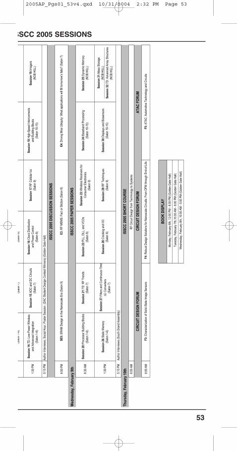
53
SSCC 2005 SESSIONS
(Salo
n 1-
6)(S
alon
7)(S
alon
8)(
)(
)(
)
1:30
PM
Sess
ion
14: T
D: L
ow-P
ower
Wire
less
and
Adva
nced
Inte
grat
ion(S
alon
1-6)
Sess
ion
15:A
DC a
nd D
C Ci
rcuit
s(S
alon
7)
Sess
ion
16: C
lock D
istrib
ution
and
Powe
r Con
trol
(Salo
n 8)
Sess
ion
17: R
F Ce
llular
Ics
(Salo
n 9)
Sess
ion
18: H
igh-S
peed
Inte
rcon
nects
and
Build
ing B
locks
(Salo
n 10
-15)
Sess
ion
19:Im
ager
s(N
OB H
ILL)
5:15
PM
Auth
or In
terv
iews;
Socia
l Hou
r; Po
ster S
essio
n (D
AC S
tude
nt D
esign
Con
test
Winn
ers)
(Gold
en G
ate
Hall)
8:00
PM
Wed
nesd
ay, F
ebru
ary 9
th
8:30
AM
Sess
ion
20: P
roce
ssor
Buil
ding
Bloc
ks
(Salo
n 1-
6)Se
ssio
n 21
:TD:
RF
Tren
ds(S
alon
7)Se
ssio
n 22
:PLL
, DLL
, and
VCO
s(S
alon
8)
Sess
ion
23: W
ireles
s Rec
eiver
s for
Co
nsum
er E
lectro
nics
(Salo
n 9)
Sess
ion
24:B
aseb
and
Proc
essin
g(S
alon
10-1
5)Se
ssio
n 25
:Dyn
amic
Mem
ory
(NOB
HIL
L)
1:30
PM
Sess
ion
26:S
tatic
Mem
ory
(Salo
n 1-
6)
Sess
ion
27: F
ilters
and
Con
tinuo
us-T
ime
Conv
erte
rs(S
alon
7)
Sess
ion
28: C
lockin
g an
d I/O
(Salo
n 8)
Sess
ion
29: R
F Te
chniq
ues
(Salo
n 9)
Sess
ion
30:D
isplay
s and
Bios
enso
rs(S
alon
10-1
5)
Sess
ion
31:M
ass S
tora
ge(N
OB H
ILL)
Sess
ion
32:T
D: A
dvan
ced
Arra
y Stru
cture
s(N
OB H
ILL)
5:15
PM
Auth
or In
terv
iews (
Sout
h Gr
and
Asse
mbly
)
Thur
sday
, Feb
ruar
y 10t
h
8:
00 A
M
8:00
AM
Wed
nesd
ay, F
ebru
ary 8
th, 1
0:00
AM
- 5:
00 P
M (G
olden
Gat
e Ha
ll)
CIRC
UIT
DESI
GN F
ORUM
F3: C
hara
cteriz
ation
of S
olid-
Stat
e Im
age
Sens
ors
F5: A
TAC:
Aut
omot
ive T
echn
ology
and
Circ
uits
F4: R
obus
t Des
ign S
olutio
ns fo
r Nan
osca
le Ci
rcuit
s: Fr
om D
FM th
roug
h En
d-of
-Life
RF C
ircuit
Des
ign fr
om T
echn
ology
to S
yste
ms
SE5:
SRAM
Des
ign in
the
Nano
scale
Era
(Salo
n 9)
E3:R
F M
EMS:
Fac
t or S
tictio
n (S
alon
8)E4
: Driv
ing M
iss U
biquit
y: W
hat a
pplic
ation
s will
fill to
mor
row’
s fab
s? (S
alon
7)
ISSC
C 20
05 D
ISCU
SSIO
N SE
SSIO
NS
ATAC
FOR
UMCI
RCUI
T DE
SIGN
FOR
UM
ISSC
C 20
05 P
APER
SES
SION
S
Tues
day,
Febr
uary
7th
,10:
00 A
M -
8:00
PM
(Gold
en G
ate
Hall)
BOOK
DIS
PLAY
Mon
day,
Febr
uary
6th
, 12:
00 P
M -
8:00
PM
(Gold
en G
ate
Hall)
ISSC
C 20
05 S
HORT
COU
RSE
2005AP_Pgs01_53v4.qxd 10/31/2004 2:32 PM Page 53
54
SESSION 18 SALON 10-15
HIGH-SPEED INTERCONNECTS AND BUILDING BLOCKS
Chair: Vadim Gutnik, Impinj, Newport Beach, CAAssociate Chair: Michael Green, University of California, Irvine. CA
18.1 A 10Gb/s CMOS Adaptive Equalizer for Backplane Applications
1:30 PMS. Gondi1, J. Lee2, B. Razavi11University of California, Los Angeles, CA2National Taiwan University,Taepei, Taiwan,
An equalizer employs reverse scaling and dual-loop adaptation to achievea binary data rate of 10Gb/s. Realized in 0.13µm CMOS technology, thecircuit adapts to traces up to 30 inches on FR4 boards while consuming25mW from a 1.2V supply.
18.2 A 7-Tap Transverse Analog FIR Filter in 0.12µm CMOS for Equalization of 10Gb/s Fiber-Optic Data Systems
2:00 PMS. Reynolds, P. Pepeljugoski, J. Schaub, J. Tierno, D. BeisserIBM, Yorktown Heights, NY
A 130mA 2.5V 7-tap analog FIR equalizer for 10Gb/s fiber-optic links isimplemented in a 0.12µm CMOS process. The filter precedes the receiverCDR and recovers data signals distorted by multi-mode fiber dispersionover a 600m link to a BER <10-12. Tap delays are implemented by a combination of passive and buffered LC transmission lines.
18.3 A 10 Gb/s Eye-Opening Monitor in 0.13µm CMOS2:30 PM
B. Analui1, A. Rylyakov2, S. Rylov2, A. Hajimiri11California Institute of Technology, Pasadena, CA2IBM, Yorktown Heights, NY
An eye-opening monitor circuit in 0.13µm CMOS operates from 1 to12.5Gb/s at 1.2V supply. It maps the input eye to a 2D error diagram with68dB mask error dynamic range. Left and right half of the eye are monitored separately to capture asymmetric eyes. Tested input amplitudeis from 50 to 400mV. The chip consumes 330mW and works at 10Gb/swith a supply voltage as low as 1V.
BREAK 3:00 PM
18.4 A 100mW 4x10Gb/s Transceiver in 80nm CMOS for High-Density Optical Interconnects
3:15 PMC. Kromer1, G. Sialm1, C. Berger2, T. Morf2, F. Ellinger1, M. Schmatz2,D. Erni1, G-L. Bona2, H. Jäckel11Swiss Federal Institute of Technology, Zürich, Switzerland2IBM, Rüschlikon, Switzerland
A quad-optical transceiver in 80nm CMOS transmits 10Gb/s/ channel overa multi-mode fiber at a BER of <10-12. Each driver consumes 2mW from a0.8V supply and a VCSEL requires 7mA from a 2.4V supply. The receiverexcluding the output buffer consumes 6mW from a 1.1V supply per channel and features a transimpedance gain of 10.1kΩ.
2005AP_Pgs54_104v4.qxd 10/31/2004 3:12 PM Page 54
55
Tuesday, February 8th 1:30 PM
18.5 A 0.25µm CMOS 3b 10GS/s Frequency ChannelizedReceiver for Serial-Links
3:45 PMK. Lee, W. NamgoongUniversity of Southern California, Los Angeles, CA
A frequency channelized receiver that samples at an effective samplingfrequency of 10GS/s with 3b resolution is fabricated in a 0.25µm CMOSprocess. The chip occupies 4mm2 and consumes 1W at 2.5V supply. Thefunctionality of the receiver is demonstrated by correctly reconstructingdata from 10GS/s in a channel with significant ISI.
18.6 An RF/Baseband FDMA-Interconnect Transceiver forReconfigurable Multiple Access in Chip-to-Chip Communication
4:15 PMJ. Ko1, J. Kim1, Z. Xu2, Q. Gu1, C. Chien1,2, M. Chang1
1University of California, Los Angeles, CA2SST Communications, Los Angeles, CA
An RF/baseband FDMA-interconnect transceiver, implemented in 0.18µmCMOS, enables reconfigurability and multiple access for multi-I/Os on ashared bus. The RF/baseband transceiver achieves an aggregate datarate of 3Gb/s/pin (3.6Gb/s/pin) for bi-directional (uni-directional) signalingwhile dissipating 92mW and occupying 0.65mm2.
18.7 A 40Gb/s 2.5V 27-1 PRBS Generator in SiGe Using a Low-Voltage Logic Family
4:45 PMD. Kucharski, K. KornegayCornell University, Ithaca, NY
A 40Gb/s PRBS generator with a sequence length of 27-1 is implementedin a SiGe BiCMOS process with fT=120GHz. It consumes 550mW from a2.5V supply. Low-voltage operation is achieved through the use of analternative family of logic gates with reduced device stacking.
18.8 A 72Gb/s 231-1 PRBS Generator in SiGeBiCMOS Technology
5:00 PMT. Dickson1, E. Laskin1, I. Khalid2, R. Beerkens2, J. Xie2, B. Karajica2, S. Voinigescu1
1University of Toronto, Toronto, Canada2STMicroelectronics, Ottawa, Canada
A 231-1 72Gb/s PRBS generator is reported in a 0.13µm SiGe BiCMOStechnology with 150GHz-fT HBTs. Variable delays are introduced along the36GHz clock path to increase timing margins. A true BiCMOS logic familyusing NMOS FETs in the clock path is employed throughout the circuit, which dissipates 9.28W from a 3.3V supply to provide a single-ended output swing of 300mV at 72Gb/s.
CONCLUSION 5:15 PM
2005AP_Pgs54_104v4.qxd 10/31/2004 3:12 PM Page 55
56
SESSION 19 NOB HILL
IMAGERS
Chair: Abbas El Gamal, Stanford University, Stanford, CAAssociate Chair: Hirofumi Sumi, Sony, Kanagawa, Japan
19.1 A 1/4.5” 3.1M Pixel FT-CCD with 1.56µm Pixel Size for Mobile Applications
1:30 PMM. Oda, T. Kaida, S. Izawa, T. Ogo, K. Itsumi, Y. Okada, K. SasadaSanyo Electric, Gifu, Japan
The frame-transfer CCD (FT-CCD) achieves a saturation signal voltage of270mV and a sensitivity of 280mV/lx⋅s in full-resolution still mode. The sensorcan also operate in a 30f/s VGA with a movie mode with saturation signal voltage of 1040mV and a sensitivity of 960mV/lx⋅s. A 9-phase vertical transfertechnique reduces smear signals to -75dB.
19.2 A 2.0µm Pixel-Pitch MOS Image Sensor with an Amorphous Si Film Color Filter
2:00 PMM. Kasano, Y. Inaba, M. Mori, S. Kasuga, T. Murata, T. YamaguchiMatsushita, Kyoto, Japan
A CMOS image sensor with an amorphous Si film color filter is implemented ona standard Si process. The color filter thickness is less than 100nm. The sensor achieves a 30% aperture ratio by a 1.5transistor/pixel architecture anda 0.15µm design rule.
19.3 A 19.5b DR CMOS Image Sensor with 12bColumn-Parallel Cyclic A/D Converters
2:15 PMM. Mase1, S. Kawahito1, M. Sasaki2, Y. Wakamori31Shizuoka University, Shizuoka, Japan2Sendai National College of Technology, Miyagi, Japan3Yamaha, Shizuoka, Japan
A CMOS image sensor with 117dB DR is demonstrated in a 0.25µm CMOStechnology through merging of multiple exposures. A 12b cyclic ADC with integrated noise canceling is implemented in the column of the image sensorand achieves a DNL of +0.4/-0.8 LSB.
19.4 A 100dB DR CMOS Image Sensor Using a LateralOverflow Integration Capacitor
2:30 PMS. Sugawa1, N. Akahane1, S. Adachi2, K. Mori2, T. Ishiuchi2, K. Mizobuchi21Tohoku University, Miyagi, Japan2Texas Instruments, Ibaragi, Japan
The wide DR CMOS image sensor incorporates a lateral overflow capacitor ineach pixel to integrate the overflow charges from the photodiode when it saturates. The 7.5×7.5µm2 pixel, 1/3" VGA sensor fabricated in a 0.35µm 3M2PCMOS process achieves a 100dB dynamic range with no image lag, 0.15mVrms
random noise and 0.15mV fixed pattern noise.
19.5 A Linear-Logarithmic CMOS Sensor with Offset Calibration Using an Injected Charge Signal
2:45 PMK. Hara, H. Kubo, M. Kimura, F. Murao, S. KomoriRenesas Technology, Hyogo, Japan
A combined linear and logarithmic image sensor is implemented in a 0.35µm1P3M technology. The pixel is 7.5x7.5µm2 with a 37% fill factor and containsonly 4 transistors. Offset calibration in the logarithmic region is realized byusing electrical charge injection into the photodiode. The sensor achieves120dB DR and the offset calibration reduces the FPN from 13mV to 5mV.
BREAK 3:00 PM
2005AP_Pgs54_104v4.qxd 10/31/2004 3:12 PM Page 56
57
Tuesday, February 8th 1:30 PM
19.6 Megapixel CMOS Image Sensor Fabricated in Three-Dimensional Integrated Circuit Technology
3:15 PMV. Suntharalingam, R. Berger, J. Burns, C. Chen, C. Keast, J. Knecht, R. Lambert, K. Newcomb, D. O'Mara, D. Rathman, D. Shaver, A. Soares, C. Stevenson, B. Tyrrell, K. Warner, B. Wheeler, D. Yost, D. YoungMIT Lincoln Laboratories, Lexington, MA
A 1024x1024 integrated image sensor with 8µm pixels, is developed with 3D fabrication in 150mm wafer technology. Each pixel contains a 2µmx2µmx7.5µm3D via to connect a deep depletion, 100% fill-factor photodiode layer to a fullydepleted SOI CMOS readout circuit layer. Pixel operability exceeds 99.9%, andthe detector has a dark current of <3nA/cm2 and pixel responsivity of ~9µV/e atroom temperature.
19.7 A Progressive 1920x1080 Imaging SoC for HDTV Cameras3:45 PM
L. Kozlowski, G. Rossi, L. Blanquart, R. Marchesini, Y. Huang, G. Chow, J. RichardsonAltaSens, Thousand Oaks, CA
A 2/3” 5µmx5µm pixel HDTV imager in a 0.25µm CMOS process uses atapered reset technique to suppress kT⁄C noise and supply 12b video with <15e-read noise at 60, 72 and 90Hz frame rates. Peak S/N ratio at 90Hz(225MHzvideo rate; 2.7Gb/s at 12b/pixel) is 52dB at standard scene illumination.Random noise at 18dB gain is 8e-, independent of video frequency.
19.8 A High-Speed Profile Data Acquiring Image Sensor 4:15 PM
Y. Sugiyama, M. Takumi, H. Toyoda, N. Mukozaka, A. Ihori, T. Kurashina, Y. Nakamura, T. Tonbe, S. MizunoHamamatsu Photonics, Shizuoka, Japan
A profile imager for high-speed automatic target tracking has the capability ofexecuting both target-tracking control from a 512x512 image array of20µmx20µm pixels and the acquisition of a sub-array, simultaneously. 128x128partial images of an automobile license plate can be captured at 1620f/s. A0.6µm 3M2P CMOS process is used to implement the 13.0mm×14.3mm imager.
19.9 Temporal Change Threshold Detection Imager4:45 PM
U. Mallik, M. Clapp, E. Choi, G. Cauwenberghs, R. Etienne-CummingsJohns Hopkins University, Baltimore, MD
A 90x90 active pixel sensor (APS) achieves 2% in-pixel change/motion detection at 30f/s consuming 4.2mW. The 6T 2C 25µmx25µm pixel in 0.5µm2P3M CMOS provides intensity readout, detection of change events and polar-ities. Event address and APS value output are asynchronous, facilitating compression. The imager is intended for low-power low-bandwidth surveillancenetwork applications.
19.10 A Single Photon Detector Array with 64x64 Resolution and Millimetric Depth Accuracy for 3D Imaging
5:00 PMC. Niclass, E. CharbonEcole Polytechnique Federale de Lausanne, Lausanne, Switzerland
An avalanche photodiode array uses single-photon counting to perform time-of-flight range-finding on a scene uniformly hit by 100ps 250mW uncollimatedlaser pulses. The 32x32 pixel sensor, fabricated in a 0.8µm CMOS processuses a microscanner package to enhance the effective resolution in the appli-cation to 64x64 pixels. The application achieves a measurement depth resolu-tion of 1.3mm to a depth of 3.75m.
CONCLUSION 5:15 PM
2005AP_Pgs54_104v4.qxd 10/31/2004 3:12 PM Page 57

58
DISCUSSION SESSIONS
SE5: SRAM Design in the Nanoscale Era
(Salon 9)
Organizer: Sreedhar Natarajan, MoSys, Stittsville, CanadaChair: Alexander Shubat, Virage Logic, Fremont, CA
The geometries of SRAMs have shrunk substantially over the years.SRAMs have been the mainstream embedded memory for most applica-tions (processors, graphics, etc.), although a new suite of replacements isbeing researched. In the sub-90nm era, SRAMs face a new set of issuesthat need to be addressed and solved in the areas of design, test andprocess. Twenty years ago, soft errors emerged as a problem for DRAMs,which store data in a single capacitor. This was not a concern for SRAMs.Soft error rates (SER) are caused when a neutron, alpha particle or someother ionizing particle strikes a solid-state memory and may degrade thestored data. As transistor geometries have shrunk, SER becomes a muchbigger issue in SRAMs. Considering the incredibly high wafer cost, thereis not much incentive for companies to spin multiple silicon shuttles andhence, have to ensure the design is equipped with Design for Testability(DFT) capabilities. Robust dynamic and static circuits and design marginsare also key for proper functionality. Leakage is another critical concern forpower-aware systems and innovative circuit techniques are required toaddress the standby leakage.The experienced speakers address leakage,DFT and SER issues in SRAMs.
Time Topic
8:00 SRAM Design in 90nm Era,Harold Pilo, IBM, Essex Junction, VT
8:30 Test Solutions to Improve SRAM Yield,Yervant Zorian, Virage Logic, Fremont, CA
9:00 SER in SRAMs,Robert Baumann, Texas Instruments, Dallas, TX
9:30 SRAM Leakage-Reduction Techniques,Soon Moon Jung, Samsung, Yongin-City, Korea
2005AP_Pgs54_104v4.qxd 10/31/2004 3:12 PM Page 58
59
Tuesday, February 8th 8:00 PM
E3: RF MEMS: Fact or Stiction
(Salon 8)
Organizer: Ken Cioffi, Discera, San Jose, CA Moderator: Bob Puers, Katholieke Universiteit Leuven,
Leuven Belgium
RF MEMS components including switches, varactors, inductors, resonators,and filters have been proposed for use in RF systems. Can these compo-nents replace traditional technologies such as semiconductor switches,quartz crystals, and SAW resonators or will manufacturability/cost/perform-ance issues keep them always on the horizon? Alternatively, will advancedcircuit techniques make many of these components obsolete before theycome to market or will RF MEMS play a key role in determining new circuittopologies?
Panelists:
Natalino Camilleri, RF & Wireless Design Services,Cupertino, CA
Dan Hyman, XCom Wireless, Signal Hill, CABill Krenik, Texas Instruments, Dallas, TX Clark T.-C. Nguyen, DARPA, Arlington, VA and
University of Michigan, Ann Arbor, MITomoki Uwano, Matsushita, Osaka, JapanBenedetto Vigna, ST Microelectronics, Milano, Italy
E4: Driving Miss Ubiquity: What applications will fill tomorrow’s fabs?
(Salon 7)
Organizer: Toru Shimizu, Renesas Technology, Tokyo, JapanModerator: Robert Brodersen, University of California,
Berkeley, CA
The objective of this panel is to describe the applications that will drive thedemand for advances in silicon technology and integrated circuit design. Thepanelist will debate the merits and universal appeal of several applications suchas body area networks, smart dust, ambient intelligence, cell phones, RFIDtags, and ubiquitous networks.
Panelists:Gerard Beenker, Philips,
Eindhoven, The NetherlandsRobert Glidden, Impinj, Seattle, WABert Gyselinckx, IMEC, Leuven, BelgiumRyo Imura, Hitachi, Tokyo, JapanHirotaka Nakano, Osaka University, Osaka, JapanKristofer S.J. Pister, Dust Networks, Berkeley, CA
2005AP_Pgs54_104v4.qxd 10/31/2004 3:12 PM Page 59
60
SESSION 20 SALON 1-6
PROCESSOR BUILDING BLOCKS
Chair: Atila Alvandpour, Linkoping University, Linkoping, Sweden
Associate Chair: Fumio Arakawa, Hitachi, Tokyo, Japan
20.1 An 8GHz Floating Point Multiply8:30 AM
W. Belluomini, D. Jamsek, A. Martin, C. McDowell, R. Montoye, T. Nguyen, H. Ngo, J. Sawada, I. Vo, R. DattaIBM, Austin, TX
The implementation of the mantissa portion of a floating-point multiply(54x54b) is described. The 0.124mm2 multiplier is implemented using limited switch dynamic logic and operates at speeds up to 8GHz in a 90nmSOI technology. The multiplier dissipates between 150mW and 1.8W as itscales between 2GHz and 8GHz.
20.2 A 110GOPS/W 16b Multiplier and Reconfigurable PLALoop in 90nm CMOS
9:00 AMS. Hsu, S. Mathew, M. Anders, B. Bloechel, R. Krishnamurthy, S. BorkarIntel, Hillsboro, OR
A 16b 2's-complement multiplier with a reconfigurable PLA control block isfabricated in a 90nm dual-Vt CMOS process and occupies 0.03mm2. It per-forms 1GHz single-cycle operations and dissipates 9mW to deliver110GOPS/W at 1.3V, and is frequency scalable to 1.5GHz at 1.95V. PMOSsleep transistors enable an ultra low standby-mode power of 75µW withwake-up time < 1 cycle.
20.3 A Double-Precision Multiplier with Fine-Grained Clock-Gating Support for a First-Generation CELL Processor
9:30 AMJ. Kuang1, T. Buchholtz2, S. Dance2, J. Warnock3, S. Storino2, D. Wendel41IBM, Austin, TX2IBM, Rochester, MN3IBM, Yorktown Heights, NY4IBM, Böblingen, Germany
A double-precision multiplier for a 90nm SOI CELL processor is presented. Dynamic Booth logic is designed for scalability and with noise,leakage, and pulse-width variation tolerance. Static partial-product compression is implemented with replicated bits for performance. Thedesign supports fine-grained clock gating domains for active power reduc-tion.
BREAK 10:00 AM
20.4 A Low-Leakage 2.5GHz Skewed CMOS 32b Adder forNanometer CMOS Technologies
10:15 AMK. von Arnim1,2, P. Seegebrecht2, R. Thewes1, C. Pacha1
1Infineon Technologies, Munich, Germany2Christian Albrecht University, Kiel, Germany
A 32b parallel prefix adder demonstrates leakage-current-reduction capabilities of skewed CMOS logic. Sub-100nA leakage currents and single-cycle activation from standby mode is achieved using multi-tox logicgates in 90nm CMOS technology. The data path contains improved senseamplifier-based flip-flops and skewed CMOS logic adapted latches.
2005AP_Pgs54_104v4.qxd 10/31/2004 3:12 PM Page 60
61
Wednesday, February 9th 8:30 AM
20.5 The Multi-threaded Parity-Protected 128-Word RegisterFiles on a Dual-Core Itanium®-Family Processor
10:45 AML. Wang1, E. Fetzer2, J. Jones3
1University of Connecticut, Storrs, Connecticut2Hewlett Packard, Fort Collins, CO3Intel, Fort Collins, CO
The dual-thread 18-port 128wx82b FPU register file, and the 22-port128wx65b integer register file of the microprocessor is described. Parityembedded into each register provides soft error detection. The design integrates a charge-compensated thread switch and power-saving features to operate at 1.1V consuming 400mW at maximum frequency.
20.6 A 32b 64-Word 9-Read-Port/7-Write-Port Pseudo Dual-Bank Register File Using Copied Memory Cells for a Multi-Threaded Processor
11:15 AMM. Sumita, Y. IkedaMatsushita, Kyoto, Japan
A method for copying memory cells to reduce the size of the register filefor a multi-threaded processor is proposed. The number of transistors inthe memory cell is reduced to 70% and the total bit and word lines isreduced to 63%. The register file is implemented in a 100nm CMOSprocess. The size of the register file is reduced to 62% of a conventionalregister file. The power consumption is reduced by 50%.
20.7 A 3Gb/s/ch Transceiver for RC-limited On-Chip Interconnects
11:45 AMD. Schinkel1, E. Mensink1, E. Klumperink1, E. van Tuijl1,2, B. Nauta1
1University of Twente, Enschede, The Netherlands2Philips, Eindhoven, The Netherlands
A bus-transceiver chip in 0.13µm CMOS uses 10mm uninterrupted differential interconnects of 0.8µm pitch (82MHz RC-limited bandwidth).The chip achieves 3Gb/s/ch using a pulse-width pre-emphasis techniquein combination with resistive termination while twisted interconnects miti-gate crosstalk. Power consumption is 6mW/ch at a 1.2V supply.
CONCLUSION 12:15 PM
2005AP_Pgs54_104v4.qxd 10/31/2004 3:12 PM Page 61
62
SESSION 21 SALON 7
TD: RF TRENDS: ABOVE-IC INTEGRATION AND MM-WAVE
Chair: Ernesto Perea, ST Microelectronics, Crolles, FranceAssociate Chair: Christian Enz, CSEM, Neuchatel, Switzerland
21.1 Tunable RF and Analog Circuits Using On-Chip MEMSPassive Components
8:30 AMG. Fedder, T. MukherjeeCarnegie Mellon University, Pittsburgh, PA
Micromachining in RF foundry processes enhances inductor and capacitor quality factors, increases varactor tuning range, and supportscreation of electromechanical mixer-filters that down-convert RF signalsfrom GHz to MHz frequency band with built-in frequency selectivity. An on-chip parallel receiver architecture and circuit blocks incorporating theseMEMS devices for low-power operation are presented.
21.2 Integration of High-Q BAW Resonators and Filters above IC
9:00 AMM. Dubois1, C. Billard2, C. Muller1, G. Parat2, P. Vincent2
1Swiss Centre of Electronics and Microtechnology, Neuchâtel, Switzerland
2CEA - LETI, Grenoble, France
A double-lattice BAW filter with balanced input and output is designed witha center frequency of 2.14GHz. The filter is integrated directly above a0.25µm BiCMOS RF IC. Insertion loss of -3dB and out-of-band rejection better than -50dB are achieved. An integrated LNA comprisingtwo broadband amplifiers and one BAW filter is also presented.
21.3 A SiGe:C BiCMOS WCDMA Zero-IF RF Front-End Using anAbove-IC BAW Filter
9:30 AMJ-F. Carpentier1, A. Cathelin1, C. Tilhac1, P. Garcia1, P. Persechini1, P. Conti2,P. Ancey1, G. Bouche1, G. Caruyer1, D. Belot1, C. Arnaud1, C. Billard3, G. Parat3, J-B. David3, P. Vincent3, M-A. Dubois4, C. Enz4
1STMicroelectronics, Crolles, France2STMicroelectronics, Plan-les-Ouates, Switzerland3CEA - LETI, Grenoble, France4Swiss Centre of Electronics and Microtechnology,
Neuchatel, Switzerland
The feasibility of a fully integrated RF front-end using an above-IC BAWintegration technique is demonstrated for WCDMA applications. The circuit has a voltage gain of 31.3dB, a noise figure of 5.3dB, an in-bandIIP3 of -8dBm and IIP2 of 38dBm, with a total power consumption of36mW. The BAW filter area is 0.45mm2 and the total circuit area includingthe BAW filter is 2.44mm2.
21.4 A 450µW-RX 1.6mW-TX Super-Regenerative Transceiverfor Wireless Sensor Networks
9:45 AMB. Otis, Y-H. Chee, J. RabaeyUniversity of California, Berkeley, CA
A fully-integrated 2GHz super-regenerative transceiver is implemented ina 0.13µm CMOS process. The transmit and receive paths utilize BAW resonators, yielding a 450µW 1V RF front-end and a transmitter delivering380µW with 23% efficiency. At 5kb/s, the receiver achieves a sensitivity of-100.5dBm for 10-3 BER.
BREAK 10:00 AM
2005AP_Pgs54_104v4.qxd 10/31/2004 3:12 PM Page 62
63
Wednesday, February 9th 8:30 AM
21.5 Thin Film as Enabling Passive Integration Technology for RF SoC and SiP
10:15 AMG. Carchon, X. Sun, G. Posada, D. Linten, E. BeyneIMEC, Leuven, Belgium
Thin-film Cu/BCB technology with integrated inductors, resistors andcapacitors is described for the realization of high-quality on-chip and in-package Si-based passive elements. Thin-film SiP and SoC inductorand transmission line performances are compared. A SiP 7GHz powersplitter, a 50GHz BPF, and two 90nm CMOS VCOs operating at 5.8GHzand 15GHz with on-chip thin-film inductors are discussed.
21.6 A 60GHz Direct-Conversion CMOS Receiver10:45 AM
B. RazaviUniversity of California, Los Angeles, CA
A direct-conversion receiver incorporates folded microstrip lines to createresonance at 60GHz in a common-gate LNA and active mixers. Realizedin 0.13µm CMOS technology, it provides a voltage gain of 28dB with12.5dB NF while consuming 9mW from a 1.2V supply.
21.7 A 70GHz Cascaded Multi-Stage Distributed Amplifier in90nm CMOS Technology
11:15 AMM-D. Tsai1, H. Wang1, J-F Kwan2, C-S Chang2, 1National Taiwan University, Taipei, Taiwan2TSMC, Hsin-Chu, Taiwan
A broadband cascaded multi-stage distributed amplifier (CMSDA) is implemented in a standard 90nm CMOS technology. The 0.72mm2 CMOScascaded multi-stage distributed amplifier achieves better than 7dB gainwith a bandwidth of 70GHz, 10dBm output power for 1dB compression at30GHz, 9.3dBm IIP3 at 40GHz and 6.4dB average NF from 1 to 25GHz.
21.8 A 114GHz VCO in 0.13µm CMOS Technology11:45 AM
P-C. Huang1, M-D. Tsai1, H. Wang1, C-S Chang2
1National Taiwan University, Taipei, Taiwan2TSMC, Hsin-Chu, Taiwan
A D-band (110 to 170GHz) CMOS VCO is presented.This push-push VCOimplemented in standard 0.13µm CMOS technology has a 114GHz outputsignal with a phase noise of -107.6dBc/Hz at 10MHz offset and power con-sumption of 8.4mW from a 1.2V supply.
21.9 A Fully Integrated BiCMOS PLL for 60GHz WirelessApplications
12:00 PMW. Winkler, J. Borngräber, B. Heinemann, F. HerzelIHP, Frankfurt (Oder), Germany
An integrated PLL aimed at wireless transceivers in the unlicensed band from 59GHz to 64GHz is described. The PLL was fabricated in aSiGe:C BiCMOS technology with both fT/fmax=200GHz. The measured PLLlock range is from 53.3GHz to 55.7GHz. It operates from a 3V supplyexcept for a first divide-by-two stage which requires a 5V supply. Totalpower consumption is 895mW.
CONCLUSION 12:15 PM
2005AP_Pgs54_104v4.qxd 10/31/2004 3:12 PM Page 63
64
SESSION 22 SALON 8
PLL, DLL, AND VCOs
Chair: Roger Minear, Agere Systems, Wyomissing, PAAssociate Chair: Thomas Burger, Swiss Federal Institute of
Technology, Zurich, Switzerland
22.1 A 0.94ps-rms-Jitter 0.016mm2 2.5GHz Multi-PhaseGenerator PLL with 360° Digitally Programmable Phase Shift for 10Gb/s Serial Links
8:30 AMT. Toifl1, C. Menolfi1, P. Buchmann1, M. Kossel1, T. Morf1, M. Ruegg2, R. Reutemann2, M. Schmatz1, J. Weiss1
1IBM, Rueschlikon, Switzerland2Miromico, Zurich, Switzerland
A PLL generates 8 equidistant clock phases whose timing with respect toa reference clock can be simultaneously shifted in 3ps steps by a digitalvalue. Each VCO phase is fed to a dedicated phase detector and theweighted dectector outputs are summed. Fabricated in 90nm SOI-CMOStechnology, the PLL has a jitter of 0.94psrms at 2.5GHz and consumes20mW from a 0.9V supply.
22.2 A 15mW 3.125GHz PLL for Serial Backplane Transceivers in 0.13µm CMOS
9:00 AMJ. Parker1, D. Weinlader2, J. Sonntag1
1Synopsys, Hillsboro, OR2Synopsys, Allentown, PA
A 3.125GHz PLL fabricated in a 0.13µm CMOS process in a area of0.064mm2 is described. The PLL uses an architecture optimized for lownoise, low power and small die area. In steady-state operation, the PLLforces the up and down currents in the charge pump to match one anoth-er. The total measured jitter is 1.3ps rms when operating at 3.125GHz andthe chip consumes 15mW.
22.3 A Low-Jitter Wideband Multi-Phase PLL9:30 AM
M. Kossel, P. Buchmann, C. Menolfi, T. Morf, T. Toifl, M. SchmatzIBM, Rueschlikon, Switzerland
A multi-phase PLL, implemented in 90nm SOI CMOS, covers a frequencyrange from 4.3 to 7.4GHz at a supply voltage of 1V. The ring-oscillator-based PLL shows an in-band phase noise of up to -113dBc/Hz at 1 MHzoffset and a supply noise rejection of 0.23%delay/%supply due to the rigorous application of CML-type circuit topologies combined with replicabiasing.
BREAK 10:00 AM
22.4 A 44GHz Differentially Tuned VCO with 4GHz Tuning Range in 0.12µm SOI CMOS
10:15 AMJ. Kim, J-O. Plouchart, N. Zamdmer, R. Trzcinski, K. Wu, B. Gross, M. KimIBM, Hopewell Junction, NY
A differentially tuned VCO is fully integrated in a standard microprocessor0.12µm SOI CMOS. A phase noise of -101.8dBc/Hz at 1MHz offset ismeasured with 7.5mW at 1.5V. The VCO tuning range is 9.8% from 40GHzto 44GHz. The output power is up to -6dBm after a single-stage bufferamplifier with 6mW at 1.5V.
2005AP_Pgs54_104v4.qxd 10/31/2004 3:12 PM Page 64
65
Wednesday, February 9th 8:30 AM
22.5 A Low-Phase-Noise 0.004ppm/Step DCXO with GuaranteedMonotonicity in 90nm CMOS
10:45 AMJ-C. LinTexas Instruments, Plano, TX
A 26MHz DCXO achieves phase noise of -140dBc/Hz at 1kHz, -152dBc/Hz at 10kHz offset, and supply pushing of 0.5ppm/V. Frequencytuning is done by a pre-distorted 14b MOS capacitor DAC. Monotonicity of~0.004ppm/step across the entire 70ppm tuning range is guaranteed by a∆Σ modulation scheme. The circuit occupies 0.18mm2 in 90nm CMOS.
22.6 A Self-Biased PLL With Current-Mode Filter for Arbitrary Clock Generator
11:15 AMG. Yan, C. Ren, Z. Guo, Q. Ouyang, Z. ChangIntegrated Device Technology, Shanghai, China
A self-biased PLL with current mode filter is designed to achieve a bandwidth that scales with reference clock and is independent of PVT andmultiplication factor. It provides wide tuning range with a simple robuststructure. The 0.2mm2 chip is fabricated in 0.35µm CMOS. Running at800MHz, the phase jitter is 72.7pspp and the power consumption is 20mW.
22.7 An Ultra-Low-Power Fast-Lock-in Small-Jitter All-Digital DLL
11:45 AMJ-S. Wang, Y-M. Wang, C-H. Chen, Y-C. LiuChung-Cheng University, Chia-Yi, Taiwan
Using binary-weighted differential-delay cells and an asynchronous binarysearch circuit, the proposed 1.0V 0.25µm all-digital DLL achieves nearly 2 orders of magnitude reduction in power consumption, a 36% reductionin jitter, and a 33% reduction in locking cycles, compared to conventionalfast-lock mixed-mode DLLs.
CONCLUSION 12:15 PM
2005AP_Pgs54_104v4.qxd 10/31/2004 3:12 PM Page 65
66
SESSION 23 SALON 9
WIRELESS RECEIVERS FOR CONSUMER ELECTRONICS
Chair: John R. Long, Delft University of Technology, Delft, The Netherlands
Associate Chair: Tony Montalvo, Analog Devices, Raleigh, NC
23.1 A Direct-Conversion Receiver for DVB-H8:30 AM
N. Kearney1, P. Antoine2, P. Bauser3, B. Hugues2, M. Buchholz4, D. Carey1,T. Cassagnes2, T. Chan1, S. Colomines2, F. Hurley1, D. Jobling3, A. Murphy1,J. Rock1, D. Salle2, C-T. Tu3
1Freescale Semiconductor, Cork, Ireland2Freescale Semiconductor, Toulouse, France3Freescale Semiconductor, Geneva, Switzerland4Freescale Semiconductor, Munich, Germany
A 240mW direct-conversion DVB-H receiver in a 0.35µm BiCMOS processis presented. The receiver covers UHF bands IV and V, and exhibits anominal 80dB gain, 8.5dB NF, and 8.5dBm IIP3. The IC includes an LNA,dual quadrature mixers, base-band filtering, three 4x VCOs, an integerPLL, and a reference oscillator.
23.2 UMTV: a Single Chip TV Receiver for PDAs,PCs and Cell-Phones
9:00 AMH. Rumpt1, D. Kasperkovitz1, J. van der Tang2, B. Nauta3
1ItoM, Eindhoven, The Netherlands2Eindhoven University of Technology, Eindhoven, The Netherlands3University of Twente, Enschede, The Netherlands
A zero-external-component TV receiver for portable platforms is realized ina mainstream 8GHz-fT BiCMOS process. Die size is 5×5mm2 and power dissipation is 50mA at 3V. The receiver includes a single tunable LNA(3mA) with less than 5dB NF from 40 to 900MHz. The programmable IF fil-ters cover all analog and digital standards.
23.3 A 120nm CMOS DVB-T Tuner9:30 AM
D. Saias, F. Montaudon, E. Andre, M. Bely, P. Busson, S. Dedieu, A. Dezzani, A. Moutard, G. Provins, E. Rouat, J. Roux, G. Wagner, F. PaillardetSTMicroelectronics, Crolles, France
A DVB-T tuner is integrated in 0.12µm CMOS. The 16mm2 chip integratesa double conversion chain including PLL, VCOs, voltage regulators, andADC. The receiver exhibits a 6.5dB NF, a VCO phase noise of -140dBc/Hzat 1MHz offset at 1.21GHz, and a 14b ADC. It is compatible for integration with a digital demodulator IP.
Break 10:00 AM
2005AP_Pgs54_104v4.qxd 10/31/2004 3:12 PM Page 66
67
Wednesday, February 9th 8:30 AM
23.4 A CMOS TV Tuner/Demodulator IC with Digital Image Rejection
10:15 AMC-H. Heng1, M. Gupta1, S-H. Lee1, D. Kang1, B-S. Song2
1Chrontel, San Diego, CA2University of California, San Diego, CA
A single-chip TV tuner/demodulator IC using a low-IF dual-conversionarchitecture is implemented. It receives the NTSC/PAL/SECAM signals inthe 48 to 860MHz frequency range without off-chip image filters, and performs channel selection, image rejection, and video/sound demodulation digitally. The 6x6mm2 chip in 0.25µm CMOS with on-chip75Ω cable driver consumes 1W from a 2.5V supply.
23.5 A Compact Triple-Band Eureka-147 RF Tuner with an FM Receiver
10:45 AMG. Luff, S. Tuncer, N. Troop, C. Taylor, D. EddowesFrontier Silicon, Cambridge, United Kingdom
A 0.35µm SiGe BiCMOS single-chip RF tuner for DAB and DMB receivesDAB signals in both L-Band and Band 3, and FM broadcast signals onBand 2. The chip contains a VCO, integer-N PLL, multi-band LNA with anAGC, quadrature mixer, IF filter, IF AGC amplifier and supply regulators.The 2.5mmx2.5mm die has a sensitivity of -100dBm in Band 3, is packaged in a 5mm×5mm QFN-32, and consumes 150mW from a 3V sup-ply.
23.6 A 2.3GHz SiGe RF IC Front-End for Satellite Radio Applications
11:15 AMR. Pelleriti1, G. Cali`1, R. Camden2, P. De Vita1, S. Geraci1, A. Palleschi1, M. Paparo1, C. Schiro`1, A. Bruno1
1STMicroelectronics, Catania, Italy2XM Satellite Radio, Boca Raton
A 0.35µm SiGe BiCMOS double-conversion digital audio satellite radioreceiver with on-chip RF and IF PLLs is presented. The 17mm2 front-endhas -97dBm input sensitivity, 3.5dB NF, -13dBm off-channel IIP3 at maximum RF gain and 12dBm at minimum RF gain, 35dB RF and 90dBIF gain range, with >30dB image rejection and 30dBm on-channel OIP3.The RF VCO features a phase noise of -107dBc/Hz at 100kHz offset.
23.7 A Single-Chip Receiver for Multi-User Low-Noise Block Down-Converters
11:45 AMT. Copani1, S. Smerzi2, G. Girlando2, G. Ferla2, G. Palmisano1
1University of Catania, Catania, Italy2STMicroelectronics, Catania, Italy
A 12GHz single-chip receiver for multi-user low-noise block down-converters is presented. The 3.3mmx2mm die is implemented in a50GHz-fT 0.8µm silicon bipolar technology and includes two down converter channels and a 10.2GHz local oscillator synthesizer. The receiver features a 7.8dB SSB NF, an output P1dB of 5dBm with 32dB conversion gain and phase noise of −96dBc/Hz at 100kHz offset from the10.2GHz carrier.
CONCLUSION 12:15 PM
2005AP_Pgs54_104v4.qxd 10/31/2004 3:12 PM Page 67
68
SESSION 24 SALON 10-15
BASEBAND PROCESSING
Chair: Albert Van der Werf, Philips Research, Eindhoven, The Netherlands
Associate Chair: Yiwan Wong, ASRTRI, Shatin, Hong Kong, China
24.1 A 1.2V 6.7mW Impulse-Radio UWB Baseband Transceiver 8:30 AM
C-H. Yang, K-H. Chen, T-D. ChiuehNational Taiwan University, Taipei, Taiwan
A 2.7mm2 CMOS baseband transceiver IC for impulse-radio UWB communication systems is implemented in a 0.18µm CMOS process. Thischip provides up to 62.5Mb/s data transmission for short-range wireless communications while drawing 6.7mW from a 1.2V power supply.
24.2 A 480Mb/s LDPC-COFDM-Based UWB BasebandTransceiver
9:00 AMH-Y. Liu, C-C. Lin, Y-W. Lin, C-C. Chung, K-L. Lin, W-C. Chang, L-H. Chen,H-C. Chang, C-Y. LeeNational Chiao Tung University, Hsin-Chu, Taiwan
A Low-Density Parity-Check (LDPC) Coded OFDM-based UWB baseband transceiver features a semi-regular LDPC CODEC, a parallelpipelined FFT, and a division-free channel equalizer. The chip is imple-mented in a standard 0.18µm CMOS process and achieves a 480Mb/sdata rate with an energy consumption of 1.2nJ/b.
24.3 A 135Mb/s DVB-S2 Compliant CODEC Based on 64,800b LDPC and BCH Codes
9:30 AMP. Urard1, E. Yeo2, L. Paumier1, P. Georgelin1, T. Michel1, V. Lebars1, E. Lantreibecq1, B. Gupta2
1STMicroelectronics, Crolles, France2STMicroelectronics, Berkeley, CA
A CODEC fully compliant to DVB-52 broadcast standards is implemented in both 0.13µm 8M and 90nm 7M low-leakage CMOS technologies. The system includes encoders and decoders for both LDPCcodes and serially concatenated BCH codes. This CODEC outperformsthe DVB-S2 error performance requirements by up to 0.1dB. The 0.13µmdesign occupies 49.6mm2 and operates at 200MHz, while the 90nmdesign occupies 15.8mm2 and operates at 300MHz.
BREAK 10:00 AM
24.4 A Reprogrammable EDGE Baseband and MultimediaHandset SoC with 6Mb Embedded DRAM
10:15 AMA. Cofler1, D. Dutoit1, F. Druilhe1, M. Harrand2
1STMicroelectronics, Grenoble, France2STMicroelectronics, Crolles, France
A 0.13µm 6M CMOS EDGE baseband and multimedia handset SoC features a 6Mb embedded-DRAM DSP instruction memory to allowdynamic upgrade of DSP software, such as applications downloaded fromthe network. Full-chip standby current is 690µA which gives 500h com-plete GSM/EDGE terminal autonomy when using a 800mAH battery.
2005AP_Pgs54_104v4.qxd 10/31/2004 3:12 PM Page 68
69
Wednesday, February 9th 8:30 AM
24.5 A Multi-Standard DSL Central Office Modem SoC10:45 AM
F. Chow, R. PriceTexas Instruments, San Jose, CA
The ADSL central office SoC supports 16 ADSL2+ modems, each running at 16Mb/s simultaneously and is configurable to satisfy multiplestandards. The 107M-transistor SoC supports 12,475M C-programmableand configurable DSP accelerator MACs/s. The 145mm2 chip is implemented in a 0.13µm 6M process and dissipates 2.7W at 494MHz.
24.6 A WLAN SoC for Video Applications Including BeamForming and Maximum Ratio Combining
11:15 AMW. McFarland, D. Breslin, J. Cho, W-J. Choi, P. Dua, J. Gilbert, P. Husted,J. Kuskin, M. Mack, S. Mendis, S. Ng, J. Smith, J. Thomson, Y-H. Wang, N. Zhang, X. ZhangAtheros Communications, Sunnyvale, CA
A WLAN SoC for video applications handles 802.11a/b/g and supportsPHY data rates to 108 Mb/s. The SoC implements two chain maximumratio combining and beam-forming. Video features include a jitter removalsystem and MPEG-TS packet aggregation. Measured results on the7.2mm×7.2mm IC using a 0.18µm CMOS process demonstrate through-put improvements in both RX and TX.
24.7 A 180Ms/s 162Mb/s Wideband Three-Channel Basebandand MAC Processor for 802.11a/b/g
11:45 AMM. Bhardwaj1, C. Briggs1, A. Chandrakasan2, C. Eldridge1, J. Goodman3, T. Nightingale1, S. Sharma1, G. Shih1, D. Shoemaker1, A. Sinha1, R. Venkatesan1, J. Winston1, W. Zhou1
1Engim, Acton, MA2Massachusetts Institute of Technology, Cambridge, MA3Engim, Ottawa, Canada
A wideband wireless digital PHY/MAC chip processes 90MHz of bandwidth and integrates three fully asynchronous 802.11a/b/g compliantmodems delivering a peak data rate of 162Mb/s. The 70.55mm2 IC in0.18µm CMOS technology features a near-far DR of 45dB for 54Mb/s sig-nals, OFDM (CCK) transmit SNR of 68db (77dB) and a spectrum monitorwith 1.4MHz resolution at 250kHz.
CONCLUSION 12:15 PM
2005AP_Pgs54_104v4.qxd 10/31/2004 3:12 PM Page 69
70
SESSION 25 NOB HILL
DYNAMIC MEMORY
Chair: Hideto Hidaka, Renesas Technology, Itami, JapanAssociate Chair: John Barth, IBM, Essex Junction, VT
25.1 An 18.5ns 128Mb SOI DRAM with a Floating Body Cell 8:30 AM
T. Ohsawa, K. Fujita, K. Hatsuda, T. Higashi, M. Morikado, Y. Minami, T. Shino, H. Nakajima, K. Inoh, T. Hamamoto, S. WatanabeToshiba, Yokohama, Japan
A dynamic latch sense amplifier/bit line replenishes "1" cells with holes lostduring word line cycles and reduces the refresh busy rate. A multi-averaging method of dummy cells over 128 pairs of "1s" and "0s"enhances the sense margin and contributes to the 18.5ns access time.The 25.7ns virtually static RAM (VSRAM) mode is realized by takingadvantage of the cell's quasi non-destructive read-out.
25.2 A 322MHz Random-Cycle Embedded DRAM with High-Accuracy Sensing and Tuning
9:00 AMM. Iida1, N. Kuroda1, H. Otsuka1, M. Hirose1, Y. Yamasaki1, K. Ota1, K. Shimakawa1, T. Nakabayashi1, H. Yamauchi1, T. Sano2, T. Gyohten2, M. Maruta2, F. Morishita2, A. Yamazaki2, K. Dosaka2, M. Takeuchi2, K. Arimoto2
1Matsushita, Nagaokakyo, Japan2Renesas Technology, Itami, Japan
An embedded DRAM macro in a logic compatible 90nm CMOS process isdesigned with low-noise core architecture and high-accuracy post-fabrication tuning. With a 5fF/cell capacitance, a 61% improvement ofsensing accuracy enables 322MHz random-cycle operation and reducesdata retention power to 60µW.
25.3 A 400MHz Random-Cycle Dual-port Interleaved DRAMwith Striped-Trench Capacitor
9:30 AMM. Shirahama, Y. Agata, T. Kawasaki, R. Nishihara, W. Abe, N. Kuroda, H. Sadakata, T. Uchikoba, K. Takahashi, K. Egashira, S. Honda, M. Miura,S. Hashimoto, H. Kikukawa, H. YamauchiMatsushita, Nagaokakyo, Japan
A 400MHz random-cycle dual-port interleaved 1.5V DRAM macro withfully sense-signal-loss compensating technologies based on noise-element breakdowns, a striped trench capacitor cell and write-before-sensing by a decoded write-bus circuit technique. The IC isimplemented in a 0.15µm CMOS logic process.
BREAK 10:00 AM
25.4 An AND-type Match-line Scheme for Energy-Efficient Content Addressable Memories
10:15 AMJ-S. Wang, H-Y. Li, C-C. Chen, C. YehNational Chung-Cheng University, Chia-Yi, Taiwan
An AND-type match-line scheme is fabricated in a 0.18µm 1.8V CMOSprocess. The 256×128b CAM achieves a faster search time and a 20%energy reduction compared with NOR designs. This AND-type circuit hasa search time of 1.75ns with an energy of 0.57fJ/bit/search.
2005AP_Pgs54_104v4.qxd 10/31/2004 3:12 PM Page 70
71
Wednesday, February 9th 8:30 AM
25.5 Concordant Memory Design Using Statistical Integrationfor the Billions-Transistor Era
10:45 AMS. Akiyama1, T. Sekiguchi2, K. Kajigaya3, S. Hanzawa2, R. Takemura2, T. Kawahara2
1Hitachi, Kokubunji, Japan2Hitachi, Tokyo, Japan3Elpida Memory, Sagamihara, Japan
Concordant memory design incorporates device fluctuation statisticallyinto the SNR analysis in DRAM and represents failed bits in a chip. Itassures 1.4V array operation of 100nm, 1Gb DRAM. Calculated andexperimental results agree on the dependence of failed bit count on thearray voltage.
25.6 An 800Mb/s/pin 2Gb DDR2 SDRAM Using an 80nm Triple Metal Technology
11:15 AMK. Kyung, C. Kim, J. Lee, J. Kook, S. Seo, D. Kim, J. Kim, J. Sunwoo, H. Lee, C. Kim, B. Jeong, Y. Sohn, S. Hong, J. Lee, J. Yoo, S. ChoSamsung, Hwasung, Korea
A 1.8V, 800Mb/s/pin, 2Gb DDR2 SDRAM is developed using an 80nmtriple metal technology. With the triple metal technology, NMOS prechargeI/O scheme and statistical analysis, DDR800 4-4-4 performance isachieved at 1.8V. For mass production, a high-speed clock using an onchip PLL and an address-pin-reduction mode are employed.
25.7 A 20GB/s 256Mb DRAM with an Inductorless QuadraturePLL and a Cascaded Pre-emphasis Transmitter
11:45 AM
K-H. Kim, Y-S. Sohn, C-K. Kim, D-J. Lee, G-S. Byun, H. Lee, J-H. Lee, J. Sunwoo, J-H. Choi, J-W. Chai, C. Kim, S-I. ChoSamsung, Hwasung, Korea
A 20GB/s 1.8V 256Mb DRAM is designed and fabricated using an 80nmCMOS process. An inductorless tetrahedral oscillator generates inherentquadrant phases combined with a cascaded pre-emphasis transmitter toachieve a 10Gb/s/pin data rate.
CONCLUSION 12:15 PM
2005AP_Pgs54_104v4.qxd 10/31/2004 3:12 PM Page 71
72
SESSION 26 SALON 1-6
STATIC MEMORY
Chair: Alexander Shubat, Virage Logic, Fremont, CAAssociate Chair: Jinyong Chung, POSTECH, Pohang, Korea
26.1 A 3GHz 70Mb SRAM in 65nm CMOS Technology withIntergrated Column-Based Dynamic Power Supply
1:30 PMK. Zhang, U. Bhattacharya, Z. Chen, D. Murray, N. Vallepalli, Y. Wang, B. Zheng, M. BohrIntel, Hillsboro, OR
A 70Mb SRAM chip is designed and fabricated in 65nm CMOS technology. A column-based dynamic multi-VCC scheme is integrated intothe design to improve cell read and write margins while reducing powerconsumption. The design operates at 3GHz with a 1.1V power supply.
26.2 A 256Mb Synchronous-Burst DDR SRAM with HierarchicalBit-Line Architecture for Mobile Applications
2:00 PMY-H. Suh, H-Y. Nam, S-B. Kang, B-G. Choi, H-S. Mo, G-H Han, H-K. Shin,W-R. Jung, H. Lim, C-K. Kwak, H-G. ByunSamsung, Hwasung, Korea
A 256Mb synchronous-burst DDR SRAM is designed using a hierarchicalbit-line architecture. The chip is based on stacked single-crystal siliconTFT cells which provide area-effective switching between different levels ofbit lines. A 280Mb/s data rate is achieved with an operating current of17mA in a 61.1mm2 IC implemented in an 80nm process.
26.3 A Read-Static-Noise-Margin-Free SRAM Cell for Low-VDD
and High-Speed Applications2:30 PM
K. Takeda1, Y. Hagihara1, Y. Aimoto2, M. Nomura1, Y. Nakazawa1, T. Ishii2,H. Kobatake2
1NEC, Sagamihara, Japan2NEC, Kawasaki, Japan
A read-static-noise-margin-free SRAM cell consists of seven transistors,several of which are low-Vt NMOS transistors used to achieve both low-VDD and high-speed operation. A 64kb SRAM macro is fabricated in90nm CMOS technology. Both a minimum VDD of 440mV and a 20nsaccess time with a 0.5V supply are obtained.
26.4 Low-Power Embedded SRAM Modules with ExpandedMargins for Writing
2:45 PMM.Yamaoka1, N. Maeda2, Y. Shinozaki3, Y. Shimazaki2, K. Nii4, S. Shimada2,K. Yanagisawa2, T. Kawahara1
1Hitachi, Kokubunji, Japan2Renesas Technology, Tokyo, Japan3Hitachi, Fukuoka, Japan4Renesas Technology, Itami, Japan
A low-power embedded SRAM module implements a writing marginexpansion for low-voltage operation, a write replica circuit for low-poweroperation and a low-leakage structure. The replica circuit reduces activepower by 18%, and a 512kb module operates at 450MHz, has 7.8µA leakage in standby, and a minimum VDD of 0.8V.
BREAK 3:00 PM
2005AP_Pgs54_104v4.qxd 10/31/2004 3:12 PM Page 72
73
Wednesday, February 9th 1:30 PM
26.5 PVT-Aware Leakage Reduction for On-Die Caches withImproved Read Stability
3:15 PMC. Kim1, J-J. Kim2, I-J. Chang3, K. Roy3
1University of Minnesota, Minneapolis, MN2IBM, Yorktown Heights, NY3Purdue Unviersity, West Lafayette, IN
A run-time leakage reduction technique for SRAM caches considers architecture and behavior to achieve an optimal tradeoff between overhead energy and leakage savings. A 16kB SRAM shows a 94.2% cellleakage reduction with a 2% performance penalty. Fabricated in a 0.18µm6M CMOS process, the 3.2mm×2.9mm die also shows 25% improvementin read stability.
26.6 0.3 to 1.5V Embedded SRAM with Device-Fluctuation-Tolerant Access-Control and Cosmic-Ray-ImmuneHidden-ECC Scheme
3:45 PMT. Suzuki, Y. Yamagami, I. Hatanaka, A. Shibayama, H. Akamatsu, H. YamauchiMatsushita, Nagaokakyo, Japan
A device-fluctuation-tolerant access-control scheme and a unique cosmic-ray-immune hidden-ECC scheme are implemented in a 32kbSRAM in a 0.13µm CMOS process. The SRAM operates at 0.3V at6.8MHz under severe device fluctuations. Operation ranges from 30MHzat 0.4V to 960MHz at 1.5V. The hidden-ECC reduces access-timing andthe calculated soft-error-rate is reduced by 3.6x10⁻¹⁰ per Mb.
26.7 A 4.8GHz Fully Pipelined Embedded SRAM in the Streaming Processor of a CELL Processor
4:15 PMT. Asano1, T. Nakazato2, S. Dhong3, A. Kawasumi2, J. Silberman4, O. Takahashi3, M. White3, H. Yoshihara5
1IBM, Yasu, Japan2Toshiba, Austin, TX3IBM, Austin, TX4IBM, Yorktown Heights, NY5Sony, Austin, TX
A 6-stage fully pipelined embedded SRAM is implemented in a 90nm SOItechnology. The array uses a conventional 6-transistor memory cell andsense amplifier to achieve the cycle time while minimizing the impact ofdevice variation. A sum-addressed pre-decoder allows partial activation forpower savings.
26.8 The Asynchronous 24MB On-Chip Level-3 Cache for aDual-Core Itanium®-Family Processor
4:45 PMJ. Wuu1, D. Weiss1, C. Morganti2, M. Dreesen1
1Hewlett Packard, Fort Collins, CO2Intel, Fort Collins, CO
The 24MB level-3 cache on a dual-core Itanium® processor has more than1.47G transistors. The cache uses an asynchronous design to reducelatency and power, and it includes other power saving and reliabilityimprovement features. The 5-cycle array operates above 2GHz at 0.8Vand 85°C while consuming less than 4.2W.
CONCLUSION 5:15 PM
2005AP_Pgs54_104v4.qxd 10/31/2004 3:12 PM Page 73
74
SESSION 27 SALON 7
FILTERS AND CONTINUOUS-TIME ∆Σ CONVERTERS
Chair: Raf Roovers, Philips Research, Eindoven, The Netherlands
Associate Chair: Bill Redman-White, Philips Semiconductors, Southampton, United Kingdom
27.1 A 3mW 74dB SNR 2MHz CT ∆Σ ADC with a Tracking-ADC-Quantizer in 0.13µm CMOS
1:30 PM
L. DoerrerInfineon, Villach, Austria
A 3rd-order CT multibit ∆Σ ADC for wireless applications is implemented in0.13µm CMOS. Instead of using a 4b flash quantizer, a tracking ADC com-posed of 3 comparators with interpolation is used to reduce the power con-sumption. Over a bandwidth of 2MHz the SNR is 74dB. The ADC con-sumes 3mW from a 1.5V supply when clocked at 104MHz.
27.2 A 1.2V 3.5mW ∆Σ Modulator with a Passive Current Summing Network and a Variable Gain Function
2:00 PMT. Nagai, H. Satou, H. Yamazaki, Y. WatanabeFujitsu, Kawasaki, Japan
A 1.2V 3.5mW CT ∆Σ modulator with a mixer for a mobile digital TV receiver is implemented in 0.11µm CMOS. A current summingnetwork composed of passive elements is used in the loop filter feedforward path, contributing to the low power consumption. A 78dB totalDR is achieved by varying the DAC output power with the input signalpower.
27.3 A 4th-order 86dB CT ∆Σ ADC with Two Amplifiers in 90nm CMOS
2:30 PMR. Hezar1, A. Das2, G. Gomez1, R. Byrd1, B. Haroun1
1Texas Instruments, Dallas, TX2Texas Instruments, Bangalore, India
A 4th-order 1b CT ∆Σ converter using a two-amplifier loop and a 267MHzsampling frequency is implemented in 90nm CMOS. A double-loop archi-tecture couples passive poles with a reduced number of active blocks toimprove area and power while achieving 86dB peak SNR over a 600kHzband.
BREAK 3:00 PM
27.4 A Low-Noise Low-Voltage CT ∆Σ Modulatorwith Digital Compensation of Excess Loop Delay
3:15 PMP. Fontaine, A. Mohieldin, A. BellaouarTexas Instruments, Dallas, TX
The implementation of a 3rd-order 50MS/s CT ∆Σ modulator with 5 levelsof quantization, for a CDMA2k receiver, is presented. Its 9nVrms/√Hz inputreferred noise produces 80dB of DR in a 600kHz BW for signals as low as70mVrms. It draws 4mA from a single 1.5V supply, uses a 90nm CMOSprocess and occupies 0.25mm2.
2005AP_Pgs54_104v4.qxd 10/31/2004 3:12 PM Page 74
75
Wednesday, February 9th 1:30 PM
27.5 A 4.7mW 89.5dB DR CT Complex ∆Σ ADC with Built-In LPF3:30 PM
F. Muñoz1, K. Philips2, A. Torralba1
1Universidad de Sevilla, Sevilla, Spain2Philips Research, Eindhoven, The Netherlands
A CT complex ∆Σ ADC with built-in LPF is presented. A modified feedbacktopology is used to improve robustness to interferers near fs/2 or fs. Addingprogrammable gain control, the 0.18µm CMOS ADC achieves 89.5dB DRin a 1MHz BW, consuming 4.7mW from a 1.8V supply.
27.6 A 43mW CT Complex ∆Σ ADC with 23MHz of Signal Bandwidth and 68.8dB SNDR
3:45 PMN. Yaghini, D. JohnsUniversity of Toronto, Toronto, Canada
A low-power wide-BW CT complex ∆Σ ADC suitable for a low-IF receiveris fabricated in a 0.18µm CMOS process and consumes 42.6mW from a1.8V supply. The IC achieves 68.8dB SNDR and a DR of 72.5dB over a23.0MHz band centered around 11.5MHz.
27.7 Dynamically Power-Optimized Channel-Select Filter for Zero-IF GSM
4:15 PMM. Ozgun1, Y. Tsividis1, G. Burra2
1Columbia University, New York, NY2Texas Instruments, Dallas, TX
A 1.2V channel-select filter is implemented in a 0.18µm digital CMOSprocess for a zero-IF GSM system. The filter includes a coarse AGC system with dynamic impedance scaling and dynamic biasing to optimizepower consumption, which is scaled down in 5 steps from 2.6mW to0.45mW per channel without introducing transients due to the changes.The area per channel is 1.2mm2.
27.8 A 0.5V Filter with PLL-Based Tuning in 0.18µm CMOS4:45 PM
S. Chatterjee, Y. Tsividis, P. KingetColumbia University, New York, NY
Design techniques that allow analog circuit operation with supply voltagesas low as 0.5V are presented. A fully integrated 135kHz 5th-order ellipticLPF, including automatic bias circuits and an on-chip PLL for tuning, isimplemented with standard devices in a 0.18µm CMOS process. The1mm2 chip has a measured DR of 57dB and draws 2.2mA from the 0.5Vsupply.
CONCLUSION 5:15 PM
2005AP_Pgs54_104v4.qxd 10/31/2004 3:12 PM Page 75
76
SESSION 28 SALON 8
CLOCKING AND I/O
Chair: Dennis Fischette, AMD, Sunnyvale, CAAssociate Chair: Hennu Tenhunen, Royal Institute of Technology,
Stockholm, Sweden
28.1 A Sub-10ps Multi-Phase Sampling System Using Redundancy1:30 PM
L-M. Lee, C-K. YangUniversity of California, Los Angeles, CA
The feasibility of sampling with clock phases spaced by a bin size of <10ps fora multi-channel system in a 0.18µm CMOS technology is demonstrated. Thephase spacing is limited only by uncorrelated thermal noise in the system.Redundancy is introduced in addition to interpolators and offset compensationto reduce static errors to 1.5ps.
28.2 Programmable On-Chip Picosecond Jitter-MeasurementCircuit without a Reference-Clock Input
2:00 PMM. Ishida1, K. Ichiyama1, T. Yamaguchi1, M. Soma2, M. Suda3, T. Okayasu3, D. Watanabe3, K. Yamamoto3
1Advantest Laboratories, Sendai, Japan2University of Washington, Seattle, WA3Advantest Laboratories, Meiwa, Japan
An on-chip jitter measurement circuit in 0.18µm CMOS is demonstrated, usinga combination of a programmable delay line, interleaving PFDs, and program-mable charge pumps. The method does not require a reference clock.Interleaving PFDs minimizes bias errors. Measurement linearity is 3.5µV/pswith an error of 1.03psrms for a 2GHz clock.
28.3 A Chip-Package Hybrid DLL and Clock Distribution Networkfor Low-Jitter Clock Delivery
2:15 PMD. Chung1, C. Ryu1, H. Kim1, C. Lee2, J. Kim2, J. Kim2, J. Yu2, K. Bae2, S. Lee2, H. Yoo1, J. Kim1
1KAIST, Daejeon, Korea2Amkor Technology, Seoul, Korea
A chip-package hybrid DLL and clock distribution network provides low-jitterclock signals by utilizing seperate supply connections and lossless packagelayer interconnections instead of on-chip global wires. The hybrid scheme has78pspp jitter and under 240mV digital noise at 500MHz, while a conventionalscheme has a 172psp-p jitter under the same conditions.
28.4 A CMOS DLL-Based 120MHz to1.8GHz Clock Generator forDynamic Frequency Scaling
2:30 PMJ-H. Kim, Y-H. Kwak, S-R. Yoon, M-Y. Kim, S-W. Kim, C. KimKorea University, Seoul, Korea
A DLL-based clock generator for dynamic frequency scaling is fabricated in a0.35µm CMOS technology. It generates clock signals ranging from 120MHz to1.8GHz. The frequency can be dynamically changed. If the clock generatorscales its output frequency dynamically by programming with the same last bit,it takes only one clock cycle to lock. The proposed clock generator has a jitterof ±6.6pspp at 1.3GHz.
2005AP_Pgs54_104v4.qxd 10/31/2004 3:12 PM Page 76
77
Wednesday, February 9th 1:30 PM
28.5 1.1 to 1.6GHz Distributed Differential Oscillator GlobalClock Network
2:45 PMS. Chan1, K. Shepard1, P. Restle2
1Columbia University, New York, NY2IBM, Yorktown Heights, N.Y.
A distributed differential oscillator global clock network using on-chip spiralinductors is designed in a 0.18µm 1.8V CMOS technology. The 2mmx2mmresonant clock network has a tank Q of 4.3, achieves more than an order ofmagnitude less jitter than a conventional non-resonant tree-driven-grid globalclock network, and uses almost three times less power.
BREAK 3:00 PM
28.6 A 3Gb/s 8b Single-Ended Transceiver for 4-Drop DRAM Interface with Digital Calibration of Equalization Skew andOffset Coefficients
3:15 PMS-J. Bae, H-J. Chi, H-R. Kim, H-J. ParkPohang University of Science and Technology, Pohang, Korea
A 3Gb/s/pin 8b parallel 4-drop single-ended DRAM transceiver is implementedin a 0.25µm CMOS process. Digital calibrations are performed for equalizationand compensation of data skew and offset voltage. A continuosly active on-die termination is used to reduce reflections. A phase detector is proposed for thedigital DLL to achieve the S/H time of 10ps.
28.7 3Gb/s AC-Coupled Chip-to-chip Communication using a Low-Swing Pulse Receiver
3:45 PML. Luo, J. Wilson, S. Mick, J. Xu, P. Franzon, L. ZhangNorth Carolina State University, Raleigh, NC
A 3Gb/s 60mV low-swing pulse receiver is presented for AC-coupled intercon-nect (ACCI). Using this receiver, we demonstrate without errors, chip-to-chip communication through an ACCI channel with 150fF coupling capacitors,across 15cm FR4 micro-strip line. A test chip is fabricated in 0.18µm CMOS technology and the TX and RX dissipate 15mW per I/O at 3Gb/s.
28.8 Mixed-Voltage I/O Buffer with Dynamic Gate-Bias Circuit toAchieve 3xVDD Input Tolerance by Using 1xVDD Devices and Single VDD Supply
4:15 PMM-D. Ker, S-L. ChenNational Chiao-Tung University, Hsin-Chu, Taiwan
This work presents a mixed-voltage I/O buffer realized with 1xVDD devices and single VDD power supply to receive 3xVDD input signals without suffering gate-oxide reliability problems. The proposed I/O buffer is verified in a 0.13µm 1VCMOS process. This technique can be extended to receive 4xVDD, 5xVDD, andeven 6xVDD input signals.
28.9 Clocking and Circuit Design for a Parallel I/O on a First-Generation CELL Processor
4:45 PMK. Chang1, S. Pamarti1, K. Kaviani1, E. Alon1,2, X. Shi1, T. Chin1, J. Shen1, G. Yip1, C. Madden1, R. Schmitt1, C. Yuan1, F. Assaderaghi1, M. Horowitz1,2
1Rambus, Los Altos, CA2Stanford University, Stanford, CA
A parallel I/O is integrated on a first-generation CELL processor in 90nm SOICMOS. A clock-tracking architecture suppresses reference jitter to achieve6.4Gb/s/link operation at 21.6mW/Gb/s. SOI effects on analog circuits, in par-ticular high-speed receivers, are addressed to achieve a receiver sensitivity of±12mV at 6.4Gb/s with BER <10-14 measured using 7b PRBS data.
CONCLUSION 5:15 PM
2005AP_Pgs54_104v4.qxd 10/31/2004 3:12 PM Page 77
78
SESSION 29 SALON 9
RF TECHNIQUES
Chair: Mario Paparo, STMicroelectronics, Catania, ItalyAssociate Chair: Qiuting Huang, ETH, Zurich, Switzerland
29.1 A 21 to 26GHz SiGe Bipolar PA MMIC1:30 PM
T. Cheung1, J. Long2, D. Harame3
1University of Toronto, Toronto, Canada2Delft University of Technology, Delft, The Netherlands3IBM, Essex Junction, VT
A 3-stage 21 to 26GHz SiGe PA with 21dBm output power is presented. Small-signalgain is approximately 20dB and reverse isolation is <-30dB. PAE at 24GHz is>12.5%. On-chip transformers are extensively used to efficiently couple common-base stages and I/O to source and load, respectively. The 2.45×2.45mm2 chip is fab-ricated in a 0.18µm SiGe BiCMOS process (fT=100GHz) and draws 450mA from a1.8V supply.
29.2 Direct-Digital RF Modulator IC in 0.13µµm CMOS for Wide-BandMulti-Radio Applications
2:00 PMP. Eloranta, P. SeppinenNokia, Helsinki, Finland
An IQ-modulator constructed using direct digital-to-RF converters for wide-bandmulti-radio applications achieves better than -43dBc of LO-leakage and -47dBc ofimage rejection. The signal-level dependent maximum power consumption is60.5mW with a -10dBm WCDMA signal. The modulator occupies 0.7mm2 of siliconarea in a standard 1.2V 0.13µm CMOS process.
29.3 Low-Power gm-Boosted LNA and VCO Circuits in 0.18µµm CMOS2:30 PM
X. Li, S. Shekhar, D. AllstotUniversity of Washington, Seattle, WA
A 5.8GHz fully integrated common-gate LNA uses a gm-boosting technique anddraws 1.9mA from a 1.8V supply with 9.4dB gain, 7.6dBm IIP3, and 2.5dB NF. AColpitts differential VCO (QVCO) employs a similar method and draws 3.6mA(4.3mA) from a 2V supply. Phase noises at 50kHz and 1MHz offset frequencies are -97dBc/Hz (-104Bc/Hz) and -128 dBc/Hz (-127dBc/Hz), respectively.
29.4 A 0.75 to 2.2GHz Continuously Tunable Quadrature VCO2:45 PM
D. Guermandi, P. Tortori, E. Franchi, A. GnudiUniversity of Bologna, Bologna, Italy
The ±20% tuning range of a fully-integrated quadrature LC-VCO is extended to ±50%. The quadrature VCO is inserted in a loop with an SSB mixer and two frequency dividers that add 100×100µm2 area in a 0.13µm CMOS process anddraw 10mA from a 1.2V supply. Quadrature error is <2° and phase noise <-120dBc/Hz at 1MHz offset.
BREAK 3:00 PM
29.5 A 32GHz Quadrature LC-VCO in 0.25µµm SiGe BiCMOS Technology3:15 PM
W. Chan1, H. Veenstra2, J. Long3
1Delft University of Technology, Singapore2Philips, Eindhoven, The Netherlands3Delft University of Technology, Delft, The Netherlands
A 32GHz quadrature VCO achieves over 45dB of image rejection in a 70GHz-fT SiGeprocess. Each VCO stage uses a new negative resistance topology to realize >330Ωof negative resistance with <4fF parasitic capacitance. The coupled VCO has ameasured tuning range of 30.6 to 32.6GHz, phase noise of -97dBc/Hz at 1MHz off-set and occupies 0.7×0.5mm2.
2005AP_Pgs54_104v4.qxd 10/31/2004 3:12 PM Page 78
79
Wednesday, February 9th 1:30 PM
29.6 A 1mW Current-Reuse CMOS Differential LC-VCO with LowPhase Noise
3:30 PMY. Seok-Ju, S. So-Bong, L. Sang-GugImformation and Communications University, Daejeon, Korea
An LC-VCO with half of the power dissipation of a that of the conventional topologyis presented. The LC-VCO replaces one of the NMOSFET of the conventional differ-ential LC-VCO with a PMOSFET. The operational principles and design guidelines ofthe proposed topology are reported. The proposed LC-VCO is implemented in a0.18µm CMOS technology for 2GHz applications and measured show phase noiseis -103dBc/Hz at 100KHz offset while dissipating 1mW from a 1.25V supply.
29.7 I/Q Mismatch Compensation in a 90nm Low-IF CMOS Receiver
3:45 PMI. Elahi1, K. Muhammad1, P. Balsara2
1Texas Instruments, Dallas, TX2University of Texas, Richardson, TX
An I/Q mismatch compensation circuit for a low-IF GSM receiver implemented in a90nm CMOS process is presented. A single-tap adaptive decorrelation technique isused with L1-norm inverse power measurement and gear-shifting circuits. An imagerejection ratio in excess of 50dB is achieved allowing the receiver to use IF frequencies higher than half of the channel bandwidth.
29.8 A Noise Cancellation Technique in Active RF-CMOS Mixers4:00 PM
H. Darabi, J. ChiuBroadcom, Irvine, CA
Based on the physical understanding of noise mechanisms in active mixers, a noisecancellation technique to reduce the flicker-noise contribution of the switches in aGilbert-type mixer is presented. A prototype double-balanced mixer in 0.13µm CMOSis fabricated as a proof of concept. The circuit achieves a flicker-noise corner almostan order-of-magnitude lower than that of a standard implementation without compro-mising the linearity, gain, or power consumption.
29.9 A WLAN Direct Up-Conversion Mixer with Automatic Image Rejection Calibration
4:15 PMJ. Craninckx, B. Debaillie, B. Côme, S. DonnayIMEC, Leuven, Belgium
A direct upconverter for 5 to 6GHz WLAN is presented that includes circuitry for automatic output spectrum calibration. For calibration, the RF signal is down-converted by reusing the up-conversion mixers, making the up- and down-conversion errors correlated. The transmit errors are determined based on onlylow-frequency measurements. The realized mixer achieves >40dB image rejection.
29.10 A 17mW 0.66mm2 Direct-Conversion Receiver for 1Mb/sCable Replacement
4:45 PMS. Verma, J. Xu, M. Hamada, T. LeeStanford University, Stanford, CA
A very low-cost WPAN receiver implemented in 0.25µm CMOS technology consumes17mW from a 1.8V supply and occupies an area of 0.66mm2. A new coding schemepermits the integration of a HPF to mitigate DC-offset and 1/f noise. A linear front-endeliminates the external band-preselect filter.
CONCLUSION 5:15 PM
2005AP_Pgs54_104v4.qxd 10/31/2004 3:12 PM Page 79
80
SESSION 30 SALON 10-15
DISPLAYS AND BIOSENSORS
Co-Chair: Tiemin Zhao, Reflectivity, Sunnyvale, CACo-Chair: Roland Thewes, Infineon, Munich, Germany
30.1 A CMOS-Based Microdisplay with Calibrated Backplane1:30 PM
A. Chen, A. Akinwande, H-S. LeeMassachusetts Institute of Technology, Cambridge, MA
A 360x200 microdisplay backplane is implemented in a standard CMOSprocess. It includes silicon light emitters for use in conjunction with imageintensifiers, and is also compatible with organic LED technology. The integrated display driver includes column-parallel DACs with self-calibration techniques to improve precision while minimizing area. TheIC is fabricated in 0.18µm 5M1P CMOS process and is 80mm2.
30.2 A Panel-Sized TFT-LCD Scan Driver2:00 PM
D. Sasaki, O. Ishibashi, T. Toba, S. Noda, J. Yanase, H. Takaoka, Y. Sato,Y. Kamon, H. Tsuchi, H. Okumura, H. Kanoh, H. HayamaNEC, Sagamihara, Japan
Panel-sized drivers are LSIs with lengths nearly equal to the width/heightof LCDs. They have equal outputs to scan/column lines and do not needtapes or PCBs for assembly. These SOI devices employ CMOS TFTs ona glass substrate. Including the floating body effect, a 189mm-long scandriver with 768 outputs for TFT-LCDs is fabricated successfully.
30.3 An LCD Column Driver Using a Switched Capacitor DAC2:30 PM
M. BellNational Semiconductor, Phoenix, AZ
LCD column drivers have traditionally used non-linear R-string styleDAC's. This paper describes an architecture that uses 768 linear chargeredistribution 10/12b DACs to implement a 384-output column driver. EachDAC performs its conversion in less than 15µs and draws less than 2.5µA.This architecture allows 10b independent color control in a 17mm2 die forthe LCD television market.
BREAK 3:00 PM
30.4 A Three-Dimensional Neural Recording Microsystem withImplantable Data Compression Circuitry
3:15 PMR. Olsson III1,2, K. Wise2
1Sandia National Laboratories, Albuquerque, NM2University of Michigan, Ann Arbor, MI
A 256-site microsystem comprises 4 neural recording arrays with integrated amplification and multiplexing circuitry and an implantable spikedetection ASIC. The spike detector compresses the amount of neural databy 92%, increasing the total number of channels recorded wirelessly from25 to 312. The implantable circuitry consumes 5.4mW at 3V.
2005AP_Pgs54_104v4.qxd 10/31/2004 3:12 PM Page 80
81
Wednesday, February 9th 1:30 PM
30.5 A Battery-Powered 8-Channel Wireless FM IC forBiopotential Recording Applications
3:45 PMP. Mohseni, K. NajafiUniversity of Michigan, Ann Arbor, MI
An 8-channel microsystem for transmission of 7 input biopotentials usingwireless FM in the band of 94 to 98MHz requires only 3 off-chip compo-nents. The 4.84mm2 IC is fabricated using a 1.5µm 2P2M CMOS process, dissipates ~2.05mW at 3V, and wirelessly reconstructs an 800µV neuralspike over a distance of ~13cm with an I/O correlation coefficient of ~96%.
30.6 A Wireless Biosensing Chip for DNA Detection4:15 PM
Y. Yazawa1, T. Oonishi1, K. Watanabe1, R. Nemoto1, M. Kamahori1, T. Hasebe1, Y. Akamatsu2
1Hitachi, Kokubunji, Japan2Hitachi, Takasaki, Japan
A wireless sensing chip for biological assay is fully operational in a sample solution. The IC monolithically integrates a biological sensor, anRF communication circuit, and a coupling coil on a 2.5mmx2.5mm chip in0.35µm CMOS technology. A detection of single nucleotide polymorphism(SNP) in DNA is successfully carried out by the chip.
30.7 A Programmable Electrochemical Biosensor Array in0.18µm Standard CMOS
4:45 PMA. Hassibi, T. LeeStanford University, Stanford, CA
A 10×5 electrochemical biosensor array is designed and fabricated instandard 0.18µm CMOS. Each pixel occupies 160µm×120µm and contains a programmable sensor capable of performing differential impedance spectroscopy, amperometric analysis, and field-effect sensingfor molecular biology applications.
CONCLUSION 5:15 PM
2005AP_Pgs54_104v4.qxd 10/31/2004 3:12 PM Page 81

82
SESSION 31 NOB HILL- Wed., February 9th 1:30 PM
MASS STORAGE
Chair: David Parlour, Xilinx, San Jose, CAAssociate Chair: Ram Krishnamurthy, Intel, Hillsboro, OR
31.1 A CMOS 1x to16x Speed DVD Write Channel IC1:30 PM
Y. Konno1, K. Tomioka1, Y. Aiba1, K. Yamazoe1, B-S. Song2
1Asahi Kasei Microsystems, Atsugi, Japan2University of California, San Diego, CA
The optical recording write pulse sequence is generated by using 20-phase VCO clock edges, phase-locked to the 26 to 420MHz input-channel clock frequencies. Pulse width and delay are programmable with 120±40ps timing resolution at 16x speed. Fabricatedin 0.35µm CMOS, the chip occupies 3.5x3.3mm2 and consumes 294mWat 3.3V.
31.2 DLL-Based Clock Recovery In a PRML Channel2:00 PM
P. Wang, Y-Y. Lin, M-T. Yang, J-B. Yang, H. Hsieh, Y. Cheng, C-Y. Cheng, H-W. Kao, J-S. PanMediaTek, Hsin-Chu, Taiwan
A DLL-based clock recovery circuit is designed to eliminate drawbacks ofthe VCO while maintaining the advantages of a PLL for frequency multiplication and jitter filtering. This design demonstrates that the trackingjitter is 1/20 of that of a PLL for a 1024 times frequency multiplication. Thecircuits are verified with PRML detectors for BD/DVD at channel bit ratesof 264/478Mb/s.
31.3 A CMOS Multi-Format Read/Write SoC for 7x Blu-ray/16x DVD/56xCD
2:30 PMP-H. Liu, J-S. Pan,Y. Cheng, W-Y. Wu, C-Y. Chen, J-B. Yang, M-T. Yang, H-J. Hsieh, P-Y. Wang, M-Y. Chao, L-L. Lin, J-H. Shieh, C-N. Chen, H-W. Kao, Y-Y. Lin, C-N. Chiu, H-C. Chen, S-C. Hu, S-F. Tsai, C-C. Hsu, C-C. Mao, C-C. ChenMediaTek, Hsin-Chu, Taiwan
An SoC for high-speed read and write functions is designed for multi-formats of 7xBD/16xDVD/56xCD at channel bit rates of462/418/242Mb/s. The data is detected by a PRML detector. The ECCCODEC for all formats is integrated as a single RS-CODEC. The SoC is implemented as a 30mm2 die in a 0.18µm 1P6M CMOS process and consumes 1.0/0.9/0.7W in 7xBD/16xDVD/56xCD playback modes.
BREAK 3:00 PM
2005AP_Pgs54_104v4.qxd 10/31/2004 3:12 PM Page 82
83
SESSION 32 - NOB HILL Wed., February 9th 3:15 PM
TD: ADVANCED ARRAY STRUCTURES
Chair: Eugenio Cantatore, Philips Research, Eindhoven, The Netherlands
Associate Chair: Koji Kotani, Tohoku University, Sendai, Japan
32.1 Memory Technologies in the Nano-Era:Challenges and Opportunities
3:15 PMK. Kim, G. JeongSamsung, Yongin, Korea
As we move into the nano-era, there are growing concerns about thefuture of conventional memories due to their increasing technical complexity, fabrication cost, and scalability issues. In this paper, technicalchallenges and recent breakthroughs in conventional memories, and thefuture directions of memory development including new types of memoriesare introduced and discussed.
32.2 A Flexible 240x320-Pixel Display with Integrated RowDrivers Manufactured in Organic Electronics
3:45 PMP. van Lieshout, E. van Veenendaal, L. Schrijnemakers, G. Gelinck, F. Touwslager, H. HuitemaPhilips, Eindhoven, The Netherlands
Rollable electrophoretic displays with an active-matrix backplane are anemerging application of organic electronics. Integrating row shift registerson the display backplane reduces the number of interconnects and thefootprint. Stand-alone shift registers using organic electronics on a flexible substrate are designed, realized, and characterized. The circuitcontains 240 stages and has over 4000 transistors. Furthermore, a 240-stage shift register is integrated with a QVGA active-matrix display.
32.3 A Sheet-Type Scanner Based on a 3D-Stacked Organic-Transistor Circuit Using Double Word-Line and Bit-Line Structure
4:15 PMH. Kawaguchi, S. Iba Y. Kato, T. Sekitani, T. Someya, T. SakuraiUniversity of Tokyo, Tokyo, Japan
Double word-line and bit-line structure in an organic FET-based sheet-typescanner is described. This structure reduces the line delay by a factor of 5,and the power by a factor of 7. To realize the structure in a pixel array, 3Dstacked organic FETs are manufactured. The active leakage is reduced bya dynamic serially connected decoder.
CONCLUSION 4:45 PM
2005AP_Pgs54_104v4.qxd 10/31/2004 3:12 PM Page 83
84
SHORT COURSE
RF CIRCUIT DESIGN FROM TECHNOLOGY TO SYSTEMS
This Short Course is intended to provide both entry level and experiencedengineers with practical approaches to the design of RF circuitry in CMOS andBiCMOS technologies. Completing the course provides the attendee with anoverall perspective of the technology considerations, circuit design issues anddetailed design strategies for circuit building blocks for wired and wireless com-munication applications. Topics covered address the challenges faced by RFdesigners in current and future technologies with an emphasis on the detailedcircuit design approaches and methodologies for RF integration.
For Registration, please use the ISSCC 2005 Registration Form on theAdvance Program Centerfold. Sign-in is at the San Francisco Marriott Hotel,Level B-2, beginning at 7:00 AM.
The Short Course will be offered two times on Thursday, February 10.The first session is scheduled for 8:00AM to 4:30PM.
The second session is scheduled for 10:00AM to 6:30PM.
CD of the Short Course & Relevant Papers: Short Course registrants willreceive a CD-ROM at the Short Course. The CD-ROM includes: (1) The fourShort Course presentations in PDF format for printing hard copies of the slides,(2) Bibliographies of relevant papers for all four presentations, and (3) PDFcopies of relevant background material and important papers in the field (about10-20 papers per presentation).
OUTLINE
Technology Options for RF-ICs(8:00A-9:30A), (10:00A-11:30A)
The focus of this presentation is to review the various technology options for RFintegrated circuits; CMOS versus BiCMOS, MIM capacitors, varactors, induc-tors, switches, triple well isolation, ESD protection and packages.
Instructor: S. Simon Wong received the MS and PhD degrees from theUniversity of California at Berkeley. He worked at National Semiconductor,Hewlett Packard Laboratories, and Cornell University. In 1988, he joinedStanford University where he is now a Professor of Electrical Engineering. Hisresearch group focuses on understanding and overcoming the limitations of cir-cuit performance imposed by device, interconnection and on-chip components.He is a Fellow of the IEEE.
Wireless IC Building Blocks in CMOS/BiCMOS(10:00A-11:30A), (12:00P-1:30P)
The design of wireless RF IC building blocks, such as low-noise amplifiers(LNA), up and down-converting mixers and VCOs are described in this lecture.Both low-voltage/low-current and high-performance aspects of RF design aretreated. The limitations and advantages of on-chip passive components in RFcircuits - important to VCOs and low-voltage circuits among others - are includ-ed. Modelling, optimization and physical layout of passives for different circuitapplications are described. Design examples in both CMOS and BiCMOS forsingle-chip (e.g., Bluetooth, 802.11x) and multi-standard transceivers are pre-sented.
Instructor: John Long received the MEng and PhD degrees in Electronicsfrom Carleton University in 1992 and 1996, respectively. He worked for 10years at Bell-Northern Research on Gb/s fiber systems, and for 5 years at theUniversity of Toronto. He joined Delft University of Technology in 2002 as Chairof the Electronics Research Laboratory, and currently serves on the ISSCC,ESSCIRC, BCTM, and European Microwave conference committees. His cur-rent research interests include: low-power transceiver circuitry for broadbandand highly integrated radios, and electronics for high-speed data communica-tions systems.
2005AP_Pgs54_104v4.qxd 10/31/2004 3:12 PM Page 84
85
Thursday, February 10th 8:00 AM
Effects of Substrate on the RF Performance of Silicon IntegratedCircuits
(1:00P-2:30P), (3:00P-4:30P)
Silicon-based technologies use substrates with resistivities ranging between0.01 and ~20Ω-cm. This relatively low substrate resistivity, if not properly engi-neered, can significantly degrade characteristics of transistors, inductors,capacitors, interconnects as well as the performance of LNAs, VCOs, mixers,transmit/receive switches, and power amplifiers. In general, the degradationcan be minimized by making the substrate resistance either very small or verylarge. For silicon integrated circuits, it is more practical to lower the substrateresistances. However, lowering the substrate resistances can degrade amplifi-er stability, and increase unwanted noise and signal coupling. The underlyingmechanisms for these are presented. With the increase of operating frequen-cies of RFCMOS circuits, integration of antennas has become a realistic option.The effects of substrate on on-chip antenna performance are also described.
Instructor: Kenneth O received his S.B, S.M, and Ph.D. degrees in ElectricalEngineering and Computer Science from the Massachusetts Institute ofTechnology. From 1989 to 1994, he worked at Analog Devices developingCMOS, bipolar, and BiCMOS processes for RF and mixed signal applications.He is currently a professor at the University of Florida, Gainesville. His researchgroup is developing circuits and components operating between 1 and 100GHzusing silicon IC technologies. He was the general chair of the 2001 IEEEBipolar/BiCMOS Circuits and Technology Meeting. He has authored and co-authored approximately 100 publications and holds five patents.
Front-End Design for Wireless Systems(3:00P-4:30P), (5:00P-6:30P)
Design techniques relevant to RF front-ends and transceivers for wireless applications are discussed in the course. Considerations such as noise and lin-earity performance, dynamic range, matching and parasitic self-induced noisein these circuits are addressed. The discussion includes techniques applicableto traditional narrow-band and recently emerging broad-band wireless systems,such as Ultra Wideband. A comparison of design issues and trade-offs for thetwo types of systems is also presented.
Instructor: Ranjit Gharpurey is an Assistant Professor in the Department ofElectrical Engineering and Computer Science at the University of Michigan,Ann Arbor. His primary research interests are in the areas of high-frequencyand high-speed circuit design and parasitic noise sources in integrated circuitswith emphasis on RFIC design for wireless applications. He received his Ph. D.from the University of California at Berkeley in 1995 and his B. Tech from theIndian Institute of Technology, Kharagpur.
2005AP_Pgs54_104v4.qxd 10/31/2004 3:12 PM Page 85
86
CIRCUIT DESIGN FORUM
F3: Characterization of Solid-State Image Sensors
(NOB HILL)
Organizer/ Chair : Albert Theuwissen, DALSA,Eindhoven, The Netherlands
Committee : Dan McGrath, Eastman Kodak, Rochester, NY,Jed Hurwitz, ST Microelectronics, Edinburgh, UK,Hirofumi Sumi, Sony, Tokyo, Japan,Boyd Fowler, Agilent, Palo Alto, CA.
Solid-state image sensors are complex devices, something that is espe-cially apparent when it comes to the issue of thorough characterization.With the introduction of the CMOS image sensors, about a decade ago,this evaluation and testing became even more complicated because theCMOS image sensors do have an increased functionality on-chip. This isin contrast to the CCD imagers which are limited to the analog pixel matrixin combination with a simple output amplifier on-chip. In the case of theCCD circuit any additional functionality is located off-chip.
For CMOS imagers, the analog circuitry and digital circuitry are integratedon the same imaging chip, with photons as the input signal and processeddigital bits as the output. Where full-functional testing of the component isneeded, the evaluation and testing discipline encompasses optical, analogcircuit and digital circuit testing.
In many cases the image sensors are fabricated in CMOS processes thatare in some way tweaked to result in a better imaging performances. Theoptimization of these CMOS processes involves semiconductor physics,semiconductors processing and characterization know-how. All these dif-ferent parameters need to be characterized throughout the fabricationprocess.
Taken all together, the quality and performance of CCD and CMOS imagesensors rely on a very extensive, multi-disciplinary characterization activi-ty. It is the intention of this forum to give an in-depth overview of the issuesin the different parts of the image sensor evaluation. Each talk of theforum addresses the characterization of a single discipline within the fieldof solid-state imaging : optics, device physics, electrical circuitry, design fortestability, semiconductor technology, sensitivity and standardization oftesting. The organizing committee has invited key-specialists in each ofthese fields to speak at this forum.
2005AP_Pgs54_104v4.qxd 10/31/2004 3:12 PM Page 86
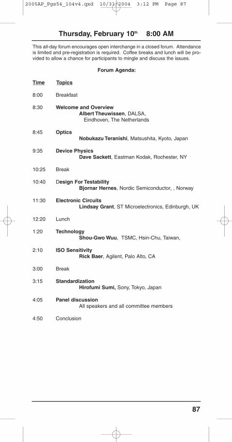
87
Thursday, February 10th 8:00 AM
This all-day forum encourages open interchange in a closed forum. Attendanceis limited and pre-registration is required. Coffee breaks and lunch will be pro-vided to allow a chance for participants to mingle and discuss the issues.
Forum Agenda:
Time Topics
8:00 Breakfast
8:30 Welcome and OverviewAlbert Theuwissen, DALSA,
Eindhoven, The Netherlands
8:45 OpticsNobukazu Teranishi, Matsushita, Kyoto, Japan
9:35 Device PhysicsDave Sackett, Eastman Kodak, Rochester, NY
10:25 Break
10:40 Design For TestabilityBjornar Hernes, Nordic Semiconductor, , Norway
11:30 Electronic CircuitsLindsay Grant, ST Microelectronics, Edinburgh, UK
12:20 Lunch
1:20 TechnologyShou-Gwo Wuu, TSMC, Hsin-Chu, Taiwan,
2:10 ISO SensitivityRick Baer, Agilent, Palo Alto, CA
3:00 Break
3:15 StandardizationHirofumi Sumi, Sony, Tokyo, Japan
4:05 Panel discussionAll speakers and all committee members
4:50 Conclusion
2005AP_Pgs54_104v4.qxd 10/31/2004 3:12 PM Page 87
88
CIRCUIT DESIGN FORUM
F4: Robust Design Solutions for Nanoscale Circuits:From DFM through End-of-Life
(Salon 7)
Organizers/Chair: Norman Rohrer, IBM, Essex Junction, VTCommittee: Atila Alvandpour, Linkoping University,
Linkoping, SwedenFumio Arakawa, Hitachi, Tokyo, JapanBill Bowhill, Intel, Hudson, MAHarry Fair, AMD, Boxborough, MAGeorgios Konstadinidis, Sun Micro.,
Sunnyvale, CANasser Kurd, Intel, Hillsboro, ORMargaret Martonosi, Princeton University,
Princeton, NJShannon Morton, Icera, Wiltshire, UKRon Preston, Intel, Hudson, MAAlice Wang, Texas Instruments, Dallas, TXC. K. Ken Yang, University of California,
Los Angeles, CA
65nm and 90nm technologies are putting the squeeze on CMOS circuitdesign. From DFM (birth) through reliability (end-of-life), the need forimproved modeling and design margin continues to expand. For example,the voltage range is limited at the upper end for hot electron effects andgate oxide reliability, while the lower voltages are limited by functionalityand SRAM stability. This forum will address DFM, reliability, design tools,design styles and architecture so your circuit may "live happily ever after".
Design for manufacturability (DFM) is a requirement for lithography. CliveBittlestone will address the issues and methods of analysis of OPC data.Ron Bolam will provide the nanoscale reliability mechanisms and trendsfor hot-electron effect, NBTI, gate oxide reliability and electromigration per-tinent to circuit design.
Jack Pippin will focus on the tools and techniques of circuit analysisrequired to optimize circuits within the reliability constraints. DavidGreenhill will show which circuit design styles are the most robust acrossthe life of the circuit. Hyun-Geun Byun will focus on SRAM reliability andmethods to cover SER and low voltage stability. Included with the SRAMdiscussion will be a new cell and the methods of testing.
High speed I/O design issues include the use of logic devices and increas-ing demand for higher data rates. Gerry Talbot will present solutions andmethods for analysis for 65nm technologies. Hisashige Ando will presentarchitectures which are tolerant to failures-in-time in SRAM and logicalfunctions.
Join us for a full day of expert analysis and presentation.
2005AP_Pgs54_104v4.qxd 10/31/2004 3:12 PM Page 88
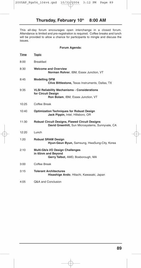
89
Thursday, February 10th 8:00 AM
This all-day forum encourages open interchange in a closed forum.Attendance is limited and pre-registration is required. Coffee breaks and lunchwill be provided to allow a chance for participants to mingle and discuss theissues.
Forum Agenda:
Time Topic
8:00 Breakfast
8:30 Welcome and OverviewNorman Rohrer, IBM, Essex Junction, VT
8:45 Modelling DFMClive Bittlestone, Texas Instruments, Dallas, TX
9:35 VLSI Reliability Mechanisms - Considerations for Circuit Design
Ron Bolam, IBM, Essex Junction, VT
10:25 Coffee Break
10:40 Optimization Techniques for Robust DesignJack Pippin, Intel, Hillsboro, OR
11:30 Robust Circuit Designs, Flawed Circuit DesignsDavid Greenhill, Sun Microsystems, Sunnyvale, CA
12:20 Lunch
1:20 Robust SRAM DesignHyun-Geun Byun, Samsung, HwaSung-City, Korea
2:10 Multi-Gb/s I/O Design Challenges in 65nm and Beyond
Gerry Talbot, AMD, Boxborough, MA
3:00 Coffee Break
3:15 Tolerant ArchitecturesHisashige Ando, Hitachi, Kawasaki, Japan
4:05 Q&A and Conclusion
2005AP_Pgs54_104v4.qxd 10/31/2004 3:12 PM Page 89
90
ATAC FORUMF5: ATAC: Automotive Technology and Circuits
(Salon 8)
Organizers/Chair: Herman Casier, AMI Semiconductor, Oudenaarde, Belgium
Wolfgang Pribyl, CONPRI, Graz, Austria Committee: Larry De Vito, Analog Devices, Wilmington, MA
Muneo Fukaishi, NEC, Kanagawa, Japan Franz Dielacher, Infineon, Villach, AustriaDieter Draxelmayr, Infineon, Villach, Austria Masayuki Katakura, SONY, Kanagawa, Japan David Robertson, Analog Devices, Wilmington, MA
While the automotive market has long been driven by innovations andimprovements of the mechanical, hydraulic and pneumatic systems of thecar, this situation has changed and the majority of innovations in cars areactually driven by electronics. Electronics will become even more perva-sive for the foreseeable future with a shift from separate electronic mod-ules, to fully interconnected intelligent systems e.g. X-by-wire.
This evolution, together with the growing use of high-performance sensorsrequires increasingly complex and accurate electronic hardware and soft-ware in the car. At the same time, the stringent safety requirements are fur-ther tightened and the harsh automotive environment demands are furtherincreased.
This Forum discusses the evolution in automotive high voltage and highpower technologies, complex system developments and robust circuitdesign.
In the first paper, a comprehensive overview of automotive electronic sys-tems and market trends will be given. The paper will demonstrate the keyelements needed for this evolution/revolution of automotive electronics.
The second and third papers will discuss semiconductor technologies forautomotive applications from the viewpoints of the car manufacturer andthe semiconductor industry.
In the fourth and fifth papers, complex system design issues and trade-offsfor in-vehicle image processing will be discussed. The use of such imageprocessing and secure data communication in the harsh automotive envi-ronment are important for driver assistance systems and therefore will gethigh attention.
The sixth, seventh and eight papers will focus on robust circuit designaspects for a Local Interconnect Network (LIN) transceiver, for current andfuture lighting systems in the car and for integrated magnetic field and sur-face micro machined pressure sensors.
At the end of the afternoon, all speakers will assemble in a panel formatfor an open discussion with the audience on the challenges in all aspectsof automotive electronics.
2005AP_Pgs54_104v4.qxd 10/31/2004 3:12 PM Page 90

91
Thursday, February 10th 8:00 AM
This all-day forum encourages open interchange in a closed forum. Attendanceis limited and pre-registration is required. Coffee breaks and lunch will be pro-vided to allow a chance for participants to mingle and discuss the issues.
Forum Agenda:
Time Topic
08:00 Continental Breakfast
08:30 Welcome and Introduction Herman Casier, AMIS, Oudenaarde, Belgium
08:40 Automotive Systems and Markets Patrick Leteinturier, Infineon, Munich, Germany
09:20 Semiconductor Technologies Support New Generation Hybrid Car
Masayuki Hattori, Toyota, Japan
10:00 SMARTMOS, the Ultimate Power, Analog,Mixed Signal Technology for Automotive Applications
Hak-Yam Tsoi, Freescale
10:40 Break
11:00 In Vehicle Image Processing LSI for Driver Assistant SystemsShorin Koy, NEC, Japan
11:40 Overview and Challenges of Data Communication in the Vehicle
Stefan Poledna, TTTech, Vienna, Austria
12:20 Lunch
01:40 A LIN transceiver, a case study of automotive design Koen Appeltans, AMIS, Oudenaarde, Belgium
02:20 Future Lighting Systems for Vehicles Gunther Leising, Lumitech, Austria
03:00 Smart Sensors for Automotive Applications Dirk Hammerschmidt, Infineon, Villach, Austria
03:40 Break
04:00 Panel Discussion
05:00 Conclusion
2005AP_Pgs54_104v4.qxd 10/31/2004 3:12 PM Page 91
92
INFORMATION
CONFERENCE REGISTRATION
ISSCC offers online registration. This is the fastest, most convenient wayto register and will give you immediate confirmation of whether or not youhave a place in the Tutorial and Short Course sessions of your choice, aswell as in any of the five Forums offered. If you register online using a cred-it card, your registration is processed while you are online, and your writ-ten confirmation can be downloaded and printed for your recordkeeping. Ifyou register by fax or mail, you will not receive confirmation for severaldays. Registration forms received without full payment will not beprocessed until payment is received at Event Solutions.
To register online, go to the ISSCC website at www.isscc.org/isscc or godirectly to the registration website at www.yesevents.com/isscc/index.asp.All payments must be made in U.S. Dollars, by credit card or check.Checks must be made payable to “ISSCC 2005”. Payments by credit cardwill appear on your monthly statement as a charge from ISSCC.
For those who wish to register by fax or mail, the Advance RegistrationForm can be found at the center of this booklet. Please read the explana-tions and instructions on the back of the form carefully.
The deadline for receipt of Early Registration fees is December 24, 2004.After December 24, 2004 and on or before January 11, 2005, registra-tions will be processed only at the Late Registration rates. As of January11, 2005 you must pay the onsite/highest registration fees. Because oflimited seating capacity in the meeting rooms and hotel fire regulations,onsite registration may be limited. Therefore, you are urged to registerearly to ensure your participation in all aspects of ISSCC 2005.
Full conference registration includes one copy each of the Digest ofTechnical Papers in both hard copy and on CD, the Visuals Supplement(mailed in March) and the ISSCC 2005 DVD that includes the Digest andVisuals (mailed in May). Student registration does not include theVisuals Supplement or the ISSCC 2005 DVD. All students must presenttheir Student ID at the Conference Registration Desk to receive the stu-dent rate. Anyone registering at the IEEE Member rate must also providehis/her IEEE Membership number. Those individuals who are members ofboth IEEE and SSCS will also receive a complimentary copy of the SSCSDigital Archive DVD set for years through 2004.
The On-site and Advance Registration Desks at ISSCC 2005 will be locat-ed in the Yerba Buena Ballroom Foyer at the San Francisco Marriott. Allparticipants, except presenting authors, must pick up their registrationmaterials at these desks as soon as they arrive at the hotel. ThePresenting Author for each paper must go directly to Golden Gate A3to register and to collect his/her materials.
REGISTRATION HOURS:Saturday, February 5 4:00 PM to 7:00 PM
(Tutorial and Forum Attendees Only)Sunday, February 6 6:30 AM to 1:30 PM
(Tutorial and Forum Attendees Only)4:00 PM to 8:00 PM
Monday, February 7 6:30 AM to 3:00 PMTuesday, February 8 8:00 AM to 3:00 PMWednesday, February 9 8:00 AM to 12:00 NoonThursday, February 10 7:00 AM to 1:00 PM
(Short Course and Forum Attendees Only)
2005AP_Pgs54_104v4.qxd 10/31/2004 3:12 PM Page 92

93
INFORMATION
NEXT ISSCC DATES AND LOCATIONISSCC 2006 will be held on February 5-9, 2006 at the San Francisco MarriottHotel.
FURTHER INFORMATIONPlease visit the ISSCC website at www.isscc.orgTo be placed on the Conference Mailing List, please contact the ConferenceOffice, c/o Courtesy Associates,
2025 M Street, N.W., Suite 800, Washington, DC 20036Email: [email protected]: 202-973-8722
HOTEL RESERVATIONSISSCC participants are urged to make their hotel reservations online.To do this,go to the conference website at www.isscc.org and click on the HotelReservation link to the San Francisco Marriott. In order to receive the specialgroup rates you will need to enter the following Group Codes: IEIIEIA for a sin-gle; IEIIEIB for a double; IEIIEIC for a triple; or IEIIEID for a quad. The specialISSCC group rates are $199/single; $219/double; $239/triple; and $259/quad.The dates of your reservation must fall within the period of February 4-10, 2005.All online reservations require the use of a credit card. Online reservations areconfirmed immediately, while you are online. We suggest that you print the pagecontaining your confirmation number and reservation details and bring it withyou when you travel to ISSCC. Once made and confirmed, your online reser-vation can be changed by calling the Marriott at 1-800-228-9290 (toll free) or415-896-1600, or by faxing your change to the Marriott at 415-442-0141.
For those who wish to make hotel reservations by fax or mail, the HotelReservation Form can be found in the center of this booklet. Be sure to fill inyour correct email address and fax number if you wish to receive a confirma-tion by email or fax.
Reservations must be received at the San Francisco Marriott no later thanJanuary 11, 2005 to obtain the special ISSCC rates. A limited number of roomsare available at these rates. Once this limit is reached and/or after January11th, the group rate will no longer be available. After the 11th, reservationrequests will be filled at the best available rate.
IMPORTANT NOTICE FOR ALL 2005 ISSCC PARTICPANTS: It is vitallyimportant that all 2005 ISSCC participants who do not live within drivingdistance of San Francisco make their hotel room reservations at the SanFrancisco Marriott, which is the conference hotel and location of all tech-nical sessions and all other conference activities. The room rates havebeen negotiated based upon our need to use all available meeting space in thehotel. If we do not fill our negotiated room block, the ISSCC must pay huge feesfor using all of the space. This will then result in unnecessary and unpopularincreases in registration fees for ISSCCC in future years. Please support theExecutive Committee in their attempt to keep your ISSCC registration fees rea-sonable. Book your room at the San Francisco Marriott hotel for ISSCC 2005.
CONFERENCE PUBLICATIONSAdditional ISSCC 2005 publications can be purchased at the ConferenceRegistration Desk. Prices are lower for purchases collected onsite than forthose publications ordered after the Conference that must be shipped to thepurchaser for an additional fee. Following ISSCC 2005, please order publi-cations directly from the publisher, [email protected].
TECHNICAL BOOK DISPLAY AND DAC STUDENT POSTERSA number of technical publishers will have a collection of professional booksand textbooks on display during the Conference. These books are available forsale or to order onsite. The book display is in the Golden Gate Hall, located onelevel above the ballroom and technical sessions. The Book Display will be openon Monday from 12:00Noon - 8:00PM; on Tuesday from 10:00AM to 8:00PM;and on Wednesday from 10:00AM to 5:00PM.
The DAC Student Poster Contest winners for 2004 and 2005 will also displaytheir winning papers in this area during the book display hours. AuthorInterviews will be held here as well, on Monday and Tuesday. Please note thatthe Author Interviews will move to the South Grand Assembly on Wednesday.
2005AP_Pgs54_104v4.qxd 10/31/2004 3:12 PM Page 93
94
INFORMATION
SSCS DIGITAL-ARCHIVE DVD SET
All ISSCC registrants who are members of the IEEE Solid-State Circuits
Society will receive a complementary SSCS Digital-Archive DVD Set. The
two-DVD set contains the IEEE Journal of Solid-State Circuits
(1966-2004), the conference records of the ISSCC (1955-2004), and the
Symposium on VLSI Circuits (1988-2004). In addition, new for this year,
the Digital-Archive DVD set will contain the conference records of the
Custom Integrated Circuits Conference (1988-2004) and the European
Solid-State Circuits Conference (1997-2004).
o To add SSCS membership while renewing IEEE membership,
go to www.ieee.org/renew
o To add SSCS membership after renewing IEEE membership, go
to www.ieee.org/addservices
o To join IEEE and SSCS, go to www.ieee.org/join
Check-off boxes are provided on the registration form to order additional
copies of the Digital-Archive DVD.
CD OF THE ISSCC DIGEST,
AND DVD OF THE DIGEST AND SLIDE SUPPLEMENT
New for this year, Conference attendees will receive a complementary CD
of the ISSCC 2005 Digest of Technical Papers, in addition to the printed
Digest, at the Conference. This CD will allow easy access to an
electronic version of the technical papers. In addition, all Conference
attendees (except student registrants) will receive by mail a complemen-
tary DVD containing the ISSCC 2005 Digest of Technical Papers, and the
ISSCC 2005 Visuals Supplement. This DVD will be mailed in May, 2005.
ISSCC 2004 and 2005 SHORT-COURSE DVDs
A DVD of the ISSCC 2004 Short Course, "Deep-Submicron Analog and
RF Circuit Design", and a DVD of the ISSCC 2005 Short Course,
"RF CMOS Circuits" will be available for purchase at the Conference.
These DVDs contain an audio recording of the original presentation,
synchronized with the slides, along with written textual transcript. In
addition, the DVD's will contain a pdf of the presentations suitable for
printing, along with pdfs of key reference material. Check-off boxes are
provided on the registration form to purchase the DVDs; They will not be
available for purchase after the Conference.
2005AP_Pgs54_104v4.qxd 10/31/2004 3:12 PM Page 94
95
COMMITTEES
EXECUTIVE COMMITTEE
Chair: Timothy Tredwell, Eastman Kodak Rochester, NY
Executive Dir.: Dave Pricer, Charlotte, VTExecutive Sec.: Frank Hewlett, Jr., Sandia National
Laboratories, Albuquerque, NMDirector of Finance: John Kennedy, Howard Hughes Medical
Institute, Palo Alto, CAProgram Chair: Ian Young, Intel, Hillsboro, ORProg. Vice Chair: Jan Sevenhans, LEA Asics for Broadband
Communications, Antwerpen, BelgiumProgram Sec.: Jan van der Spiegel, University of
Pennsylvania, Philadelphia, PAFar East Chair: Kunihiko Iizuka, Sharp, Nara, JapanFar East Vice Chair.: Jinyong Chung, Pohang University of Science
and Technology, Kyungbuk, KoreaFar East Secretary: Takayuki Kawahara, Hitachi, Tokyo, JapanEuropean Chair: Albert Theuwissen, DALSA,
Eindhoven, The NetherlandsEuropean Vice Chair: Rudolf Koch, Infineon Technologies,
Munich, GermanyEuropean Sec.: Qiuting Huang, Swiss Federal Institute of
Technology, Zürich, SwitzerlandTD Subcommittee Chair: Anantha Chandrakasan, Massachusetts
Institute of Technology, Cambridge, MATD Steering Com.: Yoshiaki Hagiwara, Sony, Tokyo, JapanShort Course: Terri Fiez, Oregon State University,
Corvallis, ORTutorials & Forums/Long-Range Planning Chair:
Willy Sansen, Katholieke Universiteit Leuven, Leuven, Belgium
Dir. of Publications/Presentations:Laura Fujino, University of Toronto,
Toronto, CanadaPress/Awards: Kenneth C. Smith, University of Toronto,
Toronto, CanadaDir. of Operations: Diane Melton, Courtesy Associates,
Washington, D.C.Digest Editors: Mandana Amiri, University of British Columbia,
Vancouver, CanadaArvin Grabel, Northeastern University
Boston, MAShahriar Mirabbasi, University of British
Columbia, Vancouver, CanadaRichard Spencer, University of California,
Davis, CACoordinator of Audio/Visual Services:
John Trnka, IBM, Rochester, MN
Liaison Members of Representatives:
Europe: Jan van der Spiegel, Univeristy of Pennsylvania, Philadelphia, PA
IEEE SSC Society: Bryan Ackland, Old Bridge, NJIEEE SSC Society: Gary Baldwin, University of California,
Berkeley, CAIEEE Bay Area Council: Robert P. TuIEEE San Francisco Section: James B. Lekas
International Technical Program Committee
Program Chair: Ian Young, Intel, Hillsboro, ORProg. Vice Chair: Jan Sevenhans, LEA ASICs for Broadband
Communications, Antwerp, BelgiumSecretary: Jan van der Spiegel, University of
Pennsylvania, Philadelphia, PA
2005AP_Pgs54_104v4.qxd 10/31/2004 3:12 PM Page 95
96
COMMITTEES
Analog Subcommittee:David Robertson, Chair, Analog Devices, Wilmington, MAAndrea Baschirotto, University of Lecce, Lecce, ItalyKlaas Bult, Broadcom Netherlands Bunnik, The NetherlandsZhongyuan Chang, IDT-Newave Technology, Shanghai, ChinaDieter Draxelmayr, Infineon, Villach, AustriaVenu Gopinathan, Irvine, CAKunihiko Iizuka, Sharp, Nara, JapanDavid Johns, University of Toronto, Toronto, CanadaRoy Scott Kaller, SMSC, Phoenix, AZMasayuki Katakura, Sony, Kanagawa, JapanBang Won Lee, ATLab Inc., KyungGi-Do, Korea Philip K.T. Mok, Hong Kong University of Science and Technology,
Hong Kong, ChinaBram Nauta, University of Twente, Enschede, The NetherlandsRobert Neff, Agilent Technologies, Palo Alto, CAAli M. Niknejad, University of California, Berkeley, CABill Redman-White, Philips, Southhampton, UKRaf Roovers, Philips, Eindhoven, The NetherlandsWilly Sansen, Katholieke Universiteit Leuven, BelgiumAxel Thomsen, Silicon Laboratories, Austin, TX
Digital Subcommittee:William Bowhill, Chair, Intel, Hudson, MAAtila Alvandpour, Linköping University, Linköping, SwedenFumio Arakawa, Hitachi, Tokyo, JapanDennis Fischette, AMD, Sunnyvale, CAHerbert Knapp, Infineon, Munich, Germany Peter Kogge, University of Notre Dame, Notre Dame, INGeorgios Konstadinidis, Sun Microsystems, Sunnyvale, CAChen-Yi Lee, National Chiao Tung University, Hsinchu, TaiwanMargaret Martonosi, Princeton University, Princeton, NJSouichi Miyata, Sharp, Nara JapanMasayuki Mizuno, NEC, Kanagawa, JapanShannon Morton, Icera, Bristol, UKSamuel Naffziger, Hewlett Packard, Fort Collins, COSung Park, Samsung, Gyengg, KoreaNorman Rohrer, IBM, Essex Junction, VTHector Sanchez, Freescale Semiconductor, Austin, TXHannu Tenhunen, Royal Institute of Technology, Kista, Sweden Jim Warnock, IBM, Yorktown Heights, NYThucydides Xanthopoulos, Cavium Networks, Marlboro, MAC.K. Ken Yang, University of California, Los Angeles, CAHoi-Jun Yoo, KAIST, Daejon, Korea
Imagers, Displays, and MEMS Subcommittee:Daniel McGrath, Chair, Eastman Kodak, Rochester, NYFarrokh Ayazi, Georgia Institute of Technology, Atlanta, GANavakanta Bhat, Indian Institute of Science, Bangalore, IndiaAbbas El Gamal, Stanford University, Stanford, CARalph Etienne-Cummings, Johns Hopkins University, Baltimore, MDBoyd Fowler, Agilent Technologies, Santa Clara, CARoberto Guerrieri, Università di Bologna, Bologna, ItalyHiroshi Hayama, NEC, Kanagawa, JapanJed Hurwitz, ST Microelectronics, Edinburgh, ScotlandMakoto Ikeda, University of Tokyo, Tokyo, JapanHirofumi Sumi, Sony, Kanagawa, JapanAlbert Theuwissen, DALSA, Eindhoven, The NetherlandsRoland Thewes, Infineon Technologies, Munich, GermanyEuisik Yoon, KAIST, Daejeon, KoreaTiemin Zhao, Reflectivity, Sunnyvale, CA
2005AP_Pgs54_104v4.qxd 10/31/2004 3:12 PM Page 96
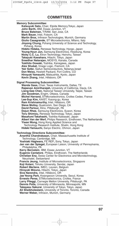
97
COMMITTEES
Memory Subcommittee:Katsuyuki Sato, Chair, Elpida Memory,Tokyo, JapanJohn Barth, IBM, Essex Junction, VTBruce Bateman, T-RAM, San Jose, CAMark Bauer, Intel, Folsom, CAMartin Brox, Infineon Technologies, Munich, GermanyGiulio Casagrande, ST Microelectronics, Milano, ItalyJinyong Chung, Pohang University of Science and Technology,
Pohang, KoreaHideto Hidaka, Renesas Technology, Hyogo, JapanYoung-Hyun Jun, Samsung Electronics, HwaSung, KoreaNicky C.C. Lu, Etron Technology, Hsinchu, TaiwanTakayuki Kawahara, Hitachi, Tokyo, JapanSreedhar Natarajan, MOSYS, Kanata, CanadaYukihito Oowaki, Toshiba, Kanagawa, JapanAlex Shubat, Virage Logic, Fremont, CAYair Sofer, Saifun Semiconductors, Netanya,IsraelDon Weiss, Hewlett Packard, Fort Collins, COHiroyuki Yamauchi, Matsushita, Kyoto, JapanKevin Zhang, Intel, Hillsboro, OR
Signal Processing Subcommittee:Wanda Gass, Chair, Texas Instruments, Dallas, TXRajeevan Amirtharajah, University of California, Davis, CALiang-Gee Chen, National Taiwan University, Taipei, TaiwanJim Goodman, Engim, Ottawa, CanadaMichel Harrand, STMicroelectronics, Crolles Cedex, FranceLee-Sup Kim, KAIST, Yusong-gu, KoreaRam Krishnamurthy, Intel, Hillsboro, ORSteve Molloy, Qualcomm, San Diego, CADavid Parlour, Xlinx, Pittsburgh, PADojun Rhee, Samsung Electronics, Suwon, KoreaToru Shimizu, Renesas Technology, Tokyo, JapanMasafumi Takahashi, Toshiba Kawasaki, JapanAlbert Van der Werf, Philips Research, Eindhoven, The NetherlandsYiwan Wong, Hong Kong Applied Science and
Technology Research Institute, Shatin, Hong KongHideki Yamauchi, Sanyo Electric, Ohmori, Japan
Technology Directions Subcommittee:Anantha Chandrakasan, Chair, Massachusetts Institute of
Technology, Cambridge, MAYoshiaki Hagiwara, FE REP, Sony, Tokyo, JapanJan van der Spiegel, European Laison, University of Pennsylvania,
Philadelphia, PAKerry Bernstein, IBM, Essex Junction, VTEugenio Cantatore, Philips, Eindhoven, The NetherlandsChristian Enz, Swiss Center for Electronics and Microtechnology,
Neuchatel, SwitzerlandFrancis Jeung, Institute of Microelectronics, SingaporeKoji Kotani, Tohoku University, Sendai, JapanRobert Mertens, IMEC, Leuven, BelgiumHiroyuki Mizuno, Hitachi, Tokyo, JapanSiva Narendra, Intel, Hillsboro, ORJae Yeong Park, Kwangwoon University, Seoul, KoreaErnesto Perea, STMicroelectronics, Crolles, FranceLarry Pileggi, Carnegie Mellon University, Pittsburgh, PADennis Polla, University of Minnesota, Minneapolis, MNTakayasu Sakurai, University of Tokyo, Tokyo, JapanAli Sheikholeslami, University of Toronto, Toronto, CanadaWerner Weber, Infineon, Munich, Germany
2005AP_Pgs54_104v4.qxd 10/31/2004 3:12 PM Page 97
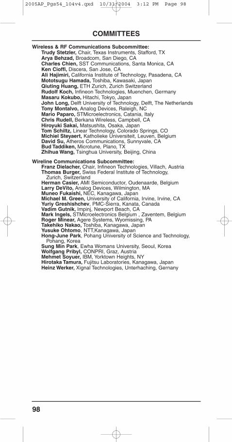
98
COMMITTEES
Wireless & RF Communications Subcommittee:Trudy Stetzler, Chair, Texas Instruments, Stafford, TXArya Behzad, Broadcom, San Diego, CACharles Chien, SST Communications, Santa Monica, CAKen Cioffi, Discera, San Jose, CAAli Hajimiri, California Institute of Technology, Pasadena, CAMototsugu Hamada, Toshiba, Kawasaki, JapanQiuting Huang, ETH Zurich, Zurich SwitzerlandRudolf Koch, Infineon Technologies, Muenchen, GermanyMasaru Kokubo, Hitachi, Tokyo, JapanJohn Long, Delft University of Technology, Delft, The NetherlandsTony Montalvo, Analog Devices, Raleigh, NCMario Paparo, STMicroelectronics, Catania, ItalyChris Rudell, Berkana Wireless, Campbell, CAHiroyuki Sakai, Matsushita, Osaka, JapanTom Schiltz, Linear Technology, Colorado Springs, COMichiel Steyaert, Katholieke Universiteit, Leuven, BelgiumDavid Su, Atheros Communications, Sunnyvale, CABud Taddiken, Microtune, Plano, TXZhihua Wang, Tsinghua University, Beijing, China
Wireline Communications Subcommittee:Franz Dielacher, Chair, Infineon Technologies, Villach, AustriaThomas Burger, Swiss Federal Institute of Technology,
Zurich, SwitzerlandHerman Casier, AMI Semiconductor, Oudenaarde, BelgiumLarry DeVito, Analog Devices, Wilmington, MAMuneo Fukaishi, NEC, Kanagawa, JapanMichael M. Green, University of California, Irvine, Irvine, CAYuriy Greshishchev, PMC-Sierra, Kanata, CanadaVadim Gutnik, Impinj, Newport Beach, CAMark Ingels, STMicroelectronics Belgium , Zaventem, BelgiumRoger Minear, Agere Systems, Wyomissing, PATakehiko Nakao, Toshiba, Kanagawa, JapanYusuke Ohtomo, NTT,Kanagawa, JapanHong-June Park, Pohang University of Science and Technology,
Pohang, KoreaSung Min Park, Ewha Womans University, Seoul, KoreaWolfgang Pribyl, CONPRI, Graz, AustriaMehmet Soyuer, IBM, Yorktown Heights, NYHirotaka Tamura, Fujitsu Laboratories, Kanagawa, JapanHeinz Werker, Xignal Technologies, Unterhaching, Gernany
2005AP_Pgs54_104v4.qxd 10/31/2004 3:12 PM Page 98
99
COMMITTEES
EUROPEAN REGIONAL COMMITTEE
Chair: Albert Theuwissen, DALSA, Eindhoven, The Netherlands
Vice-Chair: Rudolf Koch, Infineon Technologies Munich, Germany
Secretary: Qiuting Huang, Swiss Federal Institute of Technology, Zurich, Switzerland
Members:Atila Alvandpour, Linköping University, Linköping, SwedenAndrea Baschirotto, University of Lecce, Lecce, ItalyMartin Brox, Infineon, Munich, GermanyKlaas Bult, Broadcom, Bunnik, The NetherlandsThomas Burger, ETH, Zurich, SwitzerlandEugenio Cantatore, Philips, Eindhoven,
The NetherlandsGiulio Casagrande, ST Microelectronics, Milano, ItalyHerman Casier, AMI Semiconductor, Oudenaarde, BelgiumFranz Dielacher, Infineon, Villach, AustriaDieter Draxelmayr, Infineon, Villach, AustriaChristian Enz, Swiss Center for Electronics and Microtechnology,
Neuchatel, SwitzerlandRoberto Guerrieri, Università di Bologna, Bologna, ItalyMichel Harrand, STMicroelectronics, Crolles Cedex, FranceJed Hurwitz, STMicroelectronics, Edinburgh, ScotlandMark Ingels, STMicroelectronics, Zaventem, BelgiumHerbert Knapp, Infineon, Munich, GermanyJohn Long, Delft University of Technology, Delft, The NetherlandsRobert Mertens, IMEC, Leuven, BelgiumBram Nauta, MESA+ Research Institute, Enschede,
The NetherlandsMario Paparo, STMicroelectronics, Catania, ItalyErnesto Perea, STMicroelectronics, Crolles, FranceWolfgang Pribyl, Austria Mikro Systems, Unterpremstatten, AustriaBill Redman-White, Philips, Southampton, UKRaf Roovers, Philips, Eindhoven, The NetherlandsWilly Sansen, Katholieke Universiteit Leuven, Leuven, BelgiumJan Sevenhans, LEA Asics for Broadband
Communications, Antwerpen, BelgiumYair Sofer, Saifun Semiconductors, Netanya,IsraelMichiel Steyaert, Katholieke Universiteit Leuven, BelgiumHannu Tenhunen, Kungl Tekniska Hogskolan, Kista, SwedenRoland Thewes, Infineon, Munich, GermanyAlbert van der Werf, Philips, Eindhoven, The NetherlandsWerner Weber, Infineon, Munich, GermanyHeinz Werker, Xignal Technologies, Unterhaching, Gernany
2005AP_Pgs54_104v4.qxd 10/31/2004 3:12 PM Page 99
100
COMMITTEES
FAR-EAST REGIONAL COMMITTEE
Chair: Kunihiko Iizuka, Sharp, Nara, JapanVice Chair: Jinyong Chung, Pohang University of Science
and Technology, Pohang, KoreaSecretary: Takayuki Kawahara, Hitachi, Tokyo Japan
Members:Fumio Arakawa, Hitachi, Tokyo, JapanNavakanta Bhat, Indian Institute of Science, Bangalore, IndiaZhongyuan Chang, IDT-Newave Technology, Shanghai, ChinaLiang-Gee Chen, National Taiwan University, Taipei, TaiwanMuneo Fukaishi, Kanagawa, JapanYoshiaki Hagiwara, REP, Sony, Tokyo, JapanMototsugu Hamada, Toshiba, Stanford, CAHiroshi Hayama, NEC , Kanagawa, JapanHideto Hidaka, Renesas Technology, Hyogo, JapanMakoto Ikeda, University of Tokyo, Tokyo, JapanFrancis YC Jeung, Institute of Microelectronics, SingaporeYoung-Hyun Jun, Samsung Electronics, HwaSung-City, KoreaMasayuki Katakura, Sony, Kanagawa, JapanLee-Sup Kim, KAIST, Daejeon, KoreaMasaru Kokubo, Hitachi, Tokyo, JapanKoji Kotani, Tohoku University, Sendai, JapanChen-Yi Lee, National Chiao Tung University, Hsinchu, TaiwanBang Won Lee, ATLab, KyungGi-Do, Korea Nicky C.C. Lu, Etron Technology, Hsinchu, TaiwanSouichi Miyata, Sharp, Nara JapanHiroyuki Mizuno, Hitachi, Tokyo, JapanMasayuki Mizuno, NEC, Kanagawa, JapanPhilip K.T. Mok, Hong Kong University, Kowloon, ChinaTakehiko Nakao, Toshiba, Kanagawa, JapanYusuke Ohtomo, NTT,Kanagawa, JapanYukihito Oowaki, Toshiba, Kanagawa, JapanHong-Jung Park, POSTECH, Kyungbuk, KoreaJae Yeong Park, LG Electronics Institute of Technology,
Seoul, KoreaSung Bae Park, Samsung Electronics, Yongin, KoreaSung Min Park, Ewha Womans University, Seoul, KoreaHiroyuki Sakai, Matsushita, Osaka, JapanTakayasu Sakurai, University of Tokyo, Tokyo, JapanKatsuyuki Sato, Elpida Memory, Tokyo, JapanToru, Shimizu, Renesas Technology, Tokyo, JapanHirofumi Sumi, Sony, Kanagawa, JapanMasafumi Takahashi, Toshiba Kawasaki, JapanHirotaka Tamura, Fujitsu Laboratories, Kanagawa, JapanZhihua Wang, Tsinghua University, Bejing, ChinaYiwan Wong, Hong Kong Applied Science and Technology Research
Institute, Shatin, Hong KongHideki Yamauchi, Sanyo, Gifu, JapanHiroyuki Yamauchi, Matsushita, Kyoto, JapanHoi-Jun Yoo, KAIST, Taejon, KoreaEuisik Yoon, KAIST, Daejeon, Korea
2005AP_Pgs54_104v4.qxd 10/31/2004 3:12 PM Page 100
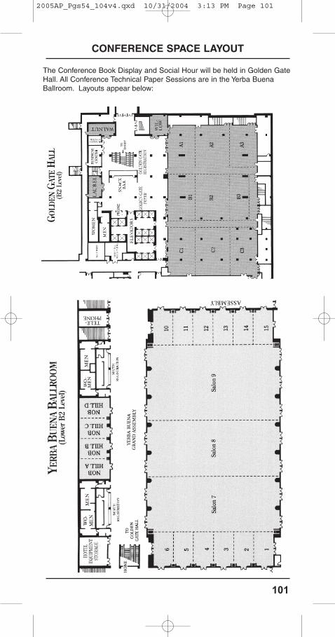
101
CONFERENCE SPACE LAYOUT
The Conference Book Display and Social Hour will be held in Golden GateHall. All Conference Technical Paper Sessions are in the Yerba BuenaBallroom. Layouts appear below:
2005AP_Pgs54_104v4.qxd 10/31/2004 3:13 PM Page 101
102
The simultaneous timing of papers given at ISSCC permits attendees tosession-hop from session to session without having to miss importantmaterial. This Advance Program provides you with the starting time foreach paper.
Taking pictures and videos during any of the sessions is not permitted.
A printed supplement with speakers' visuals will be mailed within onemonth of the conclusion of ISSCC 2005 to all registrants paying the fullmember or non-member Conference fees. A DVD containing both theISSCC 2005 Digest of Technical Papers and the Visuals Supplement willbe mailed in May to speakers and all attendees paying the full registrationfees.
Conference Information: Courtesy Associates Fax: 202-973-8722 email: [email protected]
Hotel Information: San Francisco Marriott 55 Fourth StreetSan Francisco, CA 9410 Telephone: 415-896-1600
Press Information: Kenneth C. Smith University of Toronto Phone: 416-978-5033 Fax: 416-971-2286email: [email protected]
Registration: Event Solutions UnlimitedP.O. Box 32862 Baltimore, MD 21282 Phone: 410-559-2236 or 1-800-937-8728 Fax: 410-559-2217 email: [email protected]
ISSCC Website: www.isscc.org/isscc
Make the most of your trip to San Francisco! Visit the San FranciscoConvention & Visitors Bureau Website at www.sfvisitor.org. To make yourtrip to the hotel easier, the Bay Area Rapid Transit (BART) SFO Extensionis open, offering a convenient means of transportation between the airportand the hotel. For additional information on reaching downtown SanFrancisco, visit BART's website at www.bart.gov.
For information on ground transportation, maps and driving directions,visit:
www.san-francisco-sfo.comwww.sfmarriott.com/travel/directions.aspx
ISSCC 2005 is sponsored by the IEEE Solid-State Circuits Society. Co-sponsors are the IEEE San Francisco Section and Bay Area Council, andthe University of Pennsylvania.
CONFERENCE INFORMATION
2005AP_Pgs54_104v4.qxd 10/31/2004 3:13 PM Page 102
2005AP_Pgs54_104v4.qxd 10/31/2004 3:13 PM Page 103
445 HO
ES
LAN
EP
O B
OX
1331P
ISC
ATAW
AY, NJ 08855-1331
ISS
CC
2005 AD
VAN
CE
PR
OG
RA
M
IEEE
2005AP_Pgs54_104v4.qxd 10/31/2004 3:13 PM Page 104