2002 microelectronics · diesel fuel-injection: an overview 1 987 722 104 3-934584-35-7 electronic...
TRANSCRIPT

ISBN-3-934584-49-7 The Bosch Yellow Jackets Edition 2001 Technical Instruction Automotive Electrical and Electronic SystemsOrder Number 1 987 722 122 AA/PDI-03.02-En
2002
Æ
AutomotiveMicroelectronics
Tech
nica
l Ins
truc
tion
Mic
roel
ectr
onic
s in
Mot
or V
ehic
les
The
Bos
ch Y
ello
w J
acke
ts
• Basic principles• Components• Development
and production
Automotive Technology
The Program Order Number ISBN
Automotive electrics/Automotive electronicsBatteries 1 987 722 153 3-934584-21-7Alternators 1 987 722 156 3-934584-22-5Starting Systems 1 987 722 170 3-934584-23-3Lighting Technology 1 987 722 176 3-934584-24-1Electrical Symbols and Circuit Diagrams 1 987 722 169 3-934584-20-9Automotive Sensors 1 987 722 131 3-934584-50-0Automotive Microelectronics 1 987 722 122 3-934584-49-7
Diesel-Engine ManagementDiesel Fuel-Injection: an Overview 1 987 722 104 3-934584-35-7Electronic Diesel Control EDC 1 987 722 135 3-934584-47-0Diesel Accumulator Fuel-Injection System Common Rail CR 1 987 722 175 3-934584-40-3Diesel Fuel-Injection Systems Unit Injector System/Unit Pump System 1 987 722 179 3-934584-41-1Radial-Piston Distributor Fuel-Injection Pumps Type VR 1 987 722 174 3-934584-39-XDiesel Distributor-Type Fuel-Injection Pumps VE 1 987 722 164 3-934584-38-1Diesel In-Line Fuel-Injection Pumps PE 1 987 722 162 3-934584-36-5Governors for Diesel In-Line Fuel-Injection Pumps 1 987 722 163 3-934584-37-3
Gasoline-Engine ManagementEmission Control (for Gasoline Engines) 1 987 722 102 3-934584-26-8Gasoline Fuel-Injection System K-Jetronic 1 987 722 159 3-934584-27-6Gasoline Fuel-Injection System KE-Jetronic 1 987 722 101 3-934584-28-4Gasoline Fuel-Injection System L-Jetronic 1 987 722 160 3-934584-29-2Gasoline Fuel-Injection System Mono-Jetronic 1 987 722 105 3-934584-30-6Spark Plugs 1 987 722 155 3-934584-32-2Ignition 1 987 722 154 3-934584-31-4M-Motronic Engine Management 1 987 722 161 3-934584-33-0ME-Motronic Engine Management 1 987 722 178 3-934584-34-9Gasoline-Engine Management: Basics and Components 1 987 722 136 3-934584-48-9
Driving and Road-Safety SystemsConventional Braking Systems 1 987 722 157 3-934584-42-XBrake Systems for Passenger Cars 1 987 722 103 3-934584-43-8ESP Electronic Stability Program 1 987 722 177 3-934584-44-6Compressed-Air Systems for Commercial Vehicles (1): Systems and Schematic Diagrams 1 987 722 165 3-934584-45-4Compressed-Air Systems for Commercial Vehicles (2): Equipment 1 987 722 166 3-934584-46-2Safety, Comfort and Convenience Systems 1 987 722 150 3-934584-25-XAudio, navigation, and telematics in the vehicle 1 987 722 132 3-934584-53-5
The up-to-date program is available in Internet under:www.bosch.de/aa/en/fachliteratur/index.htm www.cargeek.ir
www.CarGeek.ir
www.cargeek.ir

Published by:© Robert Bosch GmbH, 2002Postfach 30 02 20,D-70442 Stuttgart.Automotive Aftermarket Business Sector,Department AA/PDT5.Product Marketing,Diagnostics, Test Equipment.
Editor-in-chief:Dipl.-Ing. (FH) Horst Bauer.
Editorial team:Dipl.-Ing. (BA) Jürgen Crepin,Dipl.-Ing. Karl-Heinz Dietsche,Dipl.-Holzw. Folkhart Dinkler.
Authors:Dipl.-Ing. Adolf Fritz (Control Unit Development),Dr. rer. nat. Ulrich Goebel (Hybrid Circuit Board Production),Armin Hess (Example Circuit),Karlheinz Isert (Printed Circuit Board Production),Dr. rer. nat. Ulrich Schaefer (Basic Principles, Components, Microcontroller)
and the editorial team in co-operation with the responsible technical departments of Robert Bosch GmbH.
Unless otherwise stated, the above are all em-ployees of Robert Bosch GmbH, Stuttgart.
Reproduction, duplication, and translation of thispublication, including excerpts therefrom, is onlyto ensue with our previous written consent andwith particulars of source.Illustrations, descriptions, schematic diagrams,and other data only serve for explanatory pur-poses, and for presentation of the text. Theycannot be used as the basis for design, installa-tion, and scope of delivery. We undertake no lia-bility for conformity of the contents with nationalor local regulations.Robert Bosch GmbH is exempt from liability,and reserves the right to make changes at anytime.
Printed in Germany.Imprimé en Allemagne.
1st Edition, August 2001.English translation of the German edition dated:February 2001.(1.0)
Imprint
Robert Bosch GmbH
www.cargeek.ir
www.CarGeek.ir
www.cargeek.ir

Automotive microelectronics
Robert Bosch GmbH
Robert Bosch GmbH
www.cargeek.ir
www.CarGeek.ir
www.cargeek.ir

4 Automotive microelectronics4 Overview6 Demands on electronic systems6 History of development
8 Basic principles ofsemiconductor technology
8 Terminology8 Electrical conductivity
12 Electronic components12 Passive components13 Semiconductor components14 Diodes16 Semiconductor resistors17 Transistors20 Monolithic integrated circuits24 Microcomputers27 Semiconductor memories30 Opto-electronic components32 Micromechanical sensors
34 Microcontrollers34 Microcontroller developments36 Microcontroller components37 Microcontroller design and
operating concept41 Microcontroller memories42 Microcontroller peripheral modules44 Microcontroller busses
46 Circuit example 46 Overview48 Design and construction55 Operating concept58 Programming
60 ECU development60 Overview64 Hardware development
68 Manufacture of semiconductorcomponents and circuits
68 Semiconductor components72 Micromechanics73 Conventional printed-circuit
boards78 Film and hybrid circuits
80 Glossary and Tables forautomotive microelectronics
88 Index of technical terms91 Abbreviations
Contents
Robert Bosch GmbH
www.cargeek.ir
www.CarGeek.ir
www.cargeek.ir
Motor vehicles are now inconceivable without electronic control units and their associ-
ated sensors and actuators. Such components have revolutionised the automotive
world. All essential vehicle functions are electronically controlled by systems and com-
ponents that occupy only a tiny space. There are systems that control the function of
engine and gearbox, the safety and security systems and a large number of comfort and
convenience systems, and the number of “intelligent” vehicle systems is growing at a
rapid pace. Nor is there any foreseeable end to this trend.
Electronic control systems open the door to a vast array of possibilities. They im-
prove vehicle safety and ride comfort. At the same time, they make vehicles more
economical and kinder to the environment.
The triumphant advance of electronics has created a vocabulary of terms with
which we are bombarded every day. It is becoming more and more difficult to under-
stand what precisely those terms refer to.
This publication in the Bosch Yellow Jacket “Technical Instruction” series explains the
specialist terminology of microelectronics in detail.
It starts with a short introduction followed by an explanation of the principles of
semiconductor technology and how microelectronic components interact. A practical
example of a circuit helps to consolidate the theoretical concepts described. This is
then followed by a description of the development and production of control units.
Finally, the glossary provides a quick guide to the most important microelectronics
terms.
The functions of the individual electronic systems (e.g. MED, EDC, ESP) are described
in detail in separate publications in the Yellow Jacket “Technical Instruction” series.
Robert Bosch GmbH
www.cargeek.ir
www.CarGeek.ir
www.cargeek.ir

Microelectronics have revolutionised motorvehicle technology. Initially, mechanicalcomponents were replaced by electronicdevices in order to make systems morereliable. This was the case with the contactbreaker points in the conventional coil igni-tion system, for example. Gradually, how-ever, more and more new vehicle systemswere introduced which simply would nothave been possible without the use of elec-tronics. The impetus for these new develop-ments was provided by increasingly de-manding requirements placed on theexhaust-emission characteristics of theinternal-combustion engine (e.g. emission-control systems), on comfort and con-venience (e.g. climate control and naviga-tion systems) and on safety (e.g. antilockbraking system [ABS] and airbags).
Overview
Cars and commercial vehicles equipped with the latest available technical improvementsare absolutely brimming with electronic sys-tems. Those systems can be subdivided intothe following areas of application: Engine and drivetrain Safety Comfort and convenience Communication and multimedia.
Fig. 1 provides an overview of the electronicsystems that can be found on modern motorvehicles. Many of the systems referred to arenow standard equipment on all new vehi-cles. By contrast, there are others that re-main (as yet) the preserve of the most ex-pensive luxury models.
Electronic systems can be subdivided intothe following functional areas: Sensors and setpoint generators Control units (ECUs) Actuators ECU communication links (networks)
and Electronic diagnosis
Sensors and setpoint generators Sensors detect operating conditions (e.g. en-gine speed, wheel speed, temperature). Theyconvert physical variables into electrical sig-nals. Setpoint generators (e.g. controls oper-ated by the driver) specify desired settings.
Control units (ECUs)Control units process the information re-ceived from the sensors and setpoint gener-ators using specific mathematical calculationsequences (control algorithms). They con-trol the actuators by means of electrical out-put signals. Control units also form the in-terface with other systems and the vehiclediagnostics.
ActuatorsActuators convert the electrical output sig-nals from the control unit into physicalvariables. Examples of actuators are: gasoline-engine fuel injectors diesel-engine fuel injectors electric motors (e.g. for driving the
power-window regulator mechanism or asthrottle-valve positioner on vehicles withETC (Electronic Throttle Control))
fans
NetworksAs the number of electronic systems in vehi-cles grows, so does the amount of intercon-necting wiring needed. The total length ofthe wiring in the wiring harness of a mid-range car is now roughly 1.6 km on averageand incorporates up to 300 connectors witha total of around 2000 connector pins.
Networking of the various systems reducesthe overall length of the wiring required. Ashared data bus consisting of only two wires(e.g. CAN bus) carries data that is read by all bus users. Depending on the specific re-quirements, a vehicle may also have separatebusses for engine and drivetrain, comfortand convenience systems, and communica-tion systems.
4 Automotive microelectronics Overview
Automotive microelectronics
Robert Bosch GmbH
www.cargeek.ir
www.CarGeek.ir
www.cargeek.ir

Motor vehicles are now inconceivable without electronic control units and their associ-
ated sensors and actuators. Such components have revolutionised the automotive
world. All essential vehicle functions are electronically controlled by systems and com-
ponents that occupy only a tiny space. There are systems that control the function of
engine and gearbox, the safety and security systems and a large number of comfort and
convenience systems, and the number of “intelligent” vehicle systems is growing at a
rapid pace. Nor is there any foreseeable end to this trend.
Electronic control systems open the door to a vast array of possibilities. They im-
prove vehicle safety and ride comfort. At the same time, they make vehicles more
economical and kinder to the environment.
The triumphant advance of electronics has created a vocabulary of terms with
which we are bombarded every day. It is becoming more and more difficult to under-
stand what precisely those terms refer to.
This publication in the Bosch Yellow Jacket “Technical Instruction” series explains the
specialist terminology of microelectronics in detail.
It starts with a short introduction followed by an explanation of the principles of
semiconductor technology and how microelectronic components interact. A practical
example of a circuit helps to consolidate the theoretical concepts described. This is
then followed by a description of the development and production of control units.
Finally, the glossary provides a quick guide to the most important microelectronics
terms.
The functions of the individual electronic systems (e.g. MED, EDC, ESP) are described
in detail in separate publications in the Yellow Jacket “Technical Instruction” series.
Robert Bosch GmbH
www.cargeek.ir
www.CarGeek.ir
www.cargeek.ir

Another advantage of the bus system is thatsensor signals need only be analysed by asingle control unit. For example, the instru-ment cluster can use the individual wheel-speed signals delivered by the ABS controlunit to calculate the vehicle’s road speed.This complex calculation even takes accountof cornering differences and spinningwheels. The road-speed signal is transferredon the CAN bus to all other users (e.g. theABS control unit which uses it for control-ling brake application, the engine-manage-ment ECU which uses it as the basis forcruise control, or the car radio for the speed-related volume adjustment).
Electronic diagnosisElectronic diagnosis functions on the con-trol unit continuously monitor the opera-tion of the system and its components. Anyfaults that occur (e.g. short circuits in thewiring, sensor failure) are stored in the con-trol unit’s fault memory. Those stored faultscan then be read out in the course of serviceusing a dedicated system tester that is con-nected to the control unit’s diagnosis inter-face. The system tester can also be used toscan sensor signals and send commands toactuators to perform specific operations.Electronic diagnosis thus enables faults to belocated more quickly and easily in the courseof vehicle service.
Automotive microelectronics Overview 5
Elektronik im Kfz
Drivetr
ain
Commun
icatio
nEle
ctron
ic vo
ice ou
tput
Voice
contr
ol of
functi
ons
(spee
ch re
cogn
ition)
Audio
equip
ment (r
adio,
CD, e
tc.)
Video
On-boa
rd co
mputer
Car ph
one
Naviga
tion
New di
splay
tech
nolog
ies
(head
-up di
splay
)
Intern
et an
d PC
Bus s
ystem
(e.g.
CAN
)
Syste
m diag
nosis
Digital
engin
e man
agem
ent:
gaso
line e
ngine
: Motr
onic
Diesel
engin
e: Ele
ctron
ic
diese
l con
trol (E
DC)
with
electr
onica
lly co
ntroll
ed
fuel in
jectio
n,ele
ctron
ic ign
ition
(gaso
line e
ngine
),
Lambd
a exh
aust-
emiss
ion
contr
ol bo
ost-p
ressu
re
contr
ol, et
c. Ele
ctron
ic tra
nsmiss
ion-
shift
contr
ol On-b
oard
diagn
osis
(OBD
)
Contro
ller A
rea N
etwork
(CAN
)Sy
stem di
agno
sis
Cruise
contr
ol
Adap
tive c
ruise
contr
ol
(rada
r sen
sor)
Heatin
g and
air-c
ondit
ioning
Seat
adjus
tmen
t with
positi
on m
emory
Centra
l lock
ing
Adap
tive s
uspe
nsion
Revers
ing as
sistan
ce
Contro
ller A
rea N
etwork
(CAN
)
Syste
m diag
nosis
Antilo
ck br
aking
syste
m (ABS
)
Tracti
on co
ntrol
syste
m (TCS)
Electr
onic
stabili
ty pro
gram (E
SP)
Headla
mp adju
stmen
t an
d clea
ning
Litron
ic
Wash-w
ipe co
ntrol
Indivi
duali
sed s
ervice
interv
al dis
play
Monito
ring s
ystem
s for
cons
umab
les an
d
wearin
g par
ts
Trigg
ering
syste
ms for
airba
gs, s
eatbe
lt ten
sione
rs
and
roll-o
ver b
ar
Vehic
le se
curity
syste
ms
Tire-p
ressu
re mon
itorin
g
Contro
ller A
rea N
etwork
(CAN
)
Syste
m diag
nosis
bar
Safet
y
Comfor
t and
conv
enien
ce
Electronics in Motor Vehicles (Cars)1æ
UA
E08
56E
Robert Bosch GmbH
www.cargeek.ir
www.CarGeek.ir
www.cargeek.ir

Demands on electronicsystemsElectronic systems in motor vehicles areexposed to extreme stresses (e.g. due toextreme temperature variations, unusualclimatic conditions, poor road surfaces andthe effect of corrosive substances). These aresome of the requirements they must meet inorder to be able to function reliably andwithout faults over long periods: Resistance to temperatures ranging from
–40 °C ... 125 °C EMC (electromagnetic compatibility):
immunity to external interference (e.g.mobile phone signals) and no emission ofelectromagnetic radiation likely to causeinterference on other equipment
Resistance to shocks and vibration Resistance to water and damp Resistance to corrosive fluids (e.g. oils and
salt-water spray) Light weight Economical production costs and Secure and trouble-free mounting
History of development
The amount of electronic equipment inmotor vehicles is continually increasing.Fig. 2 provides an overview of the growth of electronic equipment expressed as a pro-portion of vehicle cost.
Because of their cost, electronic systemswere initially reserved for vehicles at the lux-ury end of the market. This explains why in1980 electronic equipment accounted foronly half a percent of vehicle cost. From thattime onwards, and particularly in the 1990s,that proportion grew rapidly as the price ofelectronic equipment continually droppedwith the result that more and more systemscould be fitted to mid-range and even smallcars.
Gradually, more and more electronic sys-tems were fitted to motor vehicles (Table 1).And the trend continues.
The new science of mechatronics dealswith the interaction between mechanical,electronic and data processing devices.
6 Automotive microelectronics Demands on electronic systems/History of development
Table 1
1980 1990
2000 2010Prognosis
0.5 % 7 %
17 % 24 %
Proportion of cost per vehicle (overall average)
2
æU
AE
0855
E
1958 DC generator with variode1962 3-phase alternator with variode1965 Transistorised ignition1967 D-Jetronic gasoline-injection system
(pressure-controlled)1978 Antilock braking system (ABS)1979 Motronic
(combined ignition and fuel-injection system)1982 Electronic ignition system1982 Knock control1986 Electronic diesel control (EDC)1986 Electronic throttle control (ETC)1987 Traction control system (TCS)1989 Electronic transmission-shift control
(“stand-alone” system Tiptronic)1989 CAN (Controller Area Network)1989 Vehicle navigation system (Travelpilot)1991 Litronic1994 ME-Motronic (integrated ETC)1997 Electronic stability program (ESP)2000 MED-Motronic (gasoline direct injection)2000 Adaptive Cruise Control
Historical development of electronic systems in motor vehicles (examples)
1
Robert Bosch GmbH
www.cargeek.ir
www.CarGeek.ir
www.cargeek.ir
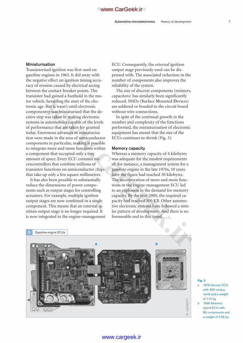
MiniaturisationTransistorised ignition was first used ongasoline engines in 1965. It did away withthe negative effect on ignition timing accu-racy of erosion caused by electrical arcingbetween the contact-breaker points. Thetransistor had gained a foothold in the mo-tor vehicle, heralding the start of the elec-tronic age. But is wasn’t until electroniccomponentry was miniaturised that the de-cisive step was taken in making electronicsystems in automobiles capable of the levelsof performance that are taken for grantedtoday. Enormous advances in miniaturisa-tion were made in the area of semiconductorcomponents in particular, making it possibleto integrate more and more functions withina component that occupied only a tinyamount of space. Every ECU contains mi-crocontrollers that combine millions oftransistor functions on semiconductor chipsthat take up only a few square millimetres.
It has also been possible to substantiallyreduce the dimensions of power compo-nents such as output stages for controllingactuators. For example, multiple ignitionoutput stages are now combined in a singlecomponent. This means that an external ig-nition output stage is no longer required. Itis now integrated in the engine-management
ECU. Consequently, the external ignitionoutput stage previously used can be dis-pensed with. The associated reduction in thenumber of components also improves thereliability of the system.
The size of discrete components (resistors,capacitors) has similarly been significantlyreduced. SMDs (Surface Mounted Devices)are soldered or bonded to the circuit boardwithout wire connections.
In spite of the continual growth in thenumber and complexity of the functionsperformed, the miniaturisation of electronicequipment has meant that the size of theECUs continues to shrink (Fig. 3).
Memory capacityWhereas a memory capacity of 4 kilobyteswas adequate for the modest requirementsof, for instance, a management system for agasoline engine in the late 1970s, 10 yearslater the figure had reached 30 kilobytes.The incorporation of more and more func-tions in the engine-management ECU led to an explosion in the demand for memorycapacity. By the year 2000, the required ca-pacity had reached 500 KB. Other automo-tive electronic systems have followed a simi-lar pattern of development. And there is noforeseeable end to this trend.
Automotive microelectronics History of development 7
Fig. 3a 1979 Jetronic ECU
with 290 compo-nents and a weightof 1.14 kg
b 1996 Motronichybrid ECU with82 components anda weight of 0.25 kg
a b
Gasoline-engine ECUs3
æU
AE
0857
Y
Robert Bosch GmbH
www.cargeek.ir
www.CarGeek.ir
www.cargeek.ir

Semiconductors occupy a unique positionbetween conductors and non-conductors.The electrical conductivity of semiconduc-tors is dependent on pressure, temperature,intensity of incident light or the proportionof foreign atoms in the semiconductor ma-terial. Those properties are the basis forsemiconductor technology.
Terminology
ElectronicsAccording to the definition of the IEC (In-ternational Electrotechnical Commission),electronics is the branch of science and tech-nology that deals with the study and utilis-ation of the physical phenomena in gases,solids and vacuums that are related to theflow of electricity.
MicroelectronicsAccording to DIN 41 857, microelectronicsis a branch of technology that deals with theconception, design, technology, manufactureand use of highly miniaturised electroniccircuits.
It is evident from that definition that micro-electronics is concerned with miniature cir-cuits made up of multiple individual com-ponents rather than miniaturised discretecomponents (i.e. components with clearlydefinable individual functions). Only inte-grated film and semiconductor circuits andcomposite microcircuits (hybrid circuits)fall into that category.
Electrical conductivityThe specific suitability of different materialsfor conduction of electricity is determinedby the number and mobility of free chargecarriers that they contain. The electricalconductivity of solids at room temperaturecan vary by 24 powers of ten between differ-ent materials.
Solids are subdivided into three classes ofmaterial according to their electrical con-ductivity (Table 1).
All solids contain around 1022 atoms percubic centimetre which are held together byelectrical forces.
Conductors (Metals)In metals, the number of free charge carriersis very large (one or two free electrons peratom). Their level of mobility is moderate.The electrical conductivity of metals is high.In good conductors it can be as much as106 siemens/cm.
Non-conductors (Insulators)In insulators, the number of free chargecarriers is practically zero and consequentlythe electrical conductivity virtually non-existent. The conductivity of good insulatorsis of the order of 10–18 siemens/cm.
SemiconductorsThe electrical conductivity of semiconduc-tors is somewhere between that of conduc-tors and insulators. Under normal conditionsthey also have a very small number of freecharge carriers, but that number can be sub-stantially increased by the application of en-ergy from an external source. Their conduc-tivity, therefore – in contrast to that of metals
8 Basic principles of semiconductor technology Terminology/Electrical conductivity
Basic principles of semiconductor technology
Table 1
Classes of material based on conductivity (with examples)
1
Conductors (Metals)
Non-conductors (Insulators)
Semiconductors
Silver Teflon Silicon
Copper Quartz glass Germanium
Aluminum Aluminum oxide Gallium arsenide
Robert Bosch GmbH
www.cargeek.ir
www.CarGeek.ir
www.cargeek.ir

and insulators – is heavily dependent on: pressure (affects the mobility of charge
carriers), temperature (affects the number and
mobility of charge carriers), exposure to light (affects the number of
charge carriers), and added impurities (affects the number and
type of charge carriers).
The sensitivity of semiconductors to pres-sure, temperature and light makes themsuitable for use as sensors.
The ability to accurately modify andlocalise the conductivity of semiconductorsby the controlled introduction of impuritiesthat affect electrical properties (doping) isthe basis of semiconductor technology. Theelectrical conductivity that can reliably bebrought about in silicon by doping rangesfrom 104 to 10–2 siemens/cm.
As silicon is by far the most importantsemiconductor material, the explanationsthat follow will restrict themselves exclu-sively to that material. When solid, siliconconsists of a crystal lattice in which each sili-con atom is linked to four equally spaced ad-
jacent atoms. Every silicon atom has fourouter electrons (Fig. 1). Each pair of adjacentatoms is linked together by two shared elec-trons. In such a perfect crystal lattice, there-fore, there are no free charge carriers, whichmeans that the silicon is a non-conductor.This condition is changed fundamentally by the introduction of suitable impurities(doping), or energy from an external source.
n-type dopingThe addition of foreign atoms with fiveouter electrons (e. g. phosphorus) intro-duces free electrons because only four arerequired to bind each atom within the sili-con crystal lattice. Each phosphorus atomintroduced therefore supplies one free, nega-tively charged electron. The silicon becomesnegatively conductive (Fig. 2). It is then re-ferred to as n-type silicon.
p-type dopingThe addition of foreign atoms with threeouter electrons (e. g. boron) creates electrongaps. The boron atom is one electron shortof the number required to properly bind itwithin the silicon crystal lattice. The result-
Basic principles of semiconductor technology Electrical conductivity 9
Si4 +
Si4 +
Si4 +
Si4 +
Si4 +
Structure of a perfect, pure-silicon crystal lattice with four outer electrons (valance electrons )
1
æS
AE
0047
Y
10–2
10–1
1
10
102
103
104
1014 1016 1018 1020 cm–3
Doping concentration
T= 300 K
n-type
p-type
Silicon5·1022 Si atoms/cm3
Ele
ctric
al c
ondu
ctiv
ity
Siemenscm
Electrical conductivity of silicon relative toconcentration of added doping substance
2
æS
AE
0048
E
Robert Bosch GmbH
www.cargeek.ir
www.CarGeek.ir
www.cargeek.ir

ing gaps are referred to as “holes”. In silicon,those holes are mobile, and within an electri-cal field they move in the opposite directionto electrons. Holes therefore act like free pos-itive charge carriers. Each boron atom intro-duced therefore supplies one free, positivelycharged hole. The silicon becomes positivelyconductive (Fig. 2) and is therefore referredto as p-type silicon.
The conductivity of n-type silicon is around10 times as high as that of p-type silicon as-suming other factors are equal (e.g. numberof foreign atoms, temperature, pressure) be-cause electrons can move about 10 times asfast as holes.
Intrinsic conductivityThe application of heat or light can generatefree charge carriers even in undoped silicon.They consist of electron-hole pairs and makethe semiconductor intrinsically conductive.Such conductivity is generally low comparedwith that produced by doping. The numberof electron-hole pairs increases exponentiallywith rising temperature and ultimately erasesthe electrical differences between areas ofp-type and n-type silicon created by doping.Consequently there are maximum limits forthe operating temperatures of semiconductorcomponents, as shown in the following table:
An n-type semiconductor always has someholes and a p-type semiconductor alwayshas some free electrons. Such minoritycharge carriers are fundamental to the wayin which almost all semiconductor compo-nents work (refer to section entitled “Elec-tronic Components”).
p-n junctionThe boundary between the p-type and n-type regions of the same semiconductorcrystal is called the p-n junction. Its proper-ties are fundamental to almost all semicon-ductor components.
p-n junction without external voltageIn the p-type region there are a large numberof holes () and few free electrons. In the n-type region, by contrast, there are ex-tremely few holes and a large number of freeelectrons () (Fig. 3). Due to the concentra-tion differentials, the mobile charge carriersin each region diffuse into the other region ineach case (diffusion currents). As a result, thep-type region is negatively charged and the
10 Basic principles of semiconductor technology Electrical conductivity
Fig. 3a Diffusion of mobile
charge carriersb Formation of
depletion layer(space-chargeregion)
Holes Electrons
Depletion layerDirection of diffusion
Boundary zone
Diffusion voltage
a b
n-type regionp-type regionn-type regionp-type region
– +
Boundary zone
p-n junction without external voltage3
æS
AE
0858
E
Material Max. operating temperature
Germanium 90 ...100°C
Silicon 150 ...200°C
Gallium arsenide 300 ...350°C
Robert Bosch GmbH
www.cargeek.ir
www.CarGeek.ir
www.cargeek.ir

n-type region positively charged. A potentialdifference (diffusion voltage) is thus createdbetween the p-type region and the n-typeregion which counteracts migration of thecharge carriers. This brings the equalisationof holes and electrons to a halt. As a result, aregion that is deficient in mobile charge car-riers, and therefore has poor electrical con-ductivity, is created at the p-n junction. It isreferred to as the depletion layer or space-charge region. Due to the diffusion voltage,the depletion layer has as strong electric field.
p-n junction with external voltageIf an external voltage is applied to a p-n junction, it produces the effectsexplained below (Fig. 4).
Reverse biasIf the negative terminal is connected to thep-type region and the positive terminal tothe n-type region, the width of the space-charge region increases. Consequently, cur-rent flow is largely inhibited apart from avery small residual current (reverse current)produced by minority charge carriers.
Forward biasIf the positive terminal is connected to thep-type region and the negative terminal tothe n-type region, the depletion layer is
broken down. When the diffusion voltage isexceeded, the charge carriers “flood” the p-n junction and a large current flows inforward direction.
Breakdown voltageThe breakdown voltage is the reverse-direc-tion voltage above which a small increase in voltage brings about a steep rise in thereverse current.
The cause of this effect is the release ofbound electrons from the crystal lattice inthe space-charge region due to the high fieldstrength (Zener breakdown) or due tosurges of accelerated electrons. The acceler-ated electrons strike other electrons, break-ing them free of their bonds and starting anavalanche-like increase in the number ofcharge carriers (“avalanche breakdown”or “first breakdown”). Both effects are re-versible. The nature of the cause and thelevel of the breakdown voltage are depen-dent on the doping concentration profile.
A second breakdown occurs if there is lo-calised heating of a semiconductor compo-nent caused by current constriction so thatthe area concerned becomes more conduc-tive. This results in a self-accelerating in-crease in current and leads to the destruc-tion of the semiconductor component.
Basic principles of semiconductor technology Electrical conductivity 11
Fig. 4a Reverse biasb Forward bias
– +
– +
– +
Flow of holesFlow of electrons
Forward voltage
n-type regionp-type region + –n-type regionp-type region
Reverse voltage
+ –a b
p-n junction with external voltage4
æS
AE
0754
E
Robert Bosch GmbH
www.cargeek.ir
www.CarGeek.ir
www.cargeek.ir

Electronic devices are made up a large num-ber of components that can be subdividedinto two main categories: passive compo-nents and semiconductor components(active components); the latter can befurther subdivided into subcategories.
Passive components
Ohmic resistors, capacitors and inductancesare classed as passive components.
Ohmic resistorsOhmic resistors are generally made of ma-terials with conductive properties similar to metals e. g. carbon (carbon-film resistors)or special metal alloys (metal-film resistors).They are constructed so as to reduce to theabsolute minimum the effect of voltage,current and temperature on their electricalresistance. The conductor has a very smallcross-section relative to its length, this beingachieved either by the application of thinfilms to insulators or by winding wire into acoil.
In electronic circuits, resistors limit the cur-rent flow I or produce a voltage U propor-tional to the current. The resulting energyloss is converted into heat. An extreme ex-ample of this is a light bulb, in which anultra-fine tungsten filament is heated tosuch a degree that it starts to glow.
The resistance in a circuit is referred to bythe symbol R and its unit of measurement isthe ohm (Ω).
CapacitorsThe most simple type of capacitor consists of two parallel metal plates that are not incontact with one another. The area and sep-aration of the plates as well as the mediumseparating them (dielectric) determine thequantity of charge carriers that can be storedby the capacitor (its capacitance). Using avacuum (or air) as the dielectric offers thelowest capacitance. The capacitance can be
substantially increased by the use of other in-sulating materials. The “amplification factor”is referred to as the relative permittivity ordielectric constant εr. Since, in many cases,very large plates would be required for thefrequently used capacitance levels, capacitorsare normally made by winding long stripsinto a coil (wound capacitors) or packing a large numbers of small plates together(multi-layer capacitors). The electrolyticcapacitor uses a thin layer of oxide as thedielectric. This method makes it possible to manufacture small capacitors with largecapacitances.
When direct current is applied to a capaci-tor, it stores up charge until the limit of itscapacitance is reached; at that point currentcan no longer flow. Thus – for a certainperiod at least – the capacitor stores electri-cal energy that is then available if the exter-nal power supply fails. This effect is utilisedin the circuit for triggering the airbag, forinstance. Even if the wires connecting theairbag triggering unit to the vehicle’s batteryare severed in a serious accident, the capaci-tor still holds sufficient electrical energy toensure that the airbag is deployed.
In alternating-current circuits, a capacitorhas a similar effect to a resistor. Its resistanceis dependent on the capacitance and the fre-quency of the alternating current. As the fre-quency decreases, the resistance increases. Ifthe frequency is reduced to its lowest limit,i.e. zero (direct current), the resistance isequal to infinity and, consequently, no cur-rent flow is possible. This relationship isutilised, for example, by frequency filters inspeaker systems in order to filter out thehigh-frequency sounds from the lower-frequency ones (high-pass).
The capacitance in a circuit is referred to bythe symbol C and its unit of measurement isthe farad (F).
12 Electronic components Passive components
Electronic components
Robert Bosch GmbH
www.cargeek.ir
www.CarGeek.ir
www.cargeek.ir

InductancesWhen an electric current flows through acoil, a magnetic field is created. The strengthof the magnetic field depends on thestrength of the current, the number of wind-ings in the coil and the properties of the coilcore (generally a ferrite or iron core). Induc-tance is the characteristic of a coil which in-dicates the amount of magnetic energy thecoil can store for a given current.
If the current or the magnetic flux changes,a voltage is induced in the coil which coun-teracts the generation of the magnetic field.Once the magnetic field of a coil carryingdirect current has reached its maximumstrength, current flow is no longer restricted.Thus inductance does not represent a lastinghindrance to the flow of direct current.
In an alternating-current circuit, because ofthe constant generation and collapse of themagnetic field (and the energy containedwithin it), an inductance acts as a frequency-dependent resistor, the characteristics ofwhich, however, are exactly the opposite ofthose of a capacitor. In this case, the higherthe frequency, the greater is the resistance.This means that in frequency filters such asthose referred to above in the description ofcapacitors, inductors can be used to filterout the low-frequency sounds from thehigh-frequency ones (low-pass).
The inductance in a circuit is referred to bythe symbol L and its unit of measurement isthe henry (H).
Semiconductor componentsSemiconductor components are active com-ponents that are generally subdivided intofour categories (Table 1). These categoriesare further subdivided according to the wayin which the components are manufacturedand their function. The first two “classical”categories are discrete semiconductor com-ponents and monolithic integrated circuits(see Table 1 for examples).
Discrete semiconductor components are self-contained, individually distinguishable com-ponents (discrete being derived from “discre-tus”, the past participle of the Latin verb “dis-cernere” meaning “to distinguish”). Accord-ing to the currently accepted definition, semi-conductor components with fewer than 100transistor functions are referred to as discrete.
Monolithic integrated circuitsICs (Integrated Circuits) are active compo-nents which incorporate more than 100 in-dividual functions on a single chip (mono-
Electronic components Passive components/Semiconductor components 13
Table 1
Semiconductor components (Examples)1Discrete active components
Integrated circuits (ICs)
Opto-electronic components
Micromechanical sensors (Examples)
– Diodes– Semiconductor resistors– Transistors– Thyristors
– Analog circuits– Digital circuits– Mixed-signal circuits
– Photoresistor– Photodiode– Photovoltaic cell– Laser diode– Phototransistor– Charge-coupled device
– Pressure sensors– Acceleration sensors– Yaw rate/angle sensors– Flow sensors– Temperature sensors– Position/angle sensors (Hall-effect sensors)– Gas sensors
Robert Bosch GmbH
www.cargeek.ir
www.CarGeek.ir
www.cargeek.ir

lithic literally meaning “made from a singlestone” from the Greek “monolithos” mean-ing “single stone”).
Optoelectronic components form the thirdcategory. They are so distinctly differentfrom the classical active components interms of their method of production andusage, that classification as a separate cate-gory makes sense.
Micromechanical sensors using MST (Micro-System Technology) or MEMS (MicroElectroMechanical Systems) have more re-cently come into being as a fourth category.
In this case too, the methods of productionand the type of use differ substantially fromconventional active components.
DiodesDiodes are semiconductor components witha p-n junction and two connections – one tothe p-type region and one to the n-type re-gion (“diode” means “two ways”). A diodeutilises the characteristics of the p-n junc-tion. The pattern of doping impurity con-centration within the crystal determines thespecific characteristics of diodes.
Diodes designed for a forward current ofmore than 1 A are referred to as power diodes.
14 Electronic components Semiconductor components
Fig. 1a Characteristic of
diodes, e.g. rectifierdiode, Zener diodeand Schottky diode
b Section of tunnel-diode characteristic
Fig. 2a Half-wave rectifierb Bridge rectifierUF Diffusion voltage
(approx. 0.7 V)U~ AC voltageU1 Transformed
AC voltageUg Rectified voltageRL Load resistanceU1M Amplitude of U1
UgM Amplitude of Ug
t Time
Voltage in re-verse direction
Break-down zone
Reverse-bias zone
in forward direction
reve
rse
dire
ctio
nC
urre
nt in fo
rwar
d di
rect
ion
0
0
Forward voltage
Forw
ard
curr
ent
0
1
2
3
4
5
mAFor-ward-bias zone
0.7 V
a b
0 100 200 300 mV
Diode characteristics1
æU
AE
0886
E
a b
+
U UUgU1
Ug
U
UFU1M
UgM
t
U1
U1
UF
RL
+
-
+
+-
-
-U1
UgRL
+
-
+
-
t
Ug
U
2 .UFU1M
UgM
Rectifier circuits using diodes2
æU
AE
0897
Y
Robert Bosch GmbH
www.cargeek.ir
www.CarGeek.ir
www.cargeek.ir

Rectifier diodeA rectifier diode allows current to pass inone direction (positive terminal connectedto p-type region) but not in the other (posi-tive terminal connected to n-type region). Itacts like a flow control valve and is thereforethe ideal component for rectifying alter-nating current (Figs. 1a and 2).
The current flowing in reverse direction(reverse current) is much smaller than theforward current (approx. 1/100 thestrength). It increases rapidly with risingtemperature.
Amongst other applications, rectifier diodesare used in automotive alternators to con-vert the alternating current into direct cur-rent. Because of the high ambient tempera-tures to which the alternator is subjected,the reverse current is a critical factor and hasto be taken into account in the design of thediodes used.
Rectifiers for high reverse voltagesIn order to obtain a high reverse voltage inrectifiers, at least one region of the rectifiermust have low conductivity. However, thatmeans a high resistance in forward directionand consequently high power loss and exces-sive heating.
Creating a very lightly doped i-typeregion between the heavily doped p and n-type regions produces a p-i-n rectifierwhich, despite having a high reverse voltage,has a low forward resistance (conductivitymodulation). The i-type region acts likeintrinsically conductive silicon.
Uses: all rectification applications involv-ing high voltages.
Zener diode The Zener diode is a semiconductor diodein which the reverse current rises abruptlyupwards of a certain voltage as a result ofZener breakdown and/or avalanche effects.Even though large numbers of these diodesdepend for their function on avalanche ef-fects rather than Zener breakdown, they arestill referred to as Zener diodes.
Zener diodes are rated for different break-down voltages depending on their particularapplication. They are designed for continu-ous operation at the breakdown voltage.They are used chiefly for voltage limitationand for generating a voltage reference, e.g. indirect-current power supply units.
Variable-capacitance diodeThe space-charge region at the p-n junctionacts like a capacitor; the semiconductor ma-terial depleted of charge carriers acts as thedielectric. An increase in the applied voltageincreases the width of the depletion layerand reduces the capacitance; reducing thevoltage increases the capacitance.Capacitance diodes are used mainly for reso-nant circuit tuning and frequency multipli-cation (e.g. in tuners).
Schottky diodesThe Schottky diode is a semiconductordiode with a metal-semiconductor junction.Because electrons transfer more easily fromthe n-type silicon to the metal film than inthe opposite direction, an electron-depletedboundary layer known as the Schottky bar-rier is created in the semiconductor. Trans-mission of charge is performed exclusivelyby electrons; as a result, extremely highswitching speeds are achieved because nominority storage effects occur.
Schottky diodes are suitable for use as fastswitches and microwave rectifiers.
Tunnel diodeThe tunnel diode (or Esaki diode) is a semi-conductor diode with a very heavily dopedp-n junction in which the tunnel effect,which is explainable only by quantum me-chanics, occurs to such a degree that whenoperated in forward direction a negative dif-ferential conductivity occurs over a certainrange of the current/voltage characteristic(Fig. 1b).
Tunnel diodes are used as oscillators inthe gigahertz (GHz) range and for low-noiseamplifiers.
Electronic components Semiconductor components 15
Robert Bosch GmbH
www.cargeek.ir
www.CarGeek.ir
www.cargeek.ir

Semiconductor resistorsIn contrast with ohmic resistors, these com-ponents are voltage, current and tempera-ture-dependent. They generally consist ofpolycrystalline semiconductor materials.The effects that occur in semiconductor re-sistors are based in part on depletion-layerproperties that appear at the crystalliteboundaries.
VaristorsThe resistance of a varistor decreases as volt-age increases. The polarity of the voltagemakes no difference. A varistor consists ofpolycrystalline ZnO or SiC powder mixedwith a binder, compressed and sintered.
Uses: e. g. voltage stabilisers, surge protec-tors for semiconductor circuits.
NTC resistors (thermistors)NTC (Negative Temperature Coefficient)resistors (thermistors or thermal resistors)are, as the name suggests, resistors that havea marked negative temperature coefficient.Their electrical resistance decreases as thetemperature increases and consequently,NTC resistors conduct electricity better athigh temperatures than at low temperatures.
NTC resistors are made from polycrys-talline metal oxides such as Fe2O3, ZnTiO4
or MgCr2O4 by a process of compressionand sintering. Their temperature coefficientscan be as much as –6 %/K.
Uses: e. g. temperature sensors.
PTC resistors (thermistors)PTC (Positive Temperature Coefficient) re-sistors are resistors that have a positive tem-perature coefficient (of the order of a few‰/K). Their electrical resistance increases asthe temperature increases and consequently,PTC resistors conduct electricity better atlow temperatures than at high temperatures.Most metals are thermal resistors with verylow temperature coefficients.
The term PTC resistors refers to resistorsmade of semiconductor materials. PTC re-sistors made of ferro-electrical ceramic ma-terial (e. g. polycrystalline barium titanate)
have a relatively narrow temperature rangeand a very high positive temperature coeffi-cient (+6 to +60 ‰/K). PTC resistors madeof silicon have wide temperature range and a virtually constant positive temperaturecoefficient (approx. +0.8 ‰/K).
Uses: e. g. liquid level sensors, heatingregulators.
MagnetoresistorsA magnetoresistor is a magnetically control-lable semiconductor resistor. Its resistanceincreases as the magnetic flux density B in-creases (Fig. 3).
The indium antimonide film (approx.25 µm thick) contains minute needles ofnickel antimonide with very high electricalconductivity. The flux density prevents thecharge carriers from following a direct path.They move at an angle from one needle tothe next. Within the metallic needles, differ-ing charge-carrier densities are immediatelyequalised. As the flux density B increases, thecurrent paths become more and more an-gled and the distance travelled by the chargecarriers therefore greater. As a result, the re-sistance of the magnetoresistor increases.
Uses: e. g. magnetic-field sensors, control-lable resistors.
16 Electronic components Semiconductor components
Fig. 3Current path under theinfluence of a low (left)and a high (right)magnetic flux density B
B B
Magnetoresistor3
æU
AE
0003
Y
Robert Bosch GmbH
www.cargeek.ir
www.CarGeek.ir
www.cargeek.ir

TransistorsTransistors can be used control a large cur-rent with a small control current. Conse-quently, these semiconductor componentscan be used as power amplifiers or switches.
Transistors have three or more connec-tions. Figure 4 illustrates the classification ofthe transistor family. “Transistor” is a con-traction of the term “transfer resistor”.
Bipolar transistorsBipolar transistors consist of three semicon-ductor regions of differing conductivityarranged to form a p-n-p or an n-p-n con-figuration. These regions (and their connec-tions) are called the emitter (E), the base (B)and the collector (C).
Depending on their applications, transis-tors are categorised as low-signal transistors(up to 1 watt power loss), power transistors,switching transistors, low-frequency transis-tors, high-frequency transistors, microwavetransistors, phototransistors, etc.
Such transistors are called bipolar becausethey make use of charge carriers of both
polarities (holes and electrons). In an n-p-n transistor, positive charge carriers(holes) in the base current control roughly100 times as many negative charge carriers(electrons) flowing between the emitter andthe collector. This corresponds to a currentamplification factor of around 100. Bipolartransistors are thus controlled by means ofthe base current.
Method of operation of a bipolar transistor(with reference to an n-p-n transistor):The emitter-base junction (EB) is polarisedfor forward bias (Fig. 5 overleaf). Thismeans that electrons migrate into the baseregion. The base-collector junction (BC) ispolarised for reverse bias. This creates aspace-charge region with a powerfulelectrical field.
Discernible coupling (transistor effect)occurs if the two p-n junctions are very closeto one another (less than 10 µm apart in sili-con). In that case the electrons crossing theEB junction pass through the base to thecollector. As soon as they come within the
Electronic components Semiconductor components 17
Fig. 4B BaseE EmitterC CollectorS SourceD DrainG Gate* Bulk connection
(connection desig-nation not usual)
E C
B
E C
B
G
DS
G
DS
G
DS
G
DS
G
DS****
G
DS
Bipolar transistorsInjection transistors
Unipolar transistorsField-effect transistors (FETs)
Junction-gate FETsJFETs, MESFETs
Insulated-gate FETs, IGFETs, MISFETsSpecial case: MOSFETs, or MOS transistors
Depletion-typeintrinsically conductive
Depletion-typeintrinsically conductive
Enrichment-type intrin-sically non-conductive
p-typechannel
n-typechannel
p-typechannel
n-typechannel
p-typechannel
n-typechannel
PNP NPN
Transistors
Transistor family with symbols4
æU
AS
0924
E
Robert Bosch GmbH
www.cargeek.ir
www.CarGeek.ir
www.cargeek.ir

range of the electrical field at the BC junc-tion, they are accelerated into the collectorregion and travel onwards as the collectorcurrent. The concentration differentialwithin the base thus remains and, therefore,so does the impetus for continued electronmigration from the emitter to the collector(Fig. 5).
In conventional transistors, 99 % or moreof electrons originating from the emitterpass into the BC space-charge region andform the collector current. The few that arelost have found their way into the electrongaps in the p-type base while passingthrough it. If this effect were left unchecked,the base would become negatively chargedand the resulting repulsion forces wouldcompletely prevent the continued flow ofelectrons within an extremely short space of time (50 ns). Such a build-up of negativecharge can be partially or entirely counter-acted in a transistor by a low base current of positive charge carriers (holes). Smallchanges in the base current bring about largevariations in the emitter-collector current.
With moderate base currents, the n-p-n transistor acts as a bipolar, current-controlled, amplifying semiconductorcomponent. If the base current alternatesabruptly between very low and very highlevels, the transistor acts as a switch.
Field-effect transistors (FETs)In a field-effect transistor (Fig. 6a), the cur-rent flowing from the source (S) to the drain(D) through a conductive channel is con-trolled by an electric field. That field is gen-erated by a voltage applied via a controlelectrode known as the gate (G). The use ofan electric field to control the current flowexplains the origin of the term “field-effecttransistor” (FET). In contrast with bipolartransistors, field-effect transistors use onlyone type of charge carrier (either electronsor holes) and are therefore also referred to asunipolar transistors. Field-effect transistorsare subdivided into junction-gate field-effect transistors
(junction FETs, JFETs) insulated-gate field-effect transistors, in
particular metal-oxide semiconductor(MOS) field-effect transistors (MOSFETs).
MOSFETs are particularly suited to use inhighly integrated circuits. Power FETs havesuperseded bipolar transistors for mostapplications.
Method of operation of a junction-gate FET(with reference to a JFET with an n-typechannel, Fig. 6a):DC voltage is applied to the ends of an n-type crystal. Electrons flow from thesource, S, to the drain, D. Two p-type regionsat the sides forming the gate (G), and thenegative voltage applied to them, determinethe width of the channel. If the negative gatevoltage is increased, the space-charge regionsextend further into the channel and constrictthe current path. The voltage at the controlelectrode, G, thus controls the current be-tween the source, S, and the drain, D. TheFET only requires charge carriers of a singlepolarity in order to function. The current iscontrolled virtually without power con-sumption. The junction FET is thus a unipo-lar, voltage-controlled component.
Method of operation of a MOS FET(with reference to a MOS FET with p-typeenrichment): while no voltage is present at
18 Electronic components Semiconductor components
Fig. 5N n-type siliconP p-type siliconE EmitterB BaseC Collector
C
_ +UEC
_ +UEB
E1%
100 %
++++++++
99%
+++
+++
+++
+++
---
---
---
---
---
---
N P N
Emitter Base CollectorEB BC
B
Bipolar n-p-n transistor5
æU
AE
0458
-1E
Robert Bosch GmbH
www.cargeek.ir
www.CarGeek.ir
www.cargeek.ir
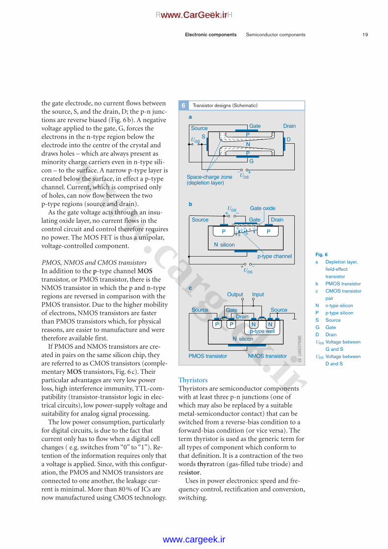
the gate electrode, no current flows betweenthe source, S, and the drain, D; the p-n junc-tions are reverse biased (Fig. 6 b). A negativevoltage applied to the gate, G, forces theelectrons in the n-type region below theelectrode into the centre of the crystal anddraws holes – which are always present asminority charge carriers even in n-type sili-con – to the surface. A narrow p-type layer iscreated below the surface, in effect a p-typechannel. Current, which is comprised onlyof holes, can now flow between the two p-type regions (source and drain).
As the gate voltage acts through an insu-lating oxide layer, no current flows in thecontrol circuit and control therefore requiresno power. The MOS FET is thus a unipolar,voltage-controlled component.
PMOS, NMOS and CMOS transistorsIn addition to the p-type channel MOStransistor, or PMOS transistor, there is theNMOS transistor in which the p and n-typeregions are reversed in comparison with thePMOS transistor. Due to the higher mobilityof electrons, NMOS transistors are fasterthan PMOS transistors which, for physicalreasons, are easier to manufacture and weretherefore available first.
If PMOS and NMOS transistors are cre-ated in pairs on the same silicon chip, theyare referred to as CMOS transistors (comple-mentary MOS transistors, Fig. 6c). Theirparticular advantages are very low powerloss, high interference immunity, TTL-com-patibility (transistor-transistor logic in elec-trical circuits), low power-supply voltage andsuitability for analog signal processing.
The low power consumption, particularlyfor digital circuits, is due to the fact thatcurrent only has to flow when a digital cellchanges ( e.g. switches from “0” to “1”). Re-tention of the information requires only thata voltage is applied. Since, with this configur-ation, the PMOS and NMOS transistors areconnected to one another, the leakage cur-rent is minimal. More than 80% of ICs arenow manufactured using CMOS technology.
ThyristorsThyristors are semiconductor componentswith at least three p-n junctions (one ofwhich may also be replaced by a suitablemetal-semiconductor contact) that can beswitched from a reverse-bias condition to aforward-bias condition (or vice versa). Theterm thyristor is used as the generic term forall types of component which conform tothat definition. It is a contraction of the twowords thyratron (gas-filled tube triode) andresistor.
Uses in power electronics: speed and fre-quency control, rectification and conversion,switching.
Electronic components Semiconductor components 19
Fig. 6a Depletion layer,
field-effecttransistor
b PMOS transistorc CMOS transistor
pairN n-type siliconP p-type siliconS SourceG GateD DrainUGS Voltage between
G and SUDS Voltage between
D and S
D
G
_ +UDS
UDS
UGS
UGS
SN
P
P
Space-charge zone (depletion layer)
Source Gate Drain
a
b
c
N
PMOS transistor NMOS transistor
Source
Output Input
GateDrain
Source
P P
silicon
NNp-type well
_+
_+
N
p-type channel
Source Gate
Gate oxide
Drain
PP+
+
++
+
silicon
Transistor designs (Schematic)6
æU
AE
0768
E
Robert Bosch GmbH
www.cargeek.ir
www.CarGeek.ir
www.cargeek.ir

Monolithic integrated circuits (ICs)
Monolithic integrationThe planar process is a method of manufac-turing semiconductors which makes it pos-sible to produce all components of a circuit(resistors, capacitors, diodes, transistors)and the conductive connections betweenthem on a single silicon chip in a single pro-duction process. It involves the creation ofmultiple p and n-type layers in a multi-stagedoping process using a pre-doped single-crystal silicon disc or wafer.An integrated circuit IC (Integrated Circuit,see section entitled “Manufacture of Semi-conductor Components and Circuits”) doesnot contain any “separate” (discrete) com-ponents but rather switching elements orfunctional elements.
Degree of integrationThe degree of integration is defined as thenumber of functional elements, transistorsor gates on a single chip. The following cate-gories are defined based on the degree ofintegration (and chip surface area): SSI (small-scale integration): up to
around 1000 elements per chip, averagechip area 3 mm2 (varies considerablydepending on level of power loss)
MSI (medium-scale integration): up toaround 10,000 elements per chip, averagechip area 8 mm2
LSI (large-scale integration): up to100,000 elements per chip, average chiparea 20 mm2
VLSI (very-large-scale integration): morethan 100,000 elements per chip, averagechip area 30 mm2
The number of functional elements onVLSI chips is constantly increasing. Micro-processors can now have up to 10 milliontransistor functions per chip. Memory mod-ules (DRAM) can even contain several hun-dred million transistors. The number ofsuch functional elements is subject to anexponential increase over time. This fact was first recognised by Gordon Moore
20 Electronic components Semiconductor components
Fig. 7a Increase in number of
transistors per chip inmemories andprocessors (GordonMoore’s Law)
b Fall in cost of transis-tors
c Decreasing size ofstructural units of new processors
Year
Stru
ctur
e si
ze
2
4
6
8
10m
01980 1990 20001970
8008: 10 m
8080: 6 m
III III
mmm
= 0.8 = 0.35= 0.18
Pentium I
II
III
8088: 3 m
386DX: 1,5 m
486DX: 1 m
US
cen
ts p
er tr
ansi
stor
0.01
0.1
1
10
100C
0.001
8080
8008
8088
386DX
486DX
PentiumI II
III
Tran
sist
ors
per
chip
10 K
100 K
1 M
10 M
100 M
1 Ga
b
c
MemoriesProcessors
1 K
8080
8008
8088
256
256
64
64
16
16
4
1 K
4
1 M
1 G
386DX
486DX
Pentium IIIIII
Development of monolithic integration on a singlechip in the period from 1970 to 2000(logarithmic representation in a and b).
7
æU
AE
0759
E
Robert Bosch GmbH
www.cargeek.ir
www.CarGeek.ir
www.cargeek.ir

(co-founder of the company Intel) and is ex-pressed by “Gordon Moore’s Law” (Fig. 7a):Elements per chip = 2(year – 1956) · 2/3
This law states that the number of func-tions per chip will double every 18 months.Since the structural units in which the chipsare manufactured are becoming smaller atthe same time as the number of functionalelements is growing, the size of the ships al-ters very little and the costs per transistor aresimilarly dropping exponentially (Fig. 7b).Thus the structural units of new processorshave shrunk over a period of 28 years from10 µm in 1972 to 0.18 µm in the year 2000(Fig. 7c).
The degrees of integration LSI and VLSIdemand methods such as CAD (computer-aided design). VLSI circuits in particular canonly be created with the help of highly so-phisticated programs which can convert en-tire function blocks into corresponding cir-cuit subdivisions. Such program systems arecalled HDL (Hardware Description Lan-guage) or VHDL (Visual HDL).
IC classificationThere are various systems for classifying ICs,although there are invariably mixed cate-gories within each system. Classification by method of production:
Bipolar/Unipolar (MOS);mixed category: e. g. BiCMOS, BCD
Classification by function:Analog/Digital;mixed category: e. g. mixed-signal IC
Classification by application:Standard IC/ASICmixed category: e. g. ASSP
ASIC (application-specific IC): developedand produced specifically for a particularapplication and exclusively for a particularcustomerASSP (application-specific standard prod-uct): developed and produced specificallyfor a particular application for a particularcustomer but is also sold to others for thesame type of application.
Apart from a few exceptions, ICs are nowalways based on MOS or combined technolo-gies, and for that reason bipolar ICs are notdescribed in any further detail at this point.
Analog circuitsAnalog circuits are required wherever elec-tronic equipment has to communicate withthe outside world – which is always analog.This applies in particular to the areas of“preparation” and “processing” of input andoutput signals. Examples of analog-inputsignal generators are microphones (tele-phone) and sensors. Examples of analog-output signal receivers are speakers or actua-tors.Figure 8 illustrates the stages of develop-ment of an analog IC from conception toinstallation in an ECU.
Electronic components Semiconductor components 21
Fig. 81 Development and
simulation 2 Layout3 Production4 Testing, analysis and
release 5 Packing, final testing6 Installation in an ECU
MVcc
Vccs
On/off
2
1
3
4
6
5
Development of an analog IC from conception to installation
8
æU
AE
0762
E
Robert Bosch GmbH
www.cargeek.ir
www.CarGeek.ir
www.cargeek.ir

Basic structures: stabilised-voltage sources,stabilised-current sources, differential am-plifier stages, coupling circuits, potentialshifting circuits, output stagesApplication-based ICs: operational ampli-fiers, voltage regulators, comparators,timers, transducers, interface circuitsSpecialised ICs: voltage references, broad-band amplifiers, analog multipliers, functiongenerators, phase-locking circuits, analogfilters and switches
Digital circuitsDigital circuits (Fig. 9) are used whereverlarge volumes of data have to be processedwithin a short space of time. High-perfor-mance microcontrollers in particular canperform several hundred million computa-tional operations per second. They are thusable to utilise the input data to provide therequired, highly accurate response at theoutput of the particular device. Similarly,large volumes of data can be transmitted viaa cable link in coded form, e.g. several thou-sand telephone calls can be transmitted si-
multaneously via a fibre-optic cable withoutcross-talk.
Since inputs and outputs for communi-cation with the real world always have to be analog, analog-digital converters (ADCs)are used at the inputs of a digital circuit, anddigital-analog converters (DACs) at the out-puts.
Digital systems make use of a whole series of recurring basic circuits and variations ofthem. The range extends from simple gatesto memories, microprocessors and micro-controllers.
Digital modules can only be connected upto form a complete system if power supplyvoltages, logic signal levels, switching speedsand signal transmission times are compat-ible. This requirement is met within a familyof circuits. Since, apart from a few spe-cialised applications mainly in military sys-tems, CMOS logic circuits are the only typenow used, such compatibility is no longer aproblem.
22 Electronic components Semiconductor components
Digital circuit on a chip9
æU
AE
0013
Y
Robert Bosch GmbH
www.cargeek.ir
www.CarGeek.ir
www.cargeek.ir

Mixed-signal ICsICs in which both analog and digital circuitelements are combined are called mixed-sig-nal ICs. They are an essential requirementfor the combination of entire electronicsystems on a single piece of silicon (SoC:System-on-a-Chip).
With ever-increasing degrees of integra-tion, this type of circuit is becoming moreand more attractive and the number of ap-plications is continually increasing. It is nowconceivable, for example, to integrate theentire electronic circuitry for a mobilephone or a complete Internet-access systemon a single chip. Where only low levels ofelectrical power are required, such as in theexamples quoted, both the analog and thedigital sections are manufactured usingCMOS technology.
Mixed-signal ICs for applications involv-ing higher electrical power levels, such as arefrequently encountered in automotive sys-tems, are typically hybrids of various tech-nologies, such as BCD systems (where Bstands for bipolar, C for CMOS and D forDMOS).
Figure 10 shows how the functions, “sens-ing”, “analysing” and “acting” are integratedin a mixed-signal IC. In such circuits, thebipolar section is used for converting theanalog inputs. The CMOS section of the ICperforms the logical processing operationsusing digital technology. The DMOS sectionenables high analog output performance.
Elements of digital circuitsDigital circuits assign voltage signals one ofthe two signal levels “0” (low voltage level)or “1” (high voltage level) and process thosesignals digitally. As digital circuits make upthe greater part of all ICs and our day-to-day lives are no longer conceivable withoutthem, a few typical circuit elements aredescribed below.
Gates Gates are logical-operation circuits with twoor more inputs. The input signals are logicallylinked to one another so that their variouscombinations determine the output signalsaccording to a defined logic (e.g. AND gate).
Electronic components Semiconductor components 23
Power (DMOS)Digital logic (CMOS)Analog (bipolar)
Acting
Analysing
Sensing
Mixed-signal IC10
æU
AE
0763
E
Robert Bosch GmbH
www.cargeek.ir
www.CarGeek.ir
www.cargeek.ir

InvertersInverters are digital circuits that convert thedigital input signal “0” into the output signal“1” and vice versa.
BusThe bus links up the individual elements ofa digital circuit; this relates both to connec-tions within an integrated circuit and theinterconnection of separate digital ICs.
A bus can connect up a large number ofseparate modules with different functionsbut with electrically identical interfaces. Aserial bus (e. g. for connecting up serialEEPROMs) transmits the data along a singlelead. A parallel bus (e. g. address bus, databus, control bus) is a bundle of parallel lines.The number of separate items of informa-tion that can be simultaneously transmitted(equal to the number of bus lines) is, to-gether with the data transmission speed, ameasure of the performance capacity of thedata bus. The most common types of busare 8-bit, 16-bit and 32-bit.
The dimensioning of the data bus is deter-mined by the capacity of the CPU (centralprocessing unit). In order for a system toachieve its maximum performance capa-bility (i.e. maximum processing speed) theCPU and data bus should have the samecapacity, i.e. an 8-bit CPU should use an 8-bit bus, a 16-bit CPU a 16-bit bus, etc.
In addition, the bus should be able totransmit the data as quickly as the CPU canprocess it. This is often not the case withexternal busses (e. g. CPU clock speedfCC = 400 MHz and bus clock speedfCB = 133 MHz).
Only one bus node at a time can write datato the bus. According to the bus type, thisaddresses the data in such a way that it canonly be read by the addressee, or else itswitches all other bus nodes off before send-ing the information and then on again after-wards.
Clock-pulse generator (CPG)A clock-pulse generator ensures that all op-erations on the microcomputer are synchro-nised with a defined timing pattern. Theclock-pulse generator must be matched tothe required speed of computing operations.
Input/output (I/O) unitThe I/O unit handles data exchange with theoutside world. The input signals are scannedat the required frequency. The output signalsare transmitted at the speed required by, andin the optimum order for, the applicationconcerned or are held in temporary storageuntil called for.
MicrocomputersThe microcomputer consists of the follow-ing interacting components (Fig. 11): A microprocessor as the CPU (central pro-
cessing unit). For its part, the micropro-cessor consists of the control unit and thearithmetic and logic unit. The arithmeticand logic unit performs arithmetical andlogical operations, as the name suggests,while the control unit carries out the in-structions from the program memory.
Input and output units (I/O units) whichhandle the exchange of data with periph-eral devices. Peripheral devices include in-put and output devices and external datastorage media.
A program memory in which the operatingprogram (user program) is permanentlystored (ROM, PROM or EPROM).
Data memories for holding the data beingprocessed at any particular time. This datachanges continually (RAM).
The bus system which links up the individ-ual components of the microcomputer.
A clock-pulse generator (oscillator) whichensures that all operations on the micro-computer are synchronised with a definedtiming pattern.
Logic circuits which are modules with spe-cialised tasks such as program interrupts.They are integrated in individual I/O units.
24 Electronic components Semiconductor components
Robert Bosch GmbH
www.cargeek.ir
www.CarGeek.ir
www.cargeek.ir

Electronic components Semiconductor components 25
I/O Bus
cont
rolle
r
Com
mun
icat
ion
with
ext
erna
lch
ips
via
addr
ess/
data
bus
Mic
rop
roce
sso
rC
entra
l Pro
cess
ing
Uni
t (C
PU
)
Arit
hmet
ic a
nd L
ogic
Uni
t (
ALU
)4-
, 8-,
16-,
32-b
it
Vo
latil
e re
ad/w
rite
m
emo
ry (
RA
M)
for
varia
ble
data
Mem
ory
capa
city
64 b
ytes
… 3
2 kb
ytes
Rea
d-o
nly
mem
ory
(RO
M, E
PR
OM
,fla
sh E
PR
OM
)F
or p
rogr
ams
and
perm
anen
t dat
a re
cord
s
Mem
ory
capa
city
2 kb
ytes
… 5
12 k
byte
s
No
n-v
ola
tile
read
/w
rite
mem
ory
(EE
PR
OM
)
Mem
ory
capa
city
32 b
ytes
…1
kbyt
e
Bu
s
4-,
8-, 1
6-, 3
2-bi
t dat
a ci
rcui
t C
lock
-pu
lse
gen
erat
or
(osc
illat
or)
I/OIn
terr
upt
cont
rolle
r
Mon
itorin
gci
rcui
t(w
atch
dog
)
I/OE
vent
coun
ter
Cou
nter
8 …
64
bit
I/OS
igna
l acq
uisi
tion
and
outp
ut w
ithtim
e re
fere
nce
(Tim
er, t
ime
proc
essi
ng u
nit,
inpu
t cap
ture
, ou
tput
-com
pare
re
gist
er)
Res
olut
ion
50
ns
Tim
e ra
nge
50 n
s …
1s
I/OA
nalo
g/D
igita
l(A
/D)
conv
erte
r
Res
olut
ion
8 …
10 b
it4
… 3
2 ch
anne
ls
I/OD
igita
l in
puts
/ou
tput
s
8 …
32
chan
nels
I/O Ser
ial
inte
rface
(UA
RT
,S
PI,
CA
N)
Dat
a ra
te20
0 bi
t/s
…1
Mbi
t/s
Mic
roco
mpu
ter
…
……
……
……
Microcomputers11
æU
AE
0454
-1E
Robert Bosch GmbH
www.cargeek.ir
www.CarGeek.ir
www.cargeek.ir

The chief components of a microcomputerare generally separate modules connected toone another on a printed-circuit board. Forsimpler tasks such as are more and more fre-quently required for Internet access on wire-less communication devices, single-chipcomputers are becoming increasingly com-mon. They integrate the functions detailedabove on a single silicon chip (System-on-a-Chip). The relatively small amount of RAMthat can be accommodated on a chip at rea-sonable cost limits the performance capabil-ities of such highly integrated systems.
MicroprocessorA microprocessor is a central processingunit (CPU) in the form of an integratedcircuit on a chip. The concept of the micro-processor avoids individualisation despitethe high degree of integration, and enablesadaptation to the multiplicity of practicaldemands by reliance on programming. Amicroprocessor is not capable of function-ing on its own; it is always part of a micro-computer. At present, there are 16-bit, 32-bitand 64-bit microprocessors. Processors aresubdivided into two main categories: PCs use CISC (Complex Instruction-Set
Computer) processors. These are ex-tremely versatile and permit unrestrictedprogramming.
Workstations normally use RISC(Reduced Instruction-Set Computer)processors. These perform specific taskssuch as are frequently required on work-stations much faster, but are distinctlyslower for all other tasks.
MicrocontrollersThe microcontroller is a component that in-corporates the following elements on a chip: CPU, random-access memory (RAM), peripheral modules (input/output, inter-
rupt, timer, serial interfaces) and an optional read-only memory (ROM).
With these integrated components, the mi-crocontroller is capable of stand-alone oper-
ation. For that reason, it is also referred to asa single-chip microcomputer.
The microcontroller is used to controlself-regulating systems such as an engine-management system.
At present, there is a choice of 4-bit, 8-bit,16-bit or 32-bit microcontrollers for thevarious types of application. Depending onapplication, they may also have expansionmodules connected to them (e.g. additionalmemory for data and program code).
The program that is run by the CPU ispermanently fixed in the read-only memoryand is not changed for different appli-cations. This distinguishes the single-chipmicrocontroller from the PC.
TransputerA transputer is a special type of micro-processor that is particularly suited to theconstruction of parallel computer networks.In addition to the usual components of amicroprocessor, it has communication andprocess-handling hardware on a chip.
ProgrammingThe only command form capable of directinterpretation by a microprocessor is a bitpattern, i.e. the binary representation of anumber. Since, however, this form of in-struction is not easy to work with for a pro-grammer, and is therefore susceptible toerrors, easily memorable abbreviations(mnemonics) are used. These are automati-cally translated by an assembler programinto bit patterns (machine code) that can beunderstood by the microprocessor. Micro-computers for single-purpose applicationsare programmed in the assembler languagespecific to the processor.
For more complex systems and programs,“high-level programming languages” such asC are needed, as otherwise it would be im-possible to keep extensive programs man-ageable and free of errors. Such languagesrequire sophisticated translation programs(compilers) which convert the text of thehigh-level language into a form that can beprocessed by the processor.
26 Electronic components Semiconductor components
Robert Bosch GmbH
www.cargeek.ir
www.CarGeek.ir
www.cargeek.ir

Semiconductor memoriesApplicationsMemories are used to store large volumes of Digital signals representing data
(I/O data, statuses, intermediate resultsinvolving frequent and rapid reading andwriting),
Program code (usually permanentlystored), and
Constants (permanently stored)
Storage involves recording (writing), permanent retention (actual storage), and location and retrieval (reading) of infor-
mation.
Memories make use of physical effects thatmake two different statuses clearly distin-guishable and easy to generate and identify.The advantage of semiconductor memorieslies in their technological compatibility withthe modules used in other parts of a com-puter, and thereby in new opportunities forfunctional integration.
Classification of semiconductor memoriesDigital signals are stored by utilising thestatus alternatives conducting/not conduct-ing or charged/uncharged. The most impor-tant terms are explained below according totheir standardised definitions, where applic-able, or their most common usage (seeFig. 12 for overview).
Random-access memory (RAM)Random-access memory or RAM is a short-term memory that allows direct access toany storage location. Information can beread/written from/to the memory any num-ber of times. However, it must exist in bi-nary form, i.e. encoded as a series of “yes orno” statuses (logical “1” or logical “0”). Sucha “yes or no” unit of information is called abit (binary digit). Random-access memories,like read-only memories, are organised on abit or word basis depending on the particu-lar application. A “word” is a group of bitsthat can be processed as a single unit. Theword length is equal to the number of bitsprocessed as a single unit. On microcompu-ters, word lengths of 4, 8, 16, 32 and 64 bitsare common. 8 bits make up one byte, i.e.1 byte = 8 bits.
Electronic components Semiconductor components 27
Programmable on a program-ming device
Programmablein the circuit
Semiconductor memories
Non-volatile memories Volatile memories
Factory programmed User programmed
Staticmemories
Dynamicmemories
Read-only UVerasable
ROMRead-only
memory
PROMProgram-
mable read-only memory
EPROMErasablePROM
FlashEEPROM
EEPROMElectricallyerasablePROM
SRAMStaticRAM
DRAMDynamic
RAM
Electrically erasable
Classification of semiconductor memories12
æU
AE
0465
-1E
Robert Bosch GmbH
www.cargeek.ir
www.CarGeek.ir
www.cargeek.ir

Memories can be organised on the basis of avariety of word lengths. The way the mem-ory is organised is generally indicated by amultiplication sign, e.g. an 8 M 8 RAM or8-megabyte RAM ≈ 8 million bytes = 64 million bits = 64 Mbit
That means that the memory has eight datainputs and eight data outputs at which theeight bits of one of the eight million storeddata words are simultaneously present. Itsword length is thus 8 bits. Since all memoryspecifications are based on the binary sys-tem, the exact number of bits is as follows:64 Mbit = 8 Mbyte 8 bit = 223 8 bit = 226 bit = 67,108,864 bits
Static RAM (SRAM)Static RAMs use bistable switching elementsas the data storage cells. Their function issimilar to that of a flip-flop, a simple circuit
with two transistors, of which either the one(logical “1”) or the other (logical “0”) con-ducts at any one time. In SRAM, the infor-mation remains stored until the storage cellconcerned is addressed and overwritten, orthe power supply is switched off.
Static RAMs are currently available insizes up to 16 Mbit. Although considerablymore expensive than dynamic RAMs, be-cause they can be written into and read sig-nificantly faster they are used as high-speedaccess computing memories (cache mem-ory) for the CPUs in computers. Typicalread-write times are currently less than30 ns.
Dynamic RAM (DRAM)The information in a DRAM is stored as anelectrical charge in the gate capacitor of aCMOS transistor which either passes (logi-cal “1”) or does not pass (logical “0”) a cur-rent as a result. As such capacitors are sus-ceptible to leakage, the charge is graduallylost. In order that the information (charge)is retained, the memory has to be refreshedat regular intervals (every few ms).
28 Electronic components Semiconductor components
5,00075,000
400
120
305 0.5 0.13 0.06 0.03
1973 1977 1981 1984 1987 1990 1995 1998 2001 2005
Car TVHouse Shirt PizzaBicycle1 Local phone
call
1 Stick ofchewing
gum
1 Paper clipStamp
CHEWING GUM
Growth in productivity of dynamic RAM (DRAM) in hindsight. Cost of 1 Mbit of memory capacity in Euro (€)
13
æU
AE
0773
E
Robert Bosch GmbH
www.cargeek.ir
www.CarGeek.ir
www.cargeek.ir

DRAMs are currently available commer-cially in sizes up to 256 Mbit (on one chip),and in laboratory conditions up to 1 Gbit(gigabit = 109 bit). Since every storage cellconsists of a transistor and a capacitor, thisrequires more than a billion transistors on asingle chip.
DRAMs are volatile memories. Thismeans that they lose their information whenpower is switched off.
DRAMs are very widely used nowadays assystem memories for all types of computer.The fall in price for 1 Mbit of memory overthe last few decades has been so dramaticthat ample memory can now be fitted in anyPC without substantially affecting its price(Fig. 13).
Read-only memory Read-only memory (ROM) is permanent-storage memory that allows any memorylocation to be accessed directly but – as thename indicates – allows the informationonly to be read and not altered.
A ROM is a non-volatile memory, i.e. theinformation it contains is retained evenwhen the power supply is switched off. It isusually used to store program codes (controlprograms) and fixed data (function tables,encoding rules, character generators, enginecharacteristic-data maps) that need to be re-trievable at any time. The information maybe indelibly entered in the memory either bythe manufacturer (in one of the last stages of production) or by the user by appropriateprogramming of specially prepared memo-ries (PROMs or programmable ROMs).
Erasable ROM There are also ROMs whose contents can beerased and reprogrammed as outlinedbelow.
EPROM (Erasable PROM)This type of erasable read-only memory canhave its contents completely wiped by irra-diation with UV light and can then be re-programmed. Such reprogramming is only
possible with special equipment at relativelyhigh cost.
EEPROM (Electrical EPROM) EEPROM is also referred to as E2PROM (Esquared PROM). This type of erasable read-only memory can be electrically wiped andreprogrammed. The wiping and reprogram-ming operation can be performed either in aseparate unit or in situ. Every storage cell ofan EEPROM be individually overwritten.For that reason, this type of memory mod-ule can also be used as non-volatile datamemory (e.g. for status information inengine-management systems).
Flash EEPROMYet another variation of EPROM andEEPROM is the flash EEPROM. In this case,electrical flash pulses are used to erase spe-cific storage areas or the entire contents ofthe memory. The erased areas can subse-quently be reprogrammed.
The flash memory can be reprogrammedon a programming station. However, the ad-vantage of flash EEPROM is that is can alsobe reprogrammed while still inside thesealed control unit. When this is done, thememory area which contains the program-ming routines must not be erased, or alter-natively, the programming routines must betransferred to the RAM before the memoryis wiped. The microcontroller then workswith the RAM as the program memory.Flash EEPROM is used wherever relativelylarge volumes of data need to be stored butalso have to be changed from time to time(e.g. in mobile phones, digital cameras andas program memories in electronic controlunits in motor vehicles).
Electronic components Semiconductor components 29
Robert Bosch GmbH
www.cargeek.ir
www.CarGeek.ir
www.cargeek.ir

Opto-electronic componentsPhotoresistorA photoresistor is a resistor whose resistancedecreases when exposed to light (Fig. 14).Light (photons) generates free charge carri-ers in the semiconductor as soon as the en-ergy of a photon is equal to the energy hold-ing a charge carrier within the lattice (inter-nal photoelectric effect).
Photoresistors generally consist of polycrys-talline semiconductor materials in which theeffect is particularly marked such as CdS,CdSe, PbS, PbSe, CdTe, ZnO, Se, InSb, InAs,Ge or Si.
A photoresistor is not equally sensitive toall wavelengths. Its maximum sensitivity lieswithin a narrow wavelength band that isspecific to the material used.
Photoresistors are mainly suitable for usein cameras as light meters.
PhotodiodeA photodiode is a semiconductor diodewhich utilises the depletion-layer photoelec-tric effect. Reverse voltage is applied to thep-n junction. Incident light releases elec-trons from the crystal lattice. As a result,additional free electrons and holes are pro-duced. They increase the reverse current(photoelectric current) in proportion to theintensity of the light (Fig. 15).
Photodiodes can be used in light meters,photoelectric beams and in positioning andremote control applications that use infraredlight.
Photovoltaic cellLike the photodiode, the photovoltaic cellreleases charge carriers when exposed tolight; no external voltage is applied to the p-n junction, however. If the electrons andholes reach the p-n junction, they are sepa-rated by the internal field of the space-charge region. A photoelectric voltage isgenerated which produces a photoelectriccurrent in the external circuit. Light energyis thus converted into electrical energy.
Photovoltaic cells are used to measurelight intensity and to generate electricitywith solar panels.
Light-emitting diodeThe light-emitting diode or LED emits lightwhen a forward current is passed through it.In other words, it operates in the oppositeway to the photodiode effect – free electronsand holes are recombined. The energy re-leased is emitted in the form of light.The semiconductor materials most com-monly used are gallium compounds such asgallium arsenide (GaAs) and gallium phos-phide (GaPh). The wavelength of the lightemitted by an LED depends on the semicon-ductor material used. There is now a choice
30 Electronic components Semiconductor components
Light intensity E
Res
ista
nce
R
600 800 1,000 lx
2
4
6
8
10
12
kΩ
400200
Photoresistor (characteristic)14
æU
AE
0917
E
Reverse voltage U
Pho
toel
ectri
c cu
rren
t I
V
0.1
0
0.2
0.3
0.4
0.5mA
0-0.1-0.2 20 40 60
1,000 lx
500 lx
2,000 lx
3,000 lx
4,000 lx
5,000 lxLight intensity E
80
Photodiode (characteristics)15
æU
AE
0761
E
Robert Bosch GmbH
www.cargeek.ir
www.CarGeek.ir
www.cargeek.ir

of colours available (infrared, red, yellow,green, blue).
LEDs are used for numerical and alphabeti-cal displays as well as for warning lamps.Since it has been possible more recently tosubstantially increase the amount of lightgenerated, LEDs are now also used in motorvehicles to illuminate the instrument panelor as a third (high-level) brake light. Theyhave the advantage of a relatively high lightyield and, as a result of their very long ser-vice life, do not have to be replaced.
Laser diodeWith the appropriate mechanical/opticaldesign, LEDs can also be made to emit laserlight, i.e. a parallel beam of monochromatic(of a single wavelength) and coherent (thewaves are in phase) light. Such properties arerequired for the transmission of data byfiber-optic cables. Laser diodes were there-fore a necessary requirement for the highdata flow rates such as occur in computernetworks with access to the Internet or thetransmission of television signals by cable.
PhototransistorA similar effect to that used by the photo-diode also occurs in the phototransistor. In-cident light striking the base alters the con-ductivity between the emitter and the collec-tor in such a way that a current proportionalto the intensity of the light is able to flowthrough the transistor. This type of compo-nent can thus be used as a switch for photo-electric beams, for instance.
There are also phototransistors that canbe operated the opposite way around so thatthey emit light. The advantage compared tothe LED is that the phototransistor can beswitched on and off very quickly. It is there-fore particularly suited for use in the manu-facture of flat screens. There is a transistorfor every screen dot (determined by thescreen raster in a cathode ray tube). As theareas required are generally substantiallylarger than the silicon slices available, andsuch slices would, in any case, be much too
expensive, flat screens are manufactured us-ing thin-film techniques (vapour depositionthrough a screen). The advantages of flatscreens over cathode-ray tubes are theirslimmer dimensions, lower power consump-tion and the absence of flicker.
Charge-coupled device (CCD)CCDs are integrated circuits arranged as acharge-coupled array. They are used torecord images in video and digital camerasas well as in scanners. Thousands or evenmillions of individual elements laid out in amatrix pattern (array) are created on a chip(Fig. 16). Digital cameras can record up to3.5 million pixels with a colour resolution of16 million colours. CCDs are not only capa-ble of converting the visual information intoelectrical signals, they can also store the datauntil it can be transferred to an externalstorage medium. To do this, the outputregister (5) is scanned at a high rate.
Electronic components Semiconductor components 31
Fig. 161 Column clock
pulse A1/A2
2 Photosensors 3 CCD array4 Row clock pulse
B1/B2
5 Output register6 Video output
B1
B2
4
A1
A2
1
2
3
65
CCD, image-sensor structure16
æU
AE
0717
-2Y
Robert Bosch GmbH
www.cargeek.ir
www.CarGeek.ir
www.cargeek.ir

Micromechanical sensorsIt has been possible for a number of yearsnow to manufacture some sensor compo-nents using silicon technology. Since a largenumber of sensors can be produced simul-taneously on a single silicon wafer in similarfashion to electronic components, the unitcosts are substantially lower than in the pro-duction of conventional sensors. In addi-tion, there is also the possibility of havingthe sensor signals electronically processeddirectly on the same chip.
Examples of micromechanical sensors: Magnetic-field sensors measure an exter-
nal magnetic field by purely electricalmeans.
Acceleration and pressure sensorsmeasure the relevant variables by thephysical deformation of specific areas of the silicon.
Temperature sensors utilise the change inconductivity of the semiconductor ma-terial according to temperature.
Chemical sensors make use of the effectwhereby certain chemicals (gases, liquids)alter the electrical conductivity of somesemiconductor materials in a very specificway.
Some of the more important examples ofsensors and their design are describedbelow.
Hall-effect sensor for detecting magneticfieldsAn electrical potential UH is generated at theedges of a thin plate through which a cur-rent is flowing if a magnetic field is actingperpendicular to the current flow IV
(Fig. 17). It is described by the formula
UH = RH · IS · B/dwhereUH Hall-effect voltage RH Hall-effect constantIV Supply current B Flux density of the magnetic field d Thickness of the plate
In metals, the Hall-effect constant is verysmall: RH ≈ 10–9 m3/As. In semiconductors,RH is five orders of magnitude greater, e.g. Indium antimonide (InSb)
RH ≈ 2.4 · 10–4 m3/As, Indium arsenide (InAs)
RH ≈ 1.2 · 10–4 m3/As.
Hall-effect sensors can be used in motorvehicles as position sensors (e.g. for sensingcamshaft position). The advantage of thismeasurement principle is that position canbe detected even when the component con-cerned is not moving. By comparison, in-ductive speed sensors only produce anelectrical signal above a certain minimumrotational speed.
32 Electronic components Semiconductor components
Fig. 17A1, A2 Measurement
points for the Hall-effect voltage
B Flux density of themagnetic field
IV Supply currentIH Hall-effect currentUH Hall-effect voltaged Thickness of the
plate
S
N
d A1
A2
IH
IV
B
UH
Hall effect17
æU
AE
0023
Y
Robert Bosch GmbH
www.cargeek.ir
www.CarGeek.ir
www.cargeek.ir

Pressure sensorFigure 18 shows the structure of a microme-chanical pressure sensor. The silicon chip (2)is attached to a glass base (4) through whichthere is a hole which acts as the pressurechannel for the pressure p that is to bemeasured. At the point where the measuredpressure acts on the silicon chip, it has beenhollowed out on the underside. Conse-quently, the chip is in effect a thin dia-phragm (1) at that point, and deformsunder the action of pressure.
Attached to the top of the diaphragmthere are resistors which change their resis-tance in response to physical deformation(piezoresistive effect). By measuring the re-sistance, the pressure can be calculated withthe aid of the integrated bridge circuit.
Pressure sensors are used in motor vehiclesfor such tasks as measuring the intake mani-fold pressure and the atmospheric pressure.
Acceleration sensorFinger-like structures are etched into thesurface of a silicon ship (Fig. 19). Everyother “finger” is rigidly attached to the chip,while the alternate fingers are only attachedat one end so that they can oscillate freely atthe other. These fingers are connected up asa multi-layer capacitor. If the sensor is accel-erated in a particular direction, the distancebetween the fixed and the movable fingerschanges, thus altering the capacitance. Thatchange can be measured as an electrical sig-nal from which the acceleration can then becalculated.
Acceleration sensors are used in motorvehicles wherever changes in the vehicle’sdynamic behaviour need to be detected.
They are employed, for example, to triggerthe airbags in the event of an accident(abrupt deceleration).
The Electronic Stability Program (ESP)uses a yaw rate sensor to detect the rate ofrotation of the vehicle around its own axisand counteracts such yawing motion at anearly stage by controlled operation of thebrakes.
Electronic components Semiconductor components 33
Fig. 181 Diaphragm2 Silicon chip3 Reference vacuum4 Glass base (Pyrex)5 Bridge circuitU0 Supply voltageUM Measurement
voltageStrain resistors R1
(compressed) and R2
(stretched)
p
1 3
2
5
R1 R1R2
4
UM U0
R1
R2
R2
R1
Pressure-sensor cell with reference vacuum on the structural side
18
æU
AE
0017
-1Y
Detail of finger structure of a micromechanical silicon acceleration sensor
19
æU
AE
0817
Y
Robert Bosch GmbH
www.cargeek.ir
www.CarGeek.ir
www.cargeek.ir

Microcontrollers are single-chip computersthat are used for event-driven control sys-tems or for controlling technical processes.Modern-day life is no longer conceivablewithout them and they are to be foundwherever control systems for electricallyoperated devices are required.
MicrocontrollerdevelopmentsFive billion microcontrollers were producedin 1999, that is roughly equivalent to one forevery person on the Earth. Its triumphantmarch into every aspect of our day-to-daylives is clearly demonstrated by the numberof microcontrollers produced in the last tenyears (Fig. 1).
A microcontroller consists of the inte-gration of a CPU (central processing unit)with memories and peripheral circuits on asingle chip. These are referred to as “embed-ded systems”. Frequently such systems incor-porate a microprocessor that was originallydeveloped for computer applications andsubsequently adapted and modified so as tobe marketed as part of an embedded system.
Nevertheless, there are also many micro-controller architectures that were developedfrom the outset as controllers. They includethe M-Core™, the TriCore™ and theSH7000, 8051 and C166 families. Such mi-crocontrollers are characterised by rapiddata exchange with their environment, lowpower consumption, high data density andlow production costs.
What then is the actual origin of microcon-trollers? Even before the transistor was in-vented, most of the devices in which micro-controllers are now used were already in ex-istence – cars, telephones, radios, televisionsand household appliances. The differencewas that for most applications the controlsystems were mechanical and only in veryrare and very costly exceptions were func-tions controlled by electron tubes and relays.In addition to their high cost, the problem
of such control systems was that their relia-bility was heavily influenced by manufactur-ing tolerances, environmental conditionsand wear.
In the 1960s, Intel, followed shortly after-wards by Motorola, developed the firstmicroprocessors – initially for use in cashregisters. Following the development of inte-grated circuits and the first microprocessors,the inexorable progress of digital technologybegan in earnest in the 1970s. For the firsttime, it was now possible to eliminate a largenumber of interference factors.
The end of the 1970s saw the dawn of theage of the single-chip microcomputer.Prominent representatives of that periodwere the Intel 8048 and Motorola 6800 mi-crocontrollers, the structure of which is stillthe basis for many of today’s microcon-trollers. In the succeeding period, advancesin high-integration technology allowedmore and more peripheral circuits to be in-corporated in the chip. These were the be-
34 Microcontrollers Microcontroller development
Microcontrollers
01990 1992 1994
Year
1996 1998 2000
1
2
3
4
5
6
7
Uni
ts in
bill
ions
per
yea
r
Unit production figures for microcontrollers1
æS
AE
0879
E
Robert Bosch GmbH
www.cargeek.ir
www.CarGeek.ir
www.cargeek.ir

ginnings of the microcontroller as we knowit today.
In parallel with these developments, scien-tists realised that single-chip computerscould be used to perform control tasks inmotor vehicles. The first applications involv-ing high data volumes were the managementsystems for internal-combustion engines,followed later on by antilock braking sys-tems (ABS) and entertainment systems.
At the end of the 1980s, the term “embeddedcontrol system” was introduced to distin-guish them from infinitely programmablesystems such as the PC. Embedded systemsare designed exclusively for a specific appli-cation so that the entire program togetherwith the vehicle-specific data in a ROM orEPROM are a permanent part of the prod-uct that cannot be altered by the user.
Most microcontrollers sold today have an 8-bit CPU. Although the numbers of morepowerful 16 and 32-bit controllers are con-
tinually growing, simple 4-bit designs arestill used in large quantities (Fig. 2).
Microcontrollers are produced in a varietyof designs for a vast range of applications.The various types differ by virtue of thechoice of integrated memory and the pe-ripheral modules offered. The range ofintegrated memories available encompassesRAM, ROM, EEPROM and, more recently,flash EPROM.
To make it worthwhile to develop a stand-alone microcontroller design, the produc-tion figures should run to at least 1 millionunits a year. The unit price will then bebetween 0.5 and 15 Euro.
Applications that hold the promise ofsuch production volumes include controlsystems for automotive applications, com-munications devices, computer peripherals,domestic appliances and entertainment sys-tems. In addition, microcontrollers are alsopopular in industrial electronics, automa-tion systems and testing and measuringequipment, although recourse is generallymade to standard products.
Microcontrollers Microcontroller development 35
70%
60%
50%
40%
30%
20%
10%
0%
Microcontrollers
4 Bit 8 Bit 16 Bit 32 Bit
Proportion of microcontroller production volume by processor type (1999 figures)
2
æS
AE
0880
E
Robert Bosch GmbH
www.cargeek.ir
www.CarGeek.ir
www.cargeek.ir

Microcontroller componentsThe microcontroller is a programmableelectronic module that contains all the nec-essary components for a microcomputersystem. It consists of the CPU, the memories for instructions (program
memory) and data (data memory), and the peripheral modules.
Those components exchange data and mon-itoring information via bus links (Fig. 1).
CPUThe CPU (central processing unit; also re-ferred to as the microcontroller core) is theprogrammable unit for addressing and ma-nipulating data and for controlling the tim-ing and logical sequence of a program.
MemoryThe memory is used to store data and pro-gram instructions. The memory for variabledata is a random-access memory (RAM).The memory used for program instructionsand unvarying data is a read-only memory(e.g. ROM or PROM). In addition, micro-controllers have a small register memory in-tegrated in the CPU for rapid access (cachememory).
PeripheralsThe peripherals are used for the input andoutput of data originating from or destinedfor external systems. The peripherals areprogrammable to a limited degree in orderthat their functions are adaptable to therequirements of the application.
Typical peripheral modules digitise analogexternal signals or convert internal digitalsignals into analog signals for output (ana-log-digital and digital-analog converters).Counters and timers count external pulsesand time intervals between events. Commu-nication interfaces are used for the exchange
36 Microcontrollers Microcontroller components
Datastorage
Datamanipulation
Data exchangeData event monitoring
Memory
Data and program memory
Bus
Microcontroller core(CPU)
Peripheral modules
Arithmetic logic unit (ALU)
Program monitoring unit
Bus
Bus
Bus
Bus
Input and output units, ADC/DAC, timer, serial interfaces
Interruptsystem
Structure of a microcontroller with the “Von-Neumann architecture”1
æS
AE
0881
E
Robert Bosch GmbH
www.cargeek.ir
www.CarGeek.ir
www.cargeek.ir

of data with other modules via standardisedbus links (e.g. CAN bus).
There are, of course, many other func-tions that can be integrated in the microcon-troller depending on the requirements of theuser concerned.
Main operationsThe three blocks illustrated in Figure 1enable the four main operations of themicrocontroller, i.e. data manipulation (data processing), data storage, data exchange with external systems
(data movement), and data event monitoring (control mecha-
nism).
These functions enable the microcontrollerto be used to transfer, store and manipulatedata (both in the memory and externally).The sections which follow describe the vari-ous modules of the microcontroller thatmake those operations possible.
Design and operatingconceptCPU (Central Processing Unit)The CPU processes the data received fromexternal sources via the peripherals andmonitors the data flow. In the CPU there is asmall memory (register) in which operands,results and addresses are stored. Figure 2shows the basic structure of a CPU, whichmay also be extended by additional compo-nents in order to increase the processingspeed.
Programming modelThe “programming model” of a microcon-troller refers to the sum total of all registersthat are available to, i.e. are “visible” to, theprogrammer. In principle, there does nothave to be any “visible” register in the CPU.But in that case, every alteration to the pro-gram would necessitate modification of thehardware, which would be very involved, ex-pensive and time-consuming. Rarely alteredconfigurations are therefore set by means ofbits in special control registers. The control
Microcontrollers Microcontroller components, design and operating concept 37
Data and program memory
Peripherals(I/O)Arithmetic
logic unit (ALU)
Data
Control signalsImmediate data element
Relative address
Addresses
Instruction address
Instruc-tions and data
Operandregister
Operandregister
Memory data buffer
Memory data buffer
Instruction pointer(program counter)
Instruction register
Control circuits
Data and address manipulationProgram control Memory
Basic structure of a CPU (microcontroller core)2
æS
AE
0882
E
Robert Bosch GmbH
www.cargeek.ir
www.CarGeek.ir
www.cargeek.ir

registers are thus quasi-static extensions tothe instructions. The interrupt control regis-ter, for example, specifies which interruptsare allowed and which are barred. Othercontrol registers define the function of theALU (arithmetic logic unit) or the periph-eral modules.
Various operations can alter the operatingstatus of the microcontroller. If, for example,a signal is received from an external source(interrupt), this generally causes the pro-gram sequence to divert to a defined mem-ory address. While the interrupt service rou-tine at that location is being processed, onlysignals with a higher priority can interruptthat procedure. All other interrupt requestsare stored and only processed once the inter-rupt service routine in progress has beencompleted.
The status information that accrues in theprocess could be temporarily stored in theinstruction memory. However, this wouldresult in very long instructions. For that rea-son, special registers that store the status ofthe CPU are integrated in it in addition tothe control registers. These status registersinclude, among others, the program statusregister, the interrupt status register, themultiplier status word, etc.
In order to reduce the number of loadingand storage operations by the microcon-troller, the register file architecture incorpo-rates several accumulators (special computa-tion registers in the CPU). These enable in-terim results or important variables to beheld in the CPU. This increases the maxi-mum clock speed and reduces power con-sumption.
Operand memoriesDepending on the instruction-set architec-ture, there are various possible ways of pro-viding the operands (data to be linked) in-volved in mathematical calculations or logi-cal operations before and after the comput-ing operation.
Memory-memory architectureThe memory-memory architecture uses thegeneral random-access memory (RAM) toprovide the operands. When doing so, it en-codes the memory addresses of the operandsand the result of a mathematical operation(function that links the operands) explicitlyin the instruction. In that way, for example,two numbers that are both stored in thememory can be added together with a singleinstruction. The result can then be writtenback to the memory immediately. The term“memory-memory architecture” is derivedfrom the storage location of the operands.
Accumulator architectureWith the accumulator architecture, the CPUhas an integral memory cell that is perma-nently defined as both the source and thedestination of every mathematical opera-tion. This memory cell is called the accu-mulator. Only the address of the secondoperand is encoded in the instruction. Be-fore every mathematical operation, the firstoperand must be copied from the memoryto the accumulator by a load command. Fol-lowing the operation, the result is copiedback from the accumulator to the memory.
Memory-register architectureIn a memory-register architecture, there is awhole series of special memory cells calledregisters integrated in the CPU. Bothoperands are explicitly encoded in the in-struction. However, only one of the twooperands can be addressed directly in thememory using the memory address. Thesecond operand and the result are addressedin a register. As in the case of the accumula-tor architecture, one of the operands mustbe copied from the memory to a registerbefore the mathematical operation is per-formed. Following the operation, the resultmust then be written back to the memory.If, however, the number of registers is largeenough, interim results can be held in regis-ters rather than being continually copiedbackwards and forwards. The term “mem-
38 Microcontrollers Design and operating concept
Robert Bosch GmbH
www.cargeek.ir
www.CarGeek.ir
www.cargeek.ir

ory-register architecture” is derived from thelocation of the operands.
Register-register architectureThis last architecture category – also called“load-store architecture” – addresses bothoperands of an operation explicitly in theregisters. Before any mathematical opera-tion, therefore, both operands first have tobe loaded into a register. The result is thencopied back to the memory.
Operand addressesAnother important distinguishing featureamong instruction-set architectures is thepossible number of implicitly and explicitlyencoded addresses. The operation C = A + Brequires three addresses: the address of operand A, the address of operand B, and the address of the result operand C.
Instruction-set architectures which allowfree choice of these three addresses (possi-bility of encoding three addresses) are re-ferred to as “non-destructive instruction-setarchitectures”. But as three addresses nor-mally occupy too many bits in the instruc-tion code, many architectures use an implicitmethod of addressing.
With implicit addressing, one of the ad-dresses of the two source operands is alsoused as the destination address. Thus, theaddress of one of the source operands isused to store the result of the operation, andthat means that the operand in question isoverwritten, i.e. destroyed. That “destruc-tion” has led to the adoption of the term“destructive instruction-set architecture”.
Requirements placed on instructionsInstruction-set architectures differ from oneanother not only by virtue of their operandmemories and operand addresses, but alsoon the basis of the length of their instruc-tions. The following two very different re-quirements must be met in this connection:
Number of bits available for encodingDifferent operations require very widelyvarying numbers of bits for encoding in-structions of different levels of complexity.For example, the null operation NOP (NoOperation) requires no operators (no ad-dresses) nor any additional bits for definingthe precise function. The operation MAC(Multiply & Accumulate: A = A + (B C)),on the other hand, requires three operatorsand additional bits for encoding the func-tion, such as the behaviour in the event of amathematical overflow (saturation addi-tion), identifying the data format (Q for-mat), etc.
Decoding complexityInstructions of differing lengths are difficultto decode. First of all, the length of the cur-rent instruction has to be established. Thenthere is a check as to whether the instructionhas been completely read. Both operationsgenerally require several clock cycles andlimit the possible processing speed to a sub-stantial degree.
Length of instructionsThere are currently three different conceptsfor the length of instructions.
Fixed-length instruction set: every instruc-tion is the same length, e.g. always 16 bits.
Multiple instruction sets: it is possible toalternate between two different fixed-length instruction sets, e.g. 16 bits and32 bits. The first bit of each instructionthen indicates the format.
Multiple instruction length: the length ofthe instructions varies according to com-plexity, e.g. the NOP command can have alength of 16 bits and the intersegmentjump a length of 32 bits.
Instruction setThe complete instruction set of a microcon-troller enables it to execute any expression ofa higher-level programming language (e.g.C) by a sequence of instructions. The in-structions are classified as follows:
Microcontrollers Design and operating concept 39
Robert Bosch GmbH
www.cargeek.ir
www.CarGeek.ir
www.cargeek.ir

Data processing operations: mathematical,logical and conversion instructions.
Control instructions: jumps, comparisons,etc.
Input/output instructions: instructions forinputting and outputting data.
Memory instructions: instructions forreading and writing data from/to thememory.
The bits available in an instruction for ad-dressing the operands/result are limited.Embedded applications, however, requireever larger programs and data volumes,which leads to larger and larger numbers ofaddresses. As a result, the addresses becomelonger and longer and encoding them be-comes more and more complex. There are anumber of different methods for solving thisproblem.
Instruction executionExecution of instructions on modernmicrocontrollersThe various phases of instruction executionare illustrated in Figure 3. Fetch-instruction phase(1): before an in-
struction can be executed, it has to befetched from the program memory to the
CPU. This involves first calculating itsaddress, which is required in order to loadthe instruction into the CPU.
Decode-instruction phase (2): the instruc-tion transferred to the CPU is analysed.The relevant function is then initiated.
Fetch-operand phase (3): the operands arefetched from the registers or memories tothe executing unit (e.g. ALU).
Execute phase (data operations) (4): oncethe operands have been transferred to theexecuting unit, the data operation speci-fied by the instruction is executed.
Store-operand phase (5): the result of thedata operation is written back to a registeror memory in this phase (which is there-fore also called the “write-back phase”).
Execution of instructions on oldermicrocontrollersOn older microcontrollers, instructions areprocessed purely sequentially (CISC archi-tecture: Complex Instruction-Set Com-puter). This requires a complete clock cyclefor each phase: Phase 1: calculating the next instruction
address and reading the instruction Phase 2: decoding the instruction
40 Microcontrollers Design and operating concept
Fig. 3The numbers indicatethe five phases of execu-tion of an instruction
Requestinstruction
Vectoroperation
Nextinstruction
Requestoperand
Multiple operands
Indirect operand addressing
Indirect result addressing
Multipleresults
Decodeinstruction
2Calculateaddress
Dataoperation
4Calculateaddress
Fetchinstruction
1
Fetchoperand
3
Storeoperand
5
Calculateaddress
The phases of instruction execution on modern microcontrollers3
æS
AE
0883
E
Robert Bosch GmbH
www.cargeek.ir
www.CarGeek.ir
www.cargeek.ir

Phase 3: calculating the operand addressand reading the operand
Phase 4: executing the data operation Phase 5: calculating the address and
storing the result Phase 6: additional cycles for calculating
indirect addresses.
Sequential execution is necessary with thisprocess because certain units of the CPU areused a number of times in different phases.The arithmetic logic unit (ALU) in particu-lar is used to calculate all addresses (instruc-tion, operand, result, indirect address) andto execute the data operation. That meansthat the ALU is in use in every phase.
Parallel execution of instructionsBy adding extra address calculation units(address ALUs), the various operations canbe performed simultaneously. Thus, whileone instruction is being decoded, the next isbeing addressed and loaded (pipelining).This is the way in which RISC (Reduced In-struction Set Computer) architectures gen-erally operate. A RISC architecture is distin-guished by the following characteristics: reduced number of instructions, large number of general-purpose regis-
ters, and optimised pipeline.
In a microcontroller with a pipeline archi-tecture, the execution of multiple consecu-tive instructions is handled simultaneously.Rather like on a conveyor belt, the variousinstructions are at differing stages of execu-tion and it is not possible to reduce theexecution time of individual instructions.
In order to ensure that one instruction iscompleted in each cycle, all stages of apipeline must operate simultaneously andindependently of one another. Once theCPU pipeline is full, one instruction is com-pleted in each clock cycle.
Microcontroller memoriesIt is the job of memories to store both data(constants and variables) and the instruc-tions of a program and to make them avail-able when required.
There are a number of different ways inwhich memories are implemented. Thisrange of alternatives is necessary becausethere is no single implementation whichsuits all requirements. In order to satisfy thedifferent requirements, microcontrollersusually have several different memoryblocks.
The features by which memories aredistinguished include the implementationlocation, the method of addressing data, theaccess method and volatility/non-volatility.
Implementation location External to the microcontroller (external
memory), Integrated as separate module on the
microcontroller (internal memory) or Integrated as a submodule in a peripheral
module on the microcontroller (e.g.timer) or in the CPU (register)
Data addressing Free access (reading or writing) to all data
by allocation of a fixed address (RAM:random-access memory).
Direct addressing: specification of thememory address by an external source(e.g. the programmer)
Indirect addressing: the microcontrollercalculates the address itself according toexternal events
Content-related access to data by address-ing based on the data content. For exam-ple, address the word whose first bit is“one” (CAM: content addressable mem-ory, or associative memory). This type ofmemory is used in CAN communicationmodules, for example.
Microcontrollers Design and operating concept, microcontroller memories 41
Robert Bosch GmbH
www.cargeek.ir
www.CarGeek.ir
www.cargeek.ir
Sequential access to data with the aid of ahard-wired buffer structure (e.g. FIFO:first in, first out; LIFO: last in, first out).These memories are primarily used forsynchronising separate processor elements(e.g. microcontroller for antilock brakingsystem [ABS] with two CPUs).
Access Read-only memory (ROM), Random-access memory (RAM), or Erasable read-only memory (EPROM).
Volatility/Non-volatility Volatile: data is lost when the power
supply is switched off, or Non-volatile: data is retained when the
power supply is switched off
A RAM that has a back-up power supplyfrom a battery can act as a non-volatilememory.
Microcontroller peripheralmodulesIn addition to the CPU and the memory, theperipheral modules (input/output modulesor I/O modules) are essential components ofmicrocontrollers. They make it possible toacquire external signals in a variety of waysand to manipulate the controlled variablesby means of outgoing signals. Peripheralmodules represent an “intelligent” link be-tween the microcontroller and its environ-ment. Each module has an internal connec-tion to a system bus and external connec-tions to sensors and actuators.
Figure 4 shows a schematic diagram of thestructure of a peripheral module. Its taskscan be subdivided into the following: Communication with the internal system
bus, Communication with the environment, Data storage, Monitoring and timing, and Fault detection.
Peripheral modules: AddressingIsolated peripherals (isolated I/O)There are two separate address areas formemory and peripherals. Programming ofthe peripherals is strictly limited in this caseas only special instructions can be used forperipheral modules.
Memory-mapped peripherals (memory-mapped I/O)Peripherals and memory modules share acommon address area. The advantage of thisis that the large number of instructions foraddressing memories can also be used forperipheral modules. However, this uses upvaluable address space which can be disad-vantageous with 4-bit and 8-bit microcon-trollers.
Microcontrollers with 16-bit or 32-bit datawidth now almost exclusively use memory-mapped peripheral architectures.
42 Microcontrollers Microcontroller memories, microcontroller peripheral modules
Robert Bosch GmbH
www.cargeek.ir
www.CarGeek.ir
www.cargeek.ir

Peripheral modules: Operating modeAnother characteristic for distinguishing be-tween I/O modules is the mode of opera-tion, which can be one of the following:
Programmed I/OThe I/O module is controlled directly by theCPU. The microcontroller controls all func-tions by means of a program. In this case,the CPU has to wait while the I/O unit per-forms an operation. This mode of operationis therefore only used with microcontrollersthat exclusively perform input and outputoperations (I/O processors).
Polled I/OThe I/O module is capable of performingindependent operations and the input/out-put data is temporarily stored in specialbuffer memories. The CPU periodicallychecks the module status and transfers newdata as required. This mode of operation isprimarily suited to RISC microcontrollers asthey only have a software interrupt system.
Although the periodic scanning of theI/O module demands a large proportion of the CPU resources, polled I/O is ideallysuited to time-based operating systems(time-triggered architecture or TTA),e.g. OSEK+ (Offene Systeme und derenSchnittstellen für die Elektronik im Kraft-
fahrzeug [Open Systems and their Interfacesfor Electronics in Motor Vehicles]).
Interrupt-driven I/OThe peripheral module processes all inputand output operations independently andsignals to the CPU via a dedicated line(interrupt line) when new information isreceived or when an action by the CPU isrequired. The basic advantage of this is thatthe CPU and the peripheral modules canwork in parallel. The CPU program only hasto be interrupted when the peripherals needassistance. Checking of the programs for er-rors, however, is extremely time-consumingbecause all interrupt constellations have tobe checked. This architecture supportsevent-driven operating systems such asWindows CE, OSEK or OS9.
DMA (Direct Memory Access) I/OWith this mode of operation, the I/O mod-ules can exchange data directly with thememory, without the involvement of theCPU. This mode is primarily used for “high-end” microcontroller systems. As with inter-rupt-driven I/O, this mode of operation re-quires hardware that prioritises all pendingrequests.
Microcontrollers Microcontroller peripheral modules 43
Control logic
Status register
Address bus
Data bus
Control leads
Control register(monitoring,
error detection)
Sensors
Externalinterfaces
Data register
Com
mun
icat
ion
with
envi
ronm
ent
Com
mun
icat
ion
with
in
tern
al s
yste
m b
usD
ata
stor
age
Schematic diagram of a peripheral module4
æS
AE
0884
E
Robert Bosch GmbH
www.cargeek.ir
www.CarGeek.ir
www.cargeek.ir

Microcontroller bussesThe electrical connections between themodules of a microcontroller (e.g. CPU, pe-ripherals, memory, I/O modules, externalbus modules) are referred to as busses.
DesignBusses generally consist of two groups ofconnections: a data bus for transferring data, an address bus for transferring the ad-
dresses of data, and a control line for controlling communica-
tion between the sender and receiver ofthe data.
44 Microcontrollers Microcontroller busses
Harvard architectureVon-Neumann architecture
Extended Harvard architecture(dual-ported data memory)
Extended Harvard architecture(two data memories)
c d
a b
Microcontrollercore
Data memory1
Instructionmemory
Peripherals Externalbus controller
Data memory2
Microcontrollercore
Instructionmemory
Dual-porteddata memory
Peripherals Externalbus controller
Data memory Microcontrollercore
Instructionmemory
Peripherals Peripherals Externalbus controller
Data memory Microcontrollercore
Instructionmemory
Peripherals Peripherals Externalbus controller
Common bus architectures for embedded microcontrollers5
æS
AE
0885
E
Robert Bosch GmbH
www.cargeek.ir
www.CarGeek.ir
www.cargeek.ir

Operating conceptThe transfer of data involves the followingsequence of operations: The data is specified by a signal placed on
the address bus. Signals on control lines indicate the valid-
ity of the address. The address is read by the receiver/sender
of the data element (data source). The sender places the data element on the
data bus. The sender of the data element signals the
validity of the data element. The receiver of the data element reads the
data.
In order to achieve faster cycle times, theseoperations can be performed simultaneouslyon some busses (interleaved or pipelinedbusses). With interleaved busses, only theunidirectional runtime (drain source orsource drain) has to be considered, ratherthan the bi-directional runtime (drain source drain).
Common bus architecturesVon-Neumann architectureIf a microcontroller has only one bus viawhich the instructions for the CPU are readand the data is exchanged, this arrangementis referred to as the “Von-Neumann archi-tecture” (Fig. 5a). This architecture is char-acterised by the small amount of space itrequires on the semiconductor chip.
The data memory, the program memoryand the I/O modules are arranged across alinear address range. Because the bus isshared, only one signal, one item of data orone instruction can be read from the mem-ory at a time. Instructions that read datafrom the memory therefore require at leasttwo cycles.
Harvard architectureWhere a microcontroller has two busses (for data communication and transfer ofinstructions), it is said to have a “Harvardarchitecture” (Fig. 5b).
The Harvard architecture uses separate ad-dress areas for data memory and peripheralson the one hand and program memory onthe other, with each area being accessed by aseparate bus. This means that an instructioncan be read at the same time as an item ofdata is read or written. For embedded appli-cations, however, it has become evident thatseparation reduces performance. MostHarvard architectures therefore incorporatebridges which allow transfer of data betweenthe busses.
Digital signal processing generally involvesoperations performed on two operands (e.g.filter coefficient, item of data). In order notto have to read these two operands one afterthe other via the same bus, multiple data busarrangements referred to as extendedHarvard architectures were introduced. Withsuch arrangements, two items of data can beread simultaneously.
Extended Harvard architectures may alsohave two different data memories connectedto the two data busses (Fig. 5c) or one datamemory with two simultaneous access paths(dual-ported data memory) as illustrated inFigure 5d.
Microcontrollers Microcontroller busses 45
Robert Bosch GmbH
www.cargeek.ir
www.CarGeek.ir
www.cargeek.ir

The interaction between a circuit and mi-crocontrollers (µC) is best explained bymeans of an example. The circuit used inthe example chosen is referred to as a devel-opment circuit because it is used to test userprograms developed on a PC. Such circuitsare sometimes also called evaluationboards.
Overview
A development circuit is part of a develop-ment system used in conjunction with a PC.Figure 1 shows the overall layout of a devel-opment workstation with the circuit de-scribed in this example.The advantage of a development circuit isthat all components are easily accessible. Inaddition, the signals of the various inputsand outputs can be tapped at the terminals.In that way individual signals can easily bechecked.
Development environmentProgram development The user program is created on a PC using atext editor (source code, Fig. 2a). A compilerthen translates the source code from theprogramming language in which it is written(e.g. C++) into an assembly language basedon mnemonics. The assembly language isthe preliminary stage to the machine lan-guage and is still easy to read. An assembleris then used to convert the assembly lan-guage into a digital code that can be under-stood by the development circuit’s micro-controller. The precise memory addressesare specified by a linker. The machine codeor object code can then be transferred to the circuit by the PC.
Assembler programs can also generate list-ing files in which each line of the originalsource code is shown alongside the corre-sponding object code. This is useful forlocating errors.
46 Circuit example Overview
Circuit example
Fig. 11 Circuit signal on the
oscilloscope2 Output indicators
(LEDs)3 Development circuit4 Connection to PC
(connector X2)5 19-inch module rack
system with powersupply unit
6 Circuit layout7 Circuit diagram8 Example program
1
7
65
4
3
2
8
Components of a development workstation with the development circuit1æ
UA
E08
46Y
Robert Bosch GmbH
www.cargeek.ir
www.CarGeek.ir
www.cargeek.ir

Transferring the object codeThe object code is transferred (downloaded)by starting a program on the PC that trans-mits the file containing the object code viathe PC’s RS232 interface. This interface isconnected by a lead and the connector X2 to the circuit (Fig. 2b).
Monitoring program (basic program)A fixed monitoring program running on themicrocontroller reads the data sent by thePC and stores the object code in the devel-opment circuit’s RAM (external RAM).
The monitoring program is stored in theROM (external EPROM) and is startedwhen the power supply is switched on. It canalso send data back to the PC if requested todo so by the PC.
Control units used for automotive appli-cations do not require a monitoring pro-gram. They run an invariable program thatis stored in the non-volatile memory (e.g.EPROM).
Hardware configurationFollowing download, the user program isstored in the external RAM module. Nor-mally this type of memory module is usedonly for data storage. In development cir-cuits, however, the components are con-nected in such a way that the RAM can op-erate as a program memory as well. Thismakes it possible to download the user pro-gram from the PC and store it on the devel-opment circuit without having to alter theactual program memory (the EPROM).
Starting the user programTo start the user program, the monitoringprogram that the microcontroller runs hasto branch to the RAM. The start commandand start address are entered on the PC andtransferred to the development circuit (“gaddress”; e.g. g 8000, i.e. go to address 8000).The monitoring program reads this infor-mation and then executes the instruction to go to the user program (Fig. 2c).
Stopping the user programThe user program can be stopped by press-ing the reset button which forces the micro-controller to revert to the monitoring pro-gram (Fig. 2d).
Circuit example Overview 47
Fig. 2a Program creationb Transfer of object
codec Starting and running
the programd Stopping the
program
1 PC2 Development circuit3 Microcontroller4 EPROM with
monitoring program5 RAM6 Interface module7 Connector X28 Connector X19 Reset button
c
d
b
a1
2
6
6
6 8
Startcommand
Objectcode
Source code
"Moving lights" program8000: MOV RO8002: MOV R1, #808004: MOV RO8005: MOV P4, A8007: MOV RL A8008: MOV RO, A
Transfer
g 8000
3
7
9
4
5
Working with the development circuit2
æS
AE
0847
E
Robert Bosch GmbH
www.cargeek.ir
www.CarGeek.ir
www.cargeek.ir

Design and constructionThe development circuit is a stand-alonesystem. That means it is self-contained andcan operate independently. A connection tothe PC is required only to download andstart the program.
Figure 1 at the end of this section showsthe circuit diagram for the developmentcircuit. The layout of the circuit and thearrangement of components can be seen inFigure 2. The full list of circuit componentsis shown in Table 3.
Control units in motor vehicles are, forthe most part, fitted with SMDs (surfacemounted devices). They contain more signalinput and output components than thecircuit example shown here.
Microcontroller (IC1)The central component of the developmentcircuit is the 80C535 8-bit microcontroller(CMOS module). It belongs to the 8051family of processors. Modules of this typeare used in a wide variety of applications,the most important of which are industrial electronics (machine con-
trollers, measurement and controlequipment),
electronic entertainment systems, data processing and automotive electronics (control units for
gasoline and diesel engines, ABS, etc.).
8-bit, 16-bit and 32-bit microcontrollers areused in automotive applications. The funda-mental design and method of operation ofthose microcontrollers is the same. However,the 8-bit microcontroller is not as complexand is therefore easier to use as an exampleof the interrelationships.
The microcontroller controls the runningof the program. In addition to the CPU(central processing unit), it also contains in-put and output channels (I/O ports), timerunits, RAM, serial interfaces and other per-ipheral modules integrated on a commonmicrochip. There are also microcontrollers
which have the program memory on thesame chip.
An integrated oscillator circuit that isconnected to an external quartz crystal gen-erates the system clock pulse.
The 80C535 microcontroller (µC) has atotal of seven I/O ports. They are designatedport P0 to port P6. Each of those ports con-sists of 8 bits. Each bit is designated by adigit from 0 to 7 after a decimal point fol-lowing the port designation (e.g. P0.0 = firstbit of port P0). Many of the port connectionpins have more than one function. Such al-ternative functions cannot be used simulta-neously. For example, the 16 leads P0.0 toP0.7 and P2.0 to P2.7 are used to transferaddresses and data if external program ordata memories are employed (address/databus function). If only the microcontroller’sintegral memories (RAM, ROM) are ac-cessed, those leads are spare and can be usedas I/O ports for the input/output of signals.
Temporary storage memory (IC2)In order to reduce wiring, the transfer ofaddresses and data can staggered so that thesame cable can be used for both operations.Such “multiplex operation” requires a mem-ory in which the addresses can be storedtemporarily so that addresses and data aresimultaneously available.
The 74HCT573 8-bit latch serves as atemporary store for addresses. Copying ofthe addresses sent by IC1 to the latch is con-trolled by the ALE (Address Latch Enable)signal.
EPROM (IC3)The EPROM (Erasable ProgrammableRead-Only Memory) is a 27C256 32-kbyte EPROM (32 8 kbyte = 256 kbit). The EPROM on the develop-ment circuit board holds the monitoringprogram.The microcontroller accesses the EPROMvia the address/data bus. It executes themonitoring program instructions sequen-tially. That information is invariable datawhich cannot be altered during operation.
48 Circuit example Design
Robert Bosch GmbH
www.cargeek.ir
www.CarGeek.ir
www.cargeek.ir

The EPROM can have its contents erasedby irradiation with UV light and can then bereprogrammed using a programmingdevice.
RAM (IC4)The 62256 32-kbyte RAM (Random-AccessMemory) acts as supplementary workingmemory in addition to the microcontroller’sinternal RAM for storing variable data (vari-ables such as calculated values and signals)and as a program memory. The RAM isconnected to the microcontroller via theaddress/data bus.
When the power supply is switched off,the RAM loses all the information placed init (volatile memory). For that reason, thiscircuit incorporates a back-up battery (seesection headed “Back-up battery” overleaf).
Level converter (IC5)For serial data transmission, the PC has aninterface which enables it to communicatewith other devices. That interface conformsto the RS232 standard. The interface cablecan carry TxD (Transmit Data) and RxD(Receive Data) signals. However, the signallevels of these transmissions are unsuitablefor use with the microcontroller. TheMAX232 level converter or interface moduleadjusts the signal levels used by the micro-controller’s serial interface (0 ... 5 V) to thoseused by the PC RS232 interface. The capaci-tors C11 ... C14 function as voltage stores.
Logic modules (IC6, IC7)The NAND (negative AND) gates of the74HCT132 (IC6) process the control signalsfrom the microcontroller. Those gates forma logic circuit that permits access to the fol-lowing physical addresses on the two mem-ory modules IC3 and IC4: EPROM addresses 0000H ... 7FFFH and RAM addresses 8000H ... FFFFH.
The two gates on the 74HCT125 (IC7)process the control signals RD\ and WR\from the microcontroller and output themvia the connector X1.
Output modules (IC8, IC9)Addresses and data are outputted via the74HCT245 bi-directional power drivers.They are thus available at connector X1 in a19-inch module rack system. Other periph-eral devices can be connected via theseoutputs.
On IC8, the lead for the direction oftransmission (pin DIR) is set to logical 1.Consequently, this module operates unidi-rectionally. It sends the addresses A0 to A7.
IC9 transmits and receives data (bi-direc-tional transfer). Therefore, the direction oftransmission has to be controlled by IC1 viathe DIR pin.
Control of ports 4 and 5These ports perform typical microcontrollerfunctions. Both ports are buffered by a74LS245 bi-directional 8-bit driver. It sup-plies sufficient power for controlling theconsumer units (e.g. LEDs) (cf. bipolar tran-sistor control: low base current, high collec-tor current).
Control of the two ports is illustrated inan example program at the end of thischapter.
Discrete componentsClock pulse generatorThe quartz crystal Q1 operates as a clockpulse generator for the oscillator integratedin the microcontroller. The capacitors C15and C16 are also required. The clock fre-quency is 12 MHz.
Reset buttonAs its name suggests, the reset button S1 re-sets the microcontroller. After a reset, themicrocontroller starts running programsfrom address 0000H. That is why the moni-toring program has to start at that address inour example.
The controller board has a straightfor-ward power-up reset. When the power isswitched on, capacitor C17 first has to becharged via resistor R1. The voltage at C17 –and therefore at the microcontroller’s reset
Circuit example Design 49
Robert Bosch GmbH
www.cargeek.ir
www.CarGeek.ir
www.cargeek.ir

pin – increases from 0 V to +5 V. Above acertain threshold level, reset mode is deacti-vated. This time delay ensures that thepower supply voltage at the microcontrolleris stable when the program starts after deac-tivation of the reset mode.
On/Off switchWhen the On/Off switch S2 is on, the redLED D1 lights up. The resistor R2 is re-quired in order to limit the current throughthe LED.
CapacitorsThe capacitors C1 ... C9 filter out interfer-ence signals. They need to be as close aspossible to the relevant component.
Multipin connector stripsThe individual signals can be tapped directlyfrom the multipin connectors J1 ... J6 on thecircuit board (see circuit diagram).
ConnectorsX1: The connector X1 provides the connec-tion with the 19-inch module rack system(Table 1).X2: Serial communication with the PC takesplace via connector X2 (Table 2).
Back-up batteryWhile the circuit is connected to an externalpower supply, the 3.6 V battery (BAT) ischarged up because the power supply volt-age is 5 V. If the external power supply isswitched off, the battery takes over powersupply to the RAM module. As the 62256module (IC2) is a low-power module (L orL-SL version), the power supply from thebattery is sufficient to prevent data loss. Thediode D2 prevents the remaining compo-nents from drawing power from the battery.
50 Circuit example Design
Table 2
Table 1– = Not used
Pin Row A Row C Description
1 +5V +5V 5 Voltpower supply
2 – –3 – –4 D0 D1 8-bit data bus5 D2 D36 D4 D57 D6 D78 – – Not used9 IOW\ – Control signal input/output
Write (low active)10 IOR\ – Control signal input/output
Read (low active)11 – –12 P5.0 P5.1 Port P5, 8-bit13 P5.2 –14 P5.3 P5.415 P5.5 P5.616 P5.7 A0 Lower byte of
address bus A0 to A717 A1 A218 A3 A419 A5 A620 A7 P4.0 Port P4, 8-bit21 P4.1 P4.222 P4.3 P4.423 P4.5 P4.624 P4.7 –25 – – Not used26 – –27 P6.7 P6.6 Port P6, A/D converter port28 P6.5 P6.429 P6.3 P6.230 P6.1 P6.031 – – Not used32 Gnd Gnd Ground
Pin assignment, connector X11
Lead ControllerPC connec-tor 9-pin 25-pin
TxD 2 2 2RxD 3 3 3Ground 5 5 7
Pin assignment of serial cable for connector X22
Robert Bosch GmbH
www.cargeek.ir
www.CarGeek.ir
www.cargeek.ir

Circuit example Design 51
Table 3
Component list for circuit example 3
Name DescriptionDesignation Quantity
ICs
IC1 80C535 CMOS microcontroller 1IC2 74HCT573 8-bit D flip-flop 1IC3 27C256 32-kbyte EPROM 1IC4 62256 32-kbyte RAM 1IC5 MAX232 RS232 interface module 1IC6 74HCT132 NAND Schmitt trigger 1IC7 74HCT125 unidirectional 8-bit bus driver 1IC8 74HCT245 bi-directional 8-bit bus driver 1IC9 74HCT245 bi-directional 8-bit bus driver 1
Capacitors
C1 100 nF (SMD) SMD interference-suppression capacitor 1C2...C9 100 nF (ceramic) interference-suppression capacitor 8C10 1000 µF (ELKO) Smoothing capacitor 1C11...C14 10 µF (Tantal-ELKO) Storage capacitor 4C15, C16 22 pF (ceramic) Capacitor for quartz crystal 2C17 10 µF (ELKO) Power-up capacitor 1
Diodes
D1 LED (red) “Power supply on” indicator 1D2 1N4001 Blocking diode for battery 1D3 1N4001 Polarity-reversal protection diode for X3 1
Resistors
R1 68 kΩ (0.25 W) Power-up resistor 1R2 820 Ω (0.25 W) Series resistor for LED D1 1
Quartz crystal and battery
Q1 12-MHz quartz crystal Quartz crystal for clock pulse generator 1BAT 3.6-V battery Back-up battery for the RAM 1
Switches and buttons
S1 Button Reset button 1S2 Switch On/Off switch 1
Connectors and sockets
X1 64-pin male connector DIN 41612 type C, to module rack 1X2 9-pin SUB-D socket Connection to PC (RS232 interface) 1X3 2-pin connector For external power supply (optional) 1J1...J6 8-pin strip connector Connections for ports 6B1 PLCC68 68-pin IC socket for IC1 1B3, B4 DIL28 28-pin IC sockets for IC3 and IC4 2B2, B8, B9 DIL20 20-pin IC sockets for IC2, IC8 and IC9 3B5 DIL16 16-pin IC socket for IC5 1B6, B7 DIL14 14-pin IC sockets for IC6 and IC7 2
Robert Bosch GmbH
www.cargeek.ir
www.CarGeek.ir
www.cargeek.ir

52 Circuit example Design
C13
A12
C12
A13
A14
C14
A15
C15
A16
X1
AØ
... A
7 BØ
... B
7
VC
C
DIR
G
GN
D
IC9
A4
C4
A5
C5
A6
C6
A7
C7
C16
A17
C17
A18
C18
A19
C19
A2 Ø
C2Ø
A21
C21
A22
C22
A23 C23
A24
A1 Ø
A9
A1
C1
A32
C32
C30
A30
C29
A29
C28
A28
C27
A27
GN
D
12
5V IOR
\IO
W\
Gro
und
PO
RT
6
PO
RT
4
Add
ress
es
Dat
a
PO
RT
5
GN
D
GN
D
GN
D
GN
DG
roun
d
Mul
tiple
con
duct
or s
how
ing
num
ber o
f ind
ivid
ual c
ondu
ctor
s
AØ
...A
7 BØ
... B
7
VC
C
DIR
G
GN
D
IC8
IC3
IC7
X3
AØ
... A
7
A8
... A
14
OØ
... O
7
VC
C
VP
P
Posi
tive
pow
er s
uppl
y vo
ltage
VC
C
VC
C
+V
CC
VC
C
8
CE
IC7A
IC6A
IC6C
1 2 3
OE
GN
D
IC5
X2
C1+
C1
IC4
AØ
... A
7
A8
... A
14 I/O
Ø ..
. I/O
7
VC
C
VC
C
WE
OE
CE
GN
D
IC2
OC
CD0
... D
7 Q1
... Q
8
+
GN
D
IC7C
8 9 10
IC7B
4 5 6
IC7D
11 12 13
GN
D
GN
D
GN
D
GN
DG
ND
GN
D
D1
D3
R2
C10
S2
C7
C5
VC
C
VC
C
VC
C
VC
C
VC
C
VCC
R1
S1
GN
D
++
+C
13
GN
D
C2+
C2
+C
14
C11
C12
T1 IN
T2 IN
IC6 &
18 9 10 1211 13
2 3
R1
OU
TR
2 O
UT
V+ V
VS
S
VC
C
VC
C
GN
D
T1 O
UT
2 3 5
T2 O
UT
R1
INR
2 IN
IC1
J6
EA
XTA
L1
XTA
L2
RE
SE
T
PE
ALE
PS
EN
VAR
EF
VAG
ND
P6.
Ø ..
. P6.
7
P4.
Ø ..
. P4.
7
P3.
7 (R
D)
P3.
6 (W
R)
P3.
2 ...
P3.
5P
3
P3.
1 (T
x D
)
P3.
Ø (
R x
D)
C15
Q1
GN
D
GN
DC1
GN
DC17
GN
DC16
PØ
.Ø ..
. PØ
.7
P5.
Ø ..
. P5.
7
P2.
Ø ..
. P2.
6
VC
C
VC
C
P2.
7
P1.Ø
... P
1.7
GN
D
GN
D
GN
D
TxD
Rx D
C3
VC
CC4
GN
D
C8
VC
C
GN
D
C9
VC
C
GN
D
C2
VC
C
VC
CV
CC
GN
D
GN
D
BAT
D2
vcc
VC
C
VC
C
GN
D
GN
D
GN
D
IC6B
IC6D
&4 5 6
& &
J5J2
J1
J3
J4
GN
D
4
C6
8
8
8
7
8
8
88
88
8Circuit diagram of development circuit with 80C535 microcontroller (circuit example)1
æN
AE
0850
E
Robert Bosch GmbH
www.cargeek.ir
www.CarGeek.ir
www.cargeek.ir

Circuit example Design 53
Fig. 2The layout shown here is a for a circuit boardprinted on both sides.Only this type of circuitboard allows all connec-tions to be made on theplug-in card format with-out the additional use ofcopper wiring.
Component layout and circuit layout of development circuit with 80C535 microcontroller2
æN
AE
0853
Y
X132
1C
C9
C10+
C2
C3
C6
C 4
C 5
51
69
+
C7
R2
R1
+
++
+
+
+ +
+
+A
IC9
IC4
IC3
IC2
IC8
IC6
IC7
IC1
IC5
X2
X3S2
C12
+C14
+C13
+C11
+C17
D1
J3
S1
Q1
C15
C1*
C16
D2
BAT
100
mm
C8
J6
J4 J5
J2
J1
160 mm
S1
D3
+
+
+
++
+
1P3
P67
P 1
7
P4 0 0 P5
0
+
32
1+
P20
Mikrocontroller 80C535-Board
C1+
ComponentlayoutThis shows thearrangement ofthe componentson the circuitboard. The blackdots representholes in the board.They have tin-plated sleevesinserted in themwhich provide theelectrical connec-tion between theconductor trackson the two sidesof the board.
Circuit layout
The circuit layout showsthe arrangement of con-ductor tracks. They arecreated by an etchingprocess. The circuit layoutalso shows the position ofthe holes in the board andthe soldering points. Thesoldering points and theholes have to be posi-tioned extremely accu-rately. For the ICs, theposition of the holes rela-tive to each other is alsocritical.
Component side (top side)
Solder side (underside)
* C1 is fitted on the solder side.
The solder side is nor-mally represented as ifseen through the circuitboard. It is thus a mirrorimage of the true view ofthe finished circuit board.
The component grid pitchis 2.54 mm.
æN
AE
0852
Yæ
NA
E08
51E
Robert Bosch GmbH
www.cargeek.ir
www.CarGeek.ir
www.cargeek.ir

54 Circuit example From circuit diagram to layout
a
b
d
e Rubber band
c
From circuit diagram to layout
Stages in the development of a circuit-board layout (design process)
The circuit diagram and the list of components itemising all circuitelements are the starting point for the circuit-board layout (a).
The component details (e.g. dimensions, connector-pin assign-ment) are entered in a CAD* library (b). Those component specifi-cations define the decisive parameters for circuit-board design,production documents, CAM processing and manufacture. Thatinformation and the circuit-diagram information is entered in a com-ponent connection schedule on the circuit-layout design system.The component connection schedule details which connectionsare connected to which.
During this phase, the physical design of the circuit board(c) also has to be considered (e.g. dimensions, cut-outs,connector positions, restricted zones in which no compo-nents, or only very small ones, may be placed).
The component positions are then decided upon on thebasis of thermal, EMC, production system and physicalconsiderations (d). On the CAE* system, the electricalconnections are represented by straight lines (referred toas “rubber bands”) drawn directly between two connectedpoints. Those rubber bands then have to be rearranged asconductor tracks on the circuit board. This involves “untan-gling” them so as to produce the pattern of conductortracks. In this process, EMC and circuit design conceptsare taken into consideration. Multilayer circuit boards aregenerally required. Any inconsistencies with design princi-ples or specifications are indicated by the error marker.
Next, the production documents for manufacturing thecircuit board are produced (e), i.e. films of the conductortracks, print films, connection schedules for testing equip-ment, component mounting diagrams and films for specialprints (e.g. solder resist, solder paste).
* CAD: Computer-Aided Design;CAM: Computer-Aided Manufacturing;CAE: Computer-Aided Engineering.
Originally, printed circuit boards were simplybases for conductor tracks and components. Theever increasing density of circuits has seen themdevelop into electronic components, however.Assisted by computer-aided systems, the circuitboard designer incorporates the requirements ofall disciplines within the circuit board layout dur-ing the design process. The considerations in-volved include circuit development (e.g. circuitdiagram), casing design (e.g. dimensions), manu-facturing (e.g. testing points, production costs)and last but not least the requirements of the ve-hicle manufacturer (e.g. connector configuration).
Even in the age of EDA (Electronic DesignAutomation), only a small part of the designprocess can be truly automated. A controlleddesign environment and a controlled designprocess make it possible to eliminate typicalerrors and to achieve reproducible results.Design quality is attained by a controlled designprocess with automated and manual checks.
æN
AE
0854
E
Robert Bosch GmbH
www.cargeek.ir
www.CarGeek.ir
www.cargeek.ir

Operating conceptCommunicationThe system bus controls the communicationof modules with one another. It consists ofthe address bus and the data bus.
A backslash in the designation of a con-trol line (e.g. PSEN\) indicates that the ac-tive status is represented by the low-levelsignal. That means that when inactive, theline is set to logical 1.
Address bus The address bus consists of 16 leads (A0 to A15) via which a physical range of65,536 addresses can be accessed (216 bits).
As the development circuit has an externaldata and program memory separate fromthe microcontroller, the higher addresses(A8 ... A15) are outputted via port P2. PortP0 operates in multiplex mode and alter-nately outputs the lower addresses (A0...A7)and reads or writes 8-bit data.
The 80C535 (IC1) can address a total of64 kbyte of program memory (code mem-ory) and 64 kbyte of data memory. The pro-gram memory is accessed by a low-level sig-nal on the PSEN\ lead (Pin 49), while thedata memory is accessed by the signals RD\(Read) or WR\ (Write) (Pin 27/Pin 28).
It is a typical characteristic of microcon-trollers of the 8051 family that data and pro-gram are addressed separately (Harvardarchitecture).
Data busThe data bus provides bi-directional datacommunication since it carries data that isboth sent and received by the microcon-troller. The data bus width is 8 bits. It ismade up of the data leads D0 ... D7 whichwork with the address leads A0 ... A7 inmultiplex mode.
Memory architectureThe memories are subdivided into programmemories and data memories. The 80C535microcontroller (IC1) has an internal pro-gram memory and data memory. It is also
possible to connect it to external programand data memories (Fig. 1 overleaf). Themicrocontroller uses appropriate controlsignals to access the various memories.
The data memory is made up of an inter-nal 256-byte RAM and an external 32-kbyteRAM. They can be accessed by means ofMOV commands (see section entitled “Pro-gramming”). The SFRs (special functionregisters) control the special functions of thecontroller (e. g. A/D converter, timer, serialinterface). The external RAM can be ac-cessed by the command MOVX. Accessingthe external RAM is slower than accessingthe internal RAM.
The external data memory is used by themicrocontroller to store data if the capacityof the internal RAM is insufficient for moreinvolved applications.
Memory allocation The overall addressable memory area of64 kbyte is split between a 32-kbyte EPROM(IC3) and a 32-kbyte RAM (IC4). Bothmemories are connected in parallel to theaddress leads A0 to A14. Lead A15 is used toselect the memory module.
Memory area 0000H to 7FFFH
For the range 0000H ... 7FFFH the addresslead A15 is set to low. This lead is connectedto the CE\ (Chip Enable) pin of theEPROM. Therefore, this range of addressesaccesses the EPROM. The CS\ (Chip Select)pin of the RAM receives the opposite signal.Consequently, the RAM module is deacti-vated within this address range.
Following a reset, the program starts fromaddress 0000H and thus fetches instructionsfrom the EPROM. This range of addressescontains the code for the monitoringprogram.
Memory area 8000H to FFFFH
For the upper 32-kbyte range, the A15 signalis set to high. Thus, within this range, theCS\ pin of the RAM is active. The RAM isaccessed both for data retrieval and for read-ing program code. The program memory
Circuit example Operating concept 55
Robert Bosch GmbH
www.cargeek.ir
www.CarGeek.ir
www.cargeek.ir
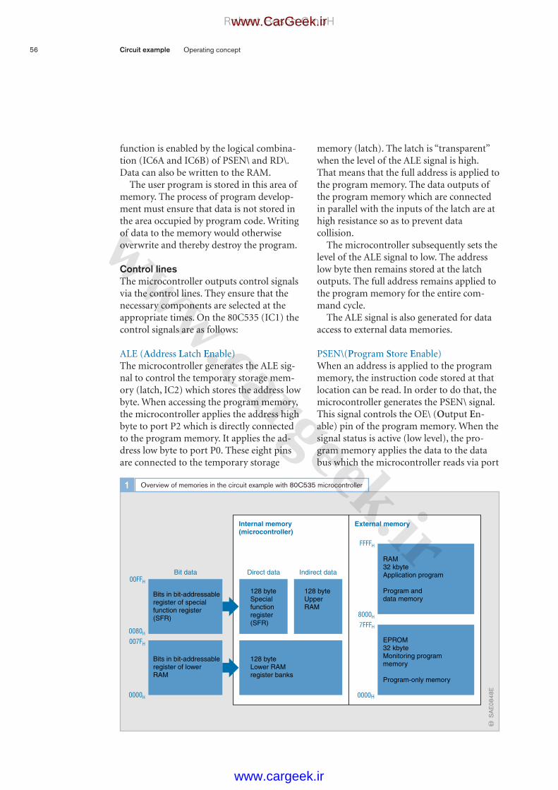
function is enabled by the logical combina-tion (IC6A and IC6B) of PSEN\ and RD\.Data can also be written to the RAM.
The user program is stored in this area ofmemory. The process of program develop-ment must ensure that data is not stored inthe area occupied by program code. Writingof data to the memory would otherwiseoverwrite and thereby destroy the program.
Control linesThe microcontroller outputs control signalsvia the control lines. They ensure that thenecessary components are selected at theappropriate times. On the 80C535 (IC1) thecontrol signals are as follows:
ALE (Address Latch Enable)The microcontroller generates the ALE sig-nal to control the temporary storage mem-ory (latch, IC2) which stores the address lowbyte. When accessing the program memory,the microcontroller applies the address highbyte to port P2 which is directly connectedto the program memory. It applies the ad-dress low byte to port P0. These eight pinsare connected to the temporary storage
memory (latch). The latch is “transparent”when the level of the ALE signal is high.That means that the full address is applied tothe program memory. The data outputs ofthe program memory which are connectedin parallel with the inputs of the latch are athigh resistance so as to prevent datacollision.
The microcontroller subsequently sets thelevel of the ALE signal to low. The addresslow byte then remains stored at the latchoutputs. The full address remains applied tothe program memory for the entire com-mand cycle.
The ALE signal is also generated for dataaccess to external data memories.
PSEN\(Program Store Enable)When an address is applied to the programmemory, the instruction code stored at thatlocation can be read. In order to do that, themicrocontroller generates the PSEN\ signal.This signal controls the OE\ (Output En-able) pin of the program memory. When thesignal status is active (low level), the pro-gram memory applies the data to the databus which the microcontroller reads via port
56 Circuit example Operating concept
Internal memory (microcontroller)
0000H
7FFFH
FFFFH
0000H
007FH
0080H
00FFH
Bits in bit-addressable register of special function register (SFR)
128 byteSpecialfunctionregister(SFR)
Direct dataBit data Indirect data
128 byteUpper RAM
Bits in bit-addressable register of lower RAM
128 byteLower RAM register banks
RAM32 kbyteApplication program
Program and data memory
EPROM32 kbyteMonitoring program memory
Program-only memory
External memory
8000H
Overview of memories in the circuit example with 80C535 microcontroller1æ
SA
E08
48E
Robert Bosch GmbH
www.cargeek.ir
www.CarGeek.ir
www.cargeek.ir

P0. The PSEN\ signal then switches back toinactive status and the data lines of the pro-gram memory revert to a high resistancelevel.
RD\To read the data memory (external RAM),the microcontroller must first access themodule. This is done in the same way aswhen reading the program memory. In thiscase too, the address low byte is temporarilystored in the latch.
The data is placed on the data bus by theRAM when the OE\ pin switches to the low-level signal. The OE\ pin is controlled by theRD\ signal. During this phase, the micro-controller reads the data bus via port P0.
Theoretically, the OE\ pin can be con-trolled directly by the RD\ signal from themicrocontroller. In this development circuit,however, the RD\ signal is combined withthe PSEN\ signal via a logic circuit (IC6A,IC6B) so that the RAM can also operate as aprogram memory.
WR\The address to which data is to be written is applied by the microcontroller to the ad-dress bus. The ALE signal is used to controlcopying of the data to the latch. The data issubsequently placed on the address bus. TheRAM copies the data on the data bus when alow-level signal is present at the WE\ (WriteEnable) pin. To that end, the microcon-troller activates the WR\ signal.
Reset\The Reset\ input (Pin 10) is required to reset the microcontroller to a defined status(input active at low signal level). When thedevelopment circuit is switched on, thistakes place automatically through the con-nection to capacitor C17 and its series resis-tor R1.
At the moment the power is switched on,capacitor C17 constitutes a short circuit.This is a physical property of the unchargedcapacitor. As a result, the Reset\ input of themicrocontroller is briefly connected to
ground. The microcontroller performs a re-set and reverts to the start of the monitoringprogram at address 0000H. After a certainperiod, the capacitor is sufficiently chargedfor the Reset\ input to adopt the high-levelstatus. The precise length of time dependson the rating of the capacitor and the seriesresistor R1.
In contrast to our example, there are alsomicrocontrollers on which the reset is activewhen the signal is high.
Serial interfaceThe connection between the PC and thecontroller is provided by an RS232 serialinterface.
The ports COM1 or COM2 can be used atthe PC end, using either a 25-pin or a 9-pinSUB-D connector. That and the data trans-mission rate are set in the PC program dur-ing the programming process.
On the development circuit there is a 9-pin SUB-D socket (X2) which is con-nected to the microcontroller serial interfacepins via the level converter MAX232 (IC5)(see description of IC5).
Circuit example Operating concept 57
Robert Bosch GmbH
www.cargeek.ir
www.CarGeek.ir
www.cargeek.ir
ProgrammingThe object code consists of an 8-digit binarynumber in the range 00H to FFH.
In all, the instruction set of the 80C535(IC1) extends to 111 instructions, of which 49 consist of a single byte, 45 consist of a two bytes, and 17 consist of a three bytes.
In the single-byte instructions, all informa-tion is contained in the “operation code”.
In the 2-byte instructions, the operationcode is followed by the operand which iseither a constant or an 8-bit address.
Such a series of numbers is, of course, diffi-cult to remember. That is why easily memo-rable abbreviations have been devised torepresent the binary operation codes.
Example:“Move register R0 to accumulator” is a sin-gle-byte instruction. It transfers the contentsof register R0 to the accumulator (A) – themicrocontroller’s computation register. Inbinary notation, that instruction reads thus:1110 1000B (which corresponds to E8H). Theabbreviated form of the instruction is “MOV A,R0”. This method of representingthe commands by mnemonics, i.e. easilymemorable abbreviations, is referred to asassembly language. These mnemonics haveto be translated into operation code by aprogram called an assembler.
A particular feature of the mnemonics isthe order of the operands. The instruction isfollowed first by the destination byte andthen the source byte.
“MOV R0, #01” is an example of a 2-byteinstruction. It instructs the CPU to transferthe numerical value 01H to the register R0(direct addressing).
When the CPU reads the operation code“MOV R0” it knows that the next byte readfrom the program memory is also part ofthe instruction.
Example program for “moving lights”The example program in Figure 1 producestwo moving-light sequences. A series ofLEDs is connected to the output channels ofeach of the ports P4 and P5. These LEDslight up when the logical 1 signal is presentat the corresponding pin. The time loop thatdetermines the speed of the moving lightcan basically be “set” by means of the regis-ters R2 and R3.
Program sequenceThe example program starts at the address8000H. That is the lowest memory address inthe RAM, which in this case is being ad-dressed as a program memory. In order forthe user program to be run, the monitoringprogram must jump to that location.
InitialisationThe initialisation process writes initial datato the registers. This means that the pro-gram starts with defined data.
The first instruction is a transferinstruction. The 8-bit constant with thevalue 0000 0001B (01H) is loaded into the 8-bit register R0. The hash symbol, #, indi-cates that the operand is a numerical valueand not an address. Since this instruction isa 2-byte instruction, it is stored at the loca-tions 8000H and 8001H.
In the next step, the constant 1000 0000B (80H) is copied to the registerR1.
Main programThe next instruction is also a transfer in-struction. The contents of register R0 arenow transferred to the accumulator andfrom there to the port register P4. The firstLED then lights up.
Now the contents of the accumulator are“rotated” one place to the left and reloadedinto register R0. Thus, in the next cycle, theilluminated LED “moves” to the next posi-tion in the row of LEDs connected to P4.
58 Circuit example Programming
Robert Bosch GmbH
www.cargeek.ir
www.CarGeek.ir
www.cargeek.ir

The program next branches into the subrou-tine “time” which determines the speed ofthe moving-light sequence. It can bechanged by altering the value of R3 or bymultiple calling of the subroutine.
The sequence for the second row of LEDs isidentical (register R1 and port P5) except forthe fact that the value of the accumulator is“rotated” to the right. The two “movinglights” thus move in opposite directions.
The program concludes with the 3-byte in-struction “JMP 8004”. This tells the programto jump to the address 8004H. In otherwords is repeats itself indefinitely until it isstopped by external intervention.
In contrast to this example, programs onmotor-vehicle control units use an internaltimer for time-based functions which doesnot draw on the microcontroller’s CPUresources.
SubroutineA subroutine is called at the address 8009H.The program then continues from the ad-dress 8100H. This subroutine represents adouble-nested time loop.
The two registers R2 and R3 are loadedwith the constant FFH. R2 is then decre-mented (decreased by 1). If the contents ofthe register are then not equal to the value00H, the subroutine returns to the start ofthe inner nested loop. Once the value of theregister has reached 00H, the subroutinemoves on to its next instruction. The outerloop is then executed until the value of R3 is also 00H.
The instruction RET (Return) then sendsthe subroutine back to the main program.The main program is continued with theinstruction immediately following the onein which the subroutine was invoked.
The advantage of a subroutine is that itcan be invoked from any number of pointsin the main program.
Circuit example Programming 59
LED at port 4 LED at port 5
Example program for “moving lights”1
æS
AE
0849
E
Memory address Assembly language Remarksin RAM (Hex) instruction
(source code)
;Initialisation8000: MOV R0,#01 ;Load register R0 with the constant 01H
8002: MOV R1,#80 ;Load register R1 with the constant 80H
;Main program;1st moving light:
8004: MOV A,R0 ;Load contents of register R0 into accumulator A8005: MOV P4,A ;Output the contents of accumulator A at port 48007: RL A ;Rotate the contents of A one place to the left
;(e.g. 000 0001B becomes 000 0010B)8008: MOV R0,A ;Load contents of accumulator A into register R08009: LCALL 8100 ;Invoke the subroutine at address 8100H
;2nd moving light:800C: MOV A,R1 ;Load contents of register R1 into accumulator A800D: MOV P5,A ;Output the contents of accumulator A at port 5800F: RR A ;Rotate the contents of A one place to the right
;(e.g. 1000 0000B becomes 0100 0000B)8010: MOV R1,A ;Load contents of accumulator A into register R18011: LCALL 8100 ;Invoke the subroutine at address 8100H
8014: JMP 8004 ;Jump to address 8004H
;Subroutine “time” (approx. 0.13 s)8100: MOV R3,#FF ;Load register R3 with the constant FFH
8102: MOV R2,#FF ;Load register R2 with the constant FFH
8104: DJNZ R2,8104 ;Decrement (reduce by 1) R2, ;If R2 ≠ 00H go to address 8104H
8106: DJNZ R3,8102 ;Decrement (reduce by 1) R3, ;If R3 ≠ 00H go to address 8102H
8108: RET ;Return to main program
Robert Bosch GmbH
www.cargeek.ir
www.CarGeek.ir
www.cargeek.ir

The control unit (ECU) is the central pointfrom which the functions of an electronicsystem in a motor vehicle are controlled.For that reason, extremely high demands inrespect of quality and reliability are placedon ECU development.
Overview
An electronic system consists of sensors andsetpoint generators, an ECU and actuators(Fig. 1).
The sensors detect the operating parame-ters of the electronic system (e. g. wheelspeed, engine temperature, ambient pres-sure). The setpoint generators register thesettings that the driver has specified withhis/her operating controls (e.g. by means ofthe air-conditioner switches). The sensorsand setpoint generators thus supply the in-put signals that are analysed and processedby the ECU.
Actuators (e.g. ignition coils, fuel injec-tors) convert the electrical output signalsinto physical variables.The process of developing an electronic sys-tem is made up of a number of stages, in
which the ECU development stage plays a decisive role. The following tasks are in-volved in the development of the ECU(Fig. 2): hardware development, function development, software development, and application.
RequirementsThe product specifications and the develop-ment specifications document the require-ments that a particular electronic system hasto meet. Those two documents form thebasis for the development process.
Product specificationsThe product specifications define the re-quirements from the point of view of thevehicle manufacturer. They describe thefunctions that the product concerned mustperform. They detail all requirements on thepart of the vehicle manufacturer with regardto the products and services to be supplied.The requirements specified should be quan-tifiable and measurable. The product specifi-cations thus define what means of perform-ing what task is to be provided.
The product specifications are not revisedduring the course of the developmentprocess.
Development specificationsFrom the requirements set down in theproduct specifications, the ECU manufac-turer draws up the development specifica-tions. The development specifications definehow and by what means the requirements areto be implemented (implementation specifi-cations).
The development specifications are the basisfor practical development of the ECU. Theyhave to be regularly reviewed and updated inconsultation with the vehicle manufacturerduring the course of the developmentprocess.
60 ECU development Overview
ECU development
Fig. 11 Sensors and
setpoint generators(input signals)
2 ECU3 Actuators4 Interface with other
systems5 Diagnosis interface
42
1
3
5
Components of an electronic system1
æU
AE
0734
Y
Robert Bosch GmbH
www.cargeek.ir
www.CarGeek.ir
www.cargeek.ir

ECU development Overview 61
Hardware development
Software development
Parallel PC interface
MAC
Control unit with electronic scannerunit (ESU)
Serial ESU interface
K lead (optional)
Development Specifications
Product Specifications
Quality Management
1.0
+
101101…
Function development(ECU function)
Application(data adaptation)
ECU development: Interrelationship of development tasks2
æS
AE
0909
E
Robert Bosch GmbH
www.cargeek.ir
www.CarGeek.ir
www.cargeek.ir

HardwareHardware is a generic term for the physical(i.e. tangible) components of a systemwhether mechanical (e.g. heat sink, casing)or electronic (e.g. microcontroller, memorymodules, output modules). This applies tothe components both individually and col-lectively.
The hardware of the ECU electrically pro-cesses the signals received from the sensorsand passes them onto the “processor core” ofthe control unit for further processing. Out-put modules amplify the control signals sothat the actuators can be operated with therequired electrical power.
The task of hardware development (Fig. 2) isto design and produce an ECU that meetsthe requirements arising from the develop-ment specifications.
ECU functionsThe control unit’s job is to analyse the inputsignals and to control the actuators so thatthe system operates according to its in-tended purpose. The overall behaviour ofthe system can be broken down into a num-ber of separate functions (e.g. for gasoline-engine management system: control of en-gine idling speed, exhaust emission levels,radiator fan, etc.). And even with today’sstate-of-the-art ECUs, the apparentlystraightforward control of the radiator fan is dependent upon a whole range of inputvariables. It is not sufficient merely to switchthe fan on when the engine is hot, and offagain when it has cooled down. Further-more, every vehicle manufacturer has itsown ideas as to exactly how this unit shouldoperate.
Function development (Fig. 2) involves theimplementation of the engine manufac-turer’s specifications, and the drawing up ofthe function descriptions which describe theECU functions down to the very last detail.Those documents form part of the develop-ment specifications.
SoftwareSoftware is a generic term for the total of theprograms and data stored in the memory ofa computer-controlled system.
The central element of an ECU that per-forms a function in a motor vehicle is themicrocontroller. It runs the program storedin the program memory. That program rep-resents the functions of the ECU in the formof program code.
The process of software development (Fig. 2)converts the requirements arising from thefunction descriptions into a program. Themachine code thus produced is entered inthe program memory of the ECU. To sim-plify the process of writing a program, pro-gramming languages are used. The increas-ing complexity of electronic systems makesthe use of high-level programming lan-guages (such as the language C) absolutelyessential. Software development is alsoassisted by simulation tools.
Data adaptationThe behaviour of an electronic system doesnot depend solely on the ECU program. Adecisive role is also played by the data storedin the memory along with the programcode. An example of such data in the case ofan engine ECU would be the ignition timingmap, which specifies the optimum ignitiontiming from the point of view of fuel con-sumption and emission levels for a range ofengine operating conditions (engine speedsand loads/torques). Such data is engine-spe-cific. For that reason, it has to be calculatedand adapted during the process of develop-ment of the vehicle. Adaptation of the datato the engine in this way is the task of theapplication stage (Fig. 2).
62 ECU development Overview
Robert Bosch GmbH
www.cargeek.ir
www.CarGeek.ir
www.cargeek.ir

Quality managementQuality assurance measures accompany theentire development process, and subse-quently the production process as well. Onlyin that way can consistent quality of the endproduct be guaranteed. The quality require-ments placed on safety-related systems (e. g.ABS) are particularly strict.
Quality assurance systemsAll elements of a quality management sys-tem and all quality assurance measures haveto be systematically planned. The varioustasks, authorities and responsibilities are de-fined in writing in the quality managementhandbook. International standards such asISO 9001 to 9004 are also adopted.
In order to regularly monitor all elements ofa quality management system, quality auditsare carried out. Their purpose is to assessthe extent to which the requirements of thequality management system are being fol-lowed and the effectiveness with which thequality requirements and objectives arebeing met.
Quality assessmentOn completion of specific stages in the de-velopment process, all information availableup to that point about quality and reliabilityis subjected to a quality assessment and anynecessary remedial action initiated.
FMEAFMEA (Failure Mode and Effects Analysis)is an analytical method for identifying po-tential weaknesses and assessing their signif-icance. Systematic optimisation results inrisk and fault cost reduction and leads toimproved reliability. FMEA is suitable foranalysing the types of fault occurring onsystem components and their effects on thesystem as a whole. The effect of a fault canbe described by a causal chain from point oforigin (e.g. sensor) to system (e.g. vehicle).
The following types of FMEA are distin-guished: Design FMEA: assessment of the design of
systems for compliance with the specifica-tions. It also tests how the system reacts inthe event of design faults.
Process FMEA: assessment of the produc-tion process.
System FMEA: assessment of the interac-tion of system components.
FMEA assessments are based on theoreticalprinciples and practical experience.
Example: a direction indicator fails. The ef-fects in terms of road safety are serious. Thelikelihood of discovery by the driver is small,however, since the indicator is not visiblefrom inside the vehicle. As a means of mak-ing the fault obvious, the rate at which theindicators flash must be made to change ifan indicator fails. The higher flashing rate isdiscernible both visually on the instrumentcluster and audibly. As a result of this modi-fication, the effect of the fault can bereduced.
ReviewThe review is an effective quality assurancetool in software development in particular.Reviewers check the compliance of the workproduced with the applicable requirementsand objectives.
The review can be usefully employed as ameans of checking progress made even atearly stages of the development process. Itsaim is to identify and eliminate any faults atas early a point as possible.
ECU development Overview 63
Robert Bosch GmbH
www.cargeek.ir
www.CarGeek.ir
www.cargeek.ir

Hardware developmentThe complexity of electronic systems hasseen a continuing increase in the past years.This tendency will continue in the future,and it will only be possible to master suchdevelopments by applying highly integratedcircuits. The call for small dimensions for allsystem components places further exactingdemands on the hardware developmentprocess.
Efficient and cost-effective hardwaredevelopment is now only possible by usingstandard modules that are produced in largenumbers.
Project starting pointA schematic diagram sets out all the func-tions that are to be performed by the ECUbeing developed. From that point, the fol-lowing aspects can be clarified: definition of hardware required, cost estimate for the hardware, extent of development work required, and cost of tools.
Hardware design prototypesOnce the project is underway, hardware de-sign prototypes are produced and subjectedto quality tests. These design prototypes maybe one of four categories representing suc-cessive stages along the road to the final pro-duction ECU. Each prototype category isbased on its predecessor and is designed fora particular purpose in each case.
‘A’ prototypeThe ‘A’ prototype is derived from an existingor modified ECU or a development circuitboard. Its range of functions is limited. Itstechnical function is largely in place but the‘A’ prototype is not suitable for continuoustesting. It is a function prototype that is usedfor initial trials and to confirm the basic via-bility of the design.
‘B’ prototypeThe ‘B’ prototype includes all circuit compo-nents. It is a trial prototype that is used to
test out the full range of functions and thetechnical requirements. At this stage it isready for continuous testing in prototypevehicles.
The connection sizes and ECU dimen-sions are as required for final production. Itmay be, however, that not all of the vehiclemanufacturer’s specifications are satisfied atthis stage, perhaps because different materi-als have been used, for instance.
‘C’ prototypeThe ‘C’ prototype is the approval prototypeon which the vehicle manufacturer’s tests for “technical approval” are performed. Thisversion of the ECU must reliably conform to all specifications. On successful approvalof the product, the development process iscomplete. As far as possible, ‘C’ prototypesare produced using full-production toolsand production methods as close as possibleto full series production.
‘D’ prototypeThe ‘D’ prototype is the pilot-series prototypewhich also carries the full-production iden-tification plate showing the version number.‘D’ prototypes are fitted in pilot-series vehi-cles for large-scale vehicle trials. This versionof the ECU is produced using volume-pro-duction methods and is fitted and tested un-der volume-production conditions. It is theversion with which the reliability of produc-tion is verified.
64 ECU development Hardware development
Robert Bosch GmbH
www.cargeek.ir
www.CarGeek.ir
www.cargeek.ir

PreparationsThe preparations for the ‘B’ prototype startfrom the beginning of the project and in-volve definition of connector pin assignment, definition of the casing design, ordering and developing new circuit
modules (function groups), producing the circuit diagram, defining the components (only approved
components may be included, or inclu-sion must be subject to approval).
When selecting the circuit modules (e.g.knock-sensor analyser circuits integrated inan IC), developers check whether existingcircuits – with modifications if necessary –can be used. If not, new modules have to bedeveloped.
Circuit diagram and components listA CAD (Computer-Aided Design) system isused to create the circuit diagram (Fig. 1 a)and the list of all components used. Thecomponents list also details the followinginformation for each component: its size, its pin assignment, its casing design, and the supplier and terms of supply.
LayoutA circuit-board layout (Fig. 1 b) is requiredfor production of the circuit board. It showsthe positions of the conductor tracks andthe connector pins.
The layout is produced on a CAD system.The process starts by taking the circuit-dia-gram data and converting it. The compo-nent connection schedule (list of connec-tions between components) then producedshows how the various components are con-nected to each other. From this componentconnection schedule and the CAD data forthe components (size and connector pin as-signment) the layout can then be produced.
ECU development Hardware development 65
Fig. 1a Circuit diagramb Layoutc Circuit-board
productiond Prototype
constructione Testing
GND
GND
GND
IC7
VCC
+VCCVCC
IC7A1
2
3
IC7C89
10
IC7B4
5
6
IC7D111213
GND
D1
R2C10
S2
C7
GND
a
b
c
d
e
Hardware development process1
æN
AE
0912
Y
Robert Bosch GmbH
www.cargeek.ir
www.CarGeek.ir
www.cargeek.ir

There are specific criteria that have to betaken into account in the creation of thelayout. In connection with the positioning of components these can include thefollowing considerations: the power loss from specific components
(possibilities for heat dissipation), EMC (electromagnetic compatibility)
effects, convenient positioning of components in
relation to connectors, observance of restriction zones
(component size), ease of fitting of components by auto-
mated production machinery, accessibility of testing points, and space requirements for testing adaptors.
Circuit boardThe layout data can be used to produce filmsfor manufacture of the printed-circuit board(Fig. 1 c). The films are used to photographi-cally expose the blanks (which are coveredwith a light-sensitive coating) and then de-velop and etch them. The individual layersof multilayer printed-circuit boards areplaced on top of one another and hardened.
Finally, the component print, the solderresist and a carbon lacquer are applied to thecircuit board.
Prototype constructionThe finished circuit board has to have thecomponents mounted on it (Fig. 1 d). In thecase of prototype products, this is part of theprocess of prototype manufacture. Becauseof the miniaturisation of components andthe high degree of integration on the printedcircuit, even prototypes have to have theircomponents fitted by machine. The machineis controlled by the CAD layout data.
Following fitting of the components, theirconnections are soldered. There are twoalternative soldering methods: wave soldering and reflow soldering.
Testing the finished circuit boardElectrical testingOnce all components have been fitted andall connections soldered, the circuit boardmust be tested. To this end, electrical testingsequences are defined which run on a com-puter. These automatic tests check that allcomponents are fitted and that the circuitfunctions properly.
ThermographicsThermographic images of the printed circuitshow the heat generated by the componentsduring operation (Fig. 2). Different temper-ature ranges appear on the film as differentcolours. In this way, components that aretoo hot can be identified. The informationobtained is incorporated in the list of modi-fications between the ‘B’ and ‘C’ prototypes.Changes to the circuit layout (e.g. heat-dissi-pation through-contacting) can reduce theamount of heat generated.
66 ECU development Hardware development
Fig. 2Engine control unitPower supply voltage U = 14 VIdling speed n = 1000 rpm
62°C 58°C 63°C 71°C
Thermographic image of a printed-circuit board2
æS
AE
0910
Y
Robert Bosch GmbH
www.cargeek.ir
www.CarGeek.ir
www.cargeek.ir

Electromagnetic testingThe electromagnetic fields created on thecircuit board can be scanned with a mag-netic field detector (Fig. 1 e). The readingsare analysed on a PC. Different fieldstrengths show up as different colours. Ifnecessary, modifications to the circuit layouthave to be made and additional componentsfitted that reduce the magnetic field or makethe ECU immune to interference.
These tests are performed on the ‘B’ proto-type so that the necessary modifications canbe incorporated in the ‘C’ prototype.
EMC testsReadings taken in the EMC testing cell ortesting chamber (Fig. 3) test the ECU re-sponse to external and internal sources ofelectromagnetic interference. Measurementsare taken both with the ECU fitted in thevehicle (in-situ tests) and in the laboratory(e. g. stripline method).
The difficulty with the in-situ tests is thatthey cannot be carried out until develop-ment of the vehicle and all its electronic sys-tems is at a very advanced stage. If the EMCcharacteristics are found to be unsatisfactoryat this stage, the scope for modifications isthen severely limited. For this reason, labora-tory testing is extremely important because itpermits potential problems to be identifiedon the hardware prototypes at an early stagein the process.
The EMC readings are taken at a variety offrequencies and with a range of electric fieldstrengths. The immunity of the output sig-nals (e.g. ignition signals, fuel injection sig-nals) to external interference is examined aswell as the level of interference generated bythe unit itself.
ECU development Hardware development 67
2
3
1
Vehicle in the EMC testing chamber3
æS
AE
0911
Y
Robert Bosch GmbH
www.cargeek.ir
www.CarGeek.ir
www.cargeek.ir

The manufacture of microelectronic com-ponents and circuits demands ultra-highprecision as well as extremely high stan-dards of cleanliness in the various stages ofproduction. Even the minutest speck of dirtcan irreparably damage a circuit.
Semiconductor components
Most semiconductor components are madeof silicon. The raw material is SiO2 (quartz).It occurs naturally in large quantities as rockcrystal or silica sand. It is used to makemonocrystalline cylinders or rods of ex-tremely pure silicon with a diameter ofbetween approx. 50 mm (2″) and 300 mm(12″). The most common diameters are150 mm (6″) and 200 mm (8″).
During the production of the crystals, theyare given a precise conductivity specified bythe component manufacturer (basic dop-ing). The cylindrical crystal is sliced intodiscs roughly 0.3 ... 0.7 mm thick which arethen smoothed and polished. These discs arereferred to as wafers.
The process of producing the semiconduc-tor components starts with these siliconwafers (Fig. 1). The value-added chain fromthe raw material to the end product showsan extremely high rate of value growth: sili-con in the form of silica sand costs about1 euro per kg, but by the time it has becomea finished microprocessor it can be worth upto 1 million euro per kg.
A large number of identical circuits(chips) is created on each wafer and thosecircuits are then separated by mechanicalmeans. Before separation, however, the chipsare tested to make sure they match the elec-trical specifications. Any unusable chips aremarked and then discarded once separated.Only the usable chips are assembled, i.e.cemented, bonded, encased, sealed andpassed on for final testing (Figs. 1 and 3).
Doping processDoping involves introducing impurities witha known electrical effect into the semicon-ductor crystal at specific points and in pre-cisely defined concentration levels using re-producible methods. Doping techniques arethe fundamental processes of semiconductortechnology. The guiding parameters are con-centration profile, penetration depth, sur-face concentration and planar parallelity ofthe doping-material fronts.
Doping during crystal growthWhile the crystal is being grown, phos-phorus can be added to the silicon melt as adoping material. As the monocrystal forms,the phosphorus atoms become fixed in the
68 Manufacture of semiconductor components and circuits Semiconductor components
Manufacture of semiconductor components and circuits
Cutting, smoothing and polishing the wafer
After controlled doping process: multiple identical semi-conductor elements
Testing and marking of unusable chips
Separation into individual chips
Assembly, cementing, bonding
Encasing, sealing
Stages in the manufacture of semiconductor components
1
æS
AE
0078
E
Robert Bosch GmbH
www.cargeek.ir
www.CarGeek.ir
www.cargeek.ir

silicon crystal, giving it n-type conductingproperties.
Manufacturers of semiconductor compo-nents buy their raw material in the form ofwafers that have been pre-doped accordingto precisely defined specifications.
Doping by diffusionAt high temperatures, the doping materialcan diffuse into the silicon crystal. The effectis achieved by creating a specific concen-tration level of the impurity atoms at thesurface of the wafer. The difference in con-centration causes the doping atoms to dif-fuse into the silicon wafer.
The process involves placing between 50 and 200 wafers in a kiln together and exposingthem to boron or phosphorus compoundvapours at temperatures of around 1000 °C.Boron produces p-type regions while theeffect of phosphorus is to create n-type re-gions. Surface concentration levels, tempera-ture, and time, are the parameters that de-termine the penetration depth of the dopingmaterial.
Doping by ion implantationIn this process, the atoms of a gaseous dop-ing material are first of all ionised in a vac-uum and then accelerated by a high voltage(up to 300 kV) so as to be “catapulted” intothe semiconductor. This allows particularlyprecise control of concentration level andlocalisation of the implanted material.Embedding of the implanted atoms andrestoration of the crystal lattice requiressubsequent thermal treatment.
EpitaxyThis doping method creates a monocrys-talline doped semiconductor layer a fewmicrometres thick on a monocrystallinesubstrate. If gaseous silicon tetrachlorideand hydrogen are passed over silicon wafersheated to around 1200 °C in a quartz tube,the vapour breaks down and silicon is de-posited at a rate of about 1 µm/min, form-
Manufacture of semiconductor components and circuits Semiconductor components 69
Design
Photomasks
Wafer testing
Chip assembly
Final testing
Oxidising Removal
Cutting Doping
Design transfer byphotolithography
e.g. planar process
Siliconwafers
Process of manufacturing semiconductorcomponents
3
æN
AE
0079
E
50 m
Microstructure of a microchip with bondedconnections
2
æU
AE
0870
Y
Robert Bosch GmbH
www.cargeek.ir
www.CarGeek.ir
www.cargeek.ir
ing a monocrystalline layer. If a definedquantity of doping impurity is added to thegas flow, an epitaxial layer is created whoseelectrical conductivity and conduction typediffers fundamentally and abruptly fromthat of the substrate.
Photolithography and the planar processIn the photolithography process, the patternof the component design is transferred tothe wafer by using metal screens. When thedesign has been created, the data for pro-ducing the screen is saved onto a storagemedium (e.g. magnetic tape or CD). It isthen used to control a photographic expo-sure device that transfers the design patternto photographic plates. This pattern is sub-sequently reduced by optical means to theactual size for the application and copiedonto metal screens on which it is repeated asmany times as will fit onto the size waferbeing used.
As this method can be used for structuresthat are many times smaller than the wave-length of the light used, it will continue tobe used in the future. The size of the small-est achievable structures depends on thewavelength of the light source. UsingUV lasers, photolithographic methods havealready produced structures as small as0.08 µm in the laboratory (by comparison, ahuman hair has a diameter of 40 ... 60 µm).
Even smaller structures can be producedusing other methods such as X-ray or elec-tron-beam lithography. However, thosemethods are substantially more expensive asthey can only “expose” one IC at a time onthe wafer. For that reason, they are only usedin special cases.
Silicon wafers are easily oxidised by oxygenor water vapour. The oxide layer thus createdprevents penetration by the doping atoms inthe doping process. In the planar process,holes are created in the oxide layer so thatwhen the wafer is doped, localised areas ofn-type and p-type material are created.
The wafer is coated with a special lacquerand then exposed to light while covered witha metal screen. Following developing, theareas of the lacquer coating previously cov-ered by the screen and the oxide layer belowit can be removed by etching. The position,size and shape of the holes thus createdmatch precisely the specified design. In thesubsequent doping process in the diffusionfurnace (Fig. 4) or by ion implantation, im-purities which have a known electrical effectsuch as boron or phosphorus pass throughthose holes in the oxide layer into the sili-con, thereby creating n-type or p-type re-gions in the desired locations. Afterwards,the oxide layer is removed again and thewafer is ready for the next stage in themanufacturing process.
The photolithographic process and the dop-ing process are repeated as many times asrequired to produce the desired number oflayers of different conductivity on the semi-conductor component. In the case of com-plex integrated circuits, this may involve asmany as 20 or more separate manufacturingstages. In order to provide the electrical con-nections between the resulting functionalelements, the wafers are coated with alu-minum or copper and then the metal con-ductor track patterns are formed. Thisprocess too may involve the formation ofmultiple layers of metal, one above the other.
Completion of the wafer production processis followed by electrical testing (preliminarytesting) of the individual chips on the wafer.Chips that do not meet the specifications aremarked with coloured dots. The wafers arethen cut up into individual chips using adiamond cutting tool (Fig. 5). The func-tional chips are subsequently placed in metalor plastic casings and fitted with externalconnections (Fig. 6). After being hermeti-cally sealed or encased in plastic, they gothrough a final testing stage.
70 Manufacture of semiconductor components and circuits Semiconductor components
Robert Bosch GmbH
www.cargeek.ir
www.CarGeek.ir
www.cargeek.ir

Manufacture of semiconductor components and circuits Semiconductor components 71
Fig. 61 Base2 Chip3 Bonded connection
wire4 Connection pin
Wafers about to be placed in a diffusion furnace
4
1 2 43
Assembled microchip with connections prior to sealing
6
æN
AE
0075
Y
æN
AE
0871
Cutting the silicon wafer into individual chips5
æN
AE
0077
Y
Robert Bosch GmbH
www.cargeek.ir
www.CarGeek.ir
www.cargeek.ir

72 Manufacture of semiconductor components and circuits Micromechanics
Fig. 1a Production of a
diaphragmb Production of a holec Production of bars
and ridges
1 Etching screen2 Silicon
Fig. 2A Deposition and
shaping of thesacrificial layer
B Deposition of thepolysilicon
C Shaping thepolysilicon
D Removing thesacrificial layer
Fig. 31 Fixed electrode2 Gap3 Oscillating electrode
1 2 3
12 m
2 m
1
2
MicromechanicsMicromechanics is the name given to the pro-duction of mechanical components from semi-conductors (generally made of silicon) utilisingsemiconductor technologies. In addition to itssemiconducting properties, the mechanicalcharacteristics of silicon are made use of aswell. This makes it possible to create sensorswith the most minute of dimensions. The fol-lowing techniques are used:
Bulk micromechanicsThe silicon wafer material is removed up to thefull thickness of the wafer by anisotropic (alka-line) etching with or without electrochemicalresist. The material is etched away from thereverse side of the silicon layer (Fig. 1, item 2)in those areas where it is not protected by theetching screen (1). This method can be usedto create very small diaphragms (a) with typi-cal thicknesses of between 5 and 50 µm,holes (b) and bars and ridges (c), e.g. forpressure or acceleration sensors.
Surface micromechanicsThe base material is a silicon wafer on the sur-face of which miniature mechanical structuresare formed (Fig. 2). First of all, a “sacrificiallayer” is applied and shaped (A) using semi-conductor production processes (e.g. etch-ing). This is deposition-coated with a layer of polysilicon approximately 10 µm thick (B)which is then shaped by vertical etching usinga lacquer screen (C). In the final stage, thesacrificial oxide layer below the polysiliconlayer is removed using gaseous hydrogen fluo-ride (D). In this way, structures such as flexibleelectrodes (Fig. 3) for acceleration sensorscan be created.
Wafer bondingAnodic and seal glass bonding are methodsused to join wafers together by the action ofelectricity and heat or heat and pressure inorder, for instance, to hermetically seal a refer-ence vacuum or to protect sensitive structuresby placing a cap over them.
Structures producible using bulk micromechanics1
æU
AE
0696
-1Y
Surface micromechanics (stages of process)2 Surface micromechanics (structure details)3
æU
AE
0794
Y
æU
AE
0793
Y
a
b
c
A
B
C
D
Screen placed over wafer Etching Screen removed
Robert Bosch GmbH
www.cargeek.ir
www.CarGeek.ir
www.cargeek.ir

Conventional printed-circuitboardsThe printed-circuit board has become anelectronic component in its own right. It hasto have precisely defined electrical and me-chanical properties. In a motor vehicle, forexample it may be required to withstandtemperatures ranging from –40 ... +145 °C.The standards required in respect of EMC(electromagnetic compatibility), maximumcurrent capacity and complexity are becom-ing more and more demanding. And at thesame time, the circuit boards are continuallyexpected to become smaller and cheaper –in spite of shorter product life cycles.
The basic material – the baseboard – is glassfibre. It can be rigid or semi-flexible. Theconductor tracks on the surface are madefrom a thin layer of copper 12 ...70 µm thick(copper base). To protect it against corrosion,the surface of the copper is protected by acoating of tin alloy, gold or an organic surfacesealant, depending on the type of applica-tion.
DesignsDepending on the complexity of the circuit,printed-circuit boards may be made up of a
number of layers (Fig. 1). Circuit boardsused in motor vehicles consist of betweentwo and eight layers.
Single-sided circuit boardThe pattern of conductor tracks and soldereyes is only on one side of the baseboard (a).
Double-sided, non-interconnectedcircuit boardThere are patterns of conductor tracks onboth sides of the circuit board. However,those two circuits are not connected to eachother (b).
Double-sided, interconnected circuit boardThe conductor track patterns on each sideare interconnected by copper linings insidethe holes (c).
Multilayer circuit board In addition to the two outer layers (in thiscase the 1st and 4th layers), there are addi-tional conductor layers on the inside of thebaseboard (internal layers). Those conduc-tor layers may be electrically connected withone another. To that end, the relevant con-ductor layers are connected to the copperlinings inside the holes (d).
Manufacture of semiconductor components and circuits Conventional printed-circuits 73
Fig. 1Schematic diagram:conductor tracks areshown as raisedsurfaces
a One-sidedb Double-sided,
non-interconnectedc Double-sided,
interconnectedd Multilayer
1 Conductor track2 Solder eye3 Baseboard4 Hole5 Copper lining
a b
1 32
4
1 32
4
c d
1 32
4+51 2 1
1
1. layer2. layer3. layer
4. layer
32
4+52 1
Types of printed circuit board1
æS
AE
0872
E
Robert Bosch GmbH
www.cargeek.ir
www.CarGeek.ir
www.cargeek.ir

Production processPattern plating and panel plating have
become the established methods of manu-facturing printed-circuit boards (Fig. 2).
74 Manufacture of semiconductor components and circuits Conventional printed-circuits
Fig. 2The base material iscoated on both sideswith a copper film
Hole-pattern drilling
Chemical copper platingA conductive lining layer is formed inside the holes (2...5µm).
Photoresist application(coating, exposing, developing).
Solder-resist application (screen printing)
Protective coating application (e.g. gold (Ag), tin-lead alloy (SnPb))
Copper electroplating25 µm copper (Cu) deposited on the surface including the hole linings.
Hole-pattern drilling
Chemical copper platingA conductive lining layer is formed inside the holes (2...5µm).
Conductor-pattern etchingThe copper below the etching resist is not etched away.
Solder-resist application (screen printing)
Protective coating application (e.g. gold (Ag), tin-lead alloy (SnPb))
Photoresist removal ("stripping")
Etching-resist removal ("stripping")
Partial copper electroplating25 µm copper (Cu) deposited on the uncovered areas including the hole linings.
Photoresist application(coating, exposing, developing). This layer leaves the conductor tracks and solder eyes uncovered.
Etching resist electro-depositing10 µm tin-lead alloy (SnPb)or tin (Sn) deposited on the uncovered areas.
Conductor-pattern etchingThe copper below the etching resist is not etched away.
Photoresist removal ("stripping")
Manufacturing process for printed-circuit boards2
æN
AE
0873
E
Panel plating Pattern plating (tenting process) (subtractive process)
Robert Bosch GmbH
www.cargeek.ir
www.CarGeek.ir
www.cargeek.ir

Subsequent processingOnce the circuit board has been produced, ithas to be fitted with the circuit components.These subsequent processing stages alsodemand the highest quality standards so asto ensure reliable operation of the finishedproduct in the vehicle. There are two meth-ods of mounting the components on theboard – through-fitting and surface mount-ing.
Through-fitting methodWith the through-fitting method, the com-ponent connections are passed through theholes in the circuit board and then soldered(Fig. 3a).
Surface-mounting methodThe surface-mounting method SMT usesspecial electronic components whose con-nections lie flat against the surface of the cir-cuit board (Fig. 3b). Such components arereferred to as SMDs (surface mounted de-vices). Another advantage – in addition tothe greater component density achievable –is that the components can be fitted to thecircuit board fully automatically. The surfacemounting method is therefore becomingmore and more widely adopted. The com-ponent fitting machines used can achievework rates of more than 60,000 components an hour, increasing productivity as a result.
Production sequenceThere are various production systems thatare used in the subsequent processing ofcircuit boards and they are classified accord-ing to the spatial arrangement of the pro-duction equipment and the work areas. Thecategories distinguished are job-shop, pool,flow-shop and flow production.
The process described below is an exampleof flow production (Fig. 4). According to thestandard DIN 33 415, flow production in-volves “a process of operations organisedaccording to the flow principle in a rigidsequence, aligned to a particular spatialarrangement and tied to a cyclic timing
pattern”. Furthermore, the flow principle in-volves “arrangement of the individual workstations according to the order in which theoperations are performed”. This method isalso referred to as line production.
Production of the electronic circuits of anECU involves the following stages:
Basic materialsThe basic materials consist of printed-circuitboards that have not yet been fitted with cir-cuit components. Usually, one or more cir-cuit boards are arranged on a “panel” ofstandardised dimensions. After being fittedwith components, the circuit boards are cutout of the panel.
Manufacture of semiconductor components and circuits Conventional printed-circuits 75
Fig. 3a Through-fitting
methodb Surface-mounting
methodc Mixed mounting
1 Wired component2 Circuit board3 SMD4 Soldering point5 Cement
a
b
c
24
4
2
3
5
3
2
1
1
Component fitting methods for printed-circuit boards3
æU
AE
0469
-1Y
Robert Bosch GmbH
www.cargeek.ir
www.CarGeek.ir
www.cargeek.ir

Solder-paste applicationThe first stage is the application of solderpaste for the SMDs using a screen printingprocess. The solder paste is a mixture ofmetal powder, flux and other organic addi-tives. It is pressed through the spaces in theprinting screen onto the panel with the aidof a “scraper”.
SMD fitting (reflow side)An automatic component-insertion ma-chine presses the SMDs into the solder pasteapplied to the panel.
Reflow ovenThe panel passes through a reflow oven on aconveyor belt. The heat of the oven melts thesolder paste on the panel. This electricallyand mechanically connects the componentsto the pcb.
Position checkingThe camera of a vision system examines thesoldered connections (position checking sys-tem). Depending on the findings of the ex-amination, the panel may be diverted to arepair station or automatically moved on to the next stage of production.
Turning the circuit boardIn this stage, the circuit board is rotatedthrough 180 degrees so that the “underside”is facing upwards and can be worked on.The way in which components are fitted tothe underside depends on the nature of thesecond soldering stage.If the reflow/reflow method is used, theprocess described above is repeated.
If the alternative reflow/wave method isused, since the soldering method applieddiffers to that from the top side, the SMDsare fitted differently and a cementing stationis required.
Cementing station (underside)At the cementing station, cement spots arefirst of all applied in those positions on the“underside” where SMDs are to be placed.This is done using pipettes or a screen, simi-
lar to the procedure for applying the solderpaste. The cement holds the SMDs in posi-tion until they are soldered.
SMD fitting (underside)At succeeding stations along the assemblyline, the circuit components are placed onthe cement spots. On this side of the circuitboard, only components that are suitable forattachment by wave soldering can be fitted.
Cement hardeningIn order to prevent the components fallingoff during the soldering process, the cementis hardened in an oven.
Component checkingA visual component checking system checksthat all components are present and thatthey are in the correct positions on the un-derside of the circuit board. Non-compliantproducts are indicated and diverted to arepair station.
Turning the circuit boardThe circuit board is once again rotatedthrough 180 degrees, returning it to its origi-nal orientation.
Wired-component fittingThis stage involves fitting components thathave leads attached (e.g. large coils andconnectors) into ready-made holes (soldereyes) in the panel using the through-fittingmethod. They are subsequently soldered on the reverse side at the same time as theSMDs during the wave-soldering stage. Thewired-component fitting stage completes thecomponent fitting operations.
Wave solderingThe wave soldering stage solders the connec-tions of all SMDs and “wired components”on the underside. The wave solderingprocess involves the following three stages:1. Flux is applied to the underside of the
panel.
76 Manufacture of semiconductor components and circuits Conventional printed-circuits
Robert Bosch GmbH
www.cargeek.ir
www.CarGeek.ir
www.cargeek.ir

2. The panel then passes through a pre-heat-ing zone so that the components are notdamaged by the sudden increase in tem-perature in the subsequent stage.
3. The panel passes over a wave of liquid sol-der created by a jet. As it does so, the sol-der is deposited on the soldering points(pads) on the panel. The solder resist onthe circuit board prevents the solderattaching itself in the wrong places.
Position checkingAnother camera checks the finished solderedconnections. If faults are found, the panel ispassed to a repair station.
In-circuit testing (ICT)The purpose of the in-circuit test is to checkthat the electrical circuit is working prop-erly. The testing equipment is connected viaa testing adaptor and checks the compo-nents for correct function and electricalreadings.
CuttingThe individual circuit boards are now cutout of the panel using computer-controlledmachines.
Final assemblyIn the final-assembly stage, the circuit boardis fitted into the ECU casing.
Temperature testingThe finished ECU is subjected to very hightemperatures in order to test its ability towithstand extreme conditions. The testssimulate operation of the ECU in real condi-tions. In this way, component or solderingfaults can be detected.
Final testingBefore the ECU leaves the production line,it is subjected to a final test to make sure itperforms the functions required of it in ac-tual use.
Manufacture of semiconductor components and circuits Conventional printed-circuits 77
Turning the circuit board
Position checking
Final assembly
Cementing station
Turning the circuit board
In-circuit testing
Temperature testing
SMD fitting
Wired-component fitting
Cutting
Final testing
Position checking
Cement hardening
Wave soldering
Solder paste application SMD fitting Reflow oven
Stages in pcb manufacture using a flow production process and reflow/wave soldering (example)4æ
SA
E08
74E
Robert Bosch GmbH
www.cargeek.ir
www.CarGeek.ir
www.cargeek.ir

Film and hybrid circuitsFilm circuitsIn film integrated circuits, passive circuit el-ements (usually conductor tracks, insulationand resistors, but also capacitors and induc-tors) are applied to a base (substrate) in lay-ers. The advantages of these circuits are: fine structures (up to approx. 10 µm) with
high element density, and good high-frequency characteristics.
Those advantages are counterbalanced byrelatively high production costs.
The thickness of the films originally gaverise to the terms “thin-film circuit” and“thick-film circuit”. Classification is nowbased on differences in the method of pro-duction.
Thin-film circuits With thin-film circuits, the films are appliedto glass or ceramic substrates using vacuum-coating processes.
Thick-film circuits For thick-film circuits, the preferred methodof manufacture involves application of thefilms to ceramic substrates by screen print-ing processes followed by firing.
Ceramic multilayer substratesCeramic multilayer substrates are made upof unfired ceramic foils onto which conduc-tor tracks are applied by screen printingmethods. Several such foils are then com-bined to form a multilayer laminate which is fired at 850 ... 1600 °C so that it becomes asolid ceramic body with integral conductorchannels. A typical hybrid substrate consistsof four or five layers. Particularly highwiring densities can be achieved with LTCC(low-temperature cofired ceramic) line-linesubstrates.
To make the electrical connections betweenlayers, holes are punched in the individualfilms and filled with metal paste. Thoseholes are referred to as so-called “vias”. By
using suitable material systems, resistors andcapacitors can also be integrated. The wiringdensities of these circuits is considerablygreater than with thick-film circuits.
Hybrid circuitsHybrid circuits are integrated film circuitswith additional discrete components such ascapacitors and integrated semiconductorcircuits (ICs) that are attached by solderingor cementing. The use of unpacked semi-conductor chips, to which the connectionsare made by bonding, or SMDs makes highcomponent densities possible. Extremelysmall hybrid ECUs (microhybrids) can bemade by using ceramic multilayer sub-strates. The advantages of these circuits are: high permissible installation temperatures
due to their good heat dissipation proper-ties,
compactness of design combined withgood shock resistance, and
good resistance to mediums.
Hybrid circuits are therefore particularlysuited to use in telecommunications systemsand for automotive applications where theycan be found in ABS, traction control, ESP,transmission control and engine-manage-ment ECUs (engine-mounted).
Figure 1 shows the basic stages in the pro-duction of a hybrid-circuit substrate. Thetapes are punched with holes for the vias foreach separate wiring layer and the holes arethen filled with silver paste (Fig. 2a). Screen-printing stations print the conductor tracksonto the film. The various layers are alignedwith each other, laminated and then fired at890 °C. A specially controlled sintering pro-cess keeps the ceramic firing to within toler-ance limits of roughly 0.03 %. This is impor-tant for the packing density. The circuit’s re-sistors are printed on the reverse side of thesubstrate and fired (Fig. 2b).
For bonding on the top side, the surfacesare finished using a plating process adaptedto the LTCC. The spacing of the microcon-troller contacts (bond land grid on the
78 Manufacture of semiconductor components and circuits Film and hybrid circuits
Robert Bosch GmbH
www.cargeek.ir
www.CarGeek.ir
www.cargeek.ir

substrate) ranges from 450 to 260 µm. Thecomponent connections are bonded using32-µm gold wire and 200-µm aluminumwire.
Alongside the electrical vias, there are alsothermal vias with a diameter of 300 µm foroptimum cooling of ICs with high powerlosses. The effective thermal conductivity ofthe substrate can thus be increased fromapprox. 3 W/mK to 20 W/mK.All components are cemented with conduc-tive cement. There are two methods used forfinal assembly of the finished hybrid.
Method 1: the finished hybrid is cemented tothe steel panel of the casing using heat-con-ducting cement and connected to the glassfeed-through for the connector usingbonded 200-µm aluminum wire. The casingis then hermetically sealed.
Method 2: the finished hybrid is cemented to the aluminum casing using heat-conduct-ing cement and connected to the plastic-en-cased connector pins using bonded gold or300-µm aluminum wire. Before the cover iscemented in place, a gel is applied to protectthe circuit.
Manufacture of semiconductor components and circuits Film and hybrid circuits 79
Fig. 2a Inner layerb Reverse side with
resistorsc Top side inside ECU
1 Conductor track2 Via3 Resistor4 Microcontroller5 Bonded wire
Fig. 11 Unfired glass-ceramic
film2 Punching of holes,
filling with conductorpaste and printing ofconductor tracks
3 Aligning and stacking(laminating)
4 Sintering5 Printing of resistors
(reverse side), firingand plating of thebonding pads (topside)
6 Fitting of componentsand wire bonding
1
2
34
56
Production sequence of a microhybrid substrate1
æS
AE
0875
Y
2 cm
5 m
m
1
a b c
2 cm
13
5
4
2
Example of a hybrid circuit (sections)2
æN
AE
0876
E
Robert Bosch GmbH
www.cargeek.ir
www.CarGeek.ir
www.cargeek.ir

This glossary provides a quick guide to themost important automotive microelectron-ics terms.
An arrow pointing to a term printed initalics (e.g.p semiconductor) indicates thatthis italicised term is also explained in thisglossary.
A
Analog circuitp Electronic circuit withwhich analog signals are processed – asopposed to p digital circuit. Analog signalsare infinitely variable within a specific range.Examples: battery voltage, speedometerdisplay.
Avalanche breakdown: Sudden increase inthe number of p charge carriers resultingfrom the release of bound electrons from thecrystal lattice of a p semiconductor in thep space-charge zone caused by a high-strength electric field (p avalanche effect).
Avalanche effect: see p avalanche breakdown
B
Binary code: Information encoded in theform of binary numbers and therefore con-sisting of a sequence of the digits 0 and 1.
Bipolar transistor:p Transistor with threeregions of differing conductivity (p p-typesemiconductor and p n-type semiconductor).It is constructed either as a p-n-p or n-p-ntransistor. The terminals are called emitter(E), base (B) and collector (C).
Bit: Contraction of binary digit. A singledigit in p binary code
Breakdown voltage: reverse voltage at a p p-n junction above which a small increasein voltage brings about a large increase inthe p reverse current.
Bus: Connection linking the elements of ap digital circuit and consisting of a singlelead (serial bus) or multiple leads (parallelbus). A bus can connect up a large numberof separate elements with different functionsbut with electrically identical interfaces.A parallel bus transmits all bits of a data“word” simultaneously (one lead for eachbit). A serial bus transmits the bits sequen-tially (one after the other).
Byte: Coherent group (“word”) of eightp bits.
C
Capacitance: Property of a capacitor whichindicates how much electrical charge – andtherefore electrical energy – it can storewhen a specific voltage is applied.
CCD: Abbreviation for p charge-coupleddevice.
Central processing unit (CPU): Main oper-ating unit of a pmicrocontroller.
Charge-coupled device (CCD): Silicon im-age sensor in which incident light striking atransparent electrode releases p charge car-riers in proportion to the light intensity andexposure time. The charge carriers collect ina Si-SiO2 boundary layer (“potential well”).
Charge carrier: Carrier of electric charge,usually of a single elementary unit of charge.Free electrons and anions are examples ofnegative charge carriers.p Lattice defects(holes), cations and protons are examples of positive charge carriers.
Chip: Basic building block of microelec-tronic circuits. Base material is a monocrys-talline block of semiconductor material,primarily silicon.
80 Glossary and tables for automotive microelectronicsonventional Printed Circuits
Glossary and tables for automotivemicroelectronics
Robert Bosch GmbH
www.cargeek.ir
www.CarGeek.ir
www.cargeek.ir

Circuit diagram: Diagram illustrating themanner in which the individual electroniccomponents of a p circuit are electricallyconnected to each other.
Circuit, electrical: Combination of electricalor electronic components forming a self-contained functional unit. Circuits are alsoreferred to, both collectively and individu-ally, as p hardware.
Circuit layout: Arrangement of conductortracks and components on a printed circuit.
Clock-pulse generator: Circuit that gener-ates a timing pulse of a fixed frequency forsynchronising all operations in a pmicro-computer.
Closed-loop control: Method of controlcharacterised by a closed control loop. Theactual value of a variable is continually com-pared with its specified value. As soon as adifference is detected between the two, areadjustment is made to the setting of theactuator (output variable).
Communication: Exchange of data betweenelectronic components.
Conductivity: Reciprocal of resistance(1/Ω = A/V).
Conductor: Material with high electricalp conductivity due to its large number offree p charge carriers. Metals are the bestconductors.
CPU: Abbreviation for p central processingunit.
D
Degree of integration: Number of func-tional elements per p chip.
Diffusion: Migration of atoms, molecules orp charge carriers from a region of high tem-perature or concentration to a region of lowtemperature or concentration. This effect isutilised in the p doping of silicon waferswith impurities.
Diffusion voltage: Voltage created by thep diffusion of p free electrons and p holes atthe p p-n junction of a p semiconductor.
Digital circuit: Electronic circuit with whichdigital signals are processed – as opposed top analog circuit. Digital signals are in theform of a series of discrete pulses ratherthan infinitely variable characteristics. Ex-ample: digital clock.
Diode: Component with a p p-n junctionand two connections – one to the p-typeregion and one to the n-type region.
Discrete active component: Active compo-nent with fewer than 100 individual func-tions on a single p chip.
Doping: Controlled introduction of impuri-ties with known electrical effects into high-purity semiconductor crystals with the aimof producing p free electrons to create anp n-type semiconductor or p holes to createa p p-type semiconductor.
DRAM: Abbreviation for p dynamic ran-dom-access memory.
Dynamic random-access memory (DRAM):Volatile short-term memory (DRAM =Dynamic p RAM) which allows direct ac-cess to any memory location and which does not retain its contents when the powersupply is switched off.
Glossary and tables for automotive microelectronics 81
Robert Bosch GmbH
www.cargeek.ir
www.CarGeek.ir
www.cargeek.ir

E
EEPROM: Abbreviation for ElectricallyErasable Programmable Read-Only Mem-ory, i.e. a p read-only memory that can beelectrically erased and reprogrammed.EEPROM is also called E2PROM.
Epitaxy: Method of p doping silicon wafersin which a gaseous mixture of silicon tetra-chloride, hydrogen and doping impurities is passed over wafers heated to around1200 °C. An epitaxial layer is created, theelectrical conductivity of which differs sig-nificantly from that of the p substrate.
EPROM: Abbreviation for ErasableProgrammable Read-Only Memory, i.e.a p read-only memory that can be erasedusing UV light and then reprogrammed.
F
FET: Abbreviation for p field-effect transis-tor.
Field-effect transistor (FET):p Transistor inwhich the current flowing through a con-ductive channel is controlled by an electricfield that is created by a voltage applied tothe control electrode.
Flash EPROM: Programmable p read-onlymemory. Often simply called a “flash”.
Free electron: Electron that is unattached toan atom and can therefore move freely.
H
Hardware: Generic term for the physical(tangible) components of an electronic sys-tem. It includes the mechanical as well as theelectronic components and the combinationof them.
Hole: See p lattice defect.
Hybrid circuit board:p Integrated circuit inwhich the conductor tracks and the passiveelements are printed directly onto a ceramichybrid substrate. Hybrid circuit boards areparticularly suited to uses where there arehigh operating temperatures.
I
Inductance: Characteristic of a coil whichindicates the amount of magnetic energy thecoil can store for a given current passingthrough it.
Insulator: Non-metallic material that,because of its lack of free p charge carriershas only infinitesimally small electrical con-ductivity. Also call non-conductor.
Integrated circuit (IC): Electronic circuitconsisting of inseparable interconnectedsemiconductor components on a single,monolithic p chip.
Interface: Defined electronic connection be-tween electronic components or modules.
Intrinsic conduction: Conduction of elec-tricity by a p semiconductor made possibleby presence of free p charge carriers (elec-tron-hole pairs) created by the action of heator light on undoped silicon which makes itintrinsically conductive.
Ion implantation: High-precision procedurefor p doping silicon p wafers using dopingimpurities in gaseous form that are firstionised by a high voltage (up to 300 kV),accelerated and then “catapulted” into thesemiconductor.
L
Laser diode:p Light-emitting diode thatemits laser light, i.e. a parallel beam ofmonochromatic (of a single wavelength)and coherent (the waves are in phase) light.
82 Glossary and tables for automotive microelectronicsConventional Printed Circuits
Robert Bosch GmbH
www.cargeek.ir
www.CarGeek.ir
www.cargeek.ir

Lattice defect: Mobile electron gap and crys-tal lattice vacancy in p semiconductors theatoms of which are held together by valencybonds. It carries a positive charge. Latticedefects are also called p holes.
LED: Abbreviation for p light-emitting diode.
Light-emitting diode (LED):p Diode thatemits light when a voltage is applied in for-ward direction. An LED produces thereverse effect to a photodiode.
M
Magnetoresistor: Magnetically controllablep semiconductor resistor the resistance ofwhich increases as the magnetic flux densityB increases.
MCM: Abbreviation for pmulti-chip mod-ule.
Memory: Electronic component capable ofstoring data.
Microcomputer: Electronic module consist-ing of the following components: a pmicro-processor as the CPU (central processingunit), input and output modules, programmemory, data memory, clock-pulse genera-tor and power supply system.
Microcontroller: Electronic module inwhich the p CPU,p RAM, input/outputunits, various peripheral modules and, insome cases, the p ROM or p EPROM areintegrated on a single p chip. The micro-controller is thus the central module of amicrocomputer-controlled circuit.
Microelectronics: Branch of technology thatdeals with the conception, design, technol-ogy, manufacture and use of highly minia-turised electronic circuits.
Microprocessor: Central processing unit of acomputer in the form of an integrated cir-cuit on a p chip.
Monitoring program: A p program bymeans of which the user can control theactual p user program.
Monolithic integration: Highly integratedarrangement of all components of a circuit,including the interconnecting conductors,on a single silicon crystal (p chip).
Monolithic integrated circuit (IC): Activecomponent with ≥100 individual functionson a single p chip.
MOSFET: Abbreviation for metal-oxidesemiconductor p field-effect transistor. Theterminals of a MOSFET are called gate (G),source (S) and drain (D).
Multi-chip module: Component made up ofseveral interconnected p chips.
N
n-type doping: Controlled introduction ofimpurity atoms with 5 outer electrons (e.g.phosphorus) into a silicon crystal lattice.Those foreign atoms introduce p free elec-trons because only four outer electrons arerequired to bind each atom within the sili-con crystal lattice.
n-type semiconductor:p Doped p semicon-ductor that due to the presence of p freeelectrons is negatively conductive (n-type).
NTC thermistor:p Semiconductor resistorthe resistance of which decreases as temper-ature increases (NTC stands for negativetemperature coefficient).
O
Open-loop control: Method of control inwhich the actuators are controlled (outputvariables) on the basis of input variables,specified data (e.g. stored data maps) andalgorithms (computing procedures) in theECU. The effect of control operations is notchecked (open control loop).
Glossary and tables for automotive microelectronics 83
Robert Bosch GmbH
www.cargeek.ir
www.CarGeek.ir
www.cargeek.ir
P
p-n junction: Boundary between a p p-typeregion and p n-type region of the same semi-conductor crystal.
p-type doping: Controlled introduction of impurity atoms with 3 outer electrons(e.g. boron) into a silicon crystal lattice.These foreign atoms create electron vacan-cies (p lattice defects or p holes) becausethey are one outer electron short of the fourrequired to properly bind each atom withinthe silicon crystal lattice.
p-type semiconductor:p Doped p semicon-ductor that due to the presence of p latticedefects (p holes) is positively conductive (p-type).
PC: Abbreviation for personal computer.Small, powerful computer for home or officeuse.
Photodiode:p Diode with reverse voltage inwhich incident light increases the p reversecurrent (photoelectric current) in propor-tion to the intensity of the light.
Photolithography: Process used to transfer a component design to a p wafer usingphotomasks.
Photoresistor:p Semiconductor resistor theresistance of which decreases when exposedto light.
Phototransistor p Transistor in which theconductivity between the emitter (E) andthe collector (C) can be altered by lightstriking the base (B). Another type of photo-transistor can be used like a p light-emittingdiode. As this type of phototransistor can beswitched on and off very quickly, it is ideallysuited to use in the manufacture of flatscreens.
Photovoltaic cell: Component in which, incontrast to the p photodiode, there is no ex-ternal voltage applied to the p p-n junction.When exposed to light, free p charge carriersare produced which are separated at thep p-n junction and produce a photo-electricvoltage.
Planar process: Method of manufacturingpmonolithic integrated circuits. A silicondioxide masking layer that repels dopingimpurities is removed in precisely definedareas using photolithographic methods.p Doping is then applied to produce lo-calised p-type and n-type regions in theareas uncovered by the masking layer.
Program: Logically arranged sequence of instructions that are processed by thepmicrocontroller. Programs are also referredto, both collectively and individually, asp software.
PROM: Abbreviation for programmableread-only memory.
PTC thermistor:p Semiconductor resistorthe resistance of which decreases as temper-ature decreases (PTC stands for positivetemperature coefficient).
R
RAM: Abbreviation for random-accessmemory.
Read-only memory (ROM): Semiconductormemory that holds the program for thepmicrocontroller. It is called a read-onlymemory because data can be read from itbut not written into it. The data in the ROMis “indelibly imprinted” in it during theprocess of manufacturing the semiconduc-tor chip. A PROM (Programmable ROM)can be programmed once by the user. AnEPROM (Erasable PROM) can be com-pletely erased using UV light and repro-grammed. A flash EPROM can have itsentire contents or individual sections of it
84 Glossary and tables for automotive microelectronics Conventional Printed Circuits
Robert Bosch GmbH
www.cargeek.ir
www.CarGeek.ir
www.cargeek.ir

electrically erased. An EEPROM (ElectricallyErasable PROM) can have every memorycell individually overwritten, which is whythis type of “permanent” memory is primar-ily used for non-volatile data memories.
Rectifier diode:p Diode which allows cur-rent to pass in one direction (positive termi-nal on p-type region) but not in the other(positive terminal on n-type region) andthus operates as a “flow control valve”.
Register: A memory area integrated in thep CPU or a peripheral module that allowsfast reading and writing of data.
Reverse current: Small residual current aris-ing from minority charge carriers in the ex-tended p space-charge zone at a p p-n junc-tion under external voltage.
ROM: Abbreviation for read-only memory.
S
Schottky diode:p Diode with a p p-n junc-tion in the form of a metal-semiconductorjunction. The electrons transfer more easilyfrom the n-type silicon to the metal filmthan in the opposite direction, thereby creat-ing an electron-depleted boundary layerknown as the Schottky barrier.
Semiconductor: A material whose electricalconductivity is less than that of a p conduc-tor (metal) but greater than that of an p in-sulator (non-conductor). Its conductingproperties can be altered by controlled addi-tion of impurities (p doping). Silicon andgermanium are the most important semi-conductors.
Semiconductor memory: Component forstoring digital information by means of thestatus alternatives conducting/not conduct-ing or charged/not charged. They are madefrom p semiconductors.
Semiconductor resistor: Component whoseresistance, in contrast with ohmic resistors,is voltage, current and temperature-depen-dent.
Sensor: Component for detecting physicalor chemical variables.
Software: The p program(s) and data re-quired for the operation of a data-process-ing system.
Space-charge zone: Poorly conductive re-gion depleted of mobile p charge carriers ata p p-n junction that is created by p diffu-sion of free p charge carriers in either direc-tion across the junction without the pres-ence of an external voltage.
SRAM: Abbreviation for static random-access memory.
Substrate: Base material in the manufactureof electronic and microelectronic modules(e.g. silicon crystal, circuit board, ceramic).
T
Thyristor: Component with at least threep p-n junctions that can be switched from areverse-bias condition to a forward-biascondition (or vice versa).
Transistor: Component in which a largecurrent between the emitter (E) and the col-lector (C) can be controlled by a small basecurrent (B).
Tunnel diode:p Diode with a highly dopedp-n junction. It produces the “tunnel effect”in forward direction.
U
User program: Microcontroller p programthat can be written and modified by the userusing special p software (high-level languageor assembly language).
Glossary and tables for automotive microelectronics 85
Robert Bosch GmbH
www.cargeek.ir
www.CarGeek.ir
www.cargeek.ir

V
Variable-capacitance diode:p Diode with ap space-charge zone at the p p-n junctionwhich functions as a capacitor; the dielectricis formed by the semiconductor materialdepleted of p charge carriers.
Varistor:p Semiconductor resistor theresistance of which decreases as voltageincreases, regardless of the polarity of thevoltage.
W
Wafer: A thin slice of a monocrystallinep semiconductor. It is the basic material forthe manufacture of semiconductor com-ponents.
Z
Zener diode:p Diode in which an increasein the reverse voltage above a certain levelbrings about a sudden rise in current due top Zener breakdown and/or p avalanchebreakdown.
Zener breakdown: Electric breakdown ofthe non-conducting layer of a p diode oper-ated in reverse direction due to the abruptincrease in the p intrinsic conductivity as aresult of a high-strength electric field at thep p-n junction.
Tables
86 Glossary and tables for automotive microelectronics Conventional Printed Circuits
Table 11) The factor names
are those nowgenerally used forscientific purposesboth in Britain andthe USA. The collo-quial terms for thenumbers concernedmay differ in Britain(see last column).
Table 2
Decimal multiples and sub-multiples of SI units1
Prefix Symbol FactorFactor nameScientific1) UK colloquial
atto a 10–18 quintillionthfemto f 10–15 quadrillionthpico p 10–12 trillionthnano n 10–9 billionthmicro µ 10–6 millionthmilli m 10–3 thousandthcenti c 10–2 hundredthdeci d 10–1 tenthdeda da 101 tenhecto h 102 hundredkilo k 103 thousandmega M 106 milliongiga G 109 billion thousand milliontera T 1012 trillion billionpeta P 1015 quadrillionexa E 1018 quintillion trillion
Electrical quantities2
Quantity Symbol Unit Formula
Electric I A (ampere)currentElectric U V (volt) 1 V=potential 1 W/AElectric G S (siemens) 1 S=conductivity 1 A/V=
1/ΩElectric R Ω (ohm) 1 Ω=resistance 1/S=
1 A/VElectric Q C (coulomb) 1 C=charge 1 A ·S=
13600
A ·h
Electric C F (farad) 1 F=capacitance 1 C/VElectric D C/m2
flux density, displacementElectric E V/mfield strength
Robert Bosch GmbH
www.cargeek.ir
www.CarGeek.ir
www.cargeek.ir

Glossary and tables for automotive microelectronics Where does the term “electronics” come from? 87
Where does the term “electronics” come from?
This term really originates from the ancientGreeks. They used the word electron for “am-ber” whose forces of attraction for wool andsimilar materials had already been describedby Thales von Milet 2,500 years ago.
The term “electronics” originates directly fromthe word “electrons”. The electrons, andtherefore electronics as such, are extremelyfast due to their very small mass and theirelectrical charge.
The mass of an electron has as little effecton a gram of any given substance as a 5 gramweight has on the total mass of our earth.
Incidentally, the word “electronics” is a prod-uct of the 20th century. There is no evidenceavailable as to when the word was used forthe first time. Sir John Ambrose Fleming, oneof the inventors of the electron tube couldhave used it around 1902.
The first “Electronic Engineer” though goesback to the 19th century. He was listed in the1888 Edition of a form of “Who’s Who”, pub-lished during the reign of Queen Victoria. Theofficial title was “Kelly’s Handbook of Titled,Landed and Official Classes”. The ElectronicEngineer is to be found under the heading“Royal Warrant Holders”, that is the list of per-sons who had been awarded a Royal Warrant.
And what was this Electronic Engineer’sjob? He was responsible for the correct func-tion and cleanliness of the gas lamps at court.And why did he have such a splendid title?Because he knew that “Electrons” in ancientGreece stood for glitter, shine, and sparkle.
Source:
“Basic Electronic Terms” (“Grundbegriffe der
Elektronik”) – Bosch publication (reprint from the
“Bosch-Zünder” (Bosch Company Newspaper)).
æLA
E00
47Y
Robert Bosch GmbH
www.cargeek.ir
www.CarGeek.ir
www.cargeek.ir

Technical Terms
AAcceleration sensor, 33Accumulator architecture, 38Application, 62Assembler, 46Avalanche breakdown p p-n junction
BBack-up battery, 50Base, 17Bipolar transistor, 17Breakdown voltage p p-n junctionBridge rectifier, 14Bus, 5, 24, 44
CCapacitance, 12Capacitor, 12Charge-coupled device (CCD), 31Chip (manufacture), 68ffCircuit diagram (circuit example), 52Circuit diagram, 65Circuit example, 46ffCISC architecture, 41Clock-pulse generator, 24CMOS transistor, 19Collector, 17Compiler, 46Component layout (circuit example), 53Component(s) list, 51, 65Components, 12Conductivity (electrical), 8Conductor (electric) p conductivityCPU, 36
DData adaptation, 62Decode instruction phase, 40Depletion layer p p-n junctionDesign process (layout), 54Destructive instruction set
architecture, 39Development circuit p circuit exampleDevelopment specifications, 60Dielectric constant, 12Dielectric, 12Digital circuits, 22Diode, 14DMA, 43Doping process, 68fDoping, 9fDrain, 18
EECU development, 60EEPROM, 29Electrolytic capacitor, 12Electromagnetic
compatibility (EMC), 6Electromagnetic testing, 67Electronics, 8, 87Embedded systems, 34EMC testing, 67Emitter, 17Epitaxy, 69EPROM, 29Evaluation board p circuit exampleExecute phase, 40
FFarad, 12Fetch instruction phase, 40Fetch operand phase, 40Field-effect transistor, 18Film circuits (manufacture), 78Fixed-length instruction set, 39Flash EEPROM, 29FMEA, 63Function description, 62Function development, 62
GGate/Gates, 18, 23Gordon Moore’s Law, 21
HHalf-wave rectifier, 14Hall-effect sensor, 32Hardware design prototypes, 64Hardware development, 62, 64ffHardware, 62Harvard architecture, 45Henry, 13Hole p-type p dopingHybrid circuits (manufacture), 78f
IInductance, 13Instruction set, 40Instruction-set architecture, 39Insulator p conductivityInterrupt, 38Intrinsic conductivity
(semiconductor), 10Inverter, 24Isolated peripherals, 42
88 Index of technical terms
Index of technical terms
An arrow pointing to aterm printed in italics(e.g. p conductivity)indicates a synonym orrelated term.
Robert Bosch GmbH
www.cargeek.ir
www.CarGeek.ir
www.cargeek.ir
LLaser diode, 31Lattice defect p-type p dopingLayout (circuit example), 53Layout, 54, 65LED, 30Light-emitting diode, 30Linker, 46
MMagnetoresistor, 16Memory, 27, 41Memory-mapped peripherals, 42Memory-memory architecture, 38Memory-register architecture, 38Metal-film resistor, 12Microcomputer system, 36Microcontroller, 34, 36Microelectronics, 8Micromechanical sensors, 32Micromechanics, 72Microprocessor, 24Mnemonics, 46Monitoring program, 47Multilayer (circuit board), 73Multilayer capacitor, 12Multilayer substrate (manufacture), 78Multiple instruction length, 40Multiple instruction set, 39
NNetworking, 4NMOS transistor, 19Non-conductor p conductivityNon-destructive instruction-set
architecture, 39NTC thermistor, 16n-type doping p doping
OObject code, 47Ohm, 12
PPanel (printed circuit board), 75Panel plating p printed-circuit board
(manufacture)Pattern plating p printed-circuit board
(manufacture)Peripheral modules, 42Peripherals, 36Photodiode, 30Photolithography, 70Photoresistor, 30
Phototransistor, 31Photovoltaic cell, 30Pipeline, 41Planar process, 70PMOS transistor, 19p-n junction, 10fPolled I/O, 43Pressure sensor, 33Printed-circuit board
(manufacture), 73ffPrinted-circuit board (types), 73Printed-circuit board, 66Product specifications, 60Programmed I/O, 43Programming (circuit example), 58Programming model, 37PROM, 29Prototype construction, 66PTC thermistor, 16p-type doping p doping
QQuality assessment, 63Quality management, 63
RRAM, 27Random-access memory, 27Rectification, 15Rectifier diode, 15Register, 37Register-register architecture, 39Resistor, 12Reverse current p p-n junctionReview, 63RISC architecture, 41ROM, 29
SSchottky diode, 15Semiconductor components
(manufacture), 68ffSemiconductor components, 13Semiconductor, 8ffSingle-chip computer, 26, 34Software development, 62Software, 62Source code, 46fSource, 18Space-charge zone p p-n junctionStore operand phase, 41Subroutine, 59Subtractive process p printed-circuit board
(manufacture)Surface-mounting method, 75
TTemperature coefficient, 14Tenting process p printed-circuit board
(manufacture)Thermographics, 66Thick-film circuits (manufacture), 78Thin-film circuits (manufacture), 78Through-fitting method
(printed circuit board), 75Thyristor, 19Transistor, 17ffTransputer, 26Tunnel diode, 15
UUnipolar transistor, 18Units, 86User program, 47
VVaristor, 16Via (multilayer substrate), 78fVon-Neumann architecture, 45
WWafer
(semiconductor manufacture), 68ffWiring harness, 4Wound capacitor, 12Write-back phase, 41
ZZener breakdown p p-n junctionZener diode, 15
Index of technical terms 89
Robert Bosch GmbH
www.cargeek.ir
www.CarGeek.ir
www.cargeek.ir

Abbreviations AABS: Antilock braking systemADC: Analog-digital converterALE: Address Latch Enable ALU: Arithmetic logic unitASIC: Application-specific integrated
circuitASR: “Antriebsschlupfregelung”,
i.e. traction controlASSP: Application-specific standard
product
BBKS: “Bauteilkontrollsystem”,
i.e. component checking system (p printed-circuit-board manufac-ture, production process)
CCAD: Computer-aided designCAE: Computer-aided engineeringCAM: Computer-aided manufacturingCCD: Charge-coupled deviceCISC: Complex instruction-set
computerCPU: Central processing unit
(of a p microcontroller)
DDAC: Digital-analog converterDMA: Direct-memory access
EEEPROM: Electrically erasable
programmable read-only memoryEMC: Electromagnetic compatibilityEPROM: Erasable programmable
read-only memoryESP: Electronic stability program
FFET: Field-effect transistorFlash-EPROM: Flash erasable
programmable read-only memory
HHDL: Hardware Description Language
II/O ports: Input/output portsIC: Integrated circuitICT: In-circuit test
(p printed-circuit-board manufac-ture, production process)
LLED: Light-emitting diodeLKS: “Lagekontrollsystem”,
i.e. position checking system(p printed-circuit-board manufac-ture, production process)
LSI: Large-scale integrationLTCC: Low-temperature cofired
ceramic
MMOS: Metal-oxide semiconductorMSI: Medium-scale integration
PPC: Personal computerPROM: Programmable read-only
memory
RRAM: Random-access memoryRISC: Reduced instruction-set
computerROM: Read-only memory
SSiO2: Silicon dioxideSMD: Surface-mounted deviceSMT: Surface-mounting technologySoC: System on a chipSSI: Small-scale integration
TTCS: Traction control system
UUV light: Ultraviolet light
VVHDL: Visual Hardware Description
LanguageVLSI: Very-large-scale integration
µC: Microcontroller
90 Index of technical terms Abbreviations
Robert Bosch GmbH
www.cargeek.ir
www.CarGeek.ir
www.cargeek.ir