2-mhz automotive class-d, 4-channel, 20-w audio …materias.fi.uba.ar/6610/hojas de datos/tas6424...
TRANSCRIPT

TPS7B6733-Q1
PCM1865-Q1
MSP430G2332
CDCS504-Q1
TAS6424-Q1
PVDD +3.3 V
+3.3 V
MCLK
I2S
I2SPVDD
I2C+3.3 V
I2C
Analog Inputs
STBY/MUTE
I2C
Analog + 3.3 V
I2C (Jumper Isolated)
4- Speaker Outputs
SCLK
Pow
erA
MP
Mod
ule
Con
nect
ions
Copyright © 2017, Texas Instruments Incorporated
1TIDUCY0–July 2017Submit Documentation Feedback
Copyright © 2017, Texas Instruments Incorporated
2-MHz Automotive Class-D, 4-Channel, 21-W Audio Amplifier in Class-ABForm-Factor Reference Design
TI Designs: TIDA-007432-MHz Automotive Class-D, 4-Channel, 21-W AudioAmplifier in Class-AB Form-Factor Reference Design
DescriptionThe TIDA-00743 TI Design is a small module designedfor evaluation of a digital-input class-D audio amplifierin a system which has been designed for a typicalclass-AB audio power amplifier module. A high-performance audio analog-to-digital converter (ADC)creates a digital data stream from four analog inputsand creates the digital timing for the system. Theclass-D amplifier then provides the drive for thespeakers in the system.
Resources
TIDA-00743 Design FolderTAS6424-Q1 Product FolderPCM1865-Q1 Product FolderCDCS504-Q1 Product FolderTPS7B6733-Q1 Product Folder
ASK Our E2E Experts
Features• Audio Output Power: 21 W per Channel at
1% THD + N at 14.4 V/ 4 Ω• Meets Automotive CISPR25 Class-5 EMI
Requirements• Wide Power Supply Voltage Range of
4.5 V to 18 V• 40-V Load Dump Protection
Applications• Head Unit• Premium Amplifier
An IMPORTANT NOTICE at the end of this TI reference design addresses authorized use, intellectual property matters and otherimportant disclaimers and information.

System Description www.ti.com
2 TIDUCY0–July 2017Submit Documentation Feedback
Copyright © 2017, Texas Instruments Incorporated
2-MHz Automotive Class-D, 4-Channel, 21-W Audio Amplifier in Class-ABForm-Factor Reference Design
1 System DescriptionThe TIDA-00743 2-MHz automotive class D, four-channel, 20-W audio amplifier reference design is asubsystem module that combines a four-channel class D amplifier with a four channel audio ADC to allowevaluation of the class D amplifier in class AB applications. The size and shape of the TIDA-00743 circuitboard is designed to allow the replacement of a class AB amplifier module. The TAS6424-Q1 class Damplifier stage is designed to provide 4-Ω output capability. The PCM1865 audio ADC provides the digitalaudio timing reference required by the TAS6424 and digitizes four channels of analog audio signals. ACDCS504-Q1 clock generator is used to create the required master clock from the I2S bit clock asrequired by the TAS6424. An MSP430™ microcontroller (MCU) is included to initialize the PCM1865 andthe TAS6424. The MCU and the digital audio timing from the PCM1865 are provided in place of the timingand control provided by an application processor in a typical automotive head unit or premium amplifier.
1.1 Key System Specifications
Table 1. Key System Specifications
PARAMETER SPECIFICATIONS DETAILS
Input power source Automobile battery 4.5 V to 18 V with transients to 40 V Section 2.3.1,Section 2.4.1.2
Operating temperature –40°C to 125°C Section 2.3Total harmonic distortion plus noise (THD + N) 0.03% typical at 1-W output with a 1-kHz signal Section 3.2.1Signal input Analog, 2.1 VRMS max Section 2.3.3Audio power output 25 W into 4 Ω with 10% THD + N Section 3.2.1Audio power output 20 W into 4 Ω with 1% THD + N Section 3.2.1EMI CISPR-25 leve-5 conducted and radiated Section 3.2.2Form factor 42.3×53.5-mm rectangular PCB Section 2.4.1.1
TPS7B6733-Q1
PCM1865-Q1
MSP430G2332
CDCS504-Q1
TAS6424-Q1
PVDD +3.3 V
+3.3 V
MCLK
I2S
I2SPVDD
I2C+3.3 V
I2C
Analog Inputs
STBY/MUTE
I2C
Analog + 3.3 V
I2C (Jumper Isolated)
4- Speaker Outputs
SCLK
Pow
erA
MP
Mod
ule
Con
nect
ions
Copyright © 2017, Texas Instruments Incorporated
www.ti.com System Overview
3TIDUCY0–July 2017Submit Documentation Feedback
Copyright © 2017, Texas Instruments Incorporated
2-MHz Automotive Class-D, 4-Channel, 21-W Audio Amplifier in Class-ABForm-Factor Reference Design
2 System Overview
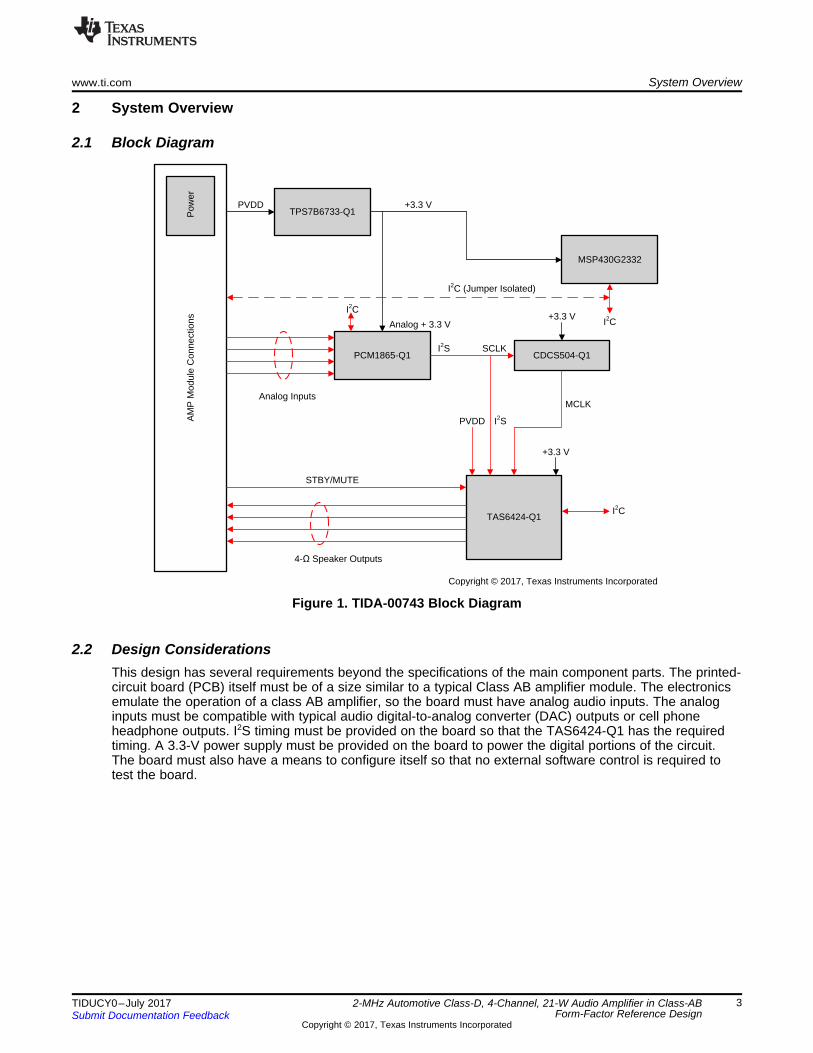
2.1 Block Diagram
Figure 1. TIDA-00743 Block Diagram
2.2 Design ConsiderationsThis design has several requirements beyond the specifications of the main component parts. The printed-circuit board (PCB) itself must be of a size similar to a typical Class AB amplifier module. The electronicsemulate the operation of a class AB amplifier, so the board must have analog audio inputs. The analoginputs must be compatible with typical audio digital-to-analog converter (DAC) outputs or cell phoneheadphone outputs. I2S timing must be provided on the board so that the TAS6424-Q1 has the requiredtiming. A 3.3-V power supply must be provided on the board to power the digital portions of the circuit.The board must also have a means to configure itself so that no external software control is required totest the board.
VDD VCOM VBAT GVDD PVDD
OUT_1P
OUT_1M
OUT_2P
OUT_2M
OUT_3P
OUT_3M
OUT_4P
OUT_4M
VREG
I2C_ADDR1
I2C_ADDR0
SDA
SCL
I2C Control
SDIN1
SDIN2
SCLK
FSYNC
MCLK
Serial
Audio
Port
PLL and Clock
Management
STANDBY
WARN
FAULT
Digital Core
Reference
Regulators
Gate Drive
Regulator
Channel 1
Powerstage
Channel 2
Powerstage
Channel 3
Powerstage
Channel 4
Powerstage
Volume Control
-100 to +24 dB
0.5 dB steps
Gate
Drives
Digital to PWM
Clip
Detection
Closed Loop Class D Amplifier
Overcurrent Limit
Protection
Overcurrent
Overtemperature
Overvoltage and Undervoltage
DC Detection
Short to GND
DC Load Diagnostics
Short to Power
Open Load
Shorted Load
AC Load Diagnostics
MUTE
Copyright © 2016, Texas Instruments Incorporated
System Overview www.ti.com
4 TIDUCY0–July 2017Submit Documentation Feedback
Copyright © 2017, Texas Instruments Incorporated
2-MHz Automotive Class-D, 4-Channel, 21-W Audio Amplifier in Class-ABForm-Factor Reference Design
2.3 Highlighted Products
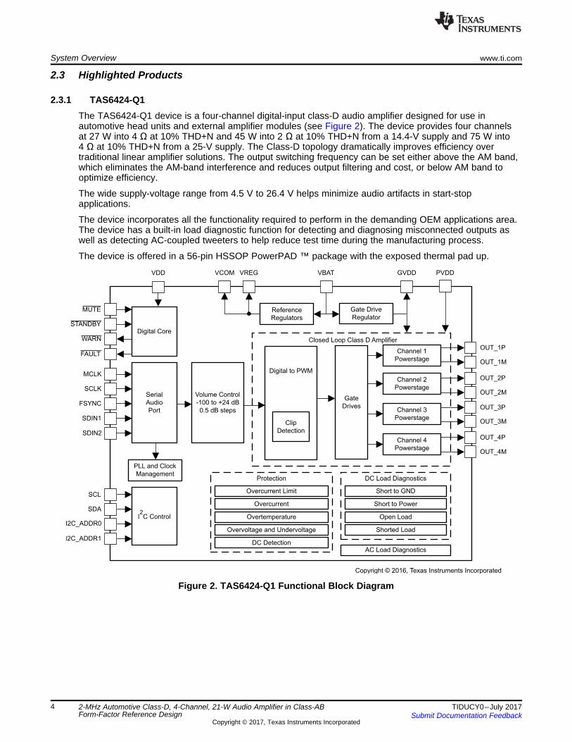
2.3.1 TAS6424-Q1The TAS6424-Q1 device is a four-channel digital-input class-D audio amplifier designed for use inautomotive head units and external amplifier modules (see Figure 2). The device provides four channelsat 27 W into 4 Ω at 10% THD+N and 45 W into 2 Ω at 10% THD+N from a 14.4-V supply and 75 W into4 Ω at 10% THD+N from a 25-V supply. The Class-D topology dramatically improves efficiency overtraditional linear amplifier solutions. The output switching frequency can be set either above the AM band,which eliminates the AM-band interference and reduces output filtering and cost, or below AM band tooptimize efficiency.
The wide supply-voltage range from 4.5 V to 26.4 V helps minimize audio artifacts in start-stopapplications.
The device incorporates all the functionality required to perform in the demanding OEM applications area.The device has a built-in load diagnostic function for detecting and diagnosing misconnected outputs aswell as detecting AC-coupled tweeters to help reduce test time during the manufacturing process.
The device is offered in a 56-pin HSSOP PowerPAD ™ package with the exposed thermal pad up.
Figure 2. TAS6424-Q1 Functional Block Diagram

180
RESET
NC
DELAY
VOUT
ADJ/NC
NC
NC
GND
NC
VIN
NC
NC
NC
EN
NC
GND
1
2
3
4
5
6
7
8
14
15
16
17
18
19
20
NC
NC
NC
NC
9 12
10
13
11 Large Pad on EVMEnhances ThermalDissipating
www.ti.com System Overview
5TIDUCY0–July 2017Submit Documentation Feedback
Copyright © 2017, Texas Instruments Incorporated
2-MHz Automotive Class-D, 4-Channel, 21-W Audio Amplifier in Class-ABForm-Factor Reference Design
2.3.2 TPS7B6733-Q1The TPS7B6701-Q1, TPS7B6733-Q1, and TPS7B6750-Q1 devices (TPS7B67xx-Q1) are low-dropoutlinear regulators designed for up to 40-V VIN operations (see Figure 3). These devices drive loads up to450 mA with only 15-µA quiescent current at light load, which greatly increases the endurance time of theautomotive battery.
The TPS7B67xx-Q1 family of devices features an integrated short-circuit and overcurrent protection.Reset delay and power-good signal are implemented on power-up to indicate that the output voltage isstable and is in regulation. An external capacitor programs the delay. The enable function activates anddeactivates the device with an I/O port from the MCU.
The device family operates at a temperature range of –40°C to 125°C.
Figure 3. TPS7B6733-Q1 Enhanced Thermal Pad
2.3.3 PCM1865-Q1The PCM1865-Q1 audio front-end device takes a new approach to audio-function integration to easecompliance with European Ecodesign legislation while enabling high-performance end products (seeFigure 4). Smaller, smarter products are becoming increasingly feasible at reduced costs without therequirement for a 5-V supply or an external programmable-gain amplifier.
The highly-flexible audio front end of the PCM1865-Q1 supports input levels from small-mV microphoneinputs to 2.1-VRMS line inputs without external resistor dividers. The PCM1865-Q1 integrates many system-level functions that assist or replace some digital signal processing (DPS) functions.
All of these features are available using a single 3.3-V power supply. An integrated band-gap voltagereference provides excellent power supply rejection ratio (PSRR) such that a dedicated analog 3.3-V railmay not be required.

GND
OUTIN
FS
LVCMOS
ControlLogic
OE
LVCMOS
GND
GND
x1 or x4
VDD
Copyright © 2017, Texas Instruments Incorporated
Mix,
Mux
PrimaryADC
(CH2L)
Secondary
ADC
PrimaryADC
(CH1R)
VINL 4 (4M)
VINL3 (4P)
VINL2 (1M)
VINL1 (1P)
Mix,
Mux
VINR1 (2P)
VINR2 (2M)
VINR4 (3M)
VINR3 (3P)
MD0/Mode
MD1/ADR1/MS
MD2/SDA/MOSI
MD3/SCL/SBCK
MD4/MISO/GPIO0
MD5/(INT A/ DMIM/GPIO1)
MD6/(DM CLK/GPIO2)
INT/(INT C/GPIO3)
Control ,
GPIO,
Interrupt and
Digital Mic
Interface
DOUT
Clocks, PLLPower
LD
O
DG
ND
DV
DD
IOV
DD
AG
ND
AV
DD XI
XO
SC
K
BC
K
LR
CK
PCM1865-Q1
ReferenceVREF
Mic Bias
AudioSerial
Port
(LJ, I2S,
TDM)
PrimaryADC
(CH1L)
PrimaryADC
(CH2R)
DOUT 2
DM
IC/
DIN
Co
ntr
ol,
GP
IO,In
terr
up
t,
Dig
italM
icIn
terf
ace
Mix
erand
Ener
gys
ens
e
DS
Ps
Copyright © 2017, Texas Instruments Incorporated
System Overview www.ti.com
6 TIDUCY0–July 2017Submit Documentation Feedback
Copyright © 2017, Texas Instruments Incorporated
2-MHz Automotive Class-D, 4-Channel, 21-W Audio Amplifier in Class-ABForm-Factor Reference Design
Figure 4. PCM1865-Q1 Simplified Block Diagram
2.3.4 CDCS504-Q1The CDCS504-Q1 device is a LVCMOS input clock buffer with selectable frequency multiplication (seeFigure 5).
The CDCS504-Q1 has an output enable pin. The device accepts a 3.3-V LVCMOS signal at the input. Theinput signal is processed by a phased-locked loop (PLL), whose output frequency is either equal to theinput frequency or multiplied by the factor of four. By this, the device can generate output frequenciesbetween 2 MHz and 108 MHz. A separate control pin can be used to enable or disable the output. TheCDCS504-Q1 device operates in a 3.3-V environment.
The device is characterized for operation from –40°C to 105°C and is available in an eight-pin TSSOPpackage.
Figure 5. CDCS504-Q1 Functional Block Diagram
Clock
System
Brownout
Protection
RST/NMI
DVCC DVSS
MCLK
Watchdog
WDT+
15-Bit
Timer0_A3
3 CC
Registers
16MHz
CPU
incl. 16
Registers
Emulation
2BP
JTAG
Interface
SMCLK
ACLK
MDB
MAB
Port P1
8 I/O
Interrupt
capability
pullup/down
resistors
P1.x
8
Spy-Bi
Wire
XIN XOUT
RAM
256B
256B
256B
128B
Flash
8KB
4KB
2KB
1KB
P2.x
Port P2
up to 8 I/O
Interrupt
capability
pullup/down
resistors
up to 8
USI
Universal
Serial
Interface
SPI, I2C
ADC
10-Bit
8 Ch.
Autoscan
1 ch DMA
www.ti.com System Overview
7TIDUCY0–July 2017Submit Documentation Feedback
Copyright © 2017, Texas Instruments Incorporated
2-MHz Automotive Class-D, 4-Channel, 21-W Audio Amplifier in Class-ABForm-Factor Reference Design
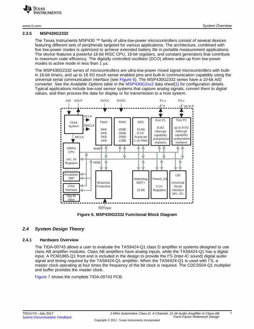
2.3.5 MSP430G2332The Texas Instruments MSP430 ™ family of ultra-low-power microcontrollers consist of several devicesfeaturing different sets of peripherals targeted for various applications. The architecture, combined withfive low-power modes is optimized to achieve extended battery life in portable measurement applications.The device features a powerful 16-bit RISC CPU, 16-bit registers, and constant generators that contributeto maximum code efficiency. The digitally controlled oscillator (DCO) allows wake-up from low-powermodes to active mode in less than 1 μs.
The MSP430G2332 series of microcontrollers are ultra-low-power mixed signal microcontrollers with built-in 16-bit timers, and up to 16 I/O touch sense enabled pins and built-in communication capability using theuniversal serial communication interface (see Figure 6). The MSP430G2332 series have a 10-bit A/Dconverter. See the Available Options table in the MSP430G2xx2 data sheet[1] for configuration details.Typical applications include low-cost sensor systems that capture analog signals, convert them to digitalvalues, and then process the data for display or for transmission to a host system.
Figure 6. MSP430G2332 Functional Block Diagram
2.4 System Design Theory
2.4.1 Hardware OverviewThe TIDA-00743 allows a user to evaluate the TAS6424-Q1 class D amplifier in systems designed to useclass AB amplifier modules. Class AB amplifiers have analog inputs, while the TAS6424-Q1 has a digitalinput. A PCM1865-Q1 front end is included in the design to provide the I2S (Inter-IC sound) digital audiosignal and timing required by the TAS6424-Q1 amplifier. When the TAS6424-Q1 is used with I2S, amaster clock operating at four times the frequency of the bit clock is required. The CDCS504-Q1 multiplierand buffer provides the master clock.
Figure 7 shows the complete TIDA-00743 PCB.

System Overview www.ti.com
8 TIDUCY0–July 2017Submit Documentation Feedback
Copyright © 2017, Texas Instruments Incorporated
2-MHz Automotive Class-D, 4-Channel, 21-W Audio Amplifier in Class-ABForm-Factor Reference Design
Figure 7. TIDA-00743 PCB

RESET1
NC2
DELAY3
VOUT4
NC5
NC6
NC7
GND8
NC9
NC10
NC11
NC12
GND13
NC14
EN15
NC16
NC17
NC18
VIN19
NC20
PAD21
U5
TPS7B6733QPWPRQ1
GNDGND
+3P3V
PVDD
10µF
50V
C1
2200pF
50V
C66
10µF
10V
C67
0
R40
0.1µF
50V
C71
GND
3V3_OUT
Copyright © 2017, Texas Instruments Incorporated
www.ti.com System Overview
9TIDUCY0–July 2017Submit Documentation Feedback
Copyright © 2017, Texas Instruments Incorporated
2-MHz Automotive Class-D, 4-Channel, 21-W Audio Amplifier in Class-ABForm-Factor Reference Design
2.4.1.1 PCB Outline and InterfaceThe PCB is designed to resemble a typical class AB audio power amplifier that stands vertically from amain system PCB and mounts to a heat sink. The board outline and mounting hole positions have notbeen copied from a specific amplifier module. The main connector is a standard two-row header connectorwith 2.54-mm (100-mil) pin spacing. The board size is 53.5 mm by 42.3 mm (2.11 in by 1.665 in).
2.4.1.2 PowerThe power supplied to the TIDA-00743 design can be in the range of a typical automotive battery. TheTAS6424-Q1 has two power rails which connect directly to a main power input. VBAT is connected to theTAS6424-Q1 at pin 3. VBAT can be in the range of 4.5 V to 18 V. PVDD must be in the range of 4.5 V to26.4 V. The module input voltage must be limited to less that 18 V because VBAT is the limiting voltage.The rest of the components in the system operate at 3.3 V, so a regulator is provided to create 3.3 V fromthe input voltage.
2.4.1.2.1 TPS7B6733-Q1The TPS7B6733-Q1 linear regulator provides the regulated 3.3-VDC required by the other active parts inthe subsystem. The TPS7B6733-Q1 has been selected because its input voltage range is 4 V to 40 V.The TPS7B6733 package is designed to dissipate heat through a thermal pad and extra pins on thedevice, which enable it to source as much as 450 mA (see Figure 8). The 450-mV dropout voltage of theTPS7B6733-Q1 allows it to maintain output regulation when the input voltage drops to the 4.5-V minimumvoltage for the TAS6424-Q1.
Figure 8. TPS7B6733-Q1 Linear Regulator Circuit
2.4.1.3 PCM1865-Q1The PCM1865-Q1 is ideal for this design (see Figure 9). Four ADC channels are required to provide thefour channels of digital data for the TAS6424-Q1. The PCM1865-Q1 (U4) has an internal clock generatorto create either I2S or time-division multiplexed (TDM) data streams. A 24.576-MHz crystal, Y1, acts as thetiming reference for the PCM1865-Q1 device.
The power to the PCM1865-Q1 is +3.3 V. The digital IO and internal digital circuits are supplied throughIOVDD and DVDD, which are connected together. R24 is included to allow measurement of digital currentand in case extra filtering is desired. C46 acts as a bypass capacitor and is placed close to U4 pins 13and 14. The +3.3 V for the analog section, AVDD, is filtered by L25, C47 and C48. C48 is placed close toU4 pin 8 to provide a bypass to ground.

2.2µF
6.3V
C49
SCLK
LRCLK
DOUT
VINL1/VIN1P3
VINR1/VIN2P4
VINL2/VIN1M1
VINR2/VIN2M2
VINL3/VIN4P29
VINR3/VIN3P30
VINL4/VIN4M27
VINR4/VIN3M28
AVDD8
DVDD13
IOVDD14
AGND7
DGND12
LDO11
VREF6
MICBIAS5
XO9
XI10
SCKI15
BCK17
LRCK16
DOUT18
MD026
MS/AD25
MC/SCL24
MOSI/SDA23
MISO/GPIO0/DMIN222
GPIO2/INTB/DMCLK20
GPIO1/INTA/DMIN21
GPIO3/INTC19
U4
PCM1865QDBTRQ1
0.1µF
50V
C46
+3P3V
0.1µF
50V
C48
GND
10µF
10V
C44
GND
0
R24 3V3_1865A1
1000 ohm
L253V3_1865D1
+3P3V
0.1µF
50V
C502.2µF
6.3V
C51
10µF10V
C52
10µF10V
C55
10µF10V
C56
10µF10V
C57
GND
SCL
SDA
100kR39
100kR38
100kR37
100kR36
GND
Rear_L
0
R28
0
R30
0
R32
0
R34
I2S_ADSEL_1865_1
10.0kR26
DNP
10.0kR27
GND
+3P3V
1
3 4
2GG
24.576Mhz
Y1
20pF
50V
C5320pF
50V
C54
GND
GND
DOUT2
145 mW at 3.3V - 45 ma
Low for adress 0x94High for address 0x96
0.1µF
50V
C580.1µF
50V
C61
GND
1P8V
XIXO
TP8
TP9
TP10 TP11
0.01µFC64
0.01µFC62
0.01µFC65
0.01µFC63
100
R29
100
R31
100
R33
100
R35
GND
Front_L
Rear_R
Front_RFR_R_ATTN
FR_L_ATTN
REAR_R_ATTN
0R10
DNP
2L
1L
2R
1R
GND
0.1µF
50V
C600.1µF
50V
C59
0
R9DNP
0
R14DNP
10µF
10V
C47
REAR_L_ATTN
Copyright © 2017, Texas Instruments Incorporated
System Overview www.ti.com
10 TIDUCY0–July 2017Submit Documentation Feedback
Copyright © 2017, Texas Instruments Incorporated
2-MHz Automotive Class-D, 4-Channel, 21-W Audio Amplifier in Class-ABForm-Factor Reference Design
The four analog inputs to the PCM1865-Q1 are configured as single-ended inputs. Several passivecomponents are required to couple the analog signal into each ADC channel of the PCM1865 device.Input channel VIN1L is fed from the signal Front_L. R28 and R36 form a resistive divider for use withsignals that are greater than 2.1 VRMS. R28 is populated with a 0-Ω resistor while R36 has a 100-kΩresistor to act as the signal load. If a signal source has an amplitude higher than 2.1 VRMS, R28 and R36can be changed to provide some attenuation to the signal before it reaches the PCM1865-Q1 device.Capacitor C52 AC-couples the input signal to prevent a DC bias from saturating or otherwise damagingthe input. R29 and C64, which are 100 Ω and 0.01 µF, respectively, form a low-pass filter with a cutofffrequency of 159 kHz. The high cutoff frequency is chosen to ensure that the signal has only beenattenuated by –0.077 dB at 20 kHz. All four analog inputs have the same circuit. Several unpopulatedresistors can also be used to jumper the different inputs together so that one signal source can drivemultiple channels. The four input channels have a corresponding output channel on the TAS6424-Q1:• Input Front_L drives output channel 1• Input Front_R drives output channel 2• Input Rear_L drives output channel 3• Input Rear_R drives output channel 4
The digital interface on the PCM1865-Q1 includes an I2C interface and the digital audio interface. The I2Cinterface connects to the system MCU and is used to configure the PCM1865-Q1. The digital audiointerface consists of four signals: SCLK, LRCLK, DOUT, and DOUT2. SCLK is the serial or BIT clock. Insome applications and on the PCM1865-Q1 data sheet, this signal is called BCLK or BCK. The LRCLKsignal is the left-right clock, also known as the word clock. This clock indicates whether the current dataword is the left or right channel data. The frequency of LRCLK is equal to the sampling clock frequency.DOUT and DOUT2 are the data outputs. I2S data has two data words per output, so DOUT2 is configuredby software to create a data lane for the second data pair. The DOUT data words are 24 bits each, thoughthe data stream is configured for 32-bit words. For this design, the audio sampling rate is 96 kHz.Consequently, SCLK is 6.144 MHz. The audio sampling rate can be set at either 48 kHz or44.1 kHz if desired.
Figure 9. PCM1865-Q1 Circuit

IN1
GND2
GND3
GND4
FS5
OUT6
OE7
VDD8
U2
CDCS504TPWRQ1
+3P3V
GND
10.0kR150.1µF
50V
C41
GND
SCLK MCLK
FS High for 4x mult, low for TDM mode
TP1
FS
Copyright © 2017, Texas Instruments Incorporated
www.ti.com System Overview
11TIDUCY0–July 2017Submit Documentation Feedback
Copyright © 2017, Texas Instruments Incorporated
2-MHz Automotive Class-D, 4-Channel, 21-W Audio Amplifier in Class-ABForm-Factor Reference Design
2.4.1.4 CDCS504-Q1The CDCS504-Q1 is a clock buffer and clock multiplier IC (see Figure 10). In this design, the CDCS504-Q1 is used to multiply the 6.144-MHz SCLK four times in frequency to provide a 24.576-MHz masterclock, or MCLK, to the TAS642-Q1 device. If TDM operation is desired, the MSP430 MCU can set the FSsignal low so that the CDCS504-Q1 device does not multiply SCLK. The SCLK is 24.576 MHz if theTIDA-00743 module board is configured for TDM mode.
Figure 10. CDCS504-Q1 Circuit
2.4.1.5 TAS6424-Q1The TAS6424-Q1 is a 75-W class-D audio power amplifier that operates with a switching frequency of2.1 MHz (see Figure 11). The TAS6424-Q1 has a digital audio input that is compatible with I2S and TDMdigital audio data. The digital audio input enables a system designer to eliminate an analog signal chainthat connects from an audio DAC, through the circuit board, and to the power amplifier. Removing thisanalog signal chain reduces the risk of noise interference in the audio signal. The TAS6424-Q1 has loaddump protection, so the power pins for PVDD and PVDD can be connected directly to the car battery system.
The TAS6424-Q1 (U1) has three voltage inputs. VDD is a logic-level supply connected at U1 pin 19 andmust be in the range of 3 V to 3.5 V. VBAT is connected to the TAS6424-Q1 at pin 3. PVDD connects to U1pins 2, 29, 30, 42, 43, 55, and 56. Other voltages are generated inside the TAS6424-Q1. VREG is aninternal regulator, which is bypassed to AREF by C19. VCOM is an internal reference, which C21 bypasses toAREF. The two voltages GVDD form the gate drive for the output high-side MOSFETs. U1 pin 9 is the GVDDfor outputs 3 and 4 while pin 10 is the GVDD for outputs 1 and 2. Both pins are bypassed to ground with1-µF capacitors.
Pins 12 through 16 form the digital audio input to the TAS6424-Q1 device from the PCM1865-Q1 device.Pins 20 and 21 are the I2C interface. Pins 22 and 23 set the address for the I2C. In this design, Pin 23 isalways grounded because there are no other TAS6424 devices in the system. Pin 24 is the nSTANDBYfunction. If this signal is set low, the TAS6424-Q1 device is in a low-power standby state. This function isnot used in TIDA-00743. Pin 25 is the nMUTE function. When this signal is low, the outputs of theTAS6424-Q1 are muted, but the operating state of the device is maintained. Pins 24 and 25 must bepulled up by resistors or a processor for the TAS6424-Q1 device to operate. Pins 26 and 27 are open-drain outputs. These pins can be used as light-emitting diode (LED) drivers, as shown in Figure 11, or asprocessor interrupts. Pin 26 is asserted low when a defined fault condition exists. Pin 27 is asserted lowwhen clipping occurs or if the TAS6424-Q1 has passed the overtemperature warning threshold. See theTAS6424-Q1 data sheet[2] for more details.

AVDD8
BST_1M31
BST_1P35
BST_2M37
BST_2P41
BST_3M44
BST_3P48
BST_4M50
BST_4P54
FSYNC14
GND33
GND7
GND36
GND39
GND11
GND1
GND46
GND18
GND49
GND28
GND52
AREF4
GVDD10
GVDD9
I2C_ADDR022
I2C_ADDR123
MCLK12
OUT_1M32
OUT_1P34
OUT_2M38
OUT_2P40
OUT_3M45
OUT_3P47
OUT_4M51
OUT_4P53
PVDD30
PVDD2
PVDD42
PVDD43
PVDD29
PVDD55
PVDD56
GND17
SCL20
SCLK13
SDA21
SDIN115
SDIN216
VBAT3
VCOM6
VDD19
VREG5
FAULT26
MUTE25
STANDBY24
WARN27
U1
TAS6424QDKQRQ1
FDSD0420-H-3R3M
3.3µH
L1
FDSD0420-H-3R3M
3.3µH
L2
FDSD0420-H-3R3M
3.3µH
L3
FDSD0420-H-3R3M
3.3µH
L4
FDSD0420-H-3R3M
3.3µH
L5
FDSD0420-H-3R3M
3.3µH
L6
FDSD0420-H-3R3M3.3µH
L7
FDSD0420-H-3R3M
3.3µH
L8
1µF
50V
C17
1µF
50V
C25
1µF
50V
C31
1µF
50V
C39
0.01µF
50V
C11
1µF25V
C14
GND
GND
GND
GND
GND
GND
GND
GND
GND
GND
OUT1M
OUT1P
OUT2M
OUT2P
OUT3M
OUT3P
OUT4M
OUT4P
OUT1+
OUT3-
OUT3+
OUT2+
OUT2-
OUT4+
OUT4-
OUT1-
0.1µF
50V
C3
1µF25V
C16
1µF25V
C20
1µF25V
C23
1µF25V
C27
1µF25V
C30
1µF25V
C33
1µF25V
C34
1µF
50V
C35
1µF
50V
C37
1µF
50V
C12
1µF
50V
C10
0.01µF
50V
C13
0.01µF
50V
C18
0.01µF
50V
C26
0.01µF
50V
C32
0.01µF
50V
C36
0.01µF
50V
C38
0.01µF
50V
C40
10µF
50V
C2
PVDD
0.1µF
50V
C22
GND
PVDD
0
R1 U1_VBAT
100k
R5DNP
10.0kR7
1µF
25V
C21
1µF25V
C24
1µF25V
C281µF25V
C29
1µF25V
C19AREF
0R3
GND
AVDD_GND
AVDD_GND
OUT4+
OUT4-
OUT3+
OUT3-
OUT2+
OUT2-
OUT1+
OUT1-
10.0kR8
+3P3V
nSTANDBY
nMUTE
4.99k
R6
GND
+3P3V
I2C_A0
SCL
SDA
MCLK
SCLK
LRCLK
DOUT
+3P3V
1µF25V
C15
GND
GND
0.1µF
50V
C510µF
50V
C4
PVDD
GND
0.1µF
50V
C710µF
50V
C6
PVDD
GND
0.1µF
50V
C910µF
50V
C8
PVDD
DOUT2
I2C Address
Bit State I2C Address(A1/A0)
00 0xD4/0xD501 0xD6/0xD710 0xD8/0xD911 0xDA/0xDB
nSTANDBY
nMUTE
150060YS75000Yellow
2 1
D2
150060SS75000Super Red
2 1
D1
1.00k
R12
1.00k
R13
+3P3V
nWARN1
nFAULT1
10uF caps are taller than TAS6424
nWARN1
Place on side of board opposite TAS6424
Copyright © 2017, Texas Instruments Incorporated
System Overview www.ti.com
12 TIDUCY0–July 2017Submit Documentation Feedback
Copyright © 2017, Texas Instruments Incorporated
2-MHz Automotive Class-D, 4-Channel, 21-W Audio Amplifier in Class-ABForm-Factor Reference Design
Each output channel is a bridge-tied load (BTL) output. This topology requires a low-pass filter for both thepositive- and negative-going outputs of each channel. The output inductors for TIDA-00743 have beenchosen to be shorter than a TAS6424-Q1 device so that the heat sink does not create any mechanicalinterference form the inductors. The size of the inductors also limits the output impedance to be 4 Ω orhigher. The design of the filter follows the reference schematic on the TAS6424-Q1 data sheet. Thechoice of inductor has a great impact on the THD of the amplifier circuit and also determines whether alower impedance load is possible. Typically, smaller inductors yield a higher THD while larger inductorsyield a lower THD and greater current capacity. The inductors chosen for this design are a balancebetween size and performance.
Figure 11. TAS6424-Q1 Class-D Power Audio Amplifier Circuit

DVCC1
P2.210
P2.311
P2.412
P2.513
P1.6/TA0.1/SDO/SCL/A6/TDI/TCLK14
P1.0/TA0CLK/ACLK/A02
P1.1/TA0.0/A13
P1.2/TA0.1/A24
P1.3/ADC10CLK/VREF-/VEREF-/A35
P1.4/TA0.2/SMCLK/A4/VREF+/VEREF+/TCK6
P1.5/TA0.0/SCLK/A5/TMS7
P2.08
P2.19
P1.7/SDI/SDA/A7/TDO/TDI15
RST/NMI/SBWTDIO16
TEST/SBWTCK17
XOUT/P2.718
XIN/TA0.1/P2.619
DVSS20
U3
MSP430G2332QPW2REP
+3P3V
SCL
SDA
0.1µF
50V
C42
1
2
3
4
5
6
J4
851-43-006-20-001000
GND
0R18
DNP
nRST_TDIOSBWTCK
GND
GND
SCLSDA
nWARN1
nFAULT1
+3P3V
47.5kR21
2200pF
50V
C43
+3P3V
GNDGND
DNP
FS
VOL_UPVOL_DN
21
S1
nFAULT1nWARN1
nSTANDBY
Copyright © 2017, Texas Instruments Incorporated
www.ti.com System Overview
13TIDUCY0–July 2017Submit Documentation Feedback
Copyright © 2017, Texas Instruments Incorporated
2-MHz Automotive Class-D, 4-Channel, 21-W Audio Amplifier in Class-ABForm-Factor Reference Design
2.4.1.6 Support Circuits
2.4.1.6.1 MSP430G2332-EPCreating a stand-alone design requires a host processor to configure the PCM1865-Q1 and the TAS6424-Q1 at power up. The MSP430G2332-EP has been chosen because this board design is intended for anextended temperature range. The I2C interface that connects to the PCM1865-Q1 and the TAS6424-Q1 isthe primary interface from the MSP430 to the other components on the board (see Figure 12). J4 is theprogramming interface for the MSP430. R21 and C43 provide a delayed power-up reset function. SwitchS1 allows a user to reset the MSP430 without cycling power to the board. The signal FS controls themultiply function on the CDCS504-Q1 as described in Section 2.4.1.4. The signals nWARN1 andnFAULT1 are routed from theTAS6424-Q1 to the MSP430, but there is no provision in the software to actupon faults or warnings.
Figure 12. TIDA-00743 Microcontroller

OUT4+
OUT3+
OUT4+
OUT3+
SDA_EXTnFAULT1nWARN1
OUT3-OUT3-
OUT4-OUT4-
nMUTE
OUT2-
OUT2+OUT2+OUT2-
OUT1-OUT1-
OUT1+OUT1+
PVDD
1 2
3 4
5 6
7 8
9 10
11 12
13 14
15
17
19
21
23
25
27
29
31
16
18
20
22
24
26
28
30
32
33 34
J6
PRPC017DBAN-M71RC
nSTANDBYnSTANDBY
OUT4+
OUT3+OUT3-
OUT4-
OUT2+OUT2-
OUT1-OUT1+
SCL_EXT
Front_R
Front_L Rear_L
Rear_R
GND
Copyright © 2017, Texas Instruments Incorporated
System Overview www.ti.com
14 TIDUCY0–July 2017Submit Documentation Feedback
Copyright © 2017, Texas Instruments Incorporated
2-MHz Automotive Class-D, 4-Channel, 21-W Audio Amplifier in Class-ABForm-Factor Reference Design
2.4.1.6.2 Interface ConnectorThe interface connector J6 is a standard, two-row 100-mil (2.54-mm) spacing connector (see Figure 13).This type has been selected so that the TIDA-00743 circuit board has an interface that is similar to thetypical package for a vertically-mounted class AB amplifier IC. The inputs are arranged so that they areisolated from the power and speaker outputs by ground pins. The speaker output pins are doubled toreduce the impedance of the output connections. the signals nSTANDBY and nMUTE are brought out toallow control of those functions on the TAS6424-Q1. The I2C interface can be connected to J6 by placing0-Ω resistors in the positions for R20 and R22. This connection allows the PCM1865-Q1 and theTAS6424-Q1 to be controlled by a host processor that is not on the module circuit board. SignalsnWARN1 and nFAULT1 are the warning and fault connections from the TAS6424-Q1.
Figure 13. TIDA-00743 Interface Connector
TPS7B6733-Q1
PCM1865-Q1
MSP430G2332
CDCS504-Q1
TAS6424-Q1
PVDD +3.3 V
+3.3 V
MCLK
I2S
I2S
PVDD
I2C+3.3 VI2C
Analog Inputs
STBY/MUTE
I2C
Analog + 3.3 V
I2C (Jumper Isolated)
4- Speaker Outputs
SCLK
Pow
erA
MP
Mod
ule
Con
nect
ions
Spe
aker
O
utpu
tsA
udio
Inpu
tA
udio
Inpu
t
EMI Filter
Pow
er
Carrier BoardModule Board
Copyright © 2017, Texas Instruments Incorporated
www.ti.com System Overview
15TIDUCY0–July 2017Submit Documentation Feedback
Copyright © 2017, Texas Instruments Incorporated
2-MHz Automotive Class-D, 4-Channel, 21-W Audio Amplifier in Class-ABForm-Factor Reference Design
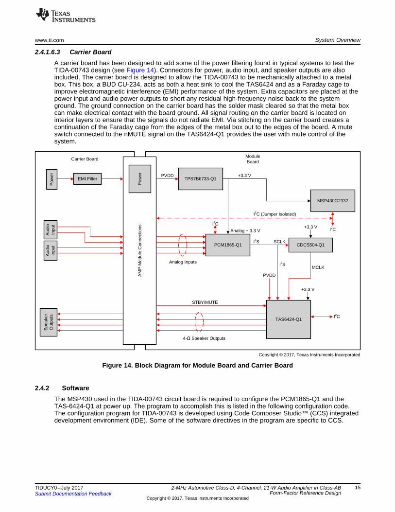
2.4.1.6.3 Carrier BoardA carrier board has been designed to add some of the power filtering found in typical systems to test theTIDA-00743 design (see Figure 14). Connectors for power, audio input, and speaker outputs are alsoincluded. The carrier board is designed to allow the TIDA-00743 to be mechanically attached to a metalbox. This box, a BUD CU-234, acts as both a heat sink to cool the TAS6424 and as a Faraday cage toimprove electromagnetic interference (EMI) performance of the system. Extra capacitors are placed at thepower input and audio power outputs to short any residual high-frequency noise back to the systemground. The ground connection on the carrier board has the solder mask cleared so that the metal boxcan make electrical contact with the board ground. All signal routing on the carrier board is located oninterior layers to ensure that the signals do not radiate EMI. Via stitching on the carrier board creates acontinuation of the Faraday cage from the edges of the metal box out to the edges of the board. A muteswitch connected to the nMUTE signal on the TAS6424-Q1 provides the user with mute control of thesystem.
Figure 14. Block Diagram for Module Board and Carrier Board
2.4.2 SoftwareThe MSP430 used in the TIDA-00743 circuit board is required to configure the PCM1865-Q1 and theTAS-6424-Q1 at power up. The program to accomplish this is listed in the following configuration code.The configuration program for TIDA-00743 is developed using Code Composer Studio™ (CCS) integrateddevelopment environment (IDE). Some of the software directives in the program are specific to CCS.

System Overview www.ti.com
16 TIDUCY0–July 2017Submit Documentation Feedback
Copyright © 2017, Texas Instruments Incorporated
2-MHz Automotive Class-D, 4-Channel, 21-W Audio Amplifier in Class-ABForm-Factor Reference Design
TIDA-00743 configuration code:#include <msp430.h>#include "USI_I2C.h"
//NOTE: Address needs to be in 7 bit form to be used with the current write and read functions.
unsigned char SLV_Test_Addr = 0x48;unsigned char PCM1_Addr = 0x4a; //PCM1865 Addressunsigned char TAS1_Addr = 0x6a; //TAS6424 Address
int main(void)
volatile unsigned int i; // Use volatile to prevent removal
WDTCTL = WDTPW + WDTHOLD; // Stop watchdogif (CALBC1_1MHZ==0xFF) // If calibration constant erased
while(1); // do not load, trap CPU!!DCOCTL = 0; // Select lowest DCOx and MODx settingsBCSCTL1 = CALBC1_1MHZ; // Set DCODCOCTL = CALDCO_1MHZ;
P1OUT = 0xC0; // P1.6 & P1.7 Pullups, others to 0P1REN |= 0xC0; // P1.6 & P1.7 PullupsP1DIR = 0xFF; // Unused pins as outputsP2OUT = 0x0C; //Set P2.2 and P2.3 High: SCLK x4, TAS operatingP2DIR = 0xFC; //P2.0 and 2.1 inputs
__delay_cycles(10000);
Set_I2C();
__delay_cycles(10000);
//PCM1865 sectionI2C_Write (I2C_BYTE, PCM1_Addr, 0x26, 0x03); //Set BCLK Divider from SCK to 1/4 on PCM1865 -
96 kHz for LR CLKI2C_Write (I2C_BYTE, PCM1_Addr, 0x10, 0x51); // Set GPIO1 as DOUT2 on PCM1865I2C_Write (I2C_BYTE, PCM1_Addr, 0x20, 0x91); // Set as timing master on PCM1865
//TAS6424 sectionI2C_Write (I2C_BYTE, TAS1_Addr, 0x04, 0x55); // Mute outputs on TAS6424I2C_Write (I2C_BYTE, TAS1_Addr, 0x00, 0x80); //Master Reset TAS6424.I2C_Write (I2C_BYTE, TAS1_Addr, 0x21, 0x80); //Clear Clock Fault
I2C_Write (I2C_BYTE, TAS1_Addr, 0x01, 0x31); // Set Gain to Level 2 (15V) on TAS6424 1
I2C_Write (I2C_BYTE, TAS1_Addr, 0x02, 0x62); // Set PWM for 44x FS on TAS6424I2C_Write (I2C_BYTE, TAS1_Addr, 0x03, 0x84); // Set Sampling Rate to 96 kHz on TAS6424__delay_cycles(100000);I2C_Write (I2C_BYTE, TAS1_Addr, 0x05, 0x0f); // Turn down Channel 1 on TAS6424I2C_Write (I2C_BYTE, TAS1_Addr, 0x06, 0x0f); // Turn down Channel 2 on TAS6424I2C_Write (I2C_BYTE, TAS1_Addr, 0x07, 0x0f); // Turn down Channel 3 on TAS6424I2C_Write (I2C_BYTE, TAS1_Addr, 0x08, 0x0f); // Turn down Channel 4 on TAS6424__delay_cycles(1000000); // Anti-pop delayI2C_Write (I2C_BYTE, TAS1_Addr, 0x04, 0x00); // Un-mute outputs on TAS6424I2C_Write (I2C_BYTE, TAS1_Addr, 0x05, 0xd1); // Turn Up Channel 1 on TAS6424I2C_Write (I2C_BYTE, TAS1_Addr, 0x06, 0xd1); // Turn Up Channel 2 on TAS6424I2C_Write (I2C_BYTE, TAS1_Addr, 0x07, 0xd1); // Turn Up Channel 3 on TAS6424I2C_Write (I2C_BYTE, TAS1_Addr, 0x08, 0xd1); // Turn Up Channel 4 on TAS6424
LPM0;

www.ti.com System Overview
17TIDUCY0–July 2017Submit Documentation Feedback
Copyright © 2017, Texas Instruments Incorporated
2-MHz Automotive Class-D, 4-Channel, 21-W Audio Amplifier in Class-ABForm-Factor Reference Design
The include file, msp430.h, is part of the MSP430Ware™ software library provided by Texas Instrumentsas an add-on to CCS. The include file USI_I2C.h defines the I2C commands used by the universal serialinterface (USI) block in the MSP430G2332. Next, two variables are declared to represent the I2Caddresses of the TAS6424-Q1 and the PCM1865-Q1.
The main function starts after the declarations. The first commands are a test to ensure that the calibrationfor the MSP430 internal clock is valid. If the clock calibration is valid, the clock and the GPIO for banks 1and 2 are set up. This step is followed by a delay to ensure that the GPIO outputs are settled. The I2Csection is then set up.
The next section contains three commands to configure the PCM1865-Q1 device. The first command is:I2C_Write (I2C_BYTE, PCM1_Addr, 0x26, 0x03);
This command sets the master clock-to-BCLK divide ratio. The command shown sets the BCLK to ¼th thevalue of the 24.576-MHz timing crystal, or 6.144 MHz. Note that BCLK, or bit clock, is the signal SCLK inthe previous schematic images.
The second command is:I2C_Write (I2C_BYTE, PCM1_Addr, 0x10, 0x51);
This command configures the PCM1865 GPIO1 as DOUT2, which is digital output 2. Two digital outputsare required because there are two audio channels per data output and four outputs are required.
The third command is:I2C_Write (I2C_BYTE, PCM1_Addr, 0x20, 0x91);
This command sets the PCM1865-Q1 as the timing master for the I2S bus. The rest of the registers areallowed to keep their default settings.
The TAS6424-Q1 configuration setting is more complicated:I2C_Write (I2C_BYTE, TAS1_Addr, 0x00, 0x80);I2C_Write (I2C_BYTE, TAS1_Addr, 0x04, 0x55);I2C_Write (I2C_BYTE, TAS1_Addr, 0x21, 0x80);I2C_Write (I2C_BYTE, TAS1_Addr, 0x01, 0x31);
The first command in the TAS6424-Q1 configuration setting is a master reset for the TAS6424-Q1. Thiscommand restarts the part. The second command ensures the outputs are muted so that nothing can beheard during configuration. The third command clears the clock fault register. At power up, a clock fault isregistered because there is no clock input to the device until the PCM1865-Q1 device has beenconfigured. After the PCM1865-Q1 device has been configured, the TAS6424-Q1 operates correctly, butthe fault register must be cleared by the host processor. The fourth command sets the TAS6424-Q1 gainto be appropriate for a 15-V PVDD power rail. This setting ensures that the output reaches its maximum at15 V. This setting is appropriate for the 14.4-V test level that is used to test the TIDA-00743. Otherfunctions are also controlled in register 0x01: high-pass filter enable, global overtemperature warningcontrol set point, overcurrent level set point, and volume rate. These other functions are maintained attheir default values.
The next two commands configure the clocking for the TAS6424-Q1:I2C_Write (I2C_BYTE, TAS1_Addr, 0x02, 0x62);
The first clock configuration command sets the pulse width modulator (PWM) frequency to 44 times fs,where frame sync fs is the frequency of the LRCLK. The Output Switch Frequency Option table of theTAS6424-Q1 data sheet[2] shows that the PWM settings for either a 48-kHz sample rate or a 96-kHzsample rate results in a PWM frequency of 2.11 MHz when bits 6 through 4 of register 0x02 are set to110, or 6h. The other functions in register 0x02 are set for their defaults.I2C_Write (I2C_BYTE, TAS1_Addr, 0x03, 0x84);__delay_cycles(100000);
The second clock configuration command sets the TAS6424-Q1 sampling rate to 96 kHz. This registeralso sets the input format to I2S, which is the default setting. There are two other settings in this registerthat are applicable only for TDM mode, which is not used in the TIDA-00743 design. The clockconfiguration is followed by a slight delay to ensure that the TAS6424-Q1 clocks are working correctlybefore enabling the output.

System Overview www.ti.com
18 TIDUCY0–July 2017Submit Documentation Feedback
Copyright © 2017, Texas Instruments Incorporated
2-MHz Automotive Class-D, 4-Channel, 21-W Audio Amplifier in Class-ABForm-Factor Reference Design
At this point, the TAS6424-Q1 is operating correctly and the volume must be turned up. The gain settinghas no effect because the four outputs are muted. Before setting the TAS6424-Q1 for a normal outputvolume, the four channel gains are set for a very low value. Each channel has its own register for settinggain, so four register writes are made to set all channels for the same gain:I2C_Write (I2C_BYTE, TAS1_Addr, 0x05, 0x0f);I2C_Write (I2C_BYTE, TAS1_Addr, 0x06, 0x0f);I2C_Write (I2C_BYTE, TAS1_Addr, 0x07, 0x0f);I2C_Write (I2C_BYTE, TAS1_Addr, 0x08, 0x0f);
__delay_cycles(1000000);I2C_Write (I2C_BYTE, TAS1_Addr, 0x04, 0x00);I2C_Write (I2C_BYTE, TAS1_Addr, 0x05, 0xd1);I2C_Write (I2C_BYTE, TAS1_Addr, 0x06, 0xd1);I2C_Write (I2C_BYTE, TAS1_Addr, 0x07, 0xd1);I2C_Write (I2C_BYTE, TAS1_Addr, 0x08, 0xd1);
The setting 0x0f corresponds to an output gain of –96 dB. A delay of one second is included to ensurethat there is no audible pop on the outputs. The outputs are then un-muted and set for a gain of 0xd1, or+1 dB. This value is chosen to drive the audio output to reach 10% THD + N when PVDD is 14.4 V.
A final command, LPM0, sets the MSP430 MCU into a low-power standby state.

www.ti.com System Setup and Test
19TIDUCY0–July 2017Submit Documentation Feedback
Copyright © 2017, Texas Instruments Incorporated
2-MHz Automotive Class-D, 4-Channel, 21-W Audio Amplifier in Class-ABForm-Factor Reference Design
3 System Setup and Test
3.1 Hardware SetupTwo electrical setups are used to test the TIDA-00743 design: one for bench testing of operation and onefor EMI testing.
WARNING
Hot surface. Contact may cause burns.Avoid touching to minimize the risk of burns.
3.1.1 Bench Test SetupThe primary test setup is used to characterize most of the operation parameters of the TIDA-00743design. The TIDA-00743 module board is soldered to the carrier board defined in Section 2.4.1.6.3. Thetemperature of the TAS6424-Q1 device increases during normal operation, so a heat sink must beprovided to ensure that the TAS6424-Q1 does not overheat before reaching full output power. Figure 15shows the TIDA-00743 module board with a heat sink. This screenshot also shows how the module boardattaches to the carrier board.
Figure 15. TIDA-00743 Module Board With Heat Sink Attached to Carrier Board

TIDA-00743Power Supply
4-/RDGV
Output Measurement
SignalInputs
Analog PrecisionSYS-2722
Copyright © 2017, Texas Instruments Incorporated
System Setup and Test www.ti.com
20 TIDUCY0–July 2017Submit Documentation Feedback
Copyright © 2017, Texas Instruments Incorporated
2-MHz Automotive Class-D, 4-Channel, 21-W Audio Amplifier in Class-ABForm-Factor Reference Design
Figure 16 shows another view of the boards and the connectors on the carrier board. From left to right arethe speaker outputs, the analog audio signal inputs, and the power input.
Figure 16. Connections for TIDA-00743 Assembly
Figure 17 is a diagram that shows how to make the electrical connections to the TIDA-00743 design. Thepower supply used must be capable of a 20-V output at 10 A. The power supply must be turned off untilall connections have been made. The 4-Ω output loads must be capable of dissipating at least twice theoutput power of the TAS6424-Q1. Several 100-W, 4-Ω non-inductive resistors are used as the loads forthis test. An Audio Precision SYS-2722 is used to supply the audio signal input and to measure poweroutput and THD +N. The SYS-2722 outputs are connected to the inputs for the channels to be tested andthe SYS-2722 inputs are connected to the load resistors to measure the power output and THD for thechannels of interest. For tests that require all four channels to be driven simultaneously, the inputs areconnected together so that all inputs receive the same signal level. A digital multimeter (DMM) is used tomeasure DC current and voltage at the power input.
Figure 17. Test Setup Block Diagram for Power Output and THD Tests

www.ti.com System Setup and Test
21TIDUCY0–July 2017Submit Documentation Feedback
Copyright © 2017, Texas Instruments Incorporated
2-MHz Automotive Class-D, 4-Channel, 21-W Audio Amplifier in Class-ABForm-Factor Reference Design
3.1.2 EMI Test SetupFor EMI performance testing, the TIDA-00743 design must be enclosed in a Faraday cage to ensure lowemissions. Figure 18 shows the TIDA-00743 and carrier board with the metal lid that forms the enclosure.The lid is part of a bud CU-234 box mentioned in section Section 2.4.1.6.3. Before connecting the boardassembly to the box, resistors R9, R10, and R14 are populated with 0-Ω resistors to short all of the inputstogether. The addition of these resistors allows driving the board with one input signal.
The carrier board is designed to attach to the bottom of the bud box in the place of the lid that comes withthe box. The two nuts and bolts shown on the edge of the box (see Figure 18) hold the module board tothe side of the box to provide a heat sink for the TAS-6424-Q1 device. The copper tape around the bottomedge of the box completes the ground seal between the carrier board and the box.
Figure 18. TIDA-00743 in Metal Box for EMI Tests
Figure 19 shows the TIDA-00743 electrical connection diagram. Power is provided by a 12-V car batteryto ensure that the emissions only originate from the unit under test (UUT) and not from noise generated bythe power supply. Power is routed through two line impedance stabilization networks (LISN) in accordancewith CISPR 25. 4-Ω resistive loads are connected to the amplifier outputs. The EMI test is performedinside a shielded chamber. The signal generator is placed outside the chamber and the 50-Ω shieldedcable for the 1-kHz sine wave test signal is routed through the wall of the chamber. The battery + terminalis connected after all other connections are made so that the system is not powered during test setup.

TIDA-00743
Copyright © 2017, Texas Instruments Incorporated
4-/RDGV
Power Supply
SignalGenerator
LISN
LISN
System Setup and Test www.ti.com
22 TIDUCY0–July 2017Submit Documentation Feedback
Copyright © 2017, Texas Instruments Incorporated
2-MHz Automotive Class-D, 4-Channel, 21-W Audio Amplifier in Class-ABForm-Factor Reference Design
Figure 19. Test Setup Block Diagram for EMI Tests
The two types of EMI tests are conducted emissions and radiated emissions. The conducted emissionstest is performed using the voltage method described in CISPR 25. For the conducted emission test, thepower wires from the LISNs to the UUT are 200-mm to 400-mm long. The load wires are kept short.Loads are placed close to the UUT. For radiated emissions tests, the loads are placed near the LISNs andthe UUT is placed 1.5 m from the loads. Figure 20 shows an entire EMI setup for measuring radiatedemissions in a test chamber. Both types of test are conducted with the UUT and its loads placed on a50-mm thick insulator, which is in turn placed on a table with a grounded conductive surface. See theCISPR 25 specification for more details.
Figure 20. Radiated Emissions Test Setup

Frequency (Hz)
Out
put L
evel
(dB
P)
6
6.5
7
7.5
8
8.5
9
9.5
10
20 100 1k 10k 20k
D002
Power Out (W)
VR
MS
0.001 0.01 0.1 1 10 500.01
0.1
1
10
D001
CH 1 % THD + NCH 2 % THD + NCH 3 % THD + NCH 4 % THD + N
www.ti.com System Setup and Test
23TIDUCY0–July 2017Submit Documentation Feedback
Copyright © 2017, Texas Instruments Incorporated
2-MHz Automotive Class-D, 4-Channel, 21-W Audio Amplifier in Class-ABForm-Factor Reference Design
3.2 Testing and Results
3.2.1 Power Output, Total Harmonic Distortion, and Noise (THD + N)The power output and THD + N were tested with the setup described in section Section 3.1.1. The inputsignal is set for 1 kHz during these tests. Figure 21 shows a plot of the THD + N versus power output inwatts. The power supply is set to ensure that the voltage delivered at the power input to the board is14.4 V when the outputs are driven to 10% THD. The outputs reach 10% THD + N at an output of 25.5 Wwhen all channels are driven. If only one channel is driven to 10% THD, the output power can reach ashigh as 26.5 W. The power output is 21 W per channel at 1% THD + N with all channels driven.
Figure 21. Power Output (W) versus THD + Noise (%)—Channels Driven Individually
Figure 22 shows a plot of the frequency response of the system. The frequency response was tested withthe output set to 1 W when the input frequency was 1 kHz. This graph shows that the response drops only0.7 dBµ at 20 Hz and only 0.2 dBµ at 20 kHz.
Figure 22. TIDA-00743 Frequency Response

System Setup and Test www.ti.com
24 TIDUCY0–July 2017Submit Documentation Feedback
Copyright © 2017, Texas Instruments Incorporated
2-MHz Automotive Class-D, 4-Channel, 21-W Audio Amplifier in Class-ABForm-Factor Reference Design
3.2.2 EMI
3.2.2.1 Conducted EmissionsThe EMI tests were run using the test setup described in paragraph Section 3.1.2. The following graphs ofthe tests show the test limits for CISPR 25 class 5. Figure 23 shows the ambient scan for the test setupwith the UUT unpowered. Figure 24 shows the results for conducted emissions.
Figure 23. CISPR 25 Conducted Emissions Ambient Scan
Figure 24. CISPR 25 Conducted Emissions
The TIDA-00743, when tested as previously described, has 10.5 dB of margin in the conducted emissionstest for both average and peak levels.

www.ti.com System Setup and Test
25TIDUCY0–July 2017Submit Documentation Feedback
Copyright © 2017, Texas Instruments Incorporated
2-MHz Automotive Class-D, 4-Channel, 21-W Audio Amplifier in Class-ABForm-Factor Reference Design
3.2.2.2 Radiated EmissionsFor the radiated emission tests, the UUT is set up as described in paragraph Section 3.1.2. Figure 20shows an example of the setup for radiated emissions testing.
A monopole antenna is used to receive the emissions in the frequency range of 150 kHz to 30 MHz. Onlyone polarization is measured for this antenna. Figure 25 shows the ambient scan of the test setup with theUUT unpowered. Figure 26 shows the test results.
Figure 25. CISPR 25 Radiated Emissions: 150 kHz to 30 MHz, Ambient
Figure 26. CISPR 25 Radiated Emissions: 150 kHz to 30 MHz
The average margin in the 150-kHz to 30-MHz range is greater than 10 dB for the whole range.

System Setup and Test www.ti.com
26 TIDUCY0–July 2017Submit Documentation Feedback
Copyright © 2017, Texas Instruments Incorporated
2-MHz Automotive Class-D, 4-Channel, 21-W Audio Amplifier in Class-ABForm-Factor Reference Design
For the frequency range of 30 MHz to 200 MHz, a biconical antenna is used to measure the emissions.Measurements are made with the antenna polarized both horizontally and vertically. Figure 27 andFigure 28 show the ambient scans with the UUT power OFF. Figure 29 shows the results with the antennahorizontally polarized and Figure 30 shows the results with the antenna vertically polarized.
Figure 27. CISPR 25 Radiated Emissions: 30 MHz to 200 MHz, Horizontal Antenna Orientation, AmbientScan
Figure 28. CISPR 25 Radiated Emissions: 30 MHz to 200 MHz, Vertical Antenna Orientation, Ambient Scan

www.ti.com System Setup and Test
27TIDUCY0–July 2017Submit Documentation Feedback
Copyright © 2017, Texas Instruments Incorporated
2-MHz Automotive Class-D, 4-Channel, 21-W Audio Amplifier in Class-ABForm-Factor Reference Design
Figure 29. CISPR 25 Radiated Emissions: 30 MHz to 200 MHz, Horizontal Antenna Orientation
The average margin for the horizontal polarization test is greater than 2.2 dB.
Figure 30. CISPR 25 Radiated Emissions: 30 to 200 MHz, Vertical Antenna Orientation
The average margin for the vertical polarization test is greater than 4.5 dB.

System Setup and Test www.ti.com
28 TIDUCY0–July 2017Submit Documentation Feedback
Copyright © 2017, Texas Instruments Incorporated
2-MHz Automotive Class-D, 4-Channel, 21-W Audio Amplifier in Class-ABForm-Factor Reference Design
Emissions in the frequency range from 200 MHz to 1000 MHz are measured with a horn antenna. Bothhorizontal and vertical polarizations of the antenna are tested. Figure 31 and Figure 32 show the ambientscan when the UUT power is OFF. Figure 33 and Figure 34 show the actual system response.
Figure 31. CISPR 25 Radiated Emissions: 200 MHz to 1 GHz, Horizontal Antenna Orientation, AmbientScan
Figure 32. CISPR 25 Radiated Emissions: 200 MHz to 1 GHz, Vertical Antenna Orientation, Ambient Scan

www.ti.com System Setup and Test
29TIDUCY0–July 2017Submit Documentation Feedback
Copyright © 2017, Texas Instruments Incorporated
2-MHz Automotive Class-D, 4-Channel, 21-W Audio Amplifier in Class-ABForm-Factor Reference Design
Figure 33. CISPR 25 Radiated Emissions: 200 MHz to 1 GHz, Horizontal Antenna Orientation
The average margin for the horizontal polarization test is greater than 10.8 dB.
Figure 34. CISPR 25 Radiated Emissions: 200 MHz to 1 GHz, Vertical Antenna Orientation
The average margin for the vertical polarization test is greater than 11.8 dB.

Design Files www.ti.com
30 TIDUCY0–July 2017Submit Documentation Feedback
Copyright © 2017, Texas Instruments Incorporated
2-MHz Automotive Class-D, 4-Channel, 21-W Audio Amplifier in Class-ABForm-Factor Reference Design
4 Design Files
4.1 SchematicsTo download the schematics, see the design files at TIDA-00743.
4.2 Bill of MaterialsTo download the bill of materials (BOM), see the design files at TIDA-00743.
4.3 PCB Layout RecommendationsThe TIDA-00743 module board has a six-layer PCB. Placement of the parts is important. Everything isspaced around U1, the TAS6424-Q1. U1 is close to the center of the board. The output section is orientedtoward the main connector to keep the output routing as short as possible while still leaving room for theoutput filter circuits. The analog portion of U4, the PCM1865-Q1, must be kept away from high-frequencysignals and high switching currents as much as possible. U4 is placed close to the audio input pins toreduce the possibility of noise coupling into the inputs. U5, the TPS7B6733-Q1 linear regulator, is placedclose to U4 to keep the power routing to U4 short. U3, the MSP430, is placed to the other side of theboard from U4. The placement of U3 is not critical in this design.
The PCB design requires careful consideration of signal routing, especially for the power connections. Theinput power net PVDD supplies approximately 8.5 A upon reaching the maximum audio power output, sothe power routing on the board must be capable of supplying that current. PVDD is routed on layers 1, 3,4, and 6 to ensure a low impedance for PVDD. At any place where PVDD is to be used by either U1 orU5, multiple vias are provided to maintain a low impedance. The extra vias are especially necessary forU1 pins 29, 30, 42, 43, 55, and 56. These pins are the source of the output current for the TAS6424-Q1.Layers 2 and 5 are ground planes. In addition to the two planes, unrouted areas on layers 1, 3, 4, and 6are filled with ground. This ground fill is intended to help with EMI shielding and to help dissipate heat fromU5. The net 3V3_OUT is routed with a wide trace from U5 to C71 and R40. From R40, net +3P3V isrouted primarily on layers 3 and 4 with a 30-mil (0.76-mm) wide trace. The routing of the audio inputsignals is kept as short as possible and kept as far apart as possible to reduce crosstalk. The signals forfront left and rear left are routed on the top layer, while front right and rear right are routed on the bottomlayer. Signals SCLK, DOUT, DOUT2, and LRCLK are routed on layer 3 to reduce the chances for EMI toradiate from the signals. MCLK is generated by U2 very close to where it connects to U1, so it is routed onthe surface layers. None of the other traces are very critical.
4.3.1 Layout PrintsTo download the layer plots, see the design files at TIDA-00743.
4.4 Altium ProjectTo download the Altium project files, see the design files at TIDA-00743.
4.5 Gerber FilesTo download the Gerber files, see the design files at TIDA-00743.
4.6 Assembly DrawingsTo download the assembly drawings, see the design files at TIDA-00743.
5 Software FilesTo download the software files, see the design files at TIDA-00743.

www.ti.com Related Documentation
31TIDUCY0–July 2017Submit Documentation Feedback
Copyright © 2017, Texas Instruments Incorporated
2-MHz Automotive Class-D, 4-Channel, 21-W Audio Amplifier in Class-ABForm-Factor Reference Design
6 Related Documentation1. Texas Instruments, MIXED SIGNAL MICROCONTROLLER, MSP430G2xx2 Data Sheet (SLAS723)2. Texas Instruments, TAS6424-Q1 75-W, 2-MHz Digital Input 4-Channel Automotive Class-D Audio
Amplifier With Load-Dump Protection and I2C Diagnostics, TAS6424-Q1 Data Sheet
6.1 TrademarksMSP430, Code Composer Studio, MSP430Ware are trademarks of Texas Instruments.All other trademarks are the property of their respective owners.
7 About the AuthorMARK KNAPP is a Systems Architect at Texas Instruments Incorporated who specializes in automotivepremium audio systems and instrument clusters. He also has an extensive background in video camerasystems and infrared imaging systems for military, automotive, and industrial applications. Mark earnedhis BSEE at the University of Michigan-Dearborn and his MSEE at the University of Texas at Dallas.
IMPORTANT NOTICE FOR TI DESIGN INFORMATION AND RESOURCES
Texas Instruments Incorporated (‘TI”) technical, application or other design advice, services or information, including, but not limited to,reference designs and materials relating to evaluation modules, (collectively, “TI Resources”) are intended to assist designers who aredeveloping applications that incorporate TI products; by downloading, accessing or using any particular TI Resource in any way, you(individually or, if you are acting on behalf of a company, your company) agree to use it solely for this purpose and subject to the terms ofthis Notice.TI’s provision of TI Resources does not expand or otherwise alter TI’s applicable published warranties or warranty disclaimers for TIproducts, and no additional obligations or liabilities arise from TI providing such TI Resources. TI reserves the right to make corrections,enhancements, improvements and other changes to its TI Resources.You understand and agree that you remain responsible for using your independent analysis, evaluation and judgment in designing yourapplications and that you have full and exclusive responsibility to assure the safety of your applications and compliance of your applications(and of all TI products used in or for your applications) with all applicable regulations, laws and other applicable requirements. Yourepresent that, with respect to your applications, you have all the necessary expertise to create and implement safeguards that (1)anticipate dangerous consequences of failures, (2) monitor failures and their consequences, and (3) lessen the likelihood of failures thatmight cause harm and take appropriate actions. You agree that prior to using or distributing any applications that include TI products, youwill thoroughly test such applications and the functionality of such TI products as used in such applications. TI has not conducted anytesting other than that specifically described in the published documentation for a particular TI Resource.You are authorized to use, copy and modify any individual TI Resource only in connection with the development of applications that includethe TI product(s) identified in such TI Resource. NO OTHER LICENSE, EXPRESS OR IMPLIED, BY ESTOPPEL OR OTHERWISE TOANY OTHER TI INTELLECTUAL PROPERTY RIGHT, AND NO LICENSE TO ANY TECHNOLOGY OR INTELLECTUAL PROPERTYRIGHT OF TI OR ANY THIRD PARTY IS GRANTED HEREIN, including but not limited to any patent right, copyright, mask work right, orother intellectual property right relating to any combination, machine, or process in which TI products or services are used. Informationregarding or referencing third-party products or services does not constitute a license to use such products or services, or a warranty orendorsement thereof. Use of TI Resources may require a license from a third party under the patents or other intellectual property of thethird party, or a license from TI under the patents or other intellectual property of TI.TI RESOURCES ARE PROVIDED “AS IS” AND WITH ALL FAULTS. TI DISCLAIMS ALL OTHER WARRANTIES ORREPRESENTATIONS, EXPRESS OR IMPLIED, REGARDING TI RESOURCES OR USE THEREOF, INCLUDING BUT NOT LIMITED TOACCURACY OR COMPLETENESS, TITLE, ANY EPIDEMIC FAILURE WARRANTY AND ANY IMPLIED WARRANTIES OFMERCHANTABILITY, FITNESS FOR A PARTICULAR PURPOSE, AND NON-INFRINGEMENT OF ANY THIRD PARTY INTELLECTUALPROPERTY RIGHTS.TI SHALL NOT BE LIABLE FOR AND SHALL NOT DEFEND OR INDEMNIFY YOU AGAINST ANY CLAIM, INCLUDING BUT NOTLIMITED TO ANY INFRINGEMENT CLAIM THAT RELATES TO OR IS BASED ON ANY COMBINATION OF PRODUCTS EVEN IFDESCRIBED IN TI RESOURCES OR OTHERWISE. IN NO EVENT SHALL TI BE LIABLE FOR ANY ACTUAL, DIRECT, SPECIAL,COLLATERAL, INDIRECT, PUNITIVE, INCIDENTAL, CONSEQUENTIAL OR EXEMPLARY DAMAGES IN CONNECTION WITH ORARISING OUT OF TI RESOURCES OR USE THEREOF, AND REGARDLESS OF WHETHER TI HAS BEEN ADVISED OF THEPOSSIBILITY OF SUCH DAMAGES.You agree to fully indemnify TI and its representatives against any damages, costs, losses, and/or liabilities arising out of your non-compliance with the terms and provisions of this Notice.This Notice applies to TI Resources. Additional terms apply to the use and purchase of certain types of materials, TI products and services.These include; without limitation, TI’s standard terms for semiconductor products http://www.ti.com/sc/docs/stdterms.htm), evaluationmodules, and samples (http://www.ti.com/sc/docs/sampterms.htm).
Mailing Address: Texas Instruments, Post Office Box 655303, Dallas, Texas 75265Copyright © 2017, Texas Instruments Incorporated