2. accelerator physics - cornell universitydlr/references/2_accelerator_2005... · laser-beam...
TRANSCRIPT

2. Accelerator
Physics
28

Overview of Proposed Projects on Accelerator R&D The linear collider is an ambitious project. The center of mass energy will be a factor of 5 to 10 larger than that achieved at the SLC, and the required luminosity is four orders of magnitude larger than the SLC luminosity. The reliability required for performing high energy physics places difficult demands on the accelerating structures and their associated RF systems. The need for high luminosity places extreme demands on all of the accelerator systems due to the need to produce and maintain a very low emittance beams with very large bunch energy and beam power. Two technological solutions have been extensively developed. One uses an innovative RF source at X Band with a normal-conducting structure design (NLC/GLC), and the other uses a more conventional RF source at L band with a superconducting RF structure design. It is the superconducting option which will undergo further development. Most of the research and development work has been done at the large laboratories, which have the engineering resources for large-scale prototyping (of, for example, accelerating structures, modulators, klystrons, and RF distribution systems) and the resources to build large test facilities (e.g., FFTB, NCLTA and ASSET at SLAC, ATF at KEK, and TTF at DESY). These test facilities have partly demonstrated that the concept of a Linear Collider may be feasible in reality. However, considerable additional work is required before a 0.5 to 1.0 TeV cms linear collider can be successfully constructed and operated. Challenges exist in beam dynamics, source technology, RF technology, magnet and kicker technology, ground motion characterization, vibration suppression and compensation, instrumentation and electronics, and control systems. Summary of R&D Covered by the Proposal The sub-proposals presented here represent an initial overlap of what university groups can do and what the lab groups have suggested is needed. Since linear collider construction is expected to be underway in less than about ten years, these sub-proposals are expected to bear fruit on a commensurate time scale. Although these sub-proposals represent an early step in the development process, they span a rather significant part of the work that needs to be done. We present below a brief summary, organized by major topic, of the how the sub-proposals meet the R&D needs of the Linear Collider program. Among the topics still needing attention are ultra precise (~1 nanometer) beam size monitors for the interaction point, cryogenic sensors (for superconducting final doublet vibration control), and superconducting quadrupole vibration system tests.
Beam simulations and calculations The linear collider must produce and maintain a beam with unprecedented low emittance, with low jitter, low losses, and few halo particles. It must also preserve the polarization
29

of the electrons (and possibly positrons). Beam dynamics simulations and calculations are needed to learn to control the effects that cause emittance growth, jitter, particle and polarization loss, and halo production. The beam in the injector system, comprising source, damping rings and bunch compressors, is susceptible to space charge effects; dynamic aperture limitations from damping wigglers and chromaticity correction; emittance growth from misalignments and intrabeam scattering; instabilities from electron clouds, ions, and wake fields; and coherent synchrotron radiation. In the main linac the emittance must be preserved in the presence of wake fields and alignment errors. The transport and collimation of the beam halo is a serious concern for detector backgrounds. Each of these areas requires substantial additional calculational work before a linear collider can be successfully built and operated.
Electron and positron source technology Positron sources for the linear collider could be of the conventional type, with several operating in parallel to avoid fracturing targets, or could be based on undulator radiation striking a thin target. The latter idea has advantages including the possibility of producing polarized positrons, but suitable undulator prototypes must be produced, and a beam test of the principle is desirable. Other work includes studies of photocathodes. RF Technology The gradient performance of superconducting cavities is limited by the Q of the cavities. Understanding the limitations of superconducting cavities and extending their performance will allow for an enhanced energy goal for the TESLA main linacs, reduced cost, or both. Kicker and Magnet Technologies One of the novel and controversial features of the TESLA design is its large damping rings which require fast kickers to inject and eject bunches one at a time. The circumference (and presumably the cost) could be reduced if faster kickers were available. Permanent magnet technology is attractive for many parts of any linear collider complex. These include the fixed energy damping rings, beam transport lines, and the X-band main linacs. This technology offers the possibility of eliminating costs associated with electromagnets which require power supply systems, and may require cooling water systems. The performance capabilities of magnets based on permanent magnet materials (especially their radiation resistance) must be understood before considering them for reducing the costs of several subsystems throughout linear colliders. Ground Motion, Vibration, and Mechanical Support Systems
30

The choice of a site for a linear collider will include consideration of the vibrations inherent at the site. The characterization of ground vibrations as a function of depth will help determine the depth at which a linear collider will have to be located. The rf structures and magnets in the NLC main linacs will have to be accurately moved and, due to their great number, the development of an inexpensive system to do this will reduce costs. The final focus magnets in NLC and TESLA also require movers with even greater accuracy but their number is smaller.
Instrumentation and electronics The very small vertical and longitudinal emittances of a linear collider beam are near or beyond present beam size resolution limits. The linear collider will require the development of monitors surpassing the performance of present designs. Sensitive monitors for transverse-longitudinal beam “tilt” would improve the ability to minimize emittance growth. Control of the beam halo requires a monitor which can detect low intensity halo despite the presence of a high intensity beam core. The linear collider will have special requirements for electronics: radiation hardness, speed and depth of data acquisition, and reliability. Control Systems The international nature of the linear collider collaboration lends itself to the possibility of a truly global accelerator network for controlling the machine. Exploration of the capabilities of such a network and its basic unit (the virtual control room) will help demonstrate the feasibility of this technique. Non-e+e- collisions A major facility like the Linear Collider should enable a broad spectrum of physics programs. In addition to the high energy e+e- operation, other possible programs include Z-pole studies at a separate collision region, e-e- or γγ at the high energy region, or Compton backscattered photons from the spent beams. In the latter case, there is a novel program with polarized photons on fixed target, and also a platform for prototyping the laser-beam issues for γγ without disrupting the initial high energy e+e- program. We now present the accelerator R&D sub-proposals.
31

Contents
2. Accelerator Physics: 28
Overview and contents.......................................................................................................29 2.2 Beam Test Proposal of an Optical Diffraction Radiation Beam Size Monitor at the SLAC FFTB (Yasuo Fukui: progress report) ....................................................................34 2.3 Design and Fabrication of a Radiation-Hard 500-MHz Digitizer Using Deep Submicron Technology (K.K. Gan: progress report).........................................................42 2.4 RF Beam Position Monitors for Measuring Beam Position and Tilt (Yury Kolomensky: progress report)............................................................................................47 2.5 Non-intercepting electron beam diagnosis using diffraction radiation (Bibo Feng: renewal)..............................................................................................................................54 2.6 Electro-optic measurement of picosecond bunches in a bunch train (Bill Gabella: renewal)..............................................................................................................................62 2.7 Design for a Fast Synchrotron Radiation Imaging System for Beam Size Monitoring (Jim Alexander: renewal)...................................................................................................68 2.9 Radiation damage studies of materials and electronic devices using hadrons (David Pellett: progress report)......................................................................................................74 2.10 BACKGAMMMON: A Scheme for Compton Backscattered Photoproduction at the International Linear Collider (S. Mtingwa: new proposal)................................................82 2.11 Ground Motion studies at NuMI (Mayda Velasco: new proposal)...........................90 2.15 Investigation of acoustic localization of rf cavity breakdown (George Gollin: progress report) ..................................................................................................................96 2.18 Control of Beam Loss in High-Repetition Rate High-Power PPM Klystrons (Chiping Chen: progress report) ......................................................................................108 2.22 Investigation of Novel Schemes for Injection/Extraction Kickers (George Gollin: progress report) ................................................................................................................116 2.25 Investigation and prototyping of fast kicker options for the TESLA damping rings (Gerry Dugan: progress report)........................................................................................158 2.26 Continuing Research and Development of Linac and Final Doublet Girder Movers (David Warner: new proposal)........................................................................................170
32

2.27 Effects of CSR in Linear Collider Systems: A Progress Report (James Ellison: progress report) ................................................................................................................179 2.30 Beam simulation: main beam transport in the linacs and beam delivery systems, beam halo modeling and transport, and implementation as a diagnostic tool for commissioning and operation (Dave Rubin: progress report) .........................................187 2.32 Supplementary Damping Systems for the International Linear Collider (S. Mtingwa: renewal) ...........................................................................................................192 2.34 Experimental, simulation, and design studies for linear collider damping rings (Gerry Dugan: renewal) ...................................................................................................199 2.37 Demonstration of Undulator-Based Production of Polarized Positrons at FFTB at SLAC (William Bugg: progress report)...........................................................................208 2.40 Development of Polarized Photocathodes for the Linear Collider (Richard Prepost: progress report) ................................................................................................................225 2.43 Investigation of acoustic localization of rf coupler breakdown (Jeremy Williams: new proposal)...................................................................................................................236 2.44 20-MW Magnicon for ILC (J.L. Hirshfield: new proposal) ...................................247 2.45 SCRF Low-Level RF (LLRF) Development for ILC-SMTF (Nigel Lockyer: new proposal) ..........................................................................................................................263 2.46 Polarized Positron Sources (Mayda Velasco: new proposal) .................................269 2.47 Magnetic Investigation of High Purity Niobium for Superconducting RF Cavities (P. Lee: new proposal) .....................................................................................................276 2.48 3D Atom-Probe Microscopy on Niobium for SRF Cavities (D.N. Seidman: new proposal) ..........................................................................................................................284 2.49 Experimental Study of High Field Limits of RF Cavities (D.N. Seidman: new proposal) ..........................................................................................................................294 2.50 Evaluation of MgB2 for Future Accelerator Cavities (V. Nesterenko: new proposal)306 2.51 Investigation of Secondary Electron Emission from Nb Surfaces with Different Surface Treatments (Robert Schill: new proposal) ..........................................................315 2.52 Investigation of Plasma Etching for Superconducting RF Cavities surface Preparation (Leposava Vuskovic: new proposal) ............................................................326
33

2.2
2.2
Accelerator Physics
2.2: Beam Test Proposal of an Optical Diffraction Radiation Beam Size Monitor at
the SLAC FFTB
(progress report)
Accelerator Physics
Contact person Yasuo Fukui
[email protected] (650) 926-2146
Institution(s)
UCLA KEK SLAC
Tokyo Metropolitan Tomsk Polytechnic
Funds awarded (DOE)
FY04 award: 40,000 FY05 award: 45,000 FY06 award: 50,000
34

1Progress Report on FY04 activity Project name Beam Test Proposal of an Optical Diffraction Radiation Beam Size Monitor at the SLAC FFTB Classification Accelerator Contact Person Yasuo Fukui [email protected] (650) 926-2146 Institutions and Personnel University of California at Los Angeles, Department of Physics and Astronomy : David B. Cline, Yasuo Fukui, Feng Zhou Stanford Linear Accelerator Center : Marc Ross, Paul Bolton KEK, High Energy Accelerator Research Organization, Japan : Junji Urakawa, Makoto Tobiyama, Toshiya Muto, Pavel V. Karataev, Alexander S. Aryshev Tokyo Metropolitan University, Physics Department: Ryosuke Hamatsu Tomsk Polytechnic University, Russia: Alexander P. Potylitsyn, Gennady A. Naumenko, A. Sharafutdinov FY04 Activity Overview This proposal was awarded $40K in FY03, and $40K in FY04 by DoE. In FY2003, progress has been made in the theoretical and simulation work which has been mostly done by the collaborators at the Tomsk Polytechnic University. A part of the approved budget in FY2003 was carried over to FY2004 on works on making the target slit and the alignment system of the target, a vacuum chamber modification, recycling a gamma calorimeter, a part of the optics and laser alignment system. A paper was published on the design of this experiment and submitted to the PAC2003. [Pub. 1] In FY04, we have completed our calculation and simulation of the ODR beam size monitor for the beam test at the SLAC FFTB through two collaboration meetings, one at KEK in March 2004 and another at SLAC in August 2004. Because of the higher beam energy at the SLAC FFTB(28.5 GeV), compared with that at KEK ATF(1.3 GeV), we need modification of the target and utilizing a lens optics system in order to overcome the difficulty due to the larger g factor and the pre-wave zone effect, and the beam divergence effect. At KEK ATF, we have started testing the idea of using the dis-phased conductive slit target and the lens system in a pre-wave zone as supporting beam test for this proposal, by making changes in the existing ODR beam size monitoring system for the 1.3 GeV electron beam. [Pub. 2]
35

2FY2004 Project Activities Two collaboration meetings were held in FY2004. The first meeting was held on March 19th at KEK ATF. The agenda at the KEK meeting was: 1) Overview plan (15 min) Yasuo Fukui 2) Baseline theory and calculation Gennady Naumenko and the ATF proposal (60 min) 3) Development of the ODR beam size monitor Pavel V. Karataev at KEK-ATF (30 min) 4a) Diffraction radiation of 30-GeV Alexander P. Potylitsin electrons in the VUV and soft X-ray region. (15 min) 4b) Diffraction radiation interferometry Alexander P. Potylitsin and bunch length determination. (15 min) 5) Discussion on the Letter of Intent (30 min) All members Talk files are posted at: http://www.physics.ucla.edu/hep/ODR_FFTB/Meeting/March19_KEK/talk_files/. Basic experiment plans have been developed and the ODR photon yield was calculated. The second meeting was held on August 10th at SLAC. The agenda at the SLAC meeting was: 1) Overview of the FFTB beam test proposal of the ODR beam size monitor 30 min Yasuo Fukui 2) Review of the ODR beam size monitor experiment at KEK ATF 60 min Toshiya Muto 3) Beam size measurement and the ODR photon yield at FFTB 90 min Gennady Naumenko 4) Comments on the Beam size measurement at FFTB 30 min Alexander Potylitsin 5) Discussion on the Experiment plan 60 min. All members Talk files are posted at: http://www.physics.ucla.edu/hep/ODR_FFTB/Meeting/Aug10_SLAC/. Step by step plans were discussed in this collaboration meeting, in order to solve problems due to large γλ (sensitivity/measurability issue of the beam size), due to γ2λ (pre-wave zone effect), and due to small 1/γ (beam divergence issue). ODR transverse beam size measurement with the electron beam energy at 28.5 GeV at the SLAC FFTB is completely different from that at 1.3 GeV at the KEK ATF or at the lower energy electron beam experiment. The advantages and disadvantages (and solutions for those) of the ODR beam size measurement at the SLAC FFTB are the following: Advantage 1) Because of the larger γλ, the slit opening can be much larger, which reduces the beam halo background. Disadvantage 1) Because of the larger γλ, conventional method of measuring the ratio of ODR photons in the valley and that in the peak with a simple slit opening does not work. Because the ratio is too small to measure. (Solution: This can be solved by using the dis-phased target.) Disadvantage 2) Because the γ2λ is much larger than the distance of the detector from the target, so-called near field effect distorts the ODR photon yield as a function of the opening angle.
36

3 (Solution: This can be solved by using an lens optics system which restores the relation of the photon emitting angle to the offset at the detector.) Disadvantage 3) Because the 1/γ, the typical peak opening angle of the ODR photon, is comparative to the beam divergence at the SLAC FFTB, the opening angle distribution of the ODR photons is distorted/smeared. (Solution: This can be solved by using the curved slit target surface and make the ODR emitting angle larger than the beam divergence.) These solutions are under the beam test at the KEK ATF by using the existing set-up of the ODR transverse beam size measurement experiment. Manufacturing test samples of the dis-phased flat conductive target has been initiated at Tomsk, Russia. Figure 1 shows samples of the dis-phased target which are used in the supporting ODR experiment at the KEK ATF. The target configuration in the Figure 1 is to measure the vertical beam size.
Figure 1 Dis-phased targets Because there exists an ODR beam size measurement set-up and the beam time is available at the KEK ATF, supporting R&D experiments have been initiated at the KEK ATF to demonstrate the effectiveness of planned solutions for the ODR transverse beam size measurement, by using only non-US funding. The experimental set-up at the KEK ATF is shown in Figure 2. Figure 3 shows the preliminary ODR photon yield measurement data as a function of the beam offset position at the KEK ATF. Two-dimensional interference picture was measured with the dis-phased target at the KEK ATF which agrees well with the calculation.
37

4
Figure 2 Beam test set-up at the KEK ATF
D e p e n d e n c e O D R o n t h e v e r t ic a l b e a m p o s i t io n
B e a m p o s i t io n ( u m )- 1 5 0 - 1 0 0 - 5 0 0 5 0 1 0 0 1 5 0 2 0 0
Yiel
d
0 .0
0 .1
0 .2
0 .3
0 .4
0 .5
0 .6
0 .7
Figure 3 Preliminary ODR yield as a function of the beam position Figure 4 shows the curved dis-phased slit target which makes the opening angle of the ODR photons induced on the conductive target larger than the beam divergence. At the SLAC FFTB, beam divergence is comparative to the 1/γ, the typical opening angle of the ODR photons at the peak.
Figure 4 a dis-phased conductive slit target with curved surface Figure 5 shows the lens optics system which can restore the relation of the ODR photon opening angle at the target to the offset at the detector, for the curved disphased target. Figure 6 shows the min/max ratio of the ODR photon yield as a function of the transverse beam size with this target and the lens optics system.
38

5
Figure 5 Lens Optics system for a dis-phased conductive slit target with curved surface
Figure 6 min/max ODR photon yield ratio as a function of the transverse beam size with the curved dis-phased target The SLAC FFTB beam line is scheduled to be converted to an injection beam line for the LCLS project in the calendar year 2006. The SLAC beam has been off due to the stand-down since the end of 2004, but it will resume the FFTB operation in May 2005. Currently three experiment groups at the FFTB, STTS, E166 and E167, are scheduled to use the beam time. And the procedure is going on to obtain the beam time for this ODR beam size monitor test experiment before the shutdown of the FFTB beam line. This experiment requires much shorter beam time than those three beam experiments, and beam time can be easily assigned, once the approval procedure is completed. Figure 7 shows the drawings and a picture of the moving system of the target and the wires for the auxiliary transverse beam size measurement at the same z location. The transverse size of the dis-phased slit target can be as large as 60 mm. The slit opening width are 1 mm and 2.5 mm which gives the ratio of ODR intensity to OTR one as 0.98 and 0.9, respectively.
39

6
Figure 7 target moving system We studied the recoil effect of the beam bunch due to the beam’s passing through conductive slit target and generating/inducing diffraction radiation, and we concluded that the recoil effect was negligible and it was too small to measure in the ODR beam size monitoring at the SLAC FFTB. [Pub. 3] As stated in the FY04 Activity Report, UCLA has supported the travel cost of Tomsk collaborators to give talks in the August 2004 SLAC collaboration meeting. The purchase is underway to obtain the dis-phased conductive slit targets which are manufactured in a company in Tomsk, Russia. The ODR beam size measurement will be initiated with a photo tube and a lens optics system by using multi bunches of the beam. For the single bunch measurement of the transverse beam size, a triggerable CCD camera will be used which will be covered by the FY05 funding.
40

7Budget
Institution
Item FY2003 FY2004
FY2005
FY2006 FY2007 FY Total
UCLA Salaries and Wages
$ 16,000 $ 21,200 $ 21,000 $ 22,000 $ 25,000 $ 115,200
Vacuum chamber modification
$ 5,000 $ 0 $ 0 $ 0 $ 5,000
Slit Target $ 3,000 $ 5,000 $ 5,000 $ 5,000 $ 5,000 $ 23,000 CCD Camera
System/Filter $ 0 $ 0 $ 20,000 $ 4,000 $ 2,000 $ 26 ,000
Phototubes/γ calori.
$ 2,000 $ 1,000 $ 1,000 $ 0 $ 0 $ 4,000
Optics/Calib. System
$ 7,000 $ 1,000 $ 2,000 $ 2,000 $ 2,000 $ 14,000
DAQ system $ 0 $ 1,000 $ 6,000 $ 5,000 $ 12,000 Computing tools $ 1,000 $ 4,000 $ 4,000 $ 9,000 Indirect costs $ 4,000 $ 5,500 $ 10,000 $ 9,000 $ 9,000 $ 37,500 UCLA Sub-Total $ 37,000 $ 33,700 $ 61,000 $ 54,000 $ 52,000 $ 237,700
SLAC Experi. set-up Data taking/analysis SLAC
$ 0 $ 0 $ 1,000 $ 2,000 $ 2,000 $ 5,000
KEK Experi. set-up Data taking/analysis KEK
$ 0 $ 0 $ 1,000 $ 6,000 $ 6,000 $ 13,000
Tokyo Met. Univ.
Experi. set-up Data taking/analysis Tokyo M. U.
$ 0 $ 0 $ 1,000 $ 2,000 $ 2,000 $ 5,000
Tomsk Poly. Univ.
Experi. set-up Data taking/analysis Tomsk Pol. U.
$ 3,000 $ 6,300 $ 6,000 $ 6,000 $ 8,000 $ 29,300
Total Other Inst. Support by UCLA
$ 3,000 $ 6,300 $ 9,000 $ 16,000 $ 18,000 $ 52,300
UCLA Grand Total $ 40,000 $ 40,000 $ 70,000 $ 70,000 $ 70,000 $ 290,000
Publications 1. Y. Fukui, et al., “Design of an Optical Diffraction Radiation Beam Size Monitor at SLAC FFTB”, a contr. paper to the PAC2003 Conference, 2003, Portland, Oregon.2. G. Naumenko, “Some features of diffraction and transition radiation at the distance less than γ2λ.”, Nucl. Inst. and Meth., B227(2005)87-94 3. Potylitsyn, et al., “Coherent Radiation Recoil Effect for the Optical Diffraction Radiation Beam Size Monitor at SLAC FFTB”, Nucl. Inst. and Meth., B227(2005)170-174
41

2.3
2.3
Accelerator Physics
2.3: Design and Fabrication of a Radiation-Hard 500-MHz Digitizer Using Deep
Submicron Technology
(progress report)
Accelerator Physics
Contact person K.K. Gan
[email protected] (614) 292-4124
Institution(s) Ohio State
SLAC
Funds awarded (DOE) FY04 award: 60,000 FY05 award: 135,000 FY06 award: 135,000
42

- 1 -
Des
ign
and
Fabr
icat
ion
of a
Rad
iatio
n-H
ard
500-
MH
z D
igiti
zer
Usi
ng D
eep
Subm
icro
n T
echn
olog
y
K.K
. Gan
* , M.O
. Joh
nson
, R.D
. Kas
s, J.
Moo
re, C
. Rus
hD
epar
tmen
t of P
hysi
cs, T
he O
hio
Stat
e U
nive
rsity
S. S
mith
Stan
ford
Lin
ear A
ccel
erat
or C
ente
r
Proj
ect S
umm
ary
The
prop
osed
Int
erna
tiona
l Li
near
Col
lider
(IL
C)
will
use
ten
s of
tho
usan
ds o
f be
ampo
sitio
n m
onito
rs (
BPM
s) f
or p
reci
se b
eam
alig
nmen
t. Th
e si
gnal
fro
m e
ach
BPM
is
digi
tized
and
pro
cess
ed f
or f
eedb
ack
cont
rol.
The
dem
and
on th
e di
gitiz
ers
depe
nds
onth
eir l
ocat
ion
at th
e ac
cele
rato
r com
plex
. The
two
larg
e da
mpi
ng ri
ngs
requ
ire th
e fa
stes
thi
gh-p
reci
sion
and
hig
h-ba
ndw
idth
dig
itize
rs. W
e pr
opos
e to
con
tinue
the
deve
lopm
ent
of t
he d
igiti
zers
tha
t w
ere
orig
inal
ly d
esig
ned
for
the
war
m l
inea
r co
llide
r. Th
esp
ecifi
catio
n of
the
dig
itize
rs f
or t
he I
LC i
s no
t ye
t fin
aliz
ed b
ut w
e ex
pect
sim
ilar
digi
tizer
s are
nee
ded1 .
We
prop
ose
to c
ontin
ue t
he d
esig
n of
an
11-b
it (e
ffec
tive)
dig
itize
r w
ith 5
00 M
Hz
band
wid
th a
nd 2
G s
ampl
es/s
. Th
e di
gitiz
er is
som
ewha
t bey
ond
the
stat
e-of
-the-
art a
ndhe
nce
not c
omm
erci
ally
ava
ilabl
e. M
oreo
ver
we
plan
to d
esig
n th
e di
gitiz
er c
hip
usin
gth
e de
ep-s
ubm
icro
n te
chno
logy
that
has
pro
ven
to b
e ve
ry ra
diat
ion
hard
(up
to a
t lea
st 6
0M
rad)
. We
use
encl
osed
layo
ut tr
ansi
stor
s an
d gu
ard
rings
dev
elop
ed f
or h
igh-
ener
gyph
ysic
s ap
plic
atio
ns to
incr
ease
the
radi
atio
n ha
rdne
ss. T
his
miti
gate
s th
e ne
ed fo
r cos
tlysh
ield
ing
and
long
cab
le ru
ns w
hile
pro
vidi
ng re
ady
acce
ss to
the
elec
troni
cs fo
r tes
ting
and
mai
nten
ance
. O
nce
a di
gitiz
er c
hip
has
been
suc
cess
fully
dev
elop
ed v
ia s
ever
alpr
otot
ype
runs
, an
engi
neer
ing
run
at a
cos
t of
~$1
50,0
00 w
ill p
rodu
ce a
ll th
e ch
ips
nece
ssar
y fo
r the
ILC
, inc
ludi
ng th
ose
BPM
s th
at re
quire
less
dem
andi
ng d
igiti
zers
. W
eha
ve e
xten
sive
exp
erie
nce
in c
hip
desi
gn u
sing
Cad
ence
2 . Th
is p
ropo
sal w
as re
view
ed b
yth
e H
oltk
amp
Com
mitt
ee in
200
2 an
d 20
03 a
nd a
war
ded,
for b
oth
year
s, a
rank
of 2
on
the
scal
e of
1 to
4 w
ith 1
hav
ing
the
high
est r
anki
ng.
This
pro
posa
l was
fund
ed b
y D
OE
in F
Y03
and
has
bee
n re
view
ed fo
r thr
ee m
ore
year
s, FY
04-6
. M
ost o
f the
circ
uit b
lock
sin
the
chip
hav
e be
en d
esig
ned
and
sim
ulat
ed a
nd w
e pl
an to
sub
mit
the
first
pro
toty
pech
ip f
or s
ome
of th
e ci
rcui
t blo
cks
soon
. W
e re
ques
t con
tinue
fun
ding
for
FY
05 a
ndFY
06 t
o co
ntin
ue t
he d
esig
n w
ork
and
subm
it m
ore
prot
otyp
e ch
ips
to e
valu
ate
and
impr
ove
the
desi
gn.
Proj
ect P
lans
The
digi
tizer
chi
p is
ver
y ch
alle
ngin
g: la
rge
band
wid
th (
500
MH
z), h
igh
prec
isio
n (1
1bi
ts),
and
fast
sam
plin
g sp
eed
(2 G
sam
ples
/s).
We
capi
taliz
e on
the
expe
rienc
e of
our
engi
neer
ing
staf
f th
at,
over
the
las
t te
n ye
ars,
has
des
igne
d ra
diat
ion
hard
chi
ps f
orA
TLA
S, C
LEO
III,
and
CM
S. O
ur m
ost r
ecen
t des
ign
of th
e D
OR
IC a
nd V
DC
chi
ps fo
r
* C
onta
ct: K
.K. G
an, 6
14-2
92-4
124,
gan
@m
ps.o
hio-
stat
e.ed
u
- 2 -
the
ATL
AS
pixe
l det
ecto
r use
s th
e IB
M d
eep
subm
icro
n te
chno
logy
with
feat
ure
size
of
0.25
µm
to
achi
eve
radi
atio
n ha
rdne
ss3 .
In a
dditi
on,
we
have
ext
ensi
ve e
xper
ienc
ede
sign
ing
fast
ana
log
elec
troni
cs s
yste
ms
such
as
thos
e us
ed i
n hi
gh-r
esol
utio
n dr
iftch
ambe
rs.
We
prop
ose
a 12
-bit
pipe
lined
dig
itize
r as
show
n in
Fig
. 1.
In th
is s
chem
e th
e in
put i
scr
udel
y di
gitiz
ed in
the
first
stag
e (3
-bit
cell)
. Th
e di
gitiz
ed v
alue
is th
en su
btra
cted
from
the
sam
pled
inp
ut v
alue
, am
plifi
ed b
y ei
ght
and
pres
ente
d to
the
sec
ond
stag
e. T
his
iden
tical
pro
cess
is re
peat
ed fo
r eac
h of
the
four
stag
es.
A o
ne-b
it co
mpa
rato
r fol
low
s the
last
stag
e so
the
final
resu
lt ca
n be
roun
ded
to 1
2 bi
ts.
The
12-b
it di
gitiz
er i
s so
mew
hat
beyo
nd t
he s
tate
-of-
the-
art.
How
ever
, th
ere
is o
nech
arac
teris
tic o
f th
e B
PM th
at m
ay e
ase
the
desi
gn r
equi
rem
ents
. Th
e in
put f
rom
eac
hbu
nch
to th
is s
yste
m is
a s
eque
nce
of d
oubl
ets.
We
curr
ently
des
ign
the
digi
tizer
for
abu
nch
spac
ing
of 1
.4 n
s. T
he b
unch
spa
cing
is e
xpec
ted
to b
e so
mew
hat l
arge
r fo
r th
edu
mpi
ng r
ings
of
the
ILC
and
this
will
impr
ove
the
feas
ibili
ty o
f th
e pr
ojec
t. O
nly
one
para
met
er is
nee
ded
to c
ompl
etel
y sp
ecify
a d
oubl
et.
Thus
the
requ
irem
ents
cou
ld b
e m
etw
ith a
dig
itize
r sam
plin
g at
the
bunc
h fr
eque
ncy
(1/1
.4ns
or 7
14 M
Hz)
. B
y in
terle
avin
gth
ree
digi
tizer
s, w
e ca
n ha
ve a
chi
p w
ith 2
G s
ampl
es/s
to p
rovi
de m
ore
redu
ndan
cy.
Inth
e fo
llow
ing,
we
first
dis
cuss
the
req
uire
d pr
ecis
ion
of s
ome
of t
he c
ircui
ts i
n th
edi
gitiz
er a
nd th
en th
e co
ntro
l of t
he e
rror
s in
orde
r to
achi
eve
the
desi
red
prec
isio
n.
Figu
re 1
. Sc
hem
atic
of a
12-
bit p
ipel
ined
dig
itize
r.
Prec
isio
n
Subm
icro
n C
MO
S do
es n
ot a
llow
larg
e po
wer
sup
ply
volta
ges,
2.5
V is
com
mon
. Thi
slim
its th
e in
tern
al si
gnal
swin
g. W
e ca
n es
timat
e th
e ne
cess
ary
prec
isio
n by
ass
umin
g th
ata
3 V
full
scal
e ra
nge
can
be a
chie
ved
for t
he d
iffer
entia
l int
erna
l sig
nals
. Thi
s m
eans
the
LSB
is 3
V/4
096
or 7
32 µ
V. T
hus
com
para
tor t
hres
hold
s m
ust b
e st
able
and
acc
urat
e to
one
half
the
LSB
or
366
µV
. A
mpl
ifier
and
sam
ple/
hold
gai
ns m
ust
be s
tabl
e an
dac
cura
te to
abo
ut th
e sa
me
prec
isio
n, 0
.01%
(~ 0
.5/4
096)
of f
ull s
cale
. Cha
rge
inje
ctio
ner
rors
in th
e sa
mpl
e/ho
ld c
ircui
ts m
ust a
lso
be c
ontro
lled
to th
e sa
me
leve
l of p
reci
sion
.
43

- 3 -
Err
or C
ontr
ol
Ther
e ar
e th
ree
type
s of e
rror
s in
the
digi
tizer
:1.
Off
set e
rror
s: u
ncer
tain
ties
in th
e co
mpa
rato
r thr
esho
lds,
fixed
cha
rge
inje
ctio
n fr
omth
e sa
mpl
e/ho
ld, a
nd a
mpl
ifier
off
set.
2. G
ain
erro
rs: u
ncer
tain
ties i
n th
e ga
in st
ages
and
sam
ple/
hold
gai
n.3.
Dyn
amic
err
ors:
unc
erta
intie
s in
the
tim
ing
and
ampl
ifier
and
sam
ple/
hold
set
tling
times
.
Off
set a
nd G
ain
erro
rs w
ill b
e m
easu
red
as p
art o
f th
e qu
alifi
catio
n te
st o
n ra
w c
hips
.Th
ese
erro
rs d
o no
t hav
e to
be
mea
sure
d in
divi
dual
ly. F
or e
xam
ple
the
offs
et e
rror
from
the
com
para
tor,
the
char
ge in
ject
ion
offs
et a
nd a
mpl
ifier
off
set w
ill b
e m
easu
red
as a
sing
le n
umbe
r. T
hese
val
ues
will
be
load
ed in
to a
n on
-chi
p m
emor
y. T
he ra
w d
igiti
zed
num
bers
will
be
used
onl
y as
indi
ces
to ta
bles
of “
corr
ect v
alue
s”, w
hich
will
be
used
toca
lcul
ate
the
true
inpu
t va
lue.
The
max
imum
num
ber
of t
hese
cal
ibra
tion
valu
es i
ses
timat
ed to
be
72. W
ith th
is s
chem
e, w
e on
ly re
quire
sta
bilit
y in
the
desi
gn a
nd p
roce
ss.
Bas
ed o
n ex
peri
ence
, th
is l
evel
of
stab
ility
sho
uld
be a
chie
vabl
e ov
er a
mod
est
tem
pera
ture
rang
e. In
add
ition
thes
e de
vice
s can
be
reca
libra
ted
in th
e fie
ld.
Dyn
amic
err
ors
will
be
cont
rolle
d by
car
eful
des
ign.
By
mea
ns o
f si
mul
atio
n an
dpr
otot
ypin
g w
e w
ill d
esig
n ea
ch o
f the
inte
rnal
func
tions
to h
ave
suff
icie
nt b
andw
idth
tose
ttle
in th
e re
quire
d tim
e.
Proc
ess
The
prop
osed
dig
itize
r req
uire
s sev
eral
am
plifi
ers w
ith a
gai
n of
eig
ht. L
et u
s ass
ume
that
we
allo
w h
alf t
he b
unch
per
iod
(0.7
ns)
to sa
mpl
e an
d th
e ot
her h
alf t
o ho
ld.
To
settl
e to
12 b
its w
ith a
pre
cisi
on o
f one
hal
f the
LSB
requ
ires
nine
tim
e co
nsta
nts
(e-9
~ 0
.5/2
12) o
ra
rise
time
of 1
71 p
s (2
.2!
with
! =
700
ps/
9). T
o ac
com
plis
h th
is th
e fa
bric
atio
n pr
oces
sm
ust p
rovi
de a
pro
duct
of g
ain
(8) a
nd b
andw
idth
(1/2"!)
of 1
6.4
GH
z. T
he IB
M p
roce
ssSi
Ge
BiC
MO
S 6H
P/6D
M is
ava
ilabl
e th
roug
h M
OSI
S an
d fe
atur
es 4
0 G
Hz
NPN
bip
olar
trans
isto
rs a
long
with
0.2
5 µ
m C
MO
S.
Prog
ress
Rep
ort
We
cont
inue
on
the
desi
gn a
nd s
imul
atio
n of
the
3-b
it ce
ll, w
hich
is
the
hear
t of
the
digi
tizer
. Th
e in
tern
al s
truct
ure
of th
e 3-
bit c
ell i
s sh
own
in F
ig. 2
. Th
e st
atus
of
the
desi
gn is
as f
ello
w:
- 4 -
Figu
re 2
. Sc
hem
atic
of a
3-b
it ce
ll.
Sam
ple/
Hol
d C
ircu
it:
The
sam
ple/
hold
circ
uit i
s th
e m
ost c
ritic
al c
ompo
nent
of t
he 3
-bit
cell.
The
late
st d
esig
nof
the
sam
ple/
hold
is s
how
n in
Fig
3. W
e us
e A
C c
oupl
ed s
tage
s in
tern
ally
sin
ce th
ew
avef
orm
s to
be
digi
tized
hav
e no
DC
com
pone
nt.
This
allo
ws
for
a ve
ry s
impl
esa
mpl
e/ho
ld c
ircui
t with
gai
n th
at is
set
by
a ca
paci
tor
ratio
, C1/
C2.
The
DC
ope
ratin
gpo
int o
f th
e ci
rcui
t is
mai
ntai
ned
by a
slo
w f
eedb
ack
loop
. The
out
put o
f th
e fe
edba
ckam
plifi
er is
driv
en b
y M
OS
trans
isto
rs b
iase
d in
the
sub-
thre
shol
d re
gion
. Thi
s re
sults
inve
ry h
igh
outp
ut im
peda
nce.
Figu
re 3
. Sc
hem
atic
of a
sam
ple/
hold
circ
uit.
The
switc
h on
res
ista
nce
is p
rove
d to
be
smal
l en
ough
to
allo
w 9
tim
e co
nsta
nts
ofch
argi
ng in
700
ps.
A se
cond
, hal
f-si
ze d
umm
y sa
mpl
ing
switc
h ha
s bee
n ad
ded
to c
ance
lth
e in
ject
ed c
harg
e fr
om th
e fir
st s
witc
h. H
owev
er, t
he in
ject
ed c
harg
e de
pend
s on
the
inpu
t sig
nal s
ize.
We
are
inve
stig
atin
g m
ore
com
plex
topo
logi
es w
ith s
witc
hes
on th
ein
put p
lus
switc
hes
in th
e fe
edba
ck lo
op o
f the
am
plifi
er in
ord
er to
redu
ce th
e in
ject
edch
arge
to a
n ac
cept
able
leve
l to
achi
eve
the
desi
red
prec
isio
n.
We
have
des
igne
d an
AC
am
plifi
er t
o be
the
hea
rt of
the
sam
ple/
hold
circ
uit.
The
sam
plin
g ci
rcui
ts n
eed
an a
mpl
ifier
with
a g
ain
of o
ne fo
r buf
ferin
g an
d ga
in o
f eig
ht fo
rer
ror
ampl
ifica
tion.
The
am
plifi
er i
s st
able
and
has
a s
moo
th c
lose
d-lo
op f
requ
ency
resp
onse
. Th
e am
plifi
ers s
ettle
to th
e de
sire
d vo
ltage
with
in th
e ho
ld ti
me.
The
uni
ty g
ain
44

- 5 -
ampl
ifier
has
fas
t ris
e tim
e bu
t th
e am
plifi
er w
ith a
gai
n of
eig
ht s
till
requ
ires
som
eim
prov
emen
ts. T
he g
ain-
band
wid
th st
ill n
eeds
ano
ther
fact
or o
f tw
o im
prov
emen
ts.
Sim
ulat
ions
of t
he sa
mpl
e/ho
ld c
ircui
t ind
icat
e th
at w
e ha
ve a
chie
ved
a pr
ecis
ion
of a
bout
10 b
its w
ith a
fully
diff
eren
tial c
ircui
t. W
ith th
e pr
oble
ms/
solu
tions
iden
tifie
d ab
ove,
we
hope
to im
prov
e th
e de
sign
to a
chie
ve th
e de
sire
d pr
ecis
ion.
Com
para
tor
Cir
cuit:
We
have
impr
oved
the
desi
gn o
f th
e co
mpa
rato
r th
at u
ses
fully
diff
eren
tial B
iCM
OS,
incl
udin
g th
e ou
tput
latc
hing
circ
uits
. The
des
ign
uses
bip
olar
tran
sist
ors
for
the
actu
alco
mpa
rison
s an
d FE
T’s
for
curr
ent c
ontro
l and
act
ive
load
s. T
he c
ircui
try is
fas
t and
henc
e ad
equa
te fo
r 714
MH
z op
erat
ion.
MU
X C
ircu
it:
The
mul
tiple
xer c
ircui
t has
bee
n im
prov
ed. T
he d
igita
l log
ic p
ortio
n w
orks
at f
ull s
peed
and
the
anal
og p
art
is a
lso
fast
but
som
ewha
t no
isy.
Som
e m
ore
impr
ovem
ents
are
desi
rabl
e.
Op-
amp
Cir
cuit:
The
op-a
mp
subt
ract
s th
e di
gitiz
ed v
alue
fro
m th
e sa
mpl
ed in
put v
alue
to p
rodu
ce th
ere
sidu
al f
or th
e ne
xt s
tage
. The
circ
uit h
as b
een
desi
gned
but
has
not
yet
ach
ieve
d th
ede
sire
d pr
ecis
ion.
Enc
oder
Cir
cuit:
The
enco
der c
ircui
t has
bee
n de
sign
ed a
nd p
erfo
rms s
atis
fact
orily
.
In F
Y04
we
wer
e su
ppos
ed to
sub
mit
for f
abric
atio
n a
prot
otyp
e ch
ip fo
r the
3-b
it ce
ll.H
owev
er, t
he a
ppro
ved
tota
l bud
get o
f $60
K w
as n
ot su
ffic
ient
for t
he c
ost o
f $54
K fo
r apr
otot
ype
run
via
MO
SIS
give
n th
at s
ome
fund
s ne
ed to
be
allo
cate
d fo
r en
gine
erin
gde
sign
. W
e th
eref
ore
conc
entra
te o
n im
prov
ing
the
desi
gn o
f th
e 3-
bit
cell.
We
are
curr
ently
layi
ng o
ut a
thre
e-bi
t cel
l to
test
the
maj
or b
lock
s (s
ampl
e/ho
ld s
witc
hes
and
ampl
ifier
, and
com
para
tors
with
latc
hes)
. On
our l
ast c
hip
desi
gn p
roje
ct w
e w
ere
able
tous
e co
mpo
nent
lib
rarie
s an
d C
aden
ce r
ules
file
s de
velo
ped
at L
BN
L, C
ERN
, an
dR
uthe
rfor
d, b
ut th
is is
not
ava
ilabl
e fo
r th
e B
iCM
OS
proc
ess
we
have
cho
sen
for
this
AD
C.
We
are
in t
he p
roce
ss o
f co
nver
ting
or c
reat
ing
PCEL
LS (
resi
zabl
e tra
nsis
tor
layo
uts)
for t
he ra
diat
ion-
resi
stan
t enc
lose
d tra
nsis
tors
. We
have
con
verte
d so
me
of th
etra
nsis
tor l
ayou
ts to
the
new
sem
icon
duct
or p
roce
ss, b
ut m
ust t
hen
add
to o
r rew
rite
the
Cad
ence
rul
es f
iles
for
layo
ut, e
xtra
ctio
n an
d de
sign
rul
e ch
ecks
. We
will
sim
ulat
e th
ech
ip fr
om th
e ex
tract
ed la
yout
incl
udin
g pa
rasi
tic c
apac
itanc
e to
ver
ify th
e de
sign
bef
ore
the
subm
issi
on.
The
chip
will
allo
w u
s to
tes
t th
e ac
cura
cy o
f th
e si
mul
atio
ns a
ndpr
ovid
es fe
edba
ck o
n th
e ne
eded
impr
ovem
ents
.
Goa
ls fo
r th
e Y
ear
2004
–5
- 6 -
We
will
eva
luat
e th
e 3-
bit c
ell c
hip
from
the
first
pro
toty
pe ru
n to
test
the
accu
racy
of t
hesi
mul
atio
ns. T
his
will
pro
vide
the
muc
h-ne
eded
feed
back
for f
urth
er im
prov
emen
ts. W
epl
an t
o irr
adia
te t
he c
hip
to t
est
the
radi
atio
n ha
rdne
ss.
We
know
fro
m p
revi
ous
expe
rienc
e th
at th
e C
MO
S pa
rt of
this
pro
cess
is ra
d-ha
rd b
ut th
e ra
diat
ion
hard
ness
of
the
SiG
e N
PN tr
ansi
stor
s is u
nkno
wn.
The
desi
gn a
nd d
evel
opm
ent a
ctiv
ities
will
incl
ude:
1.
Con
tinue
d im
prov
emen
t of a
pro
toty
pe 1
2-bi
t dig
itize
r2.
Te
stin
g of
a 3
-bit
cell,
incl
udin
g ra
diat
ion
hard
ness
test
s3.
La
yout
, sub
mis
sion
and
test
ing
of a
pro
toty
pe 1
2-bi
t pro
toty
peW
e pl
an to
hav
e on
e su
bmis
sion
in th
is fu
ndin
g cy
cle.
Goa
ls fo
r th
e Y
ear
2005
-6
The
desi
gn a
nd d
evel
opm
ent a
ctiv
ities
will
incl
ude:
1.
Con
tinue
d im
prov
emen
t of a
pro
toty
pe 1
2-bi
t dig
itize
r2.
La
yout
, sub
mis
sion
and
test
ing
of a
pro
toty
pe 1
2-bi
t pro
toty
pe3.
C
ontin
ued
syst
em d
esig
n of
the
full
12-b
it di
gitiz
erW
e pl
an to
hav
e tw
o su
bmis
sion
s in
this
fund
ing
cycl
e.
Bud
get D
escr
iptio
n
The
desi
gn w
ork
is p
erfo
rmed
by
an e
lect
rical
eng
inee
r pa
id f
or b
y th
e D
epar
tmen
t of
Phys
ics
of T
he O
hio
Stat
e U
nive
rsity
. H
e is
ass
iste
d by
a te
chni
cian
pai
d fo
r by
this
proj
ect.
The
tech
nici
an h
as a
Bac
helo
r deg
ree
in e
lect
roni
c en
gine
erin
g te
chno
logy
from
DeV
ry U
nive
rsity
and
is c
urre
ntly
stu
dyin
g pa
rt tim
e fo
r a B
ache
lor d
egre
e in
ele
ctric
alen
gine
erin
g at
The
Ohi
o St
ate
Uni
vers
ity. H
e ha
s w
orke
d on
the
optic
al e
lect
roni
cs f
orth
e pi
xel d
etec
tor
of th
e A
TLA
S ex
perim
ent o
ver
the
last
few
yea
rs. T
he tr
avel
bud
get
allo
ws
the
desi
gner
s to
mak
e on
e tri
p pe
r ye
ar to
SLA
C to
dis
cuss
the
desi
gn w
ith o
urSL
AC
col
labo
rato
r. Th
e M
OSI
S co
st f
or t
he p
roto
type
dig
itize
r us
ing
the
IBM
0.2
5M
icro
n Si
Ge
BiC
MO
S 6H
P/6D
M p
roce
ss is
now
$54
,000
. Th
is is
abo
ut $
9,00
0 m
ore
than
wha
t w
as i
n th
e th
ree-
year
pro
posa
l. G
iven
tha
t th
e ac
tual
fun
ding
is
belo
w t
hepr
opos
ed b
udge
t, w
e ha
ve to
split
the
cost
of t
he fo
ur su
bmis
sion
s ove
r thr
ee y
ears
.
Bud
get
Inst
.Ite
mFY
03FY
04FY
05FY
06O
SUEn
gine
erin
g Ti
me
25,6
9525
,695
25, 6
9521
,681
OSU
Trav
el1,
259
1, 2
591,
259
1, 2
59O
SUD
igiti
zer
020
,000
95,0
0010
1,00
0O
SUIn
dire
ct c
osts
13,0
4613
,046
13,0
4611
,060
SLA
C0
00
0G
rand
tota
l$4
0,00
0$6
0,00
0$1
35,0
00$1
35,0
00
45

- 7 -
Bib
liogr
aphy
1. M
arc
Ros
s, pr
ivat
e co
mm
unic
atio
n.
2. w
ww
.cad
ence
.com
3. K
.K. G
an e
t al.,
“R
adia
tion-
Har
d A
SIC
s for
Opt
ical
Dat
a Tr
ansm
issi
on in
the
ATL
AS
Pixe
l Det
ecto
r”, N
ucl.
Phys
. B (P
roc.
Sup
pl.)
125,
282
(200
3).
46

2.4
2.4
Accelerator Physics
2.4: RF Beam Position Monitors for Measuring Beam Position and Tilt
(progress report)
Accelerator Physics
Contact person Yury Kolomensky
[email protected] (510)642-9619
Institution(s) UC Berkeley Notre Dame
SLAC
Funds awarded (DOE) FY04 award: 40,000 FY05 award: 34,600 FY06 award: 34,600
47

Precision RF Beam Position Monitors for Measuring Beam Position and TiltProgress Report
UC Berkeley Senior PersonnelYury G. Kolomensky
Collaborating InstitutionsStanford Linear Accelerator Center: Marc Ross, Steve Smith, Joseph Frisch, Michael WoodsUniversity of Notre Dame: Michael D. Hildreth
Contact Person:Yury G. [email protected](510)642-9619
1. Objectives
Controlling beam emittance is important for future linear colliders as well as high-brightness lightsources. Transverse wakefields (from beam-to-RF-structure misalignments) and dispersion (from beam-to-quadrupole misalignments) in the linac could lead to an emittance dilution that is correlated along the bunchlength (i.e., the tail of the bunch is deflected relative to the head). The ability to detect beam pitch is im-portant in order to identify the primary sources of emittance dilution. For single beam bunches at the ILC,2 − 15 mrad beam tilt would correspond to 10% emittance growth.[1]
In addition to measurements of the transverse beam offsets along the linac, measurements of the beamposition and energy near the interaction point are of great importance for the physics program of the futurelinear collider. Energy spectrometers at the interaction point aim at measuring the energy of the collidingbeams with the precision of 10−4 or better.[2] Such precision will require a measurement of the beam positionbefore and after the spectrometer magnets with the resolution of O(50 nm), and comparable stability.
Resonant RF cavity beam position monitors[3] can be used to measure the average position of the bunchtrain with high precision, as well as determine the bunch-to-bunch variations. In a single-bunch mode, i.e.in the mode where the time interval between the bunches is larger than the fill time of of the cavity, thesame cavities can be also used to measure the head-to-tail position differences, or bunch tilts. The cavityBPMs are a good match for the precision beam diagnostics at the ILC due to their narrow bandwidth andclean separation between resonant modes. In the following, we will briefly describe the RF beam positionmonitors, report our R&D activities last year, and outline plans for the cavity system.
2. Beam Position Monitors
A typical beam position monitor consists of three copper cavities, two (X and Y ) cavities for monitoringthe horizontal and vertical displacements of the beam, a Q cavity to provide an in-situ measurement of beamcharge and phase. The position cavities are typically tuned to the dipole TM210 mode while the Q cavity
1
48

σ
δ
O
A
BC
z
x
Fig. 1. Tilt of the bunch relative to the z axis of the cavity.
uses the monopole TM110 mode. The BPMs constructed at SLAC in 1960s[3] use three independent cavitieswhich are easy to manufacture and tune. On the other hand, new C- and X-band monitors constructed atKEK and BINP as a prototype for the NLC use a more compact single-cavity design. [4]
The resonance frequency of the cavities is typically a multiple of the carrier RF frequency. To achievegood position resolution and stability, the cavities are tuned to a high value of Q > 1000 which increases theresonant pickup. Custom RF electronics with I/Q demodulation[5] provides information on both amplitudeand phase of the beam-induced signals. Measuring both amplitude and phase of the RF signals reducessystematic effects and increases position sensitivity.
3. Beam Tilt Measurement
One of the main objectives of this proposal is to demonstrate that the RF cavities can be used for mea-suring small tilts of individual beam bunches. This can be done my measuring the imaginary part of thebeam-induced RF pulse, or a phase difference between the RF signals from a dipole and Q cavities.
A short beam bunch of charge q centered the distance x0 from the electrical center O of the cavity (pointO in Fig. 1) induces an RF pulse with voltage
V (t) = Cqx0 exp(jωt) (1)
where C is some calibration constant, ω is the resonant frequency of the cavity, and time t is computed fromthe time the center of the pulse passed through the cavity. If the bunch is pitched by amount δ from head totail, the RF voltage is instead
V (t) = Cq exp(jωt)
[
x0 − jδσω
16c
]
(2)
The beam tilt introduces a phase shift
∆φ =∆x
x0
= −
δσω
16cx0
(3)
equivalent to an offset of ∆x ≈ 10 nm for a typical ILC beam size of σ = 300 µm and a tilt of δ = 2 µm.For small offsets of x0 ∼ 1 µm, the phase shifts of ≈ 0.7o should be measurable. It is clear that for thismeasurement the phase information is vital: it would be hard to extract the small offset from the amplitudesignal alone (e.g. by measuring the RF power). For the phase measurement, the challenge is to be able tokeep the beam centered at the cavity with high accuracy, and to be able to maintain the phase stability. Theformer requires being able to position the electrical center of the cavity near the beam axis (by either movingthe beam or the cavity), and the latter requires precise temperature and environment control, as well as goodcancellation of the dominant monopole mode in the dipole X cavity.[5]
4. Scope of the Project
A set of high-resolution C-band beam position monitors have been constructed at BINP and is currentlybeing tested at the Accelerator Test Facility (ATF) at KEK by the NanoBPM Collaboration. [6] The monitors
2
49

Fig. 2. C-band position monitor constructed at BINP for the NanoBPM collaboration.
use a single-cavity circular design, with transverse coupling slots for the position-sensitive X- and Y-dipolemodes (see Fig. 2. The demodulation scheme employed by the SLAC group involves down-mixing the RFpulse to an intermediate frequency of 15-20 MHz and digitizing the IF signals with a 100 MHz samplingADC. Information on the amplitude and phase of the RF pulse is then obtained in the offline analysis of theIF data, shown in Fig. 3.
We are taking part in the NanoBPM project, and are responsible for the online monitoring and offlineanalysis of the data. The main objective of the work at KEK is to gain operational experience with theprecision BPM hardware and demonstrate nanometer-scale position resolution and sensitivity of the beam-induced RF signals in the position cavities to beam tilt.
Application of the precision RF BPMs to measuring beam parameters (e.g., beam energy) near the inter-action point of the linear collider requires high position resolution and high stability, possibly in the presenceof synchrotron radiation from the spectrometer dipoles and other adverse environmental effects. These as-pects of the precision monitor operation will be tested in the test experiments being developed at SLAC. [9]
Berkeley group is part of the experiment T-474[10] which aims to develop a working prototype of the en-ergy spectrometer with resolution and stability suitable for achieving a 100 part per million measurement ofbeam energy at the ILC. We are also contributing to the design and optimization of the BPM hardware andelectronics for the beam tests being planned in FY06-07.
5. Progress Report and Future Schedule
This project is part of the national Linear Collider R&D program which is described in detail in “AUniversity Program of Accelerator and Detector Research for the Linear Collider” [7] by the US LinearCollider Research and Development Group.[8] The project received funding from DOE for FY03 and FY04-06 under DOE contract DE-FG02-03ER41279.
In the first two years of the project (2004-2005), we are working in collaboration with groups at SLAC,LLNL, and KEK in developing the prototype of the nanometer precision beam position monitor. TheNanoBPM Collaboration[6] has completed several beam tests at the ATF facility at KEK with the preci-sion C-band cavities constructed at BINP. The present structure consists of a reference (charge-sensitive)
3
50

20 40 60 80 100 120
1800
1900
2000
2100
2200
Study Pos Cavity
60 70 80 90 100 110 120 130
1980
2000
2020
2040
2060
2080
2100
Chi2 / ndf = 2709 / 63
Prob = 0
0 ±Ped = 2045
0.2181 ±Amp = 223.8
0 ±Gammainv = 0.0299
0 ±Omega = 0.9375
0.0009773 ±Phase = -0.3554
0 ±t_0 = 22.2
Study Cavity Fit Chi2 / ndf = 2709 / 63
Prob = 0
0 ±Ped = 2045
0.2181 ±Amp = 223.8
0 ±Gammainv = 0.0299
0 ±Omega = 0.9375
0.0009773 ±Phase = -0.3554
0 ±t_0 = 22.2
Fig. 3. Intermediate frequency signals produced by a single beam bunch at the ATF from BINP position cavities. A fitto the data produces information about the amplitude and phase of the beam-induced signals.
cavity and three pairs of (X,Y ) BPMs[4] mounted on precision movers, and allows for the measurement ofthe position and tilt resolution. The best resolution from the latest run in December 2004 was found to be inthe range of 20 − 30 nm
The position and tilt sensitivity of each cavity was calibrated against known mover offsets, as shown inFig. 4. After calibration, the position error for the middle cavity is computed for each pulse as
∆y2 = y1 ·
(
z3 − z2
z3 − z1
)
+ y3 ·
(
z2 − z1
z3 − z1
)
− y2 (4)
where z1,2,3 are z locations of electrical centers of the BPMs, and y1,2,3 are BPM measurements. The RMSof the distribution in Eq. (4) measures the BPM resolution, while the mean of the distribution is a measureof relative misalignments and electronic and mechanical stability.
Fig. 5 shows the measured resolution as a function of time in during a two-hour run. The top plot showsthe resolution computed form Eq. (4), and it ranges typically between 50 and 100 nm. The raw resolutionis limited by the cross-talk between X and Y dipole modes in the cavities. Linear regression against tiltsignals and X positions improves the resolution in Y direction to 20 − 40 nm (bottom plot in Fig. 5),although occasional outliers, possibly due to changes in beam conditions, are visible.
More beam tests are scheduled for 2005 at the ATF. In addition to the existing NanoBPM structure, threemore position monitors have been installed approximately 5 meters downstream. Build by the KEK group,these cavities employ a completely different mechanical support system and electronics, and as such presentan independent option for precision beam monitoring. More importantly however, demonstrating stability ofelectrical and mechanical offsets between the two systems would go a long way towards achieving stringentrequirements for the energy spectrometry at the linear collider.
The milestones for the future KEK tests include
• Demonstrating sensitivity of the BPMs to beam tilts in 10 mrad range.
• Demonstrating the stability of the BPM position measurements of below 50 nm over several hours.
• Demonstrating the stability of the relative offset between the SLAC-LLNL and KEK structures.
A related project of demonstrating the performance of BPM-based energy spectrometer in the presenceof large beam-induced backgrounds and other systematic effects has been proposed at End Station A (ESA)
4
51

0 50 100 150 200 250
8
10
12
14
16
18
y3Pos:event after cuts
0 50 100 150 200 2500.2
0.4
0.6
0.8
1
1.2
1.4
1.6
1.8
2
y3Tilt:event after cuts
Position10 12 14 16 18
Tilt
0.6
0.8
1
1.2
1.4
1.6
1.8
Chi2 / ndf = 0.04572 / 6Prob = 1
0.4283 ±p0 = -0.7162 0.03052 ±p1 = 0.138
φFit for Y3 Chi2 / ndf = 0.04572 / 6Prob = 1
0.4283 ±p0 = -0.7162 0.03052 ±p1 = 0.138
X uncalibrated10 12 14 16 18
X m
over
pos
ition
-20
-15
-10
-5
0
5
10
15
20
Chi2 / ndf = 0.06811 / 6Prob = 1
13.91 ±p0 = -58.86 0.9884 ±p1 = 4.272
Fit for Y3 Scale Chi2 / ndf = 0.06811 / 6Prob = 1
13.91 ±p0 = -58.86 0.9884 ±p1 = 4.272
phi = 0.137177pos scale = 4.271965phi = 0.137177pos scale = 4.271965
Fig. 4. Calibration of cavity Y3 against known mover offsets. The cavity was moved vertically from −20 to +20 µmrelative to the nominal position in 10 µm steps. The top plots show the raw data for the position and tilt signals as afunction of time, where dots represent individual pulses and stars show the average BPM measurement for each moverposition. The slope of the plot in the lower left determines the relative phase shift of the position signal relative to thereference cavity, and the slope of the plot in lower right determines the position calibration constant.
RUN0 5 10 15 20 25 30 35
Mic
ron
s
0
0.1
0.2
0.3
0.4
0.5
0.6
0.7
0.8
Resolution with no Regression
RUN0 5 10 15 20 25 30 35
Mic
ron
s
0.02
0.04
0.06
0.08
0.1
0.12
0.14
0.16
Resolution with F ull Regression
Fig. 5. Beam position resolution in Y direction (µm) as a function of time. Each data point corresponds to approxi-mately one minute of beam data. Top plot shows the raw position resolution, and the bottom plot shows the resolutionafter linear regression against beam positions in X and beam tilts in X and Y directions.
5
52

at SLAC for FY05 and beyond.[9,10] We will be involved in assembling a set of precision cavities withassociated RF processing electronics for beam tests in 2005-2006. The resolution and stability requirementsfor the energy spectrometer are similar to what is aimed at by the NanoBPM project. However, the beamand environmental properties in End Station A, in particular RF interference, beam-induced backgrounds,beam spot size and beam energy, are more closely matched to the ILC design. In addition, we plan to userectangular S-band cavities,[3] which suppress X/Y coupling. Thus, ESA tests are complementary to theNanoBPM program at the ATF. Ultimately, the two beam test programs will converge on the common designof the beam position monitors suitable for precision linac beam diagnostics and for the energy spectrometer.
References
1. P. Tenenbaum et al., preprint SLAC-PUB-9265 (2002).2. M. Hildreth, “A Demonstration of the Electronic and Mechanical Stability of a BPM-Based Energy
Spectrometer for an e+e- Linear Collider, in Ref. [7].3. Z. D. Farkas et al., preprint SLAC-PUB-1823 (1976).4. M. Ross et al., preprint SLAC-PUB-9887 (2003).5. D. H. Whittum, Yu. G. Kolomensky, Rev. Sci. Instrum. 70, 2300 (1999).6. NanoBPM Collaboration,
http://www-project.slac.stanford.edu/lc/local/nanoBPM/nanoBPM.htm.7. University Consortium for Linear Collider R&D and Linear Collider Research and Development Work-
ing Group: “A University Program of Accelerator and Detector Research for the Linear Collider”,http://www.hep.uiuc.edu/LCRD/pdf docs/LCRD UCLC Big Doc/ (2003).
8. Linear Collider Research and Development Working Group, http://www.hep.uiuc.edu/LCRD/(2002).
9. Yu. Kolomensky et al., “Beam Instrumentation Tests for the Linear Collider using the SLAC A-Line andEnd Station A”, SLAC-LOI-2003.2 (2003).
10. M. Hildreth et al., SLAC Test Beam Request T-474, “Linear Collider - BPM-based energy spectrometer2” (2004).
6
53

2.5
2.5
Accelerator Physics
2.5: Non-intercepting electron beam diagnosis using diffraction radiation
(renewal)
Accelerator Physics
Contact person Bibo Feng
[email protected] (615) 343-6446
Institution(s) Vanderbilt
Funds awarded (NSF)
FY04 award: 9,040
New funds requested FY05 request: 60,600 FY06 request: 62,700
FY07 request: 0
54

Non-intercepting electron beam diagnostics using diffraction ra-diation
Personnel and Institution(s) requesting funding
B. Feng, W. E. Gabella, W. M. Keck Foundation Free-Electron Laser Center, and S. Csorna,Department of Physics and Astronomy, Vanderbilt University
Project Leader
Bibo [email protected](615)-343-6446
Project Overview
The Linear Collider presents new challenges for beam instrumentation. Some of the beamdimensions are of the order of a few nm (at the i.p.), and to be able to reach these smallsizes, the beams have to be tightly controlled and understood from their very inception on-ward. A number of different techniques are available in the arsenal of beam size and beamemittance measurements (e.g. transition radiation, metal wire, laser wire, laser interferome-try, cavity BPM). Experiments of electron bunch profile measurements have been conductedusing coherent synchrotron radiation (CSR), coherent transition radiation (CTR), as well ascoherent diffraction radiation (CDR) [1, 2, 3, 7]. Because the CDR perturbs the electronbeam less than CTR, it is a better choice for monitoring the electron beam bunch shape.The use of diffraction radiation (DR) for measuring the transverse beam dimension is a newnon-invasive technique, only partially investigated at the present time [4, 5]; for exampletransverse beam size and emittance measurements have not been performed even though it isapparently possible to make precision measurements of bunch length, emittance at low ener-gies, and the transverse size. (A recent experiment at KEK, by a Japan-Russia collaboration,has presented vertical beam size measurements using optical diffraction radiation[9].
This collaborative effort involving physicists and facilities from Cornell and Vanderbilt isaimed toward a comprehensive investigation of the potential use of DR over the broad spec-trum of energies to be found at the Linear Collider. A graduate student, Tamas Sashalmi, atVanderbilt University has started on this project. He does his doctoral dissertation on thistopic and we anticipated he will be done in about two years.
Diffraction radiation is emitted from relativistic electron bunches passing through an aperturein a metal screen. The simplest aperture is a circular hole or a slit. The DR, like the transitionradiation, is in the forward direction along the electron path, and in the backward directionalong the direction of specular reflection from the the metal screen. The DR intensity isproportional to the square of γ, and it is distributed in angle as 1/γ, where γ is the electronenergy factor (E
beam/mec
2); thus, both the intensity and the angular distribution can be usedto deduce the beam energy [6]. The DR technique can be developed as a low cost, compact,and non-intercepting monitor which can be very useful for each element of the Linear Collider,starting with the injection linac, the damping rings and the main linac. DR has the potentialcapability to diagnose multiple beam parameters such as longitudinal and transverse beamsizes, energy, position, divergence and emittance. The DR technique also can be developedas a single shot measurement. As the DR technique measures the spectrum and angulardistribution in the frequency domain, it has very high spatial and time resolution, and it iseasy to satisfy the requirements of the Linear Collider facility. The goal in spatial resolution
1
55

in this proposal is less than 1 µm in the longitudinal and transverse beam size measurement.From the analysis of measured data, the error on bunch length is estimated to be of the orderof about 20%.
The coherent properties are included in the DR spectrum in which the radiation wavelengthis nearly equal to the beam bunch length. In the case of the LC, 100 µm bunch lengths wouldproduce radiation in the 0.1 mm wavelength region. The CDR has a fixed phase relative to theelectron bunches, and the measurement of the coherent radiation gives the longitudinal bunchform factor f(ω) and hence provides information about the longitudinal bunch distributionfunction S(z). Therefore, the electron distribution in a bunch can be obtained from theinverse Fourier transformation of the form factor. In addition, the angular distribution of theDR from an electron passing through a slit in a metal foil has polarization properties becauseof the interference effects between the two half-planes of the radiator. The electron beamtransverse dimension can be measured through the analysis of the angular distribution of thediffraction radiation [4, 5].
Broader Impact
The budget for this project is mostly for a graduate student and two summers of undergrad-uate help. The graduate student has been invaluable in motivating experiments and dataanalysis. He is also being trained as an accelerator physicist with talents needed by manyexisting and planned particle beam machines. Vanderbilt University has a joint physics andastronomy training program with Fisk University, an historically black college. It is partof the plan to be more active in this collaboration and hire undergraduates from Fisk forsummer work.
Results of Prior Research
The UCLC collaboration and NSF have kindly supported this effort over the last two years.First with seed money and most recently with a year of salary for a shared graduate student inthe study of coherent diffraction radiation electron diagnostics. This and other linear colliderefforts receive broad support from the FEL Center director Dr. David Piston, in the form ofsupport staff, vacuum hardware, and other materials and supplies.
Seed Money for Non-Intercepting Electron Beam Diagnostics
Award: NSF PHY-0303702Award period: September 15, 2003 to August 31, 2004Award amount: $11,020
This was awarded by the NSF for UCLC work and is administered as a sub-contract withCornell University. The money was used to purchase a Golay cell detector(QMC Instru.Ltd, Model OAD-7). The detector was received in July 2004 and is planned to measure thecoherent diffraction radiation in the Center. The grant also paid for the very valuable tripsto the 2004 Beam Instrumentation Workshop and the 2004 Free Electron Lasers Conference,where we published our initial experiment results [7]. It was very helpful to see the state ofthe international research.
Non-Intercepting Electron Beam Diagnostics
Award: NSF PHY-0355182Award period: September 1, 2004 to August 31, 2005Award amount: $9,040
2
56

This is also an award by the NSF for UCLC work and is administered as a sub-contract withCornell University. The money is being used to pay a graduate student. He is shared withDr. W.E. Gabella and is working on electro-optic and diffraction radiation diagnostics.
Recently, we have accomplished several of our research tasks. We designed and built a DRradiator, modified a Martin-Puplett type interferometer, and carried out preliminary electronbunch length measurements using coherent diffraction radiation from a slit. As an applica-tion, we investigated the effects of changing linear accelerator parameters such as phase andcathode heating on the electron bunch length. The research results were published on the26th International Free Electron Laser Conference [7].
The CDR experiments were carried out at the Vanderbilt FEL Center on a Mark III type linearaccelerator. The electron beam energy is variable between 25 and 45 MeV. The electron beammacropulse duration is about 8µs, and the average beam current is about 150 mA. The pulsecontains 23,000 bunches, each with approximately 50 pC and a bunch length of approximately1 ps.
The diffraction radiator is mounted at an angle of 45 to the electron beam. The diffractionradiator consists of two separated screens and a stepping motor to adjust the width of slit.The resolution of the stepping motor is 5 µm per step. We select a polished silicon wafer asthe screen because of its flatness. The thickness of screen is about 500 µm and its size is about75 × 50mm2. One of the silicon screens is mounted on an adjustable frame, so the reflectionangle can be changed in order to keep both screens coplanar. The gap of the radiator isadjustable, when closed it operates as a transition radiator. DR or TR is emitted as theelectron beam passes through the radiator. This radiation passes through a quartz windowand is reflected by a parabolic mirror and a couple of flat mirrors into an interferometer tomeasure the radiation spectrum. The experimental system was aligned using a HeNe laserinjected upstream into the beam line.
The interferometer is a wire grid Martin-Puplett type. The incident light is split onto or-thogonal polarization components by a 45 tilted polarizing grid splitter. One component isreflected and focused onto a reference detector; the other is incident onto another vertical po-larizing grid where the light is split into two beams, reflected by the roof mirrors, and finallyrecombined and focused onto a pyroelectric detector(P4-45, Molectron Inc.). A second Golaycell detector (ODA-7, QMC Instrument ltd) was purchased but is not currently functioning;it will be repaired and tested. The frequency limitation of the interferometer is determinedby the diffraction losses, the finite aperture of the detector and the grating constant of thewire grid. The frequency range is estimated between 2 cm−1 and 50 cm−1 (wavelengths of 5mm to 200 µm).
A typical CDR interferogram is shown in Fig. 1. The electron beam had an energy of 25 MeVand an average macropulse current of 135 mA. It was focused and centered between the edgesof the two screens. The transverse beam size was about 2.5 mm and the slit width was set to 5mm. The CDR spectrum is obtained by Fourier transformation of the interferogram as shownin Fig. 2. We observed relative strong power peak at the frequency of 0.13 THz (wavelengthof 2.3 mm). The low frequency part of the spectrum is suppressed by the detector and theinterferometer.
A simpler technique to extract the electron beam bunch length from the CDR interferencespectrum was introduced in reference [8]. Assuming a Gaussian longitudinal electron distri-bution of pulse length σ and the low frequency suppressed by the interferometer at cut-offfrequency 1/ξ, the time domain interferogram of the coherent radiation is described as
3
57

-40 -20 0 20 40Time delay [ps]
-0.4
-0.2
0
0.2
0.4
0.6
0.8
Sign
al in
tens
ity [
a.u.
] experimental data
fitting curve
Figure 1: Typical CDR interferogram and time domain fit.
0 0.1 0.2 0.3 0.4Frequency (THz)
0
1
2
3
4
5
6
CD
R S
pect
rum
(a.
u.)
Figure 2: CDR spectrum corresponding to interferogram in Fig. 1.
S(t) = e−
t2
4σ2−
2σe−
t2
4(σ2+ξ2)
√
σ2 + ξ2+
σe−
t2
4(σ2+2ξ2)
√
σ2 + 2ξ2. (1)
The bunch length σ can be obtained by fitting this two parameter formula to the time-domaininterferogram. For example, a fit is shown in Fig. 1,which gives the electron bunch lengthσ ≃ 0.87 ps.
Facilities, Equipment and Other Resources
We propose the measurement of the coherent DR spectrum from a slit in a metal foil. Thelongitudinal profile will be evaluated from the fast Fourier transform of the autocorrelationfunction and the use of the minimal phase approximation. The results will be compared tothat of intercepting CTR (Coherent Transition Radiation) and non-intercepting electro-opticmeasurement experiments conducted in the same environment.
In addition, we propose to measure the electron beam transverse dimension through theanalysis of the angular distribution of DR. A simple CCD camera can measure the angularpolarization of DR. The total intensity of angular distribution has a minimum value whenthe beam passes through the center of slit. In practice, this property can be used to centerthe electron beam in the slit, and it may be a useful tool with which a cavity BPM can becentered on the beam.
It should be noted that much more accurate angular information of DR can be obtained by
4
58

placing two slits. We also propose to measure interference from the forward radiation off oneslit as it interferes coherently with the backward radiation from the other. Analyzing the wholeangular distribution in the normal plane and fitting it to the theoretical prediction allows usto determine the transverse dimension of electron beams, beam energy and emittance.
The bulk of the design and construction of the apparatus will be done at the Vanderbilt FELCenter, where there are available experienced scientists, mechanical and design engineers andwhere, importantly, a minimum of eight hours of beam time per week will be made availableto this project. The undergraduate and graduate students at Vanderbilt University will alsojoin to accomplish this project.
FY2005 Project Activities and Deliverables
In the first year, We will design and build a radiator as well as its housing chamber for theexperiments. The two pieces of thin metal foils or aluminum coated silicon plates can be usedas the radiator. The slit of the radiator should be moved to intercept the electron beam byan actuator. The slit width will be adjusted by moving the two half foils in the same plane.It emits transition radiation when the slit is closed, thereby allowing us to directly comparethe results from DR and TR techniques.
We will also measure the DR angular distribution from the radiator to yield the beam trans-verse dimension according to the angular distribution theoretical calculation. We will measurethe interference image from two DR screens with slits to obtain more detail information of theangular distribution of DR, and derive the electron beam properties such as beam transversesize, beam energy and beam angular spread.
The first year deliverables will be a DR radiator,a technical report describing the coherentDR and incoherent DR experimental results at Vanderbilt.
FY2006 Project Activities and Deliverables
During in the second year, we will carry out the beam property experiments using coherent DRand incoherent DR at the Cornell accelerator facility with higher electron beam energy. Thedevice for measuring the angular distribution will be designed and built for accommodatingdifferent wavelengths and radiation bandwidths corresponding to different beam energy andslit width of the radiator.
The third year deliverables will be a technical report describing the coherent DR and inco-herent DR experimental results at Cornell accelerator facility.
Budget justification
We expect that this year will be primarily devoted to studying the properties of the DRunder varying beam conditions at Vanderbilt. The graduate student will have the primaryresponsibility for scheduling runs, acquiring data and doing a significant portion of the dataanalysis.
We expect that the second year will be primarily devoted to studying the properties of the DRunder varying beam conditions at Cornell and Vanderbilt. Low energy running ( 50 MeV)can be efficiently performed at Vanderbilt, high energy running will be at Cornell (CESR).The graduate student will have the primary responsibility for scheduling runs, acquiring dataand doing a significant portion of the data analysis.
5
59

A minimal amount of travel funds is included to cover collaboration meetings. We expectthat on the basis of what we learn during this year, we will need to buy additional specializedequipment and electronics.
Two-year budget, in then-year K$
Institution: Vanderbilt University (Indirect costs are calculated at 52% rate for the first yearand at 53% rate for the second year on total salaries, fringe benefits,travel, and materials andsuplies )
Item FY2005 FY2006 Total
Other Professionals 0 0 0Graduate Students 20.5 21.2 41.7
Undergraduate Students 2.6 2.7 5.3
Total Salaries and Wages 23.1 23.9 47Fringe Benefits 1.6 1.6 3.2
Total Salaries, Wages and Fringe Benefits 24.7 25.5 50.2
Optics Calib. System 8 0 8CCD Camera System 0 7 7
Total Equipment 8 7 15
Tuition 6 6 12Travel 4 4 8
Materials and Supplies 2 3 5Other direct costs 0 0 0
Total direct costs 44.7 45.5 90.2Indirect costs 15.9 17.2 33.2
Total direct and indirect costs 60.6 62.7 123.4
References
[1] A.H. Lumpkin, N.S. Sereno, D.W. Rule,”First measurements of subpicosecond electronbeam structure by autocorrelation of coherent diffraction radiation”, Nucl. Inst. and Meth.A 475 (2001) 470-475;
[2] B. Feng, M. Oyamada, F. Hinode, S. Sato, Y. Kondo, Y. Shibata and M. Ikezawa,”Electronbunch shape measurement using coherent diffraction radiation”, Nucl. Inst. and Meth.A475(2001),492-497;
[3] R.B. Fiorito, D.W. Rule, ”Diffraction radiation diagnostics for moderate to high energycharged particle beams”, Nucl. Inst. and Meth. B 173 (2001) 67-82;
[4] M. Castellano, ”A new non-intercepting beam size diagnostics using diffraction radiationfrom a slit”, Nucl. Inst and Meth. A 394(1997)275-280;
[5] M. Castellano, V.A. Verzilov, L. Catani, A. Cianchi, G. Orlandi and M. Geitz, ”Measure-ments of coherent diffraction radiation and its application for bunch length diagnostics inparticle accelerators”, Phys. Rev. E, 63(2001) 056501-8;
[6] T. I. Smith,”Instrumentation and diagnostics for free electron lasers”, AIP ConferenceProceeding No.252, p124, 1992.
6
60

[7] B. Feng, W.E. Gabella, T.R. Sashalmi, S.E. Csorna, ”Electron Beam Diagnostics UsingDiffraction Radiation”, Proc. of Int. FEL Conf. 2004, Trieste, Italy, TUPOS58,2004;
[8] A. Murokh, J.B. Rosenzweig,M. Hogan, H. Suk, G. Travish, U. Happek, ”Bunch lengthmeasurement of picosecond electron beams from a photoinjector using coherent transitionradiation”, Nucl. Inst and Meth. A 410(1998) 452-460.
[9] P. Karataev, S. Araki, R. Hamatsu, H. Hayano, T. Muto, G. Naumenko, A. Potylitsyn, N.Terunuma, and J. Urakawa, ”Beam-size measurement with optical diffraction radiationat KEK accelerator test facility”, Phys. Rev. Lett., 3(2004)44802.
7
61

2.6
2.6
Accelerator Physics
2.6: Electro-optic measurement of picosecond bunches in a bunch train
(renewal)
Accelerator Physics
Contact person Bill Gabella
[email protected] (615) 343-2713
Institution(s) Vanderbilt
Funds awarded (NSF) FY04 award: 18,083
New funds requested FY05 request: 46,400 FY06 request: 50,300
FY07 request: 0
62

Electro-optic measurement of picosecond bunches in a bunch train
Classification (subsystem)
Accelerator Instrumentation: non-destructive electron bunch length measurement, broadly applicable
Personnel and Institution(s) requesting funding
William E. Gabella, Bibo Feng, John Kozub, Tamas Sashalmi, W. M. Keck Free-electron Laser Center,Vanderbilt University, Nashville, TN 37235
Collaborators
Court Bohn, Department of Physics, Northern Illinois University
Project Leader
William E. [email protected], (F) 615-343-1103
Project Overview
In next linear collider designs, the effort to create and maintain short electron/positron bunches re-quires a robust technique to measure bunch lengths. Superconducting technology, next generationlinear collider (ILC) designs have bunch lengths as short as 300µm, or 1 ps, and a desirable goal isto measure the length to 10% or better. Short bunches have the advantage of avoiding the “bow-tie”degradation of the luminosity from the depth of focus while using strong focusing and small spotsat the interaction region. The bunch length also needs to be short compared to the RF wavelengthin the linac to avoid nonlinear effects from the accelerating gradient. Control of the bunch length inthe magnetic bunch compressor after the damping rings requires accurate measurement of the length.The variation of length with position in the bunch train is also important to create uniform luminosityover the collision time and to correct any “long-range” wakefield or other effects on the bunch trainwhich could lead to worsening of the effective emittance of the train. In the superconducting linearcollider designs, the bunch train can be very long with 2800 to 4900 bunches spaced every 340 nsto 180 ns. Measurement and control of the bunch train becomes all the more important and difficultwith so many bunches spaced over the relatively long time of 1 ms. Measurement and control of thebunch train quality is important to free-electron lasers which, for example, generate a laser pulse inan oscillator with bunch 1, amplify it with bunch 60, and bunch 120, all the way to bunch 18000, say.The bunches need quite a tight tolerance to have effective amplification and saturated energy.
Currently measuring electron bunch lengths with coherent transition radiation (or coherent diffrac-tion radiation, or coherent synchrotron radiation), requires scanning a mm-wave interferometer andthus acquires signal over many electron pulses[1]-[2]. A technique using the perturbing effectsof the passing electron bunch’s electric field on a crystal (electro-optic, or EO, effect) measuredby a fast Ti:sapphire laser has been demonstrated at the free-electron laser center (FELIX) in theNetherlands[3]-[6]. A non-destructive, single shot measurement of a 1.7 ps long electron beam isperformed with an estimated accuracy of 0.37 ps. The wakefields behind the electron beam are alsomeasured with this technique. The SLAC SPPS facility has demonstrated the generation and mea-surement of very short electron bunch lengths of 50 to 80 fs for single bunches.
The goal of this proposal is to perform EO measurements of the length of the electron bunches in theVanderbilt free-electron laser (FEL). A short pulse Ti:sapphire laser, approximately 15 fs will be used
163

as the probe laser. This should yield an error of less than 240 fs on a single-shot measurement of a 1 pselectron beam (assuming a chirped pulse length of about 4 ps for good signal to noise); chirped for ashorter electron pulse of 0.3 ps (assuming a chirp of 1.2 ps) this would result in a resolution of lessthan 130 fs. Ref. [6] gives the minimum intrinsic resolution as∆t =
√t0tc, wheret0 is the unchirped
pulse length andtc is the chirped pulse length.
A Ti:sapphire oscillator will be installed at the Vanderbilt Free-electron Laser Center. It will besynchronized with the electron beam (and FEL laser beam). A laser with a 15 fs pulse length andapproximately sub-100 fs synchronization is available. This should happen before the end of thecalendar year. The EO crystal holder and the laser beamline to the electron beamline will be designedand built. There is currently operating a diagnostics chamber on the FEL that measures coherenttransition radiation and coherent diffraction radiation from the FEL electron bunches[2]. With theelectro-optic measurement in the same chamber, this will give three complementary bunch lengthdiagnostics.
For linac physics reasons, as well as for free-electron laser physics reasons, it is interesting to measurethe evolution/change of the electron bunch through the bunch train. As mentioned above, FEL’s needgood quality bunch trains: the electron bunches throughout the train need to be evenly spaced and ofequivalent length. The bunch train is affected by the RF fill time in the linac, the quality of the RFpulse, the long range wakefields, and any variation in the electron source.
Single-shot EO measurements will be compared to coherent transition radiation measurements of thebunch length, as well as sampling measurementswith the EO technique (using an unchirped pulse andstepping through the electron bunch) . The electron beam at the FEL has a single pulse charge of50 pC, however the Compton xray machine at the Center has single bunch charges of 1-5 nC in 8 psand is available for experiments.
The Vanderbilt FEL Center has the needed expertise for these experiments. The Center routinely runsa 45 MeV electron linac with high average power as a driver for the FEL. The Center also runs atunable, back-scattered xray source that uses a high-charge, 45 MeV electron bunch and a Ti:sapphiredriven glass laser capable of 20 TW in 8 ps. The electron bunch and the laser are synchronized on thepicosecond level. An optical parametric generator system capable of tunable light from UV to mid-IRis also run by Center personnel. That system is based on a Ti:sapphire oscillator and amplifiers drivingnonlinear interactions in crystals to generate tunable wavelength light.
Broader Impact
The budget for this project is mostly for a graduate student and two summers of undergraduate help.The graduate student has been invaluable in motivating experiments and data analysis. He is alsobeing trained as an accelerator physicist with talents needed by many existing and planned particlebeam machines. Vanderbilt University has a joint physics and astronomy training program with FiskUniversity, an historically black college. It is part of the plan to be more active in this collaborationand hire undergraduates from Fisk for summer work.
Results of Prior Research
The UCLC collaboration and NSF have kindly supported this effort over the last two years. Firstwith seed money and most recently with a year of salary for a shared graduate student with Dr. BiboFeng’s efforts in the study of coherent diffraction radiation electron diagnostics. This and other linearcollider efforts receive broad support from the FEL Center director Dr. David Piston, in the form ofsupport staff, vacuum hardware, and other materials and supplies.
264

Seed Money for Electro-optic bunch length measurementsAward: NSF PHY-0303702Award period: September 15, 2003 to February 28, 2005Award amount: $11,209
This was awarded by the NSF for UCLC work and is administered as a sub-contract with CornellUniversity. The money was used to purchase a pulse-picker to reduce the 80 MHz Ti:sapphire outputto the 30 Hz needed for the probe laser. This will reduce the background on the spectrometer orother detection device. The pulse-picker was received in December 2004 and is being tested withanother 80 MHz Ti:sapphire laser in the Center. The grant also paid for a very valuable trip to theVictoria Linear Collider Workshop in July 2004. It was very helpful to see the state of the internationalresearch. The remaining portion is being used to purchase electro-optic crystals.
Single-shot, electro-optic bunch length measurement of a picosecond electron bunch lengthAward: NSF PHY-0355182Award period: September 1, 2004 to August 31, 2006Award amount: $18,082
This is also an award by the NSF for UCLC work and is administered as a sub-contract with CornellUniversity. The money is being used to pay a graduate student. He is shared with Dr. Bibo Feng andis working on electro-optic and diffraction radiation diagnostics. The diffraction radiation experimentis currently taking data[2].
Facilities, Equipment and Other Resources
The FEL Center is a world-class free-electron laser facility at Vanderbilt University. Within the Cen-ter there are ten staff engineers, scientists and technicians. Their specialties include mechanical engi-neering and mechanical design, high-vacuum engineering, operation and maintenance of high powerpulsed lasers, RF/microwave engineering, data acquisition, electronics and pulsed power, data analy-sis, and more. The Center houses the FEL which is based on a 45 MeV, a Compton backscattered xraysource which uses a photocathode RF gun and a 20 J, 8 ps laser, and an optical parametric amplifierlaser system. Center staff operate, maintain, and upgrade these machines.
Vanderbilt University has very good talent and equipment in the scientific machine shop which theCenter routinely uses and has subsidized access to.
FY2005 Project Activities and Deliverables
This year the fast Ti:sapphire laser will be installed. There will be a variety testing and diagnosticsperformed. The detector for the electro-optic measurement will be rehabilitated and tested. It is anolder, but high quality CCD spectrometer.
First bunch length measurement could occur on the Compton xray machine due to easy accessibility.It is a self-shielded linear accelerator, with staff working around the machine while it is pulsing. Thisgives easy access to optics near the beamline.
The design and start of construction for the laser beamline from the second floor to the first floor (FELvault) will occur. This is a longer run and will involve several remote controlled mirrors. It has theadded difficulty of maintaining the fast laser pulse, and large bandwidth which is easily disturbed evenby passage through air.
These activities will be reported on at the linear collider and collaboration workshops. Students willbe collaborating on all linear collider experiments with analysis work on the coherent diffractionradiation and coherent transition radiation measurements.
365

Graduate students will attend the U. S. Particle Accelerator School.
FY2006 Project Activities and Deliverables
The electro-optic measurements of bunch length of the FEL electron beam will be carried out. Multi-pulse measurement, stepping through the electron bunch train will be performed. With other electronbunch length monitoring, and FEL laser bunch length monitoring, there will exist a plethora of mea-surements to compare.
These activities will be published in appropriate journals and reported on by the students at confer-ences and workshops. Students will attend the U. S. Particle Accelerator School.
Budget justification: Vanderbilt University
The budget is dominated by support for a graduate student and for summer students. This will trainnew accelerator physicists at a time when there appears a current and future need. The summer stu-dents will be introduced to a research intensive environment and to linear collider and laser activities.Currently, there exists a joint scientific training grant between Fisk University, an historically blackcollege, and Vanderbilt University. This relationship is being explored for possible summer studentsand collaborators.
The new graduate student will need a computer for data analysis.
At the FEL Center travel budgets are small, so for the students and this author to report on activities,two to three trips are budgeted. The graduate student should attend the U. S. Particle Acceleratorschool each year. This is not only instructive, but it allows her to make connections and to appreciatethe breadth and depth of accelerator physics and beam dynamics.
The materials and supplies envisioned are for fast laser optics,i.e. lenses, mirrors, vacuum windows,all must have very small dispersion.
Three-year budget, in then-year K$
Institution: Vanderbilt University, Nashville, TN
Item FY2005 FY2006 Total
Graduate Students 13.7 21.2 34.9Undergraduate Students 2.6 2.7 5.3Total Salaries and Wages 16.3 23.9 40.2
Fringe Benefits, Health Insurance 1.6 1.6 3.2Tuition Share (no overhead) 4 0.6 4.6
Total Salaries, Wages and Fringe Benefits 21.9 26.1 48Computer 2 0 2
Travel 4 4 8Materials and Supplies 4 3 7
Total direct costs 31.9 33.1 65Indirect costs(1) 14.5 17.2 31.7
Total direct and indirect costs 46.4 50.3 96.7(1) Vanderbilt University has 52% rate FY05 and 53% FY06.
466

References
[1] R. Lai, U. Happek, and A. J. Sievers, “Measurement of the longitudinal asymmetry of a charged particlebeam from the coherent synchrotron or transition radiation spectrum,” Phys. Rev.E 50, R4294 (1994).
[2] B. Feng, W. E. Gabella, and T. R. Sashalmi, “Electron Beam Diagnostics using Diffraction Radiation,”in theProceedings of the 2004 International Free-electron Laser Conference, August 29-September 3,2004, Trieste, Italy.
[3] I. Wilke, A. M. MacLeod, W. A. Gillespie, G. Berden, G. M. H. Knippels, and A. F. G. van der Meer,“Single-shot electron-bunch length measurement,” Phys. Rev. Lett.88, 124801-1 (2002).
[4] X. Yan, A. M. MacLeod, W. A. Gillespie, G. M. H. Knippels, D. Oepts and A. F. G. van der Meer,“Application of electro-optic sampling in FEL diagnostics,” Nucl. Inst. and Meth.A 475, 504 (2001).
[5] X. Yan, A. M. MacLeod, W. A. Gillespie, G. M. H. Knippels, D. Oepts and A. F. G. van der Meer,“Subpicosecond electro-optic measurement of relativistic electron pulses,” Phys. Rev. Lett.85, 3404(2000).
[6] Z Jiang and X. C. Zhang, “Measurement of spatio-temporal terahertz field distribution by using chirpedpulse technology,” IEEE Jour. Quant. Elect.36, 1214 (2000).
[7] M. J. Fitch, A. C. Melissinos, P. L. Colestock, J.-P. Carneiro, H. T. Edwards and W. H. Hartung, “Electro-optic measurement of the wake fields of a relativistic electron beam,” Phys. Rev. Lett.87, 034801-1(2001).
[8] M. J. Fitch, A. C. Melissinos and P. L. Colestock, “Picosecond electron bunch length measurement byelectro-optic detection of the wakefield,” published in the Proc. of the Particle Accelerator Conference1999.
567

2.7
2.7
Accelerator Physics
2.7: Design for a Fast Synchrotron Radiation Imaging System for Beam Size Monitoring
(renewal)
Accelerator Physics
Contact person Jim Alexander
[email protected] (607) 255-5259
Institution(s)
Albany Cornell
Funds awarded (NSF) FY04 award: 21,082
New funds requested FY05 request: 23,503
FY06 request: 0 FY07 request: 0
68

Design for a Fast Synchrotron Radiation Imaging System forBeam Size Monitoring
Classification (accelerator/detector: subsystem) Accelerator: Beam Monitoring.
Personnel and Institution(s) requesting funding
Jim Alexander, Mark Palmer, Cornell UniversityJesse Ernst, State University of New York, Albany
Project Leader Jim Alexanderemail: [email protected]: 607-255-5259
Overview of Project
With the high intensity, low emittance beams needed to reach the luminosity goals of the linearcollider, beam size monitoring will play an important role in machine operation. In the damping ringssynchrotron radiation (SR) emitted by the bunch can provide a means of measuring transverse bunchsize and shape. With suitable imaging and high speed detection of the SR, bunch size, shape, andposition may be determined with single bunch discrimination and minimal disturbance to the passingbeam. A system fast enough to capture such a ”snapshot” of a single beam bunch would be a usefuladdition to the Linear Collider diagnostics package and also be a valuable contribution to generalaccelerator physics and technology.
We propose to develop imaging and detection techniques that could be used to directly image thesynchrotron radiation.
Although the details of the damping ring of the future ILC are not known yet, the older NLC andTESLA designs indicate a range of possibilities. In the NLC(TESLA) damping ring designs, the verticalbunch size at the midpoint of the dipole magnets is ∼ 5(7)µm and the horizontal size is ∼ 35(45)µm.Beam energy is ∼ 2(5) GeV and the critical energy is about 3γ3~c/ρ = 8(6) keV. Synchrotron radiationis cast forward in a narrow cone of opening angle 1/γ. An imaging system working in the opticalregion would be diffraction limited and incapable of resolving the small vertical size of the beam, butwavelengths below 1nm (ie X-rays above ∼1keV) will provide sufficient resolution. An optimal choicefor the working energy is thus constrained from below by diffraction, from above by critical energy, andmust be chosen to permit maximal transmission by the optical components yet maximal absorption bythe detector.
Imaging and detecting these photons poses interesting technical challenges. A system suitable fordamping ring use requires three principal components:
1. A point-to-point imaging optical system suitable for ∼ 1 − 10 keV X-rays. Several technologiesexist, including grazing angle mirror systems, diffracting aluminum or beryllium lenses, and Fres-nel zone plates. Each has advantages and disadvantages. Grazing angle systems are inherentlyachromatic, but require high precision control of the surface figure. Diffracting lenses and zoneplates are wavelength specific and would require a monochromator upstream, but are mechani-cally less demanding. (A monochromator has the useful side-effect of reducing flux and thereforeminimizing thermal load on the dimensionally sensitive optical elements.) Diffracting systemsalso introduce absorption which must be kept low by suitable choice of material.
2. A low-noise, high speed, high resolution two-dimensional detector with sufficiently fast responseto cleanly separate the closely spaced bunches that one will encounter in a Linear Collider damp-ing ring (1.4 ns for NLC, 20ns for TESLA). Solid state pixel detectors are a plausible detectorchoice, offering 2-dimensional imaging and high granularity, as well as a low capacitance, low noisesource adaptable to the needs of high speed readout. Careful study of the signal transmission
169

characteristics, starting from the absorption processes, through the drift, diffusion, and charge col-lection in the detector, and the subsequent transport, switching, amplification, and measurementof the signal charge must be undertaken to fully understand the factors that determine achievablebunch resolution time. 1ns resolution may be achievable in silicon, but subnanosecond resolutionlikely demands higher mobility materials such as GaAs. (Commercial photodiode receivers for10GBit/sec ethernet systems exhibit 30ps rise and fall times.) Initial calculations indicate thatradiation hardness is also likely to be a significant factor. The intrinsic spatial resolution of thedetector and the magnification of the optical system must be optimized together to achieve bestresolution.
3. A high speed data acquisition system to extract signals from the detector, perform signal process-ing and pass results to accelerator control systems in real time. Appropriate software would berequired to render the results in a form easily interpreted by an operator.
A well developed literature exists for X-ray optics of the varieties mentioned above [see for instanceHandbook of Optics, Vol III, Michael Bass, Ed. and references therein]. Applications are typicallyrelated to focussing X-rays to maximize intensity, and high speed time-resolved detection of an imagedlow emittance beam will require additional development. Conventional detection systems use floures-cent screens to convert X-rays to optical photons which are then detected by a standard CCD camera,offering no useful time resolution.
A system that would offer 10ns resolution could usefully image single TESLA bunches, and is within therange of today’s technology but not actually available. A system that would offer 1ns resolution couldimage single NLC bunches, but may require some technological development. A system that wouldoffer 10ps resolution could permit intrabunch resolution, i.e., bunch tomography, but will demand bothtechnological advance and a deep understanding of the physical processes of the detection mechanism.
We propose to investigate a range of technologies applicable to Xray imaging in the appropriate energyrange, and to the development of a high speed bunch imaging device. We will explore in detail thefundamental physical processes that determine its ultimate time resolution.
We build on our ten year’s experience with silicon detectors and high speed data acquisition technology.We also have ready access to appropriate facilities, including the Cornell Nanofabrication Facility(CNF), the X-ray lines at the Cornell High Energy Synchrotron Source (CHESS), and of course theCESR storage ring itself, whose energy and beam size parameters, and bunch spacings are relevantto the existing LC damping ring designs. Readily available simulation tools include PISCES (forsignal development and transport in solid state detectors), SPICE (for general electronics design), andSHADOW (for xray optics design). We will use these, or others as necessary, and develop our ownMonte Carlo simulation of the entire chain from the point of radiation to the final step of detection. Wealso have available an extensive stock of small prototype silicon detectors and a well equipped detectordevelopment laboratory (including probe station, wire bonder, etc.) which can be used to empiricallystudy general properties of signal development in silicon detectors and cross check the simulations andcalculations.
Results from Prior Support
Prior research in this area has been supported as part of the current grant NSF PHY-0355182, enti-tled “University-based Accelerator R&D for a Linear Collider”, in the amount $128,315, covering theperiod 9/1/04-8/31/06. Under this grant, the specific activity entitled “Design for a Fast SynchrotronRadiation Imaging System for Beam Size Monitoring” is supported at the level of $21,082. Results ofthis prior research are described below.
In the past year we have developed simulation and calculational tools for studying key issues andoptimizing design features of a high-speed xray camera and associated xray optics. In particular wehave investigated the impact of xray energy choice, which in our design is a tunable parameter to bedetermined by a monochromator, on signal size, S/N ratio, achievable precision in beam size, shape,and centroid parameters, and radiation damage. A serious issue emerging from this study is that ofradiation damage, and we have mapped out the ratio of signal size to radiation dose as a function of
270

xray energy to find optimal conditions. As a function of energy, both the xray flux and the absorptioncharacteristics are changing, and a problem for radiation dose arises as xray energies decrease and theenergy deposition in the semiconductor, though smaller per photon, is nevertheless more and moreconcentrated in smaller and smaller volumes of material and leads to serious dose rate issues. Forsilicon the signal/dose ratio is maximized just below the K-shell edge at 1.836 keV, but in absoluteterms the dose rate remains very high. In GaAs the situation is similiar but the absolute dose rate iseven more severe. We are now developing concepts for a mechanical shutter system to limit the dutycycle of exposure since the natural signal acquisition duty cycle in a damping ring application will below and radiation impinging on the detector outside the signal acquisition times contributes only todamage. In the proposed activities for FY05 (see below) we will deploy a real detector in CESR andamong other things be able to explore the radiation damage issues.
Broader Impact
We are involving graduate students in this project – including a theory student working on his thesisin general relativity – and intend to bring in undergraduates starting in the summer. Commissioningthe device and analyzing the data are excellent projects for students, and overall this enterprise islike an entire HEP experiment in miniature, comprising signal detection, signal processing and dataacquisition, calibration, data quality control and monitoring, data analysis, quantitative results – anda publication at the end. In these days when HEP experiments are multi-decade endeavours, this kindof project offers excellent short term training opportunity.
FY05 Project Activities and Deliverables
We propose a one year program to build and install a prototype beam size monitor in the CESRaccelerator to acquire hands-on experience with this kind of system.
Because the timing constraints in CESR are relatively relaxed (14ns between bunches) we can useexisting silicon strip detectors for the front end. We need to build readout electronics for the detectors,and for this purpose we have designed and submitted for fabrication a circuit board which will hold thedetectors and the frontend preamplifiers, and we will build a backend digitization and data acquisitionsystem which is cloned directly from existing designs that currently are used to process bunch-by-bunchsignals from fast BPMs and other beam monitoring devices in CESR. The silicon strip detectors are6.4mm × 6.4mm prototypes left over from old CLEO III detector development projects. Their size andresponse characteristics are well matched to the CESR parameters. We have designed and are buildinga new analog front end preamp to match the detector output to the 72MHz digitization system. Inthis initial prototype study we will use simple pinhole optics for imaging the synchrotron radiationon the detector and will deploy the apparatus in an existing CHESS xray beamline. As this systemis built primarily from existing designs and existing hardware where-ever feasible, the costs are wellunderstood and have been kept as low as possible. The details are laid out in the budget justificationbelow.
Budget justification
We ask for funding for the following electronics components needed for a 32-channel readout system.
371

preamp board $1200analog boards (4) $3200timing board $600I/O board $450digital board $1400power supply $1000timing pickup module $300cables, connectors and misc. $500xray pinhole structures (3) $2400xray filters $750beryllium vacuum window $400miscellaneous expenses $800mechanical shutter system:
control board $1350pulsed power supply $950monitor and feedback $300materials $1000
Total $16,600
In addition, we request travel funds for Jesse Ernst who will travel to Ithaca 6 times at an average costof $350 per trip, and funds for other miscellaneous expenses incurred at SUNY Albany in the executionof the project.
472

Budget tables: all figures in K$.
Institution: Cornell University
Item heightOther Professionals 0Graduate Students 0
Undergraduate Students 0Total Salaries and Wages 0
Fringe Benefits 0Total Salaries, Wages and Fringe Benefits 0
Equipment 14.8Travel 0
Materials and Supplies 1.8Other direct costs 0
Albany subcontract 4.65Total direct costs 21.25
Indirect costs (58%) 2.253Total direct and indirect costs 23.503
Institution: State University of New York, Albany
Item heightOther Professionals 0Graduate Students 0
Undergraduate Students 0Total Salaries and Wages 0
Fringe Benefits 0Total Salaries, Wages and Fringe Benefits 0
Equipment 0Travel 2.1
Materials and Supplies 1.0Other direct costs 0Total direct costs 3.1
Indirect costs(50%) 1.550Total direct and indirect costs 4.65
573

2.9
2.9
Accelerator Physics
2.9: Radiation damage studies of materials and electronic devices using hadrons
(progress report)
Accelerator Physics
Contact person David Pellett
[email protected] (530) 752-1783
Institution(s)
UC Davis Fermilab
SLAC
Funds awarded (DOE) FY04 award: 33,059 FY05 award: 38,000 FY06 award: 38,000
74

Project Name
Radiation Damage Studies of Materials and Electronic Devices Using Hadrons
Classification (Accelerator)
LCRD 2.9
Personnel and Institution
University of California, Davis, Department of Physics:Maxwell Chertok, David E. Pellett (professors)
Collaborators
Stanford Linear Accelerator Center:James E. Spencer, Zachary R. Wolf (staff scientists)
Fermi National Accelerator Center:James T. Volk (staff scientist)
Project Leader
David E. Pellettemail [email protected] (530) 752-1783
Project Overview Radiation effects are an important but understudied area that are sel-dom part of the basic design process for many reasons. Notwithstanding, many materials andelectronic devices should be tested for their ability to survive in the radiation environmentexpected at any future linear collider (LC). Radiation-sensitive components of the acceleratorand detectors will be subjected to large fluences of hadrons as well as electrons and gammasduring the lifetime of the accelerator. Examples are NdFeB permanent magnets which havemany potential uses in the damping rings, injection and extraction lines and final focus, eventhough the linacs will be superconducting; electronic and electro-optical devices which willbe utilized in the detector readout, possible gamma channels and accelerator control systems;and CCDs which will be required for the vertex detector.
UC Davis has two major facilities (see description below) which can be used to provide neededinformation on hadron radiation damage, the McClellan Nuclear Reactor Center (MNRC),located in Sacramento (approximately 50 mi. round trip from the Davis campus), and theUC Davis Crocker Nuclear Laboratory (CNL) cyclotron (on campus). This project is in thesecond year of a three year program funded by the US Department of Energy under LCRDcontract DE-FG02-03ER41280. It is described more fully in the 2004 LCRD AcceleratorProposal, Sec. 2.9. The initial study in this program concerns radiation damage from fastneutrons in samples of NdFeB permanent magnet materials from different vendors using theMNRC facilities.
Permanent magnet beam optical elements have been in use in the SLAC damping rings andtheir injection and extraction lines since 1985. They are also candidates for use in final focusquads, damping rings, wigglers and possibly elsewhere in the LC. It appears advantageous touse NdFeB for such magnets due to its lower cost and its higher energy product, (BH)max,
175

relative to SmCo. However, because its Curie temperature, TC , is much lower than thatof SmCo, one needs to better understand and characterize the degradation of its magneticproperties due to radiation damage.
Neutrons from photonuclear reactions are expected to be an important source of radiationdamage to most materials in the beam tunnels and damping ring enclosures. The radiationdoses have been estimated in the NLC beam tunnel using a simulation based on electron losses[1]. These losses create showers of secondary particles dominated by electrons, positrons,photons and neutrons. The neutron energy spectrum is broad but peaked near 1 MeV. Ina region under a magnet, approximately 25 cm below the beam line, the equivalent fluenceof 1 MeV neutrons (normalized to radiation damage in silicon) was estimated to be 1.9 ×1014 cm−2 for 10 years of operation. The magnets themselves are likely to see much higherneutron fluences, especially in other locations, such as the damping rings. Brown and Cost [2]have shown that the remanence of NdFeB permanent magnets may be reduced significantlyfor neutron fluences of this order of magnitude and higher when irradiated at an elevatedtemperature (350 K). We know that the rate of reduction with fluence depends on the type ofmagnet, its operating point during irradiation, the intrinsic coercivity of the material and themanufacturer of the material [3]. Thus, it is necessary to characterize the radiation damage ofcandidate materials for LC NdFeB permanent magnets using neutron fluences to determinethe useful life of any proposed devices based on using such materials. Our measurementsappear to be unique in their ranges of loading or operating points and they complement themeasurements of Ito, et al. using 200 MeV protons [4]. As Ito et al. make clear, thereare discrepancies between available measurements with protons and the damage mechanismswhich are not understood. Further, there also appear to be inconsistencies between theavailable neutron damage studies and the proton measurements so that this work is needed ifNdFeB magnets are to be considered for the baseline LC design. Clearly, the measurementswill be useful for other applications.
Of course, high doses of gammas and electrons are also present in these areas but the as-sociated radiation damage is expected to be much less than from the neutrons [3]. SLACis in a good position to verify this with bremsstrahlung on candidate materials. Samples ofNdFeB and SmCo have been tested at SLAC (with Lockheed Martin) together with manyother materials using Co60 gammas with no observable effects up to 1 MGy – as expected[5].
Existing measurements of the radiation environment in the SLAC damping rings shouldprovide an estimate of the neutron fluences in the LC damping ring magnets. The existence ofsignificant neutron fluences have been demonstrated along the beam line in the SLC electrondamping ring and their sources have been studied [6]. Fermilab is also estimating beamloss distributions and particle fluxes for LC collimation systems which will help specify therequirements elsewhere.
The considerations above led us to begin our study with the effects of 1 MeV-equivalent neu-trons on NdFeB samples with different values of coercivity and from different manufacturers.The presence of B10 in the material with its very large thermal neutron capture cross sectiongreatly increases the radiation dose delivered for a given thermal neutron fluence relative tofast neutrons, so measuring the effect of thermal neutrons is also important since this effectleads to irreparable damage in contrast to Co59 conversion to Co60 or the possible use of Gdas a substitution dopant for Nd.
We did not propose to test SmCo samples in this program. There is already a proof of
276

principle for the use of SmCo in the SLC and evidence from Ito et al. [4] that the materialis considerably more radiation-hard than NdFeB. Further, SmCo presents a more difficulthandling and disposal problem due to the copious production of the long-lived radioactiveisotopes Sm153 and Co60 by thermal neutrons. We also note that SmCo damage has beenstudied in the SLAC damping rings by the SLAC people in this proposal [6].
The latter part of this project will involve testing electronic and electro-optical devices andmaterials for LC accelerator and detector applications [7] using neutrons at MNRC or atCNL or 63 MeV protons in the CNL radiation test beam. While we have done a total of sixirradiations so far on PM materials we will begin our first fiber optic materials with the nextPM irradiation run.
Current Research Progress
As mentioned earlier, this project is in the second year of a three year program funded by theUS Department of Energy under LCRD contract DE-FG02-03ER41280. We briefly summarizethe progress in this section. More detailed information has been presented at conferences andis available on the web [3][8]. Latest results of current work will be given at PAC2005 [9].
Test assemblies of NdFeB magnet blocks with iron flux returns have been fabricated that fitinto the MNRC reactor test chambers and provide a broad variation in operating points overthe different constituent blocks. A conceptual diagram showing how the magnet is constructedfrom NdFeB magnet blocks and iron flux returns is shown in Fig. 1. The assemblies that havebeen tested so far have considerably thinner flux returns than indicated in the diagram orthan were simulated in order to fit into the existing vessel as well as to reduce radiation levelsand insure uniform dose distributions. The basic configuration is an asymmetric quadrupolemagnet with simple two-pole geometry and a gap which can be varied through the choiceof the flux return pieces. Typical block dimensions are in the range 6-9 mm. The gap hasthus been chosen in the range 2-7 mm. In the case shown, the load-line of the lowest block isfar into the first B-H quadrant (from the field of the adjacent, larger block and circuit) andis nearly the same throughout the block while its matching partner at the top has materialthat is clearly in the second quadrant as does the larger block. As the gap is decreased, thedifference increases - making the upper one more susceptible to damage. The magnetizationsof individual blocks were measured using a Helmholtz coil facility in the SLAC MagneticMeasurements Group. Also, field scans were made using a special Hall probe fixture. Detailsof the design of the magnet test assemblies and results of field measurements are given in thereport by Spencer and Volk [3].
An initial irradiation of a magnet assembly was performed directly downstream of a hydrogentarget in a SLAC beam line, achieving a dose of 10 kGy of gammas and 1 kGy of 1 MeVequivalent neutrons (stated as tissue equivalent dose to simplify comparisons). The two mostsignificant radioactive isotopes were Be7 and Cr51 from the B and Fe with the latter 20 timesstronger but still less than one µCi. The next strongest after these was down another factor of4 from the Be7. Half lives are of order one to two weeks. There was no evidence of radiationfrom the Nd derived isotopes nor from any substitution elements such as Dy, Pr or Tb.
Magnet structures using blocks manufactured by Sumitomo and isolated (open circuit) Shin-Etsu blocks of N50M and N34Z were used, among others, for irradiation at MNRC as theyprovide a wide variation in magnetization characteristics. They have been subjected to acontinuing series of irradiations using 1 MeV-equivalent neutrons in the NIF facility at theMNRC reactor.
377

PM Material
Variable Gap
Flux Return
Figure 1: Schematic diagram of magnet test structure showing magnetization vectors.
The irradiation takes place inside the reactor vessel but outside the core inside a shieldedcontainer which provides attenuation of thermal neutrons and significantly reduces gamma rayexposure. Magnets are attached to a hexagonal structure inside the container. The containeris rotated during irradiation to insure uniform neutron doses between samples. Various formsof dosimetry were provided. The irradiations have been relatively short (46 minutes) toallow safe handling of the irradiation vessel by reactor personnel and to avoid long delaysfor the induced radioactivity to decay prior to shipping to SLAC for measurement. Gammaray spectroscopy was performed on samples after irradiation to characterize the radiationand to evaluate the effect of doping the material by the manufacturer with other rare earthsubstitutions [8]. As described above, such measurements are important but seldom made.
The results of the irradiation at SLAC and the initial series of irradiations at MNRC werepresented at EPAC04 [8]. The results of the first three MNRC runs are shown in Table 1.Details of the blocks and the numbering scheme are given in [3]. The larger blocks are nowat top (#7) and bottom (#5). Easy axis strength errors are small and repeatable even forthe small blocks. Fig. 2 shows the magnetization loss of the blocks vs. run number. Run 1corresponds to no radiation (corresponding to Table 1). Run 2 was the irradiation in EndStation A at SLAC. The remaining runs were at MNRC with 9.7 × 10¹² n/cm2 for Run 3and 1.9 × 10¹³ n/cm2 each for Runs 4 and 5. The total 1 MeV-Si equivalent neutron dosedelivered at MNRC was 35 Gy.
Table 1: Initial magnetizations for irradiated blocks and damage rate
B¯lock Mx (G) My (T) ± (G) Mz (G) δMy/δD (G/Gy)
#7 (top) 167 1.0904± 7 483 -1.6#3 (mid) -414 1.0950± 5 343 -1.2#5 (bot) -444 1.0727± 7 283 -0.7N34Z1 -382 1.1102 ±2 -382 -0.4N50M1 -144 1.3717± 1 -2.8 -1.4
The results are consistent with fast neutron damage being proportional to dose, but dependingas well on the disposition of the effective load lines relative to the nonlinear part of thehysteresis curve. The two larger blocks bracket the smaller one and the variation of thedamage with dose is roughly twice as great for #7 as for #5. We have also investigated
478

Figure 2: Magnetization loss vs. radiation run number.
the effects on magnet radiation resistance and induced radioactivity due to the presence ofadditional rare-earth components such as Tb (as revealed by the gamma spectra) [8].
In the last year, we had encountered some delays in this program due to changes in personnelat MNRC and the shutdown at SLAC but our irradiations at MNRC are now progressingwell. We have constructed a portable magnet measuring stand which uses stepping motormicropositioners controlled by a laptop computer running LabVIEW to automate the Hallprobe measurements. New magnet blocks using materials from Hitachi (HS36, HS48) and anew magnet structure with three more blocks in a higher field configuration have been addedto the series of tests. Results from the current work will be presented at PAC05 in Knoxvillein May [9].
Table 2 gives results for three different types of blocks from our first 43 min run in NIFtaken before shipping and magnetic measurements to obtain trace elements as well as sourcesand levels of radioactivity. While “Ref” refers to a 3-block magnet (#3, 5 & 7 in Table 1)with a thin iron return yoke, the overall volumes of material and their geometries in the 3samples were comparable to obtain uniformity of dose throughout their volumes. Similarly,all blocks were Ni plated. For completeness, we note that Fe has 4 stable isotopes rangingfrom A=54-58 with 26Fe56(91.7%) while Ni has 5 ranging from A=58-64 with 28Ni58(67.9%).
Essentially all of the observed lines have been identified but a number were not tabulatedto save space e.g. some Tb160 levels with higher rates than Co60 were left out because theydon’t affect our conclusions. The sources of most lines are clear e.g. n-capture on Fe58, Nd146
or the substitution element Tb159. Neutron knockout (n,2n) on Nd148 also has a cross sectioncomparable to capture leading to Nd147 while (n,p)-exchange reactions on Fe54, Ni60 or tracecontaminants esp. from the rare earths are also seen. Pm151 results from Nd150(n,γ)Nd151
followed by β− decay. It follows from Table 2 that N50Z has about 55% as much Tb as N34Z.Based on known capture cross sections for Fe58 and Tb159 and relative abundances one infersa large substitution in N34Z that greatly improves its RR.
Table 3 compares a newer block (HS36) from Hitachi with a block having comparable char-acteristics to Shin-Etsu’s N34Z. Clearly, they are doped differently i.e. the Hitachi block usesPr141 as well as Dy which has 8 stable isotopes as compared to Tb159 which also has only a
579

Table 2: Radioactive species by count rate.
Element Decay Energy Block Typeb
ZXA Prob.a [keV] N34Z N50M Ref
65Tb160 0.270 298.6 47.6 26.5 -65Tb160 0.168 879.3 28.4 15.6 -65Tb160 0.127 966.1 22.3 12.4 -65Tb160 0.130 1177.9 11.9 6.5 -27Co60 1.000 1173.2 2.8 2.4 2.427Co60 1.000 1332.4 2.6 2.1 2.261Pm151 0.229 340.1 2.6 3.1 2.460Nd147 0.280 91.2 2.3 2.8 1.760Nd147 0.131 531.0 2.1 2.6 2.061Pm151 0.088 167.8 1.2 1.4 1.161Pm151 0.072 275.3 1.0 1.3 1.061Pm149 0.031 285.9 0.9 1.4 1.025Mn54 1.000 834.8 0.3 0.3 1.026Fe59 0.565 1099.2 0.3 0.1 0.3
aTaken from [10].bResized blocks from Sumitomo Metals, Ltd.
single isotope. The magnetic HH comparisons will appear in the PAC05 paper together withHall probe scan distributions.
Facilities, Equipment and Other Resources
UC Davis has two major facilities which can be used to provide needed information on hadronradiation damage, the McClellan Nuclear Reactor Center (MNRC), located in Sacramento(approximately 50 mi. round trip from the Davis campus), and the UC Davis Crocker NuclearLaboratory (CNL) cyclotron (on campus).
The MNRC reactor has a number of areas for irradiating samples with neutron fluxes upto 4.5 × 10¹³ n/cm2s. A specialized area (NIF) allows irradiation with 1 MeV-equivalentneutrons in a flux of 4.2 × 10¹⁰ n/cm2s while suppressing thermal neutrons and gammas bylarge factors. Other areas allow irradiating very large objects at lower fluxes.
The CNL radiation test beam consists of protons of up to 63.3 MeV kinetic energy spread overa rather uniform beam spot 7 cm in diameter. A typical central flux is 4.2×10⁹ protons/cm2s(0.56 kRad/s (Si)). A secondary emission monitor calibrated with a Faraday cup is used tomeasure the beam fluence to an accuracy of better than 5%. The beam profile has beenestablished by a variety of means, showing the dose to have fallen by only 2% at a radius of2 cm. The facility can also produce a neutron beam with a flat energy spectrum extendingto 70 MeV kinetic energy. We have used the CNL proton facility for a wide variety of testson electronic devices and detector components.
References
[1] S. Roesler et al., “Dose to Electronics in NLC Beam Tunnel,” SLAC RP 99-15, Dec. 1999.
680

Table 3: Radioactive species by count rate.
Element Decay Energy Block Typeb
ZXA Prob.a [keV] N34Z N50M HS36
65Tb160 0.270 298.6 47.6 28.4 -65Tb160 0.168 879.3 28.4 15.6 -65Tb160 0.127 966.1 22.3 12.4 -65Tb160 0.130 1177.9 11.9 6.5 -27Co60 1.000 1173.2 2.8 2.4 -27Co60 1.000 1332.4 2.6 2.1 -61Pm151 0.229 340.1 2.6 3.1 34.461Pm151 0.088 167.8 1.2 1.4 15.025Mn54 1.000 834.8 0.3 0.3 12.959Pr142 0.036 1575.6 - - 12.961Pm151 0.072 275.3 1.0 1.3 11.861Pm149 0.031 285.9 0.9 1.4 3.766Dy165 0.15 94.8 - - 2.860Nd147 0.280 91.2 2.3 2.8 2.060Nd147 0.131 531.0 2.1 2.6 1.9
aTaken from [10].bN-series from Shin-Etsu, HS from Hitachi.
[2] R.D. Brown and J.R. Cost, “Radiation-Induced Changes in Magnetic Properties of Nd-Fe-B Permanent Magnets,” IEEE Trans. Magnetics Vol. 25, 1989.
[3] James Spencer and James Volk, “Permanent Magnets for Radiation Damage Studies,”presented at PAC03, SLAC-PUB 9876, 2003.http://www.slac.stanford.edu/pubs/slacpubs/9750/slac-pub-9876.pdf
[4] Yoshifumi Ito et al., “Magnetic flux loss in rare-earth magnets irradiated with 200 MeVprotons,” Nucl. Instr. and Meth. B 183, 2001.
[5] H.B. Luna et al., “Bremsstrahlung Radiation Effects in Rare Earth PM’s”, Nucl. Instr.and Meth. A285 (1989) 349.
[6] James Spencer, et al., “Further Experience with SLC Permanent Magnet (PM) Multi-poles,” presented at PAC03, SLAC-PUB 9884, 2003.http://www.slac.stanford.edu/pubs/slacpubs/9750/slac-pub-9884.pdf
[7] E. Colby et al., “Gamma Radiation Studies on Optical Materials,” IEEE Trans. Nucl.Sci. 49 (2002) 2857-2869.
[8] J. Allen et al., “Radiation Damage Studies with Hadrons on Materials and Electronics,”presented at EPAC04, SLAC-PUB 10500, 2004.http://www.slac.stanford.edu/pubs/slacpubs/10500/slac-pub-10534.pdf
[9] J. Allen et al., “Fast Neutron Damage Studies on NdFeB Materials,” abstract submittedto PAC2005.
[10] B. Shleien,Ed., The Health Physics and Radiological Health Handbook,Scinta, Inc., SilverSpring, Md., 1992.
781

2.10
2.10
Accelerator Physics
2.10: BACKGAMMMON: A Scheme for Compton Backscattered Photoproduction at
the International Linear Collider
(new proposal)
Accelerator Physics
Contact person S. Mtingwa
[email protected] (336) 334-7423
Institution(s)
NCA&T
New funds requested FY05 request: 160,200 FY06 request: 193,700 FY07 request: 207,000
82

BACKGAMMON: A Scheme for Compton BackscatteredPhotoproduction at the International Linear Collider
Classification (subsystem)
Accelerator: beyond the interaction point
Personnel and Institution(s) requesting funding
S. Danagoulian, Department of Physics, North Carolina A&T State University
Collaborators
S. Mtingwa, Department of Physics, North Carolina A&T State UniversityM. Strikman, Department of Physics, Pennsylvania State UniversityR. Pitthan, Stanford Linear Accelerator CenterY. Kolomensky, University of California, Berkeley
Project Leader
S. [email protected](336) 334-7646
Project Overview
We propose to investigate the possibility of Compton backscattering low energy laser pulsesoff the spent electron and positron beams at the International Linear Collider. The hotbackscattered photons would then scatter off fixed targets for a rich variety of physics studiesin a scheme dubbed BACKGAMMON, for BACKscattered GAMMas On Nucleons. The firstobjective would be to operate a heavy quark factory, since the cross sections for charm andbottom quark production would be favorable for producing large numbers of these flavors.Secondly, if the incident laser pulses are circularly polarized, the backscattered photons wouldbe circularly polarized as well, allowing the possibility of producing polarized τ pairs on fixedtargets. Also, BACKGAMMON’s polarized hot photons could scatter off polarized targetsand play an important role in elucidating the spin structure of nucleons. Finally, there is thepossibility of studying the photon structure function for the spent electron beam scatteringoff laser photons.
The original idea of using a next generation linear collider for producing Compton backscat-tered photon beams for operation of a heavy quark factory is described in Reference [1],which was before the advent of the current generation of B factories using electron-positroncolliders. There it was shown that, if one had an electron beam of hundreds of GeV energy,then one could produce on the order of 109 B meson pairs per year for studies of CP violationin the B meson system. Such studies would complement nicely the current results from theSLAC/BaBar and KEK/Belle B Factories. Soon after the description of BACKGAMMONfor heavy quark production, it became clear that this scheme could be used to operate apolarized τ factory as well. This and subsequent ideas are contained References [2-6].
Milburn [7] and independently Arutyunian and collaborators proposed the original idea of us-ing Compton backscattering in accelerators [8-10]. The detailed theory of Compton backscat-tering, incorporating the accelerator lattice functions of the initial electron beam, was derived
183

in Reference [1]. The first practical application of Compton backscattering in a physics ex-periment was the measurement by Ballam et al. of γ p hadronic cross sections in a bubblechamber at SLAC [11]. Since that initial experiment, there have been a number of stud-ies using Compton backscattered photons, including the Brookhaven National Laboratory’sLaser Electron Gamma Source (LEGS) Facility [12,13] and applications of Compton backscat-tered photon beams to measure the polarization of electron beams [14-19]. Thus, Comptonbackscattering has enjoyed a rich history.
This project describes research that is unobtrusive to the baseline International Linear Col-lider (ILC) design. It should be viewed as an add-on experiment that is worthy of furtherstudy. Accordingly, in this project, three physics objectives initially would be pursued:
BACKGAMMON I
Unpolarized laser pulses would be incident on the spent electron beam to produce unpolarizedhot photons for the photoproduction of heavy quark flavors to study a variety of phenomena,including CP violation in the neutral B meson system, high precision studies of bottom andcharm decays, searching for rare and forbidden bottom and charm decays, QCD studies usingheavy quark pair events, heavy quark spectroscopy, heavy quark baryons, and other checkson the Standard Model.
BACKGAMMON II
While BACKGAMMON I is using the spent electron beam, circularly polarized laser pulseswould be incident on the spent positron beam to produce circularly polarized hot photonsfor the photoproduction of polarized τ pairs, to study a variety of phenomena, includingimproving the τ neutrino mass limits from such decays as τ− → K−K+π−ντ , searching forCP violation in the lepton sector of the Standard Model, searching for rare and forbiddendecays, studying the Lorentz structure of τ decays, and other checks of the Standard Model.
BACKGAMMON III
At the conclusion of BACKGAMMON II, the polarized hot backscattered photons would beincident on polarized nucleon targets to measure the gluon contribution to the nucleon spin.An excellent discussion of this point is contained in Reference [20]. The spin content of thenucleon still is not understood fully.
LASER REQUIREMENTS
In Reference [5], the laser requirements of BACKGAMMON are discussed briefly. There, it isemphasized that the laser requirements in this scheme are less stringent than those for a γ−γcollider. For the γ − γ collider, the aim is to convert each electron in the collider bunch intoa hot photon, leading to the requirement of 1 Joule per laser flash with a 1 kHz repetitionrate. In BACKGAMMON, for 109 electrons per bunch, only 1 mJ per laser pulse at 1kHzwould produce the 109 B pairs per year; while for 1010 electrons per bunch, as called for inthe ILC designs, 1010 B pairs per year would be produced. Moreover, if one could push thelaser rep rate up to the 10 kHz called for in the ILC designs, then one could produce up to1011 B pairs per year. These B meson pairs would be produced in a much cleaner backgroundthan that of the hadron machines, such as the 1011 B pairs per year proposed for the BTeVexperiment at Fermilab.
A specific laser design and implementation at BACKGAMMON could lay the groundworkfor the γ − γ collider laser system, with the main difference being the lower laser power
284

requirements for BACKGAMMON. For the γ− γ collider, it has been suggested that a diodepumped semiconductor laser is plausible [21]. However, for the high repetition rates neededin both these schemes, it may be necessary to time-multiplex a set of lasers. More R&D isneeded to settle this issue.
Broader Impact This research will be performed with the assistance of two graduate stu-dents and two undergraduate students from North Carolina A&T State University (NCA&T).NCA&T has a Masters program in physics; thus, the graduate students working on thisproject would use their work to satisfy the thesis requirement. For the undergraduate stu-dents, the project would provide invaluable research opportunities so that they could appre-ciate firsthand the art of basic scientific research. For both the graduate and undergraduatestudents, the goal would be to encourage them to proceed to the doctorate in physics.
NCA&T is a public institution that is part of the University of North Carolina System.More importantly, it is one of the Historically Black Colleges and Universities, with bothgraduate and undergraduate enrollments containing in excess of ninety percent (90%) African-American students. Moreover, the physics program enrolls a number of women students,in some years comparable in number to the number of men students. Thus, this researchproject would proceed within a student environment that is composed of sizable numbers ofunderrepresented gender and ethnic groups.
NCA&T’s partnership with Penn State, SLAC, and UC-Berkeley would be extremely advan-tageous for all involved. Not only would those institutions become better acquainted withthe students’ abilities, hopefully leading to future recruitment opportunities, but the studentswould gain a better appreciation of what is needed to perform at such institutions at the nextlevel of their studies.
Hopefully, the research results from this project will be implemented at the ILC. In themeantime, the results will be presented at physics conferences and workshops and publishedin premier physics journals.
Results of Prior Research
We recently made substantial progress on linear collider research under two NSF grants: Plan-ning Grant Award number PHY-0303702 (9/15/03 - 8/31/04) and the current Grant numberPHY-0355182 (9/1/04 - 8/31/06). North Carolina A&T was a subcontractor with CornellUniversity, and the grants were for an accelerator project entitled, Damping Ring Studies forthe LC. The goal was to derive more computationally friendly formulas for the phenomenonof intrabeam scattering (IBS). IBS involves multiple small-angle Coulomb scatterings of par-ticles within a bunch. To compute emittance growth rates due to IBS, the theory involves aseries of matrix inversions and computations of the determinants of matrices at each of themany lattice points in the damping ring. To compute emittance growth rates versus bunchcharge, popular mathematical codes take many hours to give results. Thus, approximationsto the theory are necessary to reduce greatly the time needed to compute emittance growthrates. We derived such computationally-friendly approximations and showed that they giveexcellent agreement with the full theory for damping rings corresponding to both warm andcold linear collider designs.
For the lower energy damping rings for the warm linear collider designs, IBS would be themost important impediment to achieving ultra low beam emittances. Now that the decisionhas been made to use cold linear collider technology, the damping ring energies are sufficiently
385

high that IBS does not seem to be a big problem, although in some designs it is not negligibleand should always be checked.
The results of that work are now being revised for publication in Physical Review ST AB.Also, it has much broader applicability than to just the ILC. It can be applied readily toproton accelerators and other electron accelerators, such as synchrotron light sources.
Facilities, Equipment and Other Resources
This project will involve calculations to support the concept of a hot photon factory at theILC. As such, the main resource will be the computational facilities available at North Car-olina A&T. The university offers main frames and personal computers in computer labs acrossthe campus, with sufficient computer assistance to satisfy student and faculty needs. More-over, the Department of Physics has its own computer lab with local workstations that areavailable to students and faculty. However, the computer labs are sometimes oversubscribed;thus, annually we would like to purchase two (2) personal computers and computationalsoftware to assist with this project.
FY2005 Project Activities and Deliverables
During the first year, we will study the feasibility of using the disrupted beams after theelectron-positron interaction point for Compton backscattering laser pulses. Initial work onthis issue, as reported by Rainer Pitthan at the recent SLAC Workshop on Machine DetectorInterface at the ILC looks promising. Pitthan’s talk is posted at the workshop Websitewww-conf.slac.stanford.edu/mdi/talks/CrossingAngle/ILC MDI05 Pitthan.pdf. We will studythe backgrounds from the electron-positron interaction point to insure that they are manage-able and design beamlines to bring the best quality electron and positron spent beams to thetwo interaction points with the lasers. On the theoretical side, we will understand the detailsof the angular dependences of the polarizations of the photoproduced τ pairs, and we willperform theoretical studies of the physics issues as outlined above. This would involve bothanalytic approaches and simulations of the phenomenology. The results of all the first year’sactivities will be written up in a detailed report.
FY2006 Project Activities and Deliverables
We will understand the requirements on the laser systems and decide how best to implementthem for BACKGAMMON. For instance, should a system of lasers be time-multiplexed tomatch the 10 kHz repetition rate of the electron and positron bunches. We will undertake adetailed study that couples the entire system from the electron-positron interaction point tothe electron and positron-laser interaction points to the backscattered photons on the fixedtargets. Also, we will begin detailed simulations of the experiments that are being proposed.The results of all the second year’s activities will be written up in a detailed report.
486

FY2007 Project Activities and Deliverables
In the third year, we will concentrate on the detector design and data acquisition. We willstudy the FOCUS experiment (Fermilab E831) and determine how to improve its detectorsystem for BACKGAMMON I. One advantage of BACKGAMMON I is that the statistics willbe several orders of magnitude higher so that a much higher data acquisition rate will have tobe implemented. Also, we will propose appropriate detector systems for BACKGAMMONSII and III. By the end of the third year, we will produce a technical design report of theproposed experiments. Finally, we will investigate the possibility of using the spent electronbeam to probe the photon structure function. For a review, see Reference [22].
Budget justification:
The entire project will consist mainly of computational and theoretical calculations, withheavy use of simulation codes. The first year’s budget will provide research assistantshipsfor two (2) graduate students and two (2) undergraduate students; travel for domestic andinternational conferences and the Principal Investigator, consultant, and collaborators to visiteach other’s institutions for the purpose of working on the project; materials and supplies inthe form of two (2) personal computers, computer software and other miscellaneous materials;consultant services for S. Mtingwa at the rate of $524 per day for 41.1 days; and tuitionsupport for two (2) graduate students. Note that individual items such as the PCs, whichcost less than $5,000, are not considered equipment under NCA&T’s regulations.
During the second year, we provide two (2) months summer salary for the PI and we includethe same funds as requested the first year, increased mostly for inflation.
During the third year, we include the same funds as requested the second year, increasedmostly for inflation.
Fringe benefits are 24% of faculty salaries and 7.65% of $6,000 graduate student summersalary. Other direct costs are tuition for two graduate students. Indirect costs are calculatedat North Carolina A&T’s 40% rate on modified total direct costs, which excludes tuition.
587

Three-year budget, in then-year K$
Institution: Institution 1
Item FY2005 FY2006 FY2007 TotalFaculty (Summer) 0 13.0 13.6 26.6Other Professionals 0 0 0 0Graduate Students 30 32 34 96
Undergraduate Students 14 15 16 45Total Salaries and Wages 44.0 60.0 63.6 167.6
Fringe Benefits 0.5 3.6 3.7 7.8Total Salaries, Wages and Fringe Benefits 44.5 63.6 67.3 175.4
Equipment 0 0 0 0Travel 15 16 18 49
Materials and Supplies 12 14 16 42Consultant Services 21.5 22.6 23.7 67.8Other direct costs 30 31 32 93Total direct costs 123.0 147.2 157.0 427.2
Indirect costs 37.2 46.5 50.0 133.7Total direct and indirect costs 160.2 193.7 207.0 560.9
References
[1 ] S. Mtingwa and M. Strikman, Phys. Rev. Lett. 64, (1990) 1522.
[2 ] S. Mtingwa and M. Strikman, in : D. Cline and A. Fridman (eds.), CP Violation andBeauty Factories and Related Issues in Physics, Ann. New York Acad. Sci. Vol. 619(1991) 211.
[3 ] S. Mtingwa and M. Strikman, in: D. Cline (ed.), Rare and Exclusive B & K Decaysand Novel Flavor Factories, Conference Proceedings, Vol. 261, American Institute ofPhysics Publication, AIP, New York, 1992, p. 236.
[4 ] S. Mtingwa and M. Strikman, in: D. Axen, D. Bryman, and M. Comyn (eds.), TheVancouver Meeting, Particles & Fields ’91, World Scientific, Singapore, 1992, p. 1106.
[5 ] S. Mtingwa and M. Strikman, Nucl. Instr. And Meth. A 455 (2000) 50.
[6 ] S. Mtingwa and M. Strikman, Nucl. Instr. And Meth. A 472 (2001) 189.
[7 ] R. Milburn, Phys. Rev. Phy. Lett. 10 (1963) 75.
[8 ] F. Arutyunian and V. Tumanian, Phys. Lett. 4 (1963) 176.
[9 ] F. Arutyunian and V. Tumanian, Sov. Phys. Usp. 83 (1964) 339.
[10 ] F. R. Arutyunyan, I.I. Gol’dman, V.A. Tumanyan, Sov. Phys. JETP 18 (1964) 218.
[11 ] J. Ballam, et. al., Phys. Rev. Lett. 23 (1969) 498.
[12 ] A.M. Sandorfi, et al., IEEE Trans. Nucl. Sci. NS-30 (1983) 3083.
[13 ] C.E. Thorn, et al., Nucl. Instr. And Meth. A 285 (1989) 447.
[14 ] V.N. Baier and V.A. Khoze, Sov. J. Nucl. Phys. 9 (1969) 238.
[15 ] C. Prescott, SLAC Internal Report, SLAC-TN-73-1, 1973.
688

[16 ] D.B. Gustavson, et al., Nucl. Instr. and Meth. 165 (1979) 177.
[17 ] L. Knudsen, et al., Phys. Lett. B 270 (1991) 97.
[18 ] G. Bardin, et al., SACLAY Report, DAPNIA-SPhN-96-14, 1996.
[19 ] G. Bardin, C. Cavata, J.-P. Jorda, Compton polarimeter studies for TESLA, SACLAYInternal Report, 1997.
[20 ] S. Alekhin, et al., Eur. Phys. J. C 11 (1999) 301.
[21 ] TESLA Technical Design Report, Appendices, The Photon Collider at TESLA, DESY2001-011 (2001).
[22 ] M. Krawczyk, M. Staszel, and A. Zmbrzuski, Phys. Rep. 345 (2001) 265.
789

2.11
2.11
Accelerator Physics
2.11: Ground Motion studies at NuMI
(new proposal)
Accelerator Physics
Contact person Mayda Velasco
[email protected] (847) 467-7099
Institution(s) Northwestern
New funds requested FY05 request: 28,489
FY06 request: 0 FY07 request: 0
90

Proposal Name: Ground Motion studies at NuMI. 1
Classification (subsystem)
Beamline, interaction region stability.
Personnel and Institution(s) requesting funding
Northwestern University, Department of Physics and Astronomy:Mayda Velasco (Assistant Professor),Micha l Szleper (Research Associate),Summer student.
Collaborators
FNAL: Shekhar Mishra, Vladimir Shiltsev.
Project Leader
Mayda [email protected] 467 7099
Project Overview
Ground motion can cause significant deterioration in the luminosity of a linear collider. Vi-bration of numerous focusing magnets causes continuous misalignments, which makes thebeam emittance grow. For this reason, understanding the seismic vibration of all potentialLC sites is essential and related efforts in many sites are ongoing.
The proposed studies were requested by the LC project leader at FNAL, Shekhar Mishra.They will be a continuation of the measurements carried out recently by the Northwesterngroup, which focused on how the ground motion effects vary with depth. Knowledge of depthdependence of the seismic activity is needed in order to decide how deep the LC tunnel shouldbe at sites like Fermilab. The measurements will be made in the NuMI tunnel. We take ad-vantage of the fact that from the beginning to the end of the tunnel there is a height differenceof about 350 ft and that there are about five different types of dolomite layers.
The proposed study has two main goals. First, carrying extended and more systematic mea-surements which will check the stability of the vibration amplitudes at different depths over
1 Item ID 55: R & D list for NLC available in http://www-conf.slac.stanford.edu/lcprojectlist/asp/
projectlistbyanything.asp.
191

long periods of time. This will allow a better control and more efficient averaging out ofthe daytime variation effects and a better study of other time dependences, before the actualdepth dependence can be descerned with more accuracy. New measurements should also clar-ify the relatively few poorly understood features of the existing results. The second objectivewill be making a measurement in the first 150 ft under ground, which the previous study didnot cover, but results provided motivation to do so.
The proximity of Northwestern to Fermilab allows us to go to the tunnel frequently in orderto change the location of the probes, exchange storage disks and batteries for the equipment(whatever needed) and program data taking for the next period of time.
Broader Impact
We plan to hire a summer student to work on this project. The student will be hired from theSROP (Summer Research Opportunity Program) NU-minority program. This project maybe a good opportunity for a young student to learn a variety of issues in modern experimentalhigh energy physics, including both NuMI and LC issues, and to acquire some basic hardwareand software skills.
In the past, we have already worked with both an undergraduate physics student and aprospective graduate student on ground motion projects.
Results of Prior Research
First test measurements were made in 2003 in the Aurora Mine, 200 ft below ground level,where measurements using a different equipment had already been made before (V. Shiltsev).
In spring 2004, the equipment was installed in the NuMI tunnel. Measurements were madeat three locations inside the tunnel: in the NuMI target hall (depth ∼150 ft), in the absorberhall (∼280 ft) and in the MINOS near detector hall (∼350 ft). Data taking lasted two weeksin total.
Measurements scanned effectively the frequency range of 0.1 - 50 Hz. From an offline dataanalysis, the following observations have been made:
• Vibrations below 1 Hz come mainly from natural sources. The vibration amplitudes varyslowly in time, but no regular pattern was observed within the timescale of the study.
• Dependence on depth of vibrations below 1 Hz seemed not be present, or could not bediscerned outside the limits set by the natural time variations.
• Human activity is the main source of vibrations above 1 Hz. It presents significantday/night and weekday/holiday variations, amounting up to a factor of 3 in the totalamplitude averaged over 30 minutes long intervals.
• Significant amount of vibrations above 1 Hz was due to local in-tunnel sources, many ofthem being strongly time dependent and irregular.
292

• Vibrations coming from surface sources were visible and their amplitudes depended on,besides depth itself, many details of the study location. These included, e.g., the distanceto the nearest shaft or ventillation tunnel.
• Dependence on depth in the range of 150 - 350 ft below ground was found insignificantand possible to descern only after subtracting the vibrations from local sources. Sinceearlier studies revealed a drop by a factor of ∼2 of the vibration amplitudes betweenground level and 150 ft underneath, this precisely turned out to be the range where mostattenuation happens.
• Vibrations in the vertical and horizontal directions were found similar to each other.• Overall, vibration amplitudes were inside the tolerance limits of a linear collider, con-
firming earlier results from the NuMI target hall (DESY group, W. Bialowons et al.),from data collected with a different equipment.
Preliminary results were shown at the ICAR meeting in Argonne, May 2004 (seehttp://diablo.phys.northwestern.edu/~ michals/mszleper icar.pdf).
The final results were reported at the LC Workshop in Victoria, Canada, July 2004 (seehttp://diablo.phys.northwestern.edu/~ michals/mszleper victoria.pdf).
This research was funded by a grant from the state of Illinois to do accelerator development,ICAR.
Facilities, Equipment and Other Resources
Northwestern has invested $25K in equipment toward this project using ICAR funds (seeTable 1). Preparations, including learning the hardware, setting up the software, and organi-zational issues, involved altogether over a year of work. All of the equipment has been testedand its performance studied. We have been advised by people who had done similar groundmotion studies at other sites in the past (in particular A. Seryi of SLAC). An offline Fourieranalysis program has been adapted to work in a Linux environment and to input the requireddata format. Software has been developed to facilitate data analysis.
2 broadband seismometers $6,500.00 $13,000.002 seismometer cables $325.00 $650.001 DL-24 data recorder w/ 1 GB microdrive $11,240.00 $11,240.001 12V 33 Ah battery $175.00 $175.001 control interface $700.00 $700.001 power supply $160.00 $160.00
handling charge $5.00shipping and insurance $160.00
total $26,050.00
We foresee the same equipment and software resources could be used for the proposed study.A desirable upgrade would concern a pair of new removable data storage disks (2 × 8 Gbcapacity), as explained below.
393

FY2005 Project Activities and Deliverables
All the equipment is presently stored at Northwestern University and needs be transportedto Fermilab and installed in the NuMI tunnel.
A series of short test measurements will be made in order to check the proper operation ofthe hardware and online software. The quality of the data will be checked off-line.
Measurements must be made at a few different places in the tunnel, including the NuMItarget hall, the absorber hall and the MINOS hall. Exact locations and times will depend onthe accessibility of the relevant parts of the tunnel and must be negotiated with the NuMImanagement. Each measurement will be 3-4 weeks long. This will require several short ac-cesses to the tunnel in order to replace the data storage disk and reprogram data taking forthe next period of time. Offline data analysis will proceed in parallel.
These measurements will reveal the long-term variations of the seismic activity in differentfrequency ranges. The results will allow to determine the maximum size of natural varia-tions of the vibration amplitudes below 1 Hz and provide more comparative input to test thestability of the results above 1 Hz. A longer data taking period will permit to separate theproper dependence on depth from daily and other accidental variations.
An additional measurement will be made in a selected location within the first 150 ft belowground. Depending on the accessibility, this measurement may take one or more days, ormore than one measurement may be actually made. The results will determine how fast thenoise attenuation occurs in this region.
FY2006 Project Activities and Deliverables
N/A
FY2007 Project Activities and Deliverables
N/A
Budget justification: Institution 1
The timescale to complete the project is defined mainly by the length and number of mea-surements and will be close to 3 months. As offline data analysis will run mostly in parallel,it will not change timescales significantly. Currently, we have no grant to cover a ResearchAssociate position for LC related R&D. We therefore request funding for 3 months of salaryfor a Research Associate.
We request funding for travel that will cover the full expenses of the participation in interna-tional conferences or workshops, for the research associate and the PI. For exmaple, we willlike to participate in the ILC SNOWMASS summer study this year. We anticipate that at
494

least two such participations in total will be worthwhile and reasonable. We also anticipateat least one visit for further discussions and consultation with ground motion experts in otherlabs within the US.
The proposed measurements will be made using essentially the same equipment and com-puting resources we have used in our previous study. However, as we want to extend ourmeasurements to cover much larger periods of time (and for technical reasons, possibly in-crease the probing frequency), we will be collecting and storing much larger amounts of data.Consequently, for all practical purposes, having a more efficient system for data storage andtransfer will be important. The simplest upgrade would consist of using a pair of removabledata storage disks (2 × 8 Gb capacity). Large disk capacity will decrease the frequency ofnecessary human accesses to the equipment down to a manageable level, while using two diskswill allow quick exchange of one with another without losing much data taking time.
Three-year budget, in then-year K$
$28,489
Institution: Northwestern University
Item FY2005 FY2006 FY2007 TotalOther Professionals $11,531 0 0 11,531Graduate Students 0 0 0 0
Undergraduate Students 0 0 0 0Total Salaries and Wages $11,531 0 0 11,531
Fringe Benefits 2,579 0 0 2,579Total Salaries, Wages and Fringe Benefits $14,110 0 0 14,110
Equipment $2,500 0 0 2,500Travel $6,000 0 0 6,000
Materials and Supplies 0 0 0 0Other direct costs 0 0 0 0
Institution 2 subcontract 0 0 0 0Total direct costs $22,610 0 0 22,610Indirect costs(1) 5,876 0 0 5,876
Total direct and indirect costs $28,489 0 0 28,489(1) Includes 25% of first $22,610 subcontract costs
595

2.15
2.15
Accelerator Physics
2.15: Investigation of acoustic localization of rf cavity breakdown
(progress report)
Accelerator Physics
Contact person George Gollin
[email protected] (217) 333-4451
Institution(s)
Illinois SLAC
Funds awarded (DOE)
FY04 award: 23,785 FY05 award: 35,000 FY06 award: 35,000
96

George Gollin, University of Illinois 1 2/1/05
Project name Investigation of acoustic localization of rf cavity breakdown (LCRD 2.15) Classification (accelerator/detector:subsystem) Accelerator Institution(s) and personnel University of Illinois at Urbana-Champaign, Department of Physics: George D. Gollin (professor); Michael J. Haney (electrical engineer); Jeremy Williams (postdoc); Joseph Calvey, Michael Davidsaver, Justin Phillips (undergraduates). University of Illinois at Urbana-Champaign, Department of Electrical and Computer Engineering: William D. O’Brien (professor) Stanford Linear Accelerator Center: Marc Ross (staff scientist) Contact person George Gollin [email protected](217) 333-4451 Project Overview Electrical breakdown in accelerating structures and RF couplers produces electromagnetic and acoustic signals that may be used to localize (in a non-invasive fashion) the breakdown site inside a cavity. Other indications of breakdown (microwave, X-ray, and dark current measurements) have proven insufficient to elucidate the basic physics of breakdown. During tests of the ILC design it will be important to record information describing electrical breakdown in order to understand why cavities and couplers break down, and how cavity/coupler design and operating conditions influence accelerator reliability. The goal of this project is to understand the acoustic properties of ILC RF couplers in order to relate the acoustic signatures of breakdown events to the underlying minor electromagnetic catastrophes taking place inside the structures. A wildly optimistic (and unlikely) outcome would be to develop a technique allowing derivation of an invertible acoustic Green's function for an individual structure. This Green's function could be used to predict the signals arriving at various sensors as functions of the acoustic excitation caused by a coupler breaking down. The inverse function, provided with data from a sufficiently large number of sensors, would yield information about the discharge. A more realistic outcome will be to determine how well acoustic information can be used to localize and classify different breakdown modes in ILC couplers.
97
George Gollin, University of Illinois 2 2/1/05
Our first year of investigation has concentrated on building software tools and developing a small amount of laboratory infrastructure so that we can begin learning about the problems we are confronting. Since these effects are well described by classical mechanics, the research has proved ideal for participation by undergraduates. The students have been remarkably productive and insightful, and are continuing their involvement. Results of Previously Supported Activities Our work began in FY03 when a one-year Department of Energy grant supported it. (The present project is funded through a three-year grant.) Initially we worked with warm copper NLC main linac structures. However, much of what we have learned can be applied to studies of ILC couplers. Since NLC structures are held at high temperature when they are assembled by brazing, the copper's grain size grows so that sound waves must propagate through a crystalline medium with irregularly shaped grains a few millimeters in size which are oriented randomly. The speed of sound in copper is about five millimeters per microsecond, so acoustic waves with frequencies in the MHz range (whose wavelengths are comparable to the grain size) are disrupted by scattering as they propagate. In FY03 we had worked with two sets of copper dowels on loan from the Fermilab NLC structure factory. The copper stock was from a shipment of material used to construct actual NLC test structures; one set of dowels had been heat-annealed to bring up its grain size, while the other had not and, consequently, had microscopic grains. We borrowed several 1.8MHz transducers (and associated signal conditioning electronics) from Bill O'Brien's lab as well as purchasing a pair of 500 kHz Panametrics transducers ourselves. A schematic diagram of our copper/transducer setup is shown in Figure 1. A variety of measurements for dowels of different lengths (including speed of sound, attenuation length, and beam spread) provided us with a nice set of experimental inputs with which to confront our acoustic models. We developed a pair of three-dimensional models for the propagation and detection of acoustic waves in copper. Both described copper as a (possibly irregular) grid of mass points connected by springs. (We can vary the individual spring constants and the arrangement of interconnections to introduce irregularities representing grains into our simulated copper.) The models may seem naïve, but they are able to support a variety of complex phenomena and it is a simple matter to tune various physical properties (such as the speeds of sound for compression- and shear-acoustic waves) through adjustments of the models' parameters.
98

George Gollin, University of Illinois 3 2/1/05
Figure 1. Copper/transducer laboratory setup. We can listen for echoes returning to the transducer which fires pings into the copper, or listen to the signal received by a second transducer, or the sum of signals from the two transducers. One of the models uses MatLab as a computational engine, generating an analytic solution to the coupled equations describing the forces acting on each mass point. The other, written by two of the students, performs a fourth-order Runge-Kutta numerical integration to compute the response of mass points to acoustic perturbations. We have found it invaluable to be able to compare the detailed predictions of the models in order to verify their accuracy: scattering off grains produces very complicated effects and it is important to confirm that our calculations are accurate. Our numerical integration model is able to handle considerably larger systems than is possible with MatLab. However, when applied to smaller systems (with a few hundred mass points), both models agree to an accuracy consistent with integration step size and machine precision. Some of our modeling involves two-dimensional grids of roughly 105 points. We "drive" signals into them using a transducer model in which the piezoelectric device is described as a damped oscillator excited by shocks of short duration. Because of reflections at the ends of the cable used to drive the real transducers, the actual drive signal is complicated; we find we can model it adequately as a series of four closely spaced impulses. Figure 2 shows a comparison of our simulation and measurements of the transducer signal for a pair of echoes in a copper dowel. We have used the first echo to guide our selection of drive parameters; the shape of the second echo is well reproduced.
99

George Gollin, University of Illinois 4 2/1/05
Figure 2. Modeling the excitation of a piezoelectric transducer. Propagation of a simulated acoustic wave in a homogeneous 250×650 point grid is shown in Figure 3a. The lateral spread of the pulse is a consequence of the relatively small number of mass points receiving the initial excitation.
Figure 3a. Acoustic pulse propagating in a homogeneous 250×650 point grid.
100

George Gollin, University of Illinois 5 2/1/05
We can simulate the transducer signal as a function of time by summing the amplitudes at the "face" of a transducer as it experiences the effects of the acoustic pulse. Results, shown in comparison with a real oscilloscope record of transducer signal vs. time are shown in Figure 3b. They are promising but need more refinement.
Figure 3b. Simulated transducer response to an acoustic pulse propagating in a homogeneous 250×650 point grid. The transducer is at the downstream edge of the array. The effect of inhomogeneities on an acoustic wave is dramatic, as can be seen in Figure 4, below. Spring constants in the parallelogram-shaped region are half as large as those used elsewhere in the grid. The disruption suffered by the pulse dumps a significant amount of acoustic energy into the "bulk" of the copper. The version of the simulation shown in the figure does not include any damping. Even so, the echo returning to the transducer is badly disrupted. Notice the acoustic "glow" which washes over the transducer site due to scattering off the discontinuities in material properties evident in Figure 4. We see this sort of effect in the (real) heat-treated dowels when driving them with our 1.8 MHz transducers, as can be seen in Figure 5, below.
101

George Gollin, University of Illinois 6 2/1/05
Figure 4. Propagation of an acoustic wave through an asymmetry in a two-dimensional grid. Spring constants inside the region indicated by the parallelogram are half as large as they are outside the parallelogram. Simulated signal in the transducer (which generates the initial pulse and then measures subsequent acoustic activity) is shown in the small graph below.
102

George Gollin, University of Illinois 7 2/1/05
Figure 5. Acoustic glow at long times observed in a heat-treated (grainy) long copper dowel. Note that the scope trace is NOT showing noise: the fine structure is remarkably reproducible from shot to shot. Configuration uses a single transducer: ping, then listen to baseline signal as pulse travels into copper, pumping energy into acoustic baseline “glow.” Scope scales are 5 mV and 100 µsec per division. The amplitude of an acoustic pulse decreases because of attenuation as well as scattering of energy out of the pulse. Not surprisingly, a pulse bouncing back and forth in a heat-treated (grainy) dowel dies out more rapidly than does a pulse traveling in a dowel which hasn't been heat-treated. This is evident in Figure 6, which shows a comparison of the sizes of the first and second echoes for pulses traveling in short (2.5 cm length) copper dowels.
Figure 6. Pulses associated with the first and second echoes in short (2.5 cm) copper dowels. Note the relative sizes of the first and second echoes in each dowel; more energy is scattered out of the pulse traveling in the heat-annealed (grainy) copper. Horizontal and vertical scales are 2 µsec and 500 mV per division respectively.
103

George Gollin, University of Illinois 8 2/1/05
Results of First Year Activities Supported by This Grant Our work continued in FY04. We increased the sophistication of our model to incorporate arbitrary numbers of grains, and began studying our ability to reconstruct the source of an acoustic signal. Figure 7 shows the propagation of an acoustic wave in a two-dimensional “copper” lattice containing roughly 600 grains. The initial wave front was excited as an even mix of shear and compression waves. The different propagation speeds of the (slower) shear wave and (faster) compression wave are clearly seen, even in the presence of the disruption caused by scattering off the grains.
Figure 7. Propagation of a 50% shear-, 50% compression-mode pulse through a grainy “copper” grid. We are still able to see reasonably clear signals in our (simulated) receiving transducer in spite of the grain-induced degradation in signal quality. The primary issue to be resolved is whether or not we can reconstruct the location and extent of an electrical breakdown in a three-dimensional structure. To that effect, we have been working with the 5-cell NLC structure shown in Figure 8. Our model is an incomplete representation of the structure: it is a cylinder containing five cylindrical voids, as illustrated in Figure 9. We drive excitations into it from one point on the wall of the largest void and register the received transducer signals for the four transducer locations shown in the figure.
104

George Gollin, University of Illinois 9 2/1/05
Figure 8. Five-cell NLC accelerating structure used in FY04 investigations.
Figure 9. Simple three-dimensional model for NLC accelerating structure. Acoustic excitations are applied at the indicated point; the effects on mass points are shown for the plane containing the excitation.
105

George Gollin, University of Illinois 10 2/1/05
We find that our ability to reconstruct the breakdown event depends on the amount of information available from the transducers. Even with only four ideal transducers, placed as shown in Figure 9, we are able to reconstruct the origin of the spark by playing the transducer signals backwards, using them to drive signals back into the copper as illustrated in Figure 10, and looking for the time of sharpest peak to be found in the data.
Figure 10. Simulations of generated (left) and reconstructed (right) acoustic excitation using four ideal transducers. Transducers capable of providing this level of information, however, must be able to determine the motion of the copper surface in all three dimensions. Commercial devices of this sort are available, but their price is considerably higher than for simple compression wave sensors. We are currently studying algorithms that are appropriate for single-signal devices. Since the technology recommendation last August, we have begun investigating the geometry of ILC RF couplers in order to begin modeling their acoustic properties in place of those of the NLC warm copper linac structures. We expect that the tools we have developed in the last two years will work well for simulating the coupler. A Few Comments Active participants in LCRD 2.15 are constrained by the academic calendar: Gollin teaches (although he had been relieved of teaching duties during the Spring and Fall 2004 terms in order to focus on Linear Collider work), while Calvey, Davidsaver, and Phillips are undergraduates with full course loads. Most of our progress occurs during the summer. Calvey and Davidsaver will graduate in 2006, while Phillips will graduate in 2005. They have all expressed a great deal of interest in continuing on LCRD 2.15, and will be even more productive than they were last summer. Our budget is simple, consisting primarily of salaries for three undergraduate students, the costs of additional instrumentation, and a small amount of travel money. More detailed information about recent progress is available on the web in various talks linked to Gollin’s home page http://www.hep.uiuc.edu/home/g-gollin/.
106

George Gollin, University of Illinois 11 2/1/05
UIUC Budget for LCRD 2.15 (awarded by DOE) Item FY04 FY05 FY06 Summer + academic year salary, 3 undergraduates (assume 750 hours/year/student, $6.15/hr)
$13,845 $13,846 $13,846
Panametrics transducers (e.g. A133R-RM, $250) $500 $2,000 $2,000 Signal conditioning circuitry for transducers $500 $500 $500 National Instruments NI PXI-5112 digitizers - $10,000 $10,000 Travel (one trip to SLAC each year) $1,047 $860 $860 Indirect costs $7,893 $7,794 $7,794 Totals $23,785 $35,000 $35,000
107

2.18
2.18
Accelerator Physics
2.18: Control of Beam Loss in High-Repetition Rate High-Power PPM Klystrons
(progress report)
Accelerator Physics
Contact person Chiping Chen
[email protected] (617) 253-8506
Institution(s)
Mission Research Corp MIT
Funds awarded (DOE)
FY04 award: 20,000 FY05 award: 30,000
FY06 award: 0
108

Chiping Chen, Massachusetts Institute of Technology 1
2.18 Accelerator Physics
2.18: Control of Beam Loss in High-Repetition Rate High-Power Klystrons
(Progress Report)
Accelerator Physics
Contact person Chiping Chen
[email protected] 617 253-8056
Institution(s) Massachusetts Institute of Technology
Funds Awarded (DOE) FY04 Award: $20,000 FY05 Award: $30,000 FY06 Award: $35,000
109

Chiping Chen, Massachusetts Institute of Technology 2
Progress Report Research supported under a supplemental to DOE Grant No. DE-FG02-05ER40919
Control of Beam Loss in High-Repetition Rate High-Power Klystrons
Chiping Chen Leader
Intense Beam Theoretical Research Group Plasma Science and Fusion Center
Massachusetts Institute of Technology Cambridge, Massachusetts 02139
A major thrust in the Linear Collider (LC) program is the development of high-power
klystrons to power a TeV-class LC. For the cold technology, the development includes L-Band Multi-Beam Klystrons
(MBKs). The required specifications for the L-Band power source are: 10 MW power output, 3.0 ms pulse length, 10 Hz repetition rate, 60% efficiency, and several years of lifetime. Some progress has been made in the US and in the Europe on L-Band MBK. For example, Communication Power Industries (CPI), Inc. tested a 10MW MBK with 60 ms plus length (factor of 20 short of the specification) and observed rf breakdown at the rf output window. The LC community still needs to develop an L-Band klystron that meets the full specifications for LC.
For the warm technology, the development has been aimed at X-band periodic
permanent magnet (PPM) focusing klystrons. The required specifications for X-band power source are: 75 MW power output, 1.6 ms pulse length, 120 Hz repetition rate, and 20,000 hour lifetime. After nearly a decade of intense research and development at SLAC, KEK and elsewhere, the SLAC group achieved, in June 2003, the operation of a 75 MW XP-3 klystron with a pulse length of 1.6 ms and a repetition rate of 120 Hz (SLAC Website http://www-group.slac.stanford.edu/kly/ppm_klystron/ppm_kly.html). However, the 20,000-hour lifetime remains to be fulfilled.
The goals of our research program are to develop a better understanding of beam losses in LC klystrons, and to do innovative research to improve klystrons. In particular, our efforts include:
(a) Determination of the current limit of a finite-size bunched beam and applied it to successfully establish the operating condition for Linear Collider (LC) klystrons (Hess and Chen, 2004);
(b) Innovative research on beam physics applicable to a L-Band multiple ribbon-beam klystrons (MRBK) with better reliability and better efficiency (Bhatt and Chen, 2005; Zhou, Bhatt and Chen, 2005);
(c) Exploration of the current limit in conventional multi-beam klystrons (MBK) which use cylindrical beams instead of our innovative elliptic beams.
We presented our results from efforts a) and b) at the Victoria Linear Collider Workshop, July 28 - 31, 2004.
110

Chiping Chen, Massachusetts Institute of Technology 3
Table 1 Parameters of Several LC PPM Klystrons (from Hess and Chen, 2004)
Parameter 50 MW
XL-PPM (SLAC)
75 MW XP-1
(SLAC)
50 MW C-Band
Toshiba/KEK
75 MW PPM-1
BINP/KEK
75 MW XP-3
(SLAC) f (GHz) 11.4 11.4 5.7 11.4 11.4 Ib (A) 190 257 317 266 260
γb 1.83 1.96 1.67 1.94 2.00 Brms (T) 0.20 0.16 0.17 0.14 0.21 a (cm) 0.48 0.54 0.90 0.55 0.54
α 0.75 0.77 0.79 0.79 0.74 se,exp 0.19 0.28 0.25 0.20 0.16
se/se(0,0) 0.90 0.79 0.85 0.82 0.95 se,exp /se(0,0) 0.80 1.15 0.8 1.0 0.68
Beam Power Loss
0.8%
Significant but
not measured
Small but
not measured
30%
~ 1.0%
We have derived the current limits for LC PPM klystrons and compared them with experimental observations of beam losses. The results are summarized in Table 1 from Hess and Chen, 2004). Table 1 lists the key parameters for the five PPM klystrons (Sprehn, et al, 1998; Sprehn, et al, 2000; Matsumoto, et al, 2001; Chin, et al, 2001; SLAC Website http://www-group.slac.stanford.edu/kly/ppm_klystron/ppm_kly.html): operating frequency f , average beam current bI , beam energy bγ , the rms magnetic field strength rmsB , and the pipe radius a . Table I also shows the values for
La bγπα 2= and the experimental space charge (current) parameter e,exps , which can be computed using the formulas fcL bβ= and efIN bb = . The theoretical limit is
( )00,s/s ee . If the experiment value ( )00,s/s eexp,e is greater than ( )00,s/s ee in a klystron, then substantial beam loss occurs. If the experimental value ( )00,s/s eexp,e is less than
( )00,s/s ee in a klystron, then small beam loss could still occurs due to beam halo formation (Chen and Pakter, 2000; Pakter and Chen, 2000). Our results show good agreement with the experimental observations.
To adapt the recommendation of the cold technology by the 12-member international panel in August, 2004, we are placing our emphasis on L-Band MBKs with our innovative elliptic beams (Bhatt and Chen 2005; Zhou, Bhatt and Chen, 2005) as well as with conventional cylindrical beams.
Multiple ribbon-beam klystrons (MRBKs) have the following advantages over the conventional multiple cylindrical-beam klystrons:
a) Higher efficiency (80% vs. 60%), b) Few beams (4 vs. 6), c) Lower magnetic field (1.6 kG rms vs. 5 kG rms), d) Energy-free permanent magnet vs. energy-consuming pulsed magnet.
111

Chiping Chen, Massachusetts Institute of Technology 4
These advantages would reduce the construction and operating costs of LC and improve the reliability of rf power sources. These attractive features motivated us to accelerate the R&D on MRBKs.
To this end, we have invented a technique to focus a relativistic ellipse-shaped beam and discovered an exact paraxial equilibrium state for a high-intensity periodically twisted elliptic beam (Zhou, Bhatt and Chen, 2005). Such elliptic electron beam would be use to build an L-Band MRBK.
As an example, we have considered a relativistic ribbon beam with voltage 114=bV keV , current 75.32=bI A, aspect ratio 5=ba , and non-axisymmetric periodic
permanent magnet focusing with 2.20 =B kG , 2.2=S cm , and 52.100 =xy kk (Zhou, Bhatt and Chen, 2005). We propose four such beams in a 10 MW L-Band multiple-ribbon-beam klystron (MRBK) for a linear collider (LC).
For such a system the matched solution of the generalized envelope equations is
calculated numerically as shown in Figs. 1(a)-1(c) with the corresponding parameters: 56.10 =xk 1cm- , 39.20 =yk 1cm- , 0.9170 =zκ 1cm- , and 21011.1 -·=K . The
solution to the generalized envelope equations shows that the semiaxes of the elliptical beam remain roughly constant with small oscillations, that the orientation of the ellipse twists periodically with an amplitude of ten degrees, and that the normalized rotation flow velocities xα and yα oscillate with the magnet periodicity. Shown in Figs. 1(a) and 2(b), the dotted curves are the envelopes and angle of the beam ellipse obtained from the PFB2D simulation. It is worthwhile pointing out that the normalized velocities xµ , yµ ,
xα and yα vanish at 0=s which makes it a natural matching point for a parallel-flow beam with negligibly small emittance (Bhatt and Chen, 2005).
The PFB2D simulation also shows that the transverse beam distribution preserves the
equilibrium profile as it propagates. In Fig. 2, 10,000 particles (a sample of the 5105 · particles in the PFB2D simulation) are plotted in the ( )yx, plane and ( )dsdyx,
plane for five snapshots within one period: 10.0 and 9.75 9.5, ,25.9 ,0.9=Ss for the same beam shown in Fig. 1. This also suggests that the beam equilibrium is stable, although we have not done a full stability analysis of the beam equilibrium.
We plan to generalize our non-relativistic elliptic diode theory (Bhatt and Chen,
2005) to the relativistic regime to facilitate the full design of relativistic elliptic beams in the L-Band MRBK. We also plan to carry out a design study of the L-Band MRBK and communicate our results to rf source development groups at SLAC, KEK and elsewhere.
Finally, we plan to determine the current limit in a conventional MBK with cylindrical electron beams. In contrast to the X-Band PPM klystrons, the MBK uses an immerse electron flow. The canonical angular momentum of the electron beam at the cathode is non-zero. Based on earlier work (Hess, 2002), we expect that such a non-zero canonical angular momentum will have an important effect on the current limit. We will compare the results with the experimental observations at CPI and elsewhere.
112

Chiping Chen, Massachusetts Institute of Technology 5
Fig. 1 Plots of (a) envelopes ( )sa and ( )sb , (b) twist angle ( )sθ , and (c) normalized
rotational velocities ( ) ( )ssb xα and ( ) ( )ssa yα versus the axial distance s for the relativistic twisted ellipse-shaped beam in Table 1. The solid and dashed curves are the generalized envelope solution, whereas the dotted curves are from the PFB2D simulation.
0.0 5.5 11.0 16.5 22.0s (cm)
0.0
0.1
0.2
0.3
0.4
0.5
Env
elop
es (
cm)
(a)
a(s)
b(s)
TheorySimulation
0.0 5.5 11.0 16.5 22.0
s (cm)
-0.4
-0.2
0.0
0.2
0.4
Vel
ociti
es (1
/cm
)
(c) TheoryTheory
xbα
yaα
0.0 5.5 11.0 16.5 22.0s (cm)
-0.4
-0.2
0.0
0.2
0.4
q (r
ad)
(b) TheorySimulation
113

Chiping Chen, Massachusetts Institute of Technology 6
Fig. 2 Plots of 10,000 particles (a sample of the 5105 · particles in the PFB2D simulation)
in the ( )yx, plane and ( )dsdyx, plane for five snapshots within one period: 0.10 and 75.9 ,5.9 ,25.9 ,0.9=Ss for the same beam shown in Fig. 1.
-0.50 -0.25 0.00 0.25 0.50x (cm)
-0.50
-0.25
0.00
0.25
0.50
y (c
m)
s/S=9.0
-0.50 -0.25 0.00 0.25 0.50x (cm)
-0.50
-0.25
0.00
0.25
0.50
y (c
m)
s/S=9.25
-0.50 -0.25 0.00 0.25 0.50x (cm)
-0.50
-0.25
0.00
0.25
0.50
y (c
m)
s/S=9.5
-0.50 -0.25 0.00 0.25 0.50x (cm)
-0.50
-0.25
0.00
0.25
0.50
y (c
m)
s/S=9.75
-0.50 -0.25 0.00 0.25 0.50x (cm)
-0.50
-0.25
0.00
0.25
0.50
y (c
m)
s/S=10.0
-0.50 -0.25 0.00 0.25 0.50x (cm)
-0.4
-0.2
0.0
0.2
0.4
dy/d
s (r
ad)
s/S=9.0
-0.50 -0.25 0.00 0.25 0.50x (cm)
-0.4
-0.2
0.0
0.2
0.4
dy/d
s (r
ad)
s/S=9.25
-0.50 -0.25 0.00 0.25 0.50x (cm)
-0.4
-0.2
0.0
0.2
0.4dy
/ds
(rad
)s/S=9.5
-0.50 -0.25 0.00 0.25 0.50x (cm)
-0.4
-0.2
0.0
0.2
0.4
dy/d
s (r
ad)
s/S=9.75
-0.50 -0.25 0.00 0.25 0.50x (cm)
-0.4
-0.2
0.0
0.2
0.4
dy/d
s (r
ad)
s/S=10.0
114

Chiping Chen, Massachusetts Institute of Technology 7
Funds of $30K and $35K are requested for FY2005 and FY2006, respectively, according to the award agreement and budget submitted in June, 2004. An approximate breakdown of that agreement is summarized in Table 2 for the 3-year period.
Table 2. Approximate breakdown of the budget in award agreement
Item FY04 FY05 FY06 Total
Chiping Chen (PI)
$10,000 $11,400 $13,000 $34,400
2 Graduate Students
Travel
$7,800
$2,200
$16,400
$2,200
$19,800
$2,200
$44,000
$6,600
Total $20,000 $30,000 $35,000 $85,000
This budget is modest for the proposed research efforts.
References
Bhatt, R., and C. Chen, 2005, Phys. Rev. ST-AB 8, 014201 Chen, C. and R. Pakter, 2000, Phys. Plasmas 5, 2203. Chin, Y.H. et al, 2001, in: Proceedings of the 2001 Particle Accelerator Conference,
edited by P. W. Lucas and S. Webber, p. 3792. Hess, M., 2002, Ph. D. Thesis, MIT. Hess, M. and C. Chen, 2004, Phys. Rev. ST-AB 7, 092002. Matsumoto, H., et al, 2001, in: Proceedings of the 2001 Particle Accelerator Conference,
edited by P. W. Lucas and S. Webber, p. 993. Pakter, R., and C. Chen, 2000, IEEE Trans. Plasma Sci. 28, 502. Sprehn, D., et al, 1998, in: Proceedings of 19th International Linac Conference, Argonne
National Laboratory Report ANL-98/28, p. 689. Sprehn, D., et al, 2000, in: H.E. Brandt (Ed.), Intense Microwave Pulses VII, SPIE Proc.
4301, p. 132. Zhou, J., R. Bhatt, and C. Chen, 2005, “Exact paraxial cold-fluid equilibrium for a high-
intensity periodically twisted ellipse-shaped charged-particle beam,” Phys. Rev. Lett., submitted for publication.
115

2.22
2.22
Accelerator Physics
2.22: Investigation of Novel Schemes for Injection/Extraction Kickers
(progress report)
Accelerator Physics
Contact person George Gollin
[email protected] (217) 333-4451
Institution(s)
Cornell Fermilab Illinois
Funds awarded (DOE)
FY04 award: 22,822 FY05 award: 16,822 FY06 award: 16,822
116

George Gollin, University of Illinois 1 2/1/05
Project name Investigation of Novel Schemes for Injection/Extraction Kickers (LCRD 2.22) Classification (accelerator/detector:subsystem) Accelerator Institution(s) and personnel University of Illinois at Urbana-Champaign, Department of Physics: George D. Gollin, (professor); Michael J. Haney (electrical engineer); Jeremy Williams (postdoc); Guy Bresler, Joseph Calvey, Keri Dixon, Michael Davidsaver, Justin Phillips (undergraduates). Fermi National Accelerator Laboratory: David A. Finley (staff scientist), Chris Jensen (engineer), Vladimir Shiltsev (staff scientist) Cornell University, Department of Physics: Gerald F. Dugan (professor), David L. Rubin (professor) Contact person George Gollin [email protected] (217) 333-4451 Project Overview The 2820 bunches of an ILC pulse would require an unacceptably large damping ring if the 337 ns linac bunch spacing were used in the damping ring. As a result, the TESLA 500 GeV design1 called for 20 ns bunch separation in a 17 km circumference damping ring; a fast kicker would deflect individual bunches on injection or extraction, leaving the orbits of adjacent bunches in the damping ring undisturbed. A number of the kicker designs which had been considered involve the creation of individual magnetic field pulses of sufficiently short duration so that only one bunch is influenced by a pulse. The demands of short rise/fall times and pulse-to-pulse stability are challenging; a system capable of generating shorter pulses would allow the construction of a smaller damping ring. It is interesting to consider a design in which the pulsed kicker is replaced by a low-Q RF device filled with a broadband signal whose amplitudes, frequencies, and phases correspond to the Fourier components of a periodic, narrow pulse. Instead of energizing the system only when a bunch was about to be injected (or extracted) to the damping ring, the device would run continuously. This might allow the frequencies, phases, and relative amplitudes of the impulse to be determined with great precision. With a properly 1 TESLA Technical Design Report, http://tesla.desy.de/new_pages/TDR_CD/start.html (March, 2001).
117

George Gollin, University of Illinois 2 2/1/05
chosen set of parameters, the system would kick every Mth bunch in a train, leaving undisturbed the train’s other (M - 1) bunches. Injection (or extraction) of an entire bunch train would be completed by the end of the Mth orbit through the system. We are studying a kicker with M = 60, admitting the construction of a 6 km circumference damping ring. We will assume that the damping ring beam is organized as a number of bunch trains with an inter-train gap between the tail of one bunch train and the head of the next. The kicker system would be installed in a bypass section of ring. During injection, a deflector system would route the beam through the bypass. Once injection was completed, each deflector would be turned off during the passage of a gap between bunch trains. The beam would then orbit in the damping ring, bypassing the kicker. At extraction, the deflectors would be energized again, routing the beam through the kicker for extraction. Brief description of the Fourier series pulse compression kicker A general discussion of a Fourier-series kicker system can be found on the web.2 We will focus on a particular implementation in which an RF amplifier sends a broadband signal down a waveguide to a Q ≈ 25 RF structure. Dispersion in the waveguide shifts the relative phases of the Fourier components of the signal so that it is compressed: RF power arrives at the RF structure in short, periodic bursts, filling it in order to eject the target bunch without disturbing adjacent bunches. The RF structure is able to store energy, so its maximum field strength is approximately 20 times greater than the maximum field strength in the downstream end of the waveguide. A schematic representation of the kicker is shown in Figure 1. Our studies assume the values for the kicker’s parameters shown in Table 1.
2 George D. Gollin and Thomas R. Junk, Speculations About a Fourier Series Kicker for the TESLA Damping Ring, http://www.hep.uiuc.edu/home/g-gollin/Linear_collider/fourier_series_kicker.pdf (2002).
118

George Gollin, University of Illinois 3 2/1/05
Figure 1: Schematic representation of a Fourier series pulse compression kicker.
Parameter Symbol Value Main linac bunch frequency fL (ωL ≡ 2π fL) 3 MHz Damping ring bunch frequency fDR (ωDR ≡ 2π fDR) 180 MHz RF structure center frequency fRF (ωRF ≡ 2π fRF) 1845 MHz RF structure Q Q 25 Waveguide cutoff frequency fcutoff 1300 MHz On field integral A(0) (100 ± .07) Gauss-metersOff field integral A(t) (0 ± .07) Gauss-metersfDR / fL N 60 fRF / fDR Γ 10.25 fRF / fL ΓN 615 Bunch length δB or τB ±6 mm ~ ±20 ps Karma Impeccable
Table 1: Fourier series pulse compression kicker parameters.
The kicker’s field integral is a function of time, naturally. We use the term “major zero” to refer to the kicker’s (zero-valued) field integral when an unkicked bunch passes through the device. Since the bunch spacing in a train is uniform, the time interval between major zeroes is the same as the interval between the kicking impulse and the first major zero. Kicker impulse function We have been studying an impulse function of the following form:
119

George Gollin, University of Illinois 4 2/1/05
( ) ( )( ) ( ) ( )
( ) ( )2 21 1
2 22 2 2 21 1
2 2
sin sin1 1cos cos .sin sin
DR LRF L
L L
t N tA t t N t
N t N tω ω
ω ωω ω
= = Γ (1)
The initial term, a normalized ratio of squares of sine functions, is shown in Figure 2 for an interval ±25 ns around the kicking peak. This envelope function sets the spacing between kicking peaks and major zeroes. The parameter N is the ratio of the bunch spacing in the main linac and damping ring. Besides controlling the locations of the major zeroes, this envelope function also flattens the kicker’s field integral A(t) in the vicinity of the zeroes since the ratio of the squares of sine functions also has zero slope at major zeroes in A(t). This way, the variation in field integral between the center and ends of an individual (unkicked) bunch is insignificant. Frequency spectrum of envelope function The frequency spectrum of the envelope function is shown in Figure 3. Because the kicker signal is periodic, the envelope function’s spectrum is discrete, with individual Fourier components separated by the main linac bunch frequency fL, 3 MHz in the present case. Note that the spectrum peaks at zero frequency, then descends linearly, becoming exactly zero at NfL = 180 MHz.
Figure 2: Envelope function ±25 ns around the kicking peak. Unkicked bunches pass through the kicker during zeroes in the field integral.
120

George Gollin, University of Illinois 5 2/1/05
Figure 3: Fourier amplitudes of the envelope function; plot extends from 0 to 300 MHz. Note that there are 60 non-zero amplitudes and that the spacing between frequency components is fL = 3 MHz.
121
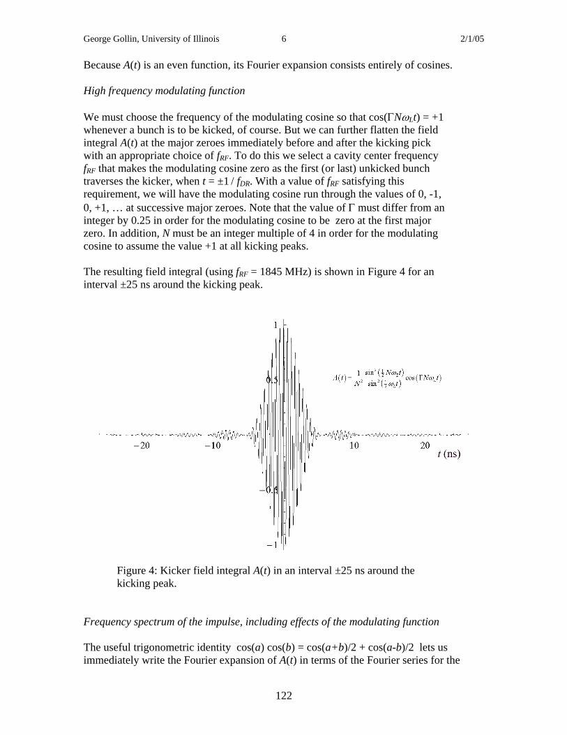
George Gollin, University of Illinois 6 2/1/05
Because A(t) is an even function, its Fourier expansion consists entirely of cosines. High frequency modulating function We must choose the frequency of the modulating cosine so that cos(ΓNωLt) = +1 whenever a bunch is to be kicked, of course. But we can further flatten the field integral A(t) at the major zeroes immediately before and after the kicking pick with an appropriate choice of fRF. To do this we select a cavity center frequency fRF that makes the modulating cosine zero as the first (or last) unkicked bunch traverses the kicker, when t = ±1 / fDR. With a value of fRF satisfying this requirement, we will have the modulating cosine run through the values of 0, -1, 0, +1, … at successive major zeroes. Note that the value of Γ must differ from an integer by 0.25 in order for the modulating cosine to be zero at the first major zero. In addition, N must be an integer multiple of 4 in order for the modulating cosine to assume the value +1 at all kicking peaks. The resulting field integral (using fRF = 1845 MHz) is shown in Figure 4 for an interval ±25 ns around the kicking peak.
Figure 4: Kicker field integral A(t) in an interval ±25 ns around the kicking peak.
Frequency spectrum of the impulse, including effects of the modulating function The useful trigonometric identity cos(a) cos(b) = cos(a+b)/2 + cos(a-b)/2 lets us immediately write the Fourier expansion of A(t) in terms of the Fourier series for the
122

George Gollin, University of Illinois 7 2/1/05
envelope function described above. A graph of the Fourier amplitudes of A(t) is shown in Figure 5. These amplitudes will yield a unit strength kicking pulse.
Figure 5: Fourier amplitudes of the field integral impulse A(t). The peak is at frequency fRF = 1845 MHz; the amplitudes become identically zero at fRF ± 180 MHz. These amplitudes will yield a unit strength kicking pulse.
Details of the kicking peak Figure 6 shows the kicking peak for the time interval (-50 ps, 50 ps). The shape is dominated by the high frequency modulation term cos(ΓNωLt). The kick drops rapidly away from its maximum at t = 0. This raises two separate issues. Is the kicker’s injection efficiency adequate? Are extracted bunches sufficiently free of kicker-induced distortion so that head-center-tail effects do not degrade the ILC’s luminosity? Recall that the RMS width of a damping ring bunch is ±20 ps. One promising strategy would be to install a corrector in the injection and extraction lines in order to compensate for the time dependence of the impulse delivered to a bunch. A single-frequency RF system running at fRF could deliver an impulse of the opposite sign to bunches shortly before/after injection/extraction. The residual error in kick after a corrector, shown in Figure 7, is about a third as large as the required kicker precision of 0.07%.
123

George Gollin, University of Illinois 8 2/1/05
Figure 6: Kicking peak in a time interval ± 50 ps around t = 0. RMS bunch length is 20 ps.
Figure 7: Fractional kick error, including an injection/extraction line corrector, in a time interval ± 50 ps around t = 0. Maximum allowable error is 0.0007, roughly three times the error at 50 ps.
124

George Gollin, University of Illinois 9 2/1/05
Modifications to the kicker RF system intended to flatten the kicking peak will generally increase the required amplifier bandwidth, through introduction of a low frequency tail, higher frequency bands in the vicinity of harmonics of the cavity center frequency, or both. Details of the major zeroes Figures 8a, 8b, 8c, and 8d show the impulse function in ±50 ps intervals around the first four major zeroes. Note that the choice of modulation frequency makes the error in the vicinity of the zeroes cycle through four different shapes: descending cubic, downwards quadratic, ascending cubic, and upwards quadratic. This may have the virtue of canceling some of the accumulated errors for bunches which make multiple passes through the kicker before being extracted. As it stands, the kick error when a bunch transits the kicker during a single orbit is small compared to the maximum allowable error of 0.0007. Details of this will depend on the tune of the damping ring.
Figure 8: Impulse function in a time interval ± 50 ps around the first four major zeroes. Note that the maximum allowable deviation from zero is .0007, substantially larger than the simulated kicker error.
125

George Gollin, University of Illinois 10 2/1/05
Low-Q cavity The Fourier series kicker needs to apply a ±10% bandwidth impulse to kicked bunches. It is an interesting technical challenge to devise a method to sum the effects of the various frequency components. An early (naïve!) conception of the kicker3 used one cavity for each frequency component, letting the beam sum the effects of the individual Fourier components. Another idea4, originally described by Joe Rogers, uses a low-Q cavity that can support the range of frequencies comprising the kicking pulse. Amplitude and phase lag of cavity response to driving signal We have not modeled the required cavity in any detail. In our simulations we assume it has Q = 25, is linear, and produces fields of adequate quality. We ignore the effects of reflections at its input port and describe the cavity’s response to a driving signal of frequency ω and amplitude Sdrive this way:
( ) ( )( )
( )2
22 2 00
cos cos2
drivecavity
SA t A t t
Q
ω ϕ ω ϕω ωω ω
= − = −⎛ ⎞
− + ⎜ ⎟⎝ ⎠
. (2)
Here ω0 is the cavity’s center frequency; the phase lag ϕ is defined as
( )
1 02 20
2tanQ
ω ωϕω ω
−⎛ ⎞⎜ ⎟≡⎜ ⎟−⎝ ⎠
. (3)
The ratio A(t)/Sdrive over the required bandwidth is shown in Figure 9. The phase lag ϕ is shown in Figure 10. (These are the equations describing the response of a damped, driven harmonic oscillator.) Fourier amplitudes and phases of driving signal arriving at the cavity Since the cavity stores energy and its response is frequency dependent, dividing the Fourier amplitudes shown in Figure 5 by the response function A(t)/Sdrive generates the distribution of Fourier amplitudes that must be delivered by the amplifier to the downstream end of the waveguide to generate a unit-strength kicking pulse. This spectrum is shown in Figure 11. (Bear in mind that we have not yet modeled the frequency-dependent transfer efficiency of power from the waveguide into the cavity.) The phase relationship between input and response changes considerably as the frequency crosses through resonance. Including the frequency-dependent phase of the
3 Ibid. 4 See, for example, George D. Gollin, Studies of Alternative TESLA Damping Ring Designs, http://www.hep.uiuc.edu/home/g-gollin/talks/AAC_damping_rings.pdf (2004).
126

George Gollin, University of Illinois 11 2/1/05
cavity response allows us to plot the required field as a function of time at the downstream end of the waveguide. This is shown in Figure 12.
Figure 9: Cavity response to driving fields, assuming a Q = 25 cavity with center frequency 1845 MHz.
Figure 10: Phase lag between cavity response and driving fields.
127

George Gollin, University of Illinois 12 2/1/05
Figure 11: Fourier amplitudes required at the downstream end of the waveguide to generate a unit-strength kicking peak in the RF cavity. The amplitudes were derived by dividing the coefficients in Figure 5 by the cavity’s frequency-dependent response.
Figure 12: Field at the downstream end of the waveguide that will generate a unit-strength kicking peak in the RF cavity. Note the difference in the maximum amplitude in the waveguide in comparison with the cavity field, shown in Figure 4.
128

George Gollin, University of Illinois 13 2/1/05
It is possible that the kicker system’s sensitivity to errors might be reduced (at the expense of greater input power) if the cavity center frequency were chosen to be above or below the kicking pulse’s frequency band. This is worth investigating in detail at a later time.
Waveguide We consider a rectangular waveguide with cutoff frequency fcutoff = 1300 MHz driven in its dominant mode5. The cutoff frequency depends on the waveguide’s geometry, shown schematically in Figure 13. When b > a, we have fcutoff = c/(2b), where c is the speed of light in vacuum. Our 1300 MHz waveguide has b ≈ 11.5 cm.
ab
x
y
z
Figure 13: Waveguide geometry. Power propagates in the +z direction. For this waveguide, fcutoff = c/(2b) = 1300 MHz.
Group velocity Besides providing a path between the amplifier and the RF structure, the waveguide serves as the dispersive transport that compresses the amplifier signal. The waveguide’s group velocity as a function of frequency is
2 2
1 1cutoff cutoffg
fv c c
fω
ω⎛ ⎞ ⎛ ⎞
= − = −⎜ ⎟ ⎜ ⎟⎝ ⎠ ⎝ ⎠
. (4)
Figures 14 and 15 show plots of vg(f) in the frequency ranges 0 to 4000 MHz and 1665 to 2025 MHz.
5 See, for example, Frank S. Crawford, Jr., Waves, Berkeley Physics Course—Volume 3, McGraw-Hill, New York (1968).
129

George Gollin, University of Illinois 14 2/1/05
Figure 14: Waveguide group velocity as a function of frequency in the range 0 to 4000 MHz.
Energy pumped into the upstream end of the waveguide will propagate down the guide with speed equal to the group velocity. Because vg(f) is frequency dependent, the relative phases of various Fourier components will vary with position along the length of the waveguide in a way that allows the delivery of a compressed pulse to the cavity.
Figure 15: Waveguide group velocity in the kicker’s frequency band, 1665 to 2025 MHz.
130

George Gollin, University of Illinois 15 2/1/05
Phase lag as a function of frequency and position Imagine that a single Fourier component with angular frequency ω is propagating in the z direction. We can write its amplitude at a fixed z position as acos[ω(t –tpropagation)]. The time delay tpropagation because power flows down the waveguide at the (finite) group velocity: we expect tpropagation = z/vg. Since the group velocity is frequency dependent, the propagation times for different Fourier components flowing through a waveguide will vary so that their relative phases at the end of the waveguide will be different from their initial values at the entrance to the waveguide. We have
( ) ( ) ( )1
2 2, 1propagation cutoffg
z zt zv c
ω ω ωω
−⎡ ⎤= = −⎢ ⎥⎣ ⎦
. (5)
The phase lag for a Fourier component of angular frequency ω relative to one of infinite frequency is, as a function of distance z along the waveguide,
( ) ( ) ( ) ( )1 1, , ,propagation propagation
g
z t z t z zv c
ϕ ω ω ω ωω
⎡ ⎤⎡ ⎤∆ = − ∞ = −⎢ ⎥⎣ ⎦
⎢ ⎥⎣ ⎦. (6)
The relative change in phase per meter of waveguide for adjacent Fourier components (separated in frequency by 3 MHz) is plotted in Figure 16. From the plot one can see, for example, that increasing the waveguide length by one meter will increase the phase lag of the 1800 MHz Fourier component by ~4° relative to that of the adjacent (1803 MHz) component. Shown in Figure 17a are plots of the field amplitudes in the waveguide as functions of time at z positions increased in 5 meter intervals. We have adjusted the graphs’ origins to keep the amplitude distributions near the center of each plot. The plots are presented in reverse time-order, with the compressed pulse at the downstream end of the waveguide appearing first. Figure 17b shows similar plots, but spaced at 20 meter intervals. Figure 17c is an enlarged version of the 80 meter plot from Figure 17b. Unusual features in the graphs are artifacts.
131

George Gollin, University of Illinois 16 2/1/05
Figure 16: Relative phase lag (in degrees) of adjacent Fourier components induced per meter of waveguide.
Notice that the peak power required from an amplifier at the upstream end of an 80-meter waveguide is not particularly different from the amplifier’s average power output. The field amplitude at the entrance to the waveguide is roughly one percent as large as the maximum field inside the RF kicking structure. We have not yet optimized the length or cutoff frequency of the waveguide. Operating with a cutoff frequency closer to the cavity’s center frequency would provide more dispersion per meter, allowing use of a shorter waveguide at the expense of greater sensitivity to inaccuracies in waveguide geometry.
132

George Gollin, University of Illinois 17 2/1/05
Figure 17a: Fields at different distances from the downstream end of the waveguide, shown as functions of time.
133

George Gollin, University of Illinois 18 2/1/05
Figure 17b: Fields at different distances from the downstream end of the waveguide, shown as functions of time.
134

George Gollin, University of Illinois 19 2/1/05
Figure 17c: Field 80 meters from the downstream end of the waveguide, shown as a function of time.
135

George Gollin, University of Illinois 20 2/1/05
Power amplifier We will assume that a 100 Gauss-meter impulse (3 MeV/c) is adequate. The kicking impulse under consideration requires an amplifier capable of generating signals in the frequency range (1800 ± 180) MHz. Estimate of required amplifier power Recall that the electric and magnetic fields in a resonant structure are 90° apart in phase. As a result, we can estimate the energy stored in the RF structure if we know its volume and the maximum electric or magnetic field it contains. Consider a generic RF device, shown schematically in Figure 18.
ab
x
y
z
L
Figure 18: Generic RF kicking structure. Beam travels along +z. The energy densities associated with electric and magnetic fields are ε0E2 and B2/µ0 when E and B are expressed in units of V/m and T. To inject or extract a bunch, the field strength in the kicker must satisfy 3 MeVE L ≥ or 0.01 T mB L ≥ ⋅ (7) Recall that the average values of sin(z) and sin2(z) over the interval (0,π) are 2/π and ½, respectively. If we assume the fields in the RF structure vary sinusoidally with z for a half wavelength along the structure’s length, we will have
2 2
12
2 2 2~
4E B
E B π
π= = (8)
so that
136

George Gollin, University of Illinois 21 2/1/05
2
2 3 MeV~4 L
E π ⎛ ⎞⎜ ⎟⎝ ⎠
and 2
2 0.01 T m~4 L
B π ⋅⎛ ⎞⎜ ⎟⎝ ⎠
. (9)
As a result, the energy stored in the RF device will be
12 4
2 2 00 0
0
9 10 10~ 62.54 4
ab ab abU abL E abL BL L L
πε πε µµ
−⋅ × ⋅= = = = . (10)
A device with a = b = 5 cm and L = 10 m will hold energy U = .015625 joules. Since the kicker is filled at 3 MHz, it requires 47 kW of RF power, neglecting losses and various coupling efficiencies. Note that the transverse electric field inside an RF structure of these dimensions is approximately 300 kV/m. Amplifier technology It appears that this power range, frequency and bandwidth suggest the use of a traveling wave tube amplifier (TWTA) rather than a klystron.6 We have not yet made more than a cursory investigation of technical issues associated with the choice of amplifier.
Programmable function generator We imagine driving the RF amplifier input with a programmable function generator. The device could be reprogrammed to compensate for drifts in the behavior of the amplifier, waveguide, and RF structure. We have not yet selected a commercial device with suitable properties.
What is missing We have not modeled the coupling efficiencies between amplifier and waveguide or waveguide and RF structure. It is possible that reflections at the coupler between the waveguide and the cavity will require a circulator to be installed in the waveguide. We have not studied the effects of losses in the waveguide, or of nonlinear behavior anywhere in the system. We have not yet simulated in detail the kicker’s effect on bunches that pass through it a number of times before being extracted.
Sensitivity to errors The TESLA Technical Design Report7 describes the maximum allowable kicker error as 0.07 Gauss-meters, both for bunches that are to pass through the kicker undisturbed
6 Ralph Pasquinelli, private communication. 7 TESLA Technical Design Report, http://tesla.desy.de/new_pages/TDR_CD/ (2001).
137

George Gollin, University of Illinois 22 2/1/05
(when its field integral is zero) and bunches that are to be extracted. Imperfections or drifts in amplifier performance, waveguide geometry, RF structure parameters, and bunch timing will all contribute to kicker performance errors. In this section we assume that injection and extraction line correctors are installed (as discussed previously) and describe the effects of various problems on kicker error. RF structure Q error The RF structure’s response to driving fields depends on Q: both the frequency dependence and the overall magnitude of the cavity fields are affected by an error in Q. Shown in Figure 19 are plots of the fractional kick error as functions of deviation in Q. The three curves correspond to the center, head, and tail of a bunch, assuming the “head” and “tail” positions are ±2.5σ (±50 ps) from the bunch center along the beam’s direction of travel. Full scale deviation in Q shown in the plot is ±0.1%, giving rise to fractional kick errors of approximately ±0.0006, slightly smaller than the maximum tolerable kick error of ±0.0007 (0.07%).
Figure 19. Fractional kick error caused by deviations in Q for the center (t = 0), head (t = -50 ps), and tail (t = +50 ps) of an extracted bunch.
The impulse error is smaller for unkicked bunches and is shown in Figure 20, in which comparisons of the effects on the kicked and first two unkicked bunches are plotted. The impulse error during an interval ±10 ns around the kicked bunch is shown in Figure 21.
138

George Gollin, University of Illinois 23 2/1/05
Figure 20. Kick error caused by deviations in Q for the center, head, and tail of the kicked and first two unkicked bunches. Full vertical scale corresponds to 0.07 Gauss-meters (2.1 keV/c).
Figure 21. Kick error as a function of time caused by a +0.1% deviation in Q. Note that bunches are only in the kicker at integral multiples of the damping ring bunch spacing, 5.56 ns in our model.
139

George Gollin, University of Illinois 24 2/1/05
RF structure center frequency error The RF structure’s response will be altered if its natural frequency deviates from the nominal value. The associated error in kicker impulse is shown in Figure 22 as a function of frequency deviation for the center, head, and tail of the kicked bunch.
Figure 22. Kick error as a function of cavity center frequency error (MHz).
Figure 23. Kick error as a function of cavity center frequency error for kicked, first unkicked, and second unkicked bunches.
140

George Gollin, University of Illinois 25 2/1/05
The effect is most significant for the head and tail of the kicked bunch; Figure 24 shows a graph of impulse error as a function of time for this bunch when the cavity center frequency is mistuned by 180 kHz (0.01%). Full horizontal scale in the plot is ±50 ps (±2.5σ).
Figure 24. Kick error as a function of time when the cavity center frequency is mistuned by 180 kHz (shown for the kicked bunch only).
Cavity mistuning should be maintained below 0.01% during operation. Waveguide length error Changes in the length of the waveguide will shift the arrival time of the kicking pulse at the cavity relative to the arrival time of a bunch, as well as shifting the relative phases of the different frequency components contributing to the kick. Both of these effects change the arrival time of the kick with the same sign. Figure 25 shows the effect of a 1 mm waveguide length error. The two curves represent the ideal and delivered impulses as functions of time; full scale in the plot is ±10 ps. Note the ~5 ps shift in the positions of the peaks. Since the waveguide’s group velocity is ~2/3 c in the kicker’s frequency band, we see that most of the shift in the location of the peak is caused by the overall increase in propagation distance, rather than the dispersion-induced shift in the relative phases of the Fourier components. This isn’t surprising: the phase difference between adjacent Fourier components only changes by a few degrees per meter of waveguide: a one millimeter length error will only shift their relative phases by a few thousandths of a degree. Most of the change in the time structure of the kicking peak comes about through its delayed arrival at the RF cavity.
141

George Gollin, University of Illinois 26 2/1/05
Figure 25. Effect of a 1 mm waveguide length error. The two curves represent the ideal and delivered impulses as functions of time; full scale in the plot is ±10 ps.
When the waveguide error is too large, the shape of the kicking peak will change so that the injection/extraction line correctors can no longer flatten the peak with sufficient accuracy. As a measure of this change in shape, we plot the difference between the delivered kick and an ideal impulse in Figure 26, in which the peaks of the delivered and ideal impulse curves have been aligned. Most of the deviation from the ideal impulse evident in Figure 26 is due to the difference in size of the delivered kick. Rescaling the kicks to have the same magnitude as the ideal impulse yields the curves plotted in Figure 27. This is encouraging: it would be sensible to build the waveguide to an accuracy in length of a centimeter or better, but it is easy to compensate for errors (or thermally induced changes) in length by tuning the amplitude and timing of the amplifier signal injected into the waveguide. The effect on unkicked bunches is also small, as can be seen in Figure 28. The effect on later unkicked bunches is even less than on the first unkicked bunch: as long as the waveguide length is controlled to an accuracy of a centimeter, adjusting the overall size and timing of the amplifier signal will compensate adequately for small changes in waveguide length.
142

George Gollin, University of Illinois 27 2/1/05
Figure 26. Effect of waveguide length error. Plotted are the differences between the delivered kicks and an ideal impulse for waveguides that are 5 mm, 10 mm, 15 mm, 20 mm, and 25 mm too long. The peaks in the delivered kicks have been shifted in time to align with the peak in the ideal impulse centered at t = 0.
Figure 27. Differences between delivered kicks and an ideal impulse for waveguides that are 5 mm, 10 mm, 15 mm, 20 mm, and 25 mm too long. The peaks in the kicks have been shifted in time to align with the peak in the ideal impulse that is centered at t = 0. In addition, the delivered kicks have been rescaled to have the same magnitude as the ideal impulse.
143

George Gollin, University of Illinois 28 2/1/05
Figure 28. Differences between delivered kicks and an ideal impulse at the arrival time of the first unkicked bunch for waveguides that are 5 mm, 10 mm, 15 mm, 20 mm, and 25 mm too long. The peaks in the kicks have been shifted in time to align with the peak in the ideal impulse that is centered at t = 0. The time region in the plot is centered on the arrival time of the first unkicked bunch. Waveguide cutoff frequency error Recall that the cutoff frequency for the rectangular waveguide shown in Figure 13 is fcutoff = c/(2b), where b is the larger of the waveguide’s transverse dimensions. Inaccuracies and thermal drifts in waveguide geometry will change the cutoff frequency, and therefore the frequency dependence of the group velocity. It should be possible to correct for this by reprogramming the function generator that drives the amplifier. The problems arising from drifts in cutoff frequency will be seen in a number of ways. The average group velocity will change, so the propagation time between amplifier and cavity will shift. This causes mistiming between the kicking peak and the beam. In addition, the phase differences between the various Fourier components arriving at the cavity are changed, leading to an error in pulse shape. How large an error in fcutoff might be tolerable? We can use the sensitivity to waveguide length errors as a rough indicator. Figures 25 - 28 suggest that a centimeter length change does not distort the pulse shape by an unacceptable amount. The relative phases of adjacent Fourier components change by a few hundredths of a degree per centimeter of waveguide, so we can ask what change in cutoff frequency might have a similar effect on the phases. After traveling the full length of the waveguide, frequency components separated by 3 MHz are split in phase by typically 300 degrees. As a result, a fractional error in error in group velocity, and therefore in cutoff frequency, that is small compared
144

George Gollin, University of Illinois 29 2/1/05
to a part in 104 ought to be tolerable. Since δvg/vg ~ δb/b, we will need the waveguide transverse dimension to be stable a few microns. To some extent we should see the same kinds of effects arising due to errors in waveguide cutoff frequency as we do with errors in length: there will be an overall time displacement of the kicking peak and a reduction in its amplitude, as well as distortion in the shapes of the impulse function in the vicinity of the zeroes. Some correction through adjustment of the timing and overall amplitude of the signal coming out of the function generator can (partially) compensate for this. The shift in arrival time of the kicking peak is shown in Figure 29 for a 100 kHz displacement in cutoff frequency away from the nominal value of 1.3 GHz. Note the ~30 ps displacement of the peak from t = 0.
Figure 29. Effect of a 100 kHz cutoff frequency error. The two curves represent the ideal and delivered impulses as functions of time; full scale in the plot is ±100 ps. Nominal fcutoff is 1.3 GHz.
The influence on the shape of the kicking peak is shown in Figure 30 in which we plot the difference between the delivered kick and an ideal impulse after the peaks of the delivered and ideal impulse curves have been aligned in time, and rescaled to have the same peak amplitude. The impact on the accuracy of the zero in impulse at the first unkicked bunch is shown in Figure 31. From these figures we see that it is harder to correct the impulse function at the first unkicked bunch than it is at the kicked bunch by rescaling and shifting in time: the impulse errors 50 ps away from the bunch centers are larger for the unkicked bunch. As it stands, this naïve correction scheme will be adequate for cutoff frequency errors smaller than about 20 kHz,
145

George Gollin, University of Illinois 30 2/1/05
Figure 30. Effects of cutoff frequency errors. The curves represent the difference between delivered and ideal impulses as functions of time after aligning the time of the peaks and rescaling the peak amplitudes. Full scale in the plot is ±100 ps. Nominal fcutoff is 1.3 GHz. Errors in cutoff frequency for individual curves are indicated on the plot.
Figure 31. Effects of cutoff frequency errors. The curves represent the difference between delivered and ideal impulses as functions of time. The peaks in the kicks have been shifted in time to align with the peak in the ideal impulse that is centered at t = 0. The time region in the plot is centered on the arrival time of the first unkicked bunch.
146

George Gollin, University of Illinois 31 2/1/05
Amplifier gain error: linear frequency dependence Any effect that causes the delivery of an incorrect set of amplitudes and phases for the various Fourier components to the RF structure will generate impulse errors. To see how sensitive the impulse function is to amplifier gain errors we model these errors assuming a linear frequency dependence: ∆G = α(f-fRF). Naturally, other forms of frequency dependence are possible! However, since we are working with a signal whose full bandwidth is only ±10% of its principal frequency, a linear model seems a sensible choice for the time being. How large can α become without overly distorting the impulse function? Figures 32, 33, and 34 show the consequences for α values of 0.5% per 180 MHz, 1.0% per 180 MHz, 1.5% per 180 MHz, and 2.0% per 180 MHz. In the plots, the impulse functions have been rescaled to agree in amplitude at t = 0 with the nominal kick. Full (horizontal) scale in the figures is ±100 ps. Since the full bandwidth in the impulse function is ±180 MHz, the different curves correspond to maximum deviations from ideal gain of ±0.5%, ±1.0%, ±1.5%, and ±2.0%. As before, it is the first unkicked bunch that is most susceptible to problems: amplifier gain errors (for errors that increase linearly with distance from the center frequency) should be kept smaller than ±1% over the full ±180 MHz band.
Figure 32. Effects of an amplifier gain error that grows linearly with frequency. The curves represent the difference between delivered and ideal impulses as functions of time. The time region in the plot is centered on the arrival time of the kicked bunch.
147

George Gollin, University of Illinois 32 2/1/05
Figure 33. Effects of an amplifier gain error that grows linearly with frequency. The curves represent the difference between delivered and ideal impulses as functions of time. The time region in the plot is centered on the arrival time of the first unkicked bunch.
Figure 34. Effects of an amplifier gain error that grows linearly with frequency. The curves represent the difference between delivered and ideal impulses as functions of time. The time region in the plot is centered on the arrival time of the second unkicked bunch.
148
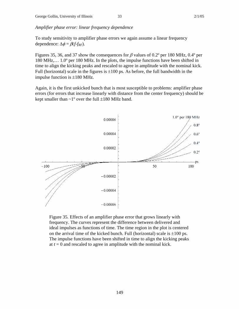
George Gollin, University of Illinois 33 2/1/05
Amplifier phase error: linear frequency dependence To study sensitivity to amplifier phase errors we again assume a linear frequency dependence: ∆φ = β(f-fRF). Figures 35, 36, and 37 show the consequences for β values of 0.2º per 180 MHz, 0.4º per 180 MHz,… 1.0º per 180 MHz. In the plots, the impulse functions have been shifted in time to align the kicking peaks and rescaled to agree in amplitude with the nominal kick. Full (horizontal) scale in the figures is ±100 ps. As before, the full bandwidth in the impulse function is ±180 MHz. Again, it is the first unkicked bunch that is most susceptible to problems: amplifier phase errors (for errors that increase linearly with distance from the center frequency) should be kept smaller than ~1º over the full ±180 MHz band.
Figure 35. Effects of an amplifier phase error that grows linearly with frequency. The curves represent the difference between delivered and ideal impulses as functions of time. The time region in the plot is centered on the arrival time of the kicked bunch. Full (horizontal) scale is ±100 ps. The impulse functions have been shifted in time to align the kicking peaks at t = 0 and rescaled to agree in amplitude with the nominal kick.
149

George Gollin, University of Illinois 34 2/1/05
Figure 36. Effects of an amplifier phase error that grows linearly with frequency. The curves represent the difference between delivered and ideal impulses as functions of time. The time region in the plot is centered on the arrival time of the first unkicked bunch.
Figure 37. Effects of an amplifier phase error that grows linearly with frequency. The curves represent the difference between delivered and ideal impulses as functions of time. The time region in the plot is centered on the arrival time of the second unkicked bunch.
150

George Gollin, University of Illinois 35 2/1/05
A comment on errors The errors in impulse function caused by the effects described above can be corrected through adjustment of the signal produced by the programmable function generator. Small corrections can be made through adjustment in overall amplitude and timing of the function generator signal; larger adjustments will require changing the mix of Fourier amplitudes and phases in the signal sent to the RF amplifier. Not all problems can be remedied through clever use of a low-level RF system to recognize impulse inaccuracies: noise and amplifier nonlinearities can introduce errors that cannot be removed through reprogramming.
Sensitivity to noise Amplifier noise We model amplifier noise as flat in frequency spectrum from 300 MHz to 6 GHz, and random in phase. We do not simulate noise outside this frequency range. To represent the noise voltage in the time domain, we divide the frequency band into bins that are 300 kHz wide and assign a noise voltage vi(t) = v0 cos(ωit + φi) to each bin. The subscript i labels the bin; the phase φi is selected randomly with no correlation between the phases of individual frequency bins. The overall noise voltage vnoise(t) is the sum of vi(t) over all bins i. As can be seen in Figure 17c, the maximum amplifier output is ~0.015 in units where the kicking voltage inside the RF cavity has unit strength 1. In these units, an RMS amplifier noise voltage of 10-4 per GHz1/2 produces the results shown in the next several graphs. Figure 38 illustrates a typical noise voltage, shown as a function of time, at the amplifier output. Note the presence of high frequency contributions to the noise amplitude. Since the RF cavity does not store energy efficiently at frequencies far from 1.8 GHz, we expect that the noise voltage inside the cavity will show much less out-of-band contribution than is present in the simulated amplifier noise. This can be seen in Figure 39 where the high frequency noise present in Figure 38 is largely absent. The noise distribution added to the kicking impulse corresponding to an amplifier noise level of 10-4 per GHz1/2 is shown in Figure 40. Note that the RMS noise voltage in the cavity is 0.00044 (in units where the ideal impulse has unit amplitude), somewhat smaller than the limit set by the total noise budget. The full bandwidth of the amplifier input signal is 360 MHz; restricted to this band, the rms noise associated with 10-4 per GHz1/2 would be 6×10⁻⁵ in comparison with a maximum signal of ~.015, or a required signal/noise ratio of ~250, or 48 db. With a wider acceptance band (the RF cavity responds to out-of-band frequencies), the required signal/noise ratio is greater.
151

George Gollin, University of Illinois 36 2/1/05
Figure 38. Effects of amplifier noise: the graph shows noise added to the amplifier’s output signal as a function of time over the time period ±10 ns. The amplifier is assumed to generate an RMS noise voltage of 10-4 per GHz1/2 in units where an ideal kick has unit amplitude. Noise is generated with constant amplitude and random phase in the frequency range 300 MHz to 6 GHz.
Figure 39. Effects of amplifier noise on kicking impulse: the graph shows the cavity’s response to the amplifier noise plotted in the previous figure. Note the absence of the high frequency components evident in the previous figure. RMS noise voltage in the cavity is 0.00044, in units where the ideal impulse has unit amplitude.
152

George Gollin, University of Illinois 37 2/1/05
Figure 40. Noise voltages. RMS width of the distribution is 0.00044, in units where the ideal impulse has unit amplitude.
Arbitrary function generator noise We do not yet model noise from the arbitrary function generator, instead including it in our naïve model for amplifier noise. It is reasonable to expect that the noise from a function generator will not be independent of frequency! Nonlinear effects Harmonic distortion Our modeling of harmonic distortion is primitive, and should be further developed. At the present time we assume that harmonic distortion introduces an unwanted contribution to the amplifier output that is only a function of the amplifier’s ideal (noise- and distortion-free) output signal as well as its output noise. We do not generate harmonic distortion associated with output frequency components introduced through other nonlinear effects such as intermodulation distortion. We do not model harmonic distortion arising from imperfections in the arbitrary function generator. As was done with the simulation of amplifier noise, we model amplifier harmonic distortion as flat in frequency spectrum from 300 MHz to 6 GHz. Only the first harmonic is generated, using a fixed phase relationship between the parent signal voltage and distortion-induced harmonic. This is more clearly (and concisely) described in equations:
( ) ( )
( ) ( )
1 1 1 1 11
1 1 1 1
cos cos
...where , and , .
n nn
n n n n
A t A n t
A A A A
ω ϕ ω ϕ δϕ
ω δϕ δϕ ω
∞
=
+ → + +
≡ ≡
∑ (11)
153

George Gollin, University of Illinois 38 2/1/05
In our model,
( ) ( )11 1 1 1
2 2, and ,
0 2 0 2n n
aA n b nA A A
n nω δϕ ω
= =⎧ ⎧= =⎨ ⎨> >⎩ ⎩
(12)
where a and b are constants. It would be natural to include more complicated dependences on amplitude and frequency; in the future we would like to refine these studies to incorporate more detailed properties of traveling wave tube amplifiers.
Figure 41. Voltages caused by (first) harmonic distortion. The coupling from fundamental into first harmonic is modeled to be independent of frequency as described in the text.
In our simple model, voltage arising from harmonic distortion scales linearly with a and shifts in time (without changing its shape) with b. Figure 41 illustrates the unwanted voltage added to an ideal signal in the case a = 0.5 and b = 0. In the figure contributions to the distortion signal from amplifier noise have been omitted: it seems likely that this is normally included in the quoted values of noise amplitude quoted by manufacturers of TWTA’s. The RF cavity response as a function of driving frequency was given in Equation 2. We see that the response to a driving signal at twice the center frequency ω0 is
154

George Gollin, University of Illinois 39 2/1/05
( )0
0
0
20
2222 2 0 20
2
2 2 0.027162 9
cavityAA
QQ QQ
ω ωω
ω ω
ω
ω ωω ω=
=
= ⎯⎯⎯→ ≈⎛ ⎞ +− + ⎜ ⎟⎝ ⎠
. (13)
Here
0Aω is the cavity’s response to a driving signal at its center frequency.
It is helpful that the cavity’s response to signals far from its center frequency is small! Since the principal signal’s full bandwidth is only ±10%, the distortion-induced harmonics are far from the signal band and are tolerable when a < 0.5, corresponding to -6dB. Intermodulation distortion Intermodulation (IM) distortion can introduce spurious signals at frequencies that are the sums and differences of frequencies present in the primary signal. As was true for harmonic distortion, the signal’s ±10% full bandwidth and cavity’s narrow frequency response will help suppress sensitivity to “second order” IM distortion. (Second order distortion signals primarily populate bands centered at 180 MHz and 3.69 GHz.) However, distortion-induced signals near 3.69 GHz can mix with signals in the primary band (centered at 1.845 GHz) to produce unwanted third order signals in the primary signal band. Our modeling of IM distortion is unsophisticated at the present time. We assume that voltages created through second-order IM distortion arise from the sum of the amplifier’s ideal signal, noise voltage, and harmonic distortion signal. We do not model IM distortion arising from imperfections in the arbitrary function generator. We calculate third-order harmonic distortion signals and then include them in the amplifier output presented to the simulation. We model amplifier couplings between different frequencies to produce IM distortion as flat in frequency spectrum from 300 MHz to 6 GHz, generating distortion signals at both the sum and difference frequencies. We describe the second order IM signals this way:
( ) ( ) ( ) ( )[ ]( ) [ ]( )
1 1 1 2 2 2 1 1 1 2 2 2
1 2 1 2
cos cos cos cos
cos cos
A t A t A t A t
A t A t
ω ϕ ω ϕ ω ϕ ω ϕ
ω ω ϕ ω ω ϕ+ + − −
+ + + → + + + +
+ + + − + (14)
In our model,
155

George Gollin, University of Illinois 40 2/1/05
( ) ( )
( ) ( )
1 21 1 2 2 1 2 1 2 1 1 2 2 1 2
1 21 1 2 2 1 2 1 2 1 1 2 2 1 2
, , , , and , , , , ,2
, , , , and , , , , , 2
A A A a A A A A b
A A A a A A A A b
ϕ ϕω ω ϕ ϕ ϕ ω ω ϕ ϕ
ϕ ϕω ω ϕ ϕ ϕ ω ω ϕ ϕ
+ + + +
− − − −
+⎛ ⎞− = = +⎜ ⎟⎝ ⎠
+⎛ ⎞− = = +⎜ ⎟⎝ ⎠
(15) where a+, a-, b+, and b- are constants. The same expressions are used to generate third-order IM distortion. Work on modeling of intermodulation distortion is in progress. Beam dynamics: effects associated with multiple passes through the kicker Most bunches pass through the kicker several times after injection, or before extraction. There are a variety of effects that enter into a calculation of the kicker’s influence on a bunch that orbits the damping ring several times during the injection/extraction cycle. In the extraction scheme under consideration, a bunch arrives at the kicker one “click” later each time it begins its next orbit of the damping ring until finally being ejected. As a result, it passes through the kicker during zeroes that are progressively closer to the kicking peak. In a naïve description of the damping ring, the effects on a bunch associated with multiple zero crossings would be unimportant due to the field integral’s zero first derivative. But imperfections in the kicker can introduce distortions to the impulse function that could cause coherent effects that will spoil beam emittance. Oscillations of the beam about a closed orbit, as well as the effects of synchrotron oscillations of particles inside the bunch relative to the bunch center, can be included in a beam dynamics simulation of the kicker. Prototyping and tests We have had discussions with Fermilab’s RF group and Technical Division about studies of some of the technical challenges associated with the Fourier series kicker. After our simulations are finished we will collaborate with the lab on the engineering studies necessary to see if the concept is workable. We have submitted an expression of interest8 to Fermilab to test devices in the A0 photoinjector beamline.
8 G.D. Gollin, M.J. Haney, and J.B. Williams, An Expression of Interest Concerning Investigation of TESLA Damping Ring Kickers using the A0 Photoinjector Beam, May 24, 2004, http://www.hep.uiuc.edu/home/g-gollin/Linear_collider/Fermilab_kicker_A0_proposal.pdf .
156

George Gollin, University of Illinois 41 2/1/05
UIUC Budget for LCRD 2.22 Item FY04 FY05 FY06 Summer + academic year salary, 2 undergraduates (assume 750 hours/year/student, $6.15/hr)
$9,225 $9,225 $9,225
Indirect costs on undergraduate salaries (53.05%) $4,894 $4,894 $4,894 Desktop computers for the students $6,000 - - Periodic student travel to Fermilab during summers $1500 $1500 $1500 Other travel (one trip to SLAC each year) $1,200 $1,200 $1,200 Totals $22,822 $16,822 $16,822
157

2.25
2.25
Accelerator Physics
2.25: Investigation and prototyping of fast kicker options for the TESLA damping rings
(progress report)
Accelerator Physics
Contact person Gerry Dugan
[email protected] (607) 255-5744
Institution(s)
Cornell
Funds awarded (DOE) FY04 award: 7,900
FY05 award: 135,000 FY06 award: 135,000
158

Investigation and prototyping of fast kicker options for theTESLA damping ring
April 11, 2005
Personnel and Institution(s) requesting funding
G. Dugan, D. Rubin, Laboratory of Elementary Particle Physics, Cornell University
Collaborators
D. Finley, C. Jensen, G. Krafczyk, V. Shiltsev, Fermilab
G. Gollin, T. Junk, University of Illinois at Urbana-Champaign
W. Decking, DESY
Project Leader
G. [email protected](607)-255-5744
1 Project Overview
The large number of bunches (2820) and the relatively large inter-bunch spacing (337 ns)in the TESLA linear collider design give a bunch train which is more than 200 km long.A damping ring of this size would be very costly, and so the bunch train is damped ina compressed form, with a bunch spacing of 20 ns, leading to a damping ring with acircumference of 17 km.
In the TESLA baseline, the rise and fall time of the damping ring injection and ex-traction kickers determine the circumference of the ring. There is considerable leveragein developing faster kickers, as this translates directly into a smaller circumference ring.The baseline system for 500 GeV (cm) parameters has a 20 ns specification for the kickerpulse width; this becomes about 12 ns for the 800 GeV (cm) parameters. Designs andprototype results exist [1] for conventional kickers with widths of 7 ns, and design havebeen developed for more novel ultrafast schemes [2] using electron beams.
We propose to further explore the feasibility of the kicker designs described in thereferences cited above, particularly the very fast stripline kicker[1]. We will also developnew ideas for fast kickers. For example, we will explore the possibility of the use of theponderomotive force from a high-intensity laser pulse to provide a very short kick to thebeam. We will work closely with our collaborators from the University of Illinois andFermilab in exploring their novel fast kicker concept.
In the TESLA baseline design, both the injection and extraction kickers must be fast.The injection kicker is considerably more difficult than the extraction kicker, because of
1
159

the larger beam size at injection. We will investigate the possibility of single-turn injectionof beam into the damping rings, which would eliminate the need for a fast injection kicker.
It should be noted that, in addition to the small pulse width (of order ns) required forthe kicker, extremely good pulse-to-pulse reproducibility is required in order to avoid beamjitter at the collision point. The fast intra-train feedback at TESLA cannot compensatefor pulse–to-pulse jitter introduced by the extraction kicker. Part of the evaluation of thefeasibility of any new kicker scheme must include an evaluation of the expected pulse-to-pulse jitter.
If a new fast kicker scheme is found to be technically feasible on paper, we propose todo an engineering design of a prototype, build the device, and test it using a high energyelectron beam.
If the development of a fast kicker is successful and the ring size can be reduced, theaverage current will go up and at some point multibunch beam stability becomes thelimiting factor to a further reduction in the ring size. This has been explored for twospecific cases in prior work [3], for an earlier set of TESLA beam parameters. We proposeto update and expand on these considerations, including our current understanding ofcritical stability issues such as the electron cloud, and to determine the minimum ring sizepermitted by beam dynamics considerations.
2 Progress Report
As noted above, the original proposal suggested that we would explore the physics issuesassociated with the use of damping rings of a much smaller circumference than the baselineTESLA TDR design, in order to determine the smallest feasible circumference for thedamping ring. This circumference determines the required rise and fall time for the kickers,which is a key element of the specification.
However, a number of other groups are also engaged in these physics studies. Given thenumber of researchers already addressing these issues, we felt that it would be more efficientto choose a circumference which is the smallest that one could realistically consider, and touse this to determine the rise and fall time requirements of the kickers. If a kicker could bebuilt to this specification, then it would easily serve for any larger circumference ring. Thisstrategy decouples the physics studies of the ring from the kicker development, allowingboth to proceed in parallel.
We have chosen a ring circumference of 3 km (similar to the PEP-II ring) as the smallestfeasible circumference, and focused on the development of a kicker, with its associatedpulser, appropriate for this ring. We assume the baseline ILC parameter of 2820 bunches.In a 3 km ring, these bunches, equally spaced, will have a 3.5 ns bunch spacing, so to allowthe injection and extraction of individual bunches, the overall time-dependent kick seen bythe beam must have a duration of less than 7 ns.
2
160

2.1 Specification for kicker and pulser
Bunch-by-bunch manipulation in a 3 km ring can be accomplished using a system ofstripline kickers (for an example of an early design, see[1]), driven by synchronized very fastpulsers, capable of delivering pulses in the multi-kV regime. The rise time and fall timesof the pulser can be about 0.5 ns, with a pulse width of about 4 ns. Individual bunchesmust be injected or extracted from the ring approximately once every 337 ns, forming atrain of 2820 bunches, with an overall train duration of about 1 ms. The train is injectedinto a linac for subsequent acceleration. This process is repeated at a cycle rate of 5 Hz.
2.1.1 Kicker
As the basic module of the kicker, we consider a 0.36 m long stripline kicker, similar tothat described in [1]. The kicker can be represented essentially as a vacuum parallel-platetransmission line, and can be designed to have an impedance in the range of 50-100 Ω.It will be terminated in its characteristic impedance, to suppress any reflections. Twosynchronized pulses, of opposite polarity, injected onto the stripline plates at one end ofthis line, traveling opposite to the beam, will deliver a transverse kick to the beam. SeeFig. 1 for a schematic illustration of the kicker. The cross section of a prototype design isshown in Fig. 2
−V(s,t)
0
Beam particlev
x
y
EBc
s
x
l
Z
Z
V(s,t)
Figure 1: Stripline kicker
In Fig. 3, a possible pulse waveform is given, together with the resulting time variation
3
161

0
y
x
h=35 mm
w=50 mm
V=−V0
Positron beam: rms radius 7 mm at injection, beta=50 m
V=V
Figure 2: Stripline kicker cross section. The kicker is 360 mm long.
of the kick. The pulse rise time and fall time (10% to 90%) is 0.64 ns, and the pulse flat top(90% to 90%) is 2.96 ns. The time-dependent kick, K(t), is related to the voltage pulse,V (t), by
K(t) ∝∫ t+tk
t−tk
V (t′)dt′,
in which tk is the length of the stripline, which is 1.2 ns in this case. The time-dependentkick has rise and fall time (10% to 90%) of 1.97 ns, and the kick flat top (90% to 90%) is1.63 ns. This time-dependent kick at ±3.5 ns is 0.09% of the peak value, so it satisfies therequirement of being less than 7 ns in duration.
Note that other shapes are possible for the pulse, provided that the overall durationof the kick is less than 7 ns, and there is a flat-top for K(t) of duration at least equal tothe duration of the beam bunch (20 ps) plus any timing synchronization jitter betweenthe pulsers. Generally, the overall pulse duration will need to be roughly at least 2tk inorder for the kicker to be fully efficient. This is because the pulse must be long enough tocompletely fill the kicker before the beam enters (tk) plus it must remain there during thebeam’s passage (another tk.)
4
162

-4 -2 2 4t HnsL
0.2
0.4
0.6
0.8
1
Pulse amplitude
1 2 3 4 5 6Ω HGHzL
-0.25
0.25
0.5
0.75
1
1.25
Pulse amplitude Fourier harmonic
-4 -2 2 4t HnsL
0.2
0.4
0.6
0.8
1
Kick amplitude
Figure 3: Top, symmetric pulse, V (t). The pulse rise and fall time (10% to 90%) is 0.64ns, and the pulse flat top (90% to 90%) is 2.96 ns. Center, Fourier spectrum of the voltagepulse V (t). Bottom, resulting time-dependent kick, K(t). The kick rise and fall time (10%to 90%) is 1.97 ns, and the kick flat top (90% to 90%) is 1.63 ns.
2.1.2 Time structure of a pulse train
The pulses described in the previous section must be delivered to the fast kicker with apulse train structure illustrated in Fig. 4. The pulses are separated by 337 ns, and occur
5
163

in a train of 2820 successive pulses, with a total duration of 0.950 ms. The burst pulserate during this train is 2.97 MHz. These trains are separated by a gap of 200 ms; i.e., thetrain rate is 5 Hz. The average pulse rate is 2820× 5 = 14, 100 Hz.
t
................................... ............. ......................337 ns
0.95 ms2820 pulses
200 ms
Figure 4: Pulse train structure. The pulses are separated by 337 ns, and occur in a trainof 2820 successive pulses, with a total duration of 0.950 ms. The burst pulse rate duringthis train is 2.97 MHz. These trains are separated by a gap of 200 ms; i.e., the train rateis 5 Hz. The average pulse rate is 2820× 5 = 14, 100 Hz.
2.1.3 Pulse voltage, current, and synchronization requirements
The overall requirement for the system of fast kickers is to deliver a kick of 0.6 mrad to a5 GeV electron beam. The kick angle is related to the kicker parameters by
θ =2eV0
mc2
l
h
1γ
tanhπw
2h,
in which V0 is the kicker voltage (per electrode), l is the kicker length, h is the kickerhalf-gap, w is the half-width of the electrodes, and E = γmc2 is beam energy. For theexample considered here, h = 35 mm, w = 50 mm, and E = 5 GeV.
The length l of a single kicker module is constrained due to the requirement for a rapidrise time. Consequently, a number Nk of kickers will be required in series. The pulsers forthese kickers must be synchronized, as is the case for the two pulsers which drive a singlekicker, as discussed in Section 2.1.1.
In Table 1, two possible sets of pulser voltage, current, and power parameters are given,one corresponding to 3 kV pulses, and one to 10 kV pulses. In the former case, 50 kickers(100 pulsers) are required. In the latter case, 15 kickers (30 pulsers) are needed. The 10kV pulser dissipates about 100 W in the terminating load. If higher voltages than 10 kVare available, such a pulser, which requires even fewer kickers than 15, would be preferable.
2.1.4 Pulse-to-pulse stability requirements
In a given pulse train, the relative pulse-to-pulse repeatability requirement on the total kickangle given to a beam bunch is 7 × 10⁻⁴. If Nk kickers are used, and the pulsers driving
6
164

Table 1: Possible fast kicker parameters. The total kick angle required is taken to be 0.6mrad. The kicker is assumed to have a 50 Ω impedance. The voltage V0 refers to the peakamplitude of the voltage pulse V (t).V0 [kV] l [mm] θ[mrad] Nk I [A] Ppeak [kW] Epulse [mJ] favg [kHz] Pavg [W]
3.0 360 0.012 50 60 90 0.648 14.1 9.210.0 360 0.040 15 200 2000 7.2 14.1 102
each kicker have random voltage fluctuations about an average over the train, with an rmsvalue of σV , then we require
σV 6√
Nk × 7× 10⁻⁴.
For example, for the case of Nk = 15, we need σV 6 0.27%.In addition, in order to not disturb the neighboring bunches, the amplitude of the kick
K(t) at the time of the neighboring bunches must be less than 0.3% of the peak kickamplitude.
2.2 Implementation of the fast pulser
To implement the fast pulser, we need a very fast rise and fall time device, capable ofdelivering voltage pulses in the kilovolt range, with an burst pulse repetition frequency of3 MHz, capable of 1 ms bursts at 5 Hz, and extremely high pulse-to-pulse reproductibility.Meeting these demanding requirements is very challenging. Compared to gas-filled ampli-fiers, solid-state devices can potentially have very good reliability and reproducibility, buthave difficulty meeting the high-power-pulse rise and fall time requirements.
We have begun to investigate a relatively new high-power ultra-fast-switch technology,based on a 4-element npnp structure called a fast ionization dynistor[4, 5, 6, 7, 8, 9, 10, 11,12]. Ultra-fast high voltage pulse generators based on this technology are now commerciallyavailable[13, 14]. We have contacted a commercial firm, FID Technology, Ltd., whichmakes these pulse generators, and made them aware of the pulser requirements discussedin Section 2.1. They have responded with several sets of possible pulser specifications thatthey feel they can meet. These are presented in Table 2.
After much discussion, we focused on the pulser FPG2-3000-MC2, to procure as aprototype. It has specifications are close to what is required. The pulse is asymmetric,with the fall time being somewhat longer than the rise time. Nevertheless, the resultingtime-dependent kick may be acceptable. A model of an asymmetric pulse having featuressimilar to those of the FID pulser, and the resulting time-dependent kick, is shown inFig. 5. The details of rise and fall times for this model are given in Table 3.
Pulses from a 4 kV pulser built by FID Technology, for another application, illustratingthe achievable rapid rise and fall times, are shown in Fig. 6 and Fig. 7.
We have ordered the pulser FPG2-3000-MC2 from FID Technology, using a combination
7
165

Table 2: FID Technology Pulser Specifications[15]Pulser FPG2- FPG1- FPG3- FPG10-
3000-MC2 3000 3000 3000Output impedance[Ω] 50 100 100 100
Maximum output per channel [kV] ±1 1 3 10Number of channels 2 1 1 1
Rise time 10-90% of amplitude [ns] 0.6-0.7 0.6-0.7 0.6-0.7 0.6-0.7Pulse duration at 90% of maximum [ns] 2-2.5 2.5-3 2.5-3 2.5-3
Fall time 90-10% of amplitude [ns] 1-1.5 1-1.5 1-1.5 1.2-1.7Maximum PRF in burst mode [MHz] 3 3 3 3
Maximum PRF in continuous mode [kHz] 15 15 15 15Triggering - internal, external 5-10 v [ns] 20 20 100 100Amplitude stability in burst mode [%] 0.3-0.5
Pre- and after-pulses [%] 0.3-0.5Timing jitter, relative to trigger [ps] 20
Table 3: Timing features of calculated symmetric and asymmetric pulses and kicksFeature Symmetric Asymmetric
Pulse rise time (10% to 90%) [ns] 0.64 0.64Pulse flat top (90% to 90%) [ns] 2.96 2.40Pulse fall time (90% to 10%) [ns] 0.64 1.15Kick rise time (10% to 90%) [ns] 1.97 1.91Kick flat top (90% to 90%) [ns] 1.63 1.0Kick fall time (90% to 10%) [ns] 1.97 2.1
Kick at 3.5 ns/Peak kick [%] 0.088 0.09
of funding from this proposal and from other sources. Delivery is estimated for June orJuly, 2005.
2.3 Future plans
Once the prototype pulser described above arrives, we will test it with a 50 Ω dummy load,and check that the performance specifications are met. In particular, we will measure theamplitude stability, and the pre- and after-pulse levels, as well as the detailed shape of thecurrent pulse.
Subsequently, we are currently planning to test the pulser on a 100 Ω stripline kickerwhich has been built by Fermilab and the University of Illinois. This stripline kicker willbe installed in the 16 MeV electron beam at the Fermilab A0 photoinjector facility. Mea-surements of the kick delivered by the pulser to the beam will allow the time-dependence
8
166

-4 -2 2 4t HnsL
0.2
0.4
0.6
0.8
1
Pulse amplitude
-4 -2 2 4t HnsL
0.2
0.4
0.6
0.8
1
Kick amplitude
Figure 5: Top, symmetric pulse (black) and asymmetric pulse (red) V (t). Bottom, resultingtime-dependent kick, K(t), in both cases. The timing features of the pulse and the kickare given in Table 3.
of the kick to be studied in detail.Provided that the FID pulser performs according to requirements, we will continue
development of the fast kicker system as planned in the original proposal. We will builda 50 Ω kicker, suitable for the ILC damping ring, along the lines of the design describedabove. We will procure a higher voltage FID pulser, probably in the ±5 kV range. We willtest this kicker-pulser combination, which will be a true prototype for the ILC dampingring system, using the electron beam from the Cornell linac.
9
167

Figure 6: 4 kV fast pulse from FID Technology pulser[15] Rise time (10% to 90%): 0.4 ns.Flat top (90% to 90%): 0.9 ns. Fall time (90% to 10%): 1.1 ns
Figure 7: 4 kV fast pulse from FID Technology pulser. [15]
10
168

References
[1] B. I. Grishanov et. al., “Very Fast Kicker for Accelerator Applications”, TESLA 96-11(Nov., 1996)
[2] V. Shiltsev, “Beam-beam Kicker for Superfast Bunch Handling”, NIM A374, p. 137(1996)
[3] V. Shiltsev, “TESLA Damping Ring Impedances: Preliminary Design Consideration”,TESLA note 96-02 (1996)
[4] V. M. Efanaov et. al., “New superfast power closing switched-dynistors on delayedionization”, in Proceedings of the 1996 International Power Modulator Conference,pp. 22-25,
[5] V. M. Efanaov et. al., “Powerful Semiconductor 80 kV Nanosecond Pulser”, in Pro-ceedings of the 11th International Pulsed Power Conference, pp. 985-987
[6] I. V. Grehkov et. al., “Physical Basis for High-Power Semiconductor NanosecondOpening Switcher”, in IEEE Transactions on Plasma Science, Vol. 28, No. 5, pp.1540-1544 (Oct, 2000)
[7] T. M. Podlesak, “Single Shot and Burst Repetitive Operation of Thryristors for Elec-tric Launch Operations”, in IEEE Transactions on Magnetics, Vol. 37, No. 1, pp.385-388 (Jan, 2001)
[8] P. Rodin et. al. , “Tunneling-assisted impact ionization fronts in semiconductors ”,Journal of Applied Physics, Vol. 92, No. 2, pp. 958-965 (July, 2002)
[9] P. Rodin et. al. , “Superfast fronts of impact ionization in initially unbiased layeredsemiconductor structures”, Journal of Applied Physics, Vol. 92, No. 4, pp. 1971-1981(Aug., 2002)
[10] I. V. Grehkov et. al., “High Power Semiconductor-based Nano and SubnanosecondPulse Generators with Low Delay Time ”, in Proceedings of the 2004 Power ModulatorConference, ,O-SS Sw 4-7
[11] V. M. Efanaov et. al., “FID Solid State Switches with Gigawatt Peak Power ”, inProceedings of the 2004 Power Modulator Conference, O-SS Sw 4-8
[12] 2nd European Pulsed Power Symposium (See booklet of abstracts, pp. 36, 42, 47)
[13] FID Technology
[14] MegaPulse, Pulse Systems group
[15] V. M. Efanaov, B. O’Meara, private communication
11
169

2.26
2.26
Accelerator Physics
2.26: Continuing Research and Development of Linac and Final Doublet
Girder Movers
(new proposal)
Accelerator Physics
Contact person David Warner
[email protected] (970) 491-1035
Institution(s)
Colorado State SLAC
New funds requested FY05 request: 57,000 FY06 request: 66,400 FY07 request: 58,400
170

Continuing Research and Development of
Linac and Final Doublet Girder Movers
Classification: Accelerator Science Institution and Personnel requesting funding: Colorado State University David W. Warner, Engineer Collaborators: Stanford Linear Accelerator Center: Gordon Bowden (staff scientist) Project Leader: David W. Warner [email protected] (970) 491-1035 Project Overview This proposal is a continuation of the magnet mover R&D which was supported in the 2003 LCRD program. The project was not selected for funding in the 2004 round of LCRD grants, but we were given a no-cost extension to our existing grant and strongly encouraged to apply again in the next round. This extension has allowed us to continue research at a very low level. We are requesting funds for a three-year R&D program, which will continue our investigations of the resolution attainable with mechanical movers similar to those produced at SLAC for the FFTB, and our efforts to reduce the costs associated with manufacturing them. We will also mount piezoelectric movers to the FFTB magnet mover to possibly reduce cost and/or improve the precision of the design while maintaining the required range of motion. After selecting the optimal design choice, we will produce production mover designs and a prototype device, with an emphasis on manufacturability and cost reduction. Vibration isolation and temperature control requirements are beyond the scope of this project—we are investigating the feasibility of manufacturing movers capable of meeting the motion precision required by the accelerator.
171

Two important decisions taken in the last year have had a major impact on magnet mover requirements. First, the selection of cryogenic RF technology for the linac has reduced the number of magnet movers required. Rather than the approximately 10,000 movers which would have been required for the full linac, we are now developing movers for only the warm magnets used in the beam delivery system of the accelerator, which will require approximately 1000 movers. The reduction in the number of movers has lowered the relative importance of cost while increasing the importance of performance. We are in the process of re-evaluating our initial plans in light of this change in requirements. Second, the requirement for 10nm step size for the final focus girder movers has been changed to 50nm, allowing us to use the same basic mover design throughout the beam delivery system. Basic Mover Requirements
Every magnet and structure girder in the ILC beam delivery system will sit on movers to allow it to be positioned accurately. Depending on the requirements of the component in question, the movers will be required to position the beam components in either three degrees of freedom (two linear positions and one angle) or five degrees of freedom (two linear positions and three angles). Beam delivery system movers will typically be adjusted every few minutes, and must have a resolution or “step size” of approximately 50nm. It is not required that each step be precisely 50nm, simply that the average step size over a series of 10-20 steps achieve this limit. The movement will be relative, with the motion required by the mover and achieved in operation determined by beam position monitors. Since approximately 1,000 movers will be required, cost reduction, manufacturability and reliability are important for this component.
Gordon Bowden has developed and produced movers used in the FFTB which have been demonstrated to meet the requirements for final focus component movers except for resolution (they were measured to achieve a position resolution of approximately 300nm) and cost (a 5-degree of freedom mover would probably cost at least $5000 each to manufacture in their current design, at least in small quantities). These movers are mechanical, utilizing a kinematic support concept providing motion by rotation of bearings mounted on an eccentric shaft, which are in contact with wedge-shaped anvils supporting the linac component (See Fig. 1). Rotation of the shaft is accomplished by means of a 200 step per rotation stepper motor driven through a 100:1 harmonic drive. Mechanical movers such as these have several desirable features, including potentially lower cost (due to reduced requirements for feedback and control circuitry), reliability, and the ability to retain a set point without active compensation. Position monitoring can be accomplished by simply mounting a rotary encoder on the shaft.
172

Figures 1A and B: Magnet mover prototype built at CSU from modified SLAC drawings
In order to meet the 50 nm step size requirement, the rotation of the eccentric shaft must be controlled in approximately 60 microradian intervals, or about 100,000 steps per rotation. This is challenging. One possibility for achieving the desired position resolution with the existing mover design is to increase the step resolution of the stepper motor to at least 2000 steps per rotation with a micro-step motor controller. This concept remains untried, and testing is required to determine if a purely mechanical mover of this type can provide 50 nm resolution.
The stepper motors and the harmonic drives are the cost drivers for this system. Any cost reduction effort for the mover must begin here. One way to accomplish this is to use stepper motors more efficiently, with less expensive mechanical reduction to replace the harmonic drives. It may even be possible to eliminate the mechanical gear reduction altogether, if it is possible to drive the stepper motor itself with sufficient precision and maintain sufficient stopped torque from the stepper motor. A second option is to use the mechanical mover to achieve rough positioning (with micron-scale precision) and achieve the 50nm precision motion using piezoelectric stacks. A final option is to use other mechanical options for driving the shafts with the required precision, such as DC actuators or combinations of stepper motors with worm gears, vertical wedges, piezoelectric inchworm movers or other systems.
Broader Impact and Student Involvement This project will involve both graduate and undergraduate students in developing and testing the LabVIEW control software used to actuate the stepper motors and also the motion control software required to change the rotational motion of the shafts into physical motion of the magnet through two linear and three angular degrees of freedom. The precision movers developed for this project may be useful for other accelerator projects, as well as for optics and other high precision applications.
173

Results of Prior Research In September 2003 the Technical Design facility at CSU received funds from the Linear Collider R&D program to develop linac magnet movers and final doublet girder movers. At that time, work began on procuring a prototype mover, refining our understanding of metrology techniques which will be used to qualify the mover, and exploring other shaft drive options that might prove more cost-effective. Our request for continued funding as part of the 2004 LCRD program was not supported, although a no-cost extension to our existing LCRD grant was approved allowing us to continue work on this project at a greatly reduced rate. In the past year we have built a prototype mechanical mover system and are currently working on the stepper motor microstep control system and rotational encoder systems. We have made progress in identifying candidate metrology systems, but are awaiting the results of this funding request before reaching a decision on the extent of the system we will purchase. Prototype mover system: Unfortunately it was not possible to get an existing mover from SLAC, so we have replicated a modified version based on the original design and drawings for the SLAC three-axis mover. Our variant initially includes only three motors (as in the original FFTB mover), which will allow us to control two linear dimensions and one angle (X and Y and roll), but our model was designed to be expanded to 5 motors, allowing us to control all three angles (Pitch, yaw and roll) and two linear dimensions (X and Y, not along the beam axis). The prototype mover combines harmonic drive reducers and a micro-stepped stepper motor to drive the mount shafts, which should allow us to achieve the required step resolution. Stepper Motor & Control System: We have purchased and are studying the performance of a stepper motor system using Lin Engineering Model 5704M stepper motors, with a resolution of 0.45 degrees per step, or 800 steps/revolution. These motors are driven with Intelligent Motion Systems Inc. IM483 microstep drivers, which have a published resolution of 256 microsteps per full step. The combination of the motor and driver gives us a theoretical resolution of 204,800 microsteps per revolution. Using this motor/driver combination, it may be possible to eliminate the mechanical harmonic drive mechanical step reduction. If we can achieve sufficient precision and torque to drive the system, this would be a great simplification to mechanical assembly and cost. The rotational position of the drive shafts is measured using a Micro-E Chip Encoder, with a resolution of 163,840 counts/revolution, allowing angular measurement with the required precision.
174

In preliminary bench-top testing we achieved very nearly the theoretically predicted precision through a small (few hundred) number of microsteps, but the rotation became less accurate as larger numbers of steps were moved. After further investigation it was determined that driver cards were a major source of our difficulties, due to electronic noise generated as the micro step driver crossed a full step boundary for the stepper motor. We are replacing them with a new model recommended by Lin Engineering, and expect better performance from our new system. In addition to replacing the drivers as mentioned above we plan to acquire a Trinamic TMCM-302 3-axis controller. This controller will act as the interface between the drivers, encoders and a PC running Labview software.
Metrology:
We are investigating a metrology system based on capacitive position measuring, using a system from Lion Precision that will allow measurements with a precision of approximately 10 nm over a range of 50 microns. Additionally, each of the five drive shafts (after harmonic drive reduction) will be read out using rotary encoders with 3mr resolution. Together, this will allow us to measure the entire range of motion of the mover. We are also investigating linear encoder measuring systems such as those available from RSF electronics, which can achieve a resolution of approximately 100 nm.
We have a quote on a one sensor system that we will buy for our initial measurements, and plan to expand to a full 5 sensor system after we have proven the system works.
This metrology is for use in testing our prototype movers, and would not be part of a production design.
Facilities, Equipment and Other Resources
Our proposal is greatly enhanced by the mover prototype already funded by earlier LCRD funds. Our group also has significant experience with PC-based control systems and experienced LabVIEW programmers. We also have sufficient laboratory space with power, internet access etc. and low cost access to a machine shop with precision lathes, milling machines, etc., provided by the university.
This project is an excellent fit to the capabilities of the technical design facility at Colorado State University. The facility has been involved in manufacturing many components for HEP applications that require cost optimization due to the large number of items to be procured, as well as a great deal of prototype development and fixturing work. Through Prof. Wilson, the CSU HEP group has a long history of participation in the Linear Collider Detector development. The group is fully supportive of the technical design facility proposals to contribute to Linear Collider Accelerator development. Additionally, there is a precision measurements group in the department working on laser atom lithography projects lead by Prof. Siu Au Lee, which can provide advice and assistance as required.
175

Proposed Project
The work already funded by the LCRD program in our first proposal will be completed by the end of the summer of 2005. Our new proposal expands on the work already funded, taking advantage of the FFTB mover and metrology equipment we will build, and the experience we will have gained to move towards final mover designs. Year one of this new proposal continues the initial project, investigating rotary motion drivers and motion encoders in an attempt to find a cost-effective version of the FFTB mover with sufficient resolution. We now have an operational mechanical prototype, and shortly will have the micro-stepped stepper motors in place and tested. We also hope to have the metrology equipment in place to allow us to measure its motion by early summer 2005. By October 2005, we will have determined if we can meet the step resolution required with a mechanical three-motor microstepped mover, what type of rotation reduction system will be required, and a preliminary indication of the cost per mover and the difficulties in producing this type of mover A LabVIEW-based control system and motion control software will be developed with student assistance to allow us to move the magnet platform through a specified range of motion. Additionally, we plan to purchase a full 5-axis capacitive position measuring system (actually an expansion of the system we are ordering for 1-axis measurements under our current grant) in order to be able to fully monitor the 5-axis movement of the stage simultaneously. Deliverables:
-Measurements of the resolution achievable using the micro-step driven FFTB mover, both for three-motor and five-motor configurations. -Development of a metrology system capable of measuring the 5-axis motion of the mover with better than 50 nm precision. -Results from feasibility of alternate shaft driver options. -Software and hardware for mover control system
-Designs for magnet mounts for a five-motor system Year two goals are to evaluate the incorporation of piezoelectric movers and active feedback into a reduced-precision mechanical mover, with feedback based on the capacitive metrology system we are investigating for measuring the system performance or strain gauges. Our experience during the first year of the project will give us a solid understanding of the limitations of the mechanical mover, and based on this platform we will develop a piezoelectric stack to attach to the mover, and begin to investigate the resolution, vibration isolation, and stability achievable with such a system.
176

Additionally, we will investigate the possibility of using other mechanical movement devices or alternate motor options, such as DC actuators or piezoelectric inchworm devices to try to reduce costs by eliminating the harmonic drive. Deliverables:
-A design for a feedback system to stabilize a piezoelectric stack add-on to a mechanical mover capable of achieving 50 nm precision. -A prototype mover system including these additions, and measurements of the resolution and stability achievable by such a system.
Year three of the project will move towards manufacturability of the beam delivery system mover at a low price, involving redesign of the components in collaboration with manufacturing firms to reduce price and to determine the most cost effective option for the driver system. Year three will also include development of any special mounts required for the final focus girder cryostat.
Deliverables:
-An optimized-for-manufacturability design report for the beam line movers, including an optimized shaft driving system, measurements of system performance, and projected costs -A design for a final focus element mover.
Budget Justification There is no HEP base program grant support for Warner. All costs, including travel, associated with this proposal must be provided by the project. Warner’s salary is charged through the CSU Technical Design Facility at a flat rate of $50/hour. Fringe benefits charges are included in this hourly rate. Technician support and machine shop labor are also charged at flat hourly rates of $30/hour and $33/hour respectively, with fringe included in these rates as well. In Year 1 (FY 05) our labor costs include: 2.5 months support for Warner; technical support funds in the form of machine shop and technician time for additional prototype development work; and summer salary support for a one graduate student to assist with control software development and system testing. We are requesting equipment and M&S funding for the metrology system, computer control hardware, and continued stepper motor development costs. We are requesting travel funds to support 3 trips, typically to SLAC and/or FNAL, to consult with LINAC development experts and report results. In Year 2 (FY 06) our labor costs include: 3 months support for Warner; technician support; and summer salary for one grad student to assist with measurements and metrology software improvements. We are requesting equipment support for the piezo-electric mover; this equipment cost includes labor (including undergraduate student
177

labor), materials and supplies, but will be capitalized as a single piece of equipment at CSU. We are requesting travel funds to support 3 trips, typically to SLAC and/or FNAL. In Year 3 (FY 07) our labor costs include: 3 months support for Warner; and technician support for testing the mechanical prototype. We are requesting equipment funds to build an industrial prototype mover in conjunction with a local manufacturing firm; as Year 2, this equipment cost includes development and M&S expenses (including undergraduate student labor) which will be capitalized as a single piece of equipment. We are requesting travel funds to support 3 trips, typically to SLAC and/or FNAL. Three-Year Budget, in then-year K$
Item FY2005 FY2006 FY2007 TotalOther Professionals 26.8 33.0 28.5 88.3Graduate Students 4.5 4.5 0.0 9.0
Undergraduate Students 0.0 0.0 0.0 0.0Total salaries & Wages 31.3 37.5 28.5 97.3
Fringe Benefits 0.2 0.2 0.0 0.3Total Salaries, Wages and Fringe Benefits 31.5 37.7 28.5 97.6
Equipment 14.0 12.0 16.0 42.0Travel 1.5 1.5 1.5 4.5
Materials and Supplies 0.0 2.5 2.5 5.0Other Direct Costs 0.0 0.0 0.0 0.0Total Direct Costs 47.0 53.7 48.5 149.1
Indirect Costs 10.1 12.7 9.9 32.7Total Direct and Indirect Costs 57.0 66.4 58.4 181.8
178

2.27
2.27
Accelerator Physics
2.27: Effects of CSR in Linear Collider Systems: A Progress Report
(progress report)
Accelerator Physics
Contact person James Ellison
[email protected] (505) 277-4613
Institution(s) New Mexico
Funds awarded (DOE)
FY04 award: 36,758 FY05 award: 36,758 FY06 award: 36,758
179

Effects of CSR in Linear Collider Systems:
A Progress Report
Classification (subsystem)
Accelerator
Personnel and Institution(s) requesting funding
James A. Ellison, Professor of Mathematics, U. of New Mexico
Gabriele Bassi, PostDoc, Mathematics Department, U. of New Mexico
Klaus Heinemann, Research Assistant, Mathematics Department, U. of New Mexico
Collaborators
Robert Warnock, SLAC
Collaborating personnel will work on CSR but are not requesting funding here.
Project Leader
James A. [email protected]
Guide for Reviewer
This is a progress report on a DOE/LCRD proposal which was funded in May 2004 for 3years at $36.8K/year. The award is in the form of a supplement to the project leaders DOEgrant, DE-FG03-99ER41104 for “Investigations of Beam Dynamics Issues at Current andFuture Accelerators” which is on the cycle April 1 - March 31. The supplementary award for4/1/04-3/31/05 arrived at UNM in late August 2004.
In this report we have followed the Dugan format as much as possible. To make the progress re-port self-contained we have inserted the original four page proposal into the Project OverviewSection (adding only several references that should have been there). Since this is a DOEprogress report we have not included a “Broader Impact” section. The “Results of PriorResearch” contains our progress report. The three year plan was contained in the initialproposal, however we make some additional remarks about activities for the second and thirdyears in a section entitled: Project Activities and Deliverables for Years Two and Three. Areference section follows which contains the references from the original proposal as well assome new references related to the progress report.
Project Overview
I. Motivation
There are two points at which coherent synchrotron radiation (CSR) could be of concern inlinear colliders. First, it may cause transverse x-emittance degradation in bunch compressors,since energy changes due to CSR get mapped into transverse coordinates through dispersion.Second, it might cause longitudinal bunch instabilities in the damping rings at high current,possibly leading to a quasi-periodic, sawtooth behavior of the bunch length. Damping ringdesigns contain many meters of wigglers (for instance 46 m at NLC and 432 at TESLA), to
1
180

reduce the damping time to a manageable value. The coupling impedance from CSR in thewigglers, combined with that from bending magnets, could induce the feared instability. Fora review of microbunch instabilities due to CSR see [1].
II. Bunch Compressors and Computation of CSR from Arbitrary Orbits
Preliminary estimates of emittance growth in bunch compressors have been made by Emmaand Woodley [2]. They have done calculations for the Stage 1 and Stage 2 compressors (BC1and BC2) of the NLC and for the Tesla bunch compressor (TBC) [3]. For BC1, BC2, and TBCtheir figures for emittance growth ∆εx/εx due to CSR were 2.4%, 5.5%, and 1%, respectively.Although these values are regarded as reasonably small compared to other sources of emittancegrowth, they are based on a simplified model of the CSR field, and cannot be considered adefinitive conclusion. The field calculation, as implemented in M. Borland’s code ELEGANT[4], treats the source of the radiation as a line charge. In a macroparticle simulation thetransverse charge distribution is projected onto a longitudinal line to produce an effectiveradiation source. Moreover, the formula for the field is for a source moving on a trajectorywhich is straight except for a single bend. Consequently there is no proper integration ofsingle bends to make a true chicane orbit. Actually, there should be a residual field after abend which does not decay completely before the next bend is reached.
There exist large codes to compute CSR from an arbitrary charge/current distribution onfairly general orbits (by Dohlus [5] at DESY and Rui Li at JLAB [6]), but these have provedto be cumbersome for actual design work and are not much used for that purpose. We havedevoted considerable effort to finding a better calculational method, intended to be usefulboth for bunch compressors and rings, and perhaps also for wigglers.
III. Ongoing and Proposed Work on Bunch Compressors and Computation of CSR fromArbitrary Orbits
IIIA.One approach that we have explored in recent months is to make a Fourier analysis of fieldsand sources in all spatial dimensions, with account of the large-wavelength shielding of CSRby the vacuum chamber (in a perfectly conducting parallel plate model). This avoids thetricky integrations over singularities of the Green function that make the usual approach inspace-time quite difficult. The price to pay is in dealing with fast oscillations of the integrandin the inverse Fourier transform to compute the field. We hoped that this problem could behandled by the method of stationary phase, but it turns out that this method is only partiallyeffective. Since it still might be used in combination with other procedures, we are currentlywriting a careful report on our experience.
IIIB.We have recently made what appears to be great progress by using a Fourier series only in thevertical coordinate y, perpendicular to the plane of the orbit. This makes it trivial to satisfythe field boundary conditions on the parallel plates that model the vacuum chamber. Theresulting 2D wave equation has a “mass” term, the mass being the vertical wave number, anda remarkably simple Green function with a softer singularity than the usual Green functionfor the 3D wave equation. We think that this should provide an efficient and simple numericalmethod, and propose the implementation of such a method as a main item of research. We willfirst study a chicane bunch compressor with the charge/current source coming from a bunchwith energy chirp, evolving only in response to the fields of the dipoles. Horizontal transversespread of the charge distribution is fully accounted for, whereas the vertical distribution isarbitrary but constant in time. Later we hope to make the calculation self-consistent, allowing
2
181

the phase space distribution to be affected by CSR. This could be done in a macroparticlesimulation, or preferably in a less noisy Vlasov treatment if that could be done in reasonablecomputation time.
IV. Damping Ring Instabilities
A representation of the impedance for CSR in wigglers has been proposed by Wu, Rauben-heimer, and Stupakov (WRS)[7]. Wu, Stupakov, Raubenheimer and Huang (WSRH) [8] havecombined this impedance with the usual impedance for CSR in dipoles to discuss the longitu-dinal instability threshold in damping ring designs for NLC and TESLA, and for the existingprototype damping ring at the KEK ATF. The instability study is done with coasting beamtheory for a line-charge beam, and without shielding of CSR. The conclusion is that theinstability is indeed worrisome. The threshold is close to the nominal current for NLC andATF. On the other hand, the dipole and wiggler impedances scale differently with frequency,and that leads to a possibility of optimizing the damping ring design to raise the threshold,perhaps by a factor of 4.
V. Proposed Work on Damping Ring Instabilities
Although the work of WSRH is a valuable first survey of the problem, it involves some seriousassumptions that one would like to avoid. We propose to pursue the following improvements:
1. Avoid coasting beam theory by applying our program for numerical integration of thenonlinear Vlasov-Fokker-Planck (VFP) equation [9, 10]. We would begin with theHaıssinski equilibrium distribution, and see whether it becomes unstable under timeevolution by the VFP integrator. As the authors WSRH point out, the coasting beamtheory is doubtful in this instance, because the Boussard criterion does not apply: thebunch length is not much larger than the unstable wave lengths.
2. Study possible saturation of any instability, again using the VFP code. That code hasproved to be very useful for long term simulations, giving plausible results over severaldamping times.
3. Include shielding of CSR, which will be necessary in studying dynamics of unstablecases, and may have some effect on thresholds as well. We are not yet sure how to de-scribe shielding for the wiggler radiation, and there is the complication that the vacuumchamber has different sizes in bends and wigglers. Some innovative approximations willcertainly be necessary.
4. Criticize the mathematics and physics of the model of the wiggler impedance in WRS.This is for an infinite wiggler, and takes as its starting point results of Saldin et al. [11].As far as we know the complicated Saldin analysis has not been verified by other authors,and in any case there are some puzzling singularities in the result that we would like tounderstand. After becoming familiar with the problem, perhaps we can treat the caseof a wiggler of finite length, which of course would be more relevant for the predictionof thresholds.
5. Try to include non-zero transverse extent of the bunch. This would relate to work onthe 2D Green function mentioned above.
VI. Budget and Personnel
Warnock is a retired SLAC physicist with several years experience in CSR, see, for example,[10].The proposal is based on his recent work, our joint progress over the last few months, and
3
182

discussions with other experts at SLAC. Ellison has some modest experience with radiationby moving charges from his work on channeling radiation at CERN and Aarhus in the lateeighties and is now deeply involved in the basic issues of CSR from particle bunches on more orless arbitrary orbits. Bassi has been hired as a PostDoc, as of mid June 2003, after completinga Ph.D. at DESY and the University of Bologna. He is making a substantial contribution toour CSR work.
Warnock is not asking for financial support; he finds it sufficient to get theoretical and numer-ical collaboration from Ellison and Bassi. Ellison is not asking for financial support either asCSR is one item in the research of his current DOE grant - DE-FG03-99ER41104 for “Inves-tigations of Beam Dynamics Issues at Current and Future Accelerators”. In addition, Ellisonhas funds in his DOE grant to partially support the CSR work of Bassi. We are requesting$36.8K/year for the 3 year period June 1, 2004 to May 31, 2007 to fill out the support ofBassi’s CSR work and to partially support a graduate research assistant. The $36.8K includessalary, fringe benefits, tuition, health insurance and the 50% indirect cost rate. Our currentLCRD/DOE funding arrived too late to support a graduate student in the fall, however wehave just hired a student who will begin work in January.
The proposal outlines an ambitious program that we find quite challenging.
Results of Prior Research: Progress Report on DOE/LCRD Award
A. Bunch Compressor and Computation of CSR from Arbitrary Planar Orbits
Considerable progress has been made on the computation of CSR from arbitrary planar orbitsas proposed in IIIA above.
A detailed report [12] on the approach based on the full Fourier method has been written aspromised in IIIA. Our conclusion is that the method of stationary phase, applied to reducethe number of integrations and the field calculation time, is not a good approximation in alarge enough region of Fourier space and thus the computation time is too long for practicaluse. Although a negative result, we gained a great deal of understanding and it was helpful inthe implementation of the method based on the 2D wave equation of IIIB. Nevertheless, themethod of stationary phase may be useful in combination with other procedures and might beeffective in a third variant of the Fourier method (1D wave equation after a Fourier transformin x).
In IIIB we proposed work on a new approach based on a 2D wave equation. To date, wehave focused primarily on the important task of the field calculation and we have reportedon our results in [13]. The fields exited by the bunch are computed in the laboratory framefrom a new formula that leads to much simpler computations than the usual retarded orLienard-Wiechert potentials. This computation is much faster than the full Fourier methodabove. Work has begun on the fully self-consistent calculation in which the Vlasov equationwill be integrated in the beam frame interaction picture as discussed in [13]. Important tothis is the transformation from lab to beam frame. This is somewhat complicated and wehave a draft of a paper on this [14]. Our progress on the fully self-consistent calculation willbe presented at PAC 2005.
In addition, we have studied low order moments using particle simulation in a first orderperturbation theory, i.e., the field is calculated from the distribution evolving in response tothe fields of the dipole magnets only. We have compared our results for the mean energy losswith results of Emma and Kabel (see figures in [13]). Our semi self-consistent results are in
4
183

reasonable agreement with [15] which gives us confidence in our field calculation. The nextstep will be to compare our fully self-consistent calculation with the Zeuthen benchmark.
B. Damping Ring Instabilities
The work on damping ring instabilities as proposed in IV and V above is in its initial stages.As mentioned, the award didn’t arrive at UNM until late August 2004 and so we weren’t ableto hire an RA for the fall. However, we have now hired a research assistant, Klaus Heinemann,and he is focusing his attention on the wiggler problem and the Saldin approximations. Hehas a good background in beam dynamics and some experience with renormalization, whichshould be helpful in understanding and improving upon the Saldin approximations. Priorto the current LCRD award we had a $20K award. A significant part of this was used tosupport an RA for the spring semester of 2004. His task was to work through the Saldinpapers however it took considerable time to get the proper background which didn’t leavemuch time for understanding Saldin. However he did come to some useful insights on whichHeinemann is building.
Facilities, Equipment and Other Resources
Our only needs are office space and computing facilities. We have good work stations fromDOE money and UNM has a high performance computing laboratory which we can access.At some point we might like access to NERSC.
Project Activities and Deliverables for Years Two and Three
A. Bunch Compressor and Computation of CSR from Arbitrary Planar Orbits
We will continue our work on CSR from arbitrary planar orbits. As mentioned above con-siderable progress has been made in the context of the Bunch Compressor. Now, our mainfocus is on the implementation and testing of the fully self-consistent algorithm outlined in[13]. The algorithm is based on a standard technique of numerical analysis, namely splineapproximation [16], to represent charge and current densities and the phase space distributionfunction. Splines are extremely convenient and have well understood convergence properties.As far as we know, other investigators have not used general methods of numerical analysis,instead preferring special techniques such as a representation of the bunch as a superpositionof small Gaussian macro-particles [5]. We will focus on the construction of a good serial code,afterwhich we will look for ways to take advantage of parallel platforms. The code will beapplied first to study CSR effects in a bunch compressor and carefully compared with theZeuthen benchmark case. We will then take steps to study the nonlinear chirp and non-Gaussian case both in a semi and self-consistent approach. Next we will apply the code inthe context of the ILC.
B. Damping Ring Instabilities
Because the money for the first year arrived late, the work on wigglers and undulators isjust beginning. Here we will do as discussed in part V of the proposal. As mentioned above,Heinemann has been hired and his initial charge is to study the Saldin and Stupakov papers,to give more insight into the line charge models mentioned above. In addition once the codeof A is developed, we will consider modifications needed to apply it to the wiggler/undulatorproblem as mentioned in part V5 of the proposal.
The bunch compressor work was partially supported by Ellison’s DOE grant DE-FG03-99ER41104 for “Investigations of Beam Dynamics Issues at Current and Future Accelera-tors”, which was awarded at $145K per year for the period April 1, 2002 to March 31, 2005.
5
184

The grant topics are Vlasov dynamics, nonlinear collective effects, collective and weak-strongbeam-beam and spin dynamics in addition to CSR.
References
[1] G. Stupakov, R. Warnock, Microbunch Instability Theory and Simulations, tobe published in ICFA-newsletter.
[2] P. Emma and M. Woodley, Coherent Synchrotron Radiation Emittance
Growth in the NLC and TESLA Bunch Compressors, SLAC, May 3, 2002, un-published report available from the authors.
[3] P. Emma, Cost and Performance Optimization of the NLC Bunch Compres-
sor Systems, SLAC report LCC-0021, August, 1999.
[4] M. Borland, Simple Method for Particle Tracking with Coherent Syn-
chrotron Radiation PRST-AB, 4, 070701 (2001).
[5] A. Kabel, M. Dohlus, and T. Limberg, Numerical Calculation of Coherent Syn-
chrotron Radiation Using TraFiC4, Nuc. Instrum. Methods Phys. Res., Sect.A455,185 (2000); M. Dohlus, A. Kabel, and T. Limberg, Efficient Field Calcula-
tion of 3D Bunches on General Trajectories, ibid. 445, 338 (2000).
[6] R. Li, Self-Consistent Simulation of the CSR Effect on Beam Emittance,Nuc. Instrum. Methods Phys. Res., Sect. A 429, 310 (1999).
[7] J. Wu, T. O. Raubenheimer, and G. V. Stupakov, Calculation of the Coher-
ent Synchrotron Radiation Impedance from a Wiggler, PRST-AB, 6, 040701(2003).
[8] J. Wu, G. V. Stupakov, T. O. Raubenheimer, and Z. Huang, Impact of the Wiggler
Coherent Synchrotron Radiation Impedance on the Beam Instability and
Damping Ring Optimization, PRST-AB, 6 104404 (2003).
[9] R. Warnock and J. Ellison, A General Method for Propagation of the Phase
Space Distribution, with Application to the Saw-Tooth Instability, in Proc.
2nd ICFA Advanced Workshop on Physics of High Brightness Beams, UCLA, November9-12, 1999 (World Scientific, Singapore, 2000) and SLAC-PUB-8404 (2000).
[10] M. Venturini and R. Warnock, Burst of Coherent Synchrotron Radiation in
Electron Storage Rings: a Dynamical Model, Phys. Rev. Lett. 89 224802(2002).
[11] E. L. Saldin, E. A. Schneidmiller, and M. V. Yurkov, Radiative Interaction of
Electrons in a Bunch Moving in an Undulator, Nucl. Instr. Meth. Phys. Res. A417, 158 (1998).
[12] G. Bassi, Note on the Full Fourier Method for the Field Calculation of
Coherent Synchrotron Radiation from Arbitrary Planar Orbits. See LCRDpapers at http://www.math.unm.edu/~ellison.
[13] R. Warnock, G. Bassi and J.A. Ellison, Vlasov Treatment of Coherent Syn-
chrotron Radiation from Arbitrary Planar Orbits, Proc. ICAPC2004,St. Petersburg, Russia (to be published in Nucl. Instr. Meth. Sci. Res.), avail-able as SLAC preprint SLAC-PUB-10760 (2004) and under LCRD papers athttp://www.math.unm.edu/~ellison.
6
185

[14] G. Bassi, J.A. Ellison and R. Warnock, On the Relation of Lab
and Beam Frame Densities, to be submitted. See LCRD papers athttp://www.math.unm.edu/~ellison.
[15] ICFA Beam Dynamics Mini-Workshop on CSR, Berlin-Zeuthen, 2002. Seehttp://www.desy.de/csr.
[16] C. de Boor, A Practical Guide to Splines, (Springer, New York, 2002).
Budget justification:
The budget justification is included in the original proposal. See VI above.
Three-year budget
The three year budget is as in the original proposal, see VI above. It is $36.8K/year forpartial support of Bassi’s CSR work and for Heinemann.
7
186

2.30
2.30
Accelerator Physics
2.30: Beam simulation: main beam transport in the linacs and beam delivery systems, beam halo modeling and transport, and implementation as a diagnostic tool for
commissioning and operation
(progress report)
Accelerator Physics
Contact person Dave Rubin
[email protected] (607) 255-3765
Institution(s)
Cornell
Funds awarded (DOE) FY04 award: 16,060 FY05 award: 21,000 FY06 award: 32,000
187

23
rubin1
2.30.1
2.30. Beam simulation: main beam transport
in the linacs and beam delivery systems, beam halo modeling and transport, and implementation as a diagnostic tool for
commissioning and operation (UCLC)
Accelerator Physics
Contact person: Dave Rubin email: [email protected]
phone: (607) 255-3765
Cornell
Year 1: $16,060 Year 2: $21,060 Year 3: $32,640
188

Beam simulation: beam transport in the bunch compressor main-linacs and beam delivery systems, beam halo modeling and trans-port, and implementation as a diagnostic tool for commissioningand operation
Personnel and Institution(s) requesting fundingG. Dugan, L. Gibbons, B. Heltsley, M. Palmer, R. Patterson, D. Rubin, D. Sagan, J.SmithLaboratory of Elementary Particle Physics, Cornell University
CollaboratorsA. Seryi, P. Tenenbaum - SLAC
Contact PersonD. [email protected](607)-255-3765, -8183
Project Overview
This project will cover simulations of main beam transport in linear colliders, with an emphasis on integrateddamping ring to IP simulations; studies of the sources and transport of beam halo from its origin to theIP; implementation of modeling tools as a diagnostic for addressing commissioning and operational issues.Each of these topics is discussed in turn in the following paragraphs. Complete and robust simulation andmodeling tools are critical to the evaluation of design and commissioning of ILC, and our goal is to developsoftware with the flexibility to investigate and evaluate design alternatives.
Main beam transport
One of the most essential features of a linear collider is the need for the preservation of a very small verticalemittance during beam transport from the damping ring to the IP. The best estimate of what is requiredto do this comes from integrated simulations of beam transport from the damping ring to the IP. Elaboratesimulation programs have been developed at SLAC, DESY and CERN for the linear collider projects, inwhich errors can be incorporated, and realistic tuning algorithms can be explored, based on the expectedperformance of diagnostic systems. The errors are both static and dynamic, and include initial alignmenterrors, instrumentation resolution, ground motion and mechanical noise. Dynamic stabilization schemes andlinac-based and IP feedback can be incorporated.
The worldwide effort in this area could benefit from additional manpower working in collaboration with theexisting investigators to refine the simulation tools and develop improved tuning algorithms. We propose tojoin these ongoing beam simulation efforts, providing additional manpower, as well as fresh perspectives.
We will work closely with our collaborators, who have extensive experience in beam simulation, to identifycritical issues which, in the context of the worldwide effort, require attention.
Particular areas of interest to us include the exploration of the tolerance of the baseline emittance preser-vation schemes to diagnostic faults, realistic modeling of the bunch compressors, and the effects of latticemismatches. Also, one of our aspirations is to develop the machine model so that it can eventually interactwith the control system in such a way that we can use it to diagnose and correct machine errors. Until a realcontrol system exists, we can simulate that as well and begin to understand how the operational problemswill become evident and then how they might be addressed.
We would also like to explore the utility of simulations of beam transport from the source to the dampingring. Our group has considerable experience developing computer models to study the properties of storedand accelerated beams, and for the evaluation of machine performance and diagnosis and correction of guide
1189

field errors etc. We have done extensive simulation of single particle dynamics, beam-beam interaction, longrange interaction of multiple bunch beams, and of the injection process for both CESR (5.3GeV) and forCESR-c(1.9GeV). We also created a detailed simulation of the positron production process in our linac inorder to improve efficiency, and a rudimentary model of a superconducting linac to explore the dependenceof single and multi-bunch stability on cavity parameters. We are well equipped to contribute to the effortto model beam transport in a high energy linac.
Machine commissioning and operation
During machine commissioning, interpretation of measurements of beam position monitors, beam size mon-itors, cavity higher order modes, etc. will be critical to identification of component failures and implemen-tation of correction algorithms. Typically a simulation is used to compute the effects of the guide field onthe beam so that the consequence of various field errors, misalignments, etc. can be anticipated. But duringcommissioning we must first measure the guide field errors, so that with the help of the models, appropriatecorrections can be determined. We plan to develop the modeling tools to extract information about the guidefield from the beam instrumentation, so that we can simulate the diagnosis and optimization of machineperformance.
Beam halo modeling and transport
Understanding and control of beam halo is a crucial issue for linear colliders. The extent of the beamhalo impacts the design of the collimation systems and muon spoilers, which in turn determine backgroundconditions at the detector. The collimation systems are also an essential part of the machine protectionsystem, a key issue for machine reliability.
One of the principal open issues in the baseline linear collider designs is the absence of a fully developedpre-linac collimation system. Working with our collaborators, we propose to develop a realistic design forsuch a system.
Beam halo typically explores regions of the vacuum chamber far from the central axis, where magnetic fieldnonlinearities, often ignored in main beam transport simulations, may be important. We propose to studythe transport of halo particles, represented as longitudinal and transverse beam distribution tails, from thedamping ring to where the halo is intercepted, exploring, for example, the effects of nonlinear field errors.
The baseline linear collider collimation systems have been designed to cope with a relatively high level ofbeam halo, based on previous linear collider experience. This level is typically much larger than simpleestimates would indicate. A more basic understanding of the origin of beam halo would allow a betteroptimization of the collimation system design. We propose to simulate the sources of beam halo (e.g, due toscattering processes in the damping rings, dark current in the linac cavities, etc.) and track these particlesfrom their sources to the collimation systems, where they are removed from the beam. Comparisons will bemade to the assumed halo used for the design of the baseline collimation systems for ILC, and to the SLCbeam halo experience.
Progress Report
The BMAD library of beam physics modeling routines is the basis for simulation, modeling, and diagnosis ofCESR beam dynamics[1]. The library has been extended to include the physics of linacs. Implementationsof the library routines, TESLAV and NLCV, have been developed to benchmark the BMAD code againststudies based on the existing codes, LIAR, MERLIN, and PLACET. For a detailed description of the im-plementation see
D.Sagan, J.C.Smith, The TAO Accelerator Simulation Program Environment, Proceedings 2005 ParticleAccelerator Conference
Calculation of machine parameters, multi-turn simulation of dynamic aperture, and multiparticle simulation
2190

of emittance dilution are all in good agreement with other codes. We have computed sensitivies, specificallyemittance dilution, to various misalignments, and find excellent agreement with the established codes. Doc-umentation of the results will appear as
L.Fields, J.Urban, Comparisons of BMAD with Three Other Simulation Programs, Proceedings 2005 ParticleAccelerator Conference
Although not as important for the superconducting 1.3Ghz linac as the X-band room temperature structure,both short and long range wakefields have been implemented with algorithms optimized for efficiency andspeed. Experimentation with various tracking methods, macro-particle vs single particle tracking, numbersof particles, sensitivity to wakes etc. has allowed us to identify configurations that are both accurate andefficient.
The dispersion free steering alignment algorithm has been implemented and results are in good agreementwith calculations based on Tenenbaum’s implementation[2]. We are investigating sensitivity to BPM mis-alignemnt, convergence and efficiency of the fitting procedure. We are implementing and testing alternativealgorithm’s including ballistic alignment and Kubo’s method[3] We are studying the effects of stray fields onemittance preservation in general and consequences for the various alignment methods. The status of thestudy of alignment methods will be presented at PAC05.
J.C.Smith, L.Gibbons, R.Patterson,D.Rubin,D.Sagan,P.Tenenbaum, Comparison of Beam-Based AlignmentAlgorithms for the ILC, Proceedings 2005 Particle Accelerator Conference
We use the same BMAD library of subroutines and data structures to model all accelerators of the linearcollider, including injector, damping ring, bunch compresser and main linac and final focus. It is straight-forward to link the accelerators together and propagate particles through the entire chain of machines. Thisflexibility will permit a thorough investigation of beam halo beginning with formation in the damping ring,propagation through bunch compressor and main linac to its fate in the beam delivery system.
Extensive investigation of the sensitivity to various misalignments, efficiency of alignment methods, the fateof halo particles, etc. is cpu intensive. We have implemented MPI (message passing interface) routines ontwo linux clusters that are available to us to enable parallel processing for the study of both beambeameffects in CESR and dynamic aperture in ILC damping rings. We plan to exploit this capability for mainlinac simulation as well.
We are members of the US ILC Low Emittance Transport working group and we are reporting progress andcoordinating our studies through that forum.
References
[1] D.Sagan, http://www.lns.cornell.edu/∼dcs/bmad
[2] P. Tenenbaum, Proceedings European Particle Accelerator Conference, 2002
[3] K.Kubo, http://lcdev.kek.jp/ kkubo/reports/MainLinac-simulation/
3191

2.32
2.32
Accelerator Physics
2.32: Supplementary Damping Systems for the International Linear Collider
(renewal)
Accelerator Physics
Contact person S. Mtingwa
[email protected] (336) 334-7423
Institution(s)
NCA&T
Funds awarded (NSF) FY04 award: 22,600
New funds requested FY05 request: 160,200 FY06 request: 193,700 FY07 request: 207,000
192

Supplementary Damping Systems for the International LinearCollider
Classification (subsystem)
Accelerator: Damping Systems
Personnel and Institution(s) requesting funding
S. Danagoulian, Department of Physics, North Carolina A&T State University
Collaborators
S. Mtingwa, Department of Physics, North Carolina A&T State UniversityGerald Dugan, Cornell UniversityAndrzej Wolski, Lawrence Berkeley National Laboratory
Project Leader
S. [email protected](336) 334-7646
Project Overview
Indispensable subsystems of the International Linear Collider (ILC) will be the dampingrings, which will shrink the emittances of the electron and positron beams. This idea wasfirst proposed by Amaldi [1]. Once the beams enter their respective main linacs, the ultralow emittances should already have been achieved in the damping rings, where the equilib-rium emittances are determined by the balancing of radiation damping, quantum excitations,and intrabeam scattering. For the TESLA superconducting linac design, one wants horizon-tal/vertical normalized emittances of 10/0.03 µrad. Given the long TESLA bunch trains,2820 particles per bunch with 337 nsec between bunches, the damping ring is driven to alarge circumference, 17 km. Also, various schemes require kickers with fast rise and falltimes. There are also the challenges of achieving good dynamic aperture and beam stabilityduring the long damping period. Any methods of alleviating some of these difficulties deserveserious study.
One possibility was proposed some time ago by Dikansky and Mikhailichenko. They suggestedusing a linear wiggler system to achieve small emittances at VLEPP [2]. There, they foundthat 15 GeV electron beams required about 1 km of wigglers and accelerating structures todecrease emittances the equivalent of a few damping times. Recently, Dugan [3] and Braun,Korostelev, and Zimmermann [4] have revived interest in this technique. As noted by Dugan,the length of the bunch train does not determine the length of a linear damping system(LDS). Also, unlike a damping ring, an LDS has no arcs contributing to quantum excitations.Moreover, as noted by Braun et al., putting the LDS at higher energies greatly reduces theeffect of intrabeam scattering.
Dugan considered alternating damping and accelerating structure sections. In order to com-pletely replace the conventional ILC damping rings, Dugan showed that an electron orpositron beam of 23 GeV would require 10 Tesla wiggler fields, an 11 cm wiggler period,and a total damping/accelerating length of 18 km to achieve the TESLA designed normalized
1193

emittances. However, he noted that high-field, short period wigglers could be challenging tech-nologically and the small beta functions and high wiggler fields could lead to severe tolerancesand should be studied. Though it may not be feasible to replace completely the conventionaldamping ring with an LDS, it may be advantageous to supplement the conventional dampingring with a less ambitious LDS.
Braun et al. considered alternative, unconventional damping schemes, because the CLIC de-sign as it stood did not achieve the desired electron and positron beam emittances. While thegoal for normalized rms horizontal/vertical emittances was 450/3 nm, the designed dampingring only achieved 578/8.1 nm. First, they considered substituting rf wigglers and rf undu-lators for the conventional wiggler magnets in the damping ring. Since quantum excitationsscale as the square of the wiggler period, the wiggler period is reduced by using these alterna-tives to magnets. Rf undulators, which have been considered in the past for synchrotron lightsources [5-6], are defined by the regime where λuB0 < 0.01 T-m, where λu is the undulatorperiod and B0 is the peak magnetic field. Braun et al. found that rf wigglers performed betterthan rf undulators. They also considered an LDS and obtained even better results, achievinghorizontal/vertical normalized emittances of 400/3.7 nm, requiring a peak magnetic field of10 T and a wiggler period of 1.5 cm. The additional linac length necessitated by the LDSwas only 2.6 km.
This project describes research that is complementary to the baseline International LinearCollider (ILC) design. It will be divided into three phases.
PHASE I
Quantify the Impact of Supplementary Damping Schemes on Various ILC Designs
A number of damping ring designs have been proposed for the ILC, such as the 17 km dogbonedesign from the TESLA proposal and the 6 km design from Fermilab, both at a beam energyof 5 GeV. Each lattice has its own set of challenges; thus, we would like to determine howbest to supplement the promising ILC designs with alternative damping systems. We willdetermine whether it would be advantageous to employ supplementary damping systemsthat are situated before and/or after the conventional damping rings. We will study suchissues as dynamic apertures of the supplementary systems, the effect on vertical emittanceof the opening angle effect of synchrotron radiation, the effect of small vertical dispersion inthe supplementary systems, and other aspects of coupling such supplementary systems to aconventional damping ring.
For rf wigglers, Braun et al. examined the case of a rectangular waveguide in the TE10 mode.We will perform calculations of the effect of using disk-loaded and other promising geometricstructures.
There are many issues that must be examined, and we will obtain a better overall assessmentthan currently exists about the utility of employing supplementary damping systems. Weanticipate that PHASE I will take about a year and a half to complete.
PHASE II
Propose and Analyze Solutions to the Physics and Technological Challenges
Alternative damping schemes, such as the LDS, have a number of physics and technologicalchallenges for which we will propose and analyze solutions. For example, Dugan has pointedout the challenge of implementing high-field, short period wigglers. We want to delve furtherinto this question. We will evaluate the tolerance issues due to small beta functions and
2194

high wiggler fields in an LDS. We will determine how best to avoid beam instabilities andthe adverse effects of coherent synchrotron radiation due to high peak currents that resultfrom bunch compression. These are some of the challenges that have been identified so far[3]. Other challenges surely will be discovered and we will address them as they arise. Weanticipate Phase II to last about a year.
PHASE III
Design the Best-Case Supplementary Damping System and Propose Experiments at ExistingDamping Rings
This final phase will draw upon the knowledge gained in Phases I and II. By that time,a viable conventional damping ring most likely will be settled upon by the worldwide ILCcommunity. Thus, it will be clear how to complement such a system with one or more of thealternative damping schemes. We will design the specifications for such a system. Finally,we will propose experiments to be performed at currently operating damping rings to testthe alternative damping ring concepts. This phase of the project should require about half ayear.
Broader Impact This research will be performed with the assistance of two graduate stu-dents and two undergraduate students from North Carolina A&T State University (NCA&T).NCA&T has a Masters program in physics; thus, the graduate students working on thisproject would use their work to satisfy the thesis requirement. For the undergraduate stu-dents, the project would provide invaluable research opportunities so that they could appre-ciate firsthand the art of basic scientific research. For both the graduate and undergraduatestudents, the goal would be to encourage them to proceed to the doctorate in physics.
NCA&T is a public institution that is part of the University of North Carolina System.More importantly, it is one of the Historically Black Colleges and Universities, with bothgraduate and undergraduate enrollments containing in excess of ninety percent (90%) African-American students. Moreover, the physics program enrolls a number of women students,in some years comparable in number to the number of men students. Thus, this researchproject would proceed within a student environment that is composed of sizable numbers ofunderrepresented gender and ethnic groups.
NCA&T’s partnership with Penn State, SLAC, and UC-Berkeley would be extremely advan-tageous for all involved. Not only would those institutions become better acquainted withthe students’ abilities, hopefully leading to future recruitment opportunities, but the studentswould gain a better appreciation of what is needed to perform at such institutions at the nextlevel of their studies.
Hopefully, the research results from this project will be implemented at the ILC. In themeantime, the results will be presented at physics conferences and workshops and publishedin premier physics journals.
Results of Prior Research
We recently made substantial progress on linear collider research under two NSF grants: Plan-ning Grant Award number PHY-0303702 (9/15/03 - 8/31/04) and the current Grant numberPHY-0355182 (9/1/04 - 8/31/06). North Carolina A&T was a subcontractor with CornellUniversity, and the grants were for an accelerator project entitled, Damping Ring Studies forthe LC. The goal was to derive more computationally friendly formulas for the phenomenon
3195

of intrabeam scattering (IBS). IBS involves multiple small-angle Coulomb scatterings of par-ticles within a bunch. To compute emittance growth rates due to IBS, the theory involves aseries of matrix inversions and computations of the determinants of matrices at each of themany lattice points in the damping ring. To compute emittance growth rates versus bunchcharge, popular mathematical codes take many hours to give results. Thus, approximationsto the theory are necessary to reduce greatly the time needed to compute emittance growthrates. We derived such computationally-friendly approximations and showed that they giveexcellent agreement with the full theory for damping rings corresponding to both warm andcold linear collider designs.
For the lower energy damping rings for the warm linear collider designs, IBS would be themost important impediment to achieving ultra low beam emittances. Now that the decisionhas been made to use cold linear collider technology, the damping ring energies are sufficientlyhigh that IBS does not seem to be a big problem, although in some designs it is not negligibleand should always be checked.
The results of that work are now being revised for publication in Physical Review ST AB.Also, it has much broader applicability than to just the ILC. It can be applied readily toproton accelerators and other electron accelerators, such as synchrotron light sources.
Facilities, Equipment and Other Resources
This project will involve analytic calculations and computer simulations. As such, the mainresource will be the computational facilities available at North Carolina A&T. The universityoffers main frames and personal computers in computer labs across the campus, with suffi-cient computer assistance to satisfy student and faculty needs. Moreover, the Department ofPhysics has its own computer lab with local workstations that are available to students andfaculty. However, the computer labs are sometimes oversubscribed; thus, annually we wouldlike to purchase two (2) personal computers and computational software to assist with thisproject.
FY2005 Project Activities and Deliverables
We will evaluate methods of supplementing the three (3) most promising genres of conven-tional ILC Damping Rings with alternative damping systems. We will evaluate the effectsof including rf wigglers in damping rings and the effects of adding linear damping systemsbefore and/or after them.
We will study disk-loaded rf wigglers in addition to simpler rectangular structures. We willdetermine dynamic apertures and study various beam stability questions. We will completemost of Phase I, and we will detail the progress on Phase I in a written report. Moreover, wewill submit some aspects of our work to refereed journals for publication.
FY2006 Project Activities and Deliverables
By the end of Phase I of the project, which should be completed halfway through FY2006,a number of physics and technological challenges will have been identified. We will proposeand analyze solutions. Among the solutions, we will make progress on settling the issuessurrounding bunch compression and coherent synchrotron radiation. We will complete Phase Iand half of Phase II, and we will provide a detailed written report of our results.
4196

FY2007 Project Activities and Deliverables
During the final year of the project, we will complete Phases II and III. We will propose adesign for an alternative damping system to complement the damping ring that the worldwideILC community chooses. Finally, we will survey existing damping rings around the world anddetermine how best to devise experiments to test the concepts proposed for the supplementarydamping systems. We will provide a final written report of our accomplishments.
Budget justification:
The entire project will consist mainly of computational and theoretical calculations, withheavy use of simulation codes. The first year’s budget will provide research assistantshipsfor two (2) graduate students and two (2) undergraduate students; travel for domestic andinternational conferences and the Principal Investigator, consultant, and collaborators to visiteach other’s institutions for the purpose of working on the project; materials and supplies inthe form of two (2) personal computers, computer software and other miscellaneous materials;consultant services for S. Mtingwa at the rate of $524 per day for 41.1 days; and tuitionsupport for two (2) graduate students. Note that individual items such as the PCs, whichcost less than $5,000, are not considered equipment under NCA&T’s regulations.
During the second year, we provide two (2) months summer salary for the PI and we includethe same funds as requested the first year, increased mostly for inflation.
During the third year, we include the same funds as requested the second year, increasedmostly for inflation.
Fringe benefits are 24% of faculty salaries and 7.65%of $6,000 graduate student summersalary. Other direct costs are tuition for two graduate students. Indirect costs are calculatedat North Carolina A&T’s 40% rate on modified total direct costs, which excludes tuition.
5197

Three-year budget, in then-year K$
Institution: Institution 1
Item FY2005 FY2006 FY2007 TotalFaculty (Summer) 0 13.0 13.6 26.6Other Professionals 0 0 0 0Graduate Students 30 32 34 96
Undergraduate Students 14 15 16 45Total Salaries and Wages 44.0 60.0 63.6 167.6
Fringe Benefits 0.5 3.6 3.7 7.8Total Salaries, Wages and Fringe Benefits 44.5 63.6 67.3 175.4
Equipment 0 0 0 0Travel 15 16 18 49
Materials and Supplies 12 14 16 42Consultant Services 21.5 22.6 23.7 67.8Other direct costs 30 31 32 93Total direct costs 123.0 147.2 157.0 427.2
Indirect costs 37.2 46.5 50.0 133.7Total direct and indirect costs 160.2 193.7 207.0 560.9
References
[1 ] U. Amaldi Phys. Lett. 61B, 313 (1976).
[2 ] N. Dikansky and A. Mikhailichenko, EPAC’92, 848 (1992).
[3 ] G.Dugan, private discussions with a Damping Ring Working Group, also see ” LinearDamping Systems for the International Linear Collider,” Abstract for PAC’05.
[4 ] H. Braun, M. Korostelev, and F. Zimmermann, CLIC Note 594 (2004)/CERN- AB-2004-017-ABP and APAC’04.
[5 ] T. Shintake et al., Proc. Linac Conference, Tsukuba (1982), Japanese Journ. Appl.Phys. 21:L601 (1982), T. Shintake et al., Japanese Journ. Appl. Phys. 22:844 (1983).
[6 ] M. Seidel DESY-TESLA-FEL-2001-08 (2001).
6198

2.34
2.34
Accelerator Physics
2.34: Experimental, simulation, and design studies for linear collider damping rings
(renewal)
Accelerator Physics
Contact person Gerry Dugan
[email protected] (607) 255-5744
Institution(s)
Cornell Minnesota
Funds awarded (NSF) FY04 award: 45,133
New funds requested FY05 request: 46,839 FY06 request: 72,006
FY07 request: 0
199

Experimental, simulation, and design studies for linear colliderdamping rings.
Classification (subsystem)
Damping rings
Personnel and Institution(s) requesting funding
G. Dugan, M. Palmer, D. Rubin, D. Sagan, LEPP, Cornell University.R. Poling, A. Smith, University of Minnesota.
Collaborators
W. Decking, DESYS. Mtingwa, North Carolina A&T State UniversityM. Ross, SLACJ. Urakawa, KEKA. Wolski, LBNL
Project Leader
G. [email protected](607)255-5744
Project Overview
Studies of wiggler-related dynamic aperture limitations.
Two classes of circular electron accelerators will generate damping almost entirely in wigglermagnets: linear collider damping rings and some low-energy e+e− factories, such as CESR-c.Wigglers are unlike typical accelerator magnets in that they have longitudinal magnetic fieldswhich are comparable to their transverse fields. Also, the design orbit has an angle and adisplacement relative to the wiggler axis. The combination of the longitudinal field and theangle through the wiggler produces an effective field error, as does the combination of thefield roll-off near the wiggler edge and the displacement from the wiggler axis. The effectivefield nonlinearity is quite strong, severely limits dynamic aperture in linear collider dampingring designs, and may decrease the damping rate for large-amplitude particles. We intendto develop and test a design algorithm for wigglers and lattices which preserves the dynamicaperture, and test this algorithm with beam measurements in CESR-c. We will apply thesame techniques to the International Linear Collider (ILC) damping ring designs to demon-strate that they have adequate dynamic aperture and amplitude-dependent damping rate (oroptimize those designs until they do).
Studies of space charge effects.
The large density of particles in the ILC damping rings creates a significant space charge tuneshift. The tune shift is not the same for all particles, and the area of the tune footprint issignificant. If this tune footprint overlaps strong resonance lines, particles may be lost, or
1200

the emittance may grow. To evaluate the effects of space charge, we will incorporate suitablealgorithms into our particle-tracking simulations and modeling codes.
Development of simulation and modeling tools
We have begun the development, at Cornell and at Minnesota, of simulation and modelingtools to support the measurements in CESR-c and the analysis of ATF data. The hardware tobe used will be an Intel-architecture computing farm (http://www.hep.umn.edu/∼cleo3/)consisting of 48 dual-processor systems in 1U rack-mount enclosures. An undergraduate stu-dent will be supported to act as operator and to participate in code development. Whileoperating the farm for linear collider simulations, the high energy physicists at Minnesotawill continue to develop expertise in accelerator physics to allow contributions to algorithmdevelopment and simulation-based benchmarking of designs for the damping ring project.
The modeling code is based on an existing object-oriented particle-tracking library, Bmad [1],that has been extensively tested against an operating machine, CESR. To understand thesignificance of measurements in CESR-c, we will make detailed comparisons of the simulatedproperties of the linear collider damping rings with CESR-c, including dynamic aperture withwiggler nonlinearities, space charge, and other collective effects. We will also use the modelsto explore coupling and dispersion correction schemes that can then be tested in CESR-c.Our study will include an independent evaluation of the characteristics of the ILC dampingrings.
Development of high-quality beam diagnostics systems
High-quality beam diagnostics are required for the measurement of small beam sizes and shortbunch lengths, and are critical to the development of any linear collider damping ring. Weplan to improve the following existing CESR diagnostic systems, which are also importantfor linear collider damping rings: high-resolution beam size diagnostics (interferometric tech-nique), and streak camera bunch length and shape monitoring.
Review of ILC damping ring design and optics.
The large number of bunches (2820) and the relatively large inter-bunch spacing (337 ns) inthe TESLA ILC design gives a bunch train which is more than 200 km long. A damping ringof this size would be very costly, and so the bunch train is damped in a compressed form,with a bunch spacing of 20 ns, leading to a damping ring with a circumference of 17 km.This ring is still quite large, and, apart from the cost issue, has some technical disadvantages(such as large space charge effects) related to its large size. We will investigate other technicalsolutions for the damping rings, and compare the advantages and disadvantages relative tothe baseline design.
Investigation of the superferric option for the ILC damping ring wigglers.
The baseline design of wigglers for the ILC damping rings is based on permanent magnettechnology. Superconducting wigglers were also considered. At LEPP, we have experienceboth with permanent magnet systems, and, in connection with CESR-c, have developed ex-pertise in the design and fabrication of superferric wigglers. We will re-examine the possibility
2201

of superferric wigglers for the ILC damping rings. We will re-evaluate the technical and costadvantages and disadvantages of each technology choice.
Studies of beam-based alignment and emittance correction algorithms.
The ILC damping rings designs have an unprecedented low vertical emittance. Coupling andvertical dispersion must be very well corrected. It is likely that beam-based alignment (BBA)will be needed to reference the beam position monitors to the magnets with high precision.We plan to model BBA and correction algorithms in the ATF damping ring at KEK and inCESR-c with the simulation code Bmad, with special attention to the role of systematic errorsin BBA. We will compare the simulation results with observations at ATF and at CESR-c.The goal is to produce improved BBA and emittance correction algorithms.
Broader Impact
Much of the research described in this proposal is synergistic with efforts to improve theperformance of low-energy e+e− factories, such as CESR-c and DAΦNE. The simulation andmodeling tools described above, as well as the diagnostic systems, will have applications inthe design and operation of any high-performance circular electron accelerator systems, suchas synchrotron radiation sources.
This proposal will support graduate and undergraduate students training in acceleratorphysics. Most accelerator work is carried out in national labs, which do not have the strongtraining mission of a university. The national shortage of accelerator physicists is relatedto the relatively poor representation of this discipline in the university community. Thisshortage affects not only high energy physics, but also many other fields, such as solid statephysics, materials science, biophysics, and medical science, which have come to depend onaccelerators as their front-line research tools. This proposal will contribute to the educationof accelerator physicists, and consequently can have a broad impact on all these fields.
Results of Prior Research
Prior research in this area has been supported as part of the current grant NSF PHY-0355182,entitled “University-based Accelerator R&D for a Linear Collider”, in the amount $128,315,covering the period 9/1/04-8/31/06. Under this grant, the specific activity entitled “Experi-mental, simulation, and design studies for linear collider damping rings” is supported at thelevel of $45,133. Results of this prior research are described below.
Studies of dynamic aperture of wiggler-dominated damping rings
Work performed thus far in studying the dynamic aperture of the various ILC damping ringdesigns has been focused on the development of simulation tools and methods to be usedfor the accurate calculation of the dynamic aperture of a wiggler-dominated ring. UsingBmad, we have optimized the application of conventional dynamic aperture calculations to adamping ring lattice. A new dynamic aperture calculation which we have also implementedto study the damping ring, is a frequency map analysis which shows the dynamic aperturewhile also highlighting the chaotic nature of the particle orbits.
These simulation tools have been used on the TESLA dog-bone damping ring lattice usinga full non-linear representation of the wiggler magnets which are the predominant limiter ofthe dynamic aperture. The non-linear modeling of the damping ring wigglers has been done
3202

using the same techniques developed at Cornell for modeling CESR-c wigglers, now modifiedfor application to the linear collider damping rings.
With simulation tools and algorithms in place, evaluating the robustness of the different ILCdamping ring designs will be a straightforward application of the simulations. Future workwill also be performed to maximize the dynamic aperture of a wiggler-dominated ring byvarying the physical geometry of the wiggler magnets and studying these new wiggler mag-nets in the proposed damping ring designs.
Alternate designs for the ILC damping rings
We are investigating a method for manipulating a compressed bunch train in the dampingring using RF deflectors and multiple transfer lines. Bunches in the injection/extraction lineare four times as far apart as bunches in the main ring, thereby reducing the size of the ringby approximately a factor of four without increasing requirements for the injection/extractionkicker.
In order to model these rings, we have implemented deflecting cavity elements in Bmad.These elements use realistic EM fields including spatial and temporal nonlinearities. We arecurrently testing this scheme in a 4 km ring based upon the TESLA dogbone design and theKEK-B deflecting cavities. Early results suggest that we can obtain the necessary emittanceand damping time without a significant compromise of the dynamic aperture.
Development of simulation and modeling tools.
In the past year we have completed the assembly and commissioning at Minnesota of an Intel-architecture computing farm (http://www.hep.umn.edu/∼cleo3/) consisting of 48 dual-processor systems in 1U rack-mount enclosures. Funding for this system was provided bythe Department of Energy and the University of Minnesota primarily to provide large-scalesimulations for the CLEO-c experiment, but with a planned 10% share for linear collideraccelerator simulations. The processors are Pentium 4 Xeons operating at ∼ 2.5 GHz. withhyper threading enabled. Each worker node is equipped with 1GB of memory, modest localdisk space (40GB), and Gbit Ethernet. Libraries, and input and output files reside on adedicated 3.5-terabyte fiber-channel disk array. The operating system is Scientific Linux andall nodes are network-administered in a PXE boot environment.
CLEO-c simulations are currently carried out under the Condor system, while acceleratorsimulations are run in the LAM/MPI parallel computing environment. So far linear collidersimulations on computers at Minnesota have been limited to demonstration jobs with Bmadand the TESLA Dog-Bone Damping Ring Lattice from W. Decking of DESY. CESR-c sim-ulations are being run intensively, taking advantage of significant excess processing capacitybeyond the current needs of the CLEO-c program.
Development of high-quality beam diagnostics systems
Improved beam diagnostics capability is critical to our understanding of CESR-c as a wiggler-dominated storage ring and for the measurement of small beams and short bunch lengths atCESR. A general upgrade of CESR instrumentation is presently underway. Two aspects ofthis upgrade that are particularly applicable to experiments for damping ring developmentare upgrades of CESR’s streak camera and beam profile monitor systems.
4203

The data acquisition system for our Hamamatsu C1587 streak camera has recently beenupgraded. The camera is located at the end of an optical transport system which acceptssynchrotron light from both the electron and positron beams in CESR originating from sourcepoints in two equivalent dipoles. The streak camera provides resolutions down to 1.6 ps forbunch measurements in CESR where bunches are spaced at 14 ns intervals. The device ispresently undergoing in situ calibration and is in regular use for both low and high energyCESR operation.
Double-slit interferometer hardware, operating on the principle of the Michelson Stellar In-terferometer, has been installed in the optics systems of both the electron and the positronvertical beam profile monitors in CESR. The system makes use of horizontally polarizedsynchrotron light originating in a standard CESR arc bend magnet. The depths of the ob-served interference fringes can be measured with a CCD camera and used to determine thevertical source size. With our current slit arrangement, a vertical resolution limit of approx-imately 50 µm is obtained. We are presently expanding the capability of this device for fastbunch-by-bunch readout by installing a new optics line for a Hamamatsu H7260 multian-ode photomultiplier. This device consists of a 32 channel linear array of anodes with 1 mmpitch and 0.6 ns rise-time. The fast response of this device makes it an excellent choice fordistinguishing the 14 ns spaced bunches in CESR. With suitable imaging optics, our simu-lations indicate it is capable of making beam size measurements with a resolution of severalpercent in fewer than 10 passes of a single bunch. As such it can provide a unique probeof multi-bunch beam dynamics in CESR. Turn-by-turn multi-bunch readout electronics hasbeen designed, built, and is currently being tested. We expect to start full system tests ofthe positron monitor prototype during the first half of 2005. The addition of an optics lineand a second device for electron monitoring should follow shortly thereafter.
Due to the small beam sizes expected in a linear collider damping ring, beam profile mea-surement devices with improved intrinsic resolution are highly desirable. There is an ongoingeffort at LEPP [2] to develop a beam profile monitor using Si and/or GaAs PIN diode de-vices to image X-rays. Our development of turn-by-turn multi-bunch readout electronics forour existing beam profile system will provide critical hardware for use in the testing of suchdevices. At present we are developing suitable analog front-end electronics to read out theproposed prototype detectors. The remainder of the electronics package will be a copy of thatdeveloped for our visible light beam profile monitor.
Facilities, Equipment and Other Resources
The facilities of the Cornell Laboratory for Elementary-Particle Physics (LEPP) include anaccelerator complex (linac, synchrotron, storage ring, and insertion devices), the CLEO de-tector, substantial computer facilities with a computing support staff, an electronics shopequipped with a variety of sophisticated electronic test equipment, electronic design and fab-rication support staff, machine shops, and other related facilities.
FY2005 Project Activities and Deliverables
During the first year we plan to:
1. Develop a space charge element for particle tracking simulations.
5204

2. Make active use of the streak camera bunch length and shape monitor, and completeupgrades to the interferometric beam size monitor, including integration into the CESRcontrol system.
3. Continue to investigate alternative damping ring solutions for the ILC.
4. Continue to benchmark the design algorithm and particle-tracking code for a wiggler-dominated ring by measuring the dynamic aperture, orbit-dependent tune shifts, deco-herence, phase space distortion, and amplitude-dependent damping rate in CESR-c.
5. Perform an evaluation of the technical and cost advantages of permanent magnet andsuperferric wigglers for the ILC damping rings.
6. Continue to develop the infrastructure for supporting accelerator simulations on theMinnesota farm. This will include investigating the MPICH implementation of multi-processor parallel computing under Condor. This will have the benefit of more effectiveutilization of resources within a cluster that is serving both CLEO-c and acceleratorsimulations, and will allow the linear collider simulations to take advantage of the faulttolerance, administrative resources, and other features of high-throughput computingthat Condor provides.
The first year deliverables are technical reports on the items described above.
FY2006 Project Activities and Deliverables
During the second year we plan to:
1. Complete the benchmarking of our design algorithm and particle-tracking code for awiggler-dominated ring.
2. Using this code, perform a complete simulation (tune plane scan) of candidate ILCdamping ring designs, including wiggler nonlinearities and space charge, to determinethe optimum operating points and particle loss rates.
3. Develop well-optimized correction algorithms for BBA and vertical dispersion and cou-pling correction that can be applied to the ILC damping rings and to tests in CESR-cand possibly ATF.
4. Continue to develop the infrastructure for supporting accelerator simulations on theMinnesota farm.
The second year deliverables are technical reports on the items described above.
Budget justification: Cornell University
The activities will require the involvement of Cornell LEPP staff members and graduatestudents. One graduate student will be supported half-time from this grant in the firstyear, and full-time in the second year. The activities at Cornell will require travel fundsfor consultation with collaborators at DESY, SLAC, KEK, and LBNL. Indirect costs arecalculated at Cornell’s 58% rate on modified total direct costs.
Three-year budget, in then-year K$
Institution: Cornell University
6205

Item FY2005 FY2006 TotalOther Professionals 0 0 0Graduate Students 9.067 19.767 28.834
Undergraduate Students 0.0 0.0 0.0Total Salaries and Wages 9.067 19.767 28.834
Fringe Benefits 0.0 0.0 0.0Total Salaries, Wages and Fringe Benefits 9.067 19.767 28.834
Equipment 0.0 0.0 0.0Travel 4.0 4.0 8.0
Materials and Supplies 0.0 0.0 0.0Other direct costs 9.183 17.964 27.147
Minnesota subcontract 13.5 13.5 27.0Total direct costs 35.75 55.231 90.981Indirect costs∗ 11.089 16.775 27.864
Total direct and indirect costs 46.839 72.006 118.845* Includes 26% of first $25K subcontract costs
Budget justification: University of Minnesota
The budget for the Minnesota component of the project assumes that all support for scientificpersonnel (Poling, Smith) will be provided by the Department of Energy through grant DE-FG02-94ER40823. This grant also covers maintenance and software-licensing costs for theMinnesota simulations farm. Salary support is requested for one undergraduate work-studystudent to aid in programming and operation of this facility for linear collider applications.The budget is based on the expectation of 10 to 15 hours of work per week during theacademic year and double that during the summer. A typical level of work-study support isassumed. Funds are also requested for travel to three or four linear collider meetings per year.DOE-supported travel to Cornell for CLEO-c work will also provide opportunities to consultwith collaborators. Indirect costs are computed using the University of Minnesota’s rate foron-campus research (49.5%). Undergraduate student salaries do not incur fringe-benefit costs.
Three-year budget, in then-year K$
Institution: University of Minnesota
7206

Item FY2005 FY2006 TotalOther Professionals 0 0 0Graduate Students 0 0 0
Undergraduate Students 5.0 5.0 10.0Total Salaries and Wages 5.0 5.0 10.0
Fringe Benefits 0 0 0Total Salaries, Wages and Fringe Benefits 5.0 5.0 10.0
Equipment 0.0 0.0 0.0Travel 4.0 4.0 8.0
Materials and Supplies 0 0 0Other direct costs 0 0 0Total direct costs 9.0 9.0 18.0
Indirect costs 4.5 4.5 9.0Total direct and indirect costs 13.5 13.5 27.0
References
[1] D.L. Rubin and D. Sagan, “CESR Lattice Design”, Proc. 2001 Particle Accelerator Conference,Chicago, paper RPPH121 (2001).
[2] J. Alexander, J. Ernst,“Design for a Fast Synchrotron Radiation Imaging System for BeamSize Monitoring”, a component of the grant NSF PHY-0355182, “University-based AcceleratorR&D for a Linear Collider”
8207

2.37
2.37
Accelerator Physics
2.37: Demonstration of Undulator-Based Production of Polarized Positrons at FFTB
at SLAC
(progress report)
Accelerator Physics
Contact person William Bugg
[email protected] (865) 974-7799
Institution(s)
Princeton South Carolina
Tennessee
Funds awarded (DOE) FY04 award: 65,000 FY05 award: 40,000
FY06 award: 0
208

E166(2.37) Update as of 4 April, 2005 A) Equipment and Readiness Status Item Responsible Institution Status Beamline equipment Undulator and power supply Cornell Completed and delivered to SLAC, August 2004. Undulator collimator, beampipe, SLAC Nearly complete. Some installation and alignment beam postion monitors,undulator to be done immediately before run. table, photon collimator, positron production target, positron vacuum chamber. Special purpose magnets Photon transmission magnets(2) DESY Completed and shipped to SLAC, August, 2004. for photon and positron lines. Installed in FFTB.Not tested Positron focusing solenoid and Design Princeton- To be installed just prior to run. transport magnets. Construction SLAC Detectors Photon line- Aerogel photon counter(2) Princeton Completed and installed-March 2005. not yet tested SiW photon counters(2+spare) Tennessee Completed and installed-June2004. Commisioned Segmented SiW calorimeter Tennessee Completed and installed-June 2204. Commisioned Positron line- CsI Calorimeter DESY Completed and installed Commissioned Silicon positron counter Tennessee Completed and tested. To be installed after vacuum chamber installation. Faraday cup SLAC-Princeton Installation after vacuum chamber installation Background monitors- CsI crystal SLAC All detectors installed tested and operated in FFTB to CsI crystal DESY study FFTB background during E164-5, SPPS runs. SiW calorimeter Tennessee Installed in FFTB for >1.5 years. SiW photon counter Tennessee No beam with E166 run conditions was available Scintillator Paddles(5) SLAC/Tenn during these experiments. DAQ Labview system, Completed >2 years. Recently updated to include VME, CAMAC electronics, controlled voltage ramp runs for transmission HV control, SLAC magnets Analysis Software Output of DAQ is Ascii file Ntuple creation for event data Tennessee Used extensively for background studies and detector PAW analysis files- Tennessee calibrations. Data quality, calibration, photon and positron transmission for Polarization programs as yet untested. polarization measurement. Magnet ramp control analysis DESY Tested with simulated ramp. Actual magnet ramp not
yet implemented Root analysis software DESY Not yet used..
209

B) Estimated Schedule. E166 actually began a scheduled run in early October, 2004. The goal was to align the system, calibrate the detectors, install and commission the undulator and if possible to make a first measurement of photon polarization On October 8,9 we received the first low energy (28 GeV) test beam All detectors except the photon line Aerogel detectors, the Silicon positron detector and the positron Faraday cup were in place and background data were recorded. The following week was scheduled for undulator installation to be followed by alignment and calibration studies and increase to 50 GeV. However, the electrical accident at SLAC resulted in cancellation of all activities and shutdown of the accelerator. Current expectations are that permission to reactivate the FFTB beam will be forthcoming in late April or early May. It has been agreed that the SPPS experiment will run initially for a few (3-4) weeks and followed by E166 at which time we will resume the program planned for last October. A one week shutdown is required to install those items which cannot be in place during the SPPS run. We hope to achieve in Phase 1 measurement of the undulator photon intensity and polarization. A later run is planned for Fall, 2005 to measure the positron polarization. The SPPS run will be used to thoroughly recheck detectors and DAQ system prior to E166 run
210

Linear Collider Accelerator Physics R&D Progress Report 2.37aApril 14, 2005
Undulator-Based Production
of Polarized Positrons
(SLAC Experiment E-166)
Changguo Lu, Kirk T. McDonald
Joseph Henry Laboratory, Princeton University, Princeton, NJ 08544
Summary
Princeton University is participating in SLAC experiment E-166 [1], an internationalaccelerator-physics project involving 15 institutions to demonstrate undulator-based pro-duction of polarized positrons for a linear collider. This effort, and that of U. Tennessee,forms LCRD 2.37 of the Linear Collider Accelerator Physics R&D Program [2]
The full exploitation of the physics potential of future linear colliders such as the JLC,NLC, and TESLA will require the development of polarized positron beams. In the schemeunder study in experiment E-166, a helical undulator is employed to generate photons ofseveral MeV with circular polarization which are then converted in a relatively thin targetto generate longitudinally polarized positrons.
To characterize the success of this technique, the experiment includes diagnostics ofthe polarization of both the MeV-scale photons and positrons, based on the polarizationdependence of the rate of transmission of photons through magnetized iron. PrincetonUniversity has responsibility for construction of a magnetic spectrometer for the positrons,and also for construction of a pair of siilica aerogel counters for use in the polarimeter todiagnose the undulator photons.
All of the hardware construction for experiment E-166 is now complete. In addition,Princeton has purchased tungsten shielding for the positron spectrometer, a waveform gen-erator to control the reversal of magnetic field of the photon polarimeters, a 4-channel digitaloscilloscope for use with the 3 Faraday cup diagnostics of the positron spectromter, and twoPC’s for use in the E-166 data acquisition system.
The LCRD budget award for Princeton was $30k in FY05, with the anticipation of arenewal of $40k in FY06. Because the experiment is to run in FY05, it has been necessary tospend about $60k to date, with another $10k needed to cover travel expenses for the comingrun of the experiment.
Experiment E-166 had taken two days of beam at SLAC in October 2004, before the labwas shut down due to an electrical accident. As of today, we believe the experiment can runagain from May 15-June 4, 2005, and for an additonal 3 weeks around Sept. 1, 2005.
1
211

Section 1 presents some relevant extracts from the E-166 proposal [1]. Section 2 reviewsthe Princeton effort on E-166.
1 Introduction
The full exploitation of the physics potential of future linear colliders such as the JLC,NLC, and TESLA will require the development of polarized positron beams.
In the proposed scheme of Balakin and Mikhailichenko [3] a helical undulator is employedto generate photons of several MeV with circular polarization which are then converted in arelatively thin target to generate longitudinally polarized positrons.
To advance progress in this field, a new experiment, SLAC E-166 [1, 4] (approved June30, 2003), will test this scheme to determine whether such a technique can produce polarizedpositron beams of sufficient quality for use in future Linear Colliders. The experiment willinstall a 1-meter-long, short-period (λu = 2.4 mm, K = 0.17), pulsed helical undulator in theFinal Focus Test Beam (FFTB) at SLAC. A low-emittance 50-GeV electron beam passingthrough this undulator will generate circularly polarized photons with energies up to a cutoffenergy of about 10 MeV. These polarized photons are then converted to polarized positronsvia pair production in thin targets.
1.1 Undulator Based Production of Polarized Positrons
A polarized positron source for a Linear Collider was first proposed by Balakin andMikhailichenko in 1979 in the framework of the VLEPP project [3]. The concept, schemat-ically sketched in Fig. 1, sends the high energy (≥ 150 GeV) electron beam of a LinearCollider through a (∼ 200 m-long) helical undulator to produce circularly polarized photonswith energies of about 11 MeV. While the electrons are further accelerated and broughtinto collision after passing through the undulator, the photons are converted in a thin tar-get into electron-positron pairs. Here the polarization state of the photons is transferredto the positrons and electrons. Only the on-axis photons of the helical undulator radiationare completely circularly polarized; the degree of polarization is decreasing with increasingemission angle. Hence, the polarization of the photons and of the generated positrons canbe increased at the expense of the total number of positrons by collimation. The positronsare captured behind the target similarly to the case of a conventional positron source [5, 6],and fed into a linac.
This undulator-based positron source concept offers the additional advantage that theheat load on the target is less than that of a conventional source, and so the former is verywell suited for the production of high intensity positron beams [7]. An undulator-basedpolarized positron source can in principle be realized independently of the linac technology,i.e., independently of the details of the required pulse structure, because the number ofproduced positrons scales with the number of the electrons in the drive linac, and the pulsestructure of the electrons is directly copied to that of the positrons. In this sense it is anoption for all Linear Collider projects.
1
212

Figure 1: Conceptual scheme for undulator-based production of polarizedpositrons.
1.2 Physics Opportunities at a Linear Collider with PolarizedElectrons and Polarized Positrons
Polarized electrons have been a part of each of the different Linear Collider proposalsfor a long time. Recently much scrutiny has been given to the case for polarized positronsin addition to polarized electrons. A consensus has emerged that polarized positrons are ahighly desirable option for a Linear Collider.
The importance of beam polarization in general was demonstrated e.g., at the SLACLinear Collider (SLC). Because of the high degree of electron polarization (during its lastrun in 1997/98, an average longitudinal beam polarization Pe− = 74% was reached [8]) oneof the world’s most precise measurements of the weak mixing angle at Z-pole energies wasperformed.
Having both beams polarized offers a number of advantages:
• Higher effective polarization.
• Increased signal to background in studies of Standard Model Physics.
• Enhancement of the effective luminosity.
• Precise analysis of many kinds of non-standard couplings.
• The option to use transversely polarized beams.
• Improved accuracy in measuring the polarization.
1.3 The Need for a Demonstration Experiment
The aim of the proposed experiment E-166 is to test the fundamental process of polar-ization transfer in an electromagnetic cascade. For this, a simplified version of the schemeshown in Fig. 1 will be used, in which a 50-GeV electron beam passes through a 1-m-longundulator as shown in Fig. 2. The resulting photon beam of MeV energy is converted topositrons (and electrons) in a thin target, after which the polarization of the positrons (andphotons) is analyzed.
2
213

e - to Dum
p
D1
BPM3
Au
Undulator
e-
e-
Dump
γ
Diag.
e+
Diag.
At
D2
Target
BPM1 BPM
2
WS
Toro
OTR PRt
HSB1 HSB2
Hcor
PRd
Figure 2: Conceptual layout (not to scale) of the experiment to demonstratethe production of polarized positrons in the SLAC FFTB. 50-GeV electronsenter from the left and pass through an undulator to produce a beam of cir-cularly polarized photons of MeV energy. The electrons are deflected awayfrom the photons by the D1 magnet. The photons are converted to electronsand positrons in a thin target. The polarization of the positrons, and of thephotons, are measured in polarimeters based on Compton scattering of elec-trons in magnetized iron. BPMi = beam-position monitor; HSBi =“hard” softbend; OTR = optical-transition-radiation beam-profile monitor; Toro = beam-current toroid; WS = wire scanner; Ai = aperture limiting collimators; Hcor= horizontal steering magnet; D1 = FFTB primary beam dump bend-magnetstring; PRd = dumpline beam-profile monitor; PRt = e+ target beam-profilemonitor; D2 = analyzing magnet.
While the basic cross sections for the QED processes relevant to polarization transferwere derived in the late 1950’s, experimental verification of the polarization development inan electromagnetic cascade is still missing. From this point of view, the proposed experimenthas some general scientific aspects in addition to its importance for Linear Colliders.
Each approximation in the modeling of electromagnetic cascades seems to be well justifiedin itself, but the complexity of polarization transfer in cascades makes the comparison withan experiment desirable, so that the decision whether a Linear Collider should be built withor without a polarized positron source can be based on solid grounds. The achievable pre-cision of the proposed transmission polarimetry of 5-10% is sufficient for this purpose. Thisexperiment, however, will not address detailed systems issues related to polarized positronproduction for a Collider, such as capture efficiency, target thermal hydrodynamics, radia-tion damage in the target, or an undulator prototype suitable for use at a Linear Collider;such issues are well within the scope of R&D by a Linear Collider project that chooses toimplement a polarized positron source based on a helical undulator.
1.4 Overview of Experiment E-166
The goal of the experiment is
• To measure the yield and polarization of the photons produced by passing an electron
3
214

beam through a helical undulator.
• To measure the yield and polarization of the positrons produced by conversion ofundulator photons in a thin target.
• To compare the results to simulations.
A schematic layout of the experiment is shown in Fig. 2 with emphasis on the particlebeams, while Fig. 3 shows the layout of the detectors to measure the flux and polarizationof the photons and positrons.
Figure 3: Conceptual layout of the E–166 positron generation and photon andpositron diagnostic systems. Representative rates of photons and positrons,per electron pulse, are shown in various regions of the apparatus.
The experiment uses a low-emittance, 50-GeV electron beam in the SLAC Final FocusTest Beam (FFTB) plus a 1-meter-long, short-period (λu = 2.4-mm, K=0.17), pulsed helicalundulator, to produce circularly polarized photons of energies up to 10 MeV. These polarizedphotons are then converted to polarized positrons through pair production in a Ti targetwhich has a nominal thickness of 0.5 rad. len. The polarizations of the photons and positronsare measured by the Compton transmission method using a magnetized iron absorber [9].
This experiment is a demonstration of undulator-based production of polarized positronsfor Linear Colliders at a scale of 1% in length and intensity:
• Photons are produced in the same energy range and polarization as in a Linear Collider;
• The same target thickness and material are used as in the Linear Collider;
4
215

• The polarization of the produced positrons is expected to be in the same range as ina Linear Collider.
• The simulation tools being used to model the experiment are the same as those be-ing used to design the polarized positron system for a Linear Collider: EGS4 [10]and GEANT3, both modified to include spin effects for polarized e+ production, andBEAMPATH [11] for collection and transport.
1.5 The Photon Polarimeter
Measurements of the circular polarization of energetic photons are most commonly basedon the spin dependence of Compton scattering off atomic electrons [12, 13]. One can eitherobserve the scattered electrons and/or photons emerging from a thin, magnetized iron foil[14], or measure the transmission of unscattered photons through a thick, magnetized ironabsorber [9, 15, 16]. Experiment E-166 uses the latter technique, which is sketched in Fig. 4.The basic components are a magnetized iron absorber and a detector that measures thephotons that penetrate through the absorber.
Figure 4: The concept of transmission polarimetry, in which the survival rateis measured for photons that pass through a magnetized iron absorber.
On reversing the sign of the magnetization of the absorber, an asymmetry δ = PγPe−Aγ
is measured in the rate of transmitted photons, where Pγ is the photon polarization, Pe− isthe polarization of the electrons in the iron, and Aγ is the so-called analyzing power whichis proportional to the spin-dependent part of the Compton scattering cross section [1].
The implementation of the photon polarimeter for E-166 is sketched in Fig. 3. The photonpolarimeter will include two types of photon detectors, a total absorption calorimeter and aCerenkov detector.
1.5.1 Silicon-Tungsten Calorimeter
The total absorption calorimeter for the transmitted photons is a silicon-tungsten sam-pling calorimeter, similar to that employed in SLAC experiment E-144 [18]. As shown inFig. 5, this device consists of 20 plates of tungsten, each 1 rad. len. thick, separated by silicondetectors in the form of a 4× 4 array of pads, each 1.6× 1.6 cm2 in area. The pads are readout in longitudinal groups of 5, for a total of 64 readout channels. The resulting transverse
5
216

and longitudinal segmentation of the calorimeter will permit confirmation that the energydeposited in the calorimeter has the profile expected from the signal of undulator photons,rather than that of possible backgrounds of scattered electrons and photons.
Figure 5: a) The silicon tungsten calorimeter consists of 20 longitudinal sam-ples of 1 X0 each, grouped into 4 segments of 5 X0 each. The transversesampling is via a 4 × 4 array of pads, each 1.6 × 1.6 cm2 each. b) View ofE-166/T-467 test apparatus in the FFTB: the silicon tungsten calorimeter isthe small object (with cabling)at the right; a CsI counter is under the leadbrick shield in the center; the aerogel flux counters are at the top center.
The resolution of a similar sampling calorimeter has been measured to be [18]
σ2E = (0.19)2E + (0.4)2, (1)
where E is the electron energy in GeV. For a pulse of 1010 electrons, some 4× 10⁷ photons ofaverage energy 5 MeV reach the calorimeter, depositing about 200 TeV. Hence, the relativeerror on that energy of only 0.06 %.
1.5.2 Aerogel Flux Counters
A complementary measurement of the transmitted photon flux will be made with a pairof aerogel Cerenkov counters with index of refraction n = 1.009 [19]. This extremely low-index material is available from the BELLE experiment. The two flux counters are deployedbefore and after the magnetized iron absorber, as shown in Fig. 3.
The signal in the aerogel flux counter is generated by conversion of undulator photonsin the aerogel, after which electrons and positrons of energy greater than 4.3 MeV will emitCerenkov light. This light is observed in a photomultiplier that views the aerogel throughan air light pipe, as shown in Fig. 6.
Because of their threshold energy of 4.3 MeV, the aerogel flux counters are insensitiveto synchrotron radiation in the beam. Hence, a pair of aerogel flux counters that are placedupstream and downstream of the magnetized iron absorber, as shown in Fig. 3, can confirm
6
217

Figure 6: a) Sketch of the photon flux counter, consisting of a 2-cm-thick blockof aerogel of index n = 1.009, viewed by a photomultiplier tube at the end ofan air light pipe. b) Photograph of the two aerogel flux counters. c) A blockof aerogel mounted in a Michelson interferometer in order to measure its indexof refraction [19].
the attenuation of this absorber on photons of energy above 5 MeV, independent of possiblebackgrounds of lower-energy photons.
The conversion probability of an undulator photon in the 1-mm-thick Al cover plate ofthe detector will yield about 1 electron or positron per 300 photons, but only 1/3 of thesewill have energy above Cerenkov threshold. The number of photons of energy that penetratethe iron absorber is about 4 × 10⁷ per pulse of 1010 electrons, so the number of usefulconversions is about 4 × 10⁴. There will be about 50 θ2
C ≈ 5 optical Cerenkov photons perconversion, leading to about 1/2 photoelectron per conversion in a photomultiplier whosephoton collection efficiency times quantum efficiency is 10%. Hence, the expected signalin the Cerenkov counter downstream of the magnetized iron absorber is about 2 × 10⁴
photoelectron per electron beam pulse.
1.6 The Positron Polarimeter
The measurement of positron polarization is to be made by first transferring the polar-ization to photons, and then using a photon-transmission polarimeter [17]. Measurementsof the asymmetry δ = Pe+Pe−Ae+ in the rate of transmitted photons can be related to thepositron polarization Pe+ and the polarization Pe− of the electrons in the magnetized ironabsorber via a calculable analyzing power Ae+ [1].
The layout of the positron polarimeter has been shown in Fig. 3, and is shown againin Fig. 7. A double 90-bend magnet transports a ±20% momentum bite of the positronspectrum to the reconversion target (0.5 rad. len. of tungsten). The photons that emergefrom the target are then incident on an 7.5-cm-long magnetized iron absorber. The photonsthat are transmitted through the absorber (≈ 103 per pulse) are detected in a CsI array.The latter device was chosen, rather than a Si-W calorimeter, because the typical energy of
7
218

photons reaching the detector in the positron polarimeter is only about 1 MeV; the energyresolution of a CsI calorimeter for such energies is about 2.5%, compared to 20% for a Si-Wdevice.
Figure 7: Layout of the positron polarimeter.
8
219

2 Princeton Activities on E-166
1. K. McDonald is Co-Spokesperson of E-166 (along with J. Sheppard of SLAC).
2. The solenoid and dipole pair for the positron spectrometer were fabricated at Princeton,and are now installed in the FFTB tunnel (Fig. 8).
Figure 8: The positron spectrometer in the FFTB tunnel.
3. Princeton participated in the mechancial design of the vacuum chamber for the positronspectrometer (Fig. 9).
4. Princeton participated in the mechancial design of the Faraday “cup” at the end ofthe positron spectrometer (Fig. 10).
5. Princeton participated in the design and fabrication of the temporary articulated bel-lows system that permits use of two parallel beam pipes at the location of the unulator(Fig. 11).
6. Princeton fabricated a pair of silica aerogel detectors (index of refraction n = 1.09) foruse with the undulator photon polarimeter (Fig. 12).
9
220

Figure 9: The half of the vacuum chamber that fits inside the first dipole of thepositron spectrometer. The tungsten jaws of the momentum slit are visible.
Figure 10: The Faraday cup and associated motion control, to be placed atthe downbeam end of the positron spectrometer.
Figure 11: The temporaty articulated bellows system at the eventual locationof the undulator in the FFTB tunnel.
10
221

Figure 12: The aerogel detectors in the FFTB tunnel, surrounding theundulator-photon polarimeter solenoid.
7. Princeton purchased 3 sets of tungsten (heavimet) shielding of various geomtries foruse in and around the positron spectrometer.
8. Princeton purchased an Agilent 33220A arbitrary function generator to control theramping of the iron-core solenoids, when their field directions are reversed during thepolarimetry measurements.
9. Princeton purchased a Tektronix TDS5504N 4-channel digitial oscilloscope for use withthe 3 Faraday cup diagnostics of the positron spectrometer.
10. Princeton purchased to PC’s for use in the E-166 data acquisition system.
3 References
[1] G. Alexander et al., Undulator-Based Production of Polarized Positrons. A Proposalfor the 50-GeV Beam in the FFTB (June 7, 2003; approved as SLAC E-166 on June30, 2003),http://www-project.slac.stanford.edu/lc/local/PolarizedPositrons/E-166bis.pdf
[2] See sec. 2.37 of A University Program of Accelerator and Detector Research for theLinear Collider, Vol. II, G.D. Gollin ed. (Nov. 24, 2003),http://www.hep.uiuc.edu/LCRD/pdf docs/LCRD UCLC Big Doc/big doc 2 accel.pdf
11
222

[3] V.E. Balakin and A.A. Mikhailichenko, The Conversion System for Obtaining HighPolarized Electrons and Positrons, Budker Institute of Nuclear Physics, Preprint BINP79-85 (1979),http://puhep1.princeton.edu/˜mcdonald/e166/Mikhailichenko/balakin83.pdf
[4] K.P. Schuler and J.C. Sheppard, E-166. Undulator-Based Production of PolarizedPositrons, presented to the SLAC EPAC (June 12, 2003),http://www.slac.stanford.edu/grp/rd/epac/Meeting/200306/sheppard.pdf
[5] K.C. Moffeit, Positron Source: First Fifty Nanoseconds, SLAC-CN-268 (May 1984);F. Bulos et al., Design of a High Yield Positron Source, SLAC-PUB-3635 (April 1985),IEEE Trans. Nucl. Sci. NS32, 1832 (1985),http://www.slac.stanford.edu/pubs/slacpubs/3000/slac-pub-3635.html
[6] The NLC Collaboration, N. Phinney ed., 2001 Report on the Next Linear Collider,SLAC-R-571 (June 2001), sec. 5.4,http://www.slac.stanford.edu/pubs/slacreports/slac-r-571.html
[7] K. Floettmann, Investigations Toward the Development of Polarized and UnpolarizedHigh Intensity Positron Sources for Linear Colliders, Ph.D. Thesis, DESY 93-161.
[8] P. Raimondi et al., Recent Luminosity Improvements at the SLC, 17th Intl. Conf. onHigh-Energy Accl (HEACC 98), Dubna, Russia, SLAC-PUB-7955 (September 1998),http://www.slac.stanford.edu/cgi-wrap/getdoc/slac-pub-7955.pdf
[9] H. Schopper, Measurement of Circular Polarization of γ-rays, Nucl. Instr. and Meth.3, 158 (1958), http://www-project.slac.stanford.edu/lc/local/PolarizedPositrons/doc/ClassicalPapers/Schopper.pdf
[10] W.R. Nelson, H. Hirayama and D.W.O. Rogers, The EGS4 Code System, SLAC-Report-265, (1985).
[11] Y. Batygin, Particle-in-cell code BEAMPATH for Beam Dynamics Simulations withSpace Charge, ISSN 1344-3877, RIKEN AF-AC-17 (2000).
[12] L.W. Fagg and S.W. Hanna, Polarization Measurements on Nuclear Gamma Rays, Rev.Mod. Phys. 31, 711 (1959).
[13] H. Frauenfelder and A. Rossi, Determination of the Polarization of Electrons and Pho-tons, in Methods of Experimental Physics. Nucl. Physics, Part B5, ed. by L.C.L. Yuanand C.-S. Wu (Academic Press, New York, 1963), pp. 214-274.
[14] J.C. Wheatley et al., Circular Polarization of Gamma Radiation Emitted by OrientedCo-40 Nuclei, Physica 21, 841 (1955).
[15] S.B. Gunst and L.A. Page, Compton Scattering of 2.62 MeV Gamma Rays by PolarizedElectrons, Phys. Rev. 92, 970 (1953).
12
223

[16] M. Fukuda et al., Polarimetry of Short-Pulse Gamma-Rays Produced through InverseCompton Scattering of Circularly Polarized Laser Beams, Phys. Rev. ST Accel. Beams6, 091001 (2003).
[17] M. Goldhaber, L. Grodzins, and A.W. Sunyar, Evidence for Circular Polarization ofBremsstrahlung Produced by Beta Rays, Phys. Rev. 106, 826 (1957).
[18] C. Bamber et al., Studies of Nonlinear QED in Collisions of 46.6 GeV Electrons withIntense Laser Pulses, Phys. Rev. D 60, 092004 (1999).
[19] T. Dimofte, Measurement of the Index of Refraction of an Aerogel (Aug. 2003),http://viper.hep.princeton.edu/˜mcdonald/e166/Dimofte/aerogel index.pdf
[20] K.T. McDonald et al., Study of Polarized Positron Production for the LC (Sept. 3,2002, approved as part of the FY03 LCRD Accelerator Physics Program),http://www-project.slac.stanford.edu/lc/local/PolarizedPositrons/internal/doc/2002/sctennloi-aw03.pdf
13
224

2.40
2.40
Accelerator Physics
2.40: Development of Polarized Photocathodes for the Linear Collider
(progress report)
Accelerator Physics
Contact person Richard Prepost
[email protected] (608) 262-4905
Institution(s)
SLAC Wisconsin
Funds awarded (DOE)
FY04 award: 34,616 FY05 award: 34,600 FY06 award: 34,600
225

April 13, 2005
Development of Polarized Photocathodes for the Linear Collider
Accelerator Physics - Year 1 of Continuing Proposal
Contact Person: Richard PrepostUniversity of Wisconsin, Madison, WI 53706
EMail: [email protected]: 608 262-4905
226
Results of Prior Support
The proposal submitted in Oct. 2003 was approved for funding on Oct. 2004. The researchis focussed on producing photocathodes which have polarization in excess of 90% and a peakoutput charge meeting the charge requirements of the ILC. The technical decision for thesuperconducting version of the linear collider has a favorable impact on this R&D program.The cathode surface charge limit problem is much less for the cold machine since the bunchspacing is 300 ns compared to the much shorter bunch spacing of 1.4 ns that was proposedfor the warm machine.
The research to date has been successful in achieving higher polarization and higher QE,but the goal of > 90% polarization has not been achieved. The polarization appears satu-rated at 85% and a material-specific spin-depolarization mechanism appears to be present.Consequently, we have embarked on a program to study several types of superlattice struc-tures.
To address material-specific spin depolarization mechanisms and achieve higher polariza-tion, we will continue to study a superlattice stucture proposed by the Russian St. Petersburggroup of Y. Mamaev. The Mamaev group has had CDRF funds in partnership with SLACto study and grow certain superlattice structures. The two year CDRF grant ended Nov.2004 and resulted in an interesting structure which requires additional study. The stucturedeveloped is a InAlGaAs/GaAs superlattice of about 18 periods. This particular stucturehas a lattice matched buffer layer which should result in higher quality with less dislocationsand a smaller conduction band offset which should result in greater electron transport. Theprevious GaAsP/GaAs superlattice structures we have studied do not have these particularbeneficial characteristics. The structure has several parameters which require systematicstudy.
We have placed an order for several of the InAlGaAs/GaAs stuctures with SVT Associatesin Minneapolis. This company has grown other structures for us and we are pleased withthe quality of their work.
Another structure we plan to study is a superlattice based on GaAs and InGaP. AGaAs/InGaP superlattice structure differs from the previously studied GaAs/GaAsP super-lattice structure in that GaAsP superlattice barrier layers are replaced by InGaP. The GaAsstrained wells remain the same.
The new strained superlattice is expected to increase the polarization because the spinrelaxation rate in InGaP is less than in GaAsP. Since the band-gap energy of InGaP is largerthan that of GaAsP, an enhancement of the Quantum Efficiency is also expected.
2
227

Proposal to the University Consortium for a Linear Collider
October 21, 2003
Proposal Name
Development of Polarized Photocathodes for the Linear Collider
Classification
Accelerator (New Proposal)
Personnel and Institution requesting funding
Richard Prepost, University of Wisconsin, Madison WI 53706
Collaborators
SLACJ. ClendeninE. GarwinR. KirbyT. Maruyama
Contact Person
R. [email protected] 262 4905
Project Overview
The development of high current polarized photocathodes is very important for the LinearCollider (LC) project. Physics requirements call for highly polarized electron beams with agoal of at least 90% polarization.
A Wisconsin-SLAC collaboration has been developing and studying polarized photocath-odes which have been used for the SLAC SLD and fixed target programs. A more recentgoal is the development of photocathodes with a polarization in excess of 90% which meetthe NLC charge requirements. This work started as a SLAC-Wisconsin collaboration (E.Garwin, T. Maruyama of SLAC and R. Prepost of Wisconsin) and has evolved into a for-mal SLAC collaboration called the Polarized Photocathode Research Collaboration (PPRC).
3
228

SLAC personnel now also include J. Clendenin, R. Kirby, D. Luh, A. Brachmann, and S.Harvey
To date, well over 80% polarization has been achieved with strained gallium arsenidephotocathodes which have been used in past SLAC experiments. The 1994-1998 SLC oper-ation with the SLD detector and subsequent fixed target experiments E-142, E-143, E-154,E-155, and E-155X used strained gallium arsenide cathodes which produced at least 80%polarization at the source. More recently, a newly developed high current polarized pho-tocathode used for SLAC experiment E-158 achieved a polarization of about 85% with acharge approaching that required for the NLC.
These applications were the world’s first use of strained photocathodes specifically de-signed for a polarized electron source, resulting in record polarization for a high intensityelectron linac. The research and development program will continue to focus on studying theproperties of these cathodes with respect to spin relaxation, quantum efficiency, and chargesaturation, with the goal of developing photocathodes for use with the LC.
Early research efforts focused on the development of strained photocathodes since electronspin polarization higher than 50%, approaching 100%, is theoretically possible using cathodestructures which have less crystal symmetry than unstrained GaAs. As long as GaAs or anyzinc blende type structure is used for cathodes, the electron polarization is limited to ≤50%due to the degeneracy of the valence bands.
Since the seminal studies with strained InGaAs, research has been carried out withstrained GaAs epitaxial layers grown on a GaAsP buffer layer. Electron spin polarizationsapproaching 85% were observed at low quantum efficiency (QE), decreasing to about 80%at high QE. A variety of layer thicknesses and strains were studied using MOCVD grownsamples commercially obtained from the SPIRE Corporation in Bedford, MA. The sampleswere of high quality, and all samples studied to date have shown a significant polarizationenhancement in excess of the unstrained maximum polarization of 50%. The epitaxial layerthicknesses varied from 0.1 µm to 0.3 µm and the strains of approximately 1% resultedfrom phosphorous concentrations ranging from 21% to 28%. Even the 0.3 µm thick sample,well in excess of theoretical estimates for the critical thickness for pseudomorphic growth,reached an electron spin polarization of 75% at low QE and 70% at high QE, demonstratingsignificant persistance of lattice strain.
We have continued R&D efforts on cathode structures to address certain issues, specif-ically 1) fundamental properties of materials, 2) higher polarization, and 3) higher chargelimit. The cathode charge limit, was not a limiting factor for the SLAC SLD and fixed targetprograms but is an issue for a LC polarized source with an NLC micro-bunch structure. TheLC with an NLC micro-bunch structure requires higher peak current than can be obtainedfrom the photocathodes that were used for the SLAC SLC program. Provided that thephotocathode output charge is not limited by the space charge limit of the electron gun, theoutput charge is limited by charge saturation of the photocathode itself. Charge saturationoccurs because a photovoltage develops at the cathode surface at high currents acting as apotential barrier for further charge emission
One possible cure for this problem is to increase the p-type doping in the epitaxial surface
4
229

layer. Over the past two years systematic studies have been made of strained GaAs sampleswhere the electron polarization was measured as a function of the high doped surface layerthickness. The results showed, as expected, that the polarization increases as the highdoped layer thickness is reduced. From these studies it was concluded that greater than80% polarization could be obtained with about 5-10 nm of a surface layer doping of 5× 10¹⁹
cm−3.
High surface layer doped samples have been grown to our specifications by the BandwidthSemiconductor Corporation (former SPIRE Corporation). The basic structure was a 0.1 µGaAs active layer highly doped for the first 10 nm of surface and strained by a GaAsPbuffer layer. The highly doped surface layer is kept very thin so as not to decrease theelectron polarization. The high doping surface layer has the effect of decreasing the bandgap near the surface, resulting in a small potential barrier. A small amount of phosphorus(5%) was added to the active layer to compensate the energy difference in the conductionband resulting from the high gradient doping.
This structure was tested with a long pulse laser system to simulate the NLC 190 mi-crobunch train of total length 266 ns. The NLC charge requirement for the source is 2.2nC in each microbunch for a total of 420 nC, about 25 times the SLC maximum charge. Ashort YAG-Ti laser pulse was superimposed on the long flash-Ti laser pulse to simulate thepeak charge requirement of a single microbunch. The resultant measurements of extractedcharge vs laser energy showed no charge saturation up to the maximum laser energy. Boththe microbunch peak charge and the total charge of the macrobunch nominally approachthe NLC charge requirements. This new cathode structure was used for the first two runs(2002) of the fixed-target experiment E-158 which required about 80 nC in a 300 ns pulse,a higher charge requirement than previous cathodes have been able to deliver. The electronpolarization was in excess of 80%, in accord with polarization measurements measured inthe test lab.
Another approach to obtain higher photocathode output charge is to increase the thick-ness of the photocathode active layer, ordinarily limited to about 0.1 µ. Larger thicknessof the active layer results in serious degradation of the strain. Superlattice structures canin principle overcome the inherent thickness limitation of single heterostructures. MolecularBeam Epitaxy (MBE) superlattice structures have been grown for us by SVT Associatesthrough an SBIR award with SLAC as the technical partner. Measurements of these struc-tures during 2002-2003 have shown both good QE and high polarization. These measure-ments are continuing during 2003-04 with the goal of fine-tuning the superlattice parameters.To this date, peak polarizations of 85% and QEs of about 1% have been achieved. Fig. 1shows polarization and QE vs. laser wavelength for several different SVT photocathodestructures with varying superlattice parameters. The peak polarizations and QE are con-sistent with superlattice computer simulations. The superlattice structures shown here aretypically 16 periods of 3-4 nm GaAs1−xPx barriers alternating with 3-4 nm GaAs wells witha phosphorus fraction of x = 0.35. The extracted charge nominally meets NLC peak chargerequirements. One of these superlattice photocathodes was used successfully for the finalrun of E-158 in 2003.
5
230

Polarization and QE
80
60
40
20
Pola
riza
tion
(%
)
820800780760740720700680660
Wavelength (nm)
0.01
0.1
1
QE
(%)
w = 3 nm, b = 3 nm w = 4 nm, b = 4 nm w = 4 nm, b = 3 nm
w = 5 nm, b = 3 nm
Figure 1: Polarization and QE for several SVT GaAsP/GaAs superlattice samples vs. laserexcitation wavelength. Here w is the well width and b is the barrier width.
Another problem which has been addressed during 2003 is the dopant loss and strainrelaxation during the relatively high temperatures used for heat-cleaning. This factor tendsto prevent the achievement of ultimate performance from the photocathodes. To this endwe have tested an atomic hydrogen cleaning system based on a Jefferson Lab design. Thegoal of atomic hydrogen cleaning is to achieve high QE using a heat cleaning temperatureof 450C. This temperature is in contrast to the normal heat cleaning temperature of 600Cwhich results in the degradation effects mentioned above. Our studies have shown thatwhen hydrogen ions are prevented from reaching the photocathode, the performance goalsare achieved.
Description of Project Activities
The research and development program divides into several well defined parts as follows:
1. FabricationThe cathode structures are grown by a commercial or academic partner who has the
6
231

facilities required for structure growth. Currently we receive structures from SVTAssociates with whom SLAC currently has a Phase II SBIR award, now in the finalyear, and from a Russian group at St. Petersburg Technical University with whomSLAC shares a CRDF grant.
2. Photocathode CharacterizationThe parameters of the photocathodes must be measured, requiring a variety of tech-niques including, but not limited to, X-Ray Bragg measurements, Electron Microscopy,Secondary Ion Mass Spectroscopy (SIMS), Auger analysis and Photoluminescence mea-surements.
3. Measurement of Polarization, Quantum Efficiency (QE), and Charge LimitsSLAC has the facilities for these measurements using a cathode test system (CTS) formeasurements of polarization and QE, and a HV gun test lab for measurement ofcharge saturation properties.
4. Structure DesignThe design of a photocathode structure requires computer programs to calculate theparameters for a band structure which calculations show have the desired polarizationand charge. The analysis of X-Ray curves also requires X-Ray simulation software.
0.1 Results of Prior Support
The proposal submitted in Oct. 2003 was approved for funding on Oct. 2004. The researchis focussed on producing photocathodes which have polarization in excess of 90% and a peakoutput charge meeting the charge requirements of the ILC. The technical decision for thesuperconducting version of the linear collider has a favorable impact on this R&D program.The cathode surface charge limit problem is much less for the cold machine since the bunchspacing is 300 ns compared to the much shorter bunch spacing of 1.4 ns that was proposedfor the warm machine.
The research to date has been successful in achieving higher polarization and higher QE,but the goal of > 90% polarization has not been achieved. The polarization appears satu-rated at 85% and a material-specific spin-depolarization mechanism appears to be present.Consequently, we have embarked on a program to study several types of superlattice struc-tures.
To address material-specific spin depolarization mechanisms and achieve higher polariza-tion, we will continue to study a superlattice stucture proposed by the Russian St. Petersburggroup of Y. Mamaev. The Mamaev group has had CDRF funds in partnership with SLACto study and grow certain superlattice structures. The two year CDRF grant ended Nov.2004 and resulted in an interesting structure which requires additional study. The stucturedeveloped is a InAlGaAs/GaAs superlattice of about 18 periods. This particular stucturehas a lattice matched buffer layer which should result in higher quality with less dislocationsand a smaller conduction band offset which should result in greater electron transport. The
7
232

previous GaAsP/GaAs superlattice structures we have studied do not have these particularbeneficial characteristics. The structure has several parameters which require systematicstudy.
We have placed an order for several of the InAlGaAs/GaAs stuctures with SVT Associatesin Minneapolis. This company has grown other structures for us and we are pleased withthe quality of their work.
Another structure we plan to study is a superlattice based on GaAs and InGaP. AGaAs/InGaP superlattice structure differs from the previously studied GaAs/GaAsP super-lattice structure in that GaAsP superlattice barrier layers are replaced by InGaP. The GaAsstrained wells remain the same.
The new strained superlattice is expected to increase the polarization because the spinrelaxation rate in InGaP is less than in GaAsP. Since the band-gap energy of InGaP is largerthan that of GaAsP, an enhancement of the Quantum Efficiency is also expected.
Project Activities and Deliverables–FY2004-2006
Research will continue with the goal of producing photocathodes which have polarizationin excess of 90% and a peak output charge meeting the charge requirements of a LC withthe microbunch structure of the NLC LC. Some of the structures studied to date are ex-cellent candidates for meeting these requirements. The current research is with superlatticestructures. Superlattice structures are particularly difficult to design since there are manyparameters, making it difficult to simultaneously optimize QE and polarization. The targetparameters for a structure are not always met during the fabrication process, making it veryimportant to have many samples and high quality characterization techniques. One of thekey studies is how to achieve maximum possible polarization while still satisfying the peakcharge requirements.
Work will also continue with studies of atomic hydrogen cathode cleaning which resultsin being able to use lower heat cleaning temperatures. Lower heat cleaning temperaturesresult in lower dopant loss, dopant diffusion, and strain relaxation. We propose to build ahydrogen cleaning system with a load-lock system which will enable the transfer of cathodesbetween test systems.
Budget Justification
We propose a budget for the following items:
1. Purchase of photocathode structures from a commercial source The commer-cial source is presently SVT Associates which has the facilities for MBE growth with Bedoping. The request for each FY is for 5 cathode structures @ 3K$ each, representingabout 1/2 of the research requirements.
2. Facility Upgrade We plan to upgrade the photoluminescence facility which RobinMair, a former Wisconsin student, used for his PhD work on the study of strained
8
233

photocathodes. The photoluminescence facility has proven to be very valuable forstructure characterization. The photocathode structures discussed above require anexpanded wavelength range which will be accomplished by obtaining more diode laserheads. The request is for two laser heads for year 1 with a similar amount for additionalphotoluminescence diagnostic equipment in years 2 and 3.
3. Characterization Studies X-Ray and SIMS analyses are done off-site and paymentis required. We have in the past done X-Ray analyses at Wisconsin and currently usea facility on the Stanford campus. We run the analyses but pay to use the facility.SIMS analyses are done by a commercial vendor. SIMS analyses measure the dopingprofile of the samples. The request is for 1/2 of the anticipated research needs.
4. Travel The travel request is for 1/2 of the Prepost trips to SLAC.
Budget (K$)
Item FY2004 FY2005 FY2006
Cathodes 15 15 15X-Ray Analyses 5 5 5SIMS Analyses 3.6 3.6 3.6Laser Heads 3 0 0
Diagnostic Equipment 0 3 3Travel 5 5 5
Total Direct Costs 31.6 31.6 31.6Indirect Costs 3.0 3.0 3.0
Total 34.6 34.6 34.6
References
[1] “Atomic Hydrogen Cleaning of Polarized GaAs Photocathodes”, T. Maruyama et al.,Appl. Phys. Lett. 82, 4184 (2003).
[2] “A Very High Charge, High Polarization Gradient Doped Strained GaAs Photocath-ode”, T. Maruyama et al., Nucl. Instrum. Meth A492, 199 (2002).
[3] “Photovoltage Effects in Photoemission from Thin GaAs Layers”, G.A. Mulhollan etal., Phys. Lett. A282, 309 (2001).
[4] “Measurement of the Deformation Potentials for GaAs Using Polarized Photolumines-cence”, R. Mair, R. Prepost, E.L. Garwin, and T. Maruyama, Phys. Lett. A 239, 277(1998).
[5] “Anisotropies in Strain and Quantum Efficiency of Strained GaAs Grown on GaAsP”,R. A. Mair et al., Phys. Lett. A 212, 231 (1996).
9
234

[6] “Electron Spin Polarization in Photoemission from Thin AlxGa1−xAs”,T. Maruyama, E. L. Garwin, R. A. Mair, R. Prepost, J. S. Smith, and J. D.Walker, J. Appl. Phys. 73, 5189 (1993).
[7] “Electron Spin Polarization in Photoemission from Strained GaAs Grown on GaAsP”,T. Maruyama, E. L. Garwin, R. Prepost, G. H. Zapalac, Phys. Rev. B46, 4261 (1992).
[8] “Observation of Strain Enhanced Electron Spin Polarization in Photo-emission from InGaAs”, T. Maruyama, E. L. Garwin, R. Prepost, G. H. Zapalac,J. S. Smith, and J. D. Walker, Phys. Rev. Lett. 66, 2376 (1991).
[9] “Enhanced Electron Spin Polarization in Photemission from Thin GaAs”, T. Maruyamaet al., Appl. Phys. Lett. 55, 1686 (1989).
10
235

2.43
2.43
Accelerator Physics
2.43: Investigation of acoustic localization of rf coupler breakdown
(new proposal)
Accelerator Physics
Contact person Jeremy Williams
[email protected] (217) 649-8481
Institution(s)
University of Illinois SLAC
New funds requested FY05 request: 14,600 FY06 request: 24,300 FY07 request: 24,700
236

Investigation of acoustic localization of rf coupler breakdown
Classification (subsystem)
Rf couplers
Personnel and Institution(s) requesting funding
J. Williams, Department of Physics, University of Illinois at Urbana-Champaign
Collaborators
G.D. Gollin, M.J. Haney, J. Calvey, M. Davidsaver, J. Phillips, Department of Physics, Uni-versity of Illinois at Urbana-Champaign
W.D. O’Brien, Department of Electrical and Computer Engineering, University of Illinois atUrbana-Champaign
M. Ross, Stanford Linear Accelerator Center
Contact Person
J. [email protected](217)-649-8481
Project Overview
Electrical breakdown in accelerating structures produces electromagnetic and acoustic signalsthat may be used to localize (in a non-invasive fashion) the breakdown site inside a cavity.Other indications of breakdown (microwave, X-ray, and dark current measurements) haveproven insufficient to elucidate the basic physics of cavity breakdown. During tests of theILC design it will be important to record information describing electrical breakdown in or-der to understand why cavities break down, and how cavity design and operating conditionsinfluence accelerator reliability.
The goal of this project is to understand the acoustic properties of coupling structures witha substantial (over 300K) temperature gradient, in order to relate the acoustic signaturesof breakdown events to the underlying electromagnetic catastrophes taking place inside thestructures. We would do this by deriving (whether explicitly or implicitly) a time-dependant,invertible, acoustic Green’s function for an individual structure. This Green’s function couldbe used to predict the signals arriving at various sensors as functions of the acoustic excitationcaused by a cavity breaking down. The inverse function, derived from data from a sufficientlylarge number of sensors, can be used to localize and classify breakdown modes in TESLA rfcouplers.
Two years of investigation have so far been conducted at UIUC. The first year of investi-gation concentrated on building software tools and developing a small amount of laboratory
1
237

infrastructure so that we could begin learning about the problems we are confronting. Oursecond year of investigation continued these developments, increasing the sophistication ofthe simulation and testing the simulation’s fidelity to the underlying physical system.
We have developed an understanding of acoustic events propagating forward in time. In ad-dition to deepening this understanding, our purpose now is to trace backward from effectsto causes. We have three methods that may be able to identify the source of an event fromsignals received at sensors. Each method still needs testing – both simulated and actual –before we can use it to understand electrical breakdown.
Broader Impact
Williams is currently involved in a search for a faculty position at an undergraduate institu-tion. This proposal will be updated when the results of that search are known. Undergraduateinstitutions are underrepresented for purposes of high-energy physics (HEP) research; mosthave no active HEP programs. Because the effects of breakdown events are well described byclassical mechanics, the research has proved ideal for participation by undergraduates – evenundergraduates in the early stages of their higher education. The UIUC students involvedhave been remarkably productive and insightful; they are continuing LCRD involvement, butshifting their emphasis to a different project. Williams plans to recruit students to continuethis project.
Results of Prior Research
Our investigation has begun with examining NLC rf accelerating cavities. Although thesecavities are simpler in structure, they have electromagnetic breakdown problems similar tothose of TESLA rf couplers; they were a good place to begin investigations prior to the de-cision on an accelerating technology. Since the NLC structures are held at high temperaturewhen they are assembled by brazing, the copper’s grain size grows so that sound waves mustpropagate through a crystalline medium with randomly oriented, irregularly shaped grainsa few millimeters in size. We have worked with two sets of copper dowels on loan from theFermilab NLC structure factory. The copper stock is from a shipment of material used toconstruct actual NLC test structures. One set of dowels has been heat-annealed to bring upits grain size; the other has not and consequently has microscopic grains.
We have borrowed several 1.8MHz transducers and associated signal conditioning electronicsfrom Bill O’Brien’s lab as well as purchasing a pair of 500kHz Panametrics transducers. Avariety of measurements (including speed of sound, attenuation length, and beam spread) fordowels of different lengths provide us with a nice set of experimental inputs with which toconfront our acoustic models. Instead of a transducer, we can also use a mechanical tapper toproduce acoustic waves in the dowels; this avoids cross-talk between transmitting and receiv-ing transducer channels, although at the cost of not knowing the exact timing of the initialimpulse.
We have developed a model for the propagation and detection of acoustic waves in copper.The model describes copper as a (possibly irregular) grid of mass points connected by springs.
2
238

We can vary the individual spring constants and the arrangement of interconnections to in-troduce irregularities representing grains in our simulated material. We can alter the springconstants over larger regions to model varying materials with different speeds of sound. Thismodel, although it may seem simplistic, is able to support a variety of complex phenomena;we are able to tune various physical properties (such as the speeds of sound for compression-and shear-acoustic waves through adjustments of the model’s parameters.
Our model, written by two students, performs a fourth-order Runge-Kutta numerical inte-gration to compute the response of mass points to acoustic perturbations. Our early modelsystems were two-dimensional grids of roughly 105 points. We ”drive” signals into them us-ing a transducer model in which the piezoelectric device is described as a damped oscillatorexcited by shocks of short duration. Because of reflections at the ends of the cable used todrive the real transducers, the actual drive signal is complicated; we find we can model itadequately as a series of four closely-spaced impulses. We have used the first echo to guideour selection of drive parameters; the shape of the second echo is well reproduced. We cansimulate the transducer signal as a function of time by summing the amplitudes at the ”face”of a transducer as it experiences the effects of the acoustic pulse. Figure 1 shows propagationof a simulated acoustic wave in a homogeneous 250 × 650 point grid. Figure 2 compares areal oscilloscope record of transducer signal vs. time to the results of this two-dimensionalsimulation. These results are promising but need a considerable amount of refinement.
Scattering off grains produces very complicated effects and it is important to confirm thatour calculations are accurate. We have used MatLab as a computational engine to generatean analytic solution to the coupled equations describing the forces acting on each mass point.The numerical integration model is able to handle considerably larger systems than is possiblewith MatLab. However, when applied to smaller systems (with a few hundred mass points),the analytical calculation agrees with our model to an accuracy consistent with integrationstep size and machine precision.
The effect of inhomogeneities on an acoustic wave is dramatic. The disruption suffered bya pulse in an inhomogeneous crystal dumps a significant amount of acoustic energy into thebulk of the copper. This produces an acoustic glow that washes over the transducer site. Fig-ure 3 shows this effect in the (real) heat-treated dowels when we drive them with our 1.8MHztransducers. The existence of the glow implies that transducers monitoring rf couplers arenot limited to detecting acoustical breakdown in select regions, but can sense breakdownwherever it occurs.
There are two limitations on transducer placement for our investigations. One limitation isthe cost of transducers, making it desirable to choose a method that requires fewer transduc-ers to isolate a breakdown event. The second limitation is the geometry of the systems we are
3
239

Figure 1: Acoustic wave propagating in a homogenous 250x650 point grid.
studying; even if cost were not a barrier to tiling the outside of NLC cavities or rf couplerswith transducers, cooling pipes and power connections still would be.
We are investigating three methods of isolating the source of an acoustic event. One methoduses the time-dependent transducer outputs of a simulation as inputs and runs the simulationbackward in time. The waves detected by multiple transducers can then be used to isolatethe place and time of the original impulse. A small number of transducers (three or four) iscapable of isolating the source of an event if they have complete information about the behav-ior of the small area of the copper surface with which they are in contact. However, becausethe real transducers we use only receive information about the component of acoustic wavesperpendicular to their surface, directional information is lost. Additional information is lostcompared to the simulation because, unlike the mathematical points in the simulation, realtransducers are extended objects that average over their surface. Better reconstruction maybe possible with a large number of transducers. Also, transducers capable of measuring allthree directional components of acoustical waves exist, but are custom-made and considerablymore expensive than the transducers we use. In order to test the usefulness of transducerscapable of sensing motion in three dimensions for isolating acoustic events, it may be possibleto rent or borrow such transducers built for another purpose.
A second method is to triangulate the source of an event based on relative arrival times ofglow at various transducers. Because arrival time is susceptible to analytic treatment, it ispossible to pursue source triangulation both in conjuntion with and independently of our
4
240

Figure 2: Real transducer output compared to a simulation.
simulations. Without a priori knowledge of the absolute time of the event, a minimum offour transducers is necessary to define a point source uniquely by this method. If the sourceis not pointlike, additional transducers are necessary to determine its location and extent.Propagation of direct signals precedes that of the glow; the process of triangulation could bedisrupted by early responses by transducers in the direct path of an event. The geometryof the material in which the acoustic waves propagate can create discrete ambiguities in sig-nal source. So far, we have only considered triangulation in a simplified model of an NLCaccelerating cavity; we do not yet know how well this method will work in systems of morecomplicated geometry (such as TESLA rf couplers).
Our third method uses not only the leading edge of the acoustic glow but also its time-evolution. Figure 4 shows simulated responses for four transducers staggered in both axial(z) and azimuthal (φ) directions along an NLC cavity. Shown for each transducer are re-sponses to signals from five sources at the same φ but separated in z by intervals of 2 cm.This method requires us to build a library of transducer responses to various breakdownmodes, and then use a fitting program such as MINUIT to distinguish among the modes. Byusing the complete time-dependent record (rather than just the arrival time) from each trans-ducer, we can treat the transducer responses as linear combinations of breakdown modes, andthus distinguish point sources from extended sources without requiring additional transducers.
5
241

Figure 3: Acoustic glow at long times observed in a heat-treated, long, copper dowel. Note thatthe scope trace is not showing noise; the fine structure is reproducible from shot to shot.
6
242

We have solved several of the immediate challenges that faced us one year ago. We havemade improvements in the efficiency of the simulation code, allowing us feasibly to simulatesystems with a larger number of mass points, including three-dimensional systems. We havemoved from simulation of simple geometrical regions to models of accelerating structures.The simulation is now able to handle multiple grains in the simulated medium (a year ago,at most one grain was possible). We have added a mechanical tapper as an alternate sourceof signals for the laboratory setup. We have improved our simulation of the transducers.
We will continue to pursue this investigation on several levels. Our models of acceleratingstructures still have room for additional refinements, modeling both temperature dependenceand the more complex makeup of the TESLA rf coupler (the latter is shown in Fig. 5). Weneed a more quantitative understanding of grain structure and its effect on signal transmis-sion. All three methods of source localization appear promising, and it is not yet clear whichwill yield the best resolution; each has its own particular challenges. The test of our methodsis not merely internal self-consistency nor simulation benchmarks, but external validation bytesting with real systems including the couplers.
Facilities and Resources
The University of Illinois High Energy Physics group has excellent computing, networking,and electronics design infrastructure. Our group includes three electrical engineers and twotechnicians; Haney heads this electronics group. Another member of the group’s technicalstaff manages the group’s computing, which comprises a mixture of unix, linux, and Windowsmachines as well as file and print serving resources. Some of our laboratory instrumentationis managed by realtime systems such as VxWorks running in VME processors; a numberof groups use PCI bus modules installed in lab Windows machines which run LabVIEW tocontrol devices.
FY2005 Project Activities and Deliverables
The collaborators’ work on this project is already funded as part of LCRD. Williams, a UIUCpostdoc, is currently seeking a faculty position; this proposal will be updated when the resultsof this search are known. A principal activity of the first year of this proposal, therefore, will betransplanting the project to a different institution and recruiting new students to participate.During the first year, we also plan to:
• Develop a geometrical description of TESLA rf couplers suitable for use in our simula-tions.
• Ensure the isotropy of signal propagation in three-dimensional simulations.
• Determine the precision with which the source of a breakdown event can be located inrf couplers by profile matching.
• Develop a quantitative description of how wave behavior (e.g. propagation speed, dis-persion, attenuation) varies in the simulation with grain size.
• Determine the minimum number of transducers needed for the location of a point sourcein a rf coupler to be unambiguously determined by signal arrival time.
7
243

FY2006 Project Activities and Deliverables
For the second year, we plan to:
• Adapt our simulations to include the temperature dependence of ultrasound propagation.
• Develop a method to measure ultrasound in materials at temperatures below the operat-ing range of the transducers, perhaps by coupling acoustically without thermal coupling.
• Expand our model of rf couplers to include material and temperature variations.
• Acquire (preferably by renting or borrowing) transducer(s) capable of two- or three-dimensional measurements to test their use with our back-propagation technique.
• Match wave attenuation between simulation and bench tests.
• Investigate the possibility of field-testing our methods in conjunction with tests of rfcouplers at ANL and FNAL.
• Complete such other studies as are suggested by our first-year objectives.
FY2007 Project Activities and Deliverables
By the third year, we plan to have at least one functioning method (and preferably more) tolocalize breakdown in rf couplers and determine optimum placement of transducers.
Budget justification: Unidentified Institution
The largest component of budget is student wages. This figure is based on two students eachworking 750 hours/year at a rate of $ 6.50 / hour. Because new students have not yet beenrecruited, we halve the number of hours for FY2005.
Equipment is a second large component of the budget. In FY2005, this includes two PCs onwhich to run simulations. In later years, we require transducers for bench tests. Conventional500 kHz transducers cost $ 500 each; to locate an acoustic event requires at least four. Con-ventional transducers are sensitive to one component of an acoustic wave; one of our methodsrequires transducers sensitive in two or three dimensions. Such sensors are custom-built at aprice of about $ 1500 each.
We include travel funds sufficient for one trip to a national laboratory in the first year andtwo trips per year thereafter.
Three-year budget, in then-year K$
Institution: [University of Illinois at Urbana-Champaign]
8
244

Item FY2005 FY2006 FY2007 Total
Other Professionals 0 0 0 0Graduate Students 0 0 0 0
Undergraduate Students 4.9 9.8 10.1
Total Salaries and Wages 4.9 9.8 10.1Fringe Benefits 0.1 0.2 0.2 0.5
Total Salaries, Wages and Fringe Benefits 5.0 10.0 10.3Equipment 6.0 7.0 7.0 20.0
Travel 0.7 1.4 1.4 3.5Materials and Supplies 0 0 0 0
Other direct costs 0 0 0 0
Total direct costs 11.7 18.4 18.7 48.8Indirect costs 2.9 5.9 6.0 14.8
Total direct and indirect costs 14.6 24.3 24.7 63.6
9
245

0 40 80 120
-800
0
800
time steps 130 + time steps
260 + time steps 390 + time steps
transducer 1, z=-3 transducer 2, z=-1
transducer 3, z=1 transducer4, z=3
ampl
itude
, arb
itrar
y un
its
ampl
itude
, arb
itrar
y un
its
ampl
itude
, arb
itrar
y un
its
ampl
itude
, arb
itrar
y un
itsz=4z=2
z=0
z=-2z=-4
130 170 210 250
-800
-400
0
400
260 300 340 380
-200
0
200
400
390 430 470 510
-800
-400
0
Figure 4: Amplitude vs. time for four simulated transducers staggered in both φ and z about acylinder. The time range is the same for each of the four transducers. For each of the transducers,response to signals from five different z positions (colors) is shown.
10
246

2.44
2.44
Accelerator Physics
2.44: 20-MW Magnicon for ILC
(new proposal)
Accelerator Physics
Contact person J.L. Hirshfield
[email protected] (203) 432-5428
Institution(s)
Budker Institute Omega-P Inc.
Yale
New funds requested FY05 request: 60,507 FY06 request: 64,875 FY07 request: 65,850
247

1
20 MW Magnicon for International Linear Collider ILC
Classification (subsystem)
linear accelerator RF system
Personnel and institution requested funding
J. L. Hirshfield, M. A. LaPointe, S. Finkelshteyn; Yale University
Collaborators
O. A. Nezhevenko, Omega-P, Inc.V. P. Yakovlev, Omega-P, Inc.E. V. Kozyrev, Budker Institute of Nuclear Physics, Novosibirsk
Project leader
J. L. [email protected](203) 432-5428
PROJECT OVERVIEW
Introduction
The overall goal of the R&D program outlined here is to design, build, and test amagnicon amplifier at 1.3 GHz with a peak power output in the range of 20 MW, for the futureInternational Linear Collider ILC that is based on superconducting RF technology. This overallproject is to evolve into a collaboration between the Yale Beam Physics Laboratory (YBPL),Omega-P, Inc., and Budker Institute of Nuclear Physics, Novosibirsk. Three-year funding forYBPL in the present proposal is mostly to provide infrastructure needed to accommodate themagnicon experimental test facility; further funding for YBPL is anticipated from a Phase II DoESTTR grant to Omega-P, to follow a pending Phase I SBIR grant for refinement of the design ofthe 1.3 GHz, 20 MW magnicon, and/or from other sources.
There is broad agreement in the high energy physics community that a linear e+-e-
collider with a center-of-mass energy Ecm = 500-1000 GeV and a luminosity above 1034 cm-2s-1 isof fundamental importance for the future development of particle physics; it is in many respects
248
2
expected to be complementary to the Large Hadron Collider LHC (under construction at CERN),and is anticipated to be built as the next large accelerator facility. In 2004, the InternationalCommittee for Future Accelerators (ICFA) formed the International TechnologyRecommendation Panel (ITRP) to evaluate the two competing technologies and to recommend asingle choice on which to base ILC. One approach, developed by the TESLA collaboration [1],accelerates beams in 1.3 GHz (L-band) superconducting cavities. The second approach, a resultof joint research by the NLC and GLC collaborations [2], accelerates beams using 11.4 GHz (X-band) room temperature copper structures. ITRP recommended that ILC be based onsuperconducting L-band RF technology [3].
In TESLA [2], considered to be the basis for ILC, the two main linacs would each beconstructed from about 104 one-meter long, nine-cell superconducting cavities operating at 1.3GHz. Groups of twelve such cavities would be installed in a common cryostat. The acceleratinggradient would be about 25 MeV/m and the final center-of-mass (c.m.) energy would be 500GeV. RF-power would be generated by some 600 klystrons, each feeding 36 nine-cell cavities.Required peak power per klystron is 9.5 MW, including a 10% overhead for correcting phaseerrors during the beam pulse which arise from Lorentz force detuning and microphonics. RFpulse length is 1.37 ms, which includes the beam pulse length of 950 µs, and the cavity fill timeof 420 µs. The repetition rate is 5 Hz for the major part of the linac, but the 5-50 GeV sectionstations will run at 10 Hz to alternate between XFEL and linear collider operation. Threeversions of 10 MW multibeam klystrons (MBK) have so far been designed and built as candidateRF source for TESLA. The MBK TH1801 (Thales) [4] having a beam voltage of 117 kV and anefficiency of 65% was tested; three tubes were built and one tube is now in use at the TESLATest Facility. However, the tube still has a problem caused by arcing in the gun [5] and needsimprovements in order to achieve stable operation. Another MBK, VKL-8301 (CPI) [6] thatdemonstrated efficiency of 60%, but with an achieved pulse width of only 10 µs, is under test atthis writing. The third MBK, E3736 (Toshiba) has demonstrated parameters close to full designvalues, namely a peak power of 10 MW, an efficiency of 65%, and operation with a 1 msec pulsewidth [7]. The major differences between ILC and TESLA are (i) a higher accelerating gradientfor ILC of 35 MeV/m, which has already been achieved [8], or possibly a yet higher gradient ofabout 40 MeV/m [9]; and (ii) ILC should be upgradeable to a c.m. energy of 1 TeV.
The requirement for the capability of an upgrade in c.m. energy to 1 TeV represents aserious challenge for the RF system, especially for the high-power RF sources. In the simplestscenario of upgrade, the collider would require about 1200 - 10 MW klystrons. The high costand complexity of this approach have led to suggestions of other scenarios, some which requiredevelopment of an RF amplifier with a peak power about 18 MW [10]. However, regardless ofthe details of a given scenario, the availability of a 20 MW amplifier would allow lowering thenumber of tubes to 300 in the 0.5 TeV option, and to 600 in the 1 TeV option, representing animportant step towards reducing the complexity and cost for ILC. But despite its evident appeal,this option has not been realized because development of a 20 MW, 1.3 GHz, 1.5-2 msec pulse-width tube represents a highly serious technical challenge. Even at the 10 MW power level, thethree MBK developers are faced with problems caused mainly by breakdown in the gun,impossibility to achieve the desired beam area compression, and increased level of beam currentinterception. In principle, a single beam klystron (SBK) could be designed for this parameterrange, but it will be impractical due to its enormous length.
249

3
The program proposed here has as its ultimate goal the laboratory demonstration a 20-MW, 1.3 GHz magnicon amplifier* that would replace two MBK′s, and thus reduce by a factor-of-two the number of tubes required for ILC. The magnicon is a deflection-modulated RFamplifier, which has already demonstrated in a wide range of frequencies from 915 MHz to 34.3GHz a capability for producing multi-megawatt peak power, very high efficiency, and high gain[11-15]. The interaction mechanism of the magnicon does not require beam bunching, andconsequently does not require long drift spaces between the RF cavities. As a result, the RFsystem of a 20-MW magnicon can be substantially shorter than that of an SBK, and similar insize to the RF system employed in 10 MW MBK′s that are now contemplated for ILC.
In the Yale portion of the program as outlined here, laboratory infrastructure would beestablished in YBPL to allow installation and operation of the magnicon. This infrastructureincludes provision of sufficient mains power and of adequate chilled water flow to dissipate thespent power, re-arrangement of an existing access door to provide necessary x-ray shielding,instrumentation to monitor x-ray dose, and data processing instrumentation for monitoringmagnicon performance. Under a pending Phase I DoE SBIR grant that would run through April,2006, Omega-P will on its own carry out design refinements for the magnicon. It is anticipatedthat joint support for collaborative R&D would then materialize under a follow-on two-yearPhase II DoE STTR grant to Omega-P, with Yale as the participating research institution. UntilJuly 2006, the Yale and Omega-P activities would be closely coordinated, but formallyindependent of one another. Until establishment of the STTR, no Yale facilities will be used forresearch tasks originating with Omega-P. In the proposal for the Phase II STTR grant thatwould run until about June 2008, formal linkage is to be established in the manner that iscustomary between universities and R&D companies operating under STTR auspices. But,because of the long lead time for realization of the infrastructure installations, and since physicalmodifications of Yale research space should be undertaken with funds directly administered byYale, independent support is needed to prepare the facilities in advance of final engineeringdesign, installation, and testing of high-power components of the magnicon setup. Themodulator, electron gun and beam collector are the first components that would be so tested.
Technical Approach
Several versions of the magnicon have been built, from the decimeter to the millimeterwavelength domains, operating in the first, second and third harmonic modes. The firstmagnicon gave a power of 2.6 MW at 915 MHz with a pulse length of 30 µsec and electronicefficiency of 85% [11]. That tube, a first harmonic (fundamental) amplifier, was successfullytested in 1985 not only with absorbing loads, but with also a resonant accelerating structure,without use of a ferrite circulator [17]. This success led to projects for development ofmagnicons at wavelengths from decimeter to millimeter wavelength ranges. A second magniconis a frequency doubler (or second harmonic amplifier), operating at a frequency of 7 GHz[18,19]. This tube has demonstrated experimentally an output power of 55 MW, an efficiency of56%, and a gain of ~70 dB in 1 µsec pulses, in very good agreement with simulation results[13,20]. Another frequency-doubling magnicon amplifier at the NLC frequency of 11.424 GHzhas been designed and built in a collaboration between Omega-P, Inc. and Naval Research__________*Design simulations for the 20-MW, 1.3 GHz magnicon shown in this proposal were obtained by V. P.Yakovlev and O. A. Nezhevenko, of Omega-P, Inc.
250

4
Laboratory (NRL). The tube is designed to produce ~60 MW at 60% efficiency and 59 dB gain,using a 470 kV, 220 A, 2 mm-diameter beam. At present, the tube is conditioned up to powerlevel of 25 MW for 0.2 µsec pulse widths. The power is limited by oscillations in the beamcollector [14]. Construction of a new collector was completed recently, and the collector isscheduled to be installed in January 2005. Operation of this latter magnicon has established aresearch facility located at NRL as only the second laboratory in the USA, after SLAC, wherehigh-power microwave development at X-band can take place. A high power third-harmonicmagnicon at 34.272 GHz has been designed and built as a microwave source to develop RFtechnology for a future multi-TeV electron-positron linear collider. After preliminary RFconditioning, this tube produced an output power of 10 MW in 0.25 µs pulses, with a gain of 54dB [15]. These preliminary results already constitute record values for a millimeter-waveaccelerator-class amplifier. While the second and third harmonic magnicon amplifier conceptswere introduced in order to achieve high power in the cm- and mm-wave ranges, the firstharmonic amplifier has higher efficiency and smaller size than harmonic versions; this can beespecially critical at decimeter wave lengths.
Preliminary design parameters of a 20 MW, 1.3 GHz first-harmonic magnicon design forILC are presented in Table I, and the schematic arrangement is shown in Fig. 1.
The electron gun injects a small diameter pencil beam into a chain of cavities forming theRF system. The deflection system consists of a drive cavity (#1 in Fig. 1) and gain cavities (#2to #7) to provide the required deflection angle. The external magnetic field provides both beamfocusing and coupling between the electrons and the RF fields in the cavities. The scanningbeam rotates at the frequency of the drive signal, then enters the output cavity (#8) and emitsradiation by interacting with the TM110 mode. All cavities of the RF system oscillate in thecircularly polarized TM110 mode at 1.3 GHz. The proposed magnicon amplifier will operate witha 300 kV, 100 A electron beam to meet the requirements for operation in ILC, namely 20 MWpeak output power with a 1.5 ms pulse duration, and a 10 Hz repetition rate. The average powerlevel for this beam is thus 450 kW.
Table I. Preliminary design parameters of 20 MW, 1.3 GHz magnicon amplifier.
operating frequency, MHz 1300output peak power, MW ~21
average power, kW 300pulse duration, msec 1.5repetition rate, Hz 10
efficiency, % ~70gain, dB >44
FWHM bandwidth, MHz ~2beam power, MW 30beam voltage, kV 300beam current, A 100
beam perveance, A/V3/2 0.61×10⁻⁶
251

5
Figure 1. Schematic of 20 MW, 1.3 GHz magnicon amplifier. Note that the 1.75-m length ofthe RF system is about the same as for the 10 MW Thales MBK TH1801 [4].
The shapes of the cavities are carefully designed to get high efficiency with the smallestpossible magnitude of RF fields in the cavities. The maximum surface electric fields in thepenultimate and output cavities do not exceed 75 kV/cm. All cavities in the deflection system(#1 to #7 in Fig. 1) are 280 mm in diameter and 100 mm long. For efficient interaction the RFelectric and magnetic fields in the output cavity (#8 in Fig. 1) must have nearly similar profilesalong the axis, as shown in Fig. 2. Such profiles were obtained by increasing the diameter of thecavity near its entrance [21] as can be seen in Fig. 2. Increase in diameter of the output cavity to306 mm is also advantageous when using four output waveguides and windows, which may bedesirable at the high power level (e.g. as suggested in [10]).
Fig. 3 shows the required magnetic field profile (top) and the coil configuration and ironyoke geometry to achieve this profile (bottom). For effective deflection, the magnetic field inthe deflection system should be about 930 Gauss. However, in the output cavity, for efficientextraction of energy, the magnetic field should be about 650 Gauss. One can see that therequired levels of magnetic field are quite modest.
252

6
Figure 2. (a) The output cavity layout, (b) transverse magnetic field and (c) longitudinal electricfield distribution along the cavity axis at a radius of 20 mm.
Figure 3. Required axial magnetic field profile (top), coils and iron yoke layout (bottom).Cavity chain is also shown at the bottom.
In Fig. 4 are shown the results of magnicon steady-state simulation. One can see that thedeceleration is relatively uniform, and that the beam loses a substantial part of it’s energy (>70%on average). The beam trajectories indicate that there is no current interception in the tube. Theabsence of current interception was proven experimentally in different tested versions ofmagnicons [11-15].
253

7
Figure 4. Results of preliminary simulations for a 20 MW, 1300 MHz magnicon. Shown is anoutline of the RF cavities, energy E and radial coordinates of beam electrons r, all as functions of
coordinate z along the axis of the tube.Results of time-dependent simulations of transient process in this magnicon amplifier are
shown in Figure 5. One can see that the transient process is smooth, and that the build-up timefor steady oscillations is about 0.8 µsec. The calculated dependence of the drive curve, i.e.output power vs. input power, is shown in Figure 6. The drive curve is monotonic, indicatingthat the tube operates stably within the full range of output power. Calculated magnicon outputpower vs drive frequency is shown in Figure 7. It indicates that the tube’s FWHM bandwidth isabout 2 MHz.
254

8
Figure 5. Example of transient processes in the magnicon. Shown are the computed RFamplitudes in the cavities and phase ϕ in the output cavity, vs time from the start of the RF pulse.
0
5
10
15
20
25
0 150 300 450 600 750 900
Pin,W
Pou
t,MW
Figure 6. Output power vs. input power.Note, in this example, that the output power
actually rises to > 22 MW.
0
5
10
15
20
25
-1.75 -1.25 -0.75 -0.25 0.25 0.75
f-f0, MHz
Pout
,MW
Figure 7. Output power vs. frequency. FWHM bandwidth is about 2 MHz.
Due to the long pulse, the acceptable electric field in the gun must be relatively low. For pulselengths longer than about 1.0 msec, an empirical relation on the high voltage breakdowncondition is given by EsVe < 800 kV2/mm, where Es is surface electric field on the electrode atlower potential and Ve is the voltage between two electrodes [22]. This requirement represents achallenge in the gun design which can be overcome by using a multi-gap (multi-anode) gunconcept. In the proposed magnicon, the beam parameters are: beam voltage of 300 kV andbeam current of 100 A. To provide these parameters with a pulse-width of about 2 msec, atriple-anode gun with a spherical cathode 8 cm in diameter has been designed, as shown in Fig.8. The maximum cathode loading doesn’t exceed 2.7 A/cm2, which allows one to expect goodcathode longevity of ~100,000 hours according to [23].
255

9
Due to the long pulse, the acceptable electric field in the gun must be relatively low. Forpulse lengths longer than about 1.0 msec, an empirical relation on the high voltage breakdowncondition is given by EsVe < 800 kV2/mm, where Es is surface electric field on the electrode atlower potential and Ve is the voltage between two electrodes [22]. This requirement represents achallenge in the gun design which can be overcome by using a multi-gap (multi-anode) gunconcept. In the proposed magnicon, the beam parameters are: beam voltage of 300 kV andbeam current of 100 A. To provide these parameters with a pulse-width of about 2 msec, atriple-anode gun with a spherical cathode 8 cm in diameter has been designed. A layout of theelectrode configuration for the gun and sample electron trajectories are shown in Fig. 8. Themaximum cathode loading doesn’t exceed 2.7 A/cm2, which allows one to expect good cathodelongevity of ~100,000 hours according to [23]. Current density distribution over the cathodesurface is shown in Figure 9. In the present gun design, Es = 51 kV/cm on the focus electrodeand EsVe = 510 kV2/mm between the first anode and the focus electrode. On the first anode Es= 45 kV/cm and EsVe = 450 kV2/mm between the two anodes. On the second anode Es = 50kV/cm and EsVe = 500 kV2/mm between the two anodes. These values are comfortably belowthe breakdown limit. Long life cathode operation can be expected with these levels of surfacefield in the gun [23]. Preliminary gun design parameters are listed in Table II.
Figure 8. The triple-anode gun layout, trajectories and equipotential lines.
These preliminary design results show that no fundamental impediment exists torealization of a 1.3 GHz magnicon amplifier with a peak power of 20 MW in a pulse-width of1.5 msec. Logistical issues in the realization of a prototype involve detailed engineering designsand fabrication for the components of the tube, namely the electron gun, RF cavity system,magnetic field, system, and beam collector. A suitable modulator must be obtained, althoughsome compromise in average power (below the 450 kW design beam power) might be requireddue to ac mains power limitations in YBPL, and to specifications of the modulator that can beacquired within budgetary limitations; however tests at the full pulse width of 1.5 ms are deemedessential for validation of the design. But before engineering designs can be deemed final, space,utility, and radiation shielding parameters must be fixed. Infrastructure needs can be met withinan unused 1200 sq. ft. vault in YBPL, a drawing of which is shown in Figure 10. The x-rayshielded control area encloses a 12′×24′×8′ high RF shielded room with two access doors.
256

10
0
0.5
1
1.5
2
2.5
3
0 0.72 1.44 2.16 2.88 3.6 4.32
l, cm
j, A
/cm
2
Figure 9. Current density distribution along the cathode surface;l =0 corresponds to the cathode center.
Table II. Design parameters of the electron gun for a 20 MW, 1.3 GHz magnicon.
beam voltage, kV 300beam current, A 100
beam power, MW 30beam perveance, A/V3/2 0.61×10⁻⁶
pulse duration, msec 1.5repetition rate, Hz 10
cathode diameter, mm 80maximum cathode loading, A/cm2 2.7
number of anodes 3voltage between the cathode and the 1st anode, kV 100
maximum electric field on the focus electrode (the 1st gap), kV/cm 51voltage between the 1st anode and 2d anode, kV 100
maximum electric field on the 1st anode (the 2d gap, kV/cm) 45voltage between the 2d anode and 3d anode, kV 100
maximum electric field on the 2d anode (the 3d gap), kV/cm 50electrostatic compression 11:1
At present, only 72 kW of 208-V, 3-phase mains power is wired into in the test vault. One goalof the infrastructure up-grade that is proposed is to increase the mains power as much as possibleby re-directing power from the 1.5 MW sub-station that powers some of the other areas inYBPL, with the goal of operating the magnicon at a repetition rate of at least 2 Hz. It will alsobe necessary to install a closed-loop cooling system to dissipate spent power; it is proposed toaccomplish this by installing a cooling tower on the laboratory roof (at a position above the 3′shielding wall) which, together with a pump and heat exchanger, will provide the cooling. Anadditional modification is needed to allow the large radiation shielding door shown in Fig. 10 toclose; it is now blocked by water pipes that were thoughtlessly installed before re-use of the vaultwas contemplated. These infrastructure changes should be in place before engineering design forthe 20-MW, 1.3 GHz magnicon is completed, so that specifications for the mains power needs
257

11
Figure 10. Test vault available within the Yale Beam Physics Laboratory.
will match needs of the available modulator, and so that the physical arrangement in the vault ofthe (relatively) large experimental magnicon tube and associated components can be optimized.As stated on p. 2 of this document, this would require the infrastructure improvements for thevault to be fully designed, with installations underway by July, 2006, when the formalcollaboration sets in between Yale and Omega-P, assuming timely award of a Phase II STTRgrant to Omega-P for this project. The third-year portion of the Yale grant requested here is foracquisition, installation, and calibration of instrumentation to monitor x-ray dosage in designatedareas of the laboratory, and to diagnostic signals from the magnicon under test. It is appropriatethat the costs for these infrastructure installations and instrumentation come from a researchaward directly to Yale, as they would become integrated as permanent facilities of YBPL.
RESULTS OF PRIOR SUPPORT
There has been no prior support for development of the specific magnicon described inthis proposal. However, prior support has been provided by DoE and BINP for a number ofversions of the magnicon to be designed and built from the decimeter to the millimeterwavelength domains, operating in the first, second and third harmonic modes. The firstmagnicon was built and tested in 1985 in Novosibirsk [11]. A power of 2.6 MW was obtained at915 MHz with a pulse length of 30 µsec and electronic efficiency of 85%. That tube is a firstharmonic (i.e., fundamental) amplifier. The device was successfully tested not only withabsorbing loads, but with a resonant accelerating structure as well, without use of a ferritecirculator [17]. This success led to projects for development of magnicons at wavelengths fromdecimeter to millimeter ranges for different accelerator projects. A second magnicon, alsodeveloped in Novosibirsk, is a frequency doubler (or second harmonic amplifier), operating at afrequency of 7 GHz [18,19]. This tube has demonstrated experimentally an output power of 55MW, an efficiency of 56%, and a gain of ~70 dB in 1 µsec pulses, in very good agreement withsimulation results [13,20]. Another frequency-doubling magnicon amplifier at the NLCfrequency of 11.424 GHz has been designed and built in a collaboration between Omega-P, Inc.
258

12
and Naval Research Laboratory (NRL). The tube is designed to produce ~60 MW at 60%efficiency and 59 dB gain, using a 470 kV, 220 A, 2 mm-diameter beam. At present, the tube isconditioned up to power level of 25 MW for 0.2 µsec pulse widths. The power is limited by theoscillations in the beam collector [14]. Construction of a new collector was completed recently,and the collector is scheduled to be installed in January 2005. Operation of this latter magniconhas established a research facility located at NRL as only the second laboratory in the USA, afterSLAC, where high-power microwave development at the X-band frequency can take place. Ahigh power third-harmonic magnicon at 34.272 GHz has been designed and built as a microwavesource to develop RF technology for a future multi-TeV electron-positron linear collider. Afterpreliminary RF conditioning, this tube produced an output power of 10 MW in 0.25 µs pulses,with a gain of 54 dB [15]. Higher power currently obtains, as RF conditioning progresses.These preliminary results constitute record values for a mm-wave accelerator-class amplifier.
FACILITIES, EQUIPMENT, AND OTHER RESOURCES
Since 1992, efforts have been underway in the Physics Department at Yale to establishand equip the Yale Beam Physics Laboratory. Space in the Wright Nuclear Structure Laboratory(WNSL) on the Yale campus vacated by decommissioning of a 50 MeV L-band electron linearaccelerator was made available by the Physics Department for beam physics research. However,the Room 112 vault within the Beam Physics Laboratory shown in Fig. 10, used at present forstaging and preparation of experiments, requires the refurbishment described above. Utilitiesinclude dedicated use of a 2 MW power company substation (1.5 MW at 480 V; and 0.5 MW at208 V). Approximately 3500 sq. feet of shielded laboratory space has been refurbished so far,including a 10′×10′×100′ buried tunnel, wherein high voltage, high power rf acceleratoroperations are conducted without danger of human exposure to penetrating radiation. Areas for acontrol room, experimental staging, cold testing, electronics assembly, and some staff offices arealso part of the laboratory. A copious supply of chilled re-circulating deionized water is availablefor disposal of at least 100 kW of waste heat, with distribution installed along the tunnel fromoverhead feed and return lines. Experiments that have been carried in this facility include a 10MW CARA (Cyclotron Autoresonance Accelerator), a 4th harmonic 11.424 GHz multi-MWgyroharmonic converter, a 6 MeV rf gun and 17-element beamline, microwave inverse free-electron laser accelerator (MIFELA) and microwave inverse Cerenkov accelerator (MICA). It iswithin this laboratory that the 34-GHz magnicon is installed, together with its 100 MW, 1.5 µsecmodulator, data analysis, and test equipment. Other installations include a 24 MW XK-5 formerSLAC 2.856 GHz klystron, that is powered by a 65 MW modulator providing 3 µsec, 250 kV,250 A pulses at up to 10 pps. A 3 MW modulator provides 100 kV, 31.4 A pulses synchronizedwith the klystron pulses to drive the CARA injector. Test equipment is available for S-, X-, andKa-band measurements, including a scalar network analyzer operating up to 40 GHz. The Yalegroup also carries out experiments on wake field acceleration in dielectric-lined structures and onLACARA at Brookhaven National Laboratory, Accelerator Test Facility in collaboration withColumbia University and Omega-P, Inc. A fully equipped machine shop is located in YaleGibbs Laboratory, a few steps from WNSL, where a wide range of operations for the fabricationand vacuum brazing of experimental components can be carried out. Other machining, hydrogenbrazing, e-beam welding, waveguide fabrication and internal pipe honing necessary for
259

13
specialized steps in equipment fabrication can be carried out at small shops close to New Haven.Mechanical design can be carried out by mechanical engineers at the Gibbs shop. Electronicsdesign, construction and repair operations are performed by a full-time YBPL technician.
STATEMENT ON BROAD IMPACT
The R&D program proposed here has as its goal the design of the 20 MW, 1.3 GHzmagnicon amplifier that would replace two multi-beam klystrons, and thus reduce by a factor-of-two the number of high-power tubes required for ILC. This would allow significantsimplification of the RF architecture and reduction in cost of ILC, as well as strengthenedparticipation by US entities in RF source R&D and manufacturing in what is so far fragmentedbetween US, European, and Japanese firms. The technical challenges that will be addressedduring the proposed R&D will provide training in high-power vacuum electronics to youngresearchers and students that is only available at a select few universities, and which is needed toprovide know-how and experience required to maintain US capability in this field. Results of theR&D can be applied in the industrialization of the 1.3 GHz, 20 MW magnicon, should it beselected for use in the ILC test accelerator; and in the development of similar magnicons forapplications in nuclear physics and high-power microwave systems for defense. Costs to supportstudents are not provided for in the budget presented here. Nevertheless, it is anticipated thatopportunities for undergraduate and graduate participation in the program will occur. Suchparticipation could include senior research projects required of all Yale physics majors, andsummer employment for graduate students prior to their selection of a Ph.D. thesis topic.
REFERENCES1. R. Brinkmann K. Flöttmann J. Roßbach, et al., “TESLA Technical Design Report,”
http://tesla.desy.de/new_pages/TDR_CD/start.html2. International Linear Collider Technical Review Committee, 2d Report, SLAC-R-606, SLAC,2003.3. Final Intern National Technology Recommendation Panel Report, September 2004,
www.fnal.gov/directorate/icfa/ITRP_Report_Final.pdf4. A. Beunas, G. Faillon and S. Choroba, “A High Power Long Pulse High Efficiency Multi- Beam Klystron,”
http://tdserver1.fnal.gov/8gevlinacPapers/Klystrons/Thales_multi_beam_Klystron_MDK2001.pdf5. S. Choroba, “Status of RF System,” International Technology Recommendation Panel. ITRP Meeting Two,
April 5 - 6, 2004. DESY – Hamburg,tesla.desy.de/new_pages/hamburg_meeting_4_2004/talks/ITRP_Choroba_RF.pdf
6. E. Wright, A. Balkcum, H. Bohlen, et al., “Test Results for a 10 MW, L-Band Multiple Beam Klystron ForTESLA,” Proceedings of 2004 European Particle Accelerator Conference, Lucerne, July 2004, pp. 1117-1119.
7. S. Choroba, “RF Power Sources from TESLA for ILC and XFEL,” First ILC Workshop, KEK, November2004, http://lcdev.kek.jp/ILCWS/WG2.php
8. C. Pagani, “Technical Issues for Large Accelerators based on High Gradient SC Cavities,” 9th EuropeanParticle Accelerator Conference, July 2004, Lucerne,accelconf.web.cern.ch/AccelConf/e04/HTML/WEYCH.HTML
9. J. Zekutovicz, “New Cavity Shape for Higher Gradient,” First ILC Workshop, KEK, November 2004,http://lcdev.kek.jp/ILCWS/WG5.php
10. Y.H. Chin and V. Vogel, “Simple-Minded Upgrade Paths to 800 GeV or Higher,” First ILC Workshop,KEK, November 2004, http://lcdev.kek.jp/ILCWS/WG1.php
11. M.M.Karliner, E.V.Kozyrev, I.G.Makarov, O.A.Nezhevenko, G.N. Ostreiko, B.Z.Persov, andG.V.Serdobintsev, "The Magnicon - An Advanced Version of the Gyrokon," Nucl. Instrum. Methods Phys.Res. A 269, 459-473 (1988).
260

14
12. O.A. Nezhevenko, "Gyrocons and Magnicons: Microwave Generators with Circular Deflection of theElectron Beam," IEEE Trans. Plasma Sci. 22 pp. 765-772, Oct., 1994.
13. E.V. Kozyrev, O.A. Nezhevenko, A.A. Nikiforov, G.N. Ostreiko, G.V. Serdobintsev, S.V. Schelkunoff,V.V. Tarnetsky, V.P. Yakovlev, I.A. Zapryagaev, "Present Status on Budker INP 7 GHz PulsedMagnicon", RF98 Workshop, Pajaro dunes, October 5-9, 1998, AIP Conference Proc. 474, Woodbury,N.Y., 1999, pp.187-194.
14. O.A. Nezhevenko, V.P. Yakovlev, J.L. Hirshfield, E.V. Kozyrev, S.H. Gold, A.W. Fliflet, and A.K.Kinkead, “Performance Of X-Band Pulsed Magnicon Amplifier,” Proc. 2003 Particle Accelerator Conf.,Portland, May 11-16, 2003, pp.1128-1130
15. O.A. Nezhevenko, M.A. LaPointe, V.P. Yakovlev, J.L. Hirshfield, “Commissioning of the 34-GHz 45-MWPulsed Magnicon,” IEEE Trans. Plasma Sci., vol.32 pp. 994-1001, June, 2004.
16. G.I. Budker, M.M. Karliner, I.G. Makarov, S.N. Morosov, O.A. Nezhevenko, G.N. Ostreiko, and I.A.Shekhtman, “The Gyrocon—An Efficient Relativistic High–Power VHF Generator,” Part. Accel., vol. 10,pp. 41–59, 1979.
17. V.E. Akimov et al., "Accelerating system of the racetrack microtron", Preprint INP 89-162, Novosibirsk,1989 (in Russian). Deposited into NTIS database.
18. O.A. Nezhevenko, Proc. 1991 Particle Accelerator Conf., San Francisco, 1991, (IEEE, Piscataway, NJ,1992), p. 2933.
19. V.E. Akimov, Yu.V. Baryshev, B.S. Estrin, M.M. Karliner, I.V. Kazarezov, E.V. Kozyrev, G.I. Kuznetsov,I.G. Makarov, O.A. Nezhevenko, G.N. Ostreiko, B.E. Persov, G.V. Serdobintsev, M.A. Tiunov, V.P.Yakovlev, and I.A. Zapryagaev. Proceedings of 1990 European Particle Accelerator Conference, Nice,1990, (World Scientific, Singapore, 1991), p. 1000.
20. E.V. Kozyrev, O.A. Nezhevenko,A.A. Nikiforov, G.N. Ostreiko, B.Z. Persov,G.V. Serdobintsev, S.V.Schelkunoff, V.V. Tarnetsky, V.P. Yakovlev, I.A. Zapryagaev, "New Results of 7 GHz Pulsed MagniconAmplifier Investigations", Proceeding of 1998 EPAC, Stockholm, June 22-26, 1998, p.1897.
21. A. Nezhevenko, V.P. Yakovlev, and A.K. Ganguly, "Long-Pulse 1.3 GHz Magnicon", Proc. 1998European Particle Accelerator Conference, Stockholm, June 22-26, 1998, p.1906.
22. High Voltage Vacuum Insulation, Edited by R.V. Latham, Acad. Press, N.Y., 1995, pp. 403-429.23. E. Wright, A. Balkcum, H. Bohlen, et al., “Development of 10-MW, L-Band Multiple-Beam Klystron For
TESLA,” Proc. 2003 Particle Accelerator Conf., Portland, 2003, pp.1144-1146.
PROJECT ACTIVITIES AND DELIVERABLESAs stated above, activities to be supported under the grant requested here include infra-
structure improvements in the Yale Beam Physics Laboratory YBPL necessary to accommodatean experimental 20 MW, 1.3 GHz, 1.5 ms pulsed magnicon amplifier intended as an RF powersource for the superconducting linacs for the future International Linear Collider ILC. Activitieswould be distributed over the three-year duration of the grant as follows:
FY2005 Project Activities would include redistribution of electrical power that is now availableto YBPL from a nearby power vault, so as to provide sufficient power to a modulator to allowgeneration of an average beam power of at least 90 kW (corresponding to operation at a pulserepetition rate of at least 2 Hz), plus ancillary power needed for the tube’s < 1 kG solenoidmagnet and other loads. In addition, runs of water piping that now block the x-ray shieldingdoor shown at the bottom right in Fig. 10 would be relocated so as to allow the door to close.FY2005 Deliverable would include a written annual report, plus whatever other presentation(s)are requested by the sponsor, or that are appropriate for dissemination at scientific conferences.
FY2006 Project Activities would include installation of a cooling tower on the building roofabove the experimental area shown in Figure 10, of a suitable circulating pump, and of a heatexchanger in the experimental area that can be used to dissipate the > 120 kW of heat expected tobe generated from operation of the magnicon at a pulse repetition rate of at least 2 Hz. FY2006
261

15
Deliverable would include a written annual report, plus whatever other presentation(s) arerequested by the sponsor, or that are appropriate for dissemination at scientific conferences.
FY2006 Project Activities would include acquisition of instrumentation required to monitor andrecord x-ray dose levels in areas of the laboratory occupied by radiation-certified personnelduring operation of the magnicon, and adjacent areas open to the general public. It is also usefulto monitor radiation levels in areas that are never occupied during experimental runs, and tomonitor for the presence of any detectable activation. In addition, instrumentation would beacquired for installation in the control area shown in Figure 10 to allow monitoring of diagnosticsignals from the operating magnicon. FY2007 Deliverable would include a written annualreport, plus whatever other presentation(s) are requested by the sponsor, or that are appropriatefor dissemination at scientific conferences.
BUDGET JUSTIFICATIONThe budget given below includes salary and fringe benefits for one month each per year
for Dr. Michael A. LaPointe, Yale Research Scientist; and Mr. Saveliy Finkelshtyen, YaleResearch Technician; these are listed together in the category “Other professionals.” Levels arebased on current Yale salaries, with a 5% increase each year for FY2006 and FY2007. Fringebenefit rate for DoE grants is 42.3% for all three years. No salary request is made for thePrincipal Investigator, Dr. Jay L. Hirshfield. Equipment acquisitions include $18,000 for a heatexchanger and pump in FY2005; $22,000 for a cooling tower in FY2006; and $25,000 forradiation monitors ($5,000) and signal processing instrumentation ($20,000) in FY2007. Thesecosts are extrapolated from costs in a facilities study carried out for YBPL by Yale PhysicalPlant Department in 2001. For FY2005, $5,500 is for costs of re-routing plumbing installations,and in FY $6,000 for installation of the chilled-water cooling circuit in FY 2006. Materials andsupplies include electrical, electronic, plumbing, and other infrastructure parts and componentsneeded for the installations. Indirect costs are 63.5% of all direct costs, excluding equipment.
Three-Year Budget Request
Item FY2005 FY2006 FY2007 TotalOther professionals 10,188 10,698 11,233 32,119Graduate students
Undergraduate studentsTotal salaries and wages 10,188 10,698 11,233 32,119
Fringe benefits 4,310 4,525 4,752 13,587Total salaries, wages and fringe benefits 14,498 15,223 15,985 45,706
Equipment 18,000 22,000 25,000 65,000Travel
Materials and supplies 6,000 5,000 9,000 20,000Other direct costs 5,500 6,000 11,500
Institution 2 subcontractTotal direct costs 43,998 48,223 49,985 142,206
Indirect costs 16,509 16,652 15,865 49,026Total direct and indirect costs 60,507 64,875 65,850 191,232
262

2.45
2.45
Accelerator Physics
2.45: SCRF Low-Level RF (LLRF) Development for ILC-SMTF
(new proposal)
Accelerator Physics
Contact person Nigel Lockyer
[email protected] (215) 898-5806
Institution(s)
University of Pennsylvania
New funds requested FY05 request: 21,794 FY06 request: 95,232 FY07 request: 98,089
263

SCRF Low-Level RF(LLRF) Development for ILC-SMTF
Classification (Cryomodule LLRF)
Personnel and Institution(s) requesting funding
N. S. LockyerUniversity of Pennsylvania
Collaborators
There are several groups interested in working on the project and others that are willing toconsult based on their significant experience. Those presently interested in working on theproject include a group from Fermilab (Helen Edwards, Philippe Piot, Ralph Pasquinelli,Brian Chase, Bill Foster), the Pisa group led by Giorgio Bellettini, and the University ofPennsylvania. Experts being consulted include Stefan Simrock from DESY, Larry Doolittlefrom LBNL, Mark Champion from Oak Ridge, Matthias Liepe Cornell, and Marc Ross fromSLAC.
Project Leader
N. S. Lockyerrutherford.hep.upenn.edu215-898-5806
Project Overview
We are planning to participate in a new national initiative in Superconducting Radio Fre-quency (SCRF) research. A Expression of Interest (EOI) or pre-proposal has been submittedto Fermilab outlining the ambitious plan. The proposal is entitled “Superconducting ModuleTest Facility” or SMTF. The proponents (except Penn) are all accelerator physicists. Thisproposal is intended to help establish a new direction of research in the particle physics groupin the Physics Department, SCRF research in accelerator physics. We propose to collaborateon instrumentation for the LLRF and controls for the “capture cavity” and future energyupgrades planned for the electron beam test facility at Fermilab called the A0 photoinjectorand SMTF in general. The photo injector will be the injector for the SMTF in Meson East atFermilab. Several upgrades to the injector are planned. The purpose of the instrumentation isto control the frequency, phase, and amplitude of the RF electric field in the superconductingcavity, commonly referred to as the RF Control System or Low Level RF (LLRF). A new“capture cavity” will be commissioned beginning this summer at the meson lab at Fermilabas “Phase Zero” of the SMTF program. The Penn instrumentation group has extensive ex-pertise in instrumentation, especially FPGAs (Field Programmable Arrays) as well as analogand digital electronics and this allows us to contribute uniquely to the hardware and firmwareaspects of the project, while at the same time allowing the physicists an opportunity to learnthe essential physics of the impact of SCRF cavities on low emittance electron beams. Thisproject is intended to help begin to establish the researcher at Penn in accelerator physicsinstrumentation and educate a number of students and postdocs in the accelerator physicsand prepare them for participation in future accelerator projects, hopefully the ILC. The twostudents, entering graduate school fall 05 at Penn, have been identified and they explicitlyasked to work on an ILC based project for summer 05.
1264

Prior Support
There is no prior support for this activity. Thus far, the preparation for making this tran-sition from particle physics to accelerator physics has really just begun. I am co-editing theSMTF proposal, have sent Penn post-doc Chris Neu to the accelerator school at Berkeleylast month(EPICS controls course), organized a video meeting with the world LLRF experts,and interacted mostly with Philippe Piot and to a lesser extent Helen Edwards on the sub-ject. Penn instrumentation engineer Mitch Newcomer has started to read documentation andspent two days at Fermilab understanding the needs of the A0 injector. The instrumenta-tion at A0 would benefit from Penn’s involvement. I created a WEB page with much of thedocumentation available on the TTF LLRF. The URL is
http://rutherford.hep.upenn.edu/~lockyer/llrf.html
Broader Impact
This proposal will train accelerator physicists. In particular, it is my intention to co-supervisea Ph.D student with my colleagues at Fermilab, hopefully Helen Edwards or Shekhar Mishra.In addition, I plan to train students during the summer, both undergraduates and graduatestudents.
Facilities, Equipment and other resources
The Penn High Energy Physics group is well supported by DOE HEP. We have one of thebest instrumentation groups at a university in the country. The group provides integratedcircuits as a by product of our own program, custom designed at Penn, to other groupsaround the world, at cost, as a service to the community. The ASDQ chip, used for driftchamber readout, is one example. It is the frontend readout chip for the CDF Central OuterTracker(30,240 channels), that was my main responsiblity to CDF. We design and buildcircuit boards (Cadence), program FPGAs, and design numerous electronic systems. Pennhas excellent computing available and substantial lab space for the HEP group.
FY2005 Project Activities and Deliverables
Since 1992, Fermilab has been engaged in the production of high-brightness electron beams.In conjunction with the TESLA collaboration, it has constructed and operated an L-band(1.3 GHz) photo injector, a copy of which was installed at the TESLA test facility in DESYHamburg, for various tests, especially for the proof-of-principle UV SASE free-electron laserexperiment. The Fermilab/NICADD photo injector laboratory (FNPL) is used as a test facil-ity for beam dynamics studies associated to high brightness beam and its associated diagnosis,along with application to advanced accelerator physics.
We plan to start by preparing the LLRF for the SCRF 1.3 GHz “capture cavity” this sum-mer. We will also begin evaluation the LLRF system used by DESY and design by StefanSimrock and collaborators. We may use this system for SMTF but we do not yet have enoughknowledge of that system to understand whether it meets the needs of SMTF.
We propose to implement the RF control system for the 3rd harmonic accelerating structureafter the capture cavity and evaluation is complete. The 3rd harmonic 3.9 GHz acceleratingstructure planned for the photo injector is necessary to linearize the energy of the electronbunch after acceleration in the preceding RF cavity and is this important for optimal bunch
2265

compression.
The RF control system fulfills several functions. It stabilizes the frequency, amplitude, andphase variations induced by sources such as the RF drive, beam current variations, Lorentzforce detuning, and microphonics. The typical loaded Q of superconducting cavities is chosento be a few 106. The resulting narrow bandwidth makes superconducting cavities much moresensitive to mechanical vibrations (microphonics). The RF field in a cavity also interacts withthe RF wall current resulting in a Lorentz force which causes a deformation of the cavity shapewhich results in a change in the cavity resonant frequency.
The precision and stability of the combined resonant frequency, amplitude, and phase controldetermines the energy spread in the beam of the linear accelerator. The energy spread iscritical to measuring the mass of new elementary particles as well as the top quark. Theseprecision mass measurements are essential to the understanding of dark matter candidates.The high Q value of these cavities makes the LLRF system crucial for the success of the pro-gram. Interestingly, the criteria are not as stringent as needed at the X-FEL at DESY. Theirexperience will be important for us to monitor. (private communication Hasan Padamsee)
Deliverables: Commissioning of the LLRF and controls for the new “capture captivity” bythe end of summer 05. Evaluate the DESY LLRF system and recommend whether it shouldbe used for the 3rd Harmonic accelerating cavity and SMTF cryomodules.
FY2006 Project Activities and Deliverables
The activities in year two will be to complete and expand the plans for year one. A “Chechia”horizontal test facility is planned for the Meson East area. We will need to install the controlsand LLRF for that facility. This will be a prototype SMTF cryomodule system, but it willwork for only one 9-cell cavity.
We will be working toward preparing the controls and LLRF for the first US-ILC 8-cavity 1.3GHz cryomodule that we expect to arrive during FY07.
Deliverable: LLRF for “Chechia” horizontal test facility at Fermilab. Install and commissionthe controls and LLRF for the first full cryomodule at SMTF.
FY2007 Project Activities and Deliverables
The following section is from the SMTF plan.
Electron Beam Tests:
We outline below possible studies with an electron beam. First, the RF performance of thecavities can be measured directly with beam and secondly, the impact of the cavity on thebeam can be assessed. Note that item three below is primarily the responsibility of Penn andthe control system performance. However, we plan to be involved with many measurementswith the facility. An initial set of measurements would include:
Beam energy: a spectrometer would provide an independent and accurate measurement ofthe accelerating gradient (RF based techniques are not as accurate). Long Range wake-field
3266

characterization: Measure frequency spectra of bunch positions downstream of cryomodule tosearch for high Q cavity dipole modes that could cause beam break-up in the ILC. Correlatethese data with HOM power measurements. Tests of low-level RF system: demonstrate thata < 0.1% bunch-to-bunch energy spread can be achieved in a 1 msec bunch train. (Pennproposed responsibility) Impact of the SCRF cavity on transverse beam dynamics: measurethe beam kicks caused by the fundamental mode fields. Study beam centering based on HOM(higher order modes) dipole signals.
To study basic cavity performance during beam operation, the photo injector should providebunch trains comparable to those envisioned for the linear collider. The main requirementsinclude:
bunch charge: up to 2e10 electrons bunch length: as low as 300 microns rms bunch spacing:nominally 337 ns with option of halving this. bunch energy stability < 1% rms average (Penn)current stability < 1% rms (preferably < 0.1% rms) number of bunches: up to 2820 pulse reprate = up to 5 Hz.
This broad range of measurements will present several technical challenges, the details ofwhich have to be worked out.
Deliverables:
Operate the full LLRF system with a crymodule and begin to understand the beam andcryomodule performance. We expect to make many measurements on the cryomodule withand without beam.
(Budget justification)
The first year budget is for two incoming graduate students for one summer. Travel andsubsistence is included.
The second and third year we request additional funds for a postdoc as well as continuedsummer support for the students.
(Three-year budget)
Year 1: $21, 794Year 2: $95, 232Year 3: $98, 089
Total: $215, 115
4267

Item FY2005 FY2006 FY2007 TotalOther Professionals 0 43000 44290 87290Graduate Students 8750 9012 9282 27046
Undergraduate Students 0 0 0 0Total Salaries and Wages 8750 52012 53572 114334
Fringe Benefits 0 4171 4296 8467Total Salaries, Wages and Fringe Benefits 8750 56184 57869 122803
Equipment 0 0 0 0Travel 5000 5000
Materials and Supplies 0 0 0 0Other direct costs 0 3900 4017 7917
Institution 2 subcontract 0 0 0 0Total direct costs 13750 60084 61886 135720Indirect costs(1) 8044 35149 36203 79396
Total direct and indirect costs 21794 95232 98089 215115
5268

2.46
2.46
Accelerator Physics
2.46: Polarized Positron Sources
(new proposal)
Accelerator Physics
Contact person Mayda Velasco
[email protected] (847) 467-7099
Institution(s) Livermore
Northwestern
New funds requested FY05 request: 36,209
FY06 request: 0 FY07 request: 0
269

Polarized Positron Sources
Classification (subsystem)
Accelerator
Personnel and Institution(s) requesting funding
Northwestern University, Department of Physics and Astronomy:Mayda Velasco (Assistant Professor),Armen Apyan (Research Associate).
Collaborators
Lawrence Livermore National Laboratory:Jeff Gronberg
Project Leader
Mayda [email protected] 467 7099
Project Overview
Future high energy e+e− linear colliders require high intensity positron beams with low emit-tances and a high degree of longitudinal polarization. Low emittance is essential to attainhigh luminosity, while the beam polarization expands the physics capabilities of the machine.
How to produce polarized electrons is well understood. It is known that we can get longi-tudinal polarization that is as high as 75-80% for electrons produced by photo-emission in asemiconductor photocathode. However, although the polarization of positron beams is veryuseful, the technical progress to produce intense polarized positron sources has been ratherslow, and significant R&D is needed.
A few methods to produce polarized positrons are being considered by the linear collider (LC)community. For example:
• to use β decay of naturally existing radioactive isotopes or short-lived isotopes producedby an accelerator.
• to use e+e− pairs created by converting circularly polarized γ rays. The main conceptis to produce circularly polarized photons, followed by the collection of longitudinallypolarized positrons produce in a target that acts a converter. The circularly polarizedγ’s come from one of these sources:
1270

– Helical undulator radiation by unpolarized electron beams [1].– Compton scattering of circularly polarized laser-light off a high-energy electron
beam [2].– Bremsstrahlung of longitudinally polarized electrons in high-Z amorphous targets [3].
Each of these three concepts have their own problems connected with their cost and/ortechnical complexity.
We propose to investigate and develop a simple alternative method which is also cost effective.It is based on a two-target scheme:
• Target#1: uses an aligned single crystal diamond as a radiator (e− → e−γ) for a polar-ized electron beam to make the polarized photon source instead of using an amorphoustarget. We will exploit the enhancement of photon radiation via the mechanism ofCoherent Bremsstrahlung (CB). In addition, photons produced by the interaction oflongitudinally polarized electrons with a crystalline targets are circularly polarized dueto conservation of angular momentum [4], just like radiation in an amorphous material.
We will perform detailed Monte-Carlo (MC) simulations of the photon production by theCB of an electron beam in a diamond crystal. MC simulations will provide the optimumcrystal thickness, crystal orientation and expected photon yield and circular polariza-tion. All these studies will take into account the multiple scattering of the electronsinside the crystal, beam divergence and photon emission angle.
In addition, we will investigate the effect of radiation damage on the degradation of CB.A significant energy will be deposited in the crystal when high energy electron beampasses through the crystal. This can leads to crystal stress, heating and damage. Thiscould be the main problem for using the diamond crystal as a photon source. Syntheticdiamonds look promising, but needs to be checked [5].
• Target#2: produce polarized positrons from the conversion of circularly polarized pho-tons in a high Z material.
We plan to carry out the calculations for the positron yield and polarization for severalhigh and low Z materials, such as W,W-Re, Ti etc. after taking into account the char-acteristics of the photon beam produced above.
We need to take into account the depolarization of the positrons in the photon converter.
Broader Impact
In the past, we have already worked with, both undergraduate and prospective graduate,students on the NA59 physics simulations. These students enjoyed their work and partici-pated in our research for a significant amount of time. An example is Mengkai Shieh, nowin medical school at Stanford. He was interested in using the knowladge that he was gettingfrom us to make imaging devices for medical purposes. The NA59 collaboration studies thecoherent interactions of high energy electrons and photons in an oriented single crystal, which
2271

are the basis for the positron production scheme that we want to investigate next. Therefore,we plan to hire undergraduate students to participate in this project again.
Results of Prior Research
We have carried out preliminary MC simulations where we compare the photon yield fromelectrons radiating from a 1 cm thick single crystal diamond and 0.2 mm thick tungsten. Thesimulations were done assuming that the initial electron energy is 10 GeV.
The photon yield for the chosen crystal orientation is shown in Fig. 1 along with the expec-tation from the chosen amorphous material.
Figure 1: Number of photons per incident electron.
For the chosen parameters, 90% of the photons are from the first generation of radiated pho-tons in the energy range between 6.5 -7.5 GeV. This was the condition used to select thetarget thickness because only the first radiated photon ‘remembers’ the electron polarization.However, the electron can radiate several photons as it passed through the target leading to adecrease in polarization of the incident electron beam. The thickness of the photon converterwas chosen in the same manner. We chose a 0.3 mm amorphous Tungsten as photon converter.
With this configuration we have 0.007γ/e− from Tungsten radiator and 0.03γ/e− from singlecrystal Diamond. As shown, the crystal scheme provides ∼ 3 times larger photon yield thanamorphous configuration with the same beam parameters. This leads to increase of positronyield. In addition, the emittance of the photon beam is 6 times smaller in the useful energyrange. For example, photon emission angles for amorphous Tungsten is ∼ 50µrad, while for
3272

aligned diamond is ∼ 8µrad in the photon peak.
In the Fig. 2, we show the expected circular polarization of photons produced by the CBof longitudinally polarized electrons in aligned diamond crystal (LEFT), and the degree ofpolarization for the positrons produced from pair production in the Tungsten target (RIGHT).
Figure 2: Circular polarization of photons and Longitudinal polarization of positrons
The expected polarization of the positron beam in the energy range 6 GeV -7.5 GeV is about45 %, as show by our preliminary MC simulations.
All the results require detailed calculations taking into account the influence of the all pro-cesses arising in the targets when charged particles traverse them, and details of the beam.
Preliminary results were presented at the ICAR meeting in Argonne May 2004, seehttp://www.capp.iit.edu/ icar/ANLWorkshop5-04/Workshop-agendaMay04.html,and Fermilab Accelerator Physics and Technology Seminars, October 2004, seehttp://www-bd.fnal.gov/ADSeminars/references.html#Armen.
This research was funded by a grant from the state of Illinois to do accelerator development,ICAR.
Facilities, Equipment and Other Resources
The work will use the computer resources of the high energy group at Northwestern Uni-versity.
4273

FY2005 Project Activities and Deliverables
Year Period Activity2005 May-July Prepare MC simulation codes for the photon beam production.
Production and formation of the circularly polarized photon beam.July-October Preparing detailed MC code for polarized positron production.
Formation and capture in accelerator of the positron beam.Write up and Publication
FY2006 Project Activities and Deliverables
N/A
FY2007 Project Activities and Deliverables
N/A
Budget justification: Institution 1
We are requesting financial support for a six months period for the successful fulfillment ofthe planned studies of the project. The financial support will cover the salary of the post-docresearcher who will work on the project.
Three-year budget, in then-year K$
$32,209
Institution: Institution 1
Item FY2005 FY2006 FY2007 TotalOther Professionals 23,484 0 0 23,484Graduate Students 0 0 0 0
Undergraduate Students 0 0 0 0Total Salaries and Wages 23,484 0 0 23,484
Fringe Benefits 5,253 0 0 5,253Total Salaries, Wages and Fringe Benefits 28,737 0 0 28,737
Equipment 0 0 0 0Travel 0 0 0 0
Materials and Supplies 0 0 0 0Other direct costs 0 0 0 0
Institution 2 subcontract 0 0 0 0Total direct costs 28,737 0 0 28,737Indirect costs(1) 7,472 0 0 7,472
Total direct and indirect costs 36,209 0 0 36,209(1) Includes 25% of first $28,737 subcontract costs
5274

References
[1] V. E. Balakin and A. A. Michailichenko, Preprint INP 79-85 (1979).
[2] T. Okugi et al., Jpn. J. Appl. Phys. 35, 3677 (1996).
[3] A. P. Potylitsin, Nucl. Instr. and Meth. A398, (1997) 395-398.
[4] H. Olsen et al., Phys. Rev., 114 (1959) 887.
[5] A. Apyan et al. [NA59 Collaboration], “Coherent pair production by photons in the 20-GeV -170-GeV energy range incident on crystals and birefringence,” arXiv:hep-ex/0306028.
6275

2.47
2.47
Accelerator Physics
2.47: Magnetic Investigation of High Purity Niobium for Superconducting RF Cavities
(new proposal)
Accelerator Physics
Contact person P. Lee
[email protected] (608)263-1760
Institution(s)
Fermilab University of Wisconsin
New funds requested FY05 request: 66,702 FY06 request: 69,262 FY07 request: 71,941
276

Magnetic Investigation of High Purity Niobium for Superconducting RF Cavities
Proposal for LCRD/UCLC 2005
Classification (subsystem) Material science on niobium for superconducting cavities of main linac
Personnel and Institutions requesting funding P. J. Lee (PI), D. C. Larbalestier (Co-PI), A. Polyanskii, A. Squitieri, A. Gurevich, Applied Superconductivity Center, University of Wisconsin at Madison Collaborators P. Bauer, L. Bellantoni, Fermilab Project Leader P. J. Lee [email protected] (608)263-1760 Project Overview
Introduction
Fermilab is developing superconducting RF cavities for a future high-energy electron-positron linear collider as the next international, large-scale high energy physics discovery machine [1]. More than one year ago Fermilab and the Applied Superconductivity Center (ASC) of the University of Wisconsin-Madison (UW) have joined forces to investigate high purity niobium used in the cavity fabrication. As a mission statement the work agreement between Fermilab and the ASC/UW states that the goal of the collaborative effort is:
“… to improve the understanding of the effects of chemical composition and surface topology
(grain size, grain boundaries) in Niobium for superconducting RF applications and possibly to
explain the so-called Q-slope observed in superconducting resonators.”
Motivation
The study of the magnetic properties of high purity niobium is extremely important for the advancement of the understanding of performance limitations of this material in the high gradient superconducting RF cavities for a future linear collider. During RF operation the high power RF fields penetrate only into a very thin layer on the surface of the cavity. This penetration layer is approximately 50 nm thick. It is currently believed that the penetration of only a few magnetic flux quanta into this layer will lead to a break-down of the superconducting state as a result of local heating due to the oscillation of the flux lines in the RF fields. The onset of flux penetration is believed to occur, in the best case, at a field close (or related) to the thermodynamic critical field (~180 mT in niobium). No niobium-based cavities have surpassed that surface field to this date. Grain boundaries and normal-conducting defects are potentially regions of suppressed superconductivity, allowing the penetration of magnetic flux lines even at low external magnetic fields. Therefore the assessment of the local shielding behavior of the superconductor in magnetic
277

fields is paramount for a better understanding of the performance limits of SRF cavities. The investigation of the effect of DC fields, such as with magneto-optics is the first step in this direction. The magneto-optical technique together with transport measurements can be used to quantify the possible suppression of superconductivity in grain boundaries or other surface defects. These two measurement techniques will be described next.
Magneto-Optics and Transport Measurements at the ASC/UW
We have been the first to show that the magneto-optical technique, a remarkable tool that can image local field penetration into a superconductor, can be applied to the study of high purity Nb for SRF application. The magneto-optical (MO) technique is described in detail in [3]. It uses the strong Faraday effect in YFe garnet to measure the vertical magnetic field component above a sample, in this case of superconducting material. The spatial resolution attained is ~5-10 microns. The garnet is placed on the face of the sample to retain the highest possible sensitivity. The technique is able to resolve fields of the order of 1 mT. The sample is typically a 5x5 mm2 rectangle. Via indirect cooling with a cold finger containing liquid helium the sample temperature was held at temperatures between 5.6 and 7 K. An external solenoid is used to apply a vertical magnetic field on the sample.
We propose to also use grain-boundary critical current and grain boundary resistance (in the normal state) measurements to further support the magneto-optical measurements of the penetration of RF magnetic flux. The grain-boundary critical current measurements (as a function of external field) give an independent assessment of flux penetration into the grain boundaries. Normal state grain boundary resistivity measurements measure the electron scattering at the grain boundaries and therefore give further information about the grain boundary properties. These so-called transport measurements are best performed in bi-crystal samples, that is samples which consist of two single crystals separated by a grain boundary. The experiments then consist of the measurement of the current/voltage characteristic of each grain and the grain boundary.
ASC/UW and Fermilab Collaboration Overview
The ASC/UW and Fermilab have agreed to collaborate on the study of the magnetic properties of bulk niobium for SRF cavities using magneto-optics, transport measurements, XPS and microscopy. According to the agreement, Fermilab will be responsible to provide samples for the studies conducted at the ASC/UW. Both parties share the efforts related to analysis and publication.
The following project goals have been defined:
1) to improve the understanding of the effect of the chemical composition and topology of the surface, in general, and the grain boundaries, in particular, of state of the art high purity niobium for SRF cavities, including e-beam weld regions, on the capability of the material to shield magnetic flux;
2) to provide quantitative estimates of the grain-boundary critical currents and grain boundary resistance (in the normal state) such as further characterize grain-boundaries;
3) to correlate surface and grain-boundary chemical composition with the RF performance of SRF cavities, such as for instance for the case of the observed improvement of performance following a low temperature, in situ bake-out;
To achieve the above-defined goals a series of samples need to be provided to the ASC/UW,
which are optimized for the use of various measurement techniques, such as magneto-optics and
278

transport measurements, without compromising the chemical condition of the surface. In particular we would like to test samples of the following type:
1) samples representative of the e-beam weld region in the cavities (MO, SEM and XPS); 2) samples representative of the non-weld region in the cavities (MO, SEM and XPS); 3) single crystal samples to study grain boundary free material (MO, SEM and XPS); 4) bi-crystal samples for transport measurements of the grain boundary properties (transport,
SEM and XPS); 5) samples obtained via sputtering of niobium on a copper substrate to study very small grain
material (MO, SEM and XPS); The samples should be prepared with different degrees of completeness (e.g. mechanically
deformed and deeply etched vs mechanically deformed, deeply etched and heat treated, … etc) such as to allow measurement of the evolution of the magnetic and transport properties during the fabrication of the cavities. The polishing variants, i.e. using chemical etching and electro-polishing, should also be differentiated. Furthermore this series of experiments should also include the low temperature bake (~120C, 50 hrs) that was recently shown to improve cavity performance significantly.
Broader Impact
One of the primary goals of this work will be to introduce a graduate student, trained in metallurgy/materials science, to the field of superconducting cavities. The Applied Superconductivity Center has been very successful in training students who have gone on to make valuable contributions to superconducting materials fabrication in both industry and laboratories.
Results of Prior Work
Although we have not been previously funded under LCRD we have achieved the following with
funds made available by FNAL: 1) SEM and optical microscopy analysis was performed at the ASC/UW on large and small
grain samples provided by Fermilab. Large grain samples (produced both by welding and
high temperature heat treatment) showed deep (~1 µm) groves at the grain boundaries. All BCP etched samples showed surface roughness associated with differing rates of
etching from grain to grain resulting in localized height variations of up to 10 µm. New, computer software based techniques were successfully employed to make the quantitative topological estimates quoted above.
2) XPS analysis revealed no direct evidence of sub-oxides (sputtering rate 0.3 nm/step, penetration depth of X-ray photons: ~4 nm) in the case of the samples that were surface treated in the same way as cavities. After re-oxidation in air for 5 minutes following a complete sputtering cycle, however, evidence of sub-oxides was found.
3) Magneto-optical measurements revealed strong variations in the magnetic shielding between large and small grain samples. A large grain weld sample as well as a sample, which was heat-treated at high temperature to grow large grains, showed evidence of flux penetration deep into the sample, indicating a breakdown of shielding in the grain boundaries (more in [2]).
4) Successful measurements of magnetization (Fermilab and ASC/UW) and specific heat (ASC/UW) have been performed on some samples.
279

Most of these results were presented at the “Pushing the Limits of RF Superconductivity” workshop at the Argonne National Laboratory in Sept. 2004 and at the Applied Superconductivity conference in Jacksonville in Oct. 2004 [2]. Our presentations at ANL can be viewed at the workshop website and a paper will be published in the proceedings. The measurements mentioned above raised several questions, which need to be resolved. Among them is the question of what caused the flux penetration into the large grain samples and whether this condition is present in e.g. the e-beam welds of SRF cavities, which similarly have very large grains. The collaboration between Fermilab and the ASC/UW has already provided new and interesting insights into the properties of chemically polished Nb for SRF cavities in magnetic fields and provides a model for University-National Laboratory collaboration in this field.
Facilities, Equipment and Other Resources
At the University of Wisconsin-Madison Applied Superconductivity Center we have
comprehensive facilities for superconducting materials testing and microstructural characterization (including adjacent Materials Science Center). A comprehensive list can be found at http://www.asc.wisc.edu/facility/facility.htm. For electromagnetic testing we have 14-16 T and 15-17 T Oxford Instruments magnets with Variable Temperature operation from 2 to 120 K, a 5.5 T Quantum Design SQUID magnetometer, an Oxford Instruments 14 T Vibrating Sample Magnetometer with Cantilever Torque magnetometer, a Quantum Design 9 T Physical Property Measurement System with DC and AC susceptibility and specific heat capability. We also have a Very-Low-Field Shielded Test Facility and extensive high-sensitivity electronics permitting nanovolt DC measurements.
Activities and Deliverables for this Proposed Work
Under this proposal we plan to recruit a graduate student to: 1) start transport measurements to derive the grain-boundary critical currents as well as the
grain boundary normal state resistivity; 2) support this work with SEM (OIM for grain boundary orientation), XPS and light
microscopy The list of samples to be prepared by Fermilab and submitted to tests at the ASC/UW is
outlined in Table 1. The preparation and testing of all the samples discussed in this table is a multi-year task.
280

The deliverables for the next years are expected to be quantitative estimates of the DC flux
penetration field in the various samples as well as the grain boundary critical currents and the grain boundary normal state resistance. The results of these studies should be published in a renowned journal such as Physical Review as well as in the important meetings of the SRF technology community.
Budget Justification
The activities outlined above will involve Fermilab staff members, whose salaries are not included in the budget request below. The budget request only includes salaries for the ASC/UW staff members participating in this study. The quoted amount includes a
3% of annual time Peter Lee to co-ordinate work at UW; 3% research fraction of Anatolii Polyanskii to train student for the magneto-optical
measurements; 3% research fraction of A. Squitieri to train student for the transport measurements;
The following budgetary estimate is in $.
Table 1: Run-plan for Fermilab/ASC-UW studies on niobium for SRF cavities. The roster of samples includes specimen prepared to different degrees of completeness. Also for each preparation condition there should be samples representative of the two different cavity areas (the weld and non-weld area) and/or the two main polishing techniques: BCP and EP (where BCP refers to “buffered chemical polishing” and EP stands for “electro-polishing”).
Sample normal/weld/
sputtered/single-crystal
as received
deep drawn
100 µm etch
(BCP/EP)
heat treatment
(750C/5hrs)
20 µm etch
(BCP/EP)
Low temp bake
(120C/50hrs)
1 X 2 X X X 3 X X X X 4 X X X X X 5 X X X X X X
Table 2: Budgetary estimate for ASC/UW-Fermilab collaboration on the study of high purity niobium for SRF cavities.
Item FY 2005 FY2006 FY2007
Other professionals $9,164 $9,530 $9,530
Graduate Students $22,253 $22,253 $22,253
Total Salaries (incl. fringe benefits) $40,319 $41,927 $43,608
Equipment 0 0 0
Travel $500 $500 $500
Materials and Supplies $1000 $1000 $1000
Sample preparation $200 $200 $200
Total direct costs $47,583 $49,412 $51,326
Total indirect costs $19,119 $19,850 $20,615
Total direct and indirect costs $66,702 $69,262 $71,941
281

References
[1] L. Bellantoni, N. Solyak, I. Gonin, T. Berenc, H. Edwards, M. Foley, N. Khabiboulline, D. Mitchell “Test Results of the 3.9 GHz Cavity at Fermilab”, presented at the LINAC 2004 Conference, Luebeck, Germany, Sept. 2004.
[2] P. Lee, P. Bauer, A. Polyanskii, C. Boffo, L. Bellantoni, H. Edwards, A. Gurevich, M. Jewell, D. Larbalestier, G. Perkins, A. Squitieri “An Investigation of the Properties of
BCP Niobium for Superconducting RF Cavities”, submitted to the proceedings of the “Pushing the Limits of RF Superconductivity” workshop, Argonne National Lab, Sept 2004.
[3] A. A. Polyanskii, D. M. Feldmann, and D. C. Larbalestier, "Magneto-Optical
Characterization Techniques “, The Handbook on Superconducting Materials, Edited by David Cardwell and David Ginley, Institute of Physics UK , pp. 1551, 2003.
282

Peter J. Lee
Tel: 608 263-1760 Applied Superconductivity Center EFAX: (503) 907-5676 Rm. 939, Eng. Res. Bld., 1500 Engineering Drive, email: [email protected] Madison WI 53706-1609 CURRENT POSITION 1994 - Senior Scientist in the Superconducting Materials Research Group of the Applied Superconductivity
Center at the University of Wisconsin-Madison. Focus: Microanalytical and microstructural evaluation by transmission electron microscopy, Scanning Auger, field emission SEM and electron microprobes of superconducting composites Low Temperature Superconductors. Currently co-principal investigator with Prof. David C. Larbalestier for grants from the US Dept. of Energy Division of High Energy Physics (~$530,000 per annum), DOE-Office of Fusion Energy (~$100,000 per annum) and Fermi National Accelerator Laboratory ($75,000 to explore SRF Cavity work). Our analytical expertise has also attracted additional funding from industry for service work via the DOE-SBIR program.
COMMITTEE MEMBERSHIPS Conductor Advisory Committee for High Energy Physics High Field Magnets (1999 - present). Applied Superconductivity Conference, elected board member since 2002. ICMC, elected board member 2004 (term expires 2011)
RECENT INVITED TALKS AND SEMINARS “Advances in Superconducting Materials for Accelerator Magnet Application,” 2003 Particle Accelerator Conference, Portland, OR, May 13th 2003. "Microstructural and Microchemical Homogeneity for High Critical Current Density in Nb3Sn," 1st International Workshop on Progress in Nb Based Superconductors, Tsukuba, Japan February 2-3, 2004.
PUBLICATIONS
Patent: “Artificial and Multiple Phase Micro-Electropolishing,” US Patent Number 5,354,437, Oct. 11, 1994
Books: “Composite Superconductors,” ed. K. Osamura, T. Matsushita, P. J. Lee, S. Ochiai, pub. Marcel Dekker, New York, 1994. “Engineering Superconductivity, ed. Peter J. Lee, Wiley-Interscience, New York, 2001
Book Contributions: 21, most recently: "Handbook of Superconducting Materials," Chapter 3.3: Conductor Processing of Low-Tc Materials: The Alloy Nb-Ti, Lance Cooley, Peter Lee, and David Larbalestier. A Pre-publication draft is available for download from http://128.104.186.21/asc/pdf_papers/630.pdf "Superconductor: WIRES AND CABLES: MATERIALS AND PROCESSES," Peter J. Lee, in the ENCYCLOPEDIA OF MATERIALS: SCIENCE AND TECHNOLOGY - Update, Edited by K. H. J. Buschow, R. W. Cahn, M. C. Flemings, P Veyssiere, E. J. Kramer, S. Mahajan. Published on-line by Elsevier at the EMSAT website in 2003. To appear in the full electronic update of EMSAT in 2004.
Refereed Articles: 69 articles, most recently: 1 "Development Of Point-Array APC Nano-Structures In Nb-Ti Based Superconducting Strand," P. J. Lee,
L. R. Motowidlo, M. K. Rudziak and T. Wong. Advances in Cryogenic Engineering, 50B, pp. 314-321, 2004. http://128.104.186.21/asc/pdf_papers/780.pdf
2 “Flux Pinning Properties In Nb-Ti Composites Having Nb And Ti Mixed Artificial Pins,” O. Miura, D. Ito, P. J. Lee, and D. C. Larbalestier, Advances in Cryogenic Engineering, 50B, pp. 307-313, 2004. http://128.104.186.21/asc/pdf_papers/782.pdf
3 “Simulations of the effects of tin composition gradients on the superconducting properties of Nb3Sn conductors,” L. D. Cooley, C. M. Fischer, P. J. Lee, and D. C. Larbalestier, accepted for publication in J.
Applied Physics (August 1st) 2004.
Further information available at: http://homepages.cae.wisc.edu/~plee
283

2.48
2.48
Accelerator Physics
2.48: 3D Atom-Probe Microscopy on Niobium for SRF Cavities
(new proposal)
Accelerator Physics
Contact person D.N. Seidman
[email protected] (847) 491-4391
Institution(s)
Argonne Fermilab
Northwestern
New funds requested FY05 request: 43,500 FY06 request: 44,300 FY07 request: 45,100
284

1
3D Atom-Probe Microscopy on Niobium for SRF Cavities
Proposal for LCRD/UCLC 2005
Classification (subsystem) Material science on niobium for superconducting cavities of main linac Personnel and Institutions requesting funding D. N. Seidman, Materials Science & Engineering Dept, Northwestern University (NU) Collaborators P. Bauer, Fermilab (FNAL) J. Norem, Argonne National Lab (ANL) Project Leader D. N. Seidman, [email protected], (847) 491-4391 Project Overview Introduction
Fermilab (FNAL) is developing superconducting RF cavities for a future high-energy electron-positron linear collider as the next international, large-scale high energy physics discovery machine [1]. In this context FNAL has been steadily developing its SRF cavity expertise, infrastructure and technology base. Recently FNAL and the Northwestern University Center for Atom-Probe Tomography (NUCAPT), Evanston, Illinois, have joined forces to investigate the properties of the high purity niobium used in the cavity fabrication. The NUCAPT is among the world leaders in the field of three-dimensional atom-probe microscopy, particularly as result of the recent installation of a local-electrode atom-probe (LEAP) microscope, manufactured by Imago Scientific Instruments (http://www.imago.com) Currently only three other LEAP microscopes, with a comparable performance, exist throughout the world. Atomic-probe microscopy consists of dissecting a specimen on an atom-by-atom basis, employing pulsed field-evaporation, and determining the chemical identity of each field-evaporated atom by time-of-flight mass spectrometry, with single atom identification capability, using a 2D position sensitive delay line detector, which yields the position of each atom in a specimen with sub-nanoscale resolution. Analysis rates of upwards of 72 million atoms hr-1 have been achieved employing a LEAP microscope at NU. The collected data is used to reconstruct a specimen in three-dimensions, where the chemical identity of each atom is known. The collaboration between FNAL and NUCAPT will produce spectacular results with lasting impact and strongly advance the understanding of the surface chemistry in state of the art high purity niobium for superconducting RF cavities.
285

2
Motivation
The study of the surface chemistry of high purity niobium is extremely important for the
advancement of the understanding of performance limitations of this material in the high gradient superconducting RF cavities for a future linear collider. During RF operation the high power RF fields penetrate only approximately 50 nm into the surface of the cavity. The interaction of RF photons with the complex electronic system in the surface of the superconductor produces the so-called BCS resistance loss, heating and ultimately thermal quenching. In niobium this surface resistance contribution is well understood for the “ideal” surface. It is less well understood in the case of “realistic” surfaces. It is known, however, that the presence of metallic oxides and hydrides (e.g. in grain-boundaries) strongly affect the BCS surface resistance because of a weakened superconducting state (reduced gap energy). The BCS resistance measured in state of the art bulk niobium cavities is consistent with a gap energy that is smaller than in the ideal case. This measurement, however, averages over the entire RF penetration layer and thus presumably includes ideal behavior at greater depths and strongly suppressed behavior in the first 10-20 nm of the material. The weakening of the superconducting state also reduces the shielding of magnetic flux associated with the RF electromagnetic fields. It is currently believed that the penetration of only a few magnetic flux quanta will lead to a break-down of the superconducting state as a result of local heating due to the oscillation of the flux lines in the RF fields. Therefore, the assessment of the surface chemistry at the microscopic level is paramount to better understanding the surface resistance of and magnetic flux penetration into a “real” niobium surface as in high performance RF cavities.
Previously the analysis of the surface chemistry was obtained mostly through x-ray spectroscopy [2, 3] or electron spectroscopy [4]. This research has already yielded a good understanding of the issues at hand. It became clear, for instance, that below the insulating (and therefore inert) Nb2O5 layer, a mix of Nb-O compounds with varying stoichiometries exist, which are usually referred to as sub-oxides. The role of these sub-oxides is not completely understood yet, but their mere presence can be a source of gap suppression and flux penetration. The XPS studies were not capable, however, to resolve the surface chemistry layer-by-layer (although new proposals exist to do just that), nor could they clearly resolve the chemistry of grain-boundaries. The 3D atom-probe technique we propose to use, would be the first attempt to reveal the surface and grain boundary chemistry in state-of-the-art niobium for SRF cavities at the most microscopic level possible, namely atom-by-atom. It needs to be stressed as well that the superior spatial resolution and analytical sensitivity of the atomic probe microscope also makes it possible to investigate how macro-processes, such as chemical polishing, heat treating, welding, exposure to gases,..etc, affect the micro-structure. Furthermore the high spatial resolution of the technique promises to allow the detection of field emitters, another performance limitation encountered in high gradient SRF cavities.
Project Goals
Northwestern University (NU) and Fermilab (FNAL) have agreed to collaborate on the study of the surface chemistry of bulk niobium for SRF cavities using the Imago LEAP microscope in NUCAPT. According to the agreement, FNAL will be responsible to provide samples for the 3DAP studies conducted at NU. Both parties will share the efforts related to analysis and publication.
286

3
The following project goals have been defined:
1) to improve the understanding of the chemical composition of the surface of state of the art high purity niobium for SRF cavities, including e-beam weld regions;
2) to improve the understanding of the chemical composition of the grain boundaries in state of the art high purity niobium for SRF cavities, including e-beam weld regions;
3) to correlate surface and grain-boundary chemical composition with the various macro-treatment steps used to prepare cavities for RF performance of SRF cavities, such as for instance the low temperature, in-situ bake-out, which was recently shown to significantly increase cavity performance;
To achieve the above-defined goals a series of samples need to be provided to the
NU, which are optimized for the use of 3DAP without compromising the chemical condition of the surface. Therefore the initial phase of the project will be devoted to the test of different samples preparation techniques and sample shapes. Different possible techniques are wire erosion cutting of individual specimens from a bulk specimen combined with chemical etching. Alternatively, focused ion beam (FIB) milling of posts, to a diameter in the range 100 to 200 microns, in an initially flat surface, followed by sharpening of the tops of the posts to a radius of less than 50 nm. The samples will undergo the same surface preparation steps as the inner surfaces of cavities, including mechanical deformation, etchings and heat treatments. The weld-samples will be prepared from e-beam welded strips. Following the initial assessment of the best-suited sample preparation technique we will investigate the effect of all major cavity preparation steps on the surface chemistry. Samples prepared with different degrees of completeness (e.g. mechanically deformed and deeply etched versus mechanically deformed, deeply etched and heat treated, etc). The polishing variants, i.e. using chemical etching and electro-polishing, should also be differentiated. Furthermore this series of experiments should include the low temperature bake (~120ºC, 50 hrs) that was recently shown to improve cavity performance significantly. Broader Impact
Toward attracting underrepresented groups and women for careers in science we will provide access to NUCAPT to students and professors at: (1) Harold Washington College, a minority serving institution in downtown Chicago (Profs. Thomas Higgins and Cecilia Lopez); (2) Saint Mary’s College, Notre Dame, Indiana, a liberal arts women’s college with a strong chemistry major (Prof. Deborah McCarthy); and (3) College of St. Benedict/St. John's University in St Joseph, Minnesota (Prof. Anna McKenna), which is also a liberal arts women’s college with a strong undergraduate chemistry program. We will help Professor Higgins in the development of an Undergraduate Research Center (URC). Similarly we will open the doors of NUCAPT to Professors McCarthy and McKenna of Saint Mary’s College and College of St. Benedict/St. John’s University, respectively, and their students through NSF REU/MRI grants and faculty development awards. Furthermore, we will obtain REU/MRI students through Northwestern’s NSF funded Nanoscience and Engineering Center (Prof. M. Hersam) and Material Research Center (Prof. M. Olvera). We will help Dr. Vondracek (Evanston Township High School (ETHS)) construct a field-emission microscope from components we are no longer using. This will allow ETHS students to see molecules on the surfaces of sharply pointed
287

4
Fig. 1: (A) 3D reconstruction of an Al3Sc precipitate witha slice taken through it showing the (110) planes. (B) 3Dreconstruction of an analyzed volume from a specimenaged at 300°C for 1040 hours, showing theisoconcentration surface used to delineate the Al/Al3Scinterface. Sc (Mg) atoms are in pink-red (light green),and Al is in blue. (C) Proximity histogram showing Al,Mg, and Sc concentrations with respect to distance fromthe interface, which is an average for many precipitates.
wire tips. The members of my research group will provide Dr. Vondracek the necessary help to maintain these microscopes. In addition to supervising the research projects of women and underrepresented groups we will conduct a short course for all REU/MRI students each summer to explain to them how the LEAP™ microscope works and how it is employed for diverse research projects being performed throughout the world.
Results of Prior Research
Although not previously been funded by LCRD, NUCAPT has a long been involved in
3DAP. The following presents an example of results that employ three-dimensional atom-probe (3DAP) microscopy, [5],[6], which is the successor to so-called 1DAP microscopy [7]. The example we now focus on is that of an Al-2.2 at.% Mg-0.12 at.% Sc alloy, which is relevant for aerospace applications, where segregation during aging adversely affects the high-temperature creep properties, and as a model system for its microstructural properties. This alloy was prepared employing solidification and
homogenization procedures. During aging at 300°C, the supersaturated solid-solution decomposes into an α-Al matrix and 4±2x10²² precipitates m-3 of nanoscale Al3Sc precipitates with radii <4.5 nm. HREM observations demonstrate that the α-Al/Al3Sc interface remains coherent, that is, dislocation free, in both the binary Al-0.18 at.% Sc and ternary Al-Mg-Sc alloy, even for precipitates with radii of 4.5 nm. Without Mg, the precipitate shows pronounced facets on the 100, 110, and 111 planes, which tend to shrink with the addition of Mg. To investigate the behavior of Mg, we performed 3DAP microscopy resulting in solute composition profiles suitable to determine the Gibbsian interfacial excesses [8]. This demonstrates that segregation decreases the interfacial free energies, which concomitantly decreases the coarsening rate, thereby stabilizing the microstructure at elevated temperatures.
The spatial resolution of the 3DAP is illustrated in Fig. 1(A), where an analysis reveals the 220 atomic planes perpendicular to the analysis direction. The curvature of the planes comes from the projection of the hemispherical tip onto a planar detector. In the Al3Sc precipitate, alternating planes containing 100% Al and
50% Al are visible, consistent with the L12 structure and stoichiometry of the Al3Sc phase. A proximity histogram calculates average compositions in shells of 0.4 nm
288

5
thickness at different distances from the α-Al/Al3Sc interface; the interface is defined by an isoconcentration surface corresponding to 18 at.% Sc [Fig. 1(B)]. Interfacial Mg segregation was observed for all analyzed aging times, and the particular example of Fig. 1(C) exhibits a Mg concentration enhancement of 180%. First-principles calculations were conducted to investigate the energetics of Mg solute atoms in the vicinity of planar coherent α-Al/Al3Sc interfaces. The agreement between the experimental and theoretical values of the relative Gibbsian interfacial Mg excess establishes that the measured interfacial Mg enhancement reflects pronounced segregation of Mg to coherent α-Al/Al3Sc heterophase interfaces.
The analytical sensitivity and spatial resolution of 3DAP microscopy are well
documented in the following example. Figure 2 displays a data set for a Ni-Al-Cr alloy recorded with a LEAP microscope; the nanoscale precipitates is the γ’-phase (L12 structure). The yellow parallelepiped indicates a typical data set recorded with a conventional 3DAP microscope. The LEAP microscope is capable of recording data a rate that can be a factor of 667 faster than a conventional 3DAP microscope and the volumes analyzed are concomitantly significantly larger.
Facilities, Equipment and other Resources
A. Atom-probe tomographic facility – Northwestern University Center for Atom-Probe Tomography (NUCAPT)
• A high mass resolution 1D-atom-probe field-ion microscope system: It utilizes a
single-stage reflectron lens to determine the time-of-flight of the field evaporated ions, and it has a mass resolution of 800, full-width at half-maximum (FWHM) employing electrical pulses to field evaporate ions. The time-of-flight electronics allow for the measurement of up to 128 ions per field evaporation pulse. It also can be used as a pulsed laser atom probe (PLAP), which has a mass resolution of 900, FWHM. It is equipped with a pre-chamber that permits us to deposit controlled amounts of different metallic evaporants. This instrument is also completely computer controlled.
• An Imago Scientific Instruments local-electrode atom-probe (LEAP) microscope, which is a state-of-the-art tomographic atom-probe microscope. This instrument allows us to collect data at a rate of up to 20,000 ions sec-1 (72x106 ions hr-1) from a volume that can be 100 nm2 x several microns. This instrument has a variable tip-to-detector distance (80 to 170 nm), which implies
Fig. 2: Analysis volume containing 25 million atomscollected in approximately one hour on a Ni-5.2 Al-14.2 Crat. % specimen aged for 256 h at 600°C using the LEAPmicroscope. The highlighted volume in yellow contains50,000 atoms and marks the volume that would becollected in the same amount of time on a conventional3DAP microscope. Only Al (red) and Cr (blue) atomswithin gamma-prime precipitates are shown for clarity.
289

6
that we can obtain wide-angle field-of-views, as well as analyzing smaller pre-selected areas. This instrument can also examine microposts on a wafer, which implies that we can sample sequentially different areas of the same region with atomic resolution
• A three-dimensional (3D) atom-probe microscope: This instrument has an ultrahigh vacuum system, with a specimen exchange system that holds ten specimens, which allows us to change specimens within approximately 20 minutes. It employs an optical detection system fabricated by Kindbrisk Limited and the capability of the detection system is 110,000 ions per hour with a 90% positioning efficiency (defined as the fraction of the detected ions that can be associated uniquely with a given x-y position and simultaneously a given mass-to-charge state ratio). This implies that data sets exceeding one million atoms can be collected in less than a day. The main chamber is equipped with a single-stage reflectron lens, which has a mass resolution (m/∆m) exceeding 300. This instrument can also be adapted for use as a pulsed laser atom probe (PLAP). This is a completely computer-controlled instrument.
• A versatile system for highly controlled electroetching or electropolishing of field-ion microscope specimens has been developed. This system is particularly useful for backpolishing an atom probe specimen to place a preselected Al/Al3Sc interface in the field-of-view of a field-ion microscope image. The preselection is performed by TEM in a specially fabricated double tilt stage for an Hitachi transmission electron microscope; this stage can hold a wire specimen about 1 cm long and about 125 to 200 µm in diameter.
B. High-resolution, scanning transmission, and analytical electron microscopes
• At Northwestern University, there is an Hitachi 2000 analytical electron microscope that is equipped with both a parallel electron energy loss spectrometer and an energy dispersive x-ray spectrometer; that latter has a thin window that makes possible the detection of oxygen. This microscope has a cold field-emission gun that produces an electron beam with a spot diameter of 1 nm under best operating conditions. It also has a recently installed GIF.
• At Northwestern University, there is also an Analytical Scanning Transmission Atomic Resolution (A STAR) electron microscope (JEOL JEM-2100F FAST TEM) with the following features: High brightness Schottky emitter operated at 200kV; BF/ADF STEM detectors, EDS system and EMISPEC system for atomic resolution Z-contrast imaging, sub-nanoscale resolution EDS and PEELS point analysis, and automated line scans and maps; UTW x-ray detector; Gatan TV-rate CCD camera; Top-hat aperture to eliminate hard x-ray; Several side-entry specimen holders; Standard single and double-tilt holder; Low-Z(Be) holder for analytical x-ray microanalysis
• At Argonne National Laboratory, there is a JEOL 4000EX, a 400 kV high-resolution microscope available for this project; this instrument has a point-to-point resolution of 0.165 nm and a line resolution of approximately 0.11 nm.
• At Argonne National Laboratory, there is a Vacuum Generators, VG 6032 advanced analytical electron microscope, operated in UHV with a field emission gun (FEG) at voltages up to 300 keV with a 0.28 nm point-to-point resolution. This instrument is equipped with EELS, XEDS, AES, SIMS, LEED and will be available for our use.
290

7
• In addition to the HREM instruments at Argonne, a number of conventional tools for structural and analytical observation are available. A listing of the instruments available is as follows: Philips CM 30-300 kV TEM, Energy dispersive x-ray analysis (EDX), PEELS, Philips 420, 120 kV TEM, EDX, EELSJEOL 100 CX 100 kV TEM, EDX.
• At Argonne National Laboratory there is also a dual beam FIB instrument, which is useful for preparing atom-probe microscope specimens from bulk specimens.
C. Heat-treatment and metallography facility
• Three resistive-convection furnaces (temperature capability: 1050˚C) in the P.I.’s laboratory, allowing precise temperature measurement (within 1˚C) for heat-treatment in air or vacuum of samples to be homogenized or aged.
• The Optical Microscopy and Metallography Facility (OMMF) is equipped for the metallographic preparation of specimens by producing strain-free surfaces usually examined by optical microscopy. Equipment includes fourteen optical microscopes bright field and dark field modes, and polarized light and digital image capture, a micro hardness tester (loads from 10 grams to 1000 grams with either Knoop or Vickers indentors), an interference microscope, and a hot stage (300 C maximum) for viewing optically clear specimens are available. A "digital" darkroom with AV Macintosh, scanner and a dye-sublimation printer capable of photographic quality prints and a standard darkroom are available. Metallographic specimens can be cut with diamond-tipped blades on either a slicer/dicer, low-speed, or high-speed cut-off saw. Samples can be encapsulated in either cold-mount acrylics or phenolic resins. Manual abrading with silicon carbide paper or with variable speed 12" diameter SiC platens can be done in the facility. Various 8" diameter platens for polishing are available with diamond paste sizes ranging from 30 to 0.1 micrometer. Alumina slurry polishing is also available with sizes from 1.0 to 0.05 micrometer. A semi-automatic Buehler Ecomet IV Abrasive and Polishing System is capable of preparing up to eight specimens simultaneously with reproducible parameters of platen speed, pressure, and diamond concentrations.
Project Activities and Deliverables
During the first year we plan to complete initial 3DAP measurements of different shape samples of weld and non-weld material, prepared by different methods to assess the general feasibility of the measurements. These initial measurements will not only serve to debug the measurement technique but most likely also deliver first publishable results and possibly also raise questions that will determine the course of the subsequent investigations. The first year deliverables are the technical reports describing how to successfully implement 3DAP measurements with high purity niobium for SRF cavities.
During the second year we plan to complete the experimental program outlined above. The list of samples to be prepared by Fermilab and submitted to tests at NU is outlined in Table 1. The second year deliverables are expected to be high quality 3DAP measurement results that should lead to a new understanding of the surface chemistry of bulk niobium and possibly leading to the suggestion of new or improved cavity surface
291

8
treatment procedures. Obviously such results should be published in a journal such as Physical Review.
Table 1: Run-plan for 3DAP microscopy studies on niobium for SRF cavities. The roster of samples includes specimen prepared to different degrees of completeness. Also for each preparation condition there should be samples representative of the two different cavity areas (the weld and non-weld area) and/or the two main polishing techniques: BCP and EP (where BCP refers to “buffered chemical polishing” and EP stands for “electro-polishing”).
Sample normal/weld
as received
deep drawn
100 µm etch
(BCP/EP)
heat treatment
(750ºC/5hrs)
20 µm etch
(BCP/EP)
Low temp bake
(120ºC/50hrs) 1 X 2 X X X 3 X X X X 4 X X X X X 5 X X X X X X
During the third year we plan to address the issues that arose during the systematic
testing of year 2. The effect of new preparation steps suggested as a result of this (or other work) on the surface chemistry should systematically be tested by 3DAP.
Budget Justification
The activities outlined above will involve NU and FNAL staff members, whose salaries
are not included in the budget request below. The budget request includes only funding for Dr. Jason Sebastian, who will dedicate four months per year to this effort (including travel to meetings/conferences). Also included is the minimum operating cost of the LEAP microscope ($250/day), assuming a total of twenty days (listed under “Materials and Supplies”). Although FNAL will generally cover the cost of sample preparation, the budget also includes the projected cost of sample preparation outside of FNAL, should such a need occur. NU, as the general contractor for this proposal will also administer these funds. The following budgetary estimate is in k$.
Table 2: Budgetary estimate (in k$) for NU-FNAL collaboration on 3DAP microscopy of high purity niobium for SRF cavities.
Item FY 2005 FY2006 FY2007 Other professionals 11.7 12.1 12.4
Total Salaries (incl. 24% fringe benefits) 14.3 14.8 15.4 Travel 5.0 5.0 5.0
Materials and Supplies 5.0 5.0 5.0 Sample preparation 5.0 5.0 5.0
Total direct costs 29.3 29.8 30.4 Total indirect costs (incl. 48%) 14.2 14.5 14.7
Total direct and indirect costs 43.5 44.3 45.1
292

9
References [1] L. Bellantoni, N. Solyak, I. Gonin, T. Berenc, H. Edwards, M. Foley, N. Khabiboulline, D.
Mitchell “Test Results of the 3.9 GHz Cavity at Fermilab”, presented at the LINAC 2004 Conference, Luebeck, Germany, Sept. 2004.
[2] A. Dacca, G, Gemme, L. Mattera, R. Parodi, “XPS Characterization of Niobium for RF Cavities”, Proc. of the 8th RF Superconductivity Workshop, Abano Terme, Italy, 1997;
[3] C. Antoine, A. Aspart, S. Regnault, A. Chincarini, “Surface Studies: Method of Analysis and Results”, paper MA007, Proc. of the 10th RF Superconductivity Workshop, Tsukuba, Japan, 2001;
[4] R. Rosenberg, Q. Ma, “Thermal and Electron Beam Irradiation Effects on the Surfaces of Niobium for RF Cavity Production”, paper PR007, Proc. of the 10th RF Superconductivity Workshop, Tsukuba, Japan, 2001;
[5] M. K. Miller, “Atom Probe Tomography: Analysis at the Atomic Level”, Kluwer Academic/Plenum Publishers, New York, 2000;
[6] M. K. Miller, A. Cerezo, M. G. Hetherington, and G. D. W. Smith, “Atom Probe Field Ion Microscopy”, Oxford Science Publications, Clarendon Press, Oxford, 1996;
[7] R. Wagner, “Field-Ion Microscopy”, Springer-Verlag, Berlin, 1982; [8] E. A. Marquis, D. N. Seidman, M. Asta, C. M. Woodward, and V. Ozoliņš, “Segregation at
Al/Al3Sc Heterophase Interfaces on an Atomic Scale: Experiments and Computations”, Physical Review Letters, 91, 036101-1 to 036101-4, 2003;
293

2.49
2.49
Accelerator Physics
2.49: Experimental Study of High Field Limits of RF Cavities
(new proposal)
Accelerator Physics
Contact person D.N. Seidman
[email protected] (847) 491-4391
Institution(s)
Argonne Northwestern
New funds requested FY05 request: 64,800 FY06 request: 66,300 FY07 request: 67,900
294

Experimental Study of High Field Limits of RF Cavities
Classification (subsystem)
High gradient rf systems
Personnel and Institution(s) requesting funding
D. N. Seidman, Materials Science and Engineering Department, Northwestern Univ. (NU).
Collaborators
J. Norem, Argonne National Lab (ANL)
Project Leader
D. N. Seidman, Materials Science and Engineering Department, Northwestern Univ. (NU).email: [email protected]: (847) 491-4391
Project Overview
We want to understand how the maximum fields in high gradient systems depend on thesurface material and explore the improvements that modifications can bring.
Although high electric fields have been used in DC and RF applications for many years, up tonow there has been no fundamental agreement on the cause of breakdown in these systems [1].Recently, a group from the Muon Collaboration doing accelerator R&D, computer modelers atArgonne, and materials scientists using Atom Probe Field Ion Microscopy (APFIM) at North-western, have had success understanding the process in terms of high mechanical stresses atlocal field emitters in cavities. We have published this work in Phys Rev STAB, Nuclear In-struments and Methods, and many accelerator conference papers over the 18 months [2][3][4]The most interesting discovery in this work has been that the pre-breakdown environ-ment we measured in rf cavities, (0.1 µm asperities, ∼10 GV/m electric fields) hasbeen used in material science for years, for precisely the sort of measurementswe would like to make[5]. This technology has been aggressively developed and has hadrecent breakthroughs such as the Local Electrode Atom Probe (LEAP) microscope [6].
Our model predicts that high voltage systems will break down when the mechanical stressproduced by the local electric field exceeds the tensile strength of the surface material. Thismodel seems to agree with all the good data we can find on copper rf structures. Thefigure shows how data on the maximum gradients produced in CLIC, NLC, KEK, the MuonCollaboration and old linacs compare with superconducting rf systems optimized for theILC[2][7]. (CLIC data tolerated higher breakdown rates, and claim to be consistent with ourargument [8].) The model strongly argues that breakdown events are the result of fragmentsor clusters breaking off of the surface and rapidly being ionized in the electron beams from thefield emitter. Within the active volume, the power involved in these beams is comparable tonuclear weapons. This model is also generally in agreement with the experience with APFIMsamples at the high fields used. Tiny APFIM samples operate at fields about 5 times higherthan the local E field limit we postulate, but they also frequently fail, however there has beenno systematic study of these failure modes.
Although the limits of superconducting systems like the ILC may be dominated by magneticfield effects, this model applies directly to failures due to field emission, it describes high
1295

Figure 1: High field operating conditions for accelerator structures, and the trigger mechanism wepropose compared to 50 - 100 year old DC data. Local tensile stresses and power densities can bevery high.
power processing, and this work should be essential to the development of large quantities ofsuperconducting surfaces running at the highest highest possible gradients.
The study of high fields proposed here is not an isolated effort. This work will involve a col-laboration with the Muon Collaboration who are optimizing the surfaces in a working cavitiesat 805 and 201 MHz, with significant interests in converging on practical methods to operateat high accelerating fields in high magnetic fields. We will also be working with modelingexperts at Argonne who are interested in showing how the basic mechanisms of breakdownwork. A third interaction will be with superconducting rf programs at ANL and FNAL, whowant metallurgical information on the surface configuration of superconductors, i.e. how theoxides, impurities, and supercurrents coexist in the top 50 microns of a superconductor.
The lack of basic knowledge of how the defining fields of the machine were produced waspartially responsible for the catastrophes of ISABELLE (which could not produce magnetswhich matched the prototype), the SSC (which did not have the required data on conductorplacement tolerances / good field region), and the NLC (which was plagued by breakdownevents from then unknown causes). (The Tevatron, it seems, was sold as an ”Energy Saver”and not as an energy frontier machine.) We believe an understanding of the basic processesof breakdown and the structure and influence of the conductor surface is essential to thecredibility of the ILC design.
At the present time, the best experimental data for the high field breakdown thresholds ofdifferent materials is a Masters Thesis from Berkeley, in 1964, which was not done accordingto modern standards[9]. The environment of a APFIM permits this and other experimentsunder highly controlled conditions, over a wide range of parameters, which have never beenpossible for rf systems.
Broader Impact
We believe this work is of general interest to a very wide community. We had contacted
2296

Figure 2: Early data (1900 -1905) on surface breakdown from Refs [10-11] showing ∼150 MV/mbreakdown thresholds, and comparative power densities for astronomical and terrestrial powersources showing field emitted electrons generate very high power densities in small volumes.
the Argonne Office of Public Affairs and talked with them about issuing a Press Releasethree months ago, saying that we had a solution to one of the longest lasting problems inexperimental physics, i.e. high voltage vacuum breakdown. We were diverted from this by thepressures of events, but we intend to get back to them as soon as things settle down a little.There is almost no interaction between ”Big Science” and the general public on practicalissues, and the connection we have made between very old data, common phenomena andvery exotic physics should be interesting to a wide community. We think this work should bein the New York Times.
Breakdown at surfaces was discovered by Earhart and Michelson, at Chicago, in 1900 [10].While checking the new ”electron” theory of gas breakdown at small distances, they discoveredthat there were two mechanisms present, at large distances gas breakdown dominated, and atsmall distances breakdown of the surface was correctly identified as the mechanism. The breakpoint where the two mechanisms met, at atmospheric pressure, occurs at about 300 V. Thiswas confirmed 5 years later by Hobbs and Millikan [11], and is consistent with modern data onvacuum breakdown. Until our work, no theoretical understanding of this process developedover the last 100 years, although many papers have been written[1]. It is interesting to notethat all consumer power switching takes place below 300 V, thus when switching on powerin the home or lab, the initial contact is due to breakdown of a surface. This mechanism isthus accessible to everyone.
Another interesting feature of this mechanism is that the power densities involved are enor-mous. The numbers can be obtained from the values we measured for field emitted currents,electric field, the emitter dimensions, and volume for transferring electromagnetic field energyinto electron kinetic energy[2]. Combining these gives, (10 GV/m)(10−7 m)(1 mA)/(10−7
m)3= 1021 W/m3, a value that seems to be greater than all other natural effects, exceptperhaps Gamma Ray Bursters (GRB’s) [12]. The power density is comparable to nuclearweapons. Michelson and Millikan noticed the ”hot sparks” in 1905, bought a vacuum pump,(which they didn’t have), and invented vacuum ultraviolet spectroscopy. Both moved on, anddid not look in detail at the mechanisms involved.
3297

Combining these two ideas, however, one can conclude that: 1) this mechanism producesperhaps the highest power density commonly found in nature, and, 2) it is accessible toanyone with a wall switch or an electric light, and is used many times a day by everyone.These two facts should make this work almost irresistible to a wide spectrum of introductoryphysics courses, news media and science fair experiments. We believe it is very important forHigh Energy Physics to show that it can say interesting things to the general population. Wewant to experimentally verify the details first, however.
Vacuum breakdown affects many disciplines and technologies. Although there have been avariety of ways to work around this problem, a fundamental understanding of the mechanismsshould be helpful, interesting and productive to a very wide community. In APFIM, likemany branches of science and technology that use high voltages in vacuum, these mechanismscan also be an irritation. Although there are usually ways to work around problems, basicunderstanding of the problem is long overdue.
We have given a large number of talks on this subject in the last two years: FNAL (3 Acc. Sci.and Tech. Seminars), SLAC (Linear Collider Design Group), PAC03, Our High Gradient rfWorkshop at Argonne, (3 talks), Northwestern (Mat. Sci. and Eng. Seminar), Argonne HEP(2 lunch seminars, 1 accelerator seminar), Univ of Chicago (Enrico Fermi Inst. Seminar), Int.Vac. Nanoelectronics Conf. EPAC04 and LINAC04.
The Northwestern University Center for Atom-Probe Tomography (NUCAPT) has an existingoutreach program to involve women and legal minorities in the LEAP microscope work. Thereare many connections with local colleges (Harold Washington College) and with EvanstonTownship High School (ETHS).
Results of Prior Research
This work has grown from the study of cavities in a magnetic field done for the Muon Col-laboration, to understand how cavities operated in a magnetic field and near sensitive singleparticle detectors. X rays were presumed to be a problem and in fact they have been. Priorfunding for the breakdown studies has come from an Argonne LDRD.
We think we have developed a model of breakdown that explains the phenomenon in almostall environments, which can make quantitative, easily testable predictions. The data requiredfor these predictions are also very easy to acquire, requiring only a radiation monitor andsome way of measuring the relative electric field in the cavity at two values. We have testedthese models in a variety of environments and published the results [2]. We are beginning totrust them.
While there has been extensive study of the time development of breakdown events from thefirst small local ionization to complete breakdown of a cavity, the trigger for breakdown, andhow it was related to the metallurgy of surfaces has received very little attention until now.Our model predicts that the production of clusters and fragments is an essential componentof breakdown. This is consistent with experience in Atom Probe Tomography, however thereis almost no systematic data on sample failures under the high field environment used in datataking.
Our previous work has been published in three refereed papers and many conference papers.The Muon Collaboration summary of the results of our open cell cavity, an outline of themechanisms of triggers for rf breakdown and a detailed calculation of the properties of clustersemitted from surfaces at high field. We have mentioned that one of the surprises of this work
4298

Figure 3: An Atom Probe Field Ion Microscope (APFIM) uses a pulsed voltage to evaporate singleatoms from a sample and a microchannel plate plus a delay line detector to determine their positionand velocity, enabling reconstruction of the positions of the atoms in the original solid.
was the discovery that Atom Probe Field Ion Microscopes studied the same environment thatcauses breakdown in rf cavities. Specific technical highlights of this work include:
• Understanding x ray production from rf cavities.[13]
• Identification of mechanical stress as the primary trigger for high field breakdown[2][3].
• Discovery of discontinuities in Voltage vs. time plots in APFIM data that confirm emis-sion of fragments[3]. This is shown in Figure 3.
• Preliminary models of the early development of breakdown triggers in an rf field[3] [14].
• Successful comparison of this model with data from NLC, KEK, IPNS and ISIS linacs[2].
• Modeling of the emission of clusters at high fields[4].
• Identification of other mechanisms, 1) Production of GV/m fields by from interactionsbetween surface current and defects [3]. 2) High stresses produced within emitters whenfield emission currents interact with high static B fields. These two mechanisms are lesscommon under optimum conditions.
• Hosting an international workshop on High Gradient RF[15][16].
• Constructing a facility for applying and measuring surface properties (coatings) in anAPFIM.
The environments where these systems have been tested have been the comparatively dirty,inaccessible and uncontrolled surfaces of rf cavities. While this is good for the understandingrf cavities, it is more interesting and valuable to test the models over a wide variety ofmaterials, temperatures, surface treatments, and mechanical stresses, in a highly controlledenvironment with excellent instrumentation. This is what we want to do.
Facilities, Equipment and Other Resources
Atom probe tomography is a rapidly advancing field. The recent development of the LEAPmicroscope has extended the resolution, sensitivity, statistics and graphics of this technology.
5299

Figure 4: Discontinuities in the voltage vs. time (constant erosion rate) plot for an APFIM. Duringnormal operation the voltage in these devices is controlled to maintain a stable evaporation rate,effectively determining a constant surface field. Since E ∼ V/r, measured voltage is proportionalto tip radius ( ∼50 nm). Size (in nm) assumes fragments are cubes.
In addition we have constructed a facility to do testing of coatings for the Muon Collaboration.The purpose of these tests is to test and measure coatings that can suppress dark currents inthe Muon Ionization Cooling Experiment (MICE).
Recently ANL and the Northwestern University Center for Atom-Probe Tomography (NU-CAPT), directed by Prof. David Seidman have joined forces to understand how the maximumfields in high gradient systems depend on the surface material. The NUCAPT is among theworld leaders in the field of three-dimensional atom-probe microscopy, particularly as resultof the recent installation of a LEAP microscope, manufactured by Imago Scientific Instru-ments [6] Currently only three other LEAP microscopes, with a comparable performance,exist throughout the world. Atomic-probe tomography consists of dissecting a specimen onan atom-by-atom basis, employing pulsed field-evaporation, and determining the chemicalidentity of each field-evaporated atom by time-of-flight (TOF) mass spectrometry, with sin-gle atom identification capability, using a 2D position sensitive delay line detector, whichyields the position of each atom in a specimen with sub-nanoscale resolution. Analysis ratesof upwards of 72 million atoms/hr have been achieved employing a LEAP microscope atNU[17][18]. The collected data is used to reconstruct a specimen in three-dimensions, wherethe chemical identity of each atom is known. In addition to the LEAP microscope there isalso a pulsed-laser atom-probe (PLAP) microscope, which permits one to dissect a tip atom-by-atom using nanosecond laser pulses produced by a nitrogen laser or pulsed electric fields.The PLAP has a pre-chamber that permits us to deposit different metallic coatings on coppertips or other substrates, under ultrahigh vacuum (UHV) conditions. The collaboration be-tween ANL and NUCAPT will produce spectacular results with lasting impact and stronglyadvance the understanding of how the maximum fields in high gradient systems depend onthe surface material.
An example of the ability of our three-dimensional atom-probe (3DAP) microscope to re-construct a specimen with subnanometer spatical resolution and chemical identification ofindividual atoms is shown in Figure 5 (left). This figure shows the nanostructure of an Fe-
6300

Figure 5: LEAP resolution and sensitivity, how it sees samples (note atomic planes and individualatoms). Compare the fragment dimensions in Fig. 3, with the 100 nm tip size to see the magnitudeof discontinuities.
Figure 6: Left: 3DAP microscope reconstruction of an Fe-Al-Ni-Cu-2 steel, after austenitizing at1050degC, quenching, and aging at 823 K for 2 hr. The reconstructed volume is 14x13x27 nm3 andcontains 204,000 atoms. The (110) planes, an interplanar spacing of 0.203 nm, are resolved. Right:(a) A 5 at. % Cu isoconcentration surface (red) delineates Cu-rich precipitates in Fe-Al-Ni-Cu-2steel. (b) The proxigram concentration profile displays a quantitative compositional analysis of theprecipitates shown in (a), together with the surrounding matrix.
7301

Cu-Ni-Al-Si-Mn-C ferritic steel, developed to have blast-resistant properties, that had beenheat treated to produce a high number density (6x1024/m3) of nanometer diameter (0.5 to 2nm) copper-rich precipitates[19]. The 110 atomic planes are clearly resolved with an inter-planar spacing of 0.203 nm. Also note that individual atoms within the 110 are resolved andtheir chemical identities obtained. This nanostructure yields excellent mechanical properties:A yield strength of 135 ksi (ca. 945 MPa) and an ultimate tensile strength of 145 ksi (ca.1015 MPa) are obtained to below -40C and the ductility is 30%. Figure 5 (right) (a) (nextone) exhibits Cu-rich precipitates in the same ferritic steel that are indicated by a 5 at. %Cu isoconcentration surface (red) in the indicated volume of material; note, no atoms aredisplayed in this representation [19]. The so-called proxigram of the different elements in thissteel are displayed in Figure 5(b), which yields the concentration profiles as a function of dis-tance from the matrix/precipitate interface; the latter is at 0 nm. This figure shows directlythe variations of concentrations of all the elements both within the matrix and the copper-rich precipitate. There is currently no other way to obtain this type of chemical informationwith the same spatial resolution. The LEAP microscope will be employed to determine thechemical compositions of different coated substrates both before and after they have failedduring pulsed field-evaporation with an electric field.
FY2005 Project Activities and Deliverables
We are presently funded from Argonne LDRD funds. These funds will allow us to presentpreliminary data at PAC05 and the Cornell superconducting workshop.
We understand that the behavior of surfaces under high fields depends partially on the topmonolayer, (field emission) and partially on the bulk properties(breakdown). With our facil-ities we will be able to independently vary bulk and surface properties and measure a widespectrum of behavior due to a wide spectrum of materials properties, preparations and vari-ables such as temperature and exposure to gasses. There are a number of approaches wewould like to begin in the first year:
• From the point of view of breakdown studies, the most important data would be thespectrum of failure of samples as a function of applied field. As there is no reliable,systematic data on breakdown thresholds for different materials, it would be desirableto do this with a large sample of materials, under a variety of conditions such as tem-perature, gas pressure and surface modification techniques. The coatings we would liketo apply become one of the important variables here and these must also be studiedsystematically to determine the bonding of coating with substrate.
• Suppression of field emission. It has been shown that fractions of a monolayer of materialswith different work functions will change the field emission by large factors. What is notknown is how to apply these materials to real surfaces, and how the surfaces will stick inthe presence of oxide layers, gasses and a variety of other real world effects. These can beexperimentally checked. The materials with desirable work functions do not obviouslybond strongly to the surfaces we would like to use, and it is possible to look at ways toimprove this bonding with intermediate layers.
• Study of clusters and fragments. Our breakdown model implies that the emission ofclusters and fragments from the surface is an important component of the breakdowntrigger. There is a little published data that confirms that these effects exist. We wouldlike to look at ways that an APFIM can be made more sensitive to this phenomenaand look systematically for these clusters and fragments. We would also like to look at
8302

Northwestern University Center for Atom Probe Tomography
Jason Sebastian
Main APFIM
analysis chamber
Specimen
carousel
Evaporation
ante-chamber
Mini e-beam evaporator
(four target material
capacity)
UHV bellows
Cold-cathode
UHV gauge
Specimen
transfer armUHV
valve
Figure 7: The evaporation chamber on the Pulsed Laser Atom Probe Microscope (PLAP), showingthe evaporator, evaporation chamber and analysis chamber.
LEAP data to see if there is any evidence for cluster and fragment emission as part ofsample failure modes.
• Find the constraints on the superconducting rf surface and see if there are ways ofmodifying the surface, for example with multilayer oxides, which would protect theILC superconductor from the primary effects of O and H penetration, dust and othercontaminants.
At the end of the first year we will have our coating facility operating and we should havepresented some very preliminary data at PAC05, and the Cornell superconducting rf workshopin the early summer. At the end of the year we will also have some useful preliminary datafrom runs for other users on the LEAP microscope which will provide useful information onhow to proceed most efficiently.
FY2006 Project Activities and Deliverables
• We will write up the results of these systematic studies. In FY 06 we will primarilydo the systematic studies described in the previous section. At the end of this year weshould have considerable data to compare with models and guide future experiments.
• We will develop a ”best method” for suppressing dark currents and magnetic field in-duced breakdown events at the end of this period, with extensive documentation. Theinitial motivation of all this effort to understand the high gradient behavior of metals isto develop practical low frequency cavities for muon cooling. The work has expandedand become more general, but the need for better performance in muon cooling cavitiesremains. One goal of this work is to develop and justify an optimized coating technologythat can be used in a variety of low frequency cavities, such as the 201 MHz structure,
9303

presently under construction and soon to be installed in the Fermilab Muon Test Area.This practical goal should help to keep the studies focused.
FY2007 Project Activities and Deliverables
• We will finish final systematic scans, re-take particularly important data and write upthe final papers. Since the experimental program we have outlined is all new, the goalsin the third year will depend, to some extent, on what we have learned.
• We will modify the breakdown model as needed to accommodate the new data on break-down. This will incorporate practical effects such as dust, coatings and practical sug-gestions for simplifying the construction of the ILC superconducting rf system.
Budget justification: Northwestern University
The primary costs involved are for support for Dr. Jason Sebastian for 8 months. We havealso included some support for time on the LEAP microscope ($250 /day) and misc hardwarefor modifications to the coating facility and pulsed laser atom probe (PLAP) device. Workin all years will involve both the LEAP device and work with the coating deposition system.While there are no charges for the PLAP, maintenance and modifications must be includedin the overall operating expenses.
Three-year budget, in then-year K$
Institution: Northwestern University
Item FY2005 FY2006 FY2007 TotalOther Professionals 23.4 24.1 24.8 72.3Graduate Students 0 0 0 0
Undergraduate Students 0 0 0 0Total Salaries and Wages 23.4 24.1 24.8 72.3
Fringe Benefits 5.2 5.6 5.9 16.7Total Salaries, Wages and (24%)Fringe Benefits 28.6 29.7 30.7 89
Equipment 0 0 0 0Travel 5 5 5 15
Materials and Supplies 5 5 5 15Hardware modifications 5 5 5 15
Total direct costs (incl 48%) 43.6 44.7 45.7 134Indirect costs 21.2 21.7 22.2 65.1
Total direct and indirect costs 64.8 66.3 67.9 199
References
[1] 2001 Report on the Next Linear Collider, SLAC Report SLAC-R-571, (2001), p73
[2] J. Norem, V. Wu, A. Moretti, M. Popovic, Z. Qian, L. Ducas, Y. Torun and N. Solomey,Phys. Rev. STAB, 6, 072001, (2003)
10304

[3] J. Norem, Z. Insepov, I. Konkashbaev, Nucl Instr. and Meth. in Phys. Res. A 537 (2005)510
[4] Z. Insepov, J. Norem, A. Hassanein, Phys. Rev. STAB, 7 122001 (2004)
[5] M. K. Miller, Atom Probe Tomography, Analysis at the Atomic Level, Kluwer Academic/ Plenum Publishers, New York, (2000)
[6] Imago Scientific Instruments, Madison Wisconsin, http://www.imago.com
[7] H. H. Braun, S. Dobert, I. Wilson and W. Wuensch, Phys. Rev. Lett. bf 90, 22401, (2003)
[8] W. Wuensch, CERN, Private Communication, (2004)
[9] P. Kranjec and L. Ruby, J. of Vac. Sci. and Tech. 4, 94, (1967)
[10] R. F. Earhart, Phil Mag. 1 147 (1901)
[11] G. M. Hobbs, Phil. Mag., 10, 617 (1905)
[12] D. Q. Lamb, Phys Rep. 333-334 (2000) 505
[13] J. Norem, A. Moretti, M. Popovic. Nucl. Instr. and Meth. In Phys. Res. A 472, 600,(2001)
[14] J. Norem, Z. Insepov, Proceedings of EPAC04, Lucerne, Sw. (2004)
[15] J. Norem, CERN Courier, 44 (Feb/Mar 2004) p21
[16] J. Norem, Summary of the Workshop on High Gradient rf, Proceedings of LINAC04,Lubeck, Germany (2004)
[17] C. K. Sudbrack, PhD Thesis, Northwestern University, (2004)
[18] S. S. A. Gerstl, PhD Thesis, Northwestern University, (2004)
[19] D. Isheim, M. Gagliano, M. E. Fine, D. N. Seidman, Submitted for publication, (2004)
11305

2.50
2.50
Accelerator Physics
2.50: Evaluation of MgB2 for Future Accelerator Cavities
(new proposal)
Accelerator Physics
Contact person V. Nesterenko
[email protected] (858) 822-0289
Institution(s)
U.C. San Diego LANL
New funds requested FY05 request: 59,300 FY06 request: 59,300 FY07 request: 59,300
306

1
Evaluation of MgB2 for Future Accelerator Cavities
Proposal for LCRD/UCLC 2005
Classification (subsystem) RF Cavity in main linac Personnel and Institutions requesting funding V. F. Nesterenko, University of California, San Diego (UCSD) Collaborators T. Tajima, Los Alamos National Lab (LANL) Project Leader V. Nesterenko [email protected] (858) 822-0289 Introduction Superconducting RF technology was chosen for the International Linear Collider (ILC) in August 2004. While Nb technology is the baseline for the ILC design and associated R&D should be the first priority, it is still important to find a new superconducting material that can exceed the Nb performance.
Since the accelerating gradient (Eacc) of Nb cavities are theoretically limited at ~50 MV/m, finding a material that can exceed this limit would open up the possibility of increasing the achievable Eacc, leading to a shorter and more cost effective accelerator. A material such as magnesium diboride (MgB2), that has a higher superconducting transition temperature (Tc=39 K) than Nb (Tc=9.2 K), could not only provide a higher gradient but also give other benefits, such as a higher cavity Q0 at the same operating temperature and increasing the quench margin due to the higher Tc. If the ILC can be operated with lower losses or at a temperature higher than 2 K, the capital and operational costs for the cryogenic system could be significantly lower. Motivation
Superconductivity in the intermetallic compound MgB2 was recently discovered with the Tc as high as 39 K (Nagamatsu et al., 2001). Although its Tc is not as high as of so-called high-Tc materials such as YBCO, its metallic nature and the ensuing simplifications in fabrication have triggered a number of studies. Regarding the application to RF cavities, Collings et al. show the potential of MgB2 having a ~50 % higher theoretical critical magnetic field than Nb [1]. Tajima proposed a method to form a bulk MgB2 layer inside a copper cavity using a hot isostatic press (HIP)
307

2
technique [2]. In the field of MgB2 fabrication, Nesterenko et al. have successfully developed a method to fabricate a dense MgB2 using an ordinary HIP machine [3]. Fully dense material with a mirror-like surface quality is important for microwave devices such as RF cavities and for enabling fabrication of superconductor thin films with superior quality via laser ablation and sputter deposition. The most important feature for a radio-frequency (RF) cavity for particle accelerators is RF loss at high surface magnetic fields. Unfortunately, oxide-based high-Tc materials such as YBCO show rapid increase of RF surface resistance (Rs) with higher magnetic fields and cannot be applied to RF cavities. MgB2, however, has shown much less increase of Rs with higher magnetic fields [4]. For example, Figure 1 shows a recent result of the dependence of RF surface resistance (Rs) on the surface magnetic field [5]. As one can see, the Rs did not increase up to 60 Oe and showed small increase at ~120 Oe. These numbers are equivalent to Eacc~1.5 and 3 MV/m, respectively. In the experiment, the highest available field was limited by the available power. Although the sample used in this experiment showed higher Rs than Nb, possibly because the film was not optimized, some good films have already shown lower Rs at 4 K. Figure 2 shows such an example. It indicates that further reduction is possible by reducing the residual resistance.
Rs vs Hpeak at 10 GHz
1.E-05
1.E-04
1.E-03
0 20 40 60 80 100 120 140
Hpeak (Oe)
Rs (Ω )
Figure 1: Rs dependence on surface magnetic field [5]. The purple dot shows the BCS resistance
of Nb as a reference.
308

3
Figure 2: RF surface resistance of MgB2 film measured at LANL a function of temperature. As a
reference, Nb data are shown. Also, dotted lines are the prediction without residual resistance [6].
With much higher Tc of 39 K compared to 9.2 K for Nb, it is worthwhile to investigate the possibility of using this material for an RF cavity. Capability of studying MgB2 at UCSD
UCSD has unique expertise in hot isostatic pressing (HIPing) of magnesium diboride (bulk and wire) with excellent mechanical and superconducting properties [3, 7-17]. The PI laboratory has full scale processing equipment based on cold and hot isostatic presses and all steps starting with vacuum encapsulation are performed in house. The UCSD team also has the expertise and equipment for the application of the Resonant Ultrasound Spectroscopy (RUS) method [18] for high accuracy measurements of elastic properties of magnesium diboride which can be used for tuning of the HIPing. The first published data on elastic properties of HIPed solid magnesium diboride are in good agreement with theoretical estimates. We plan to use RUS measurements of elastic moduli as a very accurate method to control the material quality. Another application of the RUS measurements will be the evaluation of elastic moduli of composite materials (such as the composite-structured, MgB2 with improved surface resistance) and the quality of bonding between components based on measurements of Q.
309

4
Capability of testing MgB2 samples and cavities at LANL The SRF Structures Lab at Los Alamos Neutron Science Center (LANSCE) has a capability of measuring MgB2 samples [19] and SRF cavities [20]. It has 200-600 Watt RF amplifiers from 0.2 – 4.0 GHz. Also, it has a number of 3-GHz Nb single-cell cavities on which a MgB2 film can be coated as soon as a reasonable coating technique has been developed. Project Overview
UCSD and LANL have agreed to collaborate on the evaluation of MgB2 for the application to the RF cavities. According to the agreement, UCSD will be responsible for providing the samples of bulk magnesium diboride and possibly high-quality MgB2 targets for the development of laser vapor deposition and/or magnetron sputtering techniques. LANL will be responsible for measuring the RF properties such as surface resistance, its field dependence and the critical magnetic field. Both parties are responsible for developing the techniques to fabricate MgB2 cavities and will share the efforts related to analysis and publication.
The following project goals have been defined:
1) Establish the fabrication parameters to get an RF surface resistance lower than Nb at 4 K for bulk and film MgB2.
2) Develop one or more technique(s) to deposit a high-quality MgB2 film on the
inner surface of a cavity made of Nb and/or Cu. 3) Develop one or more technique(s) to make a cavity with a high-quality bulk MgB2. 4) Measure Q0 versus Eacc curves of the cavities made of film MgB2 and bulk MgB2
to compare with Nb results. 5) Test critical magnetic field to compare the theoretical limits with Nb. Broader Impact The outcome of the proposed work will broadly contribute to the advancement of understanding of the relationship between processing, microstructure/defects, and superconducting microwave properties of MgB2. Successful fabrication of fully dense superconductors and high-quality films in practical configurations, such as microwave cavity components, will have major impacts on applications of superconductors for communications and energy applications. Graduate students involved in this research will be educated and trained in the materials science of superconductors as well as in the forefront aspects of superconductor microstructural control, properties and applications. The outcome of this exciting superconductor materials/technologies research will broadly benefit the superconductor industries as well as stimulate research and development effort in academia and research institutes.
310

5
Project Activities and Deliverables During FY05, we plan to complete the optimization of the MgB2 fabrication technique to lower the residual resistance so that the RF surface resistance is reduced to less than that of Nb at 4 K. We also plan to complete fabrication of the targets to be used for laser ablation or magnetron sputter coating of MgB2. In addition, we plan to measure the critical magnetic field using small samples.
During FY06, we plan to develop a method to fabricate a bulk MgB2 cavity using a CIP/HIP technique. Also, in collaboration with other labs, we plan to develop a method to coat the inner surface of a cavity. Since there are 3-GHz Nb cavities at LANL, we will try to coat those cavities first, but our ultimate goal is to coat on a highly-thermal conductive metal such as copper. We also plan to complete the critical magnetic field measurement.
During FY07, we plan to demonstrate at least one method to either fabricate a bulk MgB2 cavity or to coat MgB2 on a Nb or copper cavity and measure the Q0 versus Eacc curve.
Budget Justification
The budget request includes funding for salary of a graduate student, who will dedicate 6 months per year to this effort (including travel to meetings/conferences). Also included are some upgrades of the equipment for fabricating MgB2 samples and its supplies at UCSD and costs for testing the samples at LANL. The following budgetary estimate is in k$. Table 1: Budgetary estimate (in k$) for UCSD-LANL collaboration on the evaluation of MgB2 for SRF cavities.
Item FY 2005 FY2006 FY2007 Graduate student salary (6 months) 10.0 10.0 10.0
0.5 month PI summer salary (including academic summer salary benefits)
7.0 7.0 7.0
Total Salaries (incl. fringe benefits) 17.4 17.4 17.4 Travel 2.0 2.0 2.0
Materials and Supplies 4.0 4.0 4.0 Samples preparation 5.0 5.0 5.0
Tests at LANL 10.0 10.0 10.0 Total direct costs 38.4 38.4 38.4
Total indirect costs (incl. 54%) 20.7 20.7 20.7 Total direct and indirect costs 59.3 59.3 59.3
311

6
References [1] E.W. Collings, M.D. Sumption, T. Tajima, “Magnesium Diboride Superconducting
RF Cavities for High Energy Particle Acceleration,” Superconductor Science and Technology 17 (2004) S595-S601.
[2] T. Tajima, “Possibility of MgB2 Application to Superconducting Cavities,” Eighth
European Particle Accelerator Conference (EPAC2002), Paris, France, June 3-7, 2002.
[3] V.F. Nesterenko, “Bulk Magnesium Diboride-Mechanical and Superconducting
Properties”, in Processing and Fabrication of Advanced Materials XI, Proceedings of 11th International Symposium on Processing and Fabrication of Advanced Materials, edited by T.S. Srivatsan and R. A. Varin, ASM International, ASM International, Materials Park, OH, 2003, pp. 29-43.
[4] A.T. Findikoglu et al., “Microwave Performance of Fully-Dense Bulk MgB2,”
Applied Physics Letters, 83, pp. 108-110, 2003. [5] T. Tajima et al, “MgB2 RF Surface Resistance Dependence on Magnetic Field,”
Applied Superconductivity Conference (ASC04), Jacksonville, FL, October 3-8, 2004.
[6] A. T. Findikoglu, unpublished. 400 nm film coated on Sapphire by B. Moeckly of
Superconductor Technologies, Inc. [7] S.S. Indrakanti et al., “Hot isostatic pressing of bulk magnesium diboride:
mechanical and superconducting properties,” Philosophical Magazine Letters, 81, pp. 849–857, 2001.
[8] N.A. Frederick et al., “Improved superconducting properties of MgB2,” Physica
C, 363, pp. 1–5, 2001. [9] A. Serquis et al., “Synthesis, characterization and aging of MgB2. Mat. Res. Soc.
Symp. Proc. 689, pp. E2.7.1–E2.7.6, 2002. [10] A. Serquis et al., “Influence of microstructures and crystalline defects on the
superconductivity of MgB2,” J. Appl. Phys., 92, pp. 351–356, 2002. [11] A. Serquis et al., “Degradation of MgB2 under ambient environment,” Appl. Phys.
Letters, 80, pp. 4401–4403, 2002. [12] M.P. Maple et al., “Critical scaling and flux dynamics in bulk MgB2 and high-purity
YBa2Cu3O7-δ single crystals,” Physica C, 382, pp. 132-136, 2002. [13] S. Li et al., “Mixed-state flux dynamics in bulk MgB2,” Physica C, 382, pp. 177-
186, 2002.
312

7
[14] V.F. Nesterenko and Y. Gu, “Elastic Properties of Hot Isostatically Pressed
Magnesium Diboride,” Applied Physics Letters, 2003, 82, pp. 4104-4106, 2003. [15] V.F. Nesterenko, “Dependence of Elastic and Superconducting Properties of
Magnesium Diboride on Conditions of Hot Isostatic Pressing”, in Processing and Fabrication of Advanced Materials XII, Proceedings of 12th International Symposium on Processing and Fabrication of Advanced Materials, edited by T.S. Srivatsan and R. A. Varin, ASM International, Materials Park, OH, 2004, pp. 40-59.
[16] U. Harms et al., “Low Temperature Elastic Constants of Polycrystalline MgB2,”
Journal of Superconductivity, 16, pp. 941-944, 2003. [17] A. Serquis et al., “Large Field Generation With Hot Isostatically Pressed Powder-
in-Tube MgB2 Coil at 25K,” Supercond. Sci. Technol., Rapid Communications, 17, pp. L35-L37, 2004.
[18] A. Migliori and J.L. Sarrao, “Resonant Ultrasound Spectroscopy,” Wiley@Sons,
Inc., 1997 [19] T. Tajima, F. L. Krawczyk, J. Liu, D. C. Nguyen, D. L. Schrage, A. Serquis, A. H.
Shapiro, V. F. Nesterenko, Y. Gu, “RF Surface Resistance of a HIPped MgB2 Sample at 21 GHz,” 6th European Conference on Applied Superconductivity (EUCAS2003), Sorrento (Naples), Italy, September 14-18, 2003.
[20] T. Tajima et al., “Status of the LANL Activities in the Field of RF
Superconductivity,” Proc. 11th Workshop on RF Superconductivity (SRF2003), Travemunde, Germany, September 8-12, 2003.
313

8
VITALI F. NESTERENKO, Professor Department of Mechanical and Aerospace Engineering, University of California, San Diego
9500 Gilman Drive, La Jolla, California 92093-0411 Tel: (858) 822-02890; Fax: (858) 534-5698; E-mail: [email protected]
PERSONAL: Date of birth: January 16, 1949, Russia; U.S. Citizen. EDUCATION: 1971 - Diploma with Excellence, Department of Physics, NSU, Novosibirsk, Russia. 1975 - Ph.D. in Physics, Academy of Sciences, Russia 1989 - Doctor of Physics and Mathematics, Academy of Sciences, Russia.
EXPERIENCES (last 10 years): March 1996 – Present Professor of Materials Science, University of California, San Diego. October 1999 - January 2003 Director of UCSD Materials Science and Engineering Program. March 1994 - March 1996 Visiting Scholar, Dept of Applied Mech. and Eng. Sciences, UCSD 5 PUBLICATIONS (most closely related to the proposed project) S.S. Indrakanti, V.F. Nesterenko, M.B. Maple, N.A. Frederick, W.M. Yuhaz, and Shi Li, Hot Isostatic
Pressing of Bulk Magnesium Diboride: Mechanical and Superconducting Properties, Phil. Mag. Lett,, 81, 849-857, 2001.
N.A. Frederick, Shi Li, M.B. Maple, V.F. Nesterenko, and S.S. Indrakanti, Improved Superconducting Properties of MgB2, Physica C, 363, 1-5, 2001.
A.T. Findikoglu, A.Serquis, L. Civale, X.Z. Liao, Y.T. Zhu, M. Hawley, F.M. Muller, V.F. Nesterenko, and Y. Gu “Microwave Performance of Fully-Dense Bulk MgB2”, Appl. Physics Lett., 83, 108-110, 2003.
A.Serquis, L. Civale, D.L. Hammon, X.Z. Liao, J.Y. Coulter, Y.T. Zhu, M. Jaime, D.E. Peterson, F.M. Muller, V.F. Nesterenko, and Y. Gu, “Hot Isostatic Pressing of Powder in Tube MgB2 Wires”, Appl. Phys. Lett., 82, 2847-2849, 2003.
V.F. Nesterenko and Y. Gu “Elastic Properties of Hot Isostatically Pressed Magnesium Diboride”, Appl. Phys. Lett,, 82, 4104-4106., 2003
5 OTHER SIGNIFICANT PUBLICATIONS A. Serquis, X.Y.Liao, Y.T. Zhu, J.Y. Coulter, J.Y. Huang, J. O. Willis, D.E. Peterson, F.M. Mueller, N.O.
Moreno, J.D. Thompson, V.F. Nesterenko, and S.S. Indrakanti, Influence of Microstructures and Crystalline Defects on the Superconductivity of MgB2, Journal Applied Physics, 92, 351-356, 2002.
A.Serquis, L. Civale, J.Y. Coulter, D.L. Hammon, X.Z. Liao, Y.T. Zhu, D.E. Peterson, F.M. Muller, V.F. Nesterenko, and S.S. Indrakanti “Large Field Generation With Hot Isostatically Pressed Powder-in-Tube MgB2 Coil at 25K”, Supercond. Sci. Technol., Rapid Communications, vol. 17, L35-L37, 2004.
V.F. Nesterenko, W. Goldsmith, S.S. Indrakanti, and Yabei Gu, Response of Hot Isostatically Pressed Ti-6Al-4V Targets to Normal Impact by Conical and Blunt Projectiles, Int. .J. of Impact Eng., 28/2, 137-160, 2003.
C. Daraio, V.F. Nesterenko and S. Jin “Highly Nonlinear Contact Interaction and Dynamic Energy Dissipation by Forest of Carbon Nanotubes”, Appl. Phys. Letters, 85, 5724-5726, 2004.
V.F. Nesterenko, Dynamics of Heterogeneous Materials, Springer-Verlag, NY, 2001. Total number of publications in Archival Journals 107, two books. RESEARCH INTERESTS High pressure, high temperature powder-based processing of advanced materials (magnesium diboride, titanium alloy based materials, wafer bonding) Strongly nonlinear wave dynamics in phononic metamaterials Dynamic behavior of materials Research supported by NSF, ONR, LANL, SRI, and von Liebig foundation. AWARDS AND HONORS: Fellow of American Physical Society
314

2.51
2.51
Accelerator Physics
2.51: Investigation of Secondary Electron Emission from Nb Surfaces with Different
Surface Treatments
(new proposal)
Accelerator Physics
Contact person Robert Schill
[email protected] (702) 895-1526
Institution(s)
U.N. Las Vegas
New funds requested FY05 request: 81,248
FY06 request: 0 FY07 request: 0
315

1
Investigation of Secondary Electron Emission from Nb Surfaces with Different Surface Treatments
Proposal for LCRD/UCLC 2005
Classification (subsystem) RF cavity for the main linac Personnel and Institutions requesting funding R. A. Schill, Jr., University of Nevada Las Vegas (UNLV) Collaborators T. Tajima, Los Alamos National Laboratory (LANL) Project Leader Robert A. Schill, Jr. University of Nevada Las Vegas Electrical and Computer Engineering Department 4505 Maryland Parkway Las Vegas, Nevada 89154-4026 [email protected] (702) 895-1526 Introduction
Electron field emission and multipacting inhibit goals in achieving a high gradient in Nb superconducting rf (SRF) cavities. Understanding and characterization of the secondary electron emission (SEE) from Nb surfaces in the superconducting state and with various surface treatments are important for the design of SRF cavities. Adsorbants, whether physisorbed or chemisorbed, change the surface characteristics of the niobium relative to the bulk. This affects the electronic properties of the material. These electronic properties, namely the true secondary electron, inelastically backscattered primary electron, and the elastically reflected primary electron properties, are surface material dependent and, consequently, are dependent of the cleaning protocols employed. [1-5] The niobium cavities support significantly large electromagnetic fields that not only accelerate the beam but may undesirably promote field emission leading to electron acceleration and electron impacting with the niobium wall. This impact can lead to the generation of one or more secondary electrons (based on the electronic properties of the niobium walls) that, in turn, act as primary electrons, which may result in the generation of more electrons in a localized region. Once resonance is achieved with the fields supported by the cavity, the number of impacting electrons grows, yielding an avalanche growth of impacting electrons denoted as multipacting. [1] Consequently, RF power is
316

2
absorbed and/or dissipated in this multipacting beam, preventing the power in the supported cavity fields to increase as the power supplied to the cavity is increased. The electron collisions with the walls of the structure lead to a localized increase in temperature. When the localized temperature increases beyond a critical value, the superconductivity property of the localized region is compromised. Therefore, the Q0 (quality factor) of the cavity is significantly reduced at the multipacting thresholds. It becomes important to simulate the electronic properties or its effects in design codes to optimize the full potential of the material with surface structure and surface contaminants when designing cavity configurations.
Motivation The Electromagnetics and Pulse Power groups at UNLV continue to develop and refine a novel technique to measure secondary electron emission from niobium under cryogenic temperatures in an ultra high vacuum (UHV). Ultra high vacuum pressures (~1.2x10⁻⁹ Torr without baking) attained by the vacuum system fits well within the parameter regime of interest. Conventional secondary electron emission techniques provide lumped secondary electron yields relative to incident primary electron energies. The novel technique under development in the Electromagnetics Laboratory at UNLV should provide intimate knowledge of the initial conditions of the emitted secondary electrons. The current secondary electron emission system, Fig. 1, contains a particle position detector, a 50 eV to 5 keV pulsed electron gun, and a target on a rotatable cryostat. The resolution of the system is well characterized with particle tracking codes and controlled with a detector grid. [6] With the aid of a look-up table developed for the specific experimental setup, one can determine a family of initial conditions (momentum and energy) for secondary electrons emitted at the point of primary electron impact and terminating at the point of detector interception. Varying the detector grid voltage offers one means to narrow the selection of all possible secondary electrons that may impact the detector at the same location. Because the SEE system contains no moveable parts, field perturbations from the measuring instrument are eliminated. Consequently, low energy secondary electrons may be characterized. Preliminary experimental studies should commence in February of 2005. Experimental results are to be compared against an existing Monte Carlo code developed by Dr. Joy (ORNL and Univ. of Tenn.) [7] for scanning electron microscopy applications with ongoing enhancements incorporated by UNLV to handle surface impurity layers more rigorously. Single primary electron studies in the code complement the low current primary electron beam requirement in the experiment. The code’s greatest asset, speed, stems from approximate calculations based on probabilistic techniques in lieu of time consuming exact calculations and hard to acquire parameter specifications. Over 100’s of thousands of trajectories may be followed in about one-minute duration. Based on Dr. Joy’s experiences, [7] the code should be reasonably valid for electrons with energies from as low as 50 eV to those well over many ten’s of keV. The code’s accuracy, based on the programmed physical model, yields reasonable results for primary electron energies above 1 keV. The time and space resolution of the particle
317

3
Figure 1. The SEE detection system showing the cryostat, xyz manipulator, electron gun, particle position detector, beam tube, residual gas analyzer, and vacuum chamber.
position detector place limits on the primary beam current. Only low beam currents may be employed. The benefit of knowing the initial dynamics of the secondary electrons, whether of the true or of the backscattered type, leads to understanding how primary electrons deposit energy into the material. In studying the surface physics for the generation of SEE, minimal interactions among incident primary electrons internal to the target is desired. Low current electron beams accomplish this task. It is anticipated that the incident primary energy, angle of incidence, target material, and target temperature will map into a statistical distribution of secondary launch positions, momentums, and energies (dynamic surface statistics). Knowledge on where and how energy deposition results may relax or guide design requirements. For example, high-energy primary electron beams will behave differently than low energy beams when interacting with a material containing a crystalline lattice structure. Electron diffraction can be significant at the higher energies. Heating the surface of the materials perturbs the crystalline structure resulting in a broadening of the diffracted electron beam. With flat energy profiles and low primary beam currents, changes in the scattering dynamics may be observed for each SEE mechanism. It is anticipated that energy deposition of low- and high-energy primary electron beams will differ. Current UNLV Electromagnetics Laboratory Collaboration with LANL
The SEE system under development in the Electromagnetics Laboratory at UNLV is motivated by typical parameters for SRF cavities. Table 1 stipulates approximate parameter regimes that represent present and future needs for SRF cavities and the design capabilities of the SEE system in the UNLV Electromagnetics Lab. Interests and capabilities compare well.
Electron Beam Drift Tube
xyz manipulator arm with diagnostics
Cryostat thermal shield with centered
cryostat
Electron Gun
Particle position detector
RGA
318

4
One of the major thrusts of this proposal is to aid in the design of a thermal barrier to minimize large thermal gradients experienced by the cryostat support mount. As observed in Fig. 1, the secondary cooling stage surrounding the cryostat cylinder allows for line of sight access between the sample and the view ports and between the sample and the detector. At present, large thermal gradients exist that prevent the sample from reaching the desired temperatures. These gradients can not be avoided due to various operations that need to be performed by the system.
Table 1. Typical SRF cavity and UNLV parameter regimes interests and capabilities. Parameter Parameter Regime of Interest Existing UNLV Setup
Incident e beam currents
on the order of nanoamps and higher 30 nA (50 eV) to 2.5 µA (5 keV)
Incident e beam energies
2 eV – 1.5 keV 50 eV – 5 keV
Beam repetition rate 100 Hz 100 kHz max. Material temperatures Liquid helium temperature ~2o K or
<9.2K Cryostat cold head ~8.5o K
Cryostat support mount ~17o K Material types BCP or EP Niobium Any material can be mounted
Vacuum pressures <10-9 Torr 2.5 x 10⁻⁹ Torr Pulse duration 1 ms - CW 0.5 µs to 10 µs
Figure 2 A first result obtained from the particle position detector. Undesired ghost images and loss of signal on the left half side of the detector is currently being corrected. The color intensity of the regions over the hexane shaped detector indicates the number of electrons detected at that position over time.
Figure 2 displays a first result from the particle position detector. The enlarged signal to the right indicates that some fine-tuning in the software and hardware is required. Even so, the detector responds to the secondary electrons emitted from a niobium sample at room temperature as initiated by a primary electron beam.
319

5
For a typical cavity design, particle trajectory studies over a large parameter space of initial conditions for secondary electrons launched from the niobium surface has been performed and stored in a large data base look-up table. Conventional particle tracking codes have been employed. To aid in verifying and limiting the family of particles with the same final conditions, a secondary electron emission Monte Carlo code has been secured and is being continuously enhanced. The second major thrust of this proposal is to enhance the current code to allow for multiple layers of material to exist on a bulk medium in a more rigorous manner. Currently the code follows both the primary and all of the generated secondary electrons making use of cross-sections and mean free paths characterizing stopping powers and most probable types of collision (elastic or inelastic) for bulk mediums.
Figure 3. Typical graphical user interface output of Joy’s code providing secondary
electron emission and back scattering emission yields.
Project Overview The proposed work would allow the current research effort to further complement superconducting cavity design environment. At first blush, a few degrees Kelvin may not seem to be significant. In effect, the significance lies in the change in state of the material from its normal state to its superconducting state. It is believed that secondary electron emission from a superconducting material may be different than from a cold material in a normal state. Further, what is adsorbed on the superconducting surface through natural pumping of a cold surface may influence the superconducting properties of the material. Therefore, the addition of a thermal shield may allow for new physics. To delineate this physics, enhancing the secondary electron emission Monte Carlo code is required.
320

6
Broader Impact Particle accelerators have been used for various science including those using X-rays, free electron lasers, neutrons. The accelerators that use superconducting RF cavities made of niobium have increased significantly in the past few decades due to its higher efficiency and for other reasons. Successful characterization of the secondary electron emission from the actual Nb surfaces after various conditions will allow cavity designers for better prediction of field emission and multipacting phenomena in the cavity. This in turn will lead to a more reliable cavity and accelerator design. The students to be involved will learn the RF fields distribution in the cavity and various surface science that can be useful for other areas such as nuclear fusion.
Project Activities and Deliverables
A single year of funding is being requested. The following activities will result during the funding cycle:
1) Design and have built a suitable thermal shield or cooling mechanism to bring the
niobium test sample to cryogenic temperatures. 2) Have a load lock chamber incorporated to the existing vacuum system to prevent
changes in the vacuum environment when performing tests on a number of samples.
3) Modify the existing SEE Monte Carlo code to allow for a more rigorous study of multi-layer, multi-component surface contaminant. In this case, a weighted probability based on “a throw of the dice” will be the deciding factor if a electron collides with a particular type of molecule. Boundary interfaces require careful considerations in the collision process. [NOTE: Superconducting effects of materials will NOT be incorporated in the code during this funding cycle.]
Measurements from at least two samples prepared by Buffered Chemical Polishing (BCP) or Electro Polishing (EP) will be provided by way of a report. Based on findings uncovered, it is anticipated that measurements of the sample in both its superconducting state and its normal state (cold temperatures) will be compared and submitted for publication. References: 1. Hasan Padamsee, Jens Knobloch, and Tom Hays, RF Superconductivity for
Accelerators, Wiley Interscience Publication, John Wiley, N.Y. 1998. 2. I. Bojko and N. Hilleret, Influence of Air Exposures and Thermal Treatments on the
Secondary Electron Yield of Copper,” J. Vac. Sci. Technol. A 18 (3), 2000. 3. M. Grundner and J. Hilbritter, “On Surface Coatings and Secondary Yield of NbSn
and Nb,” J. Appl. Phys. 51 (10), 1980. 4. R. Noer et. al, “Secondary Electron Yield of Nb RF Cavity Surfaces,” Int. Conf. on
High Energy Accelerators, KEK, Japan, 2001.
321

7
5. H. Padamsee and A. Joshi, “Secondary Electron Emission Measurements on Materials used for Superconducting Microwave Cavities,” J. Applied Phys. 50 (2), 1979.
6. Anoop George and Robert A. Schill, Jr., Preparation Studies for Secondary Electron Emission Experiments on Superconducting Niobium, 2004 American Nuclear Society Student Conference, at University of Wisconsin Madison, Madison, Wisconsin, April 1-4, 2004.
7. D.C. Joy, Monte Carlo Modeling for Electron Microscopy and Microanalysis, Oxford University Press, New York, 1995. (ISNB 0-19-508874-3)
322

8
Budget The activities outlined above will involve UNLV and a LANL staff member for the fiscal
year of 2005.
Table 2: Budgetary estimate for the UNLV - LANL collaboration
Item FY 2005 FY 2006 FY 2007
Faculty $ - Other professionals $ - Graduate Student $ 9,000 Total Salaries (incl. fringe benefits) $ 10,600 Equipment $ 28,000 Travel $ 1,500 Materials and Supplies $ 6,000 UNLV Consultants (Vacuum Specialist and a Material Scientist)
$ 8,000
LANL Consultants (Dr. Tsuyoshi Tajima)
$ 10,000
Total direct costs $ 64,100 Total indirect costs (47.5% of direct cost minus equip. [> $2000])
$ 17,148
Total direct and indirect costs $ 81,248
323

9
Budget Justification
Faculty Schill (Faculty)– ($9471/mo) – 0 mo. Electromagnetics, plasma, pulse power, and charged particle background. SEE and SED mechanics have close analogies to plasmas science mechanics.
Other Professionals
1 Engineering Research Associate (Professional) 1) Craig Nielsen - $4585/mo. for 0 mo. – Pulsed power, machine
shop, and electronics expert – tasked to train students to operate machine, provide continuity in experiment, and perform necessary machining and assembling of SEE machine
Graduate Students
1 Graduate Students One $1,500/mo. for 6 mo.
Fringe Benefits & Salary
UNLV Fringe Benefits Breakdown Research Professionals - 14% of salary plus $6800/yr. prorated medical ins. Graduate Students – 10% of salary plus $1231/yr. prorated medical ins.
Materials, Supplies, Software and Training
Total ($6,000) Vacuum equipment ($3,500) -- conflat flanges, consumables), gloves, cleaning supplies, repairs Machining ($1,000) – sample mounts, tools, gun mounts. Gas ($500) –gasses for venting Materials ($1,000) – target materials,
Permanent Equipment
Total ($28,000) Load lock chamber with essentials ($23,000) Manipulator arm with thermal cover ($5,000)
Travel One trip to LANL. Consultant Services
Total ($18,000) Stan Goldfarb -- $4,000 [Vacuum Science Expert. He works with students will coordinating research efforts associated with vacuum studies and sensors. He also alters and designs new vacuum geometries for modifications in the experiment.] Dr. Richard Kant -- $4,000 [Physicist. Extensive background in material science. He is enhancing an existing SEE Monte Carlo code which is a key software component needed to interpret experimental results.] Dr. Tsuyoshi Tajima – $10,000 [Consulting Engineer at LANL involved in collaborative efforts and overseeing progress of the materials research relevant to the rf superconducting cavities]
Indirect Costs The UNLV indirect cost rate is 47.5% of all direct costs excluding equipment over $2000
324

10
ROBERT A. SCHILL, JR., P.E.
UNIVERSITY ADDRESS AND PHONE Academic Rank: Associate Professor Director & Founder of the Electromagnetics Laboratory Director and Part Founder of the Pulse Power Laboratory Address: Department of Electrical and Computer Engineering University of Nevada - Las Vegas Las Vegas, Nevada 89154-4026 Phone: (702) 895-1526 / (702) 895-1430 / (702) 895-4403 Email: [email protected] URL: http://www.unlv.edu/~schill (Updated 1/95) Lab URL: http://EMandPPLabs.nscee.edu (Updated 9/04) EDUCATION Ph.D. (E.E.) University of Wisconsin - Madison (Aug. 1986) Thesis: Free Electron Sources of High Frequency Radiation Major Area: Plasma and Controlled Fusion Secondary Area: Electrodynamics (Thesis Advisor: Dr. S.R. Seshadri) M.S.E.E. University of Wisconsin - Madison (May 1981) B.S.E.E. Milwaukee School of Engineering (May 1979) POSITIONS HELD Sept. 1986 - Aug. 1993 Assistant Prof., University of Illinois at Chicago (UIC) Aug. 1993 – June 1997 Assistant Prof., University of Nevada-Las Vegas (UNLV) July 1997 – Present Associate Prof., University of Nevada-Las Vegas (UNLV) SOME RECENT AND RELEVANT PUBLICATIONS (REFEREED JOURNALS) 1. V.A. Subramanian and R.A. Schill, Jr., “Measuring the Characterisctics of a Lossy
Transmission Line System Using Only the Vector Network Analyzer Measured S11 Parameter,” IEE Proc. on Science, Measurement & Technology, December 3, 2004.
2. R.A. Schill, Jr., A Closer Look at the General Relation for the Vector Magnetic Field Generated by a Circular Current Loop, IEEE Trans. on Magnetics, 39 2 (2003), pp. 961-967.
3. R.A. Schill, Jr., A Simplistic Plasma Dust Removal Model Employing Radiation Pressure, Laser and Particle Beams 20, 2 (2002) pp. 341-357.
4. R.A. Schill, Jr. and K. Hoff, Characterizing and Calibrating a Large Helmholtz Coil at Low AC Magnetic Field Levels With Peak Magnitudes Below the Earth’s Magnetic Field, Review of Scientific Instruments 72, 6 (2001) pp. 2769-2776.
Some Relevant Conferences
1. Anoop George and Robert A. Schill, Jr., Preparation Studies for Secondary Electron Emission Experiments on Superconducting Niobium, 2004 American Nuclear Society Student Conference, at University of Wisconsin Madison, Madison, Wisconsin, April 1-4, 2004. [!!Awarded Outstanding Student Paper Award!!]
2. M. Holl, M. Trabia, and R. A. Schill, Jr., Optimization of a Five-Cell Niobium Cavity, Sixth International Topical Meeting on the Nuclear Applications of Accelerator Technology, (Accelerator Applications 2003: Accelerator Applications in a Nuclear Renaissance), San Diego, California, June 1-5, 2003, pp. 202-206.
3. Q. Xue, S. Subramanian, M. Trabia, Y. T. Chen, and R. A. Schill, Jr., Modeling and Optimization of the Chemical Etching Process in Niobium Cavities, International Congress on Advanced Nuclear Power Plants, Hollywood, Florida, June 9-13, 2002.
325

2.52
2.52
Accelerator Physics
2.52: Investigation of Plasma Etching for Superconducting RF Cavities surface
Preparation
(new proposal)
Accelerator Physics
Contact person Leposava Vuskovic
[email protected] (757) 683-4611
Institution(s)
Old Dominion University TJNAF
New funds requested FY05 request: 101,994 FY06 request: 54,670 FY07 request: 54,670
326

1
Investigation of Plasma Etching for Superconducting RF Cavities surface Preparation
Proposal for LCRD/UCLC 2005
Classification (subsystem) RF cavity for the main linac Personnel and Institutions requesting funding Leposava Vuskovic, Old Dominion University Collaborators S. Popovic, Old Dominion University M. Raskovic, Old Dominion University A. -M. Valente, Thomas Jefferson National Accelerator Facility L. Phillips, Thomas Jefferson National Accelerator Facility Project Leader Leposava Vuskovic [email protected] Department of Physics 4600 Elkhorn Avenue, Room 306 Old Dominium University Norfolk, VA 23529 Telephone: (757) 683-4611 FAX (757) 683-3038
Old Dominion University Research Foundation 2033 Hughes Hall P.O. Box 6369 Norfolk, VA 23508 Telephone: (757) 683-4293 Fax: (757) 683-5290
Introduction
Of the many recipes used to prepare SRF cavity surfaces, none presently will provide repeatable performance reasonably close to fundamental limits, and none are understood at the microscopic level in terms of their effect on variability of RF performance. In this context Thomas Jefferson National Accelerator Facility (Jefferson Lab) and the Atomic Collision and Plasma Physics Group of the Physics Department, Old Dominion University (ODU) in Norfolk, Virginia have joined forces to investigate plasma etching as an alternative technique for surface preparation of high purity bulk Nb cavities. The Atomic Collision and Plasma Physics Group at ODU has proven its expertise in the field of plasma modification of surfaces. The collaboration between Jefferson Lab and the Atomic Collision and Plasma Physics Group at ODU will strongly impact the Nb surface preparation procedures as well as advance the understanding of surface chemistry of high purity niobium for superconducting RF cavities, which will be beneficial for a future linear collider.
327

2
Motivation The standard (commonly used) surface preparation techniques for Nb superconducting RF cavities are chemical (BCP) or electrochemical (EP) polishing. Those make use of extremely corrosive acids, which present both safety and environmental concerns. With wet chemical polishing, the formation of an Nb oxide layer is unavoidable since oxidation starts as soon as the chemical process stops. More over it has been demonstrated that these techniques, due to the baths composition, introduce hydrogen in the oxide layer and the bulk material [1]. Acid residues are usually left by phosphoric acid on the surface. These chemical residues are eliminated by High Pressure Water Rinsing (HPWR) with de-ionized water for several hours. Finally, especially in the case of EP, the cavity is baked under vacuum at moderate temperature (90ºC-140ºC) in order to outgas the water adsorbed on the surface and to reduce the surface hydroxides [2]. It has long been suspected that “weak links” formed by intergranular oxidation could be responsible for the RF performance degradation or “Q droop” [3]. It is also suspected that niobium surfaces under certain circumstances will form lossy sub-oxides in addition to Nb205. Testing before and after oxidation would provide extremely valuable insight into this issue. Plasma etching is one form of dry chemistry providing a unique opportunity to explore oxide-free surfaces by directly testing a cavity surface after processing without exposure to air. This technique allows also “control” on the final oxidation phase that cannot be avoided with SRF cavities (oxidation of the fresh Nb surface after treatment by O2/N2 (“dry air”) gas injection in the system). The relatively scarce literature describes niobium [4] and niobium oxide [5] etching in reactive discharge plasmas. In the first case [4] etching rates of the order of 0.2-0.3 mm/min were obtained. In the second case [5], significant structural changes of niobium oxides were obtained. This limited experience can be used as a starting point for a systematic study of the inner surface modification of superconductive cavities using low-pressure discharge plasmas.
Advantages of dry etching: • Takes place under vacuum. • Allows “control” on the final oxidation phase • Allows the possibility to avoid final oxidation • Lower process cost. • Reduces the number of steps for the final surface preparation. • Gets rid of the hazard to humans and environment induced by the
chemicals used for BCP and EP. • No acid residues on the surface. • No hydroxides formation on surface.
The investigation of plasma etching for Nb cavity surface preparation will improve the surface quality of the SRF cavities and therefore improve their performance for a linear collider.
328

3
Current ODU Collaboration with Jefferson Lab The Atomic Collision and Plasma Physics Group at Old Dominion University has
proven its expertise in the field of Plasma Physics. In the recent years, their research in plasma processing and related field has been focused on the use of subcritical surface microwave discharges for surface modification [6], the extraction of oxygen by dissociation of carbon dioxide [7], and for generating aerodynamic effects [8].
The proposed experiment is devoted to the use of metal-to-discharge plasma interfaces to generate adequate environment for transformation of Niobium oxides from the surface of SRF cavity into removable volatile compounds. When developed, the oxide removal process could serve as a complementary surface modification method to those currently used in preparing the SRF cavities for operation. The collaboration between the Jefferson Laboratory, with the expertise in SRF cavity material development and testing and the ODU team, with the experience in plasma processing will bring the needed synergy for developing the process.
Project Overview
ODU and Jefferson Lab have agreed to collaborate on the investigation of plasma etching, using the experimental systems developed for plasma studies at ODU. According to the agreement, Jefferson Lab will be responsible to provide Nb material and surface analyses for the plasma etching studies on Nb conducted at ODU. Both parties will share the efforts related to analysis and publication.
The following approach has been defined:
1) Microwave discharge in a cylindrical cavity at various pressures of a. Ar plasma with a biased sample b. Ar/Cl mixtures c. CCl2 and CF4 flow d. Other etchant gases as C2F6, SF6, NF3.
Microwave discharge Scheme of experimental set-up
329

4
2) Capacitively-coupled RF discharge with Nb sample as one electrode, at various pressures of
a. Ar plasma with a biased sample b. Ar/Cl mixtures
RF discharge
Scheme of experimental set-up
During the development of the techniques, the plasma process will be characterized with plasma diagnostics (temperature, electron density, different species density) and process controls (emission and absorption spectroscopy). The characterization of the samples produced will involve surface morphology (SEM) and composition (XPS) analyses and surface resistance measured by calorimetric method in a TE011 cavity.
3) Application of the process to Nb cavities Once the principal of the technique will be demonstrated and the best approach being
determined, the technique will be implemented in a cavity system at Jefferson Lab. The surface of elliptical RF cavities will be prepared by plasma etching and their RF performance will be tested at Jefferson Lab. Broader Impact Successful development and implementation of plasma etching as a surface preparation technique for high purity Nb cavities will allow a cost reduction and safer procedures in cavity surface preparation. A better control on the Nb surface composition and morphology will lead to a more reliable cavity performance. This will be beneficial for a Linear Collider as well as for any accelerator project based on Nb RF Superconductivity.
Gas flow and
330

5
One member of the team, Marija Raskovic, is currently pursuing her doctoral thesis work at Old Dominion University, working on the characterization of the Niobium processing microwave and RF-excited plasmas. In addition, parts of these experiments will be used for training the undergraduate students as their senior summer research projects. The students involved will learn the plasma physics involved in RF and microwave discharges, various surface science methods and SRF technology.
Project Activities and Deliverables During the first year, the two experimental systems described in the previous section will be developed. A sample study of plasma etched surfaces of high purity Nb will be conducted. Reports on the technique developments and sample surface and RF analyses will be produced. During the second and third year, the sample study will be completed and the technique will be transposed for cavity surface preparation. Nb cavities will be prepared using plasma etching and During these three years the technique developments and surface results obtained on samples and cavities will be published in referee journals and a PhD thesis will be presented. References: [1] Hasan Padamsee, Jens Knobloch, and Tom Hays, “RF Superconductivity for Accelerators”, Wiley Interscience Publication, John Wiley, N.Y. 1998 [2] Lilje, L. , Antoine, C. , Benvenuti, C. , Bloess, D. , Charrier, J.-P. ,Chiaveri, E. , Ferreira, L. , et. al., “Improved surface treatment of the superconducting TESLA cavities” , Nuclear Instrument and Methods A, 516, 213-227 (2004) [3] A.M. Portis, D.W. Cooke, H. Piel, “ Microwave Surface impedance of Granular Superconductors”, Physica C. , 162-164 (part 2), 1547-1548 (1989) [4] Jay. N. Sasserath, "Dry etching of niobium using CCl2F2 and CF4: A comparison", J. Appl. Phys., 68 (1990) 5324-5328. [5] H. Turcicova et al., "Plasma processing of LiNbO3 in a hydrogen/oxygen radio- frequency discharge", J. Phys D: Appl. Phys. 31 (1998) 1052-1059. [6] Popović, S., L. Vušković, I. I. Esakov, L. P. Gratchev, and K. V. Khodataev, “Subcritical Microwave Streamer Discharge at the Surface of a Polymer Foil,” Appl. Phys. Lett. 81, 1964-1965 (2002). [7] L. Vuškovic, R. L. Ash, Z. Shi, S. Popovic, and T. Dinh, “Radio-Frequency-Discharge Reaction Cell for Oxygen Extraction from Martian Atmosphere,” Transactions of the Society of Automotive Engineers, J. of Aerospace, 107, 28 (1998). [8] R. J. Exton, S. Popovic, G. C. Hering, and M. Cooper, “Levitation Using Microwave Induced Plasmas”, Appl. Phys. Lett., submitted.
331

6
Budget The activities outlined above will involve ODU and Jefferson Lab staff members whose
salaries are not included in the present budget request.
Table 2: Budgetary estimate for the ODU-Jefferson Lab collaboration
Item FY 2005 FY 2006 FY 2007
Faculty $ 24, 300 $ 24, 300 $ 24, 300 Other professionals $ - Graduate Student $ - Total Salaries (incl. fringe benefits) $ 24, 300 $ 24, 300 $ 24, 300 Equipment $ 30,000 - - Travel $ - - - Materials and Supplies $ 14,000 $ 7, 000 $ 7, 000 ODU Tech. Consultants $ 12,400 $ 7, 200 $ 7, 200 Total direct costs $ 80,700 $ 38,500 $ 38,500 Total indirect costs (42% of direct cost minus equip.)
$ 21, 294 $ 16,170 $ 16,170
Total direct and indirect costs $ 101, 994 $ 54, 670 $ 54, 670
332

7
Budget Justification for FY 2005
Faculty Vuskovic (Faculty)– ($9,300/mo) – 0 mo. Atomic collisions and Electric discharge physics
Popovic (Faculty)– ($9,000/mo) – 2 mo. Electric discharge physics
Other Professionals
-
Graduate Students
1 PhD Student ($1,800/mo) - 0 mo.
Fringe Benefits & Salary
ODU Fringe Benefits Breakdown Research Professionals - 35% of salary Graduate Students – 35% of salary
Materials, Supplies, Software and Training
Total ($14,000) Quartz tubes ($2,000) Gas ($5,000) – high purity gases for discharge Materials ($2,000) – high purity materials Test equipment fees ($3,000) Sample manipulation supplies ($2,000)
Permanent Equipment
Total ($30,000) Corrosion-resistant vacuum components ($10,000) Corrosion-resistant gas flow components ($10,000) MW/RF power components ($ 10,000)
Travel - Consultant Services
Total ($12,400) Rey Gregory (MW/RF specialist)– ($4,000/mo) – 1.5 mo. Miroslav Cingel (Metal parts design and construction specialist) – ($3,200/mo) – 2 mo.
Indirect Costs The ODU indirect cost rate is 42% of all direct costs excluding equipment over $2,000
333