1presentation title revised : n50d00/rock lin instructed : n50d10/jim c chen dk1 power presentation
TRANSCRIPT
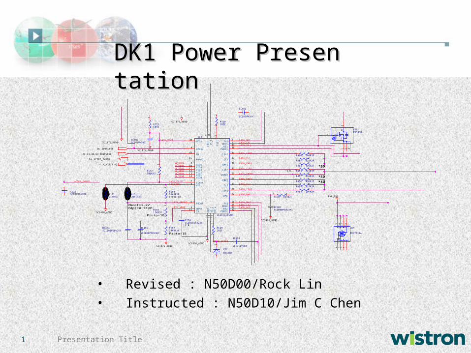
1 Presentation Title
• Revised : N50D00/Rock Lin• Instructed : N50D10/Jim C Chen
PWR_SRC
SC1476_AGND
SC1476_AGND
SC1476_AGND
SC1476_AGND
SC1476_AGND
SC1476_AGND
SC1476_AGND
S.B.
Proto-1B
Vboot=1.2VVdpr=0.749V
S.B.
Proto-1B
Proto-1B
*SD
*SD
*SD
BST2_VCORE
1476_CMP2
1476_LX1
H_VID0
1476_ISH2
H_VID1 1476_CMPRF
1476_DL1
1476_CLSET
1476_PBOOT 1476_DH2
H_VID4
1476_VDRP
1476_CL1
1476_CLRF
1476_VCCA
1476_DAC
H_VID3
1476_HYS 1476_CL2
H_VID5
1476_ISH1
1476_DH1
1476_CMP1
H_VID2
VCORE_PWRGD
1476_DL21476_LX2
BC464SC1000P50V3KX
R150 619R3F1 2
R486 10KR3F1 2
R485 825R3F1 2
R454 10KR3F1 2
BC101SC1000P50V3KX
R152100KR3
12
R1491R3F
12
R5101R3F1
2
U67
SC1476ITSTR
DRN11TG12
BS
T1
3
DPRSL4
VDPR5
PBOOT6
CLSET7
HYS8
VID59
VID410
VID311
VID212
VID113
VID014
SS15
PWRGD16
BS
T2
17
TG218
DRN219
V5_
138
BG137
PGND136
EN35
ISH134
CL133
CMP132
CLRF31
VCCA30
CMPRF29
CMP228
CL227
ISH226
GN
D25
DAC24
CO
RE
23
PGND222BG221
V5_
220
BC465
SC1000P50V3KX
R18161K9R3F
12
BC466
SC1U10V5KX
BC102SC1U10V5KX
BC463
SC1U10V5KX
R15130K1R3F
12
C225SCD1U16V3KX
SSSGD D D D
U69
IRF7811A
12345 6 7 8
D
S
G
U29PH5330
5
4
1 2 3
C224SCD01U16V2KX
R12310R3
12
R483 845R3F1 2
R455 825R3F1 2
R18316K5R3F
12
R18415KR3F
12
R18224K9R3F
12
D49
B0530W
21
R456 499R3F1 2
R484 499R3F1 2
R457 432R3F1 2
DPRSLPVR16
H_VID[5:0]4
RUNPWROK29,33,34,38
VCORE_PWRGD34
DK1DK1 Power Presentation Power Presentation
2 Presentation Title
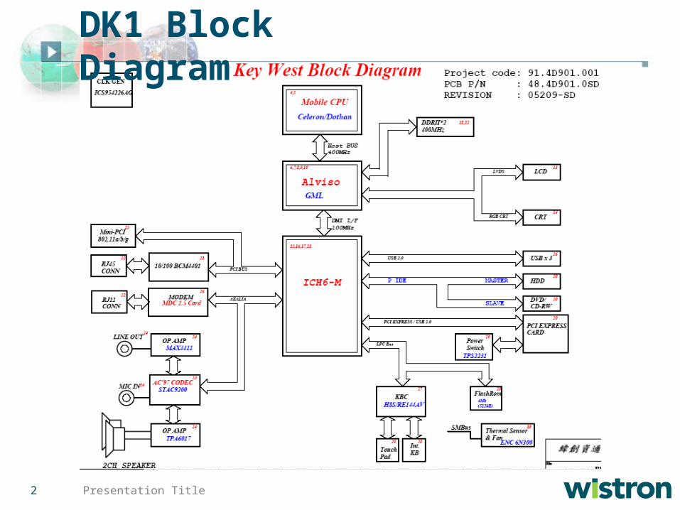
DK1 Block Diagram
3 Presentation Title
Please link to >>>>>> Acrobat ¤å¥ó
Power on sequence block diagram
4 Presentation Title
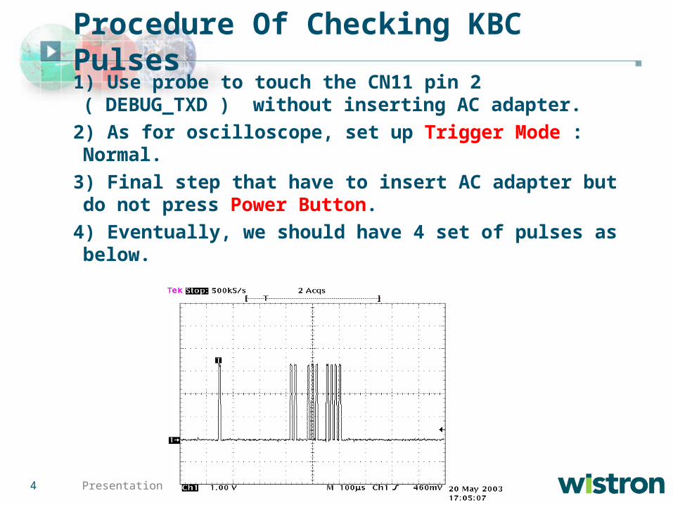
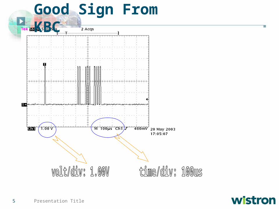
1) Use probe to touch the CN11 pin 2 ( DEBUG_TXD ) without inserting AC adapter.
2) As for oscilloscope, set up Trigger Mode : Normal.
3) Final step that have to insert AC adapter but do not press Power Button.
4) Eventually, we should have 4 set of pulses as below.
Procedure Of Checking KBC Pulses
5 Presentation Title
Good Sign From KBC
6 Presentation Title
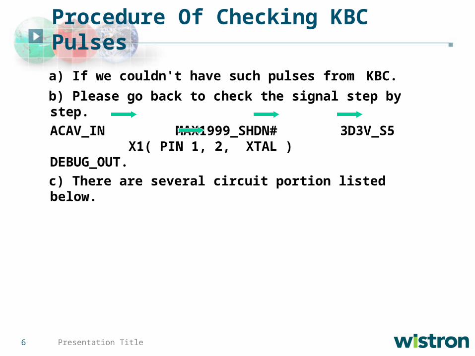
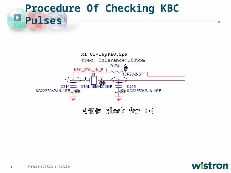
a) If we couldn't have such pulses from KBC.
b) Please go back to check the signal step by step.ACAV_IN MAX1999_SHDN# 3D3V_S5 X1( PIN 1, 2, XTAL ) DEBUG_OUT.
c) There are several circuit portion listed below.
Procedure Of Checking KBC Pulses

7 Presentation Title
Procedure Of Checking KBC Pulses

8 Presentation Title
U55
Procedure Of Checking KBC Pulses
9 Presentation Title
Procedure Of Checking KBC Pulses

10 Presentation Title
Procedure Of Checking KBC Pulses
11 Presentation Title
Procedure Of Checking No Power Issues
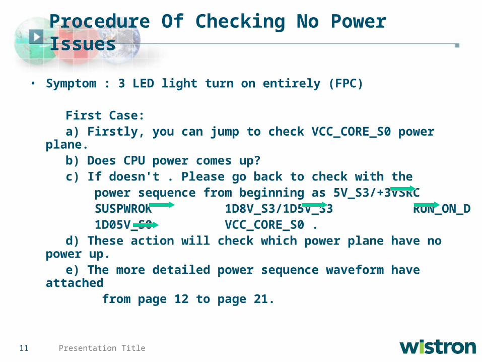
• Symptom : 3 LED light turn on entirely (FPC) First Case: a) Firstly, you can jump to check VCC_CORE_S0 power
plane. b) Does CPU power comes up? c) If doesn't . Please go back to check with the power sequence from beginning as 5V_S3/+3VSRC SUSPWROK 1D8V_S3/1D5V_S3 RUN_ON_D 1D05V_S0 VCC_CORE_S0 . d) These action will check which power plane have no
power up. e) The more detailed power sequence waveform have
attached from page 12 to page 21.

12 Presentation Title
Procedure Of Checking No Power Issues
Second Case:a) Assumed that CPU voltage can attain 0.9 Volt above.b) We may prove that the rest of power plane before
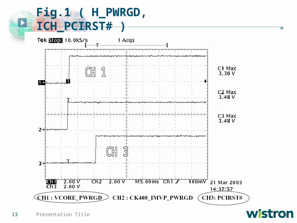
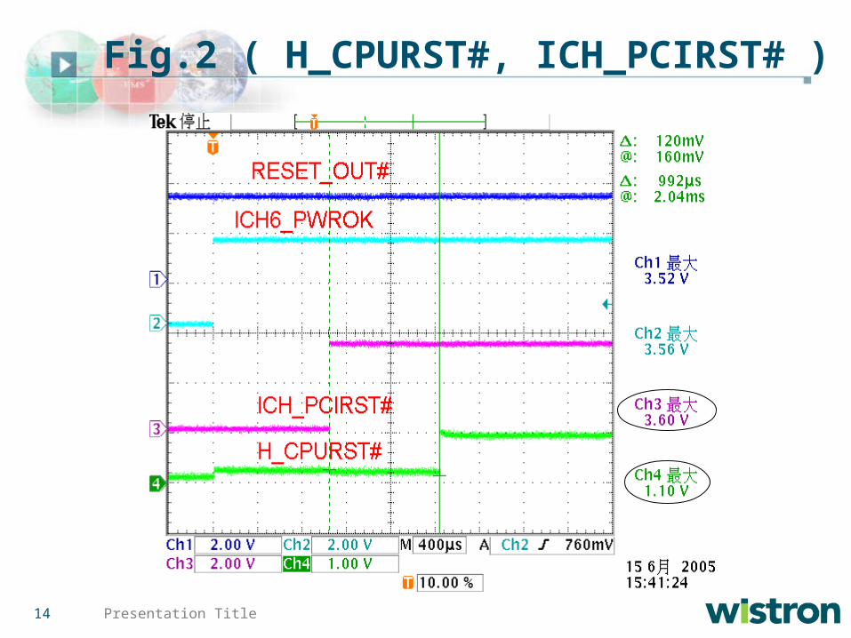
VCC_CORE_S0 power plane would be fine.c) Afterward, please check with ICH_PCIRST#
H_CPURST# . ( See fig.1, fig.2 below )d) If ICH_PCIRST# still can’t exist, we can check the
following signal : RESET_OUT#( From KBC) VRM_PWRGD.
e) If H_CPURST# can’t driven high, the following action should
take is checking the GMCH_PWROK( R431 pin 2 ).f) In addition, we can check whether reference voltage
(2/3 VCCP) for GMCH correct or not, that is, GTLREF, H_VREF.
( R38 pin 1, GTLREF ), ( R311 pin 1, H_VREF ).
13 Presentation Title
Fig.1 ( H_PWRGD, ICH_PCIRST# )
14 Presentation Title
Fig.2 ( H_CPURST#, ICH_PCIRST# )
15 Presentation Title
1) If both H_PWRGD and H_CPURST# driven high as fig.1, fig.2. We’ll keep tracking the next signal which connect between CPU and GMCH, that is, H_ADS#. ( Fig.3 ).
2) We can assume that CPU may failure if we can’t
get these pulses in Fig.3. 3) Another case is only show up one pulse in
Fig.3 that we can suspect the failure in U40
( Bios Rom ).
Procedure Of Checking No Power Issues
16 Presentation Title
18 GTL_ADS# CPU to NB Test pad only .
H_ADS# is the “first signal” generated by CPU ,
Fig.3 ( H_ADS# )
17 Presentation Title
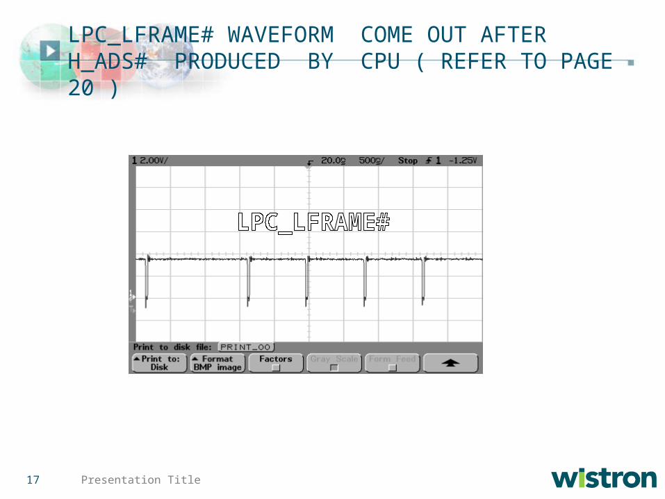
LPC_LFRAME# WAVEFORM COME OUT AFTER H_ADS# PRODUCED BY CPU ( REFER TO PAGE 20 )
18 Presentation Title
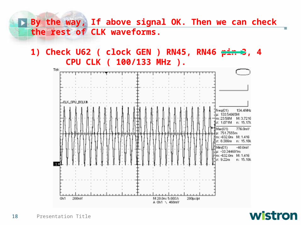
By the way, If above signal OK. Then we can check the rest of CLK waveforms.
1) Check U62 ( clock GEN ) RN45, RN46 pin 3, 4 CPU CLK ( 100/133 MHz ).

19 Presentation Title
2) Check memory CLK ( 200/266 MHz ) which asserts from GMCH. Practically, we can probe the DDR socket ( normal type ) at pin 35, 37.
20 Presentation Title
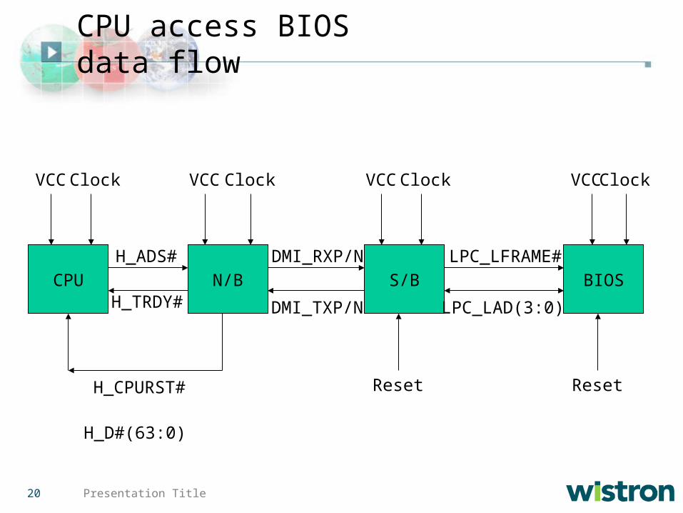
N/B S/B BIOSCPU
VCC VCCVCCVCCClock ClockClockClock
H_CPURST# Reset Reset
H_ADS# DMI_RXP/N LPC_LFRAME#
H_TRDY# DMI_TXP/N
H_D#(63:0)
LPC_LAD(3:0)
CPU access BIOS data flow

21 Presentation Title
DK1 POWER SEQUENCE WAVEFORMTest Purpose: To record the timing sequence for the power rails.
Overview of Procedure: Measure the timing of the power rails. The definition of these timing variables is given in the power sequencing document attached below this table.Timing Variable Time Comments
T01 60.00 us Time of AD+ to DCBATOUT
T02 200.00 us Time of AD+ to ACAV_IN
T03 20.00 us Time of DCBATOUT to +3D3VRTC
T04 31.20 us Time of ACAV_IN to MAX1999_SHDN#
T05 2.18 ms Time of MAX1999_SHDN# to 3D3V_S5
T06 176.00 us Time of MAX1999_SHDN# to 5V_S5
T06-1 32.7ms Time of 3D3V_S5 to EC_RST#
T07 59.20 ms Time of SYS_PWRB# to +3V_SRC
T08 329.00 ms Time of SYS_PWRB# to AUX_EN#
T09 61.20 ms Time of SYS_PWRB# to SUS_ON
T10 380.00 us Time of SUS_ON to 5V_S3
T11 400.00 us Time of SUS_ON to 3VSUS_ON
T12 268.00 ms Time of SUS_ON to +15V
T13 2.58 ms Time of SUS_ON to ICH_RSMRST#
T14 1.40 ms Time of 3VSUS_ON to 3D3V_S3
T15 16.00 us Time of 5V_S3 to +15V
T16 1.51 ms Time of 5V_S3 to SUSPWROK_1999
T17 2.21 ms Time of 5V_S3 to ICH_RSMRST#
T18 820.00 us Time of SUSPWROK_1999 to 1D5V_S3
T19 2.98 ms Time of SUSPWROK_1999 to 1D8V_S3
T20 1.94 ms Time of 1D8V_S3 to DDR_VREF_S3
T21 98.00 ms Time of ICH_RSMRST# to ICH_SLP_S3#
T22 98.40 ms Time of ICH_RSMRST# to RUN_ON
T23 106.00 ms Time of ICH_RSMRST# to RUN_PWROK
T24 1.08 us Time of ICH_SLP_S3# to PM_PWRBTN#
T25 752.00 us Time of ICH_SLP_S3# to 5V_S0
T26 248.00 us Time of ICH_SLP_S3# to 1D5V_S0
T27 2.02 ms Time of ICH_SLP_S3# to RUN_ON_D
T28 400 us Time of RUN_ON_D to 3D3V_S0
T29 576.00 us Time of RUN_ON_D to 2D5V_S0
T30 1.21 ms Time of RUN_ON_D to 1D05V_S0
T31 6.52 ms Time of RUN_ON_D to RUN_PWROK
T32 6.14 ms Time of 3D3V_S0 to RUN_PWROK
T33 1.78 ms Time of RUN_PWROK to VCC_CORE_S0
T34 140.00 us Time of VCC_CORE_S0 to CLK_PWRGD#
T35 4.54 ms Time of VCC_CORE_S0 to VRM_PWRGD
T36 -7.60 ms Time of VCC_CORE_S0 to RESET_OUT#
T37 4.42 ms Time of CLK_PWRGD# to VRM_PWRGD
T38 145.00 ms Time of RESET_OUT# to ICH6_PWROK
T39 1.04 ms Time of ICH6_PWROK to ICH_PCIRST#
T40 992.00 us Time of ICH_PCIRST# to H_CPURST#
Section Owner: Jim C ChenSection Tester: Abel ChangTime To Complete: 06/15
Date Finished: 06/15