1992-8645 adaptive modulation in reconfigurable …
TRANSCRIPT

Journal of Theoretical and Applied Information Technology 10
th October 2014. Vol. 68 No.1
© 2005 - 2014 JATIT & LLS. All rights reserved.
ISSN: 1992-8645 www.jatit.org E-ISSN: 1817-3195
108
ADAPTIVE MODULATION IN RECONFIGURABLE
PLATFORM
1S. SELVAKUMAR,
2Dr.S.RAVI,
3M.VINOTH,
4R.KAMALAKNNAN,
5V.JAYAPRADHA
1345Research scholar, ECE Department, SCSVMV University
2Professor and Head, ECE Department, Dr. M.G.R. Educational and Research Institute University
[email protected],2 [email protected], [email protected], [email protected], [email protected]
ABSTRACT
Autonomous modulation and detection technique in modern communication systems is done using proper
signal detection schemes and prominent receiver structure. The modulation schemes used in this paper are
ASK, FSK, BPSK and QAM. Modulation techniques are created in Simulink which is converted into
Xilinx core and this further undergoes changes using system generator module. This results in the
generation of Verilog files and is deployed in FPGA. Using a microcontroller the FPGA was programmed
with respective bit files and the modulation that had the best channel support is selected. The methodology
used to identify the best modulation for a particular link in reconfiguration is called adaptive modulation
process. The interface is done between the reconfiguring controller (STM32) and the reconfigured FPGA
(XCS250-pq144) using JTAG port. The programmed files were created (XSVF format) and placed in SD-
card of microcontroller. The condition for changing from one modulation to another is based on the link
support and signal position. The HyperTerminal displays the output corresponding to different modulation
selections autonomously. Signal to Noise Ratio (SNR), Available Bandwidth and Bit Error Rate (BER) are
the factors responsible for the selection of modulation scheme. Hence, better quality of service, system
complexity, power efficiency, bandwidth efficiency and cost effectiveness are the advantages of Adaptive
Modulation technique.
Keywords: BER, FPGA, Microcontroller, Modulations, SNR, and Xilinx.
1. INTRODUCTION
In order to transmit communication
signals, some modification has to be done and this
conversion process is called modulation. During
modulation the base band signal is used to modify
some parameter of a high frequency carrier signal.
This is achieved by varying any one of the
parameters, such as amplitude, frequency or phase
of the carrier which is a sinusoid of high frequency,
in proportion to the base band signal. Dependent on
the constraint being various we have amplitude
modulation, and frequency modulation or phase
modulation. [1]
Digital modulation for analog carrier
signal is modulated by a numeral bit stream of
either equivalent length signals or variable size
signals. This can be labeled as a form of analog to
digital variation. The variations in the carrier signal
are selected from a predetermined number of other
symbols. These are the most important digital
modulation techniques [2] [5]. The most important
digital modulation procedures namely PSK, FSK,
and ASK uses finite number of phases, frequencies,
amplitudes respectively. Another basic digital
modulation technique called QAM uses a finite
number of at the least 2 phases and 2 amplitudes.
Fixed number of amplitudes receiving QAM can be
seen as a two channel structure. The resultant is a
mixture of PSK and ASK, which uses a limited
number of at the least two phases and a limited
number of at the least two amplitudes. Every
phases, frequency or amplitude is allocated to a
distinctive pattern of binary bits. Generally, each of
these phases, frequencies or amplitudes codes a
same number of bits. This same number of bits
contains the symbol which is characterized by the
specific phase. [3]
Figure 1: Constellation diagram
The Figure 1 constellation diagram
represents the modulation techniques PSK, ASK,
Journal of Theoretical and Applied Information Technology 10
th October 2014. Vol. 68 No.1
© 2005 - 2014 JATIT & LLS. All rights reserved.
ISSN: 1992-8645 www.jatit.org E-ISSN: 1817-3195
109
and QAM appropriately as modulation alphabets,
where the x-axis represents the amplitudes of I
signal and y-axis represents the amplitude of the Q
signal for every symbol. Mostly PSK and ASK, and
rarely FSK can be produced and detected with the
help of principle of QAM. I and Q signal joins
together to form a very complex valued signal
termed as equivalent low pass. This illustrates the
clear picture of valued modulated physical signal,
sometimes also named as pass band signal or RF
signal. [5]
2. NEED FOR ADAPTIVE MODULATION:
Adaptive modulation systems invariably
require some channel state information at the
transceiver. This could be developed in Time
division duplex systems by assuming that the
transmission of the channel between the transmitter
and the receiver is nearly equal to the channel
between the transmitter and the receiver. On the
other hand, the channel data can also be directly
measured at the headphones, and fed back to the
source. Adaptive modulation systems increase rate
of transmission, and improve the bit error rates by
exploiting the channel state data that is present at
the transmitter. Adaptive modulation a system
shows excellent performance enhancements when
compared to the systems which do not uses channel
information at the transmitter. [5][8]
Adaptive modulation technique is done especially
by changing the modulation scheme usage to its
existing channel state to increase the achieved data
rate. Since Adaptive modulation techniques’
excellences in mobile scenarios are very high, the
studies of the technique have been widely taking
place in mobile scenarios. Also, the excellence of
the technique in mobile radio communication
happens in connection with the conventional
modulation strategies. Due to that statistic,
adaptive modulation techniques execution is best
suited for cognitive radios and SDRs.
Subsequently, the essential core of those radios
works based on software, thus associate adaptive
modulation techniques will have changing pattern.
Also, the existing capacity of adaptive modulation
techniques uses wireless communication links to
bring in a notable impact to the transmission
security. [9]
Adaptive modulation varies modulation
parameters that are related to channel fading and
improves the performance, varying modulation and
coding that are related to fading. Adaptive
modulation Parameters are Constellation size,
Transmit power, Instantaneous BER, Symbol time
and coding rate/scheme. The Optimization
criterions for adaptive modulation are Maximize
throughput, Minimize average power and Minimize
average BER. [10]
3. ADAPTIVE MODULATION IN
RECONFIGURABLE HARDWARE
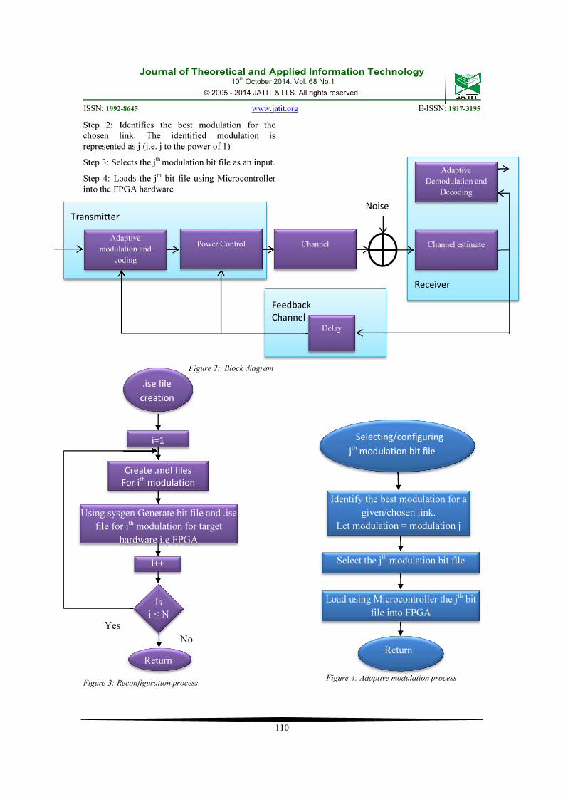
Adaptive modulation reconfigurable process
block diagram is shown in Figure 2. Transmitter
sections have adaptive modulation coding and
power control. Receiver sections have Adaptive
demodulation coding and channel estimation. Delay
section gives the channel feedback to the
transmitter. [9]
Using a microcontroller the FPGA was
programmed with respective bit files (configuration
bits) and the modulation that had the best channel
support is selected. The methodology is used to
identify the best modulation for a particular link.
The reconfiguration process is illustrated in the
flow chart as in Figure 3. [13].
Reconfiguration process steps are:
Step 1: ISE files are created by Xilinx core for
each modulation schemes.
Step 2: The first created modulation scheme is
represented as i=1.
Step 3: Modulation selection creates the .mdl file
for ith
modulation.
Step 4: Using system generation, generated bit file
and .ise file for ith
modulation are made target for
the FPGA hardware.
Step 5: In the next step, the value of “i” is
incremented by 1.
Step 6: This is followed by a condition i<=N, and
if the i value passes the condition it goes back to
Step 2 and I value is taken as i = 2.
The above process continues till the input is
stopped.
Adaptive modulation process is shown in
figure 4. The Adaptive modulation process helps to
select and load the required modulation programs
into the FPGA hardware.
The steps involved in Adaptive modulation process
are:
Step 1: Lists the available modulation schemes. All
of these modulation files are represented as jth
modulation bit file.
Journal of Theoretical and Applied Information Technology 10
th October 2014. Vol. 68 No.1
© 2005 - 2014 JATIT & LLS. All rights reserved.
ISSN: 1992-8645 www.jatit.org E-ISSN: 1817-3195
110
Step 2: Identifies the best modulation for the
chosen link. The identified modulation is
represented as j (i.e. j to the power of 1)
Step 3: Selects the jth
modulation bit file as an input.
Step 4: Loads the jth
bit file using Microcontroller
into the FPGA hardware
Figure 2: Block diagram
Figure 3: Reconfiguration process
Figure 4: Adaptive modulation process
Yes
Return
i++
Is
i ≤ N
No
Using sysgen Generate bit file and .ise
file for ith modulation for target
hardware i.e FPGA
i=1
Create .mdl files
For ith
modulation
.ise file
creation
Select the jth modulation bit file
Load using Microcontroller the jth bit
file into FPGA
Identify the best modulation for a
given/chosen link.
Let modulation = modulation j
Selecting/configuring
jth
modulation bit file
Return
Receiver
Transmitter
Channel estimate
Adaptive
Demodulation and
Decoding
Feedback
Channel
Delay
Adaptive
modulation and
coding
Power Control Channel
Noise

Journal of Theoretical and Applied Information Technology 10
th October 2014. Vol. 68 No.1
© 2005 - 2014 JATIT & LLS. All rights reserved.
ISSN: 1992-8645 www.jatit.org E-ISSN: 1817-3195
111
4. HARDWARE IMPLEMENTATION
Individual modulation schemes were built as
.mdl files in Simulink with Xilinx core and using
system generator module, the Verilog files were
generated and deployed in FPGA. Figure 5 to
Figure 10 shows the Xilinx blocks generated for
types of modulation schemes namely ASK, FSK,
BPSK. Similar Xilinx cores for other modulation
schemes were also built, generated and deployed in
FPGA [18] [19].
4.1 Case (i) ASK
Figure 5: ASK Module built in xilinx-sysgen core
Figure 6: ASK output Simulated for Random Data
4.2 Case (ii) FSK
Figure 7: FSK Module built in Xilinx- sysgen core
Figure 8: FSK output Simulated for Random Data
4.3 Case (iii) BPSK
Figure 9: BPSK Module built in Xilinx - sysgen core
Figure 10: BPSK output Simulated for Random Data
QAM representation of system generator module is
shown in Figure 11. Figure 12 displays a Simulink
model with the QAM system design, together with
the channel typical, transmitter, and the receiver.
The Forward Error Correction, QAM Receiver

Journal of Theoretical and Applied Information Technology 10
th October 2014. Vol. 68 No.1
© 2005 - 2014 JATIT & LLS. All rights reserved.
ISSN: 1992-8645 www.jatit.org E-ISSN: 1817-3195
112
subsystems and QAM Symbol Mapping have been
modeled using receiver sections and transmitter.
This kind of approach provides a logical group of
functionality, clean top-level representation, and a
framework for execution and verification of the
design sections. Figure 11 displays the contents of
the transmitter subsystem that develops a stream of
8-bit symbols produced by a sinusoidal test basis in
the superior model. [15]
Figure 11: Qam Transmitter
In channel modeling the data that is modulated is
delivered through a channel model. This model
simulates the effects of inter symbol interference,
additive white Gaussian noise, and Doppler shifting
using the Simulink blocks. The model uses a bar
that can slide over to change the Doppler shift
while the simulation works to check the receiver’s
robustness. [15][18]
Figure 12: Qam Receiver
Figure 12 shows the QAM Receiver subsystem. As
our design is intended for an FPGA, it includes
blocks from the System Generator Block set. The
QAM Demodulator subsystem accomplishes QAM
demodulation (carrier recovery, adaptive
equalization, and slicing), and the rest of the
receiver accomplishes frame alignment and RS and
Viterbi decoding. This also contains a switch to
decide QAM phase ambiguity. [19]
5. IMPLEMENTATION AND RESULTS:
The hardware consisting of microcontroller
(for reconfiguring the FPGA), FPGA board and the
DAC for interface to the audio port is .shown in
Figure 13. The microcontroller autonomously
programs the modulation selection block in Xilinx
core placed in FPGA. The criteria for changing
from an existing modulation to a newer one are
based on the link support and signal condition.[18]
Figure13: Hardware Units With FPGA, Microcontroller
And DAC
The HyperTerminal display output
corresponding to three different modulation
selections is shown in Figure 14 to Figure 16
Figure 14: Hyperterminal ASK Display Output

Journal of Theoretical and Applied Information Technology 10
th October 2014. Vol. 68 No.1
© 2005 - 2014 JATIT & LLS. All rights reserved.
ISSN: 1992-8645 www.jatit.org E-ISSN: 1817-3195
113
Figure 15: Hyperterminal BPSK Display Output
Figure 16: Hyperterminal FSK Display Output
4. CONCLUSION
Xilinx code together with System
generator produces a code in which synthesis
becomes very easy. Thereby, the test vectors and
test bench generates in an excellent way for
verification. The existing system does not have
reusability properties. Adaptive Modulation in
Reconfigurable Platform is designed and
implemented in hardware to overcome this
limitation. Using a microcontroller the FPGA was
programmed with particular bit files and the
modulation that had the best channel provision is
selected. The condition for changing from one
modulation to another is based on the link support
and signal position. The HyperTerminal displays
the output corresponding to different modulation
select independently. This further allows the
assembly of high efficient designs of FPGA.
Xilinx system generator tool cannot take
data which is multi-dimensional; this is one of its
limitations. Therefore, the standard condition has to
be restricted. This incapability leads to an extra step
wherein the designer should feed data as one-
dimension data. Also, functions that works using
multi-dimension feeds has to be changed. Although
Xilinx system generators is considered to be a real
advanced design tool since it has created an
impression that Xilinx system generators manages
even small details by itself, it is not completely
justified when the operator connects it with higher
level blocks[15]. The tool needs manual effort of
the designer in all the aspects like timing, controls
and delays other than the usual execution processes
of the design flow. In Future, the work will be
focused on overcoming the limitations and
further direction of study shall be focused on
optimizing network layer routing [16] [17].
REFRENCES:
[1] A.H. Bastami, and A. Olfat, “Selection Relaying
Schemes for Cooperative Wireless Networks
With Adaptive Modulation”, IEEE Transactions
on Vehicular Technology, Volume: 60, Issue: 4
May 2011. Page(s):1539 - 1558
[2] Md.J. Hossain, P.K Vitthaladevuni, A.J.
Goldsmith, V.K Bhargava, and M.S Alouini,
“Adaptive hierarchical modulation for
simultaneous voice and multiclass data
transmission over fading channels” IEEE
Transactions on Vehicular
Technology, Volume: 55, 2006 Page(s): 1181 -
1194

Journal of Theoretical and Applied Information Technology 10
th October 2014. Vol. 68 No.1
© 2005 - 2014 JATIT & LLS. All rights reserved.
ISSN: 1992-8645 www.jatit.org E-ISSN: 1817-3195
114
[3] B. Schrenk, P. Bakopoulos, E. Kehayas, A.
Maziotis, J.A Lazaro, H. Avramopoulos, and
Prat.J. “An All-Optical Carrier Recovery
Scheme for Access Networks with
Simple ASK Modulation”, IEEE Journal
of Optical Communications and Networking,
Volume: 3, Issue: 9, 2011.
[4] M.S Alouini F.F, and Digham, “Adaptive M-
FSK modulation for power limited systems”
Vehicular Technology Conference, IEEE
56th Volume: 2, 2002
[5] A. Svensson, “An Introduction
to Adaptive QAM Modulation Schemes for
Known and Predicted Channels” Proceedings of
the IEEE Volume: 95, Issue: 12, 2007
[6] Alexandra Duel-Hallen, and Tao Jia, “Adaptive
Bit-Interleaved Coded Modulation Based on the
Expurgated Bound for Mobile Radio OFDM
Systems Aided by Fading Prediction”, IEEE
transactions on communications, volume 60,
august 2012
[7] Mohammad Torabi, Jean François Frigon, and
BrunildeSanso, “Performance Analysis of
Adaptive Modulation in Multiuser Selection
Diversity Systems with OSTBC over Time
Varying Channels”, Signal processing letters,
IEEE volume 19, April 2012
[8] Tao Jia, Hans Hallen, and Alexandra Duel-
Hallen, “Data-Aided Noise Reduction for Long
Range Fading Prediction in Adaptive
Modulation Systems”, vehicular technology,
IEEE transactions on volume 62, Issue. 5, June
2013.
[9] Mohamed-Slim Alouini, and Anlei Rao,
“Multiuser Diversity with Adaptive Modulation
in Non-Identically Distributed Nakagami
Fading Environments”, IEEE transactions on
vehicular technology, volume 61, no. 3, march
2012
[10] T. Foukal as a George, B. Karetsos, “On the
performance of adaptive modulation in
cognitive radio Networks”, Elsevier publication
2013
[11] James Gross a Marc Emmelmannb, B.C Adam
Wolisz, and, A. Oscar Puñal, “Enhancing IEEE
802.11a/n with dynamic single-user OFDM
adaptation”, Elsevier publication 2008
[12] Zlatka Nikolova, Vladimir Poulkov, Georgi
Iliev and Karen Egiazarian, “New adaptive
complex IIR filters and their application in
OFDM systems”, Springer-Verlag London
Limited 2009.
[13] Wei Xing Zheng, and Jinhui Zhang,
“Design of Adaptive Sliding Mode Controllers
for Linear Systems via Output Feedback”, IEEE
Transaction on Industrial Electronics, Volume:
61 , Issue: 7 Publication Year: 2014 , Page(s):
3553 – 3562
[14] R. Faraji, A. Rouholamini, H. RNaji, R.
Fadaeinedjad, and M.R.Chavoshian “FPGA-
based real time incremental conductance
maximum power point tracking controller for
photovoltaic systems” Power Electronics,
IET Volume: 7 , Issue: 5 Publication Year:
2014 , Page(s): 1294 – 1304
[15] S. Kompella, Y.T. Shiwen Mao, H.D. Sherali,
“Cross-layer optimized multipath routing for
video communications in wireless networks”
Selected Areas in Communications, IEEE
Journal on (Volume: 25, Issue: 4) May 2007
Page(s): 831 - 840
[16] M. Cheng, Quanmin Ye, Lin CaI “Cross-Layer
Schemes for Reducing Delay in Multihop
Wireless Networks” Wireless Communications,
IEEE Transactions on (Volume:12 , Issue: 2 )
February 2013 Page(s): 928 – 937
[17] R. Woods, J. McAllister, G. Lightbody and Y.
Li, “FPGA based Implementation of Signal
Processing Systems,” A John Wiley & Sons Inc,
publication, 2008
[18] Xilinx System Generator for DSP User Guide,
r10.1.1, April 2008.
[19] Digilent Spartan-3E Starter Board with Xilinx
XC3S500EFPGA
(http://digilentinc.com/Products/Detail.cfm?Nav
Path=2,400,792&Prod=S3EBOARD)