(19) tzz z t - patentimages.storage.googleapis.com · ratus according to the fourth embodiment;...
TRANSCRIPT

Note: Within nine months of the publication of the mention of the grant of the European patent in the European PatentBulletin, any person may give notice to the European Patent Office of opposition to that patent, in accordance with theImplementing Regulations. Notice of opposition shall not be deemed to have been filed until the opposition fee has beenpaid. (Art. 99(1) European Patent Convention).
Printed by Jouve, 75001 PARIS (FR)
(19)E
P2
081
256
B1
TEPZZ Z8_ 56B_T(11) EP 2 081 256 B1
(12) EUROPEAN PATENT SPECIFICATION
(45) Date of publication and mention of the grant of the patent: 25.03.2015 Bulletin 2015/13
(21) Application number: 07806066.2
(22) Date of filing: 24.08.2007
(51) Int Cl.:H01Q 1/00 (2006.01) H01Q 5/00 (2015.01)
H01Q 9/04 (2006.01) H01Q 9/40 (2006.01)
H01Q 9/46 (2006.01) H01Q 21/20 (2006.01)
(86) International application number: PCT/JP2007/066480
(87) International publication number: WO 2008/023800 (28.02.2008 Gazette 2008/09)
(54) ANTENNA DEVICE
ANTENNENVORRICHTUNG
DISPOSITIF D’ANTENNE
(84) Designated Contracting States: AT BE BG CH CY CZ DE DK EE ES FI FR GB GR HU IE IS IT LI LT LU LV MC MT NL PL PT RO SE SI SK TR
(30) Priority: 24.08.2006 JP 200622819708.02.2007 JP 2007029438
(43) Date of publication of application: 22.07.2009 Bulletin 2009/30
(73) Proprietor: Hitachi Kokusai Yagi Solutions Inc.Kodaira-shi,Tokyo187-8512 (JP)
(72) Inventors: • FUJITA, Seiken
Tokyo 187-8511 (JP)• NAKANO, Hisamatsu
Tokyo 187-0021 (JP)
• WAKO, IichiTokyo 187-8511 (JP)
• TANAKA, KenTokyo 187-8511 (JP)
• UMEGAKI, ToshihitoTokyo 187-8511 (JP)
(74) Representative: Günther, Constantin et alGramm, Lins & Partner Freundallee 13 a30173 Hannover (DE)
(56) References cited: JP-A- 07 303 005 JP-A- 10 126 149JP-A- 10 276 032 JP-A- 11 205 036JP-A- 2000 077 923 JP-A- 2003 101 341JP-A- 2003 142 935 JP-A- 2003 338 783JP-A- 2004 072 731 JP-A- 2004 072 731JP-A- 2005 020 289 JP-A- 2005 020 289US-A- 5 784 032 US-A- 5 926 150

EP 2 081 256 B1
2
5
10
15
20
25
30
35
40
45
50
55
Description
Technical Field
[0001] The present invention relates to an antenna ap-paratus used in a relay unit.
Background Art
[0002] As an antenna for relay which re-transmitsground wave for a mobile phone, television broadcast,or the like to a blind zone such as an underground mall,a small-sized and weight-reduced antenna is demandedin view of a problem about an installation place, aestheticpurposes or the like. As an antenna for relay, verticalpolarized and horizontal-plane nondirectional antenna isfrequently used.[0003] As a known technique relating to the presentinvention, a bidirectional polarized antenna apparatuswhich is provided with a bidirectional antenna for hori-zontal polarization having a plurality of linear radiatingelement portions configured to excite a linear or planarimpedance matching element portion according to one-point power feeding from a back thereof and providedperpendicularly to the matching element portion, a plu-rality of distal ends of the linear radiating element portionsbeing grounded, and a grounding plate, where the bidi-rectional antenna for horizontal polarization is disposedon the grounding plate is known (see, Jpn. Pat. Appl.KOKAI Publication No. 11-205036).[0004] A compact broadband antenna derived from theinverted-F antenna configuration is disclosed in U.S.5,926,150. The tapered inverted-F antenna is able togenerate high intensity electric fields with a physicallysmall package size.[0005] A compact diversity antenna is disclosed in US5,784,032.
Disclosure of Invention
[0006] Since a relay antenna installed in an under-ground mall or the like is generally provided on a ceilingor the like, it is required to be small-sized and be reducedin profile (a total height is low).[0007] However, since the above mentioned conven-tional monopole antenna must have a height of at leastabout1/4 wavelength and it is difficult to achieve furtherlow profile, it is undesirable as a relay antenna Installedin an underground mall or the like. A monopole antennacan obtain excellent characteristics in a single frequencyband, but it basically corresponds to a narrow band andits specific bandwidth in a region where VSRW (voltagestanding wave ratio) is low, for example, 2 or less is gen-erally about ten and several percentages, so that it isdifficult to apply the monopole antenna to an apparatuswhich performs bulk transmission according to a wide-band communication.[0008] The present invention has been made to solve
the above mentioned problem and an object thereof isto provide an antenna apparatus which realizes size re-duction and low profile, and wider band. This object isachieved by an antenna apparatus as specified in claims1.[0009] According to a first aspect of the present, thereis provided an antenna apparatus comprising: a conduc-tor plate; a radiating element arranged to face the con-ductor plate and partially short-circuited to the conductorplate; a feeding terminal provided on the conductor plate;and a feeding path connecting the feeding terminal anda feeding portion of the radiating element to each other.Furthermore, the antenna apparatus according to the firstaspect further includes at least one passive element ca-pacitance-coupled to a line path connecting the short-circuiting portion of the radiating element and the feedingpath to each other.[0010] According to a second aspect of the present,there is provided an antenna apparatus comprising: aconductor plate; a radiating element arranged to face theconductor plate and partially short-circuited to the con-ductor plate; a feeding terminal provided on the conduc-tor plate; and a feeding path connecting the feeding ter-minal and a feeding portion of the radiating element toeach other, wherein the feeding path has such a shapethat a width thereof is expanded from the side of the feed-ing terminal toward the side of the feeding portion.[0011] According to a third aspect of the present, thereis provided an antenna apparatus comprising: a conduc-tor plate; a radiating element arranged to face the con-ductor plate and partially short-circuited to the conductorplate; a feeding terminal provided at a central portion ofthe conductor plate; and a feeding path whose one endis connected to the feeding terminal and whose other endis capacitance-coupled to a feeding portion of the radi-ating element, wherein the feeding path has such a shapethat a width thereof is expanded from the side of the feed-ing terminal toward the side of the feeding portion. Fur-thermore, according to the third aspect of the antennaapparatus, the other end is partially connected to thefeeding portion.[0012] Furthermore, each aspect of the above has thefollowing characteristics.[0013] The radiating element comprises a plurality ofline paths expanding about the feeding portion radiallyat equal intervals and the line paths are short-circuitedto the conductor plate, respectively.[0014] The radiating element further includes linepaths connecting end portions of adjacent line paths ofthe plurality of line paths.[0015] The conductor plate further includes a matchingportion near the short-circuiting portion of the radiatingelement.[0016] The short-circuiting portions of the radiating el-ement are provided on the circumference of a circle aboutthe feeding path at equal intervals.[0017] The radiating element is defined as a first radi-ating element and a second radiating element having a
1 2

EP 2 081 256 B1
3
5
10
15
20
25
30
35
40
45
50
55
facing distance between the conductor plate and the sec-ond radiating element shorter than a facing distance be-tween the conductor plate and the first radiating elementis further disposed between the conductor plate and thefirst radiating element.
Brief Description of Drawings
[0018]
FIG. 1 is a perspective view showing a basic config-uration of an antenna apparatus according to a firstembodiment of the present invention;FIG. 2 is a side view of the antenna apparatus ac-cording to the first embodiment;FIG. 3A is a perspective view showing a configura-tion of an antenna apparatus according to a secondembodiment of the present invention;FIG. 3B is a perspective view showing an arrange-ment configuration of a passive element portion ofthe antenna apparatus;FIG. 4 is a side view of the antenna apparatus ac-cording to the second embodiment;FIG. 5 is a real part impedance characteristic dia-gram of the antenna apparatus according to the sec-ond embodiment;FIG. 6 is an imaginary part impedance characteristicdiagram of the antenna apparatus according to thesecond embodiment;FIG. 7 is a perspective view of an antenna apparatuswhere a passive element is not provided;FIG. 8 is an impedance characteristic diagram of theantenna apparatus shown in FIG. 7;FIG. 9 is a VSWR characteristic diagram of the an-tenna apparatus shown in FIG. 7;FIG. 10 is a perspective view of an antenna appara-tus where a passive element is provided;FIG. 11 is an impedance characteristic diagram ofthe antenna apparatus shown in FIG. 10;FIG. 12 is a VSWR characteristic diagram of the an-tenna apparatus shown in FIG. 10;FIG. 13 is a perspective view showing a configurationof an antenna apparatus according to a third embod-iment of the present invention;FIG. 14 is a diagram showing an equivalent circuitof the antenna apparatus shown in FIG. 13;FIG. 15 is a real part impedance characteristic dia-gram of the antenna apparatus according to the thirdembodiment;FIG. 16 an imaginary part impedance characteristicdiagram of the antenna apparatus according to thethird embodiment;FIG. 17 is a VSWR characteristic diagram of the an-tenna apparatus according to the third embodiment;FIG. 18 is a real part impedance characteristic dia-gram when a passive element is not provided in theantenna apparatus according to the third embodi-ment;
FIG. 19 is an imaginary part impedance character-istic diagram when a passive element is not providedin the antenna apparatus according to the third em-bodiment;FIG. 20 is a VSWR characteristic diagram when apassive element is not provided in the antenna ap-paratus according to the third embodiment;FIG. 21 is a perspective view of an antenna appara-tus having a disk-like antenna element;FIG. 22 is a real part impedance characteristic dia-gram of the antenna apparatus shown in FIG. 21;FIG. 23 is an imaginary part impedance character-istic diagram of the antenna apparatus shown in FIG.21;FIG. 24 is a VSWR characteristic diagram of the an-tenna apparatus shown in FIG. 21;FIG. 25 is a perspective view showing a configurationof an antenna apparatus according to a fourth em-bodiment of the present invention;FIG. 26 is a VSWR characteristic diagram when amatching plate is not provided in the antenna appa-ratus according to the fourth embodiment;FIG. 27 is a VSWR characteristic diagram of the an-tenna apparatus according to the fourth embodi-ment;FIG. 28 is a diagram showing a vertically-polarizedhorizontal plane directionality of the antenna appa-ratus according to the fourth embodiment at a fre-quency of 470 MHz;FIG. 29 is a diagram showing a vertically-polarizedhorizontal plane directionality of the antenna appa-ratus according to the fourth embodiment at a fre-quency of 590 MHz;FIG. 30 is a diagram showing a vertically-polarizedhorizontal plane directionality of the antenna appa-ratus according to the fourth embodiment at a fre-quency of 710 MHz;FIG. 31 is a diagram showing a vertically-polarizedvertical plane directionality of the antenna apparatusaccording to the fourth embodiment at a frequencyof 470 MHz;FIG. 32 is a diagram showing a vertically-polarizedvertical plane directionality of the antenna apparatusaccording to the fourth embodiment at a frequencyof 590 MHz;FIG. 33 is a diagram showing a vertically-polarizedvertical plane directionality of the antenna apparatusaccording to the fourth embodiment at a frequencyof 710 MHz;FIG. 34 is a perspective view showing a configurationof an antenna apparatus according to a fifth embod-iment which is not covered by the present invention;FIG. 35 is a perspective view showing a configurationof an antenna apparatus according to a sixth em-bodiment of the present invention;FIG. 36 is a side view showing details of a feedingpath portion in the sixth embodiment;FIG. 37 is a real part impedance characteristic dia-
3 4

EP 2 081 256 B1
4
5
10
15
20
25
30
35
40
45
50
55
gram in a feeding portion of the antenna apparatusaccording to the sixth embodiment;FIG. 38 is an imaginary part impedance character-istic diagram of the antenna apparatus according tothe sixth embodiment;FIG. 39 is a VSWR characteristic diagram of the an-tenna apparatus according to the sixth embodiment;FIG. 40 is a diagram showing vertically-polarizedhorizontal plane directionality (X-Y plane) of the an-tenna apparatus according to the sixth embodimentat a frequency of 500 MHz;FIG. 41 is a diagram showing vertically-polarizedhorizontal plane directionality (X-Y plane) of the an-tenna apparatus according to the sixth embodimentat a frequency of 1 GHz;FIG. 42 is a diagram showing vertically-polarizedhorizontal plane directionality (X-Y plane) of the an-tenna apparatus according to the sixth embodimentat a frequency of 1.6 GHz;FIG. 43 is a side view showing details of a feedingpath portion of an antenna apparatus according to aseventh embodiment of the present invention;FIG. 44 is a VSWR characteristic diagram of the an-tenna apparatus according to the seventh embodi-ment;FIG. 45A is a perspective view showing another con-figuration example of a feeding path in the seventhembodiment;FIG. 45B is a side view showing another configura-tion example of a feeding path in the seventh em-bodiment;FIG. 46 is a perspective view showing a configurationof an antenna apparatus according to an eighth em-bodiment of the present invention;FIG. 47 is a perspective view showing details of afeeding path portion in the eighth embodiment;FIG. 48 is a perspective view showing a configurationof an antenna apparatus according to a ninth em-bodiment of the present invention;FIG. 49 is a perspective view showing a configurationof an antenna apparatus according to a tenth em-bodiment of the present invention;FIG. 50 is a perspective view showing a configurationof an antenna apparatus according to an eleventhembodiment of the present invention;FIG. 51 is a perspective view showing a configurationof an antenna apparatus according to a twelfth em-bodiment of the present invention;FIG. 52 is a VSWR characteristic diagram when alength of a radiating element is made long and anoperation frequency is set to be low;FIG. 53A is a perspective view showing a configu-ration example of a short-circuiting element in an an-tenna apparatus according to a thirteenth embodi-ment of the present invention;FIG. 53B is a perspective view showing another con-figuration example of the short-circuiting element inthe antenna apparatus according to the thirteenth
embodiment;FIG. 54 is a VSWR characteristic diagram of the an-tenna apparatus according to the thirteenth embod-iment;FIG. 55 is a perspective view showing a configurationexample of an antenna apparatus according to a six-teenth embodiment of the present invention;FIG. 56 is a plan view of a radiating element of theantenna apparatus according to the sixteenth em-bodiment;FIG. 57 is a side view of the antenna apparatus ac-cording to the sixteenth embodiment;FIG. 58 is a real part impedance characteristic dia-gram when the radiating element and a feeding pathare directly connected to each other in the antennaapparatus according to the sixteenth embodiment;FIG. 59 is an imaginary part impedance character-istic diagram when the radiating element and thefeeding path are directly connected to each other inthe antenna apparatus according to the sixteenthembodiment;FIG. 60 is a VSWR characteristic diagram when theradiating element and the feeding path are directlyconnected to each other in the antenna apparatusaccording to the sixteenth embodiment;FIG. 61 is areal part impedance characteristic dia-gram of the antenna apparatus according to the six-teenth embodiment;FIG. 62 is an imaginary part impedance character-istic diagram of the antenna apparatus according tothe sixteenth embodiment;FIG. 63 is a VSWR characteristic diagram of the an-tenna apparatus according to the sixteenth embod-iment;FIG. 64 is a perspective view showing a configurationof an antenna apparatus according to a fifteenth em-bodiment of the present invention;FIG. 65 is a real part impedance characteristic dia-gram when a conductor plate is set to 410 mm anddirect connection is performed in the antenna appa-ratus according to the fourteenth embodiment;FIG. 66 is an imaginary part impedance character-istic diagram when the conductor plate is set to 410mm and direct connection is performed in the anten-na apparatus according to the fourteenth embodi-ment;FIG. 67 is a VSWR characteristic diagram when theconductor plate is set to 410 mm and direct connec-tion is performed in the antenna apparatus accordingto the fourteenth embodiment;FIG. 68 is a real part impedance characteristic dia-gram when the conductor plate is set to 410 mm andcapacitance coupling is performed in the antennaapparatus according to the fourteenth embodiment;FIG. 69 is an imaginary part impedance character-istic diagram when the conductor plate is set to 410mm and capacitance coupling is performed in theantenna apparatus according to the fourteenth em-
5 6

EP 2 081 256 B1
5
5
10
15
20
25
30
35
40
45
50
55
bodiment;FIG. 70 is a VSWR characteristic diagram when theconductor plate is set to 410 mm and capacitancecoupling is performed in the antenna apparatus ac-cording to the fourteenth embodiment;FIG. 71 is a real part impedance characteristic dia-gram when direct connection is performed in an an-tenna apparatus according to a fifteenth embodi-ment;FIG. 72 is an imaginary part impedance character-istic diagram when direct connection is performed inthe antenna apparatus according to the fifteenth em-bodiment;FIG. 73 is a VSWR characteristic diagram when di-rect connection is performed in the antenna appara-tus according to the fifteenth embodiment;FIG. 74 is a real part impedance characteristic dia-gram when capacitance coupling is performed in theantenna apparatus according to the fifteenth embod-iment;FIG. 75 is an imaginary part impedance character-istic diagram when capacitance coupling is per-formed in the antenna apparatus according to thefifteenth embodiment;FIG. 76 is a VSWR characteristic diagram when ca-pacitance coupling is performed in the antenna ap-paratus according to the fifteenth embodiment;FIG. 77 is a perspective view showing a configurationof an antenna apparatus according to a sixteenthembodiment of the present invention;FIG. 78 is a side view of the antenna apparatus ac-cording to the sixteenth embodiment;FIG. 79 is a VSWR characteristic diagram of the an-tenna apparatus according to the sixteenth embod-iment;FIG. 80 is a diagram showing vertically-polarizedhorizontal plane directionality (coordinate axis e =45° X - Y plane in FIG. 17) of the antenna apparatusaccording to the sixteenth embodiment of thepresent invention at a frequency of 0.7 GHz;FIG. 81 is a diagram showing vertically-polarizedhorizontal plane directionality (coordinate axis θ =45° X - Y plane in FIG. 17) of the antenna apparatusaccording to the sixteenth embodiment of thepresent invention at a frequency of 1.7 GHz;FIG. 82 is a diagram showing vertically-polarizedhorizontal plane directionality (coordinate axis θ =45° X - Y plane in FIG. 17) of the antenna apparatusaccording to the sixteenth embodiment of thepresent invention at a frequency of 2.7 GHz;FIG. 83 is a diagram showing vertically-polarizedvertical plane directionality (coordinate axis Z - Xplane in FIG. 17) of the antenna apparatus accordingto the sixteenth embodiment of the present inventionat a frequency of 0.7 GHz;FIG. 84 is a diagram showing vertically-polarizedvertical plane directionality (coordinate axis Z - Yplane in FIG. 17) of the antenna apparatus according
to the sixteenth embodiment of the present inventionat a frequency of 0.7 GHz;FIG. 85 is a diagram showing vertically-polarizedvertical plane directionality (coordinate axis Z - Xplane in FIG. 17) of the antenna apparatus accordingto the sixteenth embodiment of the present inventionat a frequency of 1.7 GHz;FIG. 86 is a diagram showing vertically-polarizedvertical plane directionality (coordinate axis Z - Yplane in FIG. 17) of the antenna apparatus accordingto the sixteenth embodiment of the present inventionat a frequency of 1.7 GHz;FIG. 87 is a diagram showing vertically-polarizedvertical plane directionality (coordinate axis Z - Xplane in FIG. 17) of the antenna apparatus accordingto the sixteenth embodiment of the present inventionat a frequency of 2.7 GHz;FIG. 88 is a diagram showing vertically-polarizedvertical plane directionality (coordinate axis Z - Yplane in FIG. 17) of the antenna apparatus accordingto the sixteenth embodiment of the present inventionat a frequency of 2.7 GHz;FIG. 89A is a perspective view showing a configu-ration of an antenna apparatus according to a sev-enteenth embodiment of the present invention;FIG. 89B is a perspective view showing an arrange-ment configuration of a passive element portion ofthe antenna apparatus according to the seventeenthembodiment;FIG. 90 is a side view of the antenna apparatus ac-cording to the seventeenth embodiment;FIG. 91A is a perspective view showing a shape ex-ample of a feeding path in the present invention;FIG. 91B is a perspective view showing a shape ex-ample of the feeding path in the present invention;FIG. 91C is a perspective view showing a shape ex-ample of the feeding path in the present invention;FIG. 92A is a perspective view showing anothershape example of the feeding path in the presentinvention; andFIG. 92B is a perspective view showing anothershape example of the feeding path in the presentinvention.
Best Mode for Carrying Out the Invention
(First Embodiment)
[0019] FIG. 1 is a perspective view showing a basicconfiguration of an antenna apparatus according to thepresent invention. FIG. 2 is a sectional view of the an-tenna apparatus taken in a direction of arrows A-A in FIG.1.[0020] In FIG. 1 and FIG. 2, a conductor plate 11 isformed using, for example, a square grounding plate anda length W1 of one side thereof is set to about 0.5λL ormore (λL represents a wavelength of the lowest frequen-cy in a working frequency band).
7 8

EP 2 081 256 B1
6
5
10
15
20
25
30
35
40
45
50
55
[0021] A coaxial connector 12 of, for example, NJ typeis attached to a central portion of a lower of the conductorplate 11 as a feeding terminal. The coaxial connector 12is connected with a coaxial cable for feeding extendingfrom an antenna input circuit of a radio unit (not shown).The coaxial connector 12 is provided with an outer con-ductor 13 and a central conductor 14. The outer conduc-tor 13 is electrically connected to the conductor plate 11.The central conductor 14 is provided to extend througha through-hole provided at a central portion of the con-ductor plate 11 to project upwardly by a predeterminedlength in a state that it is insulated from the conductorplate 11 and it is used as a feeding path.[0022] An antenna element 15 is provided on an upperside of the conductor plate 11. The antenna element 15includes at least two, for example, four radiating elements16a to 16d. The radiating elements 16a to 16d are radiallyprovided at equal angles or at approximately equal an-gles, and a feeding point 18 is provided at a radial centralportion, namely, starting end sides of the radiating ele-ments 16a to 16d. When the antenna element 15 includesfour radiating elements 16a to 16d, an arrangement angleof respective elements becomes 90° so that the elementsare formed in a cross shape. The radiating elements 16ato 16d are each formed using a plate-like element having,for example, a width W2 and a length L, where a widthW2 of each radiating element is set to about 0.055λL.The length L of each of the radiating elements 16a to 16dis basically set to about λL/4, but it is preferably set toabout 0.275λL which is longer than about λL/4 by about10%.[0023] For example, plate-like short-circuiting ele-ments 17a to 17d are provided on respective terminalends of the radiating elements 16a to 16d so as to extendperpendicularly to the conductor plate 11. The short-circuiting elements 17a to 17d are formed by means suchas, for example, bending the terminal ends of the radiat-ing elements 16a to 16d downwardly, where widths ofthe short-circuiting elements 17a to 17d have the samewidth as the width W2 of the radiating elements 16a to16d in FIG. 1. However, these widths are not required tobe set to the same width necessarily. Distal ends of theshort-circuiting elements 17a to 17d are connected to theconductor plate 11 by welding, screwing, or the like andheights H thereof are set to about λL/10 to λL/16.[0024] The radiating elements 16a to 16d are providedso as to face the conductor plate 11, more specifically,to be parallel thereto, as described above, and the centralconductor 14 of the coaxial connector 12 is connectedto the feeding point 18 by screwing, soldering, or the like.In this case, for example, distal end portions of the radi-ating elements 16a to 16d positioned on the side of theshort-circuiting elements 17a to 17d are provided so asto correspond to respective corner portions (four corners)of the conductor plate 11 so that the conductor plate 11is preferably formed to have a small size.[0025] As a specific size example of the antenna ele-ment 15, the length W1 of one side of the conductor plate
11 is set to a value falling in a range from 300 mm to 400mm, the width W2 of the radiating elements 16a to 16dare set to about 35 mm, and the height H thereof is setto about 40 mm, for example, when the lowest frequencyin the working frequency band is 470 MHz of UHF band.[0026] When the antenna apparatus thus configuredis installed, for example, on a ceiling in an undergroundmall, a plurality of antenna apparatuses are installed atintervals of several tens meters such that their antennaelements 15 are positioned on a lower side and their co-axial connectors 12 are positioned on an upper side. Inthis case, a protective cover (radome) protecting the an-tenna element 15 is provided in each antenna apparatus,if necessary.[0027] For example, a large-sized outdoor antenna forground wave (TV or mobile phone) reception is installedon the ground, so that ground wave received at the out-door antenna is received and amplified at a receiver forrelay to be fed to the feeding point 18 of the antennaapparatus through a coaxial cable. In the antenna appa-ratus, when the feeding point 18 is fed, feeding currentflows from the feeding point 18 in directions of the short-circuiting elements 17a to 17d so that vertically-polarizedradio wave is radiated from the respective radiating ele-ments 16a to 16d downwardly. Incidentally, since the re-spective radiating elements 16a to 16d are provided atequal angles (or at approximately equal angles), horizon-tal plane directionality can be made nondirectional.[0028] Accordingly, even in an underground mall or thelike at which ground wave does not directly arrive, radiowave re-transmitted from an antenna apparatus installedin the underground mall can be received by a mobilephone, a television, or a mobile device provided with atelevision receiving function.[0029] Since the height of the antenna element 15 isabout 40 mm and even its height including the protectivecover is in a range of about 45 mm to 50 mm, the antennaapparatus shown in the first embodiment is small-sizedand of a low profile. Accordingly, the antenna apparatuscan be installed even in a narrow installation space suchas an underground mall so that aesthetic purposes canbe maintained.[0030] Incidentally, in the first embodiment, the casethat four radiating elements 16a to 16d are provided asthe antenna element 15 has been shown, but it is possibleto set the number of radiating elements to at least two.The shapes of the radiating elements 16a to 16d are notlimited to the plate-shaped elements, but linear elementsmay be used as the radiating elements. The terminalends of the radiating elements 16a to 16d may be short-circuited using pin-shaped short-circuiting elements suchas short pins instead of the plate-shaped short-circuitingelements 17a to 17d.[0031] In the first embodiment, the case that the short-circuiting elements 17a to 17d are provided near fourcorners of the conductor plate 11 (namely, the radiatingelements 16a to 16d are arranged on diagonal lines ofthe conductor plate 11) has been shown, but the short-
9 10

EP 2 081 256 B1
7
5
10
15
20
25
30
35
40
45
50
55
circuiting elements 17a to 17d may be provided on otherpositions, for example, so as to correspond to respectivesides of the conductor plate 11.[0032] In the first embodiment, the case that gaps areformed among the respective radiating elements 16a to16d has been shown, but a radiating element may beformed of one metal plate by excluding the gaps. In thiscase, the short-circuiting elements 17a to 17d are pro-vided at equal intervals on a circle about the feeding pointfor the radiating elements. Thereby, since feeding currentflows in the radiating element from the feeding point 18in directions of the short-circuiting elements 17a to 17d,the radiating element serves in the same manner as thecase that a plurality of radiating elements 16a to 16d isprovided, so that horizontal plane non-directionality canbe achieved.
(Second Embodiment)
[0033] Next, an antenna apparatus according to a sec-ond embodiment of the present invention will be ex-plained.[0034] FIG. 3A is a perspective view of an antennaapparatus according to the second embodiment of thepresent invention, FIG. 3B is a perspective view showinga main portion (a passive element portion), and FIG. 4is a side view of the antenna apparatus. Incidentally,same portions as those in the first embodiment are at-tached with same reference numerals and detailed ex-planation thereof is omitted.[0035] The second embodiment has such a configura-tion that at least one, for example, four matching passiveelements 21a to 21d are provided at equal intervals (atequal angles) on a concentric circle of a feeding portion,namely, the central conductor 14 of the coaxial connector12 protruded above the conductor plate 11 in the antennaapparatus according to the first embodiment.[0036] By arranging the passive elements 21a to 21dnear the central conductor 14, electromagnetic couplingis obtained between vertical portions of the passive ele-ments 21a to 21d and the central conductor 14. The pas-sive elements 21a to 21d are provided with horizontalportions 22a to 22d. The horizontal portions 22a to 22dare formed on respective line paths connecting short-circuiting portions of the respective radiating elements16a to 16d and the feeding point 18 or near them suchthat the horizontal portions 22a to 22d are capacitance-coupled to the line paths. As shown in FIG. 3B, for ex-ample, the horizontal portions 22a to 22d are formed ininverted L shapes by using metal plates and bendingtheir upper portions in an outward direction, namely, indirections opposite to the central conductor 14 by about90°.[0037] The passive elements 21a to 21d are set, forexample, such that a distance SD from the center is about0.026λL, a width SW is 0.019λL, a height SH is about0.055λL, and a length SL of the horizontal portions 22ato 22d is about 0.023λL. The abovementioned passive
elements 21a to 21d can be provided at any rotated po-sitions on a concentric circle, and they may be providedat arbitrary positions thereon. Characteristics of the pas-sive elements 21a to 21d can be finely adjusted accordingto their installation positions.[0038] As a specific size example of the passive ele-ments 21a to 21d, setting is performed such that the dis-tance SD from the center is about 17 mm, the width SWis 12 mm, the height SH is about 36 mm, and the lengthSL of the horizontal portion is about 15 mm, for example,when the lowest frequency in the working frequency bandis 470 MHz.[0039] In the antenna apparatus according to the sec-ond embodiment, the passive elements 21a to 21d serveas stubs. That is, capacitance coupling between the hor-izontal portions 22a to 22d and current line paths flowingin the radiating elements can be achieved by providingthe passive elements 21a to 21d. Electromagnetic cou-pling between the vertical portions of the passive ele-ments 21a to 21d and the central conductor 14 can beachieved by arranging the passive elements 21a to 21dnear the central conductor 14. Thereby, the number ofsetting parameters determining impedance characteris-tics is increased so that a stable state over a wide bandcan be held.[0040] FIG. 5 shows a real part impedance character-istic at the feeding point 18 of the antenna apparatusaccording to the second embodiment, where a horizontalaxis takes frequency [GHz] and a vertical axis takes im-pedance real part [Ω]. As the real part impedance char-acteristic, approximately constant impedance (resist-ance value) can be obtained in a range from 400 to 800MHz, as apparent from FIG. 5.[0041] FIG. 6 shows an imaginary part impedancecharacteristic at the feeding point 18 of the antenna ap-paratus, where a horizontal axis takes frequency [GHz]and a vertical axis takes reactance [Ω]. As the imaginarypart impedance characteristic, a reactance value of(0650Ω) can be obtained over a wide band from 500 to800 MHz, as apparent from FIG. 6.[0042] In the antenna apparatus according to the sec-ond embodiment, regarding the real part impedancecharacteristic, approximately constant impedance canbe obtained in a range from 400 to 800 MHz, but a valueof the impedance is about 10Ω and it is slightly lowerthan 50Ω generally used (characteristic impedance ofthe coaxial cable for feeding). Accordingly, by utilizing acombination with an impedance converter to convert theimpedance to about 50Ω, the antenna apparatus can beused as an antenna having wide band characteristic ina range of 400 to 800 MHz.[0043] Here, a simulation result for confirming an effectof the antenna apparatus according to the second em-bodiment is shown. FIG. 7 is a perspective view of anantenna apparatus where a passive element is not pro-vided. FIG. 8 is an impedance characteristic diagram ofthe antenna apparatus shown in FIG. 7 and FIG. 9 is aVSWR characteristic diagram of the antenna apparatus
11 12

EP 2 081 256 B1
8
5
10
15
20
25
30
35
40
45
50
55
shown in FIG. 7. FIG. 10 is a perspective view of an an-tenna apparatus where passive elements are providedin the antenna apparatus shown in FIG. 7. FIG. 11 is animpedance characteristic diagram of the antenna appa-ratus shown in FIG. 10 and FIG. 12 is a VSWR charac-teristic diagram of the antenna apparatus shown in FIG.10.[0044] Incidentally, in FIG. 7 and FIG. 10, a height ofthe radiating elements 16a to 16d is 45 mm. A width ofthe short-circuiting elements 17a to 17d is set to be nar-rower than the width W2 of the radiating elements 16ato 16d, but even if the width is set to be equal to the widthW2, similar function is obtained so that the width may beset to narrower than or equal to the width W2. In FIG. 10,when the frequency λL has a free space wavelength of470 MHz, the passive elements 21a to 21d are set suchthat the distance from the central conductor 14 is 19 mm(≈0.03λL) and the height is 35 mm (=0.55λL).[0045] From comparison between impedance charac-teristics in FIG. 8 and FIG. 11, it is understood that thereal part shows an approximately constant value near50Ω over a band wider than that shown in FIG. 8 and theimaginary part shows a value of (0650Ω) in FIG. 11.From comparison between VSWR characteristics in FIG.9 and FIG. 12, it is read that the VSWR in FIG. 12 lowersespecially in a high frequency region. Therefore, it canbe said that a wider band can be achieved by providingthe passive elements.[0046] Incidentally, in the second embodiment, thecase that the horizontal portions 22a to 22d of the passiveelements 21a to 21d are formed in a rectangular shapehas been shown, but they may be formed in anothershape such as a triangular shape or a fan shape. Thepassive elements 21a to 21d may be formed in a T shape,for example.
(Third Embodiment)
[0047] Next, an antenna apparatus according to a thirdembodiment of the present invention will be explained.[0048] FIG. 13 is a perspective view of an antenna ap-paratus according to the third embodiment of the presentinvention.[0049] The third embodiment has such a configurationthat the antenna apparatus according to the second em-bodiment is further provided with line paths connectingend portions of adjacent ones of the radiating elements16a to 16d. The third embodiment is configured such thatexcellent impedance characteristic is obtained over wid-er band, for example, by providing a ring-shaped element25 on upper portions of the radiating elements 16a to 16din parallel with the conductor plate 11.[0050] Incidentally, in the third embodiment, short pins19a to 19d are used instead of the short-circuiting ele-ments 17a to 17d shown in the second embodiment. Di-ameters of the short pins 19a to 19d are set to about 1/2of the width W2 of the radiating elements 16a to 16d. Theshort pins 19a to 19d are provided between the radiating
elements 16a to 16d and the conductor plate 11 by screw-ing, welding, or the like. Since the short-circuiting ele-ments 17a to 17d and the short pins 19a to 19d functionsimilarly, one of the both can be used.[0051] The ring-shaped element 25 is disposed on theupper side of the radiating elements 16a to 16d and it isfixed on upper end portions of the short pins 19a to 19dby screwing, welding, or the like. Since the other config-uration is similar to that of the second embodiment, sameportions are attached with same reference numerals anddetailed explanation thereof is omitted.[0052] The ring-shaped element 25 is obtained by us-ing a metal plate to form the same in a ring shape, and,for example, a size thereof is set such that an inner di-ameter thereof is about 0.303λL and an outer diameterthereof is about 0.359λL. A width of the ring-shaped el-ement 25 is set to the same value or approximately thesame value as that of the width W2 of the radiating ele-ments 16a to 16d.[0053] FIG. 14 is a diagram showing an equivalent cir-cuit of the antenna apparatus according to the third em-bodiment. In FIG. 14, modeling can be performed suchthat the central conductor 14 is a nonuniform line path 1,the radiating elements 16a to 16d are uniform line paths1, the passive elements 21a to 21d are nonuniform linepaths 3, the short-circuiting elements 17a to 17d are non-uniform line paths 2, the ring-shaped element 25 is anuniform line path 2. The passive elements 21a to 21dfunction as a series resonance circuit of L and C and thering-shaped element 25 functions as an open stub. Volt-age amplitude becomes the maximum at a distal end ofthe open stub, and the voltage amplitude becomes zeroat a root thereof. The impedance characteristic can beadjusted easily by adjusting a length of the open stub.[0054] FIG. 15 is a diagram showing a real part imped-ance characteristic at the feeding point 18 of the antennaapparatus according to the third embodiment, where ahorizontal axis takes frequency [GHz] and a vertical axistakes impedance real part [Ω]. The real part impedancecharacteristic is held in a range of 506(20 to 30) Ω overa wide band from 400 to 800 MHz by providing the ring-shaped element 25.[0055] FIG. 16 is a diagram showing an imaginary partimpedance characteristic at the feeding point 18 of theantenna apparatus, where a horizontal axis takes fre-quency [GHz] and a vertical axis takes reactance [Ω].Regarding the imaginary part impedance characteristic,a reactance value of 0620Ω is obtained over a wide bandfrom 450 to 900 MHz.[0056] FIG. 17 is a diagram showing a VSWR charac-teristic when the length W1 of one side of the conductorplate 11 is set to 400 mm, where a horizontal axis takesfrequency [GHz] and a vertical axis takes VSWR. Re-garding the VSWR characteristic, VSWR≤2 is obtainedover a wide band from 480 to 820 MHz and a fractionalbandwidth is about 57%.[0057] Here, an effect of the passive elements 21a to21d in the antenna apparatus according to the third em-
13 14

EP 2 081 256 B1
9
5
10
15
20
25
30
35
40
45
50
55
bodiment is confirmed. FIG. 18 is a real part impedancecharacteristic diagram of a model where the passive el-ements 21a to 21d are removed from the configurationshown in FIG. 13. FIG. 19 is an imaginary part impedancecharacteristic diagram of the model and FIG. 20 is aVSWR characteristic diagram of the model.[0058] From comparison between the real part imped-ances characteristic shown in FIG. 15 and FIG. 18, it isunderstood that a frequency region holding about 50Ωextends over a wide band in FIG. 15. From comparisonbetween the imaginary part impedances characteristicshown in FIG. 16 and FIG. 19, it is understood that areactance value near 0Ω is obtained over a wide bandin FIG. 16. From comparison between VSWR character-istics shown in FIG. 17 and FIG. 20, it is read that a regionsatisfying VSWR≤2 is expanded to wider bandwidth inFIG. 17. With the configuration of the antenna apparatusaccording to the third embodiment, it is confirmed that awider bandwidth can be achieved by providing the pas-sive elements 21a to 21d.[0059] In the antenna apparatus according to the thirdembodiment, since impedance of about 50Ω is main-tained over a wide frequency band, the antenna appara-tus can be used as a wide bandwidth antenna withoutusing an impedance converter.[0060] Incidentally, in the third embodiment, the casethat the ring-shaped element 25 is formed in a annularshape, the ring-shaped element 25 can be formed in anyshape such as a rectangular shape or a polygonal shape.[0061] Further, in the third embodiment, the case thata gap is formed between each of the radiating elements16a to 16d and the ring-shaped element 25 has beenshown, but such a configuration can be adopted that thegap is excluded and a disk-like radiating element isformed of a sheet of metal plate. FIG. 21 is a perspectiveview of an antenna apparatus having a disk-shaped an-tenna element. FIG. 22 is a real part impedance charac-teristic diagram of the antenna apparatus shown in FIG.21, FIG. 23 is an imaginary part impedance characteristicdiagram of the antenna apparatus and FIG. 24 is a VSWRcharacteristic diagram of the antenna apparatus.[0062] In FIG. 21, by providing short pins 19a to 19don a circle of a disk-like element 25a at equal intervals,feeding current flows in the disk-like element 25a fromthe feeding point 18 in directions of the short pins 19a to19d, and it further partially flows along an outer peripheryof the disk-like element 25a.[0063] As shown in FIG. 22 and FIG. 23, excellent im-pedance characteristics can be obtained just like thecase of the configuration shown in FIG. 13. As apparentfrom FIG. 24, even when such a configuration is adopted,VSWR can be suppressed to 2 or less over a wide band-width from 570 MHz to 840 MHz. Incidentally, the shapeof disk-like element 25a is not limited to the disk shapebut it may be rectangular, polygonal, or the like.
(Fourth Embodiment)
[0064] Next, an antenna apparatus according to afourth embodiment of the present invention will be ex-plained.[0065] FIG. 25 is a perspective view of an antenna ap-paratus according to the fourth embodiment of thepresent invention.[0066] The fourth embodiment has such a configura-tion that matching plates 31a to 31d are further providedon the conductor plate 11 near the short pins 19a to 19dof the radiating elements 16a to 16d in the antenna ap-paratus according to the third embodiment. As shown inFIG. 25, for example, the matching plates 31a to 31d areformed by forming four corners of the conductor plate 11(namely, portions positioned on extension lines of theradiating elements 16a to 16d) to have portions widerthan the other portion of the conductor plate 11 to bendthe wider portions upwardly by 90°. A length of one sideof the matching plates 31a to 31d is set to about 1565%of the length of the conductor plate 11.[0067] Spacers 32a to 32d made from insulating ma-terial such as synthetic resin are provided between thering-like element 25 and the conductor plate 11, for ex-ample, at approximately central positions between adja-cent ones of the respective short pins 19a to 19d, so thatthe ring-like element 25 is held to be parallel with theconductor plate 11. The spacers 32a to 32d can beformed in an arbitrary shape such as, for example, a cy-lindrical shape or a prismatic shape.[0068] Portions of the conductor plate 11 positionednear the short pins 19a to 19d are portions in which cur-rent flows from the radiating portions 16a to 16d via theshort pins 19a to 19d. That is, by providing the matchingportions 31a to 31d on straight extension lines connectingthe feeding point 18 and the short-circuiting portions ofthe radiating elements 16a to 16d, respectively, line pathsof current flowing in the conductor plate 11 can be ex-tended. Thereby, a plane area of the conductor plate 11can be reduced. Accordingly, by providing the matchingportions 31a to 31d at these portions, the conductor plate11 can be caused to serve efficiently, and even if theconductor plate 11 is formed in a small size, excellentVSWR characteristic can be held. Further, by adjustingdistances between the short-circuiting portions of the ra-diating elements 16a to 16d and the matching plates 31ato 31d, electromagnetic coupling can be achieved, sothat the number of setting parameters can be increasedand further wider bandwidth can be achieved.[0069] Incidentally, it is thought that a matching plateis formed on the whole circumferential portion of the con-ductor plate 11 instead of providing the matching plates31a to 31d on the four corners of the conductor plate 11,but since such a case that, when the matching plate isformed over the whole circumferential portion of the con-ductor plate 11 in a state that the conductor plate 11 isformed in a small size, desired characteristics cannot beobtained occurs, an excellent result can be obtained by
15 16

EP 2 081 256 B1
10
5
10
15
20
25
30
35
40
45
50
55
providing the matching plates 31a to 31d at nearest por-tions of the short pins 19a to 19d.[0070] FIG. 26 is a VSWR characteristic diagram whenthe length W1 of one side of the conductor plate 11 is set350 mm (350x350 mm) and the matching plates 31a to31d are not provided, where a horizontal axis takes fre-quency [GHz] and a vertical axis takes VSWR. At thistime, regarding the VSWR characteristic, VSWR≤2 is ob-tained in a bandwidth from 520 to 830 MHz and the frac-tional bandwidth is about 47%.[0071] FIG. 27 is a VSWR characteristic diagram whena size of the conductor plate 11 is set to 3503350 mmand the matching plates 31a to 31d are provided at fourcorners of the conductor plate 11 in the antenna appa-ratus shown in FIG. 25. Regarding the VSWR character-istic at this time, VSWR≤2 is obtained in a bandwidthfrom 470 to 790 MHz and the fractional bandwidth ofabout 51% is obtained.[0072] By providing the matching plates 31a to 31d,the fractional bandwidth of VSWR≤2 is improved and theoperating lowest frequency lowers from 520 MHz to 470MHz so that the VSWR value comes close to 1 as a wholeand matching is obtained.[0073] FIG. 28 to FIG. 30 show vertically-polarized hor-izontal plane (X-Y plane) directionality of the antenna ap-paratus according to the fourth embodiment, FIG. 28showing characteristic at a frequency of 470 MHz, FIG.29 showing characteristic at a frequency of 590 MHz,and FIG. 30 showing characteristic at a frequency of 710MHz.[0074] The horizontal plane directionality of the anten-na apparatus according to the fourth embodiment ap-pears as non-directionality suppressed to deflection of 2dB or less at the respective frequency bands, as apparentfrom FIG. 28 to FIG. 30.[0075] FIG. 31 to FIG. 33 show vertically-polarized ver-tical plane (Y-Z plane) directionality, FIG. 31 showingcharacteristic at a frequency of 470 MHz, FIG. 32 show-ing characteristic at a frequency of 590 MHz, and FIG.33 showing characteristic at a frequency of 710 MHz.Since an antenna configuration is set to a bilaterally sym-metrical structure, the directionality is also symmetrical.[0076] According to the fourth embodiment, by provid-ing the matching plates 31a to 31d, the VSWR charac-teristic can be improved and the conductor plate 11 canbe reduced, which can result in size reduction of the an-tenna. Even when the matching plates 31a to 31d areprovided, it is unnecessary to further increase the heightof the radiating elements 16a to 16d, and desired emis-sion characteristic can be obtained while the heightshown in the first embodiment is maintained.[0077] By providing the spacers 32a to 32d betweenthe ring-shaped element 25 and the conductor plate 11,the whole ring-shaped element 25 can be kept parallelwith the conductor plate 11, so that stable characteristiccan be always held.[0078] Incidentally, in the fourth embodiment, the casewhere the matching plates 31a to 31d are formed by ex-
panding portions of the conductor plate 11 and bendingthe expanded portions has been shown, but the matchingplates 31a to 31d can be formed by attaching other mem-bers to the conductor plate 11. Portions to be attachedwith the other members are not limited to four corners ofthe conductor plate 11. Such a configuration can beadopted that the matching plates 31a to 31d are formedby attaching these members any portions on straight ex-tension lines connecting the feeding point 18 and theshort-circuiting portions of the radiating elements 16a to16d near the short-circuiting portions.[0079] In the fourth embodiment, the case where thematching plates 31a to 31d are formed by bending theexpanded portions of the conductor plate 11 by 90° hasbeen shown, but the expanded portions may be utilizedas the matching plates 31a to 31d as they are withoutbending the expanded portions, so that an effect similarto that obtained in the case that the expanded portionsare bent can be obtained.[0080] In the fourth embodiment, the case where thematching plates 31a to 31d are formed at four corners ofthe conductor plate 11 has been shown, but the matchingplates 31a to 31d may be provided on side portions ofthe conductor plate 11 positioned near the short pins 19ato 19d when the short pins 19a to 19d of the radiatingelements 16a to 16d are provided corresponding to theside portions of the conductor plate 11.[0081] In the fourth embodiment, the case that imple-mentation is performed to the antenna provided with thering-shaped element 25 has been shown, but an effectof matching can be obtained even when the matchingplates 31a to 31d are provided to an antenna which doesnot include the ring-shaped element 25.
(Fifth Embodiment)
[0082] Next, an antenna apparatus according to a fifthembodiment of the present invention will be explained.[0083] FIG. 34 is a perspective view of an antenna ap-paratus according to the fifth embodiment which is notcovered by the present invention.[0084] The antenna apparatus according to the fifthembodiment has such a configuration that a plurality of,for example, first antenna element 15a and second an-tenna element 15b is provided on one conductor plate11. In the embodiment, a case where the antenna ele-ments 15a and 15b are formed using linear elements hasbeen shown. The first antenna element 15a is set suchthat its respective sections are resonated according to asignal falling in a low frequency band and the secondantenna element 15b is set such that its respective sec-tions are resonated according to a signal falling in a fre-quency band higher than the frequency applied to thefirst antenna element 15a.[0085] Since the first antenna element 15a and the sec-ond antenna element 15b have a configuration similar tothat of the antenna element 15 shown in each embodi-ment, detailed explanation thereof is omitted, but the first
17 18

EP 2 081 256 B1
11
5
10
15
20
25
30
35
40
45
50
55
and second antenna elements 15a and 15b are formedusing at least three radiating elements 41a to 41d and51a to 51d and short pins (or short plates) 42a to 42dconnecting outer ends of the respective radiating ele-ments to the conductor plate 11, where feeding is per-formed to feeding points 18a and 18b provided at centralportions of the respective radiating elements by centralconductors 14a and 14b of coaxial connectors. Further,passive elements may be provided around feeding linepaths. A ring-shaped element explained regarding thethird embodiment may be provided at an upper portionof each of the antenna elements 15a and 15b.[0086] The first antenna element 15a is set so as to beresonated according to a signal falling in a low frequencyband. On the other hand, since lengths of respective sec-tions of the second antenna element 15b are set so asto be resonated according to a signal in falling in a fre-quency band higher than a resonant frequency of the firstantenna element 15a, sizes of the respective sectionsare shorter than those of corresponding sections of thefirst antenna element 15a and the second antenna ele-ment 15b can be provided utilizing a space occurringamong the respective radiating elements 41a to 41d ofthe first antenna element 15a and below them. Therefore,two antenna elements 15a and 15b can be arranged with-out forming the conductor plate 11 to have an especiallylarge size.[0087] By arranging two antenna elements 15a and15b on one conductor plate 11 in the above manner, theantenna apparatus can be caused to respond to differentfrequency bands while maintaining a small size and alow profile.[0088] Incidentally, in the fifth embodiment, the casewhere two antenna elements 15a and 15b are providedon one conductor plate 11 has been shown, but at leastthree antenna elements may be provided.[0089] Since the antenna apparatus according to thepresent invention is configured to correspond to a wideband and have horizontal plane nondirectionality whilemaintaining a small size and a low profile, it can producea large effect in use for not only a relay unit for one-segment broadcasting but also a relay station or a wire-less LAN in a mobile communication, or the like. In a highfrequency band such as a GHz band, an antenna is fur-ther reduced in size, so that it can be used for a mobiledevice.
(Sixth Embodiment)
[0090] Next, an antenna apparatus according to a sixthembodiment of the present invention will be explained.[0091] FIG. 35 is a perspective view of an antenna ap-paratus according to the sixth embodiment and FIG. 36is a side view showing details of a feeding path 61 portion.[0092] The sixth embodiment has such a configurationthat a feeding path 61 obtained by forming a hemispher-ical outer peripheral surface to have a curve of an expo-nent function is provided below a feeding portion 18c
formed at a central portion of the radiating elements 16ato 16d in the antenna apparatus shown in the first em-bodiment. Regarding the feeding path 61, its circular por-tion is positioned at an upper side to be connected to thefeeding portion 18c and its top portion having the expo-nent function curve positioned at a lower side is connect-ed to a central conductor 14 of a coaxial connector 12provided at an upper portion of the conductor plate 11by soldering or the like. A height of the central conductor14 of the coaxial connector 12 provided on the upperportion of conductor plate 11 is set to have a value fallingin a range from about 0 to several millimeters.[0093] As illustrated, the feeding path 61 is formedsuch that its end portion (an upper end) 61b on the sideof the feeding portion 18c has a width wider than (widthexpanded as compared with) its end portion (a lower end)61a on a feeding terminal (the coaxial connector 12). Theupper side circular portion of the feeding path 61 is fixedand electrically connected to the feeding portion 18c forthe radiating elements 16a to 16d at several portions byscrewing or the like. In this case, the feeding portion 18cis set such that its shape and size correspond to the upperside circular portion of the feeding path 61 at a crossingcentral portion of the radiating elements 16a to 16d. Theshape of the feeding path 61 is set, for example, suchthat its height H (shown in FIG. 36) is about λL/10 and adiameter D of the upper side circular portion is aboutλL/13. Incidentally, the diameter D of the upper side cir-cular portion is preferably about λL/13, but it can be setto a value falling in a range ofλL/13650%. The height Hof the feeding path 61 is preferably set to have a valueof about λL/10, but it can be lowered to have a value lowerthan about λL/10, for example, about XL/16.[0094] An outer peripheral surface of the feeding path61 can be obtained by rotating a generating line obtainedfrom the following equation about a vertical axis line.
Here, as shown in FIG. 36, (x, y) coordinate position ofthe upper side of the feeding path 61 is defined as (x1,z1), and (x, z) coordinate position of the lower side top isdefined as (0, z2). In the equation, "a" is a constant.[0095] Incidentally, in the sixth embodiment, the widthof the short-circuiting elements 17a to 17d is narrow, forexample, it is set to about λL/120, but it may be the sameas the width W2 of the radiating elements 16a to 16d, asshown in the first embodiment. Since the other configu-ration is similar to that of the first embodiment, same por-tions are attached with same reference numerals anddetailed explanation thereof is omitted.[0096] FIG. 37 shows a frequency characteristic of in-put resistance at the feeding portion 18c of the antennaapparatus according to the sixth embodiment, where ahorizontal axis takes frequency [GHz] and a vertical axistakes resistance [Ω]. The frequency characteristic of the
19 20

EP 2 081 256 B1
12
5
10
15
20
25
30
35
40
45
50
55
input resistance is kept in an impedance of 50 (charac-teristic impedance of a feeding coaxial cable) 6 (20 ~30)Ω between 450 and 1850 MHz.[0097] FIG. 38 shows an imaginary part impedancecharacteristic at the feeding portion 18c of the antennaapparatus, where a horizontal axis takes frequency [GHz]and a vertical axis takes reactance [Ω]. Regarding theimaginary part impedance characteristic, a reactancevalue of 0650Ω can be obtained over a wide bandwidthfrom 450 to 1750 MHz, as apparent from FIG. 38.[0098] FIG. 39 is a VSWR characteristic when a lengthW1 of one side of the conductor plate 11 is set to 400mm in the antenna apparatus, where a horizontal axistakes frequency [GHz] and a vertical axis takes VSWR.Regarding the VSWR characteristic, VSWR≤2 is ob-tained over a wide bandwidth from 470 to 1600 MHz, sothat a fractional bandwidth of about 110% is obtained.[0099] FIG. 40 to FIG. 42 show vertically-polarized hor-izontal plane directionality (X-Y plane) of the antenna ap-paratus according to the sixth embodiment, FIG. 40showing characteristic at a frequency of 500 MHz, FIG.41 showing characteristic at a frequency of 1 GHz, andFIG. 42 showing characteristic at a frequency of 1.6 GHz.[0100] The horizontal plane directionality of the anten-na apparatus according to the sixth embodiment appearsas non-directionality suppressed to deflection of 2 dB orless at each frequency, as also apparent from FIG. 40 toFIG. 42.[0101] According to the sixth embodiment, the antennaapparatus can be formed to be reduced in size and havea lower profile, it can be installed easily even in a placewhere an installation space is narrow, such as an under-ground mall, and it can maintain aesthetic purposes.[0102] By making formation such that the outer periph-eral surface of the feeding path 61 forms a curve repre-sented by an exponent function, namely, a curve usingexponential, input resistance can be kept at about 50Ωapproximately equal to characteristic impedance of thefeeding coaxial cable and the antenna apparatus can beused as a wideband antenna without using an impedanceconverter. Therefore, the number of parts can be re-duced, a size of the whole antenna can be reduced, andwork for mounting an antenna can be simplified.[0103] Incidentally, in the sixth embodiment, the lengthL of the respective radiating elements 16a, 16b, ... is setutilizing a point on the center line of the feeding path 61,namely, the extension line of the central conductor 14 asa starting end. This is similarly applied to the followingembodiments.
(Seventh Embodiment)
[0104] Next, an antenna apparatus according to a sev-enth embodiment of the present invention will be ex-plained.[0105] An antenna apparatus according to the seventhembodiment has such a configuration that a feeding path61A whose hemispherical outer peripheral surface is
formed in an approximately semi-elliptical shape is usedinstead of the feeding path 61 having a curve of an ex-ponent function in the sixth embodiment, as shown inFIG. 43. As illustrated, the feeding path 61A is width-expanded such that an upper end 61Ab is wider than alower end 61Aa. Since the other configuration is the sameas that of the sixth embodiment, detailed explanationthereof is omitted. An ellipsoid ellipticity of the feedingpath 61A is about 60%, for example.[0106] FIG. 44 shows VSWR characteristic of the an-tenna apparatus according to the seventh embodiment,where a horizontal axis takes frequency [GHz] and a ver-tical axis takes VSWR. Regarding the VSWR character-istic, VSWR≤2 is obtained over a wide bandwidth from500 to 1450 MHz, and a fractional bandwidth of about103% is obtained.[0107] In the antenna apparatus according to the sev-enth embodiment, the input resistance can be kept in avalue of about 50Ω over a wide frequency bandwidth inthe same manner as the antenna apparatus accordingto the sixth embodiment, and the antenna apparatus canbe used as a wideband antenna without using an imped-ance converter.[0108] Incidentally, in the sixth embodiment, the casewhere the outer peripheral surface of the feeding path61 is formed in the exponent function curve has beenshown and in the seventh embodiment, the case wherethe outer peripheral surface of the feeding path 61A isformed in the semi-elliptical shape has been shown, butcharacteristic similar to that of the antenna apparatusshown in the sixth embodiment or the seventh embodi-ment can be further obtained even when a feeding path61B whose outer peripheral surface has a shape (theupper end 61Bb has a width wider than the lower end61Ba) similar to an exponent function curve or a semi-elliptical shape is formed by stacking a plurality of circularmetal plates 60a, 60b, ... different in diameter, for exam-ple, as shown in FIGS. 45A and 45B. The abovemen-tioned FIG. 45A is a perspective view of the feeding path61B and FIG. 45B is a side view thereof.
(Eighth Embodiment)
[0109] Next, an antenna apparatus according to aneighth embodiment of the present invention will be ex-plained.[0110] FIG. 46 is a perspective view of an antenna ap-paratus according to the eighth embodiment of thepresent invention and FIG. 47 is a perspective view show-ing details of a feeding path portion.[0111] The antenna apparatus according to the eighthembodiment has such a configuration that a feeding path61C comprising a plurality of, for example, four metalplates 62a to 62d whose outer peripheral surfaces areformed in a curve of an exponent function, in other word,whose upper ends 61Cb are wider than lower ends 61Cais used instead of the feeding path 61 having the expo-nent function curve in the sixth embodiment, as shown
21 22

EP 2 081 256 B1
13
5
10
15
20
25
30
35
40
45
50
55
in FIG. 46 and FIG. 47. In this case, the metal plates 62ato 62d configuring the feeding path 61C are disposed tobe positioned below the radiating elements 16a to 16d.Since the other configuration is the same as that of thesixth embodiment, same portions are attached with samereference numerals and detailed explanation thereof isomitted.[0112] Even when the feeding path 61C comprisingthe plurality of metal plates 62a, 62b, ... whose outer pe-ripheral surfaces are formed in a curve of an exponentfunction is used as described above, the input resistancecan be kept at a value of about 50Ω over a wide frequencyband in the same manner as the sixth embodiment, andwideband characteristic can be obtained without usingan impedance converter.[0113] Incidentally, in the eighth embodiment, the casewhere the feeding path 61C is configured using four metalplates 62a to 62d has been shown, but when the numberof radiating elements 16 is changed, the feeding path isconfigured using metal plates 62a, 62b, ... of the samenumber as the number of radiating elements 16 and themetal plates 62a, 62b, ... are disposed to be positionedbelow the respective radiating elements 16a, 16b, ....[0114] In the eight embodiment, the case where theouter peripheral surfaces of the metal plates 62a to 62dconfiguring the feeding path 61C are formed in the curveof an exponent function has been shown, but similar char-acteristic can be obtained even by forming the outer pe-ripheral surfaces of the metal plates 62a to 62d in a semi-elliptical shape. That is, by forming a width of the feedingpath 61C comprising the respective metal plates suchthat its upper end is wider than its lower end, widebandcharacteristic can be realized.
(Ninth Embodiment)
[0115] Next, an antenna apparatus according to a ninthembodiment of the present invention will be explained.[0116] FIG. 48 is a perspective view of an antenna ap-paratus according to the ninth embodiment of the presentinvention.[0117] The antenna apparatus according to the ninthembodiment has such a configuration that a feeding path61 having the curve of the exponent function in the sixthembodiment is formed to have a hollow structure. In thiscase, thought not illustrated, for example, a plurality ofsupporting pieces is formed on a periphery of an upperside circular portion of the feeding path 61 to correspondto the respective radiating elements 16a to 16d and thefeeding path 61 is fixed to the radiating elements 16a to16d by screwing or the like and utilizing the supportingpieces. Since the other configuration is the same as thatof the sixth embodiment, same portions are attached withsame reference numerals and detailed explanationthereof is omitted.[0118] Even if the feeding path 61 is formed to be hol-low in the above manner, a characteristic similar to thatof the antenna apparatus according to the sixth embod-
iment can be obtained.[0119] Incidentally, in the above FIG. 48, the casewhere the radiating elements 16a to 16d are not providedon the hollow section of the feeding path 61 has beenshown, but the radiating elements 16a to 16d may bepositioned at an upper opening portion of the feedingpath 61.[0120] In the ninth embodiment, the case that the feed-ing path 61 having the curve of the exponent function isformed to be hollow has been shown, but the feedingpath 61A whose outer peripheral surface is formed in asemi-elliptical shape, shown in the seventh embodimentmay be formed to be hollow.[0121] As shown in FIG. 45A and FIG. 45B, such aconfiguration can be adopted that the feeding path 61Bhaving a shape similar to the curve of the exponent func-tion or the semi-elliptical shape, formed by stacking cir-cular metal plates 60a, 60b, ... different in diameter isformed to be hollow.
(Tenth Embodiment)
[0122] Next, an antenna apparatus according to a tenthembodiment of the present invention will be explained.[0123] FIG. 49 is a perspective view of an antenna ap-paratus according to an eleventh embodiment of thepresent invention. The tenth embodiment has such a con-figuration that the radiating elements 16a to 16d areformed to have a shape other than a rectangle, for ex-ample, such that their portions positioned on the sidesof their short-circuiting elements 17a to 17d become nar-row, namely, such that they become approximately tri-angular as viewed from the above in the antenna appa-ratus according to each of the abovementioned embod-iment, for example, the sixth embodiment. Since the oth-er configuration is similar to that of the antenna apparatusaccording to the sixth embodiment, detailed explanationthereof is omitted.[0124] Even when the respective radiating elements16a to 16d are formed to be approximately triangular inthe above manner, characteristic approximately equiva-lent to that of the sixth embodiment can be obtained.
(Eleventh Embodiment)
[0125] Next, an antenna apparatus according to aneleventh embodiment of the present invention will be ex-plained.[0126] FIG. 50 is a perspective view of an antenna ap-paratus according to the eleventh embodiment of thepresent invention. The eleventh embodiment has such aconfiguration that respective radiating elements 16a to16d are arranged so as to be inclined toward the con-ductor plate 11 and distal ends thereof are directly con-nected to the conductor plate 11 so that the short-circuiting elements 17a to 17d are omitted in the antennaapparatus according to each of the abovementioned em-bodiment, for example, the sixth embodiment. Since the
23 24

EP 2 081 256 B1
14
5
10
15
20
25
30
35
40
45
50
55
other configuration is similar to that of the antenna ap-paratus according to the sixth embodiment, detailed ex-planation thereof is omitted.[0127] Even when the respective radiating elements16a to 16d are arranged so as to be inclined in the abovemanner and the distal ends thereof are directly connectedto the conductor plate 11, characteristic approximatelyequivalent to that of the sixth embodiment can be ob-tained.
(Twelfth Embodiment)
[0128] Next, an antenna apparatus according to atwelfth embodiment of the present invention will be ex-plained.[0129] FIG. 51 is a perspective view of an antenna ap-paratus according to the thirteenth embodiment of thepresent invention. The twelfth embodiment has such aconfiguration which surfaces of respective radiating ele-ments 16a to 16d are arranged so as to be positionedperpendicularly to the conductor plate 11 in the antennaapparatus according to each of the embodiments, for ex-ample, the eighth embodiment shown in FIG. 46 and FIG.47. In this case, it is desirable that a feeding path 61Ccomprising the same number of metal plates 62a to 62das the number of the radiating elements 16a to 16d isused, as shown in the eighth embodiment, and the re-spective metal plates 62a to 62d are disposed to be po-sitioned below the radiating elements 16a to 16d. Sincethe other configuration is similar as that of the antennaapparatus according to the eighth embodiment, detailedexplanation thereof is omitted.[0130] Even when arrangement is performed suchwhich surfaces of the respective radiating elements 16ato 16d are positioned to be perpendicular to the conductorplate 11, an characteristic approximately equivalent tothat of the sixth embodiment can be obtained.
(Thirteenth Embodiment)
[0131] Next, an antenna apparatus according to a thir-teenth embodiment of the present invention will be ex-plained.[0132] A frequency band can be adjusted by adjustinga length of the radiating elements 16a to 16d, a shapeof the feeding path, or the like in each of the embodi-ments. However, when the frequency band is expanded,a value of VSWR near a specific frequency band (near1.1 GHz in FIG. 52) may deteriorate like VSWR charac-teristic as shown in FIG. 52. Even when an antennaheight is reduced without changing the length of the ra-diating elements, an impedance real part becomes high,so that a similar phenomenon takes place.[0133] In order to solve such a problem, the short-circuiting elements 17a to 17d are provided to be posi-tioned at inner sides by a predetermined distance d fromend portions of the radiating elements 16a to 16d in thethirteenth embodiment, as shown in FIG. 53A or FIG.
53B. The predetermined distance d is set to a propervalue corresponding to λL and a frequency at whichVSWR has deteriorated. By providing the predetermineddistance d, the impedance real part near the frequencyat which VSWR has deteriorated can be lowered andfluctuation of the impedance imaginary part can be re-duced. Thereby, VSWR can be improved.[0134] FIG. 53A shows an example where flanges areformed on upper ends and lower ends of short-circuitingelements 17a to 17d and the respective flanges are fixedto the radiating elements 16a to 16d and the conductorplate 11 by screws 72a and 72b so that the radiatingelements 16a to 16d and the conductor plate 11 are short-circuited.[0135] FIG. 53B shows an example where cuts 73 hav-ing a length d are provided in end portions of radiatingelements 16a to 16d, portions defined by the cuts arebent to the side of the conductor plate 11 to form short-circuiting elements 17a to 17d, and distal ends of theportions are connected to the conductor plate 11 so thatthe radiating elements 16a to 16d and the conductor plate11 are short-circuited.[0136] FIG. 54 is a VSWR characteristic diagram ob-tained when impedance matching is performed by settingthe predetermined distance d in a range from about λL/55to λL/25 in the antenna apparatus showing the VSWRcharacteristic shown in FIG. 52. By providing the short-circuiting elements 17a to 17d at inner sides by the pre-determined distance d from end portions of the radiatingelements 16a to 16d like the above, the value of VSWRnear 1.1 GHz can be suppressed to 2 or less, as shownin FIG. 54. Incidentally, the VSWR characteristic shownin FIG. 54 shows the case that a frequency band from470 MHz to 2.1 GHz is set as a working bandwidth byadjusting the length of the radiating elements 16a to 16d,the shape of the feeding path, or the like. Regarding theVSWR characteristic shown in FIG. 54, VSWR≤2 is ob-tained in the bandwidth from 470 MHz to 2.1 GHz, anda fractional bandwidth of about 130% can be obtained.
(Fourteenth Embodiment)
[0137] Next, an antenna apparatus according to a four-teenth embodiment of the present invention will be ex-plained.[0138] FIG. 55 is a perspective view of an antenna ap-paratus according to the fourteenth embodiment of thepresent invention, FIG. 56 is a plan view of an antennaelement 15, and FIG. 57 is a side view of the antennaelement 15. The antenna apparatus according to thefourteenth embodiment has such a configuration that thefeeding path 61B shown in FIG. 45A and 45B is capac-itance-coupled with four radiating elements 16a to 16d.Incidentally, same portions as those shown in each ofthe embodiments are attached with same reference nu-merals and detailed explanation thereof is omitted.[0139] The radiating elements 16a to 16d have such aconfiguration that their widths W are wider than the width
25 26

EP 2 081 256 B1
15
5
10
15
20
25
30
35
40
45
50
55
W2 in the first embodiment and their end portion areformed with projecting portions. The projecting portionsare formed by cutting corners at distal ends of a flat platecross-shaped element in a form of a square. The radiatingelements 16a to 16d are arranged so as to be spacedupwardly from the conductor plate 11 by a height H. Theheight H is set to about λ/18, for example, when the lowestfrequency in the working frequency band is 470 MHz.[0140] In the feeding path 61B, a top portion of an ex-ponent function curve positioned on a lower side is con-nected to a central conductor 14 extending on an upperportion of the conductor plate 11 by soldering or the like.An upper side circular portion of the feeding path 61Band the radiating elements 16a to 16d are arranged tobe spaced from each other by a distance of 0.1H so asto perform capacitance coupling.[0141] As a specific size example, setting is performedsuch that a length L between end portions (terminal ends)of the radiating elements is 315 mm, a length LSW be-tween the short-circuiting elements is 238 mm, and awidth SW of the short-circuit element is 9 mm in FIG. 56.In FIG. 57, a height H of the radiating elements 16a to16d is set to 35 mm. The feeding path 61B is formed suchthat a diameter A of its upper side circular portion is 60mm, a diameter of the central conductor 14 is 3 mm, andits height FPH is 6 mm. A distance SL between the radi-ating elements 16a to 16d and the upper side circularportion of the feeding path 61B is set to 3.5 mm. Inciden-tally, a length W1 of one side of the conductor plate 11is set to 460 mm.[0142] As shown in FIG. 55, the conductor plate 11 isformed with matching plates 31a to 31d. The matchingplates 31a to 31d are provided on straight extension linesconnecting a central portion of the radiating elements16a to 16d and short-circuiting portions. For example,the matching plates 31a to 31d are formed by expandingfour corners (namely, portions positioned on extensionlines of the radiating elements 16a to 16d) of the conduc-tor plate 11 to be larger than the other portions thereofand bending the expanded portions upwardly by about90°. A length of one side of the matching plates 31a to31d is set to about 1565% of the length of the conductorplate 11. As a specific size example, formation is madesuch that the length of one side of the matching plates31a to 31d is 70 mm and a height thereof is 28 mm[0143] Here, characteristics in the antenna apparatusaccording to the fourteenth embodiment and in a casethat the feeding path 61B is directly connected to theradiating elements 16a to 16d are compared with eachother. FIG. 58 is a real part impedance characteristic di-agram obtained when the radiating elements and thefeeding path are directly connected to each other in theantenna apparatus according to the fourteenth embodi-ment, FIG. 59 is an imaginary part impedance charac-teristic diagram obtained at that time, and FIG. 60 is aVSWR characteristic diagram obtained at that time. FIG.61 is a real part impedance characteristic diagram in theantenna apparatus according to the fourteenth embodi-
ment, FIG. 62 is an imaginary part impedance diagramtherein, and FIG. 63 is a VSWR characteristic diagramtherein.[0144] From comparison between FIGS. 58 and 59 andFIGS. 61 and 62, it is understood that local deteriorationin a case of capacitance coupling is suppressed as com-pared with a case of direct connection so that furtherexcellent impedance characteristic is obtained in thecase of capacitance coupling. According to FIG. 60, afrequency band where the VSWR value exceeds 2 ispresent in the case of direct connection due to local de-terioration of the impedance characteristic. On the otherhand, in the case of capacitance coupling, since localdeterioration is suppressed, as described above,VSWR≤2 is obtained in a range from 450 MHz to 2.3GHz, as apparent from FIG. 63, so that further excellentresult can be obtained.[0145] In the fourteenth embodiment, the feeding path61B and the radiating elements 16a to 16d are connectedto each other utilizing a capacitance coupling system. Byadopting such a configuration, the number of setting pa-rameters is increased as compared with the case of directconnection, so that further wide bandwidth can be real-ized. Assembling and configuration can be performedeasily according to realization of the capacitance cou-pling system.[0146] Incidentally, as shown by a broken line in FIG.56 and FIG. 57, a portion such as a portion on the cir-cumference of the upper portion circular portion of thefeeding path 61B or a central portion thereof may be di-rectly connected to the feeding portion 18c by a bolt orthe like. By adopting such a configuration, while improve-ment of the characteristic according to capacitance cou-pling is achieved, earthquake protection of the feedingpath 61B can be improved.
(Fifteenth Embodiment)
[0147] Next, an antenna apparatus according to a fif-teenth embodiment of the present invention will be ex-plained.[0148] FIG. 64 is a perspective view of an antenna ap-paratus according to the fifteenth embodiment of thepresent invention. The antenna apparatus according tothe fifteenth embodiment has such a configuration thatone side of a conductor plate 11 is reduced and matchingplates 81a to 81d are further provided near short-circuiting elements 17a to 17d in the antenna apparatusaccording to the fourteenth embodiment. Since the otherconfiguration is similar to that shown in the fourteenthembodiment, same portions are attached with same ref-erence numerals and detailed explanation thereof isomitted.[0149] As shown in FIG. 64, the matching plates 81ato 81d are provided between the matching plates 31a to31d and the short-circuiting elements 17a to 17d, wherethe matching plates 81a to 81d each have a shape wherea square member is attached on an upper. The matching
27 28

EP 2 081 256 B1
16
5
10
15
20
25
30
35
40
45
50
55
plates 81a to 81d are formed by bending members dif-ferent from the conductor plate 11 and they are attachedon the conductor plate 11 so as to be spaced from theshort-circuiting elements 17a to 17d by a predetermineddistance. As a specific size example, formation is madesuch that a length of one side of the matching plates 81ato 81d is 50 mm and a height thereof is 28 mm. A lengthW1 of one side of the conductor plate 11 is set to 410mm (410 mm3410 mm).[0150] FIG. 65 is a real part impedance characteristicdiagram obtained when the feeding path 61B and theradiating elements 16a to 16d are directly connected toeach other, where the matching plates 81a to 81d arenot provided. FIG. 66 is a real part impedance charac-teristic diagram in this case and FIG. 67 is a VSWR char-acteristic diagram in this case.[0151] FIG. 68 is a real part impedance characteristicdiagram obtained when the feeding path 61B and theradiating elements 16a to 16d are capacitance-coupledwith each other and the matching plates 81a to 81d arenot provided. FIG. 69 is a real part impedance charac-teristic diagram in this case and FIG. 70 is a VSWR char-acteristic diagram in this case.[0152] In comparison between FIGS. 65 to 70 andFIGS. 58 to 63, since the length of one side of the con-ductor 11 is changed from 460 mm to 410 mm, mismatch-ing occurs in impedance matching in each of the directconnection and the capacitance coupling, so thatVSWR>2 occurs in a range from about 800 MHz to about1 GHz, which results in deterioration of the characteristic.[0153] FIG. 71 is a real part impedance characteristicdiagram obtained when the feeding path 61B and theradiating elements 16a to 16d are directly connected toeach other and the matching plates 81a to 81d are pro-vided. FIG. 72 is a real part impedance characteristicdiagram in this case and FIG. 73 is a VSWR characteristicdiagram in this case.[0154] FIG. 74 is a real part impedance characteristicdiagram obtained when the feeding path 61B and theradiating elements 16a to 16d are capacitance-coupledwith each other and the matching plates 81a to 81d areprovided. FIG. 75 is a real part impedance characteristicdiagram in this case and FIG. 76 is a VSWR characteristicdiagram in this case.[0155] In comparison between FIGS. 71 to 76 andFIGS. 58 to 63, impedance matching approximatelyequivalent to the case that the length of one side of theconductor plate 11 is set to 460 mm is obtained andVSWR≤2 is obtained in a range from 450 MHz to 2.3GHz, so that an excellent result is obtained over a widebandwidth. Thereby, even if the length of one side of theconductor plate 11 is reduced from 460 mm to 410 mm,a desired characteristic can be obtained over a widebandwidth in each of the direct connection and the ca-pacitance coupling by attachment of the matching plates81a to 81d. Accordingly, while a desired characteristic ismaintained, an antenna apparatus can be reduced in sizeby attaching the matching plates 81a to 81d in addition
to the matching plates 31a to 31d.
(Sixteenth Embodiment)
[0156] Next, an antenna apparatus according to a six-teenth embodiment of the present invention will be ex-plained.[0157] FIG. 77 is a perspective view of an antenna ap-paratus according to the sixteenth embodiment of thepresent invention and FIG. 78 is a side view of the an-tenna apparatus. The antenna apparatus according tothe sixteenth embodiment has such a configuration thattwo radiating elements are arranged in a straight line, forexample, two radiating elements 16a and 16c of four ra-diating elements 16a to 16d positioned on a straight lineare used and the feeding path 61B shown in FIG. 45Aand 45B is used instead of the feeding path 61 in theantenna apparatus according to the sixth embodiment.Incidentally, in the sixteenth embodiment, the radiatingelements 16a and 16c are arranged on sides of the con-ductor plate 11 in parallel with each other. Since the otherconfiguration is the same as that of the sixth embodiment,the same portions are attached with same reference nu-merals and detailed explanation thereof is omitted.[0158] By arranging two radiating elements 16a and16c in a straight line, as described above, directionalityof a coordinate axis Z-X plane perpendicular to the radi-ating elements 16a and 16c can be made intense whiledirectionality of a coordinate axis Z-Y plane is madeweak. Therefore, by installing the antenna apparatus ina narrow communication area such as, for example, atunnel, radiation of wasteful radio wave in a short-lengthdirection can be reduced so that radio wave can be ra-diated in a longitudinal direction efficiently.[0159] FIG. 79 is a VSWR characteristic diagram ofthe antenna apparatus according to the sixteenth em-bodiment, where a horizontal axis takes frequency [GHz]and a vertical axis takes VSWR. Regarding the VSWRcharacteristic, VSWR≤2 is obtained in a range of a wide-band from 650 to 2750 MHz, so that a fractional band-width of about 117% can be obtained.[0160] FIG. 80 shows a vertically-polarized horizontalplane directionality (a coordinate axis θ=45° X-Y planein FIG. 77) of the antenna apparatus according to thesixteenth embodiment at a frequency of 0.7 GHz, wheredirectionality deflection of an X-axis direction and a Y-axis direction forms a cocoon-shaped directionality ofabout 3 dB.[0161] FIG. 81 shows a vertically-polarized horizontalplane directionality (a coordinate axis θ=45° X-Y planein FIG. 77) of the antenna apparatus according to thesixteenth embodiment at a frequency of 1.7 GHz, wheredirectionality deflection of an X-axis direction and a Y-axis direction forms a cocoon-shaped directionality ofabout 4 dB.[0162] FIG. 82 shows a vertically-polarized horizontalplane directionality (a coordinate axis θ=45° X-Y planein FIG. 77) of the antenna apparatus according to the
29 30

EP 2 081 256 B1
17
5
10
15
20
25
30
35
40
45
50
55
sixteenth embodiment at a frequency of 2.7 GHz, wheredirectionality deflection of an X-axis direction and a Y-axis direction forms a cocoon-shaped directionality ofabout 6 dB.[0163] The reason why the maximum radiation angleis set in a direction of the abovementioned θ=45° is, forexample, when an antenna is installed on a ceiling of atunnel having a height higher than an underground mallor the like, if the maximum radiation angle is set to ahorizontal (90°) direction, level at a tunnel upper portionis intense but the level is weak at a lower portion so thata communication region cannot be secured.[0164] FIG. 83 is a diagram showing vertically-polar-ized vertical plane directionality (a coordinate axis Z-Xplane in FIG. 77) of the antenna apparatus according tothe sixteenth embodiment at a frequency of 0.7 GHz.[0165] FIG. 84 is a diagram showing vertically-polar-ized vertical plane directionality (a coordinate axis Z-Yplane in FIG. 77) of the antenna apparatus according tothe sixteenth embodiment at a frequency of 0.7 GHz.[0166] FIG. 85 is a diagram showing vertically-polar-ized vertical plane directionality (a coordinate axis Z-Xplane in FIG. 77) of the antenna apparatus according tothe sixteenth embodiment at a frequency of 1.7 GHz.[0167] FIG. 86 is a diagram showing vertically-polar-ized vertical plane directionality (a coordinate axis Z-Yplane in FIG. 77) of the antenna apparatus according tothe sixteenth embodiment at a frequency of 1.7 GHz.[0168] FIG. 87 is a diagram showing vertically-polar-ized vertical plane directionality (a coordinate axis Z-Xplane in FIG. 77) of the antenna apparatus according tothe sixteenth embodiment at a frequency of 2.7 GHz.[0169] FIG. 88 is a diagram showing vertically-polar-ized vertical plane directionality (a coordinate axis Z-Yplane in FIG. 77) of the antenna apparatus according tothe sixteenth embodiment at a frequency of 2.7 GHz.[0170] The abovementioned FIG. 83 to FIG. 88 showdirectionalities of the coordinate axis Z-X plane and thecoordinate axis Z-Y plane of the antenna apparatusshown in the abovementioned FIG. 77, where the max-imum radiation angle of the coordinate axis Z-X planewhere the level is intense becomes θ=45° at each fre-quency. This is because, in an antenna with a conductorplate, the conductor plate serves as a reflecting plate sothat beam is jumped up.[0171] Accordingly, when the abovementioned anten-na apparatus is installed, for example, in a tunnel, if in-stallation is made such that the coordinate axis Z-X planewhere the level is high coincides with a longitudinal di-rection in the tunnel, while the coordinate axis Z-Y planewhere the level is low coincides with a short direction inthe tunnel, excellent communication can be performedeven in a communication area where a ceiling is high andelongated.
(Seventeenth Embodiment)
[0172] Next, an antenna apparatus according to a sev-
enteenth embodiment of the present invention will be ex-plained.[0173] FIG. 89A is a perspective view of an antennaapparatus according to a seventeenth embodiment ofthe present invention, FIG. 89B is a perspective viewshowing a main portion (a passive element portion), andFIG. 90 is a side view of the antenna apparatus. Theantenna apparatus according to the seventeenth embod-iment has such a configuration that at least one, for ex-ample, four matching passive elements 21a to 21d areprovided at approximately equal intervals about a feedingportion, namely, a central conductor 14 of a coaxial con-nector 12 protruded on the conductor plate 11 on a con-centric circle thereof in the antenna apparatus accordingto sixteenth embodiment.[0174] The abovementioned passive elements 21a to21d are formed in an inverted L shape by, for example,using metal plates to fold their upper portions outwardly,namely, in opposite directions to the central conductor14 by about 90° and they have horizontal portions 22ato 22d. The passive elements 21a to 21d are set, forexample, such that a distance thereof from the centralconductor 14 is about 0.026λL, a width thereof is 0.019λL,a height thereof is about 0.055λL, and a length of thehorizontal portions 22a to 22d is about 0.023λL. The pas-sive elements 21a to 21d may be disposed on rotatedpositions if they are positioned on a concentric circle andthey may be provided on any positions on the concentriccircle. The characteristic of the passive elements 21a to21d can be finely adjusted according to their installationpositions.[0175] As a specific size example of the passive ele-ments 21a to 21d, for example, setting is performed suchthat a distance from the central conductor 14 is about 17mm, a width is 12 mm, a height is about 36 mm, and alength of the horizontal portion is about 15 mm when thelowest frequency in a working frequency band is 470MHz.[0176] In the antenna apparatus according to the sev-enteenth embodiment, the passive elements 21a to 21dserve as stubs, so that impedance characteristic can bekept in a stable state over a wideband.[0177] As described above, since the antenna appa-ratus according to the present invention is compliant witha very wide band, and is reduced in size and has a lowprofile, it can be used as not only a relay unit for a groundwave digital broadcast in UHF band but also a relay unitfor a mobile phone utilizing radio waves of, for example,800 MHz, 1.5 GHz, 1.9 GHz, and 2.0 GHz. By adoptinga size matching with a working frequency band, the an-tenna apparatus according to the present invention canproduce a large effect when it is used as a relay stationfor mobile communication, wireless LAN (2.4 GHz band,5 GHz band), further UWB (ultra wide band) or the like.In this case, since a circuit element such as an IC canbe disposed in a space formed below the radiating ele-ments 16a to 16d, a merit regarding mounting can beobtained. In a high frequency band such as GHz, an an-
31 32

EP 2 081 256 B1
18
5
10
15
20
25
30
35
40
45
50
55
tenna can be further reduced in size, so that the antennaapparatus according to the present invention can be usedin a mobile device. The antenna apparatus according tothe present invention can be manufactured by applyingconductive agent to dielectric or ceramic.[0178] In the abovementioned fourteenth, fifteenth,and sixteenth embodiments, the feeding path 61B hasbeen shown, but a feeding path having the shape shownin the sixth embodiment to the ninth embodiment may beused.[0179] The feeding paths 61, 61A, 61B, and 61Cshown in the above embodiments are formed such thattheir outer peripheral surfaces have the exponent func-tion curve or the semi-elliptical shape or shapes similarto these shapes, but any shape where its end portion onthe side of the feeding portion 18c is wider than its endportion on the side of the feeding terminal (the coaxialconnector 12) can be adopted.[0180] As shown in FIGS. 91 to 92, for example, thefeeding path can be formed in a conical shape (a trianglein side view) or a hemispherical shape (semicircularshape in side view), a shape obtained by combining awidth-expanded portion and a vertical portion, a triangu-lar pyramid shape, a quadrilateral shape, or the like. Thefeeding path is formed such that its end portion on theside of the feeding portion 18c is wider than its end portionon the side of the feeding terminal, but a feeding pathhaving a shape where a portion positioned between thelower end and the upper end is made narrow can beadopted.[0181] When a feeding path shown in the above FIG.92A or 92B is used, three or four radiating elements areused. At this time, excellent symmetrical property of hor-izontal plane directionality can be obtained in use of thetriangular pyramid shape shown in FIG. 92A when threeradiating elements are provided, and it can be obtainedin use of the quadrilateral shape when four radiating el-ements are provided. At this time, it is desirable that amidpoint of the radiating element in a widthwise directionis positioned at a corner of an upper end of the feedingpath shown in FIG. 92A or 92B or a central portion of aside of the feeding path. However, it is not required tocause the number of radiating elements and the numberof corners of the feeding path to coincide with each othernecessarily.[0182] That is, the present invention is not limited toeach of the embodiments as it is, and it can be embodiedat its implementation stage by modifying constituent el-ements. Various inventions can be made by combininga plurality of constituent elements disclosed in the re-spective embodiments properly. For example, some con-stituent elements can be removed from all the constituentelements shown in the respective embodiments. Further,constituent elements included in different embodimentscan be combined properly.
Industrial Applicability
[0183] An antenna apparatus according to the presentinvention is suitable as an antenna for relay which re-transmits ground wave for a mobile phone, televisionbroadcasting or the like to a blind zone such as an un-derground mall.
Claims
1. An antenna apparatus characterized by compris-ing:
a conductor plate (11) with a hole in a centralportion and a plane area around the hole;an antenna element (15) facing the plane of theconductor plate (11), comprising a feeding por-tion (18, 18c) and a plurality of plate-like radiat-ing elements (16a, 16b, 16c, 16d) each arrangedin a radial fashion from the feeding portion (18,18c) at equal angles, wherein each of the plate-like radiating elements (16a, 16b, 16c, 16d) isshort-circuited to the conductor plate (11) neara distal end thereof;a feeding terminal (12) provided at a central por-tion of the conductor plate (11) on an oppositeside of the radiating elements (16a, 16b, 16c,16d); anda feeding path electrically connecting the feed-ing terminal (12) and a feeding portion (18, 18c)of the radiating element to each other;wherein a facing distance between the conduc-tor plate (11) and the radiating element (16a,16b, 16c, 16d) is set to about λ/10 to λ/16 orabout λ/18.
2. The antenna apparatus according to claim 1. char-acterized by further comprising at least one passiveelement (21 a, 21 b, 21 c, 21 d) arranged on theconductor plate (11) alongside of the feeding pathand made by a metal plate comprising a vertical por-tion electromagnetic-coupled to the feeding path anda horizontal portion capacitance-coupled to the feed-ing portion or plate-like radiating elements (16a, 16b,16c, 16d) near the feeding portion (18, 18c).
3. The antenna apparatus according to claim 1, where-in the feeding path has a rotationally symmetricshape that an axis (Z) of the rotationally symmetricityis vertical to the conductor plate (11) and a widththereof is expanded from the side of the feeding ter-minal (12) toward the side of the feeding portion (18,18c).
4. The antenna apparatus according to claim 3, char-acterized in that the one end of the feeding path isdirectly connected to the feeding portion (18 18c).
33 34

EP 2 081 256 B1
19
5
10
15
20
25
30
35
40
45
50
55
5. The antenna apparatus according to claim 1, char-acterized in that the conductor plate (11) is formedin a square shape with side length of 0,50 or more;number of the plate-like radiating elements (16a,16b, 16c, 16d) is 4;the plate-like radiating elements (16a, 16b, 16c, 16d)are arranged on diagonal lines of the conductor plate(11) andsurfaces of all the plate-like radiating elements (16a,18b, 18c, 18d) are parallel or perpendicular to theconductor plate (11).
6. The antenna apparatus according to claim 5, char-acterized in that the antenna elementfurther in-cludes a ring-shaped element (25) providing linepaths connecting all the distal ends of the plate-likeradiating elements (16a, 16b, 16c, 16d).
7. The antenna apparatus according to claim 3 or 5,characterized in that the conductor plate (11) fur-ther includes a plurality of matching plates (31a -31d) made from metal plate and provided on exten-sion line of the radiating elements respectively.
8. The antenna apparatus according to one of claims1 to 7, wherein the short-circuiting portions of theradiating elements (16a, 16b, 16c, 16d) are equallydistant from the feeding path.
9. The antenna apparatus according to one of claims1 to 5, characterized in the radiating element is de-fined as a first radiating element and a second radi-ating element having a facing distance between theconductor plate and the second radiating elementshorter than a facing distance between the conductorplate and the first radiating element is further dis-posed between the conductor plate and the first ra-diating element.
10. The antenna apparatus according to claim 3, char-acterized in that the width of the feeding path isrepresented by an exponent function curve or asemi-elliptical shape.
11. The antenna apparatus according to claim 10, char-acterized in that the exponent function curve or thesemi-elliptical shape is approximately formed bystacking a plurality of circular metal plates (60a, 60b,60c) different in diameter.
12. The antenna apparatus according to claim 7, char-acterized in that the plurality of matching plates isformed by bending near corners of a conductor plate(11) upwardly by 90°.
Patentansprüche
1. Eine Antenneneinrichtung gekennzeichnet durchFolgendes:
eine Leiterplatte (11) mit einer Öffnung in einemzentralen Teil und einem Flächenbereich um dieÖffnung herum;ein Antennenelement (15), das der Fläche derLeiterplatte (11) zugewandt ist, aufweisend ei-nen Einspeiseteil (18, 18c) und eine Vielzahl vonplattenförmigen Abstrahlungselementen (16a,16b, 16c, 16d), die in einer radialen Weise vondem Einspeiseteil (18, 18c) in gleichen Winkelnangeordnet sind, wobei jedes der plattenförmi-gen Abstrahlungselemente (16a, 16b, 16c, 16d)mit der Leiterplatte (11) in der Nähe eines dis-talen Endes davon kurzgeschlossen ist;einen Einspeiseanschluss (12), der in einemzentralen Teil der Leiterplatte (11) an einer ge-genüberliegenden Seite der Abstrahlungsele-mente (16a, 16b, 16c, 16d) vorgesehen ist undeinen Einspeisepfad, der den Einspeisean-schluss (12) und einen Einspeiseteil (18, 18c)des Abstrahlungselements miteinander verbin-det;wobei ein Stirnflächenabstand zwischen derLeiterplatte (11) und dem Abstrahlungselement(16a, 16b, 16c, 16d) festgelegt ist auf etwa λ/10bis λ/16, oder etwa λ/18.
2. Die Antenneneinrichtung gemäß Anspruch 1, da-durch gekennzeichnet, dass sie weiter aufweistwenigstens ein passives Element (21a, 21 b, 21 c,21d), das auf der Leiterplatte (11) entlang des Ein-speisepfads angeordnet ist und durch eine Metall-platte gebildet ist, die einen vertikalen Teil aufweist,der mit Einspeisepfad elektromagnetisch gekoppeltist, und einen horizontalen Anteil, der mit dem Ein-speiseteil oder den plattenförmigen Abstrahlungse-lementen (16a, 16b, 16c, 16d) in der Nähe des Ein-speiseteils (18, 18c) kapazitiv gekoppelt ist.
3. Die Antenneneinrichtung gemäß Anspruch 1, wobeider Einspeisepfad eine rotationssymmetrische Ge-stalt hat derart, dass eine Achse (Z) der Rotations-symmetrie vertikal zur Leiterplatte (11) und eine Brei-te davon sich erstreckt von der Seite des Einspeise-anschlusses (12) zu der Seite des Einspeiseteils (18,18c).
4. Die Antenneneinrichtung gemäß Anspruch 3, da-durch gekennzeichnet, dass das eine Ende desEinspeisepfads direkt an den Einspeiseteil (18, 18c)angeschlossen ist.
5. Die Antenneneinrichtung gemäß Anspruch 1, da-durch gekennzeichnet, dass die Leiterplatte (11)
35 36

EP 2 081 256 B1
20
5
10
15
20
25
30
35
40
45
50
55
in einer quadratischen Form ausgebildet ist mit einerSeitenlänge von 0,5 λ oder mehr;die Anzahl der plattenförmigen Abstrahlungsele-mente (16a, 16b, 16c, 16d) ist 4;die plattenförmigen Abstrahlungselemente (16a,16b, 16c, 16d) sind auf diagonalen Linien auf derLeiterplatte (11) angeordnet unddie Oberflächen aller plattenförmigen Abstrahlungs-elemente (16a, 16b, 16c, 16d) sind parallel odersenkrecht zu der Leiterplatte (11).
6. Die Antenneneinrichtung gemäß Anspruch 5, da-durch gekennzeichnet, dass das Antennenele-ment zusätzlich ein ringförmiges Element (25) bein-haltet, das Leitungspfade vorsieht zum Verbindenaller distalen Enden der plattenförmigen Abstrah-lungselemente (16a, 16b, 16c, 16d).
7. Die Antenneneinrichtung gemäß Anspruch 3 oder 5,dadurch gekennzeichnet, dass die Leiterplatte(11) zusätzlich eine Vielzahl von Abgleichplatten(31a - 31d) beinhaltet, die als Metallplatte ausgebil-det sind und an der Erstreckungslinie der Abstrah-lungselemente jeweils vorgesehen sind.
8. Die Antenneneinrichtung gemäß einem der Ansprü-che 1 bis 7, wobei die kurzschließenden Teile derAbstrahlungselemente (16a, 16b, 16c, 16d) vomEinspeisepfad gleich beabstandet sind.
9. Die Antenneneinrichtung gemäß einem der Ansprü-che 1 bis 5, dadurch gekennzeichnet, dass dasAbstrahlungselement definiert ist als ein erstes Ab-strahlungselement und ein zweites Abstrahlungse-lement, aufweisend einen Stirnflächenabstand zwi-schen der Leiterplatte und dem zweiten Abstrah-lungselement, der geringer ist als ein Stirnflächen-abstand zwischen der Leiterplatte und dem erstenAbstrahlungselement, das zusätzlich angeordnet istzwischen der Leiterplatte und dem ersten Abstrah-lungselement.
10. Die Antenneneinrichtung gemäß Anspruch 3, da-durch gekennzeichnet, dass die Breite des Ein-speisepfads dargestellt ist durch eine Exponential-funktionskurve oder eine semielliptische Gestaltung.
11. Die Antenneneinrichtung gemäß Anspruch 10, da-durch gekennzeichnet, dass die Exponentialfunk-tionskurve oder die semielliptische Gestaltung nä-herungsweise geformt ist durch Stapeln einer Viel-zahl kreisförmiger Metallplatten (60a, 60b, 60c) mitunterschiedlichen Durchmessern.
12. Die Antenneneinrichtung gemäß Anspruch 7, da-durch gekennzeichnet, dass die Vielzahl der Ab-gleichplatten gebildet ist durch Umbiegen naherEcken einer Leiterplatte (11) um 90° nach oben.
Revendications
1. Appareil d’antenne caractérisé en ce qu’ilcomprend :
une plaque conductrice (11) avec un trou dansune partie centrale et une zone plane autour dutrou ;un élément d’antenne (15) faisant face au plande la plaque conductrice (11), comprenant unepartie d’alimentation (18, 18c) et une pluralitéd’éléments rayonnants en forme de plaque(16a, 16b, 16c, 16d), chacun étant agencé demanière radiale à partir de la partie d’alimenta-tion (18, 18c) à des angles égaux, où chacundes éléments rayonnants en forme de plaque(16a, 16b, 16c, 16d) est court-circuité par rap-port à la plaque conductrice (11) à proximitéd’une extrémité distale de celui-ci ;une borne d’alimentation (12) prévue au niveaud’une partie centrale de la plaque conductrice(11) sur un côté opposé des éléments rayon-nants (16a, 16b, 16c, 16d) ; etun trajet d’alimentation reliant électriquement laborne d’alimentation (12) et une partie d’alimen-tation (18, 18c) de l’élément rayonnant l’une àl’autre;où une distance de vis-à-vis entre la plaque con-ductrice (11) et l’élément rayonnant (16a, 16b,16c, 16d) est fixée entre environ λ/10 et λ/16,ou environ ?/18.
2. Appareil d’antenne selon la revendication 1, carac-térisé en ce qu’il comprend en outre au moins unélément passif (21 a, 21 b, 21 c, 21 d) agencé sur laplaque conductrice (11) le long du trajet d’alimenta-tion et réalisé en une plaque métallique comprenantune partie verticale couplée de manière électroma-gnétique au trajet d’alimentation et une partie hori-zontale couplée par capacité à la partie d’alimenta-tion ou aux éléments rayonnants en forme de plaque(16a, 16b, 16c, 16d) à proximité de la partie d’ali-mentation (18, 18c).
3. Appareil d’antenne selon la revendication 1, danslequel le trajet d’alimentation a une forme symétriqueen rotation telle qu’un axe (Z) de la symétrie en ro-tation est vertical par rapport à la plaque conductrice(11) et une largeur de celui-ci est étendue à partirdu côté de la borne d’alimentation (12) vers le côtéde la partie d’alimentation (18, 18c).
4. Appareil d’antenne selon la revendication 3, carac-térisé en ce que l’extrémité du trajet d’alimentationest directement relié à la partie d’alimentation (1818c).
5. Appareil d’antenne selon la revendication 1, carac-
37 38

EP 2 081 256 B1
21
5
10
15
20
25
30
35
40
45
50
55
térisé en ce que la plaque conductrice (11) est for-mée dans une forme carrée avec une longueur la-térale supérieure ou égale à 0,5λ ;le nombre des éléments rayonnants en forme de pla-que (16a, 16b, 16c, 16d) est égal à 4 ;les éléments rayonnants en forme de plaque (16a,16b, 16c, 16d) sont agencés sur des lignes diago-nales de la plaque conductrice (11) etles surfaces de tous les éléments rayonnants en for-me de plaque (16a, 16b, 16c, 16d) sont parallèlesou perpendiculaires à la plaque conductrice (11).
6. Appareil d’antenne selon la revendication 5, carac-térisé en ce que l’élément d’antenne comporte enoutre un élément en forme d’anneau (25) fournissantdes trajets de ligne reliant toutes les extrémités dis-tales des éléments rayonnants en forme de plaque(16a, 16b, 16c, 16d).
7. Appareil d’antenne selon la revendication 3 ou 5,caractérisé en ce que la plaque conductrice (11)comporte en outre une pluralité de plaques d’adap-tation (31a - 31d) réalisées à partir d’une plaque mé-tallique et agencées sur une ligne d’extension deséléments rayonnants respectivement.
8. Appareil d’antenne selon l’une des revendications 1à 7, dans lequel les parties en court-circuit des élé-ments rayonnants (16a, 16b, 16c, 16d) sont à égaledistance du trajet d’alimentation.
9. Appareil d’antenne selon l’une des revendications 1à 5, caractérisé en ce que l’élément rayonnant estdéfini en tant que premier élément rayonnant et undeuxième élément rayonnant ayant une distance devis-à-vis entre la plaque conductrice et le deuxièmeélément rayonnant plus courte qu’une distance devis-à-vis entre la plaque conductrice et le premierélément rayonnant est en outre disposé entre la pla-que conductrice et le premier élément rayonnant.
10. Appareil d’antenne selon la revendication 3, carac-térisé en ce que la largeur du trajet d’alimentationest représentée par une courbe de fonction expo-nentielle ou une forme semi-elliptique.
11. Appareil d’antenne selon la revendication 10, carac-térisé en ce que la courbe de fonction exponentielleou la forme semi-elliptique est formée approximati-vement par empilement d’une pluralité de plaquesmétalliques circulaires (60a, 60b, 60c) de diamètredifférent.
12. Appareil d’antenne selon la revendication 7, carac-térisé en ce que la pluralité de plaques d’adaptationest formée en pliant les coins les plus proches d’uneplaque conductrice (11) vers le haut de 90°.
39 40

EP 2 081 256 B1
22

EP 2 081 256 B1
23

EP 2 081 256 B1
24

EP 2 081 256 B1
25
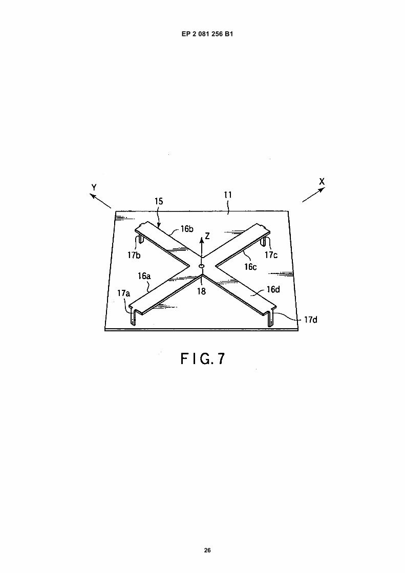
EP 2 081 256 B1
26

EP 2 081 256 B1
27

EP 2 081 256 B1
28

EP 2 081 256 B1
29

EP 2 081 256 B1
30

EP 2 081 256 B1
31

EP 2 081 256 B1
32

EP 2 081 256 B1
33

EP 2 081 256 B1
34

EP 2 081 256 B1
35

EP 2 081 256 B1
36
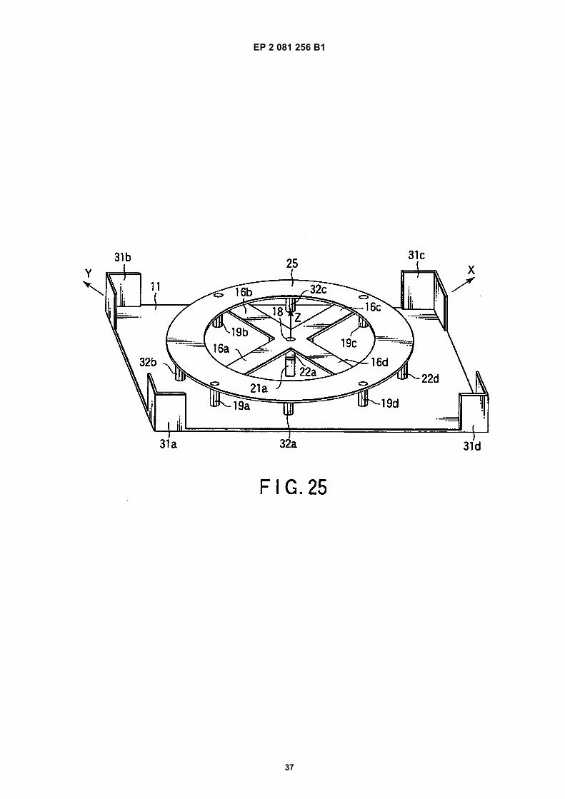
EP 2 081 256 B1
37

EP 2 081 256 B1
38

EP 2 081 256 B1
39

EP 2 081 256 B1
40

EP 2 081 256 B1
41

EP 2 081 256 B1
42

EP 2 081 256 B1
43

EP 2 081 256 B1
44

EP 2 081 256 B1
45

EP 2 081 256 B1
46

EP 2 081 256 B1
47

EP 2 081 256 B1
48

EP 2 081 256 B1
49

EP 2 081 256 B1
50

EP 2 081 256 B1
51

EP 2 081 256 B1
52

EP 2 081 256 B1
53

EP 2 081 256 B1
54

EP 2 081 256 B1
55

EP 2 081 256 B1
56

EP 2 081 256 B1
57

EP 2 081 256 B1
58

EP 2 081 256 B1
59

EP 2 081 256 B1
60

EP 2 081 256 B1
61

EP 2 081 256 B1
62

EP 2 081 256 B1
63

EP 2 081 256 B1
64

EP 2 081 256 B1
65

EP 2 081 256 B1
66

EP 2 081 256 B1
67

EP 2 081 256 B1
68

EP 2 081 256 B1
69

EP 2 081 256 B1
70

EP 2 081 256 B1
71

EP 2 081 256 B1
72

EP 2 081 256 B1
73

EP 2 081 256 B1
74

EP 2 081 256 B1
75

EP 2 081 256 B1
76
REFERENCES CITED IN THE DESCRIPTION
This list of references cited by the applicant is for the reader’s convenience only. It does not form part of the Europeanpatent document. Even though great care has been taken in compiling the references, errors or omissions cannot beexcluded and the EPO disclaims all liability in this regard.
Patent documents cited in the description
• JP 11205036 A [0003]• US 5926150 A [0004]
• US 5784032 A [0005]