1.8v 128m-bit serial nor flash with dual and quad spi&qpi
TRANSCRIPT

Zbit Semiconductor, Inc. Preliminary Datasheet 1
ZB25LQ128B
1.8V 128M-BIT
SERIAL NOR FLASH WITH DUAL AND QUAD SPI&QPI

Zbit Semiconductor, Inc. Preliminary Datasheet 2
ZB25LQ128B
Contents
FEATURES ................................................................................................................................................ 5 GENERAL DESCRIPTION ........................................................................................................................ 5
1. ORDERING INFORMATION ........................................................................................................... 7 2. BLOCK DIAGRAM .......................................................................................................................... 8 3. CONNECTION DIAGRAMS............................................................................................................ 9 4. SIGNAL DESCRIPTIONS ............................................................................................................. 10
4.1. Serial Data Input (DI) / IO0 ................................................................................................. 10 4.2. Serial Data Output (DO) / IO1 ............................................................................................ 10 4.3. Serial Clock (CLK) .............................................................................................................. 10 4.4. Chip Select (CS#) ............................................................................................................... 10 4.5. Write Protect (WP#) / IO2 .................................................................................................... 11 4.6. HOLD (HOLD#) / IO3........................................................................................................... 11 4.7. RESET (RESET#) / IO3....................................................................................................... 11
5. MEMORY ORGANIZATION .......................................................................................................... 12 5.1. Flash Memory Array ............................................................................................................ 12 5.2. Security Registers ............................................................................................................... 13
5.2.1 Security Register 0 .................................................................................................... 13 5.2.2 Serial Flash Discoverable Parameters (SFDP) Address Map .................................. 13 5.2.3 SFDP Header Field Definitions ................................................................................. 14 5.2.4 JEDEC SFDP Basic SPI Flash Parameter ............................................................... 15
6. FUNCTION DESCRIPTION .......................................................................................................... 21 6.1 SPI Operations .................................................................................................................... 21
6.1.1 SPI Modes ................................................................................................................. 21 6.1.2 Dual SPI Modes......................................................................................................... 21 6.1.3 Quad SPI Modes ....................................................................................................... 21 6.1.4 QPI Function .............................................................................................................. 22 6.1.5 Hold Function ............................................................................................................ 22 6.1.6 Software Reset & Hardware RESET# pin ................................................................. 22
6.2. Status Register ................................................................................................................... 23 6.2.1 BUSY ......................................................................................................................... 25 6.2.2 Write Enable Latch (WEL) ......................................................................................... 25 6.2.3 Block Protect Bits (BP2, BP1, BP0) .......................................................................... 25 6.2.4 Top / Bottom Block Protect (TB) ................................................................................ 25 6.2.5 Sector / Block Protect (SEC) ..................................................................................... 25 6.2.6 Complement Protect (CMP) ...................................................................................... 26 6.2.7 The Status Register Protect (SRP1, SRP0) .............................................................. 26 6.2.8 Erase / Program Suspend Status (SUS) ................................................................... 26 6.2.9 Security Register Lock Bits (LB3, LB2, LB1) ............................................................ 26 6.2.10 Quad Enable (QE) ................................................................................................... 26 6.2.11 HOLD# or RESET# Pin Function (HRSW) .............................................................. 27 6.2.12 Output Driver Strength (DRV1, DRV0) .................................................................... 27 6.2.13 High Frequency Mode Enable Bit (HFM) ................................................................ 27 6.2.14 Write Protect Selection (WPS) ................................................................................ 27
6.3. Write Protection .................................................................................................................. 27 6.3.1 Write Protect Features .............................................................................................. 27 6.3.2 Block Protection Maps ............................................................................................... 29 6.3.3 Individual Block Memory Protection (WPS=1) .......................................................... 31
6.4. Page Program ..................................................................................................................... 32 6.5. Sector Erase, Block Erase and Chip Erase ....................................................................... 32 6.6. Polling during a Write, Program or Erase Cycle ................................................................. 32 6.7. Active Power, Stand-by Power and Deep Power-Down Modes ......................................... 32
7. INSTRUCTIONS ........................................................................................................................... 33 7.1 Configuration and Status Commands .................................................................................. 38
Zbit Semiconductor, Inc. Preliminary Datasheet 3
ZB25LQ128B
7.1.1 Read Status Register (05h/35h/15h) ......................................................................... 38 7.1.2 Write Enable (06h)..................................................................................................... 38 7.1.3 Write Enable for Volatile Status Register (50h) ......................................................... 39 7.1.4 Write Disable (04h) .................................................................................................... 39 7.1.5 Write Status Register (01h/31h/11h) ......................................................................... 39
7.2 Program and Erase Commands .......................................................................................... 40 7.2.1 Page Program (PP) (02h).......................................................................................... 40 7.2.2 Quad Input Page Program (32h) ............................................................................... 41 7.2.3 Sector Erase (SE) (20h) ............................................................................................ 42 7.2.4 Block Erase (BE) (D8h) and Half Block Erase (52h) ................................................ 42 7.2.5 Chip Erase (CE) (C7h or 60h) ................................................................................... 43 7.2.6 Erase / Program Suspend (75h) ............................................................................... 44 7.2.7 Erase / Program Resume (7Ah) ................................................................................ 45
7.3 Read Commands ................................................................................................................. 45 7.3.1 Read Data (03h) ........................................................................................................ 45 7.3.2 Fast Read (0Bh) ........................................................................................................ 46 7.3.3 Fast Read Dual Output (3Bh) .................................................................................... 46 7.3.4 Fast Read Quad Output (6Bh) .................................................................................. 47 7.3.5 Fast Read Dual I/O (BBh) ......................................................................................... 47 7.3.6 Fast Read Quad I/O (EBh) ........................................................................................ 48 7.3.7 Word Read Quad I/O (E7h) ....................................................................................... 49 7.3.8 Octal Word Read Quad I/O (E3h) ............................................................................. 50 7.3.9 Set Burst with Wrap (77h) ......................................................................................... 51
7.4 Reset Commands ................................................................................................................ 52 7.4.1 Software Reset Enable (66h) .................................................................................... 52 7.4.2 Software Reset (99h) ................................................................................................ 53
7.5 ID and Security Commands ................................................................................................. 53 7.5.1 Deep Power-down (DP) (B9h) .................................................................................. 53 7.5.2 Release Power-down / Device ID (ABh) ................................................................... 53 7.5.3 Read Manufacturer / Device ID (90h) ....................................................................... 54 7.5.4 Read Identification (RDID) (9Fh/AFh) ....................................................................... 55 7.5.5 Read SFDP Register (5Ah) ....................................................................................... 55 7.5.6 Erase Security Registers (44h) ................................................................................. 56 7.5.7 Program Security Registers (42h) ............................................................................. 56 7.5.8 Read Security Registers (48h) .................................................................................. 57 7.5.9 Individual Block/Sector Lock (36h) ............................................................................ 57 7.5.10 Individual Block/Sector Unlock (39h) ...................................................................... 58 7.5.11 Read Block/Sector Lock (3Dh) ................................................................................ 59 7.5.12 Global Block/Sector Lock (7Eh) .............................................................................. 59 7.5.13 Global Block/Sector Unlock (98h) ........................................................................... 60 7.5.14 Read Manufacturer / Device ID Dual I/O (92h) ....................................................... 60 7.5.15 Read Manufacturer / Device ID Quad I/O (94h) ..................................................... 61 7.5.16 Read Unique ID Number (4Bh) ............................................................................... 61 7.5.17 Set Read Parameters (C0h) .................................................................................... 61 7.5.18 Burst Read with Wrap (0Ch) ................................................................................... 62 7.5.19 Enter QPI Mode (38h) ............................................................................................. 62 7.5.20 Exit QPI Mode (FFh) ............................................................................................... 63
8. ELECTRICAL CHARACTERISTIC ............................................................................................... 64 8.1. Absolute Maximum Ratings ................................................................................................ 65 8.2. Recommended Operating Ranges ..................................................................................... 65 8.3. DC Characteristics .............................................................................................................. 66 8.4. AC Measurement Conditions .............................................................................................. 66 8.5. AC Electrical Characteristics .............................................................................................. 67
9. PACKAGE MECHANICAL ............................................................................................................ 69 9.1. SOP8 - 208mil .................................................................................................................... 69 9.2. VSOP8 - 208mil .................................................................................................................. 69 9.3. DFN8 (5*6*0.75mm) ........................................................................................................... 70

Zbit Semiconductor, Inc. Preliminary Datasheet 4
ZB25LQ128B
9.4. DFN8 (6*8*0.75mm) ........................................................................................................... 70 9.5. TFBGA24 (5*5 Ball Array) .................................................................................................. 71 9.6. TFBGA24 (6*4 Ball Array) .................................................................................................. 71
REVISION LIST........................................................................................................................................ 72
Zbit Semiconductor, Inc. Preliminary Datasheet 5
ZB25LQ128B
FEATURES
Low power supply operation - Single 1.65V-2.0V supply
128M bit Serial Flash - 128 M-bit/16M-byte/65,536 pages - 256 bytes per programmable page - Uniform 4K-byte Sectors, 32K/64K-byte Blocks
New Family of SpiFlash Memories - Standard SPI: CLK, CS#, DI, DO, WP#, HOLD# / RESET# - Dual SPI: CLK, CS#, DI, DO, WP#, HOLD# / RESET# - Quad SPI: CLK, CS#, IO0, IO1, IO2, IO3 - QPI: CLK, CS#, IO0, IO1, IO2, IO3 - Software & Hardware Reset - Auto-increment Read capability
Temperature Ranges
- Industrial (-40°C to +85°C)
Low power consumption
- 9 uA typical standby current - 3 uA typical power down current
Efficient “Continuous Read” and QPI Mode - Continuous Read with 8/16/32/64-Byte Wrap - As few as 8 clocks to address memory - Quad Peripheral Interface(QPI) reduces instruction overhead
Flexible Architecture with 4KB sectors - Sector Erase (4K-byte) - Block Erase (32K/64K-byte) - Page Program up to 256 bytes - More than 100K erase/program cycles - More than 20-year data retention
Advanced Security Feature - Software and Hardware Write-Protect - Power Supply Lock-Down and OTP protection - Top/Bottom, Complement array protection - 128-Bit Unique ID for each device - Discoverable parameters(SFDP) register - 3X1024-Byte Security Registers with OTP locks - Volatile & Non-volatile Status Register Bits
High performance program/erase speed - Page program time: 500us typical - Sector erase time: 50ms typical - Block erase time: 300ms typical - Chip erase time: 60s typical
Package Options - SOP8 - 208mil - VSOP8 - 208mil - DFN8 (5*6*0.75mm)/(6*8*0.75mm) - TFBGA24 - All Pb-free packages are RoHS compliant
GENERAL DESCRIPTION
The ZB25LQ128B of non-volatile flash memory device supports the standard Serial Peripheral Interface (SPI). Traditional SPI single bit serial input and output (Single I/O or SIO) is supported as well as optional two bit (Dual I/O or DIO) and four bit (quad I/O or QIO) serial protocols. This multiple width interface is called SPI Multi-I/O or MIO.
The SPI protocols use only 4 to 6 signals: Chip Select (CS#) Serial Clock (CLK) Serial Data
- IO0 (DI) - IO1 (DO) - IO2 (WP#) - IO3 (HOLD# / RESET#)

Zbit Semiconductor, Inc. Preliminary Datasheet 6
ZB25LQ128B
The ZB25LQ128B support the standard Serial Peripheral Interface (SPI), Dual/Quad I/O SPI as well as 2-clocks instruction cycle Quad Peripheral Interface (QPI): Serial Clock, Chip Select, Serial Data I/O0 (DI), I/O1 (DO), I/O2 (WP#), and I/O3 (HOLD# / RESET#). SPI clock frequencies of up to 104MHz are supported allowing equivalent clock rates of 208MHz (104MHz x 2) for Dual I/O and 416MHz (104MHz x 4) for Quad I/O when using the Fast Read Dual/Quad I/O and QPI instructions. These transfer rates can outperform standard Asynchronous 8 and 16-bit Parallel Flash memories. The Continuous Read Mode allows for efficient memory access with as few as 8-clocks of instruction-overhead to read a 24-bit address, allowing true XIP (execute in place) operation.
A Hold pin, Write Protect pin and programmable write protection, with top or bottom array control, provide
further control flexibility. Additionally, the device supports JEDEC standard manufacturer and device ID and SFDP Register, a 128-bit Unique Serial Number and three 1024-byte Security Registers.
The ZB25LQ128B provides an ideal storage solution for systems with limited space, signal connections,
and power. These memories' flexibility and performance is better than ordinary serial flash devices. They are ideal for code shadowing to RAM, executing code directly (XIP), and storing reprogrammable data.
Zbit Semiconductor, Inc. Preliminary Datasheet 7
ZB25LQ128B
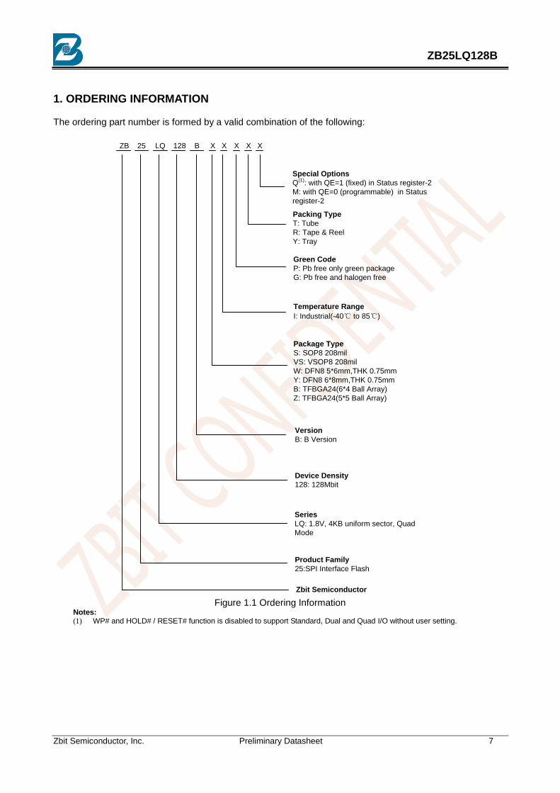
1. ORDERING INFORMATION
The ordering part number is formed by a valid combination of the following:
128 B XX X X
Packing Type
T: Tube
R: Tape & Reel
Y: Tray
Green Code
P: Pb free only green package
G: Pb free and halogen free
Temperature Range
I: Industrial(-40℃ to 85℃)
Package Type
S: SOP8 208mil
VS: VSOP8 208mil
W: DFN8 5*6mm,THK 0.75mm
Y: DFN8 6*8mm,THK 0.75mm
B: TFBGA24(6*4 Ball Array)
Z: TFBGA24(5*5 Ball Array)
Version
B: B Version
Product Family
25:SPI Interface Flash
Zbit Semiconductor
LQZB 25
Series
LQ: 1.8V, 4KB uniform sector, Quad
Mode
Device Density
128: 128Mbit
X
Special Options
Q(1)
: with QE=1 (fixed) in Status register-2
M: with QE=0 (programmable) in Status
register-2
Figure 1.1 Ordering Information
Notes: (1) WP# and HOLD# / RESET# function is disabled to support Standard, Dual and Quad I/O without user setting.
Zbit Semiconductor, Inc. Preliminary Datasheet 8
ZB25LQ128B
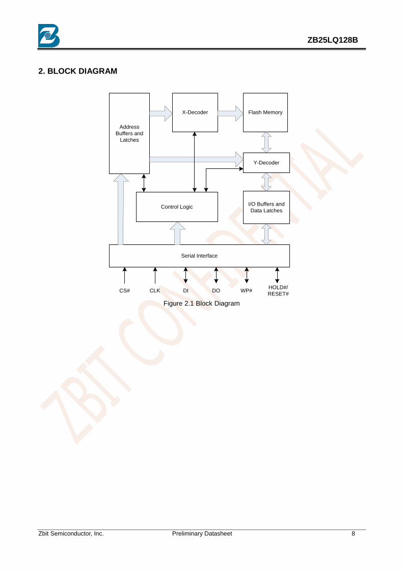
2. BLOCK DIAGRAM
Address
Buffers and
Latches
X-Decoder Flash Memory
Y-Decoder
I/O Buffers and
Data LatchesControl Logic
Serial Interface
CS# CLK DI DO WP#HOLD#/
RESET#
Figure 2.1 Block Diagram

Zbit Semiconductor, Inc. Preliminary Datasheet 9
ZB25LQ128B
3. CONNECTION DIAGRAMS
CS#
DO
WP#
GND
VCC
HOLD# /
RESET#
CLK
DI
1
2
3
4 5
6
7
8
Figure 3.1 SOP8 (150/208mil)/ DIP8 (300mil)
CS#
DO
WP#
GND
VCC
HOLD# /
RESET#
CLK
DI
1
2
3
4 5
6
7
8
Figure 3.2 DFN8( 5*6 mm)

Zbit Semiconductor, Inc. Preliminary Datasheet 10
ZB25LQ128B
4. SIGNAL DESCRIPTIONS
Table 4.1 Pin Descriptions
Symbol Pin Name
CLK Serial Clock Input
DI(IO0) Serial Data Input(Data input output 0) (1)
DO(IO1) Serial Data Output(Data input output 1) (1)
CS# Chip Enable
WP#(IO2)(3)
Write Protect (Data input output 2) (2)
HOLD# / RESET#(3)
(IO3) Hold or Reset input(Data input output 3) (2)
VCC Power Supply (1.65-2.0V)
GND Ground
Notes: (1) IO0 and IO1 are used for Standard and Dual SPI instructions. (2) IO0—IO3 are used for QUAD SPI / QPI instructions. (3) WP# and HOLD# / RESET# functions are only available for Standard and Dual SPI.
4.1. Serial Data Input (DI) / IO0
The SPI Serial Data Input (DI) pin is used to transfer data serially into the device. It receives instructions,
address and data to be programmed. Data is latched on the rising edge of the Serial Clock (CLK) input pin. The DI pin becomes IO0 - an input and output during Dual and Quad commands for receiving instructions, address, and data to be programmed (values latched on rising edge of serial CLK clock signal) as well as shifting out data (on the falling edge of CLK).
4.2. Serial Data Output (DO) / IO1
The SPI Serial Data Output (DO) pin is used to transfer data serially out of the device. Data is shifted out
on the falling edge of the Serial Clock (CLK) input pin. DO becomes IO1 - an input and output during Dual and Quad commands for receiving instructions, addresses, and data to be programmed (values latched on rising edge of serial CLK clock signal) as well as shifting out data (on the falling edge of CLK).
4.3. Serial Clock (CLK)
The SPI Serial Clock Input (CLK) pin provides the timing for serial input and output operations. ("See SPI
Mode")
4.4. Chip Select (CS#)
The SPI Chip Select (CS#) pin enables and disables device operation. When CS# is high the device is
deselected and the Serial Data Output pins are at high impedance.
When deselected, the devices power consumption will be at standby levels unless an internal erase, program or status register cycle is in progress. When CS# is brought low the device will be selected, power consumption will increase to active levels and instructions can be written to and data read from the device. After power-up, CS# must transition from high to low before a new instruction will be accepted.

Zbit Semiconductor, Inc. Preliminary Datasheet 11
ZB25LQ128B
4.5. Write Protect (WP#) / IO2
The Write Protect (WP#) pin can be used to prevent the Status Register from being written. Used in
conjunction with the Status Register‘s Block Protect (BP0, BP1 and BP2, TB, SEC, CMP) bits and Status Register Protect (SRP0) bits, a portion or the entire memory array can be hardware protected.
The WP# function is not available when the Quad mode is enabled. The WP# function is replaced by IO2
for input and output during Quad mode for receiving addresses and data to be programmed (values are latched on rising edge of the CLK signal) as well as shifting out data (on the falling edge of CLK).
4.6. HOLD (HOLD#) / IO3
The HOLD# pin allows the device to be paused while it is actively selected. When HRSW bit is ‗0‘ (factory
default is ‗0‘), the HOLD# pin is enabled. When HOLD# is brought low, while CS# is low, the DO pin will be at high impedance and signals on the DI and CLK pins will be ignored (don‘t care). When HOLD# is brought high, device operation can resume. The HOLD# function can be useful when multiple devices are sharing the same SPI signals. The HOLD# pin is active low. When the QE bit of Status Register-2 is set for Quad I/O, the HOLD# pin function is not available since this pin is used for IO3.
4.7. RESET (RESET#) / IO3
The RESET# pin allows the device to be reset by the controller. When HRSW bit is ‗1‘ (factory default is
‗0‘), the RESET# pin is enabled. Drive RESET# low for a minimum period of ~1us (tRESET*) will interrupt any on-going external/internal operations, regardless the status of other SPI signals (CS#, CLK, DI, DO, WP# and/or HOLD#). The Hardware Reset function is only available for standard SPI and Dual SPI operation, when QE=0, the IO3 pin can be configured either as a HOLD# pin or as a RESET# pin depending on Status Register setting, when QE=1, this pin is the Serial Data IO (IO3) for Quad I/O operation.

Zbit Semiconductor, Inc. Preliminary Datasheet 12
ZB25LQ128B
5. MEMORY ORGANIZATION
5.1. Flash Memory Array
The memory is organized as: - 16,777,216bytes - Uniform Sector Architecture 256 blocks of 64-Kbyte - 4,096 sectors of 4-Kbyte - 65,536 pages (256 bytes each)
Each page can be individually programmed (bits are programmed from 1 to 0). The device is Sector,
Block or Chip Erasable but not Page Erasable.
Table 5.1(1)
Memory Organization(ZB25LQ128B) Block/ Security Register/SFDP
Sector Address range
Security Register 3 - 003000H 0033FFH
Security Register 2 - 002000H 0023FFH
Security Register 1 - 001000H 0013FFH
Security Register 0 (SFDP)
- 000000H 0000FFH
Block 255
4095 FFF000H FFFFFFH
...... ...... ......
4080 FF0000H FF0FFFH
Block 254
4079 FEF000H FEFFFFH
...... ...... ......
4064 FE0000H FE0FFFH
......
...... ...... ......
...... ...... ......
...... ...... ......
......
...... ...... ......
...... ...... ......
...... ...... ......
Block 2
47 02F000H 02FFFFH
...... ...... ......
32 020000H 020FFFH
Block 1
31 01F000H 01FFFFH
...... ...... ......
16 010000H 010FFFH
Block 0
15 00F000H 00FFFFH
...... ...... ......
0 000000H 000FFFH
Notes: (1) These are condensed tables that use a couple of sectors as references. There are address ranges that are not explicitly listed. All 4-kB sectors have the pattern XXX000h-XXXFFFh.

Zbit Semiconductor, Inc. Preliminary Datasheet 13
ZB25LQ128B
5.2. Security Registers
The ZB25LQ128B provides three 1024-byte Security Registers. Each register can be used to store information that can be permanently protected by programming One Time Programmable (OTP) lock bits in Status Register-2.
Register 0 is used by ZBIT to store and protect the Serial Flash Discoverable Parameters (SFDP)
information that is also accessed by the Read SFDP command. See Table 5.1. The three additional Security Registers can be erased, programmed, and protected individually. These
registers may be used by system manufacturers to store and permanently protect security or other important information separate from the main memory array.
5.2.1 Security Register 0 Serial Flash Discoverable Parameters (SFDP — JEDEC JESD216D):
This document defines the Serial Flash Discoverable Parameters (SFDP) revision D data structure for
ZB25LQ128B family.
The Read SFDP (RSFDP) command (5Ah) reads information from a separate flash memory address space for device identification, feature, and configuration information, in accord with the JEDEC JESD216D standard for Serial Flash Discoverable Parameters.
The SFDP data structure consists of a header table that identifies the revision of the JESD216 header format that is supported and provides a revision number and pointer for each of the SFDP parameter tables that are provided. The parameter tables follow the SFDP header. However, the parameter tables may be placed in any physical location and order within the SFDP address space. The tables are not necessarily adjacent nor in the same order as their header table entries. The SFDP header points to the following parameter tables: Basic Flash – This is the original SFDP table.
The physical order of the tables in the SFDP address space is: SFDP Header, and Basic Flash. The SFDP address space is programmed by ZBIT and read-only for the host system. 5.2.2 Serial Flash Discoverable Parameters (SFDP) Address Map
The SFDP address space has a header starting at address zero that identifies the SFDP data structure and provides a pointer to each parameter. One Basic Flash parameter is mandated by the JEDEC JESD216D standard.
Table 5.2 SFDP Overview Map — Security Register 0 Byte Address Description
0000h Location zero within JEDEC JESD216D SFDP space – start of SFDP header
0020h Undefined space reserved for future SFDP header
0030h Start of SFDP parameter
... Remainder of SFDP JEDEC parameter followed by undefined space
007Bh End of SFDP space
007Ch to 00FFh Reserved space
Zbit Semiconductor, Inc. Preliminary Datasheet 14
ZB25LQ128B
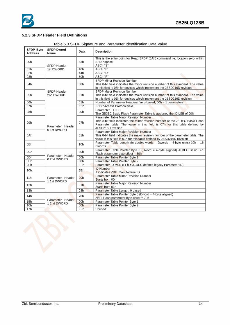
5.2.3 SFDP Header Field Definitions
Table 5.3 SFDP Signature and Parameter Identification Data Value
SFDP Byte Address
SFDP Dword Name
Data Description
00h
SFDP Header 1st DWORD
53h This is the entry point for Read SFDP (5Ah) command i.e. location zero within SFDP space ASCII ―S‖
01h 46h ASCII ―F‖
02h 44h ASCII ―D‖
03h 50h ASCII ―P‖
04h
SFDP Header 2nd DWORD
08h SFDP Minor Revision Number This 8-bit field indicates the minor revision number of this standard. The value in this field is 08h for devices which implement the JESD216D revision
05h 01h SFDP Major Revision Number This 8-bit field indicates the major revision number of this standard. The value in this field is 01h for devices which implement the JESD216D revision
06h 01h Number of Parameter Headers (zero based, 00h = 1 parameters)
07h FFh SFDP Access Protocol field
08h
Parameter Header 0 1st DWORD
00h Parameter ID LSB The JEDEC Basic Flash Parameter Table is assigned the ID LSB of 00h.
09h 07h
Parameter Table Minor Revision Number This 8-bit field indicates the minor revision number of the JEDEC Basic Flash Parameter table. The value in this field is 07h for this table defined by JESD216D revision
0Ah 01h Parameter Table Major Revision Number This 8-bit field indicates the major revision number of the parameter table. The value in this field is 01h for this table defined by JESD216D revision
0Bh 10h Parameter Table Length (in double words = Dwords = 4-byte units) 10h = 16 Dwords
0Ch
Parameter Header 0 2nd DWORD
30h Parameter Table Pointer Byte 0 (Dword = 4-byte aligned) JEDEC Basic SPI Flash parameter byte offset = 30h
0Dh 00h Parameter Table Pointer Byte 1
0Eh 00h Parameter Table Pointer Byte 2
0Fh FFh Parameter ID MSB (FFh = JEDEC defined legacy Parameter ID)
10h
Parameter Header 1 1st DWORD
5Eh ID Number It indicates ZBIT manufacture ID
11h 00h Parameter Table Minor Revision Number Starts from 00h
12h 01h Parameter Table Major Revision Number Starts from 01h
13h 03h Parameter Table Length, 0 based
14h
Parameter Header 1 2nd DWORD
70h Parameter Table Pointer Byte 0 (Dword = 4-byte aligned) ZBIT Flash parameter byte offset = 70h
15h 00h Parameter Table Pointer Byte 1
16h 00h Parameter Table Pointer Byte 2
17h FFh Unused

Zbit Semiconductor, Inc. Preliminary Datasheet 15
ZB25LQ128B
5.2.4 JEDEC SFDP Basic SPI Flash Parameter
Table 5.4 Basic SPI Flash Parameter, JEDEC SFDP Rev D (Sheet 1 of 5) SFDP Parameter Relative Byte Address
SFDP Dword Name
Data Description
30h
JEDEC Basic Flash Parameter Dword-1
E5h
Start of SFDP JEDEC parameter Bits 7:5 = unused = 111b Bit 4:3 = 05h is volatile status register write instruction and status register is default non-volatile= 00b Bit 2 = Program Buffer > 64 bytes = 1 Bits 1:0 = Uniform 4-kB erase is supported throughout the device = 01b
31h 20h Bits 15:8 = Uniform 4-kB erase instruction = 20h
32h F1h
Bit 23 = Unused = 1b Bit 22 = Supports QOR Read (1-1-4), Yes = 1b Bit 21 = Supports QIO Read (1-4-4),Yes =1b Bit 20 = Supports DIO Read (1-2-2), Yes = 1b Bit19 = Supports DDR, No= 0 b Bit 18:17 = Number of Address Bytes 3 only = 00b Bit 16 = Supports SIO and DIO Yes = 1b Binary Field: 1-1-1-1-0-00-1 Nibble Format: 1111_0001 Hex Format: F1
33h FFh Bits 31:24 = Unused = FFh
34h JEDEC Basic Flash Parameter Dword-2
FFh Density in bits, zero based, 32 Mb = 01FFFFFFh 64 Mb = 03FFFFFFh 128 Mb = 07FFFFFFh
35h FFh
36h FFh
37h 07h
38h
JEDEC Basic Flash Parameter Dword-3
44h Bits 7:5 = number of QIO (1-4-4)Mode cycles = 010b Bits 4:0 = number of Fast Read QIO Dummy cycles = 00100b for default latency code
39h EBh Fast Read QIO (1-4-4)instruction code
3Ah 08h Bits 23:21 = number of Quad Out (1-1-4) Mode cycles = 000b Bits 20:16 = number of Quad Out Dummy cycles = 01000b for default latency code
3Bh 6Bh Quad Out (1-1-4)instruction code
3Ch
JEDEC Basic Flash Parameter Dword-4
08h Bits 7:5 = number of Dual Out (1-1-2)Mode cycles = 000b Bits 4:0 = number of Dual Out Dummy cycles = 01000b for default latency code
3Dh 3Bh Dual Out (1-1-2) instruction code
3Eh 80h Bits 23:21 = number of Dual I/O Mode cycles = 100b Bits 20:16 = number of Dual I/O Dummy cycles = 00000b for default latency code
3Fh BBh Dual I/O instruction code
40h JEDEC Basic Flash Parameter Dword-5
FEh
Bits 7:5 RFU = 111b Bit 4 = QPI (4-4-4) fast read commands supported = 1b Bits 3:1 RFU = 111b Bit 0 = Dual All not supported = 0b
41h FFh Bits 15:8 = RFU = FFh
42h FFh Bits 23:16 = RFU = FFh
43h FFh Bits 31:24 = RFU = FFh
44h JEDEC Basic Flash Parameter Dword-6
FFh Bits 7:0 = RFU = FFh
45h FFh Bits 15:8 = RFU = FFh
46h FFh Bits 23:21 = number of Dual All Mode cycles = 111b Bits 20:16 = number of Dual All Dummy cycles = 11111b
47h FFh Dual All instruction code

Zbit Semiconductor, Inc. Preliminary Datasheet 16
ZB25LQ128B
Table 5.4 Basic SPI Flash Parameter, JEDEC SFDP Rev D (Sheet 2 of 5)
SFDP Parameter Relative Byte Address
SFDP Dword Name
Data Description
48h JEDEC Basic Flash Parameter Dword-7
FFh Bits 7:0 = RFU = FFh
49h FFh Bits 15:8 = RFU = FFh
4Ah 44h Bits 23:21 = number of QPI Mode cycles = 010b Bits 20:16 = number of QPI Dummy cycles = 00100b for default latency code
4Bh EBh QPI instruction code
4Ch JEDEC Basic Flash Parameter Dword-8
0Ch Erase Type 1 size 2N Bytes = 4 kB = 0Ch (for Uniform 4 kB)
4Dh 20h Erase Type 1 instruction
4Eh 0Fh Erase Type 2 size 2N Bytes = 32 kB = 0Fh (for Uniform 32 kB)
4Fh 52h Erase Type 2 instruction
50h JEDEC Basic Flash Parameter Dword-9
10h Erase Type 3 size 2N Bytes =64 kB = 10h(for Uniform 64 kB)
51h D8h Erase Type 3 instruction
52h 00h Erase Type 4 size 2N Bytes = not supported = 00h
53h FFh Erase Type 4 instruction = not supported = FFh
54h
JEDEC Basic Flash Parameter Dword-10
31h Bits 31:30 = Erase Type 4 Erase, Typical time units (00b: 1 ms, 01b: 16 ms, 10b: 128 ms, 11b:1 s) = RFU = 11b Bits 29:25 = Erase Type 4 Erase, Typical time count = RFU = 11111b (typ erase time = (count+1) * units) = RFU =11111 Bits 24:23 = Erase Type 3 Erase, Typical time units (00b: 1 ms, 01b: 16 ms, 10b: 128 ms, 11b:1 s) = RFU = 01b Bits 22:18 = Erase Type 3 Erase, Typical time count = 10010b (typ erase time = (count +1) *units) = 19*16 ms =300ms Bits 17:16 = Erase Type 2 Erase, Typical time units (00b: 1 ms, 01b: 16 ms, 10b: 128 ms, 11b:1 s) = 16 ms = 01b Bits 15:11 = Erase Type 2 Erase, Typical time count = 01100b (typ erase time = (count +1) *units) = 12*16 ms = 180 ms Bits 10:9 = Erase Type 1 Erase, Typical time units (00b: 1 ms, 01b: 16 ms, 10b: 128 ms, 11b: 1s) = 16ms = 01b Bits 8:4 = Erase Type 1 Erase, Typical time count = 00011b (typ erase time = (count +1) *units) = 4*16 ms = 50 ms Bits 3:0 = Count = (Max Erase time / (2 * Typical Erase time))- 1 = 0001b Multiplier from typical erase time to maximum erase time = 8x multiplier Max Erase time = 2*(Count +1)*Typ Erase time Binary Fields: 1111111_0110010_0101100_0100011_0001 Nibble Format: 1111_1110_1100_1001_0110_0010_0011_0001 Hex Format: FE_C9_62_31
55h 62h
56h C9h
57h FEh
Zbit Semiconductor, Inc. Preliminary Datasheet 17
ZB25LQ128B
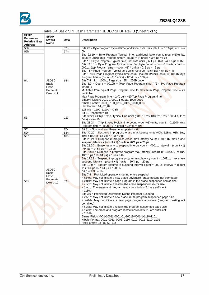
Table 5.4 Basic SPI Flash Parameter, JEDEC SFDP Rev D (Sheet 3 of 5) SFDP Parameter Relative Byte Address
SFDP Dword Name
Data Description
58h
JEDEC Basic Flash Parameter Dword-11
82h Bits 23 = Byte Program Typical time, additional byte units (0b:1 μs, 1b:8 μs) = 1 μs = 0b Bits 22:19 = Byte Program Typical time, additional byte count, (count+1)*units, count = 0010b,(typ Program time = (count +1) * units) = 3*1 μs =3 μs Bits 18 = Byte Program Typical time, first byte units (0b:1 μs, 1b:8 μs) = 8 μs = 1b Bits 17:14 = Byte Program Typical time, first byte count, (count+1)*units, count = 0001b, (typ Program time = (count +1) * units) = 2*8 μs = 16 μs Bits 13 = Page Program Typical time units (0b:8 μs, 1b:64 μs) = 64 μs = 1b Bits 12:8 = Page Program Typical time count, (count+1)*units, count = 00111b, (typ Program time = (count +1) * units) = 8*64 μs = 500 μs Bits 7:4 = N = 1000b, Page size= 2N = 256B page Bits 3:0 = Count = 0010b = (Max Page Program time / (2 * Typ Page Program time))- 1 Multiplier from typical Page Program time to maximum Page Program time = 2x multiplier Max Page Program time = 2*(Count +1)*Typ Page Program time Binary Fields: 0-0010-1-0001-1-00111-1000-0010 Nibble Format: 0001_0100_0110_0111_1000_0010 Hex Format: 14_67_82
59h 67h
5Ah 14h
5Bh CEh
128 Mb = 1100_1110b = CEh Bit 31 Reserved = 1b Bits 30:29 = Chip Erase, Typical time units (00b: 16 ms, 01b: 256 ms, 10b: 4 s, 11b: 64 s) = 4s= 10b Bits 28:24 = Chip Erase, Typical time count, (count+1)*units, count = 01110b, (typ Program time = (count +1) * units) = 15*4s = 60s
5Ch
JEDEC Basic Flash Parameter Dword-12
EDh Bit 31 = Suspend and Resume supported = 0b Bits 30:29 = Suspend in-progress erase max latency units (00b: 128ns, 01b: 1us, 10b: 8 μs,11b: 64 μs) = 1 μs= 01b Bits 28:24 = Suspend in-progress erase max latency count = 10011b, max erase suspend latency = (count +1) * units = 20*1 μs = 20 μs Bits 23:20 = Erase resume to suspend interval count = 0001b, interval = (count +1) * 64 μs = 2* 64 μs = 128 μs Bits 19:18 = Suspend in-progress program max latency units (00b: 128ns, 01b: 1us, 10b: 8 μs,11b: 64 μs) = 1 μs= 01b Bits 17:13 = Suspend in-progress program max latency count = 10011b, max erase suspend latency = (count +1) * units = 20*1 μs = 20 μs Bits 12:9 = Program resume to suspend interval count = 0001b, interval = (count +1) * 64 μs =2 * 64 μs = 128 μs Bit 8 = RFU = 1b Bits 7:4 = Prohibited operations during erase suspend = xxx0b: May not initiate a new erase anywhere (erase nesting not permitted) + xx1xb: May not initiate a page program in the erase suspended sector size + x1xxb: May not initiate a read in the erase suspended sector size + 1xxxb: The erase and program restrictions in bits 5:4 are sufficient = 1110b Bits 3:0 = Prohibited Operations During Program Suspend = xxx1b: May not initiate a new erase in the program suspended page size + xx0xb: May not initiate a new page program anywhere (program nesting not permitted) + x1xxb: May not initiate a read in the program suspended page size + 1xxxb: The erase and program restrictions in bits 1:0 are sufficient = 1101b Binary Fields: 0-01-10011-0001-01-10011-0001-1-1110-1101 Nibble Format: 0011_0011_0001_0110_0110_0011_1110_1101 Hex Format: 33_16_63_ED
5Dh 63h
5Eh 16h
5Fh 33h

Zbit Semiconductor, Inc. Preliminary Datasheet 18
ZB25LQ128B
Table 5.4 Basic SPI Flash Parameter, JEDEC SFDP Rev D (Sheet 4 of 5)
SFDP Parameter Relative Byte Address
SFDP Dword Name
Data Description
60h JEDEC Basic Flash Parameter Dword-13
7Ah Bits 31:24 = Erase Suspend Instruction = 75h Bits 23:16 = Erase Resume Instruction = 7Ah Bits 15:8 = Program Suspend Instruction = 75h Bits 7:0 = Program Resume Instruction = 7Ah
61h 75h
62h 7Ah
63h 75h
64h
JEDEC Basic Flash Parameter Dword-14
F7h Bit 31 = Deep Power-Down Supported = 0 Bits 30:23 = Enter Deep Power-Down Instruction = B9h Bits 22:15 = Exit Deep Power-Down Instruction = ABh Bits 14:13 = Exit Deep Power-Down to next operation delay units = (00b: 128 ns, 01b: 1 μs, 10b: 8 μs, 11b: 64 μs) = 1 μs = 01b Bits 12:8 = Exit Deep Power-Down to next operation delay count = 00010b, Exit Deep Power-Down to next operation delay = (count+1)*units = 3*1 μs=3 μs Bits 7:4 = RFU = 1111b Bit 3:2 = Status Register Polling Device Busy = 01b: Legacy status polling supported = Use legacy polling by reading the Status Register with 05h instruction and checking WIP bit[0] (0=ready; 1=busy). Bits 1:0 = RFU = 11b Binary Fields: 0-10111001-10101011-01-00010-1111-01-11 Nibble Format: 0101_1100_1101_0101_1010_0010_1111_0111 Hex Format: 5C_D5_A2_F7
65h A2h
66h D5h
67h 5Ch
68h
JEDEC Basic Flash Parameter Dword-15
19h Bits 31:24 = RFU = FFh Bit 23 = Hold and WP Disable = set QE(bit 1 of SR2) high = 1b Bits 22:20 = Quad Enable Requirements = 101b: QE is bit 1 of the status register 2. Status register 1 is read using Read Status instruction 05h. Status register 2 is read using instruction 35h. QE is set via Write Status instruction 01h with two data bytes where bit 1 of the second byte is one. It is cleared via Write Status with two data bytes where bit 1 of the second byte is zero. Bits 19:16 0-4-4 Mode Entry Method = xxx1b: Mode Bits[7:0] = A5h Note: QE must be set prior to using this mode + x1xxb: Mode Bits[7:0] = Axh + 1xxxb: RFU = 1101b Bits 15:10 0-4-4 Mode Exit Method = xx_xxx1b: Mode Bits[7:0] = 00h will terminate this mode at the end of the current read operation + xx_1xxxb: Input Fh (mode bit reset) on DQ0-DQ3 for 8 clocks. This will terminate the mode prior to the next read operation. + 11_x1xx: RFU = 111101b Bit 9 = 0-4-4 mode supported = 1 Bits 8:4 = 4-4-4 mode enable sequences = 0_0001b: set QE per QER description above, then issue instruction 38h Bits 3:0 = 4-4-4 mode disable sequences = xxx1b: issue FFh instruction + 1xxxb: issue the Soft Reset 66/99 sequence = 1001b Binary Fields: 11111111-1-101-1101-111101-1-00001-1001 Nibble Format: 1111_1111-1101-1101-1111_0110_0001-1001 Hex Format: FF_DD_F6_19
69h F6h
6Ah DDh
6Bh FFh

Zbit Semiconductor, Inc. Preliminary Datasheet 19
ZB25LQ128B
Table 5.4 Basic SPI Flash Parameter, JEDEC SFDP Rev D (Sheet 5 of 5)
SFDP Parameter Relative Byte Address
SFDP Dword Name
Data Description
6Ch
JEDEC Basic Flash Parameter Dword-16
E8h Bits 31:24 = Enter 4-Byte Addressing = xxxx_xxx1b:issue instruction B7 (preceding write enable not required + xx1x_xxxxb: Supports dedicated 4-byte address instruction set. Consult vendor data sheet for the instruction set definition or look for 4-byte Address Parameter Table. + 1xxx_xxxxb: Reserved = 10000000b not supported Bits 23:14 = Exit 4-byte Addressing = xx_xxxx_xxx1b:issue instruction E9h to exit 4-byte address mode (Write enable instruction 06h is not required) + xx_xx1x_xxxxb: Hardware reset + xx_x1xx_xxxxb: Software reset (see bits 13:8 in this DWORD) + xx_1xxx_xxxxb: Power cycle + x1_xxxx_xxxxb: Reserved + 1x_xxxx_xxxxb: Reserved = 11_0000_0000b not supported Bits 13:8 = Soft Reset and Rescue Sequence Support = x1_xxxxb: issue reset enable instruction 66h, then issue reset instruction 99h. The reset enable, reset sequence may be issued on 1,2, or 4 wires depending on the device operating mode + 1x_xxxxb: exit 0-4-4 mode is required prior to other reset sequences above if the device may be operating in this mode. = 11_0000b Bit 7 = RFU = 1 Bits 6:0 = Volatile or Non-Volatile Register and Write Enable Instruction for Status Register 1 = xxx_1xxxb: Non-Volatile/Volatile status register 1 powers-up to last written value in the nonvolatile status register, use instruction 06h to enable write to non-volatile status register. Volatile status register may be activated after power-up to override the non-volatile status register, use instruction 50h to enable write and activate the volatile status register. + x1x_xxxxb: Reserved + 1xx_xxxxb: Reserved = 1101000b Binary Fields: 10000000-1100000000-110000-1-1101000 Nibble Format: 1000_0000_1100_0000_0011_0000_1110_1000 Hex Format: 80_C0_30_E8
6Dh 30h
6Eh C0h
6Fh 80h

Zbit Semiconductor, Inc. Preliminary Datasheet 20
ZB25LQ128B
Table 5.5 ZBIT flash parameter SFDP Parameter Relative Byte Address
SFDP Dword Name
Data Description
70h
ZBIT flash parameter Dword-1
00h Bits 15:0 = Vcc Supply Maximum Voltage 2000h = 2.000 V 2700h = 2.700 V 3600h = 3.600 V
71h 20h
72h 50h Bits 31:16 = Vcc Supply Minimum Voltage 1650h = 1.650V 2250h = 2.250V 2350h = 2.350V 2700h = 2.700V
73h 16h
74h
ZBIT flash parameter Dword-2
9Fh Bit 0 = HW Reset# pin ( 0=not support, 1=support ) = 1b Bit 1 = HW Hold# pin ( 0=not support, 1=support ) = 1b Bit 2 = Deep Power Down Mode ( 0=not support, 1=support ) = 1b Bit 3 = SW Reset ( 0=not support, 1=support ) = 1b Bits 11:4 = SW Reset Opcode: Should be issue Reset Enable(66H) before Reset cmd = 10011001b Bit 12 = Program Suspend/Resume ( 0=not support, 1=support ) = 1b Bit 13 = Erase Suspend/Resume ( 0=not support, 1=support ) = 1b Bit 14 = Unused = 1b Bit 15 = Wrap-Around Read mode ( 0=not support, 1=support ) = 1b Binary Fields: 1111_10011001_1111 Nibble Format: 1111_1001_1001_1111 Hex Format: F9_9F
75h F9h
76h 77h Wrap-Around Read mode Opcode
77h 64h
Wrap-Around Read data length 08H:support 8B wrap-around read 16H:8B&16B 32H:8B&16B&32B 64H:8B&16B&32B&64B
78h
ZBIT flash parameter Dword-3
B1h Bit 0 = Individual block lock ( 0=not support, 1=support ) = 1b Bit 1 = Individual block lock bit (Volatile/Nonvolatile) ( 0=Volatile, 1=Nonvolatile ) = 0b Bits 9:2 = Individual block lock Opcode = 00110110b Bit 10 = Individual block lock Volatile protect bit default protect status ( 0=protect, 1=unprotect ) = 0b Bit 11 = Secured OTP ( 0=not support, 1=support ) = 1b Bit 12 = Read Lock ( 0=not support, 1=support ) = 0b Bit 13 = Permanent Lock ( 0=not support, 1=support ) = 0b/1b
(1)
Bits 15:14 = Unused = 11b Binary Fields: 110(1)010_01101100_01 Nibble Format: 110(1)0_1001_1011_0001 Hex Format: C(E)9_B1
79h C(E)9h
7Ah FFh Unused
7Bh FFh Unused
NOTE: (1) ZB25LQ128B support Permanent Lock. Please contact ZBIT for details.

Zbit Semiconductor, Inc. Preliminary Datasheet 21
ZB25LQ128B
6. FUNCTION DESCRIPTION
6.1 SPI Operations
6.1.1 SPI Modes
The ZB25LQ128B can be driven by an embedded microcontroller (bus master) in either of the two
following clocking modes.
Mode 0 with Clock Polarity (CPOL) = 0 and, Clock Phase (CPHA) = 0 Mode 3 with CPOL = 1 and, CPHA = 1
For these two modes, input data is always latched in on the rising edge of the CLK signal and the output data is always available on the falling edge of the CLK clock signal.
The difference between the two modes is the clock polarity when the bus master is in standby mode and
not transferring any data.
CLK will stay at logic low state with CPOL = 0, CPHA = 0 CLK will stay at logic high state with CPOL = 1, CPHA = 1
CS#
CPOL=0_CPHA=0_CLK
DI
DO
MSB
MSB
CPOL=1_CPHA=1_CLK
Figure 6.1 SPI Modes
Timing diagrams throughout the rest of the document are generally shown as both mode 0 and 3 by
showing CLK as both high and low at the fall of CS#. In some cases a timing diagram may show only mode 0 with CLK low at the fall of CS#. In such case, mode 3 timing simply means clock is high at the fall of CS# so no CLK rising edge set up or hold time to the falling edge of CS# is needed for mode 3.
CLK cycles are measured (counted) from one falling edge of CLK to the next falling edge of CLK. In mode 0 the beginning of the first CLK cycle in a command is measured from the falling edge of CS# to the first falling edge of CLK because CLK is already low at the beginning of a command. 6.1.2 Dual SPI Modes
The ZB25LQ128B supports Dual SPI Operation when using the Fast Read Dual Output (3Bh) and Fast
Dual I/O (BBh) instruction. These features allow data to be transferred from the device at twice the rate possible with the standard SPI. These instructions are ideal for quickly downloading code to RAM upon Power-up (code-shadowing) or for executing non-speed-critical code directly from the SPI bus (XIP). When using Dual SPI commands, the DI and DO pins become bidirectional I/O pins: IO0 and IO1.
6.1.3 Quad SPI Modes
The ZB25LQ128B supports Quad SPI operation when using the Fast Read Quad Output (6Bh), Fast
Read Quad I/O (EBh) instruction, Word Read Quad I/O(E7h), and Octal Word Read Quad I/O(E3h). These instructions allow data to be transferred to or from the device four times the rate of ordinary Serial Flash. The Quad Read instructions offer a significant improvement in continuous and random access transfer rates allowing fast code-shadowing to RAM or execution directly from the SPI bus (XIP). When using Quad SPI

Zbit Semiconductor, Inc. Preliminary Datasheet 22
ZB25LQ128B
instructions, the DI and DO pins become bidirectional IO0 and IO1, and the WP# and HOLD# / RESET# pins become IO2 and IO3 respectively. Quad SPI instructions require the non-volatile Quad Enable bit (QE) in Status Register-2 to be set.
6.1.4 QPI Function
The ZB25LQ128B supports Quad Peripheral Interface (QPI) operations when the device is switched from
Standard/Dual/Quad SPI mode to QPI mode using the ―Enter QPI (38h)‖ instruction. The typical SPI protocol requires that the byte-long instruction code being shifted into the device only via DI pin in eight serial clocks. The QPI mode utilizes all four IO pins to input the instruction code, thus only two serial clocks are required. This can significantly reduce the SPI instruction overhead and improve system performance in an XIP environment. Standard/Dual/Quad SPI mode and QPI mode are exclusive. Only one mode can be active at any given time. ―Enter QPI (38h)‖ and ―Exit QPI (FFh)‖ instructions are used to switch between these two modes. Upon power-up or after a software reset using ―Reset (99h)‖ instruction, the default state of the device is Standard/Dual/Quad SPI mode. To enable QPI mode, the non-volatile Quad Enable bit (QE) in Status Register-2 is required to be set. When using QPI instructions, the DI and DO pins become bidirectional IO0 and IO1, and the WP# and HOLD# / RESET# pins become IO2 and IO3 respectively.
6.1.5 Hold Function
For Standard SPI and Dual SPI operations, the HOLD# / RESET# (IO3) signal allows the device interface
operation to be paused while it is actively selected (when CS# is low). The Hold function may be useful in cases where the SPI data and clock signals are shared with other devices. For example, if the page buffer is only partially written when a priority interrupt requires use of the SPI bus, the Hold function can save the state of the interface and the data in the buffer so programming command can resume where it left off once the bus is available again. The Hold function is only available for standard SPI and Dual SPI operation, not during Quad SPI.
To initiate a Hold condition, the device must be selected with CS# low. A Hold condition will activate on
the falling edge of the HOLD# signal if the CLK signal is already low. If the CLK is not already low the Hold condition will activate after the next falling edge of CLK. The Hold condition will terminate on the rising edge of the HOLD# signal if the CLK signal is already low. If the CLK is not already low the Hold condition will terminate after the next falling edge of CLK. During a Hold condition, the Serial Data Output, (DO) or IO0 and IO1, are high impedance and Serial Data Input, (DI) or IO0 and IO1, and Serial Clock (CLK) are ignored. The Chip Select (CS#) signal should be kept active (low) for the full duration of the Hold operation to avoid resetting the internal logic state of the device.
6.1.6 Software Reset & Hardware RESET# pin
The ZB25LQ128B can be reset to the initial power-on state by a software Reset sequence, either in SPI
mode or QPI mode. This sequence must include two consecutive commands: Enable Reset (66h) & Reset (99h). If the command sequence is successfully accepted, the device will take approximately 10us (tRST) to reset. No command will be accepted during the reset period.
ZB25LQ128B can also be configured to utilize a hardware RESET# pin. The HRSW bit in the Status
Register-3 is the configuration bit for HOLD# pin function or RESET# pin function. When HRSW=0 (factory default), the pin acts as a HOLD# pin as described above; when HRSW =1, the pin acts as a RESET# pin. Drive the RESET# pin low for a minimum period of ~1us (tRESET*) will reset the device to its initial power-on state. Any on-going Program/Erase operation will be interrupted and data corruption may happen. While RESET# is low, the device will not accept any command input.
If QE bit is set to 1, the HOLD# or RESET# function will be disabled, the pin will become one of the four
data I/O pins. Hardware RESET# pin has the highest priority among all the input signals. Drive RESET# low for a
minimum period of ~1us (tRESET*) will interrupt any on-going external/internal operations, regardless the status of other SPI signals (CS#, CLK, DI, DO, WP# and/or HOLD#).
Note: 1. While a faster RESET# pulse (as short as a few hundred nanoseconds) will often reset the device, a 1us minimum is recommended to ensure reliable operation.

Zbit Semiconductor, Inc. Preliminary Datasheet 23
ZB25LQ128B
6.2. Status Register
The Read and Write Status Registers commands can be used to provide status and control of the flash memory device.
Status Register-1 (SR1) and Status Register-2 (SR2) can be used to provide status on the availability of the flash memory array, whether the device is write enabled or disabled, the state of write protection, Quad SPI setting, Security Register lock status, and Erase / Program Suspend status.
SR1 and SR2 contain non-volatile bits in locations SR1[7:2] and SR2[6:0] that control sector protection, OTP Register Protection, Status Register Protection, and Quad mode. Bits located in SR2[7], SR1[1], and SR1[0] are read only volatile bits for suspend, write enable, and busy status. These are updated by the memory control logic. The SR1[1] write enable bit is set only by the Write Enable (06h) command and cleared by the memory control logic when an embedded operation is completed.
Write access to the non-volatile Status Register bits is controlled by the state of the non-volatile Status Register Protect bits SR1[7] and SR2[0] (SRP0, SRP1), the Write Enable command (06h) preceding a Write Status Registers command, and while Quad mode is not enabled, the WP# pin.
A volatile version of bits SR2[6], SR2[1], and SR1[7:2] that control sector protection and Quad Mode is used to control the behavior of these features after power up. During power up or software reset, these volatile bits are loaded from the non-volatile version of the Status Register bits. The Write Enable for Volatile Status Register (50h) command can be used to write these volatile bits when the command is followed by a Write Status Registers (01h) command. This gives more flexibility to change the system configuration and memory protection schemes quickly without waiting for the typical non-volatile bit write cycles or affecting the endurance of the Status Register non-volatile bits.
Status Register-3 (SR3) is used to configure and provide status on the variable HOLD# or RESET# function, Output Driver Strength, High Frequency Enable Bit.
Zbit Semiconductor, Inc. Preliminary Datasheet 24
ZB25LQ128B
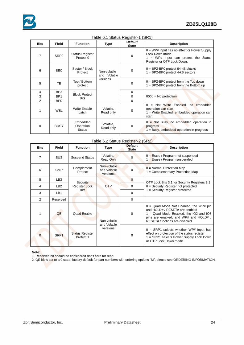
Table 6.1 Status Register-1 (SR1)
Bits Field Function Type Default State
Description
7 SRP0 Status Register
Protect 0
Non-volatile and Volatile versions
0
0 = WP# input has no effect or Power Supply Lock Down mode 1 = WP# input can protect the Status Register or OTP Lock Down.
6 SEC Sector / Block
Protect 0
0 = BP2-BP0 protect 64-kB blocks 1 = BP2-BP0 protect 4-kB sectors
5 TB Top / Bottom
protect 0
0 = BP2-BP0 protect from the Top down 1 = BP2-BP0 protect from the Bottom up
4 BP2 Block Protect
Bits
0
000b = No protection 3 BP1 0
2 BP0 0
1 WEL Write Enable
Latch Volatile,
Read only 0
0 = Not Write Enabled, no embedded operation can start 1 = Write Enabled, embedded operation can start
0 BUSY Embedded Operation
Status
Volatile, Read only
0 0 = Not Busy, no embedded operation in progress 1 = Busy, embedded operation in progress
Table 6.2 Status Register-2 (SR2)
Bits Field Function Type Default State
Description
7 SUS Suspend Status Volatile,
Read Only 0
0 = Erase / Program not suspended 1 = Erase / Program suspended
6 CMP Complement
Protect
Non-volatile and Volatile
versions 0
0 = Normal Protection Map 1 = Complementary Protection Map
5 LB3 Security
Register Lock Bits
OTP
0 OTP Lock Bits 3:1 for Security Registers 3:1 0 = Security Register not protected 1 = Security Register protected
4 LB2 0
3 LB1 0
2 Reserved 0
1 QE Quad Enable
Non-volatile and Volatile
versions
0
0 = Quad Mode Not Enabled, the WP# pin and HOLD# / RESET# are enabled 1 = Quad Mode Enabled, the IO2 and IO3 pins are enabled, and WP# and HOLD# / RESET# functions are disabled
0 SRP1 Status Register
Protect 1 0
0 = SRP1 selects whether WP# input has effect on protection of the status register 1 = SRP1 selects Power Supply Lock Down or OTP Lock Down mode
Note: 1. Reserved bit should be considered don't care for read. 2. QE bit is set to a 0 state, factory default for part numbers with ordering options ―M‖, please see ORDERING INFORMATION.

Zbit Semiconductor, Inc. Preliminary Datasheet 25
ZB25LQ128B
Table 6.3 Status Register-3 (SR3)
Bits Field Function Type Default State
Description
7 HRSW HOLD# or RESET# function
Non-volatile and volatile
versions
0
When HRSW=0, the pin acts as HOLD#; when HRSW=1, the pin acts as RESET#. HRSW functions are only available when QE=0.
6 DRV1
Output Driver Strength
1 The DRV1 & DRV0 bits are used to determine the output driver strength for the Read operations.
5 DRV0 1
4 HFM High Frequency
Mode Enable Bit
1 0 =Low Power Mode 1 =High Frequency Mode
3 Reserved Reserved N/A 0 N/A
2 WPS Write Protect
Selection
Non-volatile and Volatile
versions 0
When WPS=0, the device will use the combination of CMP, SEC, TB, BP[2:0] bits to protect a specific area of the memory array. When WPS=1, the device will utilize the Individual Block Locks to protect any individual sector or blocks.
1 Reserved Reserved N/A
0 N/A
0 0 N/A
6.2.1 BUSY
BUSY is a read only bit in the status register (SR1[0]) which is set to a ―1‖ state when the device is executing a Page Program, Sector Erase, Block Erase, Chip Erase or Write Status Register instruction. During this time the device will ignore further instructions except for the Read Status Register instruction (see tW, tPP, tSE, tBE, and tCE in AC Characteristics). When the program, erase or write status register instruction has completed, the BUSY bit will be cleared to a ―0‖ state indicating the device is ready for further instructions. 6.2.2 Write Enable Latch (WEL)
Write Enable Latch (WEL) is a read only bit in the status register (SR1[1]) which is set to a 1 after executing a Write Enable Instruction. The WEL status bit is cleared to a 0 when the device is written disabled. A write disable state occurs upon power-up or after any of the following instructions: Write Disable, Page Program, Sector Erase, Block Erase, Chip Erase and Write Status Register. 6.2.3 Block Protect Bits (BP2, BP1, BP0)
The Block Protect Bits (BP2, BP1, BP0) are non-volatile read / write bits in the Status Register (SR1[4:2])
that provide Write Protection control and status. Block Protect bits can be set using the Write Status Registers Command (see tW in Section 8.5). All, none or a portion of the memory array can be protected from Program and Erase commands (see Section 6.3.2, Block Protection Maps). The factory default setting for the Block Protection Bits is 0 (none of the array is protected.) 6.2.4 Top / Bottom Block Protect (TB)
The non-volatile Top / Bottom bit (TB SR1[5]) controls whether the Block Protect Bits (BP2, BP1, BP0) protect from the Top (TB=0) or the Bottom (TB=1) of the array as shown in Section 6.3.2, Block Protection Maps. The factory default setting is TB=0. The TB bit can be set with the Write Status Registers Command depending on the state of the SRP0, SRP1 and WEL bits. 6.2.5 Sector / Block Protect (SEC)
The non-volatile Sector / Block Protect bit (SEC SR1[6]) controls if the Block Protect Bits (BP2, BP1, BP0) protect either 4-kB Sectors (SEC=1) or 64-kB Blocks (SEC=0) of the array as shown in Section 6.3.2, Block Protection Maps. The default setting is SEC=0.
Zbit Semiconductor, Inc. Preliminary Datasheet 26
ZB25LQ128B
6.2.6 Complement Protect (CMP)
The Complement Protect bit (CMP SR2[6]) is a non-volatile read / write bit in the Status Register (SR2[6]). It is used in conjunction with SEC, TB, BP2, BP1 and BP0 bits to provide more flexibility for the array protection. Once CMP is set to 1, previous array protection set by SEC, TB, BP2, BP1 and BP0 will be reversed. For instance, when CMP=0, a top 4-kB sector can be protected while the rest of the array is not; when CMP=1, the top 4-kB sector will become unprotected while the rest of the array become read-only. Refer to Section 6.3.2, Block Protection Maps for details. The default setting is CMP=0. 6.2.7 The Status Register Protect (SRP1, SRP0)
The Status Register Protect bits (SRP1 and SRP0) are non-volatile read / write bits in the Status Register (SR2[0] and SR1[7]). The SRP bits control the method of write protection: software protection, hardware protection, power supply lock-down, or one time programmable (OTP) protection.
Table 6.4 Status Register Protect SRP1 SRP0 WP# Status Register Description
0 0 X Software Protection WP# pin has no control. SR1 and SR2 can be written to after a Write Enable command, WEL=1. [Factory Default]
0 1 0 Hardware Protected When WP# pin is low the SR1 and SR2 are locked and cannot be written.
0 1 1 Hardware
Unprotected When WP# pin is high SR1 and SR2 are unlocked and can be written to after a Write Enable command, WEL=1.
1 0 X Power Supply Lock
Down SR1 and SR2 are protected and cannot be written to again until the next power-down, power-up cycle.
(1)
1 1 X One Time Program (2)
SR1 and SR2 are permanently protected and cannot be written.
Notes:
1. When SRP1, SRP0 = (1, 0), a power-down, power-up, or Software Reset cycle will change SRP1, SRP0 to (0, 0) state. 2. The One-Time Program feature is available upon special order. Contact Zbit for details. 3. Busy, WEL, and SUS (SR1[1:0] and SR2[7]) are volatile read only status bits that are never affected by the Write Status
Registers command. 4. The non-volatile version of HRSW, DRV1, DRV0, HFM, CMP, QE, SRP1, SRP0, SEC, TB, and BP2-BP0 (SR3[7:4],
SR2[6,1,0] and SR1[6:2]) bits and the OTP LB3-LB1 bits are not writable when protected by the SRP bits and WP# as shown in the table. The non-volatile version of these Status Register bits is selected for writing when the Write Enable (06h) command precedes the Write Status Registers (01h/31h/11h) command.
5. The volatile version of HRSW, DRV1, DRV0, HFM, CMP, QE, SRP1, SRP0, SEC, TB, and BP2-BP0 (SR3[7:4], SR2[6,1,0] and SR1[6:2]) bits are not writable when protected by the SRP bits and WP# as shown in the table. The volatile version of these Status Register bits is selected for writing when the Write Enable for volatile Status Register (50h) command precedes the Write Status Registers (01h/31h/11h) command. There is no volatile version of the LB3-LB1 bits and these bits are not affected by a volatile Write Status Registers command.
6.2.8 Erase / Program Suspend Status (SUS)
The Suspend Status bit is a read only bit in the status register (SR2[7]) that is set to 1 after executing an Erase / Program Suspend (75h) command. The SUS status bit is cleared to 0 by Erase / Program Resume (7Ah) command as well as a power-down, power-up cycle. 6.2.9 Security Register Lock Bits (LB3, LB2, LB1)
The Security Register Lock Bits (LB3, LB2, LB1) are non-volatile One Time Program (OTP) bits in Status Register (SR2[5:3]) that provide the write protect control and status to the Security Registers. The default state of LB[3:1] is 0, Security Registers 1 to 3 are unlocked. LB[3:1] can be set to 1 individually using the Write Status Registers command. LB[3:1] are One Time Programmable (OTP), once it‘s set to 1, the corresponding 1024-byte Security Register will become read-only permanently.
6.2.10 Quad Enable (QE)
The Quad Enable (QE) bit is a non-volatile read / write bit in the Status Register (SR2[1]) that allows Quad SPI operation. When the QE bit is set to a 0 state (factory default), the WP# pin and HOLD# / RESET#

Zbit Semiconductor, Inc. Preliminary Datasheet 27
ZB25LQ128B
are enabled. When the QE bit is set to a 1, the Quad IO2 and IO3 pins are enabled, and WP# and HOLD# / RESET# functions are disabled. Note: (1) If the WP# or HOLD# / RESET# pins are tied directly to the power supply or ground during standard SPI or Dual SPI operation, the QE bit should never be set to a 1. (2) QE bit is set to a 0 state, factory default for part numbers with ordering options ―M‖, please see ORDERING INFORMATION.
6.2.11 HOLD# or RESET# Pin Function (HRSW)
The HRSW bit is used to determine whether HOLD# or RESET# function should be implemented on the
hardware pin for 8-pin packages. When HRSW=0, the pin acts as #HOLD; when HRSW=1, the pin acts as RESET#. However, HOLD# or RESET# functions are only available when QE=0. If QE is set to 1, the HOLD# and RESET# functions are disabled, the pin acts as a dedicated data I/O pin.
6.2.12 Output Driver Strength (DRV1, DRV0)
The DRV1 & DRV0 bits are used to determine the output driver strength for the Read operations.
DRV1, DRV0 Driver Strength
0, 0 50%
0, 1 25%
1, 0 75%
1, 1 100%
6.2.13 High Frequency Mode Enable Bit (HFM)
The HFM bit is used to determine whether the device is in High Frequency Mode. When HFM bit sets to 1, it means the device is in High Frequency Mode, when HFM bit sets to 0, it means the device is in Low Power Mode. After the HFM is set to 0, the device will maintain a much lower standby current (ICC8) than standard SPI operation.
6.2.14 Write Protect Selection (WPS)
The WPS bit is used to select which Write Protect scheme should be used. When WPS=0, the device will use the combination of CMP, SEC, TB, BP[2:0] bits to protect a specific area of the memory array. When WPS=1, the device will utilize the Individual Block Locks to protect any individual sector or blocks. The default value for all Individual Block Lock bits is 1 upon device power on or after reset.
6.3. Write Protection
Applications that use non-volatile memory must take into consideration the possibility of noise and other
adverse system conditions that may compromise data integrity. To address this concern the ZB25LQ128B provides the following data protection mechanisms:
6.3.1 Write Protect Features
Device resets when VCC is below threshold
Time delay write disable after Power-Up
Write enable / disable commands and automatic write disable after erase or program
Command length protection - All commands that Write, Program or Erase must complete on a byte boundary (CS# driven high after
a full 8 bits have been clocked) otherwise the command will be ignored.
Software and Hardware write protection using Status Register control

Zbit Semiconductor, Inc. Preliminary Datasheet 28
ZB25LQ128B
- WP# input protection - Lock Down write protection until next power-up or Software Reset - One-Time Program (OTP) write protection
Write Protection using the Deep Power-Down command
Upon power-up or at power-down, the ZB25LQ128B will maintain a reset condition while VCC is below the threshold value of VWI, (see Figure 8.1). While reset, all operations are disabled and no commands are recognized. During power-up and after the VCC voltage exceeds VWI, all program and erase related commands are further disabled for a time delay of tPUW. This includes the Write Enable, Page Program, Sector Erase, Block Erase, Chip Erase and the Write Status Registers commands.
After power-up the device is automatically placed in a write-disabled state with the Status Register Write
Enable Latch (WEL) set to a 0. A Write Enable command must be issued before a Page Program, Sector Erase, Block Erase, Chip Erase or Write Status Registers command will be accepted. After completing a program, erase or write command the Write Enable Latch (WEL) is automatically cleared to a write-disabled state of 0.
Software controlled main flash array write protection is facilitated using the Write Status Registers
command to write the Status Register (SR1,SR2) and Block Protect (SEC, TB, BP2, BP1 and BP0) bits. The BP method allows a portion as small as 4-kB sector or the entire memory array to be configured as
read only. Used in conjunction with the Write Protect (WP#) pin, changes to the Status Register can be enabled or disabled under hardware control. See the Table 6.4 for further information.
Additionally, the Deep Power-Down (DPD) command offers an alternative means of data protection as all
commands are ignored during the DPD state, except for the Release from Deep-Power-Down (RES ABh) command. Thus, preventing any program or erase during the DPD state.
Zbit Semiconductor, Inc. Preliminary Datasheet 29
ZB25LQ128B
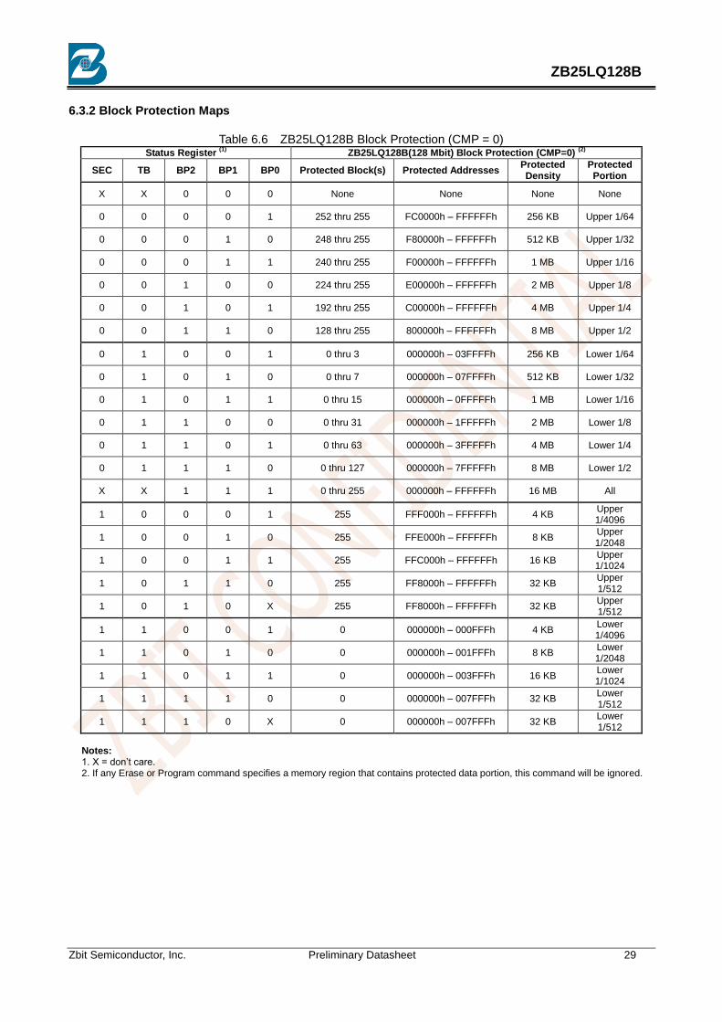
6.3.2 Block Protection Maps
Table 6.6 ZB25LQ128B Block Protection (CMP = 0)
Status Register (1)
ZB25LQ128B(128 Mbit) Block Protection (CMP=0) (2)
SEC TB BP2 BP1 BP0 Protected Block(s) Protected Addresses Protected Density
Protected Portion
X X 0 0 0 None None None None
0 0 0 0 1 252 thru 255 FC0000h – FFFFFFh 256 KB Upper 1/64
0 0 0 1 0 248 thru 255 F80000h – FFFFFFh 512 KB Upper 1/32
0 0 0 1 1 240 thru 255 F00000h – FFFFFFh 1 MB Upper 1/16
0 0 1 0 0 224 thru 255 E00000h – FFFFFFh 2 MB Upper 1/8
0 0 1 0 1 192 thru 255 C00000h – FFFFFFh 4 MB Upper 1/4
0 0 1 1 0 128 thru 255 800000h – FFFFFFh 8 MB Upper 1/2
0 1 0 0 1 0 thru 3 000000h – 03FFFFh 256 KB Lower 1/64
0 1 0 1 0 0 thru 7 000000h – 07FFFFh 512 KB Lower 1/32
0 1 0 1 1 0 thru 15 000000h – 0FFFFFh 1 MB Lower 1/16
0 1 1 0 0 0 thru 31 000000h – 1FFFFFh 2 MB Lower 1/8
0 1 1 0 1 0 thru 63 000000h – 3FFFFFh 4 MB Lower 1/4
0 1 1 1 0 0 thru 127 000000h – 7FFFFFh 8 MB Lower 1/2
X X 1 1 1 0 thru 255 000000h – FFFFFFh 16 MB All
1 0 0 0 1 255 FFF000h – FFFFFFh 4 KB Upper 1/4096
1 0 0 1 0 255 FFE000h – FFFFFFh 8 KB Upper 1/2048
1 0 0 1 1 255 FFC000h – FFFFFFh 16 KB Upper 1/1024
1 0 1 1 0 255 FF8000h – FFFFFFh 32 KB Upper 1/512
1 0 1 0 X 255 FF8000h – FFFFFFh 32 KB Upper 1/512
1 1 0 0 1 0 000000h – 000FFFh 4 KB Lower 1/4096
1 1 0 1 0 0 000000h – 001FFFh 8 KB Lower 1/2048
1 1 0 1 1 0 000000h – 003FFFh 16 KB Lower 1/1024
1 1 1 1 0 0 000000h – 007FFFh 32 KB Lower 1/512
1 1 1 0 X 0 000000h – 007FFFh 32 KB Lower 1/512
Notes: 1. X = don‘t care. 2. If any Erase or Program command specifies a memory region that contains protected data portion, this command will be ignored.
Zbit Semiconductor, Inc. Preliminary Datasheet 30
ZB25LQ128B
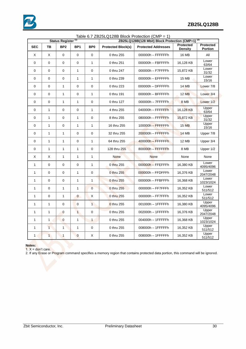
Table 6.7 ZB25LQ128B Block Protection (CMP = 1) Status Register
(1) ZB25LQ128B(128 Mbit) Block Protection (CMP=1)
(2)
SEC TB BP2 BP1 BP0 Protected Block(s) Protected Addresses Protected Density
Protected Portion
X X 0 0 0 0 thru 255 000000h – FFFFFFh 16 MB All
0 0 0 0 1 0 thru 251 000000h – FBFFFFh 16,128 KB Lower 63/64
0 0 0 1 0 0 thru 247 000000h – F7FFFFh 15,872 KB Lower 31/32
0 0 0 1 1 0 thru 239 000000h – EFFFFFh 15 MB Lower 15/16
0 0 1 0 0 0 thru 223 000000h – DFFFFFh 14 MB Lower 7/8
0 0 1 0 1 0 thru 191 000000h – BFFFFFh 12 MB Lower 3/4
0 0 1 1 0 0 thru 127 000000h – 7FFFFFh 8 MB Lower 1/2
0 1 0 0 1 4 thru 255 040000h – FFFFFFh 16,128 KB Upper 63/64
0 1 0 1 0 8 thru 255 080000h – FFFFFFh 15,872 KB Upper 31/32
0 1 0 1 1 16 thru 255 100000h – FFFFFFh 15 MB Upper 15/16
0 1 1 0 0 32 thru 255 200000h – FFFFFFh 14 MB Upper 7/8
0 1 1 0 1 64 thru 255 400000h – FFFFFFh 12 MB Upper 3/4
0 1 1 1 0 128 thru 255 800000h – FFFFFFh 8 MB Upper 1/2
X X 1 1 1 None None None None
1 0 0 0 1 0 thru 255 000000h – FFEFFFh 16,380 KB Lower
4095/4096
1 0 0 1 0 0 thru 255 000000h – FFDFFFh 16,376 KB Lower
2047/2048
1 0 0 1 1 0 thru 255 000000h – FFBFFFh 16,368 KB Lower
1023/1024
1 0 1 1 0 0 thru 255 000000h – FF7FFFh 16,352 KB Lower
511/512
1 0 1 0 X 0 thru 255 000000h – FF7FFFh 16,352 KB Lower
511/512
1 1 0 0 1 0 thru 255 001000h – 1FFFFFh 16,380 KB Upper
4095/4096
1 1 0 1 0 0 thru 255 002000h – 1FFFFFh 16,376 KB Upper
2047/2048
1 1 0 1 1 0 thru 255 004000h – 1FFFFFh 16,368 KB Upper
1023/1024
1 1 1 1 0 0 thru 255 008000h – 1FFFFFh 16,352 KB Upper
511/512
1 1 1 0 X 0 thru 255 008000h – 1FFFFFh 16,352 KB Upper
511/512
Notes: 1. X = don‘t care. 2. If any Erase or Program command specifies a memory region that contains protected data portion, this command will be ignored.

Zbit Semiconductor, Inc. Preliminary Datasheet 31
ZB25LQ128B
6.3.3 Individual Block Memory Protection (WPS=1)
Sector 0(4KB)
Block 254 (64KB)
Sector 1(4KB)
Sector 14(4KB)
Sector 15(4KB)
...…
...
Sector 15(4KB)
Blo
ck 0
(6
4K
B)
Sector 14(4KB)
Sector 1(4KB)
Sector 0(4KB)
...
Block 1 (64KB)
Blo
ck 2
55
(6
4K
B)
Individual Block Locks:
32 Sectors (Top/
Bottom) 254 Blocks
Individual Block Lock:
36h + Address
Individual Block Unlock:
39h + Address
Read Block Unlock:
3Dh + Address
Global Block lock:
7Eh
Global Block Unlock:
98h
Figure 6.2 Individual Block/Sector Locks
Notes: 1. Individual Block/Sector protection is only valid when WPS=1. 2. All individual block/sector lock bits are set to 1 by default after power up, all memory array is protected.

Zbit Semiconductor, Inc. Preliminary Datasheet 32
ZB25LQ128B
6.4. Page Program
To program one data byte, two instructions are required: Write Enable (WREN), which is one byte, and a
Page Program (PP) sequence, which consists of four bytes plus data. This is followed by the internal Program cycle (of duration tPP). To spread this overhead, the Page Program (PP) instruction allows up to 256 bytes to be programmed at a time (changing bits from 1 to 0), provided that they lie in consecutive addresses on the same page of memory.
6.5. Sector Erase, Block Erase and Chip Erase
The Page Program (PP) instruction allows bits to be reset from 1 to 0. Before this can be applied, the
bytes of memory need to be erased to all 1s (FFh). This can be achieved a sector at a time, using the Sector Erase (SE) instruction, a block at a time using the Block Erase (BE) instruction or throughout the entire memory, using the Chip Erase (CE) instruction. This starts an internal Erase cycle (of duration tSE tBE or tCE). The Erase instruction must be preceded by a Write Enable (WREN) instruction.
6.6. Polling during a Write, Program or Erase Cycle
A further improvement in the time to Write Status Register (WRSR), Program (PP) or Erase (SE, BE or
CE) can be achieved by not waiting for the worst case delay (tW, tPP, tSE, tBE or tCE). The Write In Progress (WIP) bit is provided in the Status Register so that the application program can monitor its value, polling it to establish when the previous Write cycle, Program cycle or Erase cycle is complete.
6.7. Active Power, Stand-by Power and Deep Power-Down Modes
When Chip Select (CS#) is Low, the device is enabled, and in the Active Power mode. When Chip Select
(CS#) is High, the device is disabled, but could remain in the Active Power mode until all internal cycles have completed (Program, Erase, Write Status Register). The device then goes into the Standby Power mode. The device consumption drops to ICC1.
The Deep Power-down mode is entered when the specific instruction (the Enter Deep Power-down Mode (DP) instruction) is executed. The device consumption drops further to ICC2. The device remains in this mode until another specific instruction (the Release from Deep Power-down Mode and Read Device ID (RDI) instruction) is executed.
All other instructions are ignored while the device is in the Deep Power-down mode. This can be used as an extra software protection mechanism, when the device is not in active use, to protect the device from inadvertent Program or Erase instructions.

Zbit Semiconductor, Inc. Preliminary Datasheet 33
ZB25LQ128B
7. INSTRUCTIONS
The instruction set of the ZB25LQ128B consists of forty basic instructions that are fully controlled through the SPI bus. Instructions are initiated with the falling edge of Chip Select (CS#). The first byte of data clocked into the DI input provides the instruction code. Data on the DI input is sampled on the rising edge of clock with most significant bit (MSB) first.
The QPI instruction set of the ZB25LQ128B consists of 32 basic instructions that are fully controlled through the SPI bus (see Instruction Set Table 7.5). Instructions are initiated with the falling edge of Chip Select (CS#). The first byte of data clocked through IO[3:0] pins provides the instruction code. Data on all four IO pins are sampled on the rising edge of clock with most significant bit (MSB) first. All QPI instructions, addresses, data and dummy bytes are using all four IO pins to transfer every byte of data with every two serial clocks (CLK).
Instructions vary in length from a single byte to several bytes and may be followed by address bytes, data bytes, dummy bytes (don‘t care), and in some cases, a combination. Instructions are completed with the rising edge of edge CS#. Clock relative timing diagrams for each instruction are included in figures 7.1 through 7.43. All read instructions can be completed after any clocked bit. However, all instructions that Write, Program or Erase must complete on a byte boundary (CS driven high after a full 8-bits have been clocked) otherwise the instruction will be ignored. This feature further protects the device from inadvertent writes. Additionally, while the memory is being programmed or erased, or when the Status Register is being written, all instructions except for Read Status Register and Erase/Program Suspend will be ignored until the program or erase cycle completes.

Zbit Semiconductor, Inc. Preliminary Datasheet 34
ZB25LQ128B
Table 7.1 Command Set (Configuration, Status, Erase, Program Instructions
(1), SPI Mode)
Command Name BYTE 1
(Instruction) BYTE 2 BYTE 3 BYTE 4 BYTE 5 BYTE 6
Read Status Register-1 05h SR1[7:0](2)
Read Status Register-2 35h SR2[7:0](2)
Read Status Register-3 15h SR3[7:0](2)
Write Enable 06h
Write Enable for Volatile Status Register
50h
Write Disable 04h
Write Status Registers-1 01h SR1[7:0](5)
SR2[7:0] SR3[7:0]
Write Status Registers-2 31h SR2[7:0]
Write Status Registers-3 11h SR3[7:0]
Set Burst with Wrap 77h xxh xxh xxh W[7:0](3)
Global Block Lock 7Eh
Global Block Unlock 98h
Read Block Lock 3Dh A23—A16 A15—A8 A7—A0 L7—L0
Individual Block Lock 36h A23—A16 A15—A8 A7—A0
Individual Block Unlock 39h A23—A16 A15—A8 A7—A0
Page Program 02h A23—A16 A15—A8 A7—A0 D7—D0
Quad Page Program 32h A23—A16 A15—A8 A7—A0 D7—D0(4)
Sector Erase (4 KB) 20h A23—A16 A15—A8 A7—A0
Block Erase (32 KB) 52h A23—A16 A15—A8 A7—A0
Block Erase (64 KB) D8h A23—A16 A15—A8 A7—A0
Chip Erase C7h/60h
Erase/Program Suspend
75h
Erase/Program Resume 7Ah
Enter QPI Mode 38h
Enable Reset 66h
Reset Device 99h
Notes: 1. Data bytes are shifted with Most Significant Bit first. Byte fields with data in parenthesis ―()‖ indicate data being read from the device on the DO pin. 2. Status Register contents will repeat continuously until CS# terminates the command. 3. Set Burst with Wrap Input format. IO0 = x, x, x, x, x, x, W4, x IO1 = x, x, x, x, x, x, W5, x IO2 = x, x, x, x, x, x, W6 x IO3 = x, x, x, x, x, x, x,x 4. Quad Page Program Input Data: IO0 =(D4,D0,...) IO1 = ( D5,D1,...) IO2 = ( D6,D2,...) IO3 =( D7,D3,...) 5. The 01h command could continuously write up to three bytes to registers SR1, SR2, SR3.

Zbit Semiconductor, Inc. Preliminary Datasheet 35
ZB25LQ128B
Table 7.2 Command Set (Read Instructions
(1), SPI Mode)
Command Name BYTE 1
(Instruction) BYTE 2 BYTE 3 BYTE 4 BYTE 5 BYTE 6
Read Data 03h A23—A16 A15—A8 A7—A0 (D7—D0,…)
Fast Read 0Bh A23—A16 A15—A8 A7—A0 dummy (D7—D0,…)
Fast Read Dual Output
3Bh A23—A16 A15—A8 A7—A0 dummy (D7—D0,…)(1)
Fast Read Quad Output
6Bh A23—A16 A15—A8 A7—A0 dummy (D7—D0,…)(3)
Fast Read Dual I/O BBh A23—A8(2)
A7—A0,M7—M0
(2)
(D7—D0,…)(1)
Fast Read Quad I/O
EBh A23—A0,M7—M0
(4)
(x,x,x,x,D7—D0,...)
(D7—D0,…)(3)
QUAD I/O WORD FAST READ
(5)
E7H A23—A0,M7—M0
(4)
(x,x,D7—D0,...)
(D7—D0,…)(3)
Octal Word Read Quad I/O
(5)
E3h A23—A0,M7—M0
(4)
(D7—D0,…)(
3)
(D7—D0,…)(3)
Notes: 1. Dual Output data IO0 = (D6, D4, D2, D0) IO1 = (D7, D5, D3, D1) 2. Dual Input Address IO0 = A22, A20, A18, A16, A14, A12, A10, A8, A6, A4, A2, A0, M6, M4, M2, M0 IO1 = A23, A21, A19, A17, A15, A13, A11, A9, A7, A5, A3, A1, M7, M5, M3, M1 3. Quad Output Data IO0 = (D4, D0, …..) IO1 = (D5, D1, …..) IO2 = (D6, D2, …..) IO3 = (D7, D3, …..) 4. Quad Input Address IO0 = A20, A16, A12, A8, A4, A0, M4, M0 IO1 = A21, A17, A13, A9, A5, A1, M5, M1 IO2 = A22, A18, A14, A10, A6, A2, M6, M2 IO3 = A23, A19, A15, A11, A7, A3, M7, M3 5. For Word Read Quad I/O, the lowest address bit must be 0. (A0 = 0),and for Octal Word Read Quad I/O, the lowest four address bits must be 0. (A3, A2, A1, A0 = 0)

Zbit Semiconductor, Inc. Preliminary Datasheet 36
ZB25LQ128B
Table 7.3 Command Set (Read ID, OTP Instructions
(1), SPI Mode)
Command Name
BYTE 1 (Instruction)
BYTE 2 BYTE 3 BYTE 4 BYTE 5 BYTE 6
Deep Power-down
B9h
Release Power down / Device ID
ABh dummy dummy dummy Device ID(1)
Manufacturer/ Device ID
(2)
90h dummy dummy 00h Manufacturer Device ID
Manufacturer/ Device ID by Dual I/O
92h A23—A8 A7—A0,M[7:0] (MF[7:0],ID[7:0])
Manufacturer/ Device ID by Quad I/O
94h A23—A0,M[7:0] XXXX,(MF[7:0],ID[7:0]) (MF[7:0],ID[7:0]...)
JEDEC ID 9Fh Manufacturer Memory Type Capacity
Read SFDP Register
5Ah 00h 00h A7—A0 dummy (D7—D0,…)
Read Security Registers
(3)
48h A23—A16 A15—A8 A7—A0 dummy (D7—D0,…)
Erase Security Registers
(3)
44h A23—A16 A15—A8 A7—A0
Program Security Registers
(3)
42h A23—A16 A15—A8 A7—A0 D7—D0,…
Read Unique ID
4Bh dummy dummy dummy dummy (ID127-ID0)
Notes: 1. The Device ID will repeat continuously until CS# terminates the command. 2. Legacy Device Identification Commands on page 53 for Device ID information. The 90h instruction is followed by an address. Address = 0 selects Manufacturer ID as the first returned data as shown in the table. Address = 1 selects Device ID as the first returned data followed by Manufacturer ID. 3. Security Register Address: Security Register 1: A23-16 = 00h; A15-10 = 000100b; A9-0 = byte address Security Register 2: A23-16 = 00h; A15-10 = 001000b; A9-0 = byte address Security Register 3: A23-16 = 00h; A15-10 = 001100b; A9-0 = byte address
Table 7.4
(1) Manufacturer and Device Identification(ZB25LQ128B)
OP Code Data1 Data2 Data3
ABh Device ID = 17h - -
90h/92h/94h Manufacturer ID = 5E Device ID = 17h -
9Fh/AFh Manufacturer ID = 5E Memory Type =50h Capacity = 18h
Notes: (1) Please contact sales for more information

Zbit Semiconductor, Inc. Preliminary Datasheet 37
ZB25LQ128B
Table 7.5 Command Set (QPI Instructions
(1), QPI Mode)
Command Name BYTE 1
(Instruction) BYTE 2 BYTE 3 BYTE 4 BYTE 5 BYTE 6
Clock Number (0, 1) (2, 3) (4, 5) (6, 7) (8, 9) (10, 11)
Write Enable 06h
Write Enable for Volatile Status Register
50h
Write Disable 04h
Read Status Register-1 05h (S7-S0)(1)
Write Status Register-1(3)
01h (S7-S0)(3)
(S15-S8) (S23-S16)
Read Status Register-2 35h (S15-S8)(1)
Write Status Register-2 31h (S15-S8)
Read Status Register-3 15h (S23-S16)(1)
Write Status Register-3 11h (S23-S16)
Global Block Lock 7Eh
Global Block Unlock 98h
Read Block Lock 3Dh A23—A16 A15—A8 A7—A0 L7—L0
Individual Block Lock 36h A23—A16 A15—A8 A7—A0
Individual Block Unlock 39h A23—A16 A15—A8 A7—A0
Chip Erase C7h/60h
Erase / Program Suspend 75h
Erase / Program Resume 7Ah
Deep Power-down B9h
Set Read Parameters C0h P7-P0
Release Power down / ID ABh Dummy Dummy Dummy (ID7-ID0)(1)
Manufacturer/Device ID 90h Dummy Dummy 00h (MF7-MF0) (ID7-ID0)
JEDEC ID 9Fh/AFh (MF7-MF0) (ID15-ID8) (ID7-ID0)
Exit QPI Mode FFh
Enable Reset 66h
Reset Device 99h
Page Program 02h A23-A16 A15-A8 A7-A0 D7-D0(4)
D7-D0(2)
Sector Erase (4KB) 20h A23-A16 A15-A8 A7-A0
Block Erase (32KB) 52h A23-A16 A15-A8 A7-A0
Block Erase (64KB) D8h A23-A16 A15-A8 A7-A0
Fast Read 0Bh A23-A16 A15-A8 A7-A0 Dummy(5)
D7-D0
Burst Read with Wrap(6)
0Ch A23-A16 A15-A8 A7-A0 Dummy(5)
D7-D0
Fast Read Quad I/O EBh A23-A16 A15-A8 A7-A0 M7-M0(5)
D7-D0
Notes: 1. The Status Register contents and Device ID will repeat continuously until CS# terminates the instruction. 2. At least one byte of data input is required for Page Program, Quad Page Program and Program Security Registers, up to 1024 bytes of data input. If more than 1024 bytes of data are sent to the device, the addressing will wrap to the beginning of the page and overwrite previously sent data. 3. Write Status Register-1 (01h) can also be used to program Status Register-1&2&3, see section 7.1.5. 4. Quad SPI data input/output format: IO0 = (D4, D0, …..) IO1 = (D5, D1, …..) IO2 = (D6, D2, …..) IO3 = (D7, D3, …..) 5. The number of dummy clocks for QPI Fast Read, QPI Fast Read Quad I/O & QPI Burst Read with Wrap is controlled by read parameter P7 – P4. 6. The wrap around length for QPI Burst Read with Wrap is controlled by read parameter P3 – P0.

Zbit Semiconductor, Inc. Preliminary Datasheet 38
ZB25LQ128B
7.1 Configuration and Status Commands
7.1.1 Read Status Register (05h/35h/15h) The Read Status Register commands allow the 8-bit Status Registers to be read. The command is
entered by driving CS# low and shifting the instruction code ―05h‖ for Status Register-1, ―35h‖ for Status Register-2, ―15h‖ for Status Register-3 into the DI pin on the rising edge of CLK. The Status Register bits are then shifted out on the DO pin at the falling edge of CLK with most significant bit (MSB) first as shown in Figure 7.1. The Status Register bits are shown in Section 6.2, Status Registers.
The Read Status Register-1 (05h) command may be used at any time, even during a Program, Erase, or Write Status Registers cycle. This allows the BUSY status bit to be checked to determine when the operation is complete and if the device can accept another command.
DI
DO
0
CLK
CS#
1 2 3 4 5 6 7 8 9 10 11 12 13 14 15 16 17 18 19 20 21 22 23
05h/35h/15h
S7~S0 out S7~S0 out
Instruction Status Updated Status
Mode 0
Mode 3
Mode 0
Mode 3
Figure 7.1a Read Status Register Instruction(SPI Mode)
IO0
IO1
0
CLK
CS#
1
4 0
5 1
6 2
7 3
IO2
IO3
Instruction
05h/35h/15h
Mode 0
Mode 3 2 3 4 5
S4 S0
S5 S1
S6 S2
S7 S3
S4 S0
S5 S1
S6 S2
S7 S3
SR-1/2/3
out
SR-1/2/3
out
S4
S5
S6
S7
Figure 7.1b Read Status Register Instruction(QPI Mode)
7.1.2 Write Enable (06h)
The Write Enable instruction (Figure 7.2) sets the Write Enable Latch (WEL) bit in the Status Register to a
1. The WEL bit must be set prior to every Page Program, Sector Erase, Block Erase, Chip Erase and Write Status Register instruction. The Write Enable instruction is entered by driving CS# low, shifting the instruction code ―06h‖ into the Data Input (DI) pin on the rising edge of CLK, and then driving CS# high.
IO0
IO1
0
CLK
CS#
1
4 0
5 1
6 2
7 3
IO2
IO3
Instruction
06h
Mode 0
Mode 3
Mode 0
Mode 3
DI
DO
0
CLK
CS#
1 2 3 4 5 6 7
06h
Instruction
Mode 0
Mode 3
Mode 0
Mode 3
Figure 7.2 Write Enable Instruction (SPI or QPI Mode)
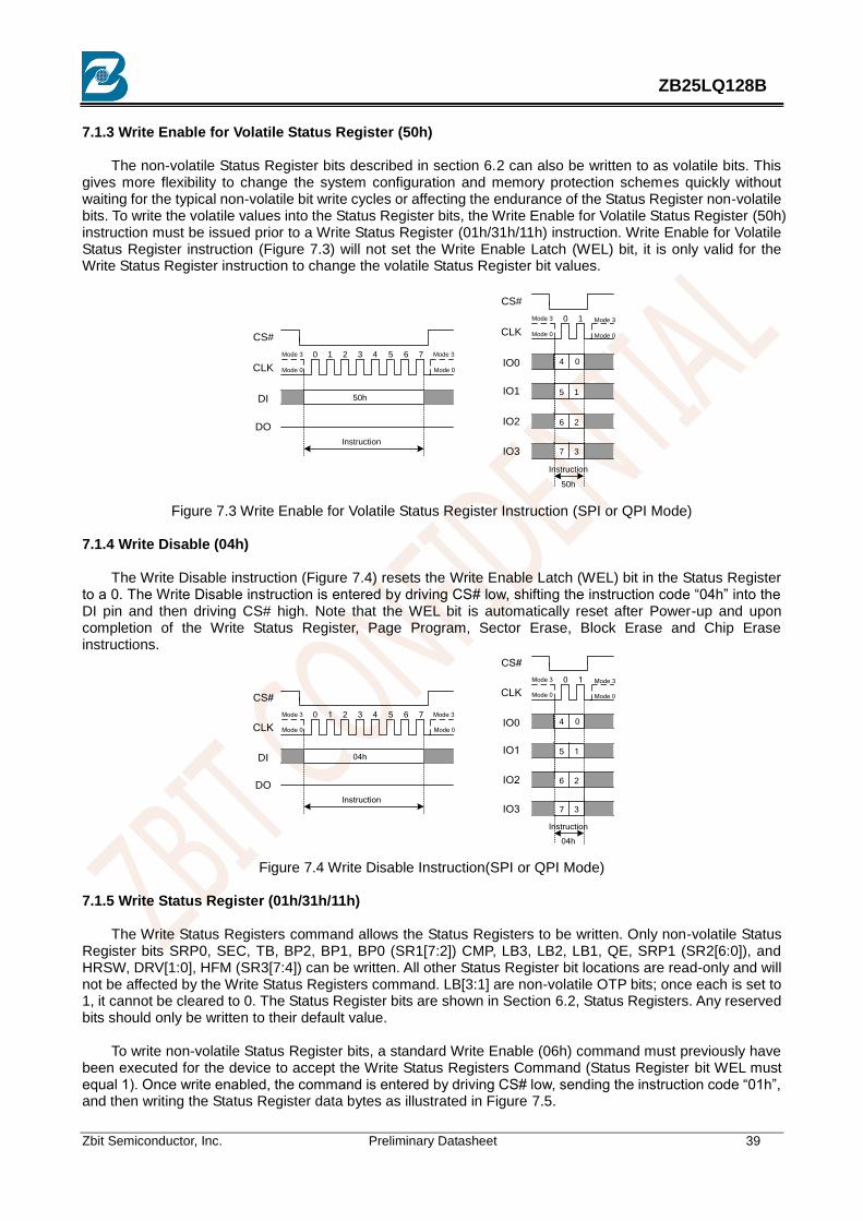
Zbit Semiconductor, Inc. Preliminary Datasheet 39
ZB25LQ128B
7.1.3 Write Enable for Volatile Status Register (50h)
The non-volatile Status Register bits described in section 6.2 can also be written to as volatile bits. This
gives more flexibility to change the system configuration and memory protection schemes quickly without waiting for the typical non-volatile bit write cycles or affecting the endurance of the Status Register non-volatile bits. To write the volatile values into the Status Register bits, the Write Enable for Volatile Status Register (50h) instruction must be issued prior to a Write Status Register (01h/31h/11h) instruction. Write Enable for Volatile Status Register instruction (Figure 7.3) will not set the Write Enable Latch (WEL) bit, it is only valid for the Write Status Register instruction to change the volatile Status Register bit values.
DI
DO
0
CLK
CS#
1 2 3 4 5 6 7
50h
Instruction
Mode 0
Mode 3
Mode 0
Mode 3
IO0
IO1
0
CLK
CS#
1
4 0
5 1
6 2
7 3
IO2
IO3
Instruction
50h
Mode 0
Mode 3
Mode 0
Mode 3
Figure 7.3 Write Enable for Volatile Status Register Instruction (SPI or QPI Mode)
7.1.4 Write Disable (04h)
The Write Disable instruction (Figure 7.4) resets the Write Enable Latch (WEL) bit in the Status Register
to a 0. The Write Disable instruction is entered by driving CS# low, shifting the instruction code ―04h‖ into the DI pin and then driving CS# high. Note that the WEL bit is automatically reset after Power-up and upon completion of the Write Status Register, Page Program, Sector Erase, Block Erase and Chip Erase instructions.
DI
DO
0
CLK
CS#
1 2 3 4 5 6 7
04h
Instruction
Mode 0
Mode 3
Mode 0
Mode 3
IO0
IO1
0
CLK
CS#
1
4 0
5 1
6 2
7 3
IO2
IO3
Instruction
04h
Mode 0
Mode 3
Mode 0
Mode 3
Figure 7.4 Write Disable Instruction(SPI or QPI Mode)
7.1.5 Write Status Register (01h/31h/11h)
The Write Status Registers command allows the Status Registers to be written. Only non-volatile Status
Register bits SRP0, SEC, TB, BP2, BP1, BP0 (SR1[7:2]) CMP, LB3, LB2, LB1, QE, SRP1 (SR2[6:0]), and HRSW, DRV[1:0], HFM (SR3[7:4]) can be written. All other Status Register bit locations are read-only and will not be affected by the Write Status Registers command. LB[3:1] are non-volatile OTP bits; once each is set to 1, it cannot be cleared to 0. The Status Register bits are shown in Section 6.2, Status Registers. Any reserved bits should only be written to their default value.
To write non-volatile Status Register bits, a standard Write Enable (06h) command must previously have been executed for the device to accept the Write Status Registers Command (Status Register bit WEL must equal 1). Once write enabled, the command is entered by driving CS# low, sending the instruction code ―01h‖, and then writing the Status Register data bytes as illustrated in Figure 7.5.

Zbit Semiconductor, Inc. Preliminary Datasheet 40
ZB25LQ128B
To write volatile Status Register bits, a Write Enable for Volatile Status Register (50h) command must
have been executed prior to the Write Status Registers command (Status Register bit WEL remains 0). However, SRP1 and LB3, LB2, LB1 cannot be changed because of the OTP protection for these bits. Upon power-off, the volatile Status Register bit values will be lost, and the non-volatile Status Register bit values will be restored when power on again.
CS# must be driven high after the 8th, 16th or 24th bit of the data byte has been latched in. If not, the Write Status Register(WRSR) command is not executed.
During non-volatile Status Register write operation (06h combined with 01h/31h/11h), after CS# is driven high, the self-timed Write Status Register cycle will commence for a time duration of tW (See AC Characteristics). While the Write Status Register cycle is in progress, the Read Status Register instruction may still be accessed to check the status of the BUSY bit. The BUSY bit is a 1 during the Write Status Register cycle and a 0 when the cycle is finished and ready to accept other instructions again. After the Write Status Register cycle has finished, the Write Enable Latch (WEL) bit in the Status Register will be cleared to 0.
During volatile Status Register write operation (50h combined with 01h/31h/11h), after CS# is driven high,
the Status Register bits will be refreshed to the new values within the time period of tSHSL2 (See AC Characteristics). BUSY bit will remain 0 during the Status Register bit refresh period.
DI
DO
0
CLK
CS#
1 2 3 4 5 6 7 8 9 10 11 12 13 14 15
01h/31h/11h
Instruction Input Status Register
S7~S0 in
Mode 0
Mode 3
Mode 0
Mode 3
Figure 7.5a Write Status Register Instruction(SPI Mode)
IO0
IO1
0
CLK
CS#
1
4 0
5 1
6 2
7 3
IO2
IO3
Instruction
01h/31h/11h
Mode 0
Mode 3 2 3
S4 S0
S5 S1
S6 S2
S7 S3
SR-1/2/3
in
Mode 0
Mode 3
Figure 7.5b Write Status Register Instruction(QPI Mode)
7.2 Program and Erase Commands
7.2.1 Page Program (PP) (02h)
The Page Program instruction allows up to 256 bytes of data to be programmed at previously erased to all 1s (FFh) memory locations. A Write Enable instruction must be executed before the device will accept the Page Program Instruction (Status Register bit WEL must equal 1). The instruction is initiated by driving the CS# pin low then shifting the instruction code ―02h‖ followed by a 24-bit address (A23-A0) and at least one data byte, into the DI pin. The CS# pin must be held low for the entire length of the instruction while data is being sent to the device. The Page Program instruction sequence is shown in Figure 7.6.
If an entire 256 byte page is to be programmed, the last address byte (the 8 least significant address bits)
should be set to 0. If the last address byte is not zero, and the number of clocks exceeds the remaining page length, the addressing will wrap to the beginning of the page. In some cases, less than 256 bytes (a partial

Zbit Semiconductor, Inc. Preliminary Datasheet 41
ZB25LQ128B
page) can be programmed without having any effect on other bytes within the same page. One condition to perform a partial page program is that the number of clocks cannot exceed the remaining page length. If more than 256 bytes are sent to the device the addressing will wrap to the beginning of the page and overwrite previously sent data.
As with the write and erase instructions, the CS# pin must be driven high after the eighth bit of the last byte has been latched. If this is not done the Page Program instruction will not be executed. After CS# is driven high, the self-timed Page Program instruction will commence for a time duration of tpp (See AC Characteristics). While the Page Program cycle is in progress, the Read Status Register instruction may still be accessed for checking the status of the BUSY bit. The BUSY bit is a 1 during the Page Program cycle and becomes a 0 when the cycle is finished and the device is ready to accept other instructions again. After the Page Program cycle has finished the Write Enable Latch (WEL) bit in the Status Register is cleared to 0. The Page Program instruction will not be executed if the addressed page is protected by the Block Protect (TB, SEC, BP2, BP1, and BP0) bits (see Status Register Memory Protection table).
DI
DO
0
CLK
CS#
1 2 3 4 5 6 7 8 27 28 29 30 31
02h
Instruction Address
24-bit
32 42 43 44 45 46 4739 40 4136 3833 34 35 37
8-bit 8-bit
26
Input Data 1 Input Data 2
Mode 0
Mode 3
Figure 7.6a Page Program Instruction (SPI Mode)
IO0
IO1
0
CLK
CS#
1 3 4 5 6 7
02h
Instruction Address
8 15 512 51312 149 10 11 132
D253 D254
4 0 4 0 4 0 4 0
5 1 5 1 5 1 5 1
IO2 6 2 6 2 6 2 6 2
IO3 7 3 7 3 7 3 7 3
D255 D256
4 0 4 0 4 0 4 0
5 1 5 1 5 1 5 1
6 2 6 2 6 2 6 2
7 3 7 3 7 3 7 3
D1 D2 D3 D4
514 515516 517518 519
5 1
6 2
7 3
4 0
21
22
23
20
17
18
19
16
13
14
15
12
9
10
11
8 4 0
5 1
6 2
7 3
Mode 0
Mode 3
Mode 0
Mode 3
Figure 7.6b Page Program Instruction(QPI Mode)
7.2.2 Quad Input Page Program (32h)
The Quad Input Page Program instruction allows up to 256 byte of data to be programmed at previously erased (FFh) memory locations using four pins: IO0, IO1, IO2 and IO3. The Quad Input Page Program can improved performance for PROM Programmer and applications that have slow clock speeds<5MHz. Systems with faster clock speed will not realize much benefit for the Quad Input Page Program instruction since the inherent page program time is much greater than the time it take to clock-in the data.
To use Quad Page Program the Quad Enable in Status Register-2 must be set (QE=1). A Write Enable instruction must be executed before the device will accept the Quad Page Program instruction (Status Register-1, WEL=1). The instruction is initiated by driving the CS# pin low then shifting the instruction code "32h" followed by a 24-bit address (A23-0) and at least one data byte, into the IO pins. The CS# pin must be held low for entire length of the instruction while data is being sent to the device. All other functions of Quad Page Program are identical to standard Page Program. The Quad Page Program instructions sequence is shown in Figure 7.7.

Zbit Semiconductor, Inc. Preliminary Datasheet 42
ZB25LQ128B
IO0
IO1
0
CLK
CS#
1 2 3 4 5 6 7 8 27 28 29 30 31
32h
Instruction Address
24-bit
32 39 536 53736 3833 34 35 3726
D253 D254
4 0 4 0 4 0 4 0
5 1 5 1 5 1 5 1
IO2 6 2 6 2 6 2 6 2
IO3 7 3 7 3 7 3 7 3
D255 D256
4 0 4 0 4 0 4 0
5 1 5 1 5 1 5 1
6 2 6 2 6 2 6 2
7 3 7 3 7 3 7 3
D1 D2 D3 D4
538 539540 541542 543
Figure 7.7 Quad Page Program Instruction
7.2.3 Sector Erase (SE) (20h)
The Sector Erase instruction sets all memory within a specified sector (4K-bytes) to the erased state of all 1s (FFh). A Write Enable instruction must be executed before the device will accept the Sector Erase Instruction (Status Register bit WEL must equal 1). The instruction is initiated by driving the CS# pin low and shifting the instruction code ―20h‖ followed a 24-bit sector address (A23-A0). The Sector Erase instruction sequence is shown in Figure 7.8.
The CS# pin must be driven high after the eighth bit of the last byte has been latched. If this is not done the Sector Erase instruction will not be executed. After CS# is driven high, the self-timed Sector Erase instruction will commence for a time duration of tSE (See AC Characteristics). While the Sector Erase cycle is in progress, the Read Status Register instruction may still be accessed for checking the status of the BUSY bit. The BUSY bit is a 1 during the Sector Erase cycle and becomes a 0 when the cycle is finished and the device is ready to accept other instructions again. After the Sector Erase cycle has finished the Write Enable Latch (WEL) bit in the Status Register is cleared to 0. The Sector Erase instruction will not be executed if the addressed page is protected by the Block Protect (TB, SEC, BP2, BP1, and BP0) bits (see Status Register Memory Protection table).
DI
DO
0
CLK
CS#
1 2 3 4 5 6 7 8 27 28 29 30 31
20h
Instruction Address
24-bit
26
Mode 0
Mode 3
Mode 0
Mode 3
Figure 7.8a Sector Erase Instruction(SPI Mode)
IO0
IO1
0
CLK
CS#
1 3 4 5 6 7
20h
Instruction Address
2
IO2
IO3
5 1
6 2
7 3
4 0
21
22
23
20
17
18
19
16
13
14
15
12
9
10
11
8 4 0
5 1
6 2
7 3
Mode 0
Mode 3
Mode 0
Mode 3
Figure 7.8b Sector Erase Instruction(QPI Mode)
7.2.4 Block Erase (BE) (D8h) and Half Block Erase (52h)
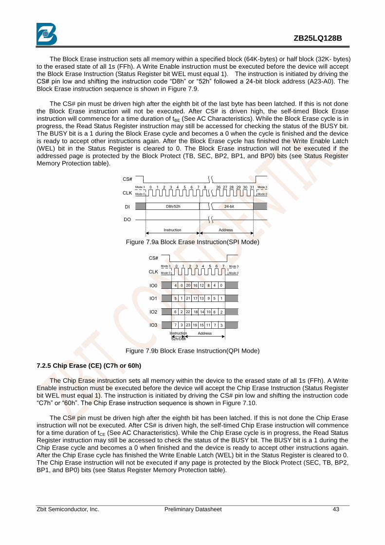
Zbit Semiconductor, Inc. Preliminary Datasheet 43
ZB25LQ128B
The Block Erase instruction sets all memory within a specified block (64K-bytes) or half block (32K- bytes)
to the erased state of all 1s (FFh). A Write Enable instruction must be executed before the device will accept the Block Erase Instruction (Status Register bit WEL must equal 1). The instruction is initiated by driving the CS# pin low and shifting the instruction code ―D8h‖ or ―52h‖ followed a 24-bit block address (A23-A0). The Block Erase instruction sequence is shown in Figure 7.9.
The CS# pin must be driven high after the eighth bit of the last byte has been latched. If this is not done the Block Erase instruction will not be executed. After CS# is driven high, the self-timed Block Erase instruction will commence for a time duration of tBE (See AC Characteristics). While the Block Erase cycle is in progress, the Read Status Register instruction may still be accessed for checking the status of the BUSY bit. The BUSY bit is a 1 during the Block Erase cycle and becomes a 0 when the cycle is finished and the device is ready to accept other instructions again. After the Block Erase cycle has finished the Write Enable Latch (WEL) bit in the Status Register is cleared to 0. The Block Erase instruction will not be executed if the addressed page is protected by the Block Protect (TB, SEC, BP2, BP1, and BP0) bits (see Status Register Memory Protection table).
DI
DO
0
CLK
CS#
1 2 3 4 5 6 7 8 27 28 29 30 31
D8h/52h
Instruction Address
24-bit
26
Mode 0
Mode 3
Mode 0
Mode 3
Figure 7.9a Block Erase Instruction(SPI Mode)
IO0
IO1
0
CLK
CS#
1 3 4 5 6 7
52h/D8h
Instruction Address
2
IO2
IO3
5 1
6 2
7 3
4 0
21
22
23
20
17
18
19
16
13
14
15
12
9
10
11
8 4 0
5 1
6 2
7 3
Mode 0
Mode 3
Mode 0
Mode 3
Figure 7.9b Block Erase Instruction(QPI Mode)
7.2.5 Chip Erase (CE) (C7h or 60h)
The Chip Erase instruction sets all memory within the device to the erased state of all 1s (FFh). A Write
Enable instruction must be executed before the device will accept the Chip Erase Instruction (Status Register bit WEL must equal 1). The instruction is initiated by driving the CS# pin low and shifting the instruction code ―C7h‖ or ―60h‖. The Chip Erase instruction sequence is shown in Figure 7.10.
The CS# pin must be driven high after the eighth bit has been latched. If this is not done the Chip Erase instruction will not be executed. After CS# is driven high, the self-timed Chip Erase instruction will commence for a time duration of tCE (See AC Characteristics). While the Chip Erase cycle is in progress, the Read Status Register instruction may still be accessed to check the status of the BUSY bit. The BUSY bit is a 1 during the Chip Erase cycle and becomes a 0 when finished and the device is ready to accept other instructions again. After the Chip Erase cycle has finished the Write Enable Latch (WEL) bit in the Status Register is cleared to 0. The Chip Erase instruction will not be executed if any page is protected by the Block Protect (SEC, TB, BP2, BP1, and BP0) bits (see Status Register Memory Protection table).

Zbit Semiconductor, Inc. Preliminary Datasheet 44
ZB25LQ128B
DI
DO
0
CLK
CS#
1 2 3 4 5 6 7
C7h/60h
Instruction
Mode 0
Mode 3
Mode 0
Mode 3
IO0
IO1
0
CLK
CS#
1
4 0
5 1
6 2
7 3
IO2
IO3
Instruction
C7h/60h
Mode 0
Mode 3
Mode 0
Mode 3
Figure 7.10 Chip Erase Instruction(SPI or QPI Mode)
7.2.6 Erase / Program Suspend (75h)
The Erase / Program Suspend command allows the system to interrupt a Sector or Block Erase operation, then read from or program data to any other sector. The Erase / Program Suspend command also allows the system to interrupt a Page Program operation and then read from any other page or erase any other sector or block. The Erase / Program Suspend command sequence is shown in Figure 7.11.
The Write Status Registers command (01h,31h,11h), and Erase commands (20h, 52h, D8h, C7h, 60h,
44h) are not allowed during Erase Suspend. Erase Suspend is valid only during the Sector or Block erase operation. If written during the Chip Erase operation, the Erase Suspend command is ignored. The Write Status Registers command (01h,31h,11h), and Program commands (02h, 32h, 42h) are not allowed during Program Suspend. Program Suspend is valid during the Page Program or Quad Page Program operation.
The Erase / Program Suspend command 75h will be accepted by the device only if the SUS bit in the
Status Register equals to 0 and the BUSY bit equals to 1 while a Sector or Block Erase or a Page Program operation is on-going. If the SUS bit equals to 1 or the BUSY bit equals to 0, the Suspend command will be ignored by the device. Program or Erase command for the sector that is being suspended will be ignored.
A maximum of time of tSUS (Section 8.5, AC Electrical Characteristics) is required to suspend the erase or program operation. The BUSY bit in the Status Register will be cleared from 1 to 0 within tSUS and the SUS bit in the Status Register will be set from 0 to 1 immediately after Erase/Program Suspend. For a previously resumed Erase/Program operation, it is also required that the Suspend command 75h is not issued earlier than a minimum of time of tSUS following the preceding Resume command 7Ah.
Unexpected power off during the Erase / Program suspend state will reset the device and release the suspend state. SUS bit in the Status Register will also reset to 0. The data within the page, sector or block that was being suspended may become corrupted. It is recommended for the user to implement system design techniques to prevent accidental power interruption, provide non-volatile tracking of in process program or erase commands, and preserve data integrity by evaluating the non-volatile program or erase tracking information during each system power up in order to identify and repair (re-erase and re-program) any improperly terminated program or erase operations.
DI
DO
CLK
CS#
75H
Suspend Instruction Read Status Instruction
tsus
Instr.During Suspend
7 6 5 5 4 3 2 1 0
7 6 5 5 4 3 2 1 0
7 6 5 5 4 3 2 1 0
Status
Repeat Status Read Until Suspend
Mode 0
Mode 3
Mode 0
Mode 3
Figure 7.11a Erase / Program Suspend Instruction(SPI Mode)
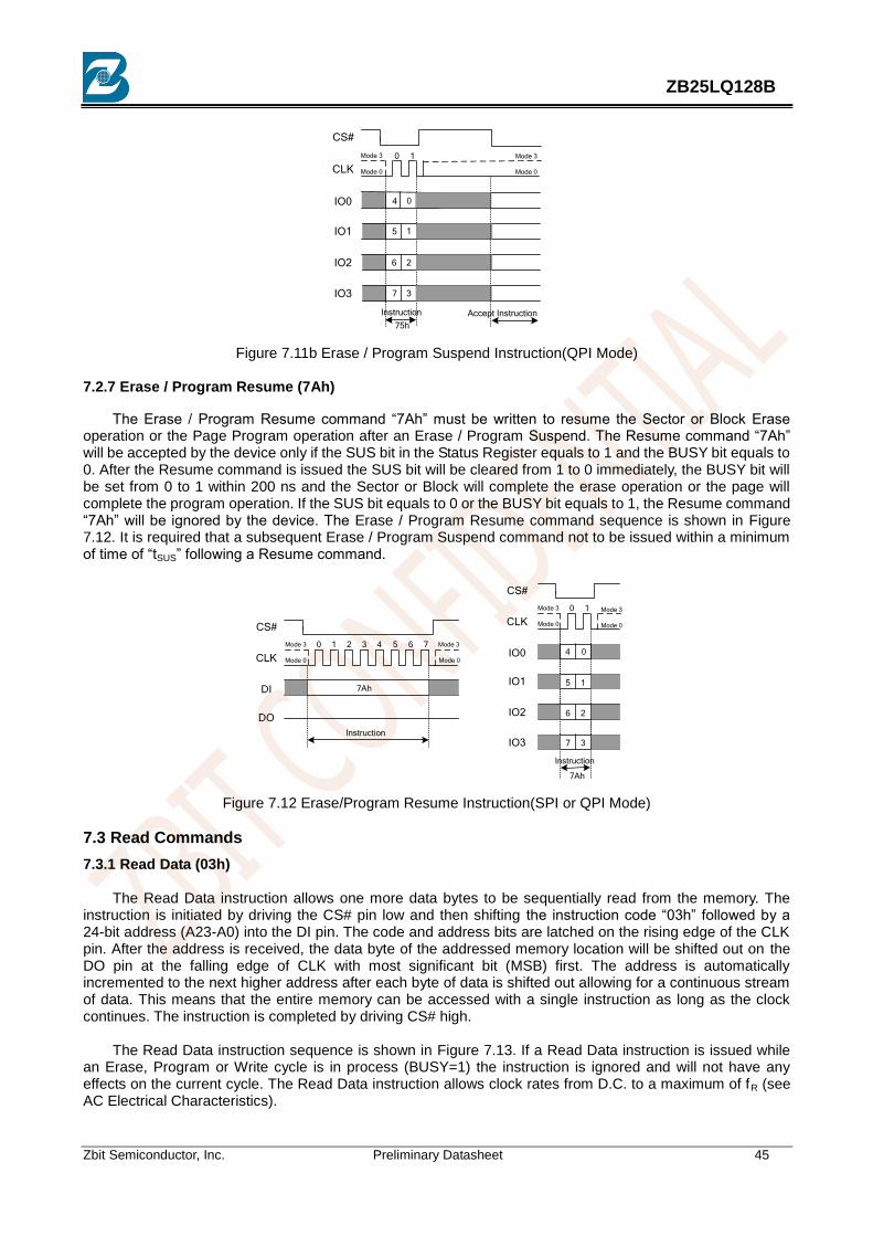
Zbit Semiconductor, Inc. Preliminary Datasheet 45
ZB25LQ128B
IO0
IO1
0
CLK
CS#
1
75h
Instruction
IO2
IO3
5 1
6 2
7 3
4 0
Mode 0
Mode 3
Mode 0
Mode 3
Accept Instruction
Figure 7.11b Erase / Program Suspend Instruction(QPI Mode)
7.2.7 Erase / Program Resume (7Ah)
The Erase / Program Resume command ―7Ah‖ must be written to resume the Sector or Block Erase operation or the Page Program operation after an Erase / Program Suspend. The Resume command ―7Ah‖ will be accepted by the device only if the SUS bit in the Status Register equals to 1 and the BUSY bit equals to 0. After the Resume command is issued the SUS bit will be cleared from 1 to 0 immediately, the BUSY bit will be set from 0 to 1 within 200 ns and the Sector or Block will complete the erase operation or the page will complete the program operation. If the SUS bit equals to 0 or the BUSY bit equals to 1, the Resume command ―7Ah‖ will be ignored by the device. The Erase / Program Resume command sequence is shown in Figure 7.12. It is required that a subsequent Erase / Program Suspend command not to be issued within a minimum of time of ―tSUS‖ following a Resume command.
DI
DO
0
CLK
CS#
1 2 3 4 5 6 7
7Ah
Instruction
Mode 0
Mode 3
Mode 0
Mode 3
IO0
IO1
0
CLK
CS#
1
4 0
5 1
6 2
7 3
IO2
IO3
Instruction
7Ah
Mode 0
Mode 3
Mode 0
Mode 3
Figure 7.12 Erase/Program Resume Instruction(SPI or QPI Mode)
7.3 Read Commands
7.3.1 Read Data (03h) The Read Data instruction allows one more data bytes to be sequentially read from the memory. The
instruction is initiated by driving the CS# pin low and then shifting the instruction code ―03h‖ followed by a 24-bit address (A23-A0) into the DI pin. The code and address bits are latched on the rising edge of the CLK pin. After the address is received, the data byte of the addressed memory location will be shifted out on the DO pin at the falling edge of CLK with most significant bit (MSB) first. The address is automatically incremented to the next higher address after each byte of data is shifted out allowing for a continuous stream of data. This means that the entire memory can be accessed with a single instruction as long as the clock continues. The instruction is completed by driving CS# high.
The Read Data instruction sequence is shown in Figure 7.13. If a Read Data instruction is issued while an Erase, Program or Write cycle is in process (BUSY=1) the instruction is ignored and will not have any effects on the current cycle. The Read Data instruction allows clock rates from D.C. to a maximum of fR (see AC Electrical Characteristics).

Zbit Semiconductor, Inc. Preliminary Datasheet 46
ZB25LQ128B
DI
DO
0
CLK
CS#
1 2 3 4 5 6 7 8 27 28 29 30 31
03h
Instruction Address
24-bit
32 42 43 44 45 46 4739 40 4136 3833 34 35 3726
Output Data 1 Output Data 2
8-bit 8-bit
Mode 0
Mode 3
Mode 0
Mode 3
Figure 7.13 Read Data Instruction
7.3.2 Fast Read (0Bh)
The Fast Read instruction is similar to the Read Data instruction except that it can operate at the highest
possible frequency of FR (see AC Electrical Characteristics). This is accomplished by adding eight ―dummy‖ clocks after the 24-bit address as shown in Figure 7.14. The dummy clocks allow the devices internal circuits additional time for setting up the initial address. During the dummy clocks the data value on the DI pin is a ―don‘t care‖.
DIO
DO
0
CLK
CS#
1 2 3 4 5 6 7 8 27 28 29 30 31
0Bh
Instruction Address
24-bit
32 42 43 44 45 46 4739 40 4136 3833 34 35 3726
Dummy Cycles* Output Data 1
8-bit
Mode 0
Mode 3
Mode 0
Mode 3
Figure 7.14a Fast Read Instruction (SPI Mode)
Fast Read (0Bh) in QPI Mode
The Fast Read instruction is also supported in QPI mode. When QPI mode is enabled, the number of dummy clocks is configured by the ―Set Read Parameters (C0h)‖ instruction to accommodate a wide range of applications with different needs for either maximum Fast Read frequency or minimum data access latency. Depending on the Read Parameter Bits P[5:4] setting, the number of dummy clocks can be configured as either 4, 6, 8 or 8. The default number of dummy clocks upon power up or after a Reset instruction is 4.
0IO0
IO1
CLK
CS#
Instruction Address D1 D2
4 0 4 0 4 0 4 0
5 1 5 1 5 1 5 1
20
21 1
04
15
Dummy*
0Bh
IO2
IO3
6 2 6 2 6 2 6 2
7 3 7 3 7 3 7 3
22
23
2
3
26
37
D3 D4
4 0
5 1
6 2
7 3
Mode 0
Mode 3
4
5
6
7
* “Set Read Parameters” instruction (C0h) can
set number of dummy clocks Figure 7.14b Fast Read Instruction (QPI Mode)
7.3.3 Fast Read Dual Output (3Bh)
The Fast Read Dual Output (3Bh) instruction is similar to the standard Fast Read (0Bh) instruction except
that data is output on two pins, DO and DI, instead of just DO. This allows data to be transferred from the ZB25LQ128B at twice the rate of standard SPI devices. The Fast Read Dual Output instruction is ideal for quickly downloading code from Flash to RAM upon power-up or for applications that cache code-segments to RAM for execution.
Similar to the Fast Read instruction, the Fast Read Dual Output instruction can operate at the highest possible frequency of FR (see AC Electrical Characteristics). This is accomplished by adding eight ―dummy‖ clocks after the 24-bit address as shown in Figure 7.15. The dummy clocks allow the device's internal circuits

Zbit Semiconductor, Inc. Preliminary Datasheet 47
ZB25LQ128B
additional time for setting up the initial address. The input data during the dummy clocks is ―don‘t care‖. However, the DI pin should be high-impedance prior to the falling edge of the first data out clock.
DIO
DO
0
CLK
CS#
1 2 3 4 5 6 7 8 27 28 29 30 31
3Bh
Instruction Address
24-bit
32 42 43 44 45 46 4739 40 4136 3833 34 35 3726
Dummy Cycles* Data 1 Data 2
6 4 2 0 6 4 2 0
7 5 3 1 7 5 3 1
Mode 0
Mode 3
Mode 0
Mode 3
Figure 7.15 Fast Read Dual Output Instruction Sequence Diagram
7.3.4 Fast Read Quad Output (6Bh)
The Fast Read Quad Output (6Bh) instruction is similar to the Fast Dual Output (3Bh) instruction except that data is output on four pins, IO0, IO1, IO2 and IO3. A Quad enable of status Register-2 must be executed before the device will accept the Fast Read Quad Output Instruction (Status Register bit QE must equal 1). The Fast Read Quad Output Instruction allows data to be transferred from ZB25LQ128B at four times the rate of standard SPI devices.
The Fast Read Quad Output instruction can operate at the highest possible frequency of FR (see AC Electrical Characteristics). This is accomplished by adding "dummy" clocks after the 24-bit address as shown in Figure 7.16. The input data during the dummy clocks is "don't care". However, the IO pins should be high-impedance prior to the falling edge of the first data out clock.
IO0
IO1
0
CLK
CS#
1 2 3 4 5 6 7 8 27 28 29 30 31
6Bh
Instruction Address
24-bit
32 42 43 44 45 46 4739 40 4136 3833 34 35 3726
Dummy Cycles* D1 D2
4 0 4 0 4 0 4 0
5 1 5 1 5 1 5 1
IO2 6 2 6 2 6 2 6 2
IO3 7 3 7 3 7 3 7 3
D3 D4
Mode 0
Mode 3
Mode 0
Mode 3
Figure 7.16 Fast Read Quad Output Instruction
7.3.5 Fast Read Dual I/O (BBh)
The Fast Read Dual I/O (BBh) instruction allows for improved random access while maintaining two IO pins, IO0 and IO1. It is similar to the Fast Read Dual Output (3Bh) instruction but with the capability to input the Address bits (A23-0) two bits per dock. This reduced instruction overhead may allow for code execution (XIP) directly from the Dual SPI in some applications. Fast Read Dual I/O with "Continuous Read Mode"
The Fast Read Dual I/O instruction can further reduce instruction overhead through setting the "Continuous Read Mode" bits (M7-0) after the input Address bits (A23-0), as shown in Figure 7.17. The upper nibble of the (M7-4) controls the length of the next Fast Read Dual I/O instruction through the inclusion or exclusion of the first byte instruction code. The lower nibble bits of the (M3-0) are don't care ("X"). However, the IO pins should be high-impedance prior to the falling edge of the first data out clock. It is recommended to input FFFFh on IO0 for the next instruction (16 clocks), to ensure M4 = 1 and return the device to normal operation.
IO0
IO1
0
CLK
CS#
1 2 3 4 5 6 7 8 19 20 21 22 23
Instruction Address
24 3128 3025 26 27 2918
Data 1 Data 2
6 4 2 0 6 4 2 0
7 5 3 1 7 5 3 1
22
23
0246
1357
02
13
Mode
BBh
Mode 0
Mode 3
Figure 7.17 Fast Read Dual I/O Instruction (Initial command or previous M5-4≠10)
Note: 1. Least significant 4 bits of Mode are don‘t care and it is optional for the host to drive these bits. The host may turn off drive during these

Zbit Semiconductor, Inc. Preliminary Datasheet 48
ZB25LQ128B
cycles to increase bus turnaround time between Mode bits from host and returning data from the memory
IO0
IO1
CLK
CS#
DataN Address Data 1 Data 2
6 4 2 0 6 4 2 0
7 5 3 1 7 5 3 1
22
23
0246
1357
02
13
Mode
0246
1357
Figure 7.18 Fast Read Dual I/O Instruction (Initial command or previous M5-4=10)
7.3.6 Fast Read Quad I/O (EBh)
The Fast Read Quad I/O (EBh) command is similar to the Fast Read Dual I/O (BBh) command except that address and data bits are input and output through four pins IO0, IO1, IO2 and IO3 and Dummy clock are required prior to the data output. The Quad I/O dramatically reduces instruction overhead allowing faster random access for code execution (XIP) directly from the Quad SPI. The Quad Enable bit (QE) of Status Register-2 must be set to enable the Fast Read Quad I/O Command. Fast Read Quad I/O with “Continuous Read Mode”
The Fast Read Quad I/O command can further reduce instruction overhead through setting the ―Continuous Read Mode‖ bits (M7-0) after the input Address bits (A23-0), as shown in Figure 7.19, Fast Read
Quad I/O Command Sequence (Initial command or previous M5-4≠10). The upper nibble of the (M7-4)
controls the length of the next Fast Read Quad I/O command through the inclusion or exclusion of the first byte instruction code. The lower nibble bits of the (M3-0) are don‘t care (―X‖). However, the IO pins should be high-impedance prior to the falling edge of the first data out clock.
If the ―Continuous Read Mode‖ bits M5-4 = (1,0), then the next Fast Read Quad I/O command (after CS# is raised and then lowered) does not require the EBh instruction code, as shown in Figure 7.20, Fast Read Quad I/O Command Sequence (Previous command set M5-4 = 10). This reduces the command sequence by eight clocks and allows the Read address to be immediately entered after CS# is asserted low. If the ―Continuous Read Mode‖ bits M5-4 do not equal to (1, 0), the next command (after CS# is raised and then lowered) requires the first byte instruction code, thus returning to normal operation. It is recommended to input FFh on IO0 for the next instruction (8 clocks), to ensure M4=1 and return the device to normal operation.
0IO0
IO1
CLK
CS#
Instruction Address D1 D2
4 0 4 0 4 0 4 0
5 1 5 1 5 1 5 1
20
21
4
15
04
15
Mode
EBh
IO2
IO3
6 2 6 2 6 2 6 2
7 3 7 3 7 3 7 3
22
23
26
3
26
37 7
Dummy* D3 D4
Mode 0
Mode 3
Figure 7.19a Fast Read Quad I/O Instruction(Initial command or previous M5-4 ≠10)
0IO0
IO1
CLK
CS#
Address D1 D2
4 0 4 0 4 0 4 0
5 1 5 1 5 1 5 1
20
21
4
15
04
15
Mode
404 0
IO2
IO3
6 2 6 2 6 2 6 2
7 3 7 3 7 3 7 3
22
23
26
3
26
37 7
Dummy* D3 D4
515 1
626 2
737 3
DN-1 DN
Figure 7.20 Fast Read Quad I/O Instruction(Previous command set M5-4 = 10)

Zbit Semiconductor, Inc. Preliminary Datasheet 49
ZB25LQ128B
Fast Read Quad I/O with “8/16/32/64-Byte Wrap Around”
The Fast Read Quad I/O command can also be used to access a specific portion within a page by issuing
a ―Set Burst with Wrap‖ command prior to EBh. The ―Set Burst with Wrap‖ command can either enable or disable the ―Wrap Around‖ feature for the following EBh commands. When ―Wrap Around‖ is enabled, the data being accessed can be limited to 8/16/32/64-byte section of data. The output data starts at the initial address specified in the command, once it reaches the ending boundary of the 8/16/32/64-byte section, the output will wrap around to the beginning boundary automatically until CS# is pulled high to terminate the command.
The Burst with Wrap feature allows applications that use cache to quickly fetch a critical address and then fill the cache afterwards within a fixed length (8/16/32/64-bytes) of data without issuing multiple read commands.
The ―Set Burst with Wrap‖ command allows three ―Wrap Bits‖, W6-4 to be set. The W4 bit is used to enable or disable the ―Wrap Around‖ operation while W6-5 is used to specify the length of the wrap around section within a page. See Section 7.3.9, Set Burst with Wrap (77h).
Fast Read Quad I/O (EBh) in QPI Mode
The Fast Read Quad I/O instruction is also supported in QPI mode, as shown in Figure 7.19b When QPI mode is enabled, the number of dummy clocks is configured by the ―Set Read Parameters (C0h)‖ instruction to accommodate a wide range of applications with different needs for either maximum Fast Read frequency or minimum data access latency. Depending on the Read Parameter Bits P[5:4] setting, the number of dummy clocks can be configured as either 4, 6, 8 or 8. The default number of dummy clocks upon power up or after a Reset instruction is 4. In QPI mode, the ―Continuous Read Mode‖ bits M7-0 are also considered as dummy clocks. In the default setting, the data output will follow the Continuous Read Mode bits immediately.
“Continuous Read Mode‖ feature is also available in QPI mode for Fast Read Quad I/O instruction.
Please refer to the description on previous pages.
“Wrap Around‖ feature is not available in QPI mode for Fast Read Quad I/O instruction. To perform a
read operation with fixed data length wrap around in QPI mode, a dedicated ―Burst Read with Wrap‖ (0Ch) instruction must be used. Please refer to 7.5.13 for details.
0IO0
IO1
CLK
CS#
Instruction Address D1 D2
4 0 4 0 4 0 4 0
5 1 5 1 5 1 5 1
20
21 1
04
15
M7-0*
EBh
IO2
IO3
6 2 6 2 6 2 6 2
7 3 7 3 7 3 7 3
22
23
2
3
26
37
D3 D4
4 0
5 1
6 2
7 3
Mode 0
Mode 3
4
5
6
7
* ―Set Read Parameters‖ instruction (C0h) can
set number of dummy clocks Figure 7.19b Fast Read Quad I/O Instruction(Initial command or previous M5-4 ≠10,QPI Mode)
7.3.7 Word Read Quad I/O (E7h)
The Word Read Quad I/O (E7h) instruction is similar to the Fast Quad I/O (EBh) instruction except that
the lowest Address bit (A0) must equal to 0 and only two Dummy clocks are required prior to the data output. The Quad I/O dramatically reduces instruction overhead allowing faster random access for code execution (XIP) directly from the Quad SPI. The Quad Enable bit (QE) of Status Register-2 must be set to enable the Word Read Quad I/O instruction. Word Read Quad I/O with "Continuous Read Mode"
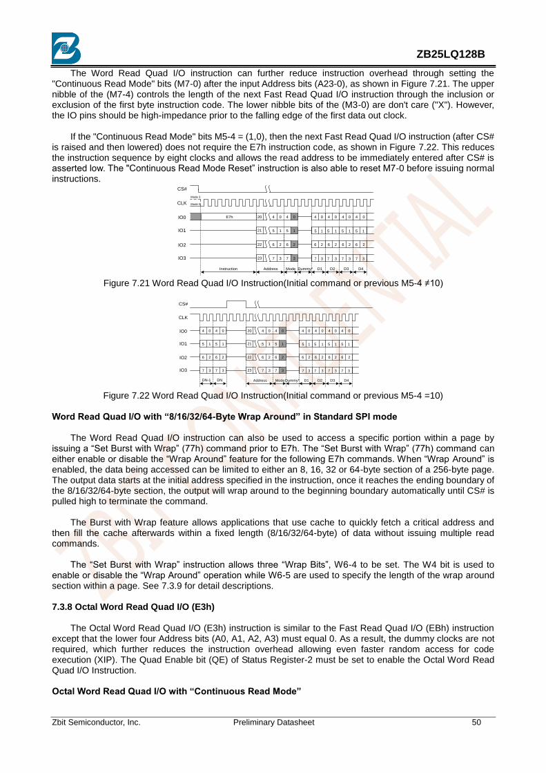
Zbit Semiconductor, Inc. Preliminary Datasheet 50
ZB25LQ128B
The Word Read Quad I/O instruction can further reduce instruction overhead through setting the "Continuous Read Mode" bits (M7-0) after the input Address bits (A23-0), as shown in Figure 7.21. The upper nibble of the (M7-4) controls the length of the next Fast Read Quad I/O instruction through the inclusion or exclusion of the first byte instruction code. The lower nibble bits of the (M3-0) are don't care ("X"). However, the IO pins should be high-impedance prior to the falling edge of the first data out clock.
If the "Continuous Read Mode" bits M5-4 = (1,0), then the next Fast Read Quad I/O instruction (after CS# is raised and then lowered) does not require the E7h instruction code, as shown in Figure 7.22. This reduces the instruction sequence by eight clocks and allows the read address to be immediately entered after CS# is asserted low. The "Continuous Read Mode Reset‖ instruction is also able to reset M7-0 before issuing normal instructions.
0IO0
IO1
CLK
CS#
Instruction Address D1 D2
4 0 4 0 4 0 4 0
5 1 5 1 5 1 5 1
20
21
4
15
04
15
Mode
E7h
IO2
IO3
6 2 6 2 6 2 6 2
7 3 7 3 7 3 7 3
22
23
26
3
26
37 7
Dummy* D3 D4
Mode 0
Mode 3
Figure 7.21 Word Read Quad I/O Instruction(Initial command or previous M5-4 ≠10)
0IO0
IO1
CLK
CS#
Address D1 D2
4 0 4 0 4 0 4 0
5 1 5 1 5 1 5 1
20
21
4
15
04
15
Mode
404 0
IO2
IO3
6 2 6 2 6 2 6 2
7 3 7 3 7 3 7 3
22
23
26
3
26
37 7
Dummy* D3 D4
515 1
626 2
737 3
DN-1 DN
Figure 7.22 Word Read Quad I/O Instruction(Initial command or previous M5-4 =10)
Word Read Quad I/O with “8/16/32/64-Byte Wrap Around” in Standard SPI mode
The Word Read Quad I/O instruction can also be used to access a specific portion within a page by
issuing a ―Set Burst with Wrap‖ (77h) command prior to E7h. The ―Set Burst with Wrap‖ (77h) command can either enable or disable the ―Wrap Around‖ feature for the following E7h commands. When ―Wrap Around‖ is enabled, the data being accessed can be limited to either an 8, 16, 32 or 64-byte section of a 256-byte page. The output data starts at the initial address specified in the instruction, once it reaches the ending boundary of the 8/16/32/64-byte section, the output will wrap around to the beginning boundary automatically until CS# is pulled high to terminate the command.
The Burst with Wrap feature allows applications that use cache to quickly fetch a critical address and then fill the cache afterwards within a fixed length (8/16/32/64-byte) of data without issuing multiple read commands.
The ―Set Burst with Wrap‖ instruction allows three ―Wrap Bits‖, W6-4 to be set. The W4 bit is used to
enable or disable the ―Wrap Around‖ operation while W6-5 are used to specify the length of the wrap around section within a page. See 7.3.9 for detail descriptions.
7.3.8 Octal Word Read Quad I/O (E3h)
The Octal Word Read Quad I/O (E3h) instruction is similar to the Fast Read Quad I/O (EBh) instruction except that the lower four Address bits (A0, A1, A2, A3) must equal 0. As a result, the dummy clocks are not required, which further reduces the instruction overhead allowing even faster random access for code execution (XIP). The Quad Enable bit (QE) of Status Register-2 must be set to enable the Octal Word Read Quad I/O Instruction. Octal Word Read Quad I/O with “Continuous Read Mode”

Zbit Semiconductor, Inc. Preliminary Datasheet 51
ZB25LQ128B
The Octal Word Read Quad I/O instruction can further reduce instruction overhead through setting the ―Continuous Read Mode‖ bits (M7-0) after the input Address bits (A23-0), as shown in Figure 7.23. The upper nibble of the (M7-4) controls the length of the next Octal Word Read Quad I/O instruction through the inclusion or exclusion of the first byte instruction code. The lower nibble bits of the (M3-0) are don‘t care (―x‖). However, the IO pins should be high-impedance prior to the falling edge of the first data out clock. If the ―Continuous Read Mode‖ bits M5-4 = (1,0), then the next Fast Read Quad I/O instruction (after CS# is raised and then lowered) does not require the E3h instruction code, as shown in Figure 7.24. This reduces the instruction sequence by eight clocks and allows the Read address to be immediately entered after CS# is asserted low. If the ―Continuous Read Mode‖ bits M5-4 do not equal to (1,0), the next instruction (after CS# is raised and then lowered) requires the first byte instruction code, thus returning to normal operation. It is recommended to input FFh on IO0 for the next instruction (8 clocks), to ensure M4= 1 and return the device to normal operation.
0IO0
IO1
CLK
CS#
Instruction Address D1 D2
4 0 4 0 4 0 4 0
5 1 5 1 5 1 5 1
20
21
4
15
04
15
Mode
E3h
IO2
IO3
6 2 6 2 6 2 6 2
7 3 7 3 7 3 7 3
22
23
26
3
26
37 7
D3 D4
Mode 0
Mode 3
Figure 7.23 Octal Word Read Quad I/O Instruction(Initial command or previous M5-4 ≠10)
0IO0
IO1
CLK
CS#
Address D1 D2
4 0 4 0 4 0 4 0
5 1 5 1 5 1 5 1
20
21
4
15
04
15
Mode
404 0
IO2
IO3
6 2 6 2 6 2 6 2
7 3 7 3 7 3 7 3
22
23
26
3
26
37 7
D3 D4
515 1
626 2
737 3
DN-1 DN
Figure 7.24 Octal Word Read Quad I/O Instruction(Initial command or previous M5-4 =10)
7.3.9 Set Burst with Wrap (77h)
The Set Burst with Wrap (77h) command is used in conjunction with ―Fast Read Quad I/O‖ commands to access a fixed length and alignment of 8/16/32/64-bytes of data. Certain applications can benefit from this feature and improve the overall system code execution performance. This command loads the W4,W5,W6 bits. Similar to a Quad I/O command, the Set Burst with Wrap command is initiated by driving the CS# pin low and then shifting the instruction code ―77h‖ followed by 24-dummy bits and 8 ―Wrap Bits‖, W7-0. The command sequence is shown in Figure 7.25, Set Burst with Wrap Command Sequence. Wrap bit W7 and the lower nibble W3-0 are not used.
W6, W5 W4=0 W4=1(DEFAULT)
Wrap Around Wrap Length Wrap Around Wrap Length
0,0 Yes 8-byte No N/A
0,1 Yes 16-byte No N/A
1,0 Yes 32-byte No N/A
1,1 Yes 64-byte No N/A
Once W6-4 is set by a Set Burst with Wrap command, all the following ―Fast Read Quad I/O‖ commands
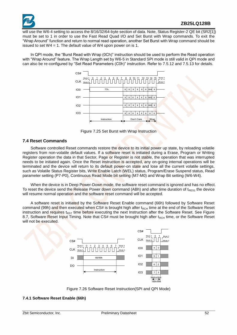
Zbit Semiconductor, Inc. Preliminary Datasheet 52
ZB25LQ128B
will use the W6-4 setting to access the 8/16/32/64-byte section of data. Note, Status Register-2 QE bit (SR2[1]) must be set to 1 in order to use the Fast Read Quad I/O and Set Burst with Wrap commands. To exit the ―Wrap Around‖ function and return to normal read operation, another Set Burst with Wrap command should be issued to set W4 = 1. The default value of W4 upon power on is 1.
In QPI mode, the ―Burst Read with Wrap (0Ch)‖ instruction should be used to perform the Read operation with ―Wrap Around‖ feature. The Wrap Length set by W6-5 in Standard SPI mode is still valid in QPI mode and can also be re-configured by ―Set Read Parameters (C0h)‖ instruction. Refer to 7.5.12 and 7.5.13 for details.
IO0
IO1
CLK
CS#
Instruction
X X X X X X W4 X
X X X X X X W5 X
77h
IO2
IO3
X X X X X X W6 X
X X X X X X X X
Don’t Care Wrap
0 1 2 3 4 5 6 7 8 9 10 11 12 13 14 15
Mode 0
Mode 3
Mode 0
Mode 3
Figure 7.25 Set Burst with Wrap Instruction
7.4 Reset Commands
Software controlled Reset commands restore the device to its initial power up state, by reloading volatile registers from non-volatile default values. If a software reset is initiated during a Erase, Program or Writing Register operation the data in that Sector, Page or Register is not stable, the operation that was interrupted needs to be initiated again. Once the Reset instruction is accepted, any on-going internal operations will be terminated and the device will return to its default power-on state and lose all the current volatile settings, such as Volatile Status Register bits, Write Enable Latch (WEL) status, Program/Erase Suspend status, Read parameter setting (P7-P0), Continuous Read Mode bit setting (M7-M0) and Wrap Bit setting (W6-W4).
When the device is in Deep Power-Down mode, the software reset command is ignored and has no effect. To reset the device send the Release Power down command (ABh) and after time duration of tRES1 the device will resume normal operation and the software reset command will be accepted.
A software reset is initiated by the Software Reset Enable command (66h) followed by Software Reset command (99h) and then executed when CS# is brought high after tRCH time at the end of the Software Reset instruction and requires tRST time before executing the next Instruction after the Software Reset. See Figure 8.7, Software Reset Input Timing. Note that CS# must be brought high after tRCH time, or the Software Reset will not be executed.
DI
DO
0
CLK
CS#
1 2 3 4 5 6 7
66/99h
Instruction
Mode 0
Mode 3
Mode 0
Mode 3
IO0
IO1
0
CLK
CS#
1
4 0
5 1
6 2
7 3
IO2
IO3
Instruction
66h/99h
Mode 0
Mode 3
Mode 0
Mode 3
Figure 7.26 Software Reset Instruction(SPI and QPI Mode)
7.4.1 Software Reset Enable (66h)
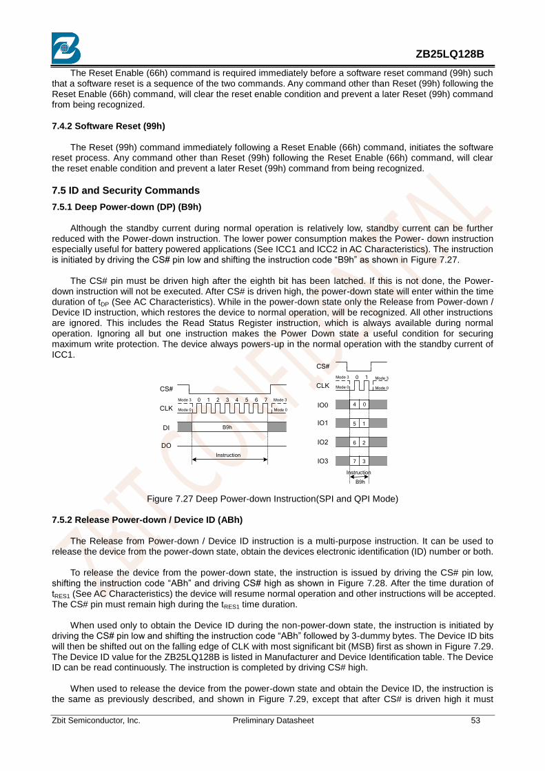
Zbit Semiconductor, Inc. Preliminary Datasheet 53
ZB25LQ128B
The Reset Enable (66h) command is required immediately before a software reset command (99h) such that a software reset is a sequence of the two commands. Any command other than Reset (99h) following the Reset Enable (66h) command, will clear the reset enable condition and prevent a later Reset (99h) command from being recognized.
7.4.2 Software Reset (99h)
The Reset (99h) command immediately following a Reset Enable (66h) command, initiates the software reset process. Any command other than Reset (99h) following the Reset Enable (66h) command, will clear the reset enable condition and prevent a later Reset (99h) command from being recognized.
7.5 ID and Security Commands
7.5.1 Deep Power-down (DP) (B9h)
Although the standby current during normal operation is relatively low, standby current can be further reduced with the Power-down instruction. The lower power consumption makes the Power- down instruction especially useful for battery powered applications (See ICC1 and ICC2 in AC Characteristics). The instruction is initiated by driving the CS# pin low and shifting the instruction code ―B9h‖ as shown in Figure 7.27.
The CS# pin must be driven high after the eighth bit has been latched. If this is not done, the Power- down instruction will not be executed. After CS# is driven high, the power-down state will enter within the time duration of tDP (See AC Characteristics). While in the power-down state only the Release from Power-down / Device ID instruction, which restores the device to normal operation, will be recognized. All other instructions are ignored. This includes the Read Status Register instruction, which is always available during normal operation. Ignoring all but one instruction makes the Power Down state a useful condition for securing maximum write protection. The device always powers-up in the normal operation with the standby current of ICC1.
DI
DO
0
CLK
CS#
1 2 3 4 5 6 7
B9h
Instruction
Mode 0
Mode 3
Mode 0
Mode 3
IO0
IO1
0
CLK
CS#
1
4 0
5 1
6 2
7 3
IO2
IO3
Instruction
B9h
Mode 0
Mode 3
Mode 0
Mode 3
Figure 7.27 Deep Power-down Instruction(SPI and QPI Mode)
7.5.2 Release Power-down / Device ID (ABh)
The Release from Power-down / Device ID instruction is a multi-purpose instruction. It can be used to release the device from the power-down state, obtain the devices electronic identification (ID) number or both.
To release the device from the power-down state, the instruction is issued by driving the CS# pin low, shifting the instruction code ―ABh‖ and driving CS# high as shown in Figure 7.28. After the time duration of tRES1 (See AC Characteristics) the device will resume normal operation and other instructions will be accepted. The CS# pin must remain high during the tRES1 time duration.
When used only to obtain the Device ID during the non-power-down state, the instruction is initiated by driving the CS# pin low and shifting the instruction code ―ABh‖ followed by 3-dummy bytes. The Device ID bits will then be shifted out on the falling edge of CLK with most significant bit (MSB) first as shown in Figure 7.29. The Device ID value for the ZB25LQ128B is listed in Manufacturer and Device Identification table. The Device ID can be read continuously. The instruction is completed by driving CS# high.
When used to release the device from the power-down state and obtain the Device ID, the instruction is the same as previously described, and shown in Figure 7.29, except that after CS# is driven high it must

Zbit Semiconductor, Inc. Preliminary Datasheet 54
ZB25LQ128B
remain high for a time duration of tRES2 (See AC Characteristics). After this time duration the device will resume normal operation and other instructions will be accepted. If the Release from Power-down / Device ID instruction is issued within Erase, Program or Write cycle (when BUSY equals 1), the instruction is ignored and will not have any effects on the current cycle.
DI
DO
0
CLK
CS#
1 2 3 4 5 6 7
ABh
Instruction
Mode 0
Mode 3
Mode 0
Mode 3
IO0
IO1
0
CLK
CS#
1
4 0
5 1
6 2
7 3
IO2
IO3
Instruction
ABh
Mode 0
Mode 3
Mode 0
Mode 3
Figure 7.28 Release Power-down Instruction(SPI and QPI Mode)
DI
DO
0
CLK
CS#
1 2 3 4 5 6 7 8 27 28 29 30 31
ABh
Instruction Dummy
24-bit
32 3936 3833 34 35 3726
Device ID
7 6 5 4 3 2 1 0
Mode 0
Mode 3
Mode 0
Mode 3
Figure 7.29a Release Power-down / Device ID(SPI Mode)
IO0
IO1
0
CLK
CS#
1 3 4 5 6 7
ABh
Instruction Dummy
8 9 10 112
IO2
IO3
4 0 4 0
5 1 5 1
6 2 6 2
7 3 7 3
DEID DEID
5 1
6 2
7 3
4 0
21
22
23
20
17
18
19
16
13
14
15
12
9
10
11
8 4 0
5 1
6 2
7 3
Mode 0
Mode 3
Mode 0
Mode 3
Figure 7.29b Release Power-down / Device ID(QPI Mode)
7.5.3 Read Manufacturer / Device ID (90h)
The Read Manufacturer/Device ID instruction is an alternative to the Release from Power-down/Device ID instruction that provides both the JEDEC assigned manufacturer ID and the specific device ID.
The Read Manufacturer/Device ID instruction is very similar to the Release from Power-down / Device ID instruction. The instruction is initiated by driving the CS# pin low and shifting the instruction code ―90h‖ followed by a 24-bit address (A23-A0) of 000000h. After which, the Manufacturer ID and the Device ID are shifted out on the falling edge of CLK with most significant bit (MSB) first as shown in Figure 7.30. If the 24-bit address is initially set to 000001h the Device ID will be read first and then followed by the Manufacturer ID. The Manufacturer and Device IDs can be read continuously, alternating from one to the other. The command is completed by driving CS# high.

Zbit Semiconductor, Inc. Preliminary Datasheet 55
ZB25LQ128B
DI
DO
0
CLK
CS#
1 2 3 4 5 6 7 8 27 28 29 30 31
90h
Instruction Address
24-bit
32 42 43 44 45 46 4739 40 4136 3833 34 35 3726
Manufacturer ID Device ID
7 6 5 4 3 2 1 07 6 5 4 3 2 1 0
Mode 0
Mode 3
Mode 0
Mode 3
Figure 7.30a Read Manufacturer/Device ID(SPI Mode)
IO0
IO1
0
CLK
CS#
1 3 4 5 6 7
90h
Instruction Address
8 9 10 112
IO2
IO3
4 0 4 0
5 1 5 1
6 2 6 2
7 3 7 3
MFID DEID
5 1
6 2
7 3
4 0
21
22
23
20
17
18
19
16
13
14
15
12
9
10
11
8 4 0
5 1
6 2
7 3
Mode 0
Mode 3
Mode 0
Mode 3
Figure 7.30b Read Manufacturer/Device ID(QPI Mode)
7.5.4 Read Identification (RDID) (9Fh/AFh)
For compatibility reasons, the ZB25LQ128B provides several instructions to electronically determine the
identity of the device. The Read JEDEC ID instruction is compatible with the JEDEC standard for SPI compatible serial memories that was adopted in 2003.
The instruction is initiated by driving the CS# pin low and shifting the instruction code ―9Fh‖ for SPI, ―9Fh/AFh‖ for QPI. The JEDEC assigned Manufacturer ID byte and two Device ID bytes, Memory Type (ID15-ID8) and Capacity (ID7-ID0) are then shifted out on the falling edge of CLK with most significant bit (MSB) first as shown in Figure 7.31. For memory type and capacity values, refer to Manufacturer and Device Identification table.
DIO
DO
CLK
CS#
9Fh
Instruction Manufacturer ID Memory Type ID
7 6 5 4 3 2 1 07 6 5 4 3 2 1 0 7 6 5 4 3 2 1 0
0 1 2 3 4 5 6 7 8 9 10 11 12 13 14 15 20 21 22 2316 17 18 19 24 25 26 27 28 29 30 31
Capacity ID
Mode 0
Mode 3
Mode 0
Mode 3
Figure 7.31a Read JEDEC ID(SPI Mode)
0 1 3 4 5 6 7
9Fh/AFh
Instruction
8 9 10 112
4 0 4 0
5 1 5 1
6 2 6 2
7 3 7 3
MFID MTID
5 1
6 2
7 3
4 0
5
6
7
4
1
2
3
0
5
6
7
4
1
2
3
0 4 0
5 1
6 2
7 3
Mode 0
Mode 3
Mode 0
Mode 3
4 0
5 1
6 2
7 3
12 13
CAIDCAID MFID MTID
Figure 7.31b Read JEDEC ID(QPI Mode)
7.5.5 Read SFDP Register (5Ah)
The Read SFDP command is initiated by driving the CS# pin low and shifting the instruction code ―5Ah‖
followed by a 24-bit address (A23-A0) into the DI pin. Eight ―dummy‖ clocks are also required before the SFDP register contents are shifted out on the falling edge of the 40th CLK with most significant bit (MSB) first as shown in Figure 7.32.
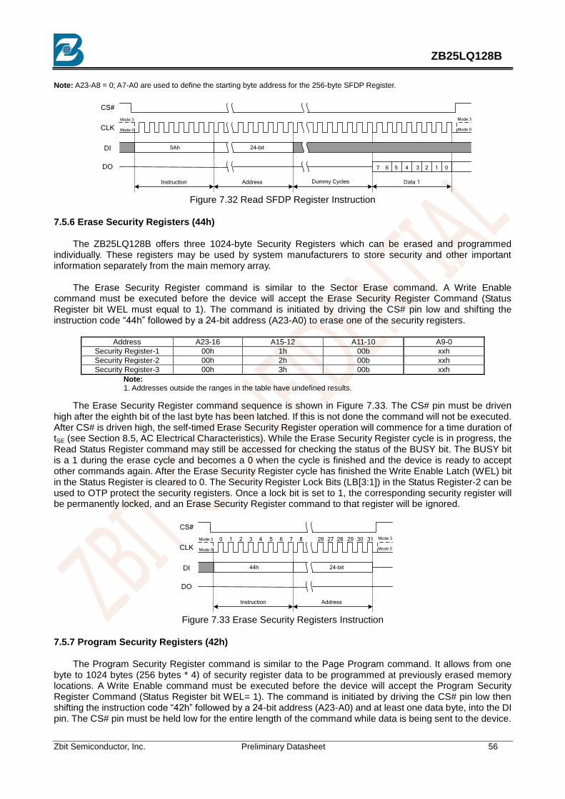
Zbit Semiconductor, Inc. Preliminary Datasheet 56
ZB25LQ128B
Note: A23-A8 = 0; A7-A0 are used to define the starting byte address for the 256-byte SFDP Register.
DI
DO
CLK
CS#
5Ah
Instruction Address
24-bit
Dummy Cycles Data 1
7 6 5 4 3 2 1 0
Mode 0
Mode 3
Mode 0
Mode 3
Figure 7.32 Read SFDP Register Instruction
7.5.6 Erase Security Registers (44h)
The ZB25LQ128B offers three 1024-byte Security Registers which can be erased and programmed individually. These registers may be used by system manufacturers to store security and other important information separately from the main memory array.
The Erase Security Register command is similar to the Sector Erase command. A Write Enable
command must be executed before the device will accept the Erase Security Register Command (Status Register bit WEL must equal to 1). The command is initiated by driving the CS# pin low and shifting the instruction code ―44h‖ followed by a 24-bit address (A23-A0) to erase one of the security registers.
Address A23-16 A15-12 A11-10 A9-0
Security Register-1 00h 1h 00b xxh
Security Register-2 00h 2h 00b xxh
Security Register-3 00h 3h 00b xxh
Note: 1. Addresses outside the ranges in the table have undefined results.
The Erase Security Register command sequence is shown in Figure 7.33. The CS# pin must be driven high after the eighth bit of the last byte has been latched. If this is not done the command will not be executed. After CS# is driven high, the self-timed Erase Security Register operation will commence for a time duration of tSE (see Section 8.5, AC Electrical Characteristics). While the Erase Security Register cycle is in progress, the Read Status Register command may still be accessed for checking the status of the BUSY bit. The BUSY bit is a 1 during the erase cycle and becomes a 0 when the cycle is finished and the device is ready to accept other commands again. After the Erase Security Register cycle has finished the Write Enable Latch (WEL) bit in the Status Register is cleared to 0. The Security Register Lock Bits (LB[3:1]) in the Status Register-2 can be used to OTP protect the security registers. Once a lock bit is set to 1, the corresponding security register will be permanently locked, and an Erase Security Register command to that register will be ignored.
DI
DO
0
CLK
CS#
1 2 3 4 5 6 7 8 27 28 29 30 31
44h
Instruction Address
24-bit
26
Mode 0
Mode 3
Mode 0
Mode 3
Figure 7.33 Erase Security Registers Instruction
7.5.7 Program Security Registers (42h)
The Program Security Register command is similar to the Page Program command. It allows from one byte to 1024 bytes (256 bytes * 4) of security register data to be programmed at previously erased memory locations. A Write Enable command must be executed before the device will accept the Program Security Register Command (Status Register bit WEL= 1). The command is initiated by driving the CS# pin low then shifting the instruction code ―42h‖ followed by a 24-bit address (A23-A0) and at least one data byte, into the DI pin. The CS# pin must be held low for the entire length of the command while data is being sent to the device.
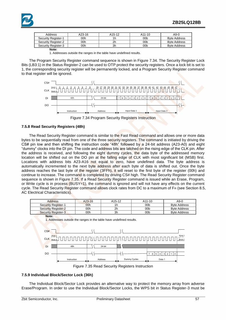
Zbit Semiconductor, Inc. Preliminary Datasheet 57
ZB25LQ128B
Address A23-16 A15-12 A11-10 A9-0
Security Register-1 00h 1h 00b Byte Address
Security Register-2 00h 2h 00b Byte Address
Security Register-3 00h 3h 00b Byte Address
Note: 1. Addresses outside the ranges in the table have undefined results.
The Program Security Register command sequence is shown in Figure 7.34. The Security Register Lock Bits (LB3:1) in the Status Register-2 can be used to OTP protect the security registers. Once a lock bit is set to 1, the corresponding security register will be permanently locked, and a Program Security Register command to that register will be ignored.
DI
DO
0
CLK
CS#
1 2 3 4 5 6 7 8 27 28 29 30 31
42h
Instruction Address
24-bit
32 42 43 44 45 46 4739 40 4136 3833 34 35 3726
Input Data 1 Input Data 2
7 6 5 4 3 2 1 07 6 5 4 3 2 1 0
Mode 0
Mode 3
Figure 7.34 Program Security Registers Instruction
7.5.8 Read Security Registers (48h)
The Read Security Register command is similar to the Fast Read command and allows one or more data
bytes to be sequentially read from one of the three security registers. The command is initiated by driving the CS# pin low and then shifting the instruction code ―48h‖ followed by a 24-bit address (A23-A0) and eight ―dummy‖ clocks into the DI pin. The code and address bits are latched on the rising edge of the CLK pin. After the address is received, and following the eight dummy cycles, the data byte of the addressed memory location will be shifted out on the DO pin at the falling edge of CLK with most significant bit (MSB) first. Locations with address bits A23-A16 not equal to zero, have undefined data. The byte address is automatically incremented to the next byte address after each byte of data is shifted out. Once the byte address reaches the last byte of the register (3FFh), it will reset to the first byte of the register (00h) and continue to increase. The command is completed by driving CS# high. The Read Security Register command sequence is shown in Figure 7.35. If a Read Security Register command is issued while an Erase, Program, or Write cycle is in process (BUSY=1), the command is ignored and will not have any effects on the current cycle. The Read Security Register command allows clock rates from DC to a maximum of FR (see Section 8.5, AC Electrical Characteristics).
Address A23-16 A15-12 A11-10 A9-0
Security Register-1 00h 1h 00b Byte Address
Security Register-2 00h 2h 00b Byte Address
Security Register-3 00h 3h 00b Byte Address
Note: 1. Addresses outside the ranges in the table have undefined results.
DI
DO
CLK
CS#
48h
Instruction Address
24-bit
Dummy Cycles Data 1
7 6 5 4 3 2 1 0
Mode 0
Mode 3
Mode 0
Mode 3
Figure 7.35 Read Security Registers Instruction
7.5.9 Individual Block/Sector Lock (36h)
The Individual Block/Sector Lock provides an alternative way to protect the memory array from adverse
Erase/Program. In order to use the Individual Block/Sector Locks, the WPS bit in Status Register-3 must be

Zbit Semiconductor, Inc. Preliminary Datasheet 58
ZB25LQ128B
set to 1. If WPS=0, the write protection will be determined by the combination of CMP, SEC, TB, BP[2:0] bits in the Status Registers. The Individual Block/Sector Lock bits are volatile bits. The default values after device power up or after a Reset are 1, so the entire memory array is being protected.
To lock a specific block or sector as illustrated in Figure 6.2, an Individual Block/Sector Lock command
must be issued by driving CS# low, shifting the instruction code ―36h‖ into the Data Input (DI) pin on the rising edge of CLK, followed by a 24-bit address and then driving CS# high. A Write Enable instruction must be executed before the device will accept the Individual Block/Sector Lock Instruction (Status Register bit WEL= 1).
DI
DO
0
CLK
CS#
1 2 3 4 5 6 7 8 27 28 29 30 31
36h
Instruction Address
24-bit
26
Mode 0
Mode 3
Mode 0
Mode 3
Figure 7.36a Individual Block/Sector Lock Instruction(SPI Mode)
IO0
IO1
0
CLK
CS#
1 3 4 5 6 7
36h
Instruction Address
2
IO2
IO3
5 1
6 2
7 3
4 0
21
22
23
20
17
18
19
16
13
14
15
12
9
10
11
8 4 0
5 1
6 2
7 3
Mode 0
Mode 3
Mode 0
Mode 3
Figure 7.36b Individual Block/Sector Lock Instruction(QPI Mode)
7.5.10 Individual Block/Sector Unlock (39h)
The Individual Block/Sector Lock provides an alternative way to protect the memory array from adverse
Erase/Program. In order to use the Individual Block/Sector Locks, the WPS bit in Status Register-3 must be set to 1. If WPS=0, the write protection will be determined by the combination of CMP, SEC, TB, BP[2:0] bits in the Status Registers. The Individual Block/Sector Lock bits are volatile bits. The default values after device power up or after a Reset are 1, so the entire memory array is being protected.
To unlock a specific block or sector as illustrated in Figure 6.2, an Individual Block/Sector Unlock
command must be issued by driving CS# low, shifting the instruction code ―39h‖ into the Data Input (DI) pin on the rising edge of CLK, followed by a 24-bit address and then driving CS# high. A Write Enable instruction must be executed before the device will accept the Individual Block/Sector Unlock Instruction(Status Register bit WEL= 1).
DI
DO
0
CLK
CS#
1 2 3 4 5 6 7 8 27 28 29 30 31
39h
Instruction Address
24-bit
26
Mode 0
Mode 3
Mode 0
Mode 3
Figure 7.37a Individual Block/Sector Unlock Instruction(SPI Mode)
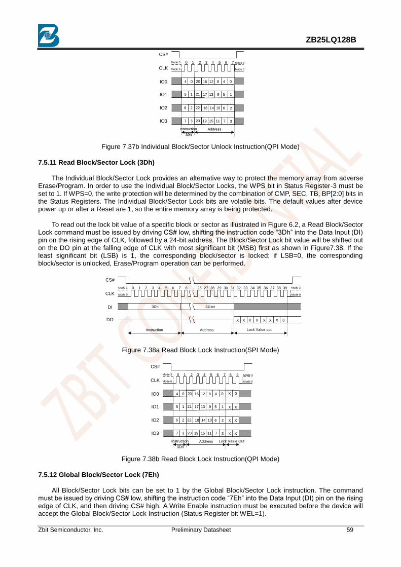
Zbit Semiconductor, Inc. Preliminary Datasheet 59
ZB25LQ128B
IO0
IO1
0
CLK
CS#
1 3 4 5 6 7
39h
Instruction Address
2
IO2
IO3
5 1
6 2
7 3
4 0
21
22
23
20
17
18
19
16
13
14
15
12
9
10
11
8 4 0
5 1
6 2
7 3
Mode 0
Mode 3
Mode 0
Mode 3
Figure 7.37b Individual Block/Sector Unlock Instruction(QPI Mode)
7.5.11 Read Block/Sector Lock (3Dh)
The Individual Block/Sector Lock provides an alternative way to protect the memory array from adverse
Erase/Program. In order to use the Individual Block/Sector Locks, the WPS bit in Status Register-3 must be set to 1. If WPS=0, the write protection will be determined by the combination of CMP, SEC, TB, BP[2:0] bits in the Status Registers. The Individual Block/Sector Lock bits are volatile bits. The default values after device power up or after a Reset are 1, so the entire memory array is being protected.
To read out the lock bit value of a specific block or sector as illustrated in Figure 6.2, a Read Block/Sector
Lock command must be issued by driving CS# low, shifting the instruction code ―3Dh‖ into the Data Input (DI) pin on the rising edge of CLK, followed by a 24-bit address. The Block/Sector Lock bit value will be shifted out on the DO pin at the falling edge of CLK with most significant bit (MSB) first as shown in Figure7.38. If the least significant bit (LSB) is 1, the corresponding block/sector is locked; if LSB=0, the corresponding block/sector is unlocked, Erase/Program operation can be performed.
DI
DO
0
CLK
CS#
1 2 3 4 5 6 7 8 27 28 29 30 31
3Dh
Instruction Address
24-bit
32 3936 3833 34 35 3726
Lock Value out
X X X X X X X 0
Mode 0
Mode 3
Mode 0
Mode 3
Figure 7.38a Read Block Lock Instruction(SPI Mode)
IO0
IO1
0
CLK
CS#
1 3 4 5 6 7
3Dh
Instruction Address
8 92
IO2
IO3
X 0
X X
X X
X X
Lock Value Out
5 1
6 2
7 3
4 0
21
22
23
20
17
18
19
16
13
14
15
12
9
10
11
8 4 0
5 1
6 2
7 3
Mode 0
Mode 3
Mode 0
Mode 3
Figure 7.38b Read Block Lock Instruction(QPI Mode)
7.5.12 Global Block/Sector Lock (7Eh)
All Block/Sector Lock bits can be set to 1 by the Global Block/Sector Lock instruction. The command
must be issued by driving CS# low, shifting the instruction code ―7Eh‖ into the Data Input (DI) pin on the rising edge of CLK, and then driving CS# high. A Write Enable instruction must be executed before the device will accept the Global Block/Sector Lock Instruction (Status Register bit WEL=1).

Zbit Semiconductor, Inc. Preliminary Datasheet 60
ZB25LQ128B
IO0
IO1
0
CLK
CS#
1
4 0
5 1
6 2
7 3
IO2
IO3
Instruction
7Eh
Mode 0
Mode 3
Mode 0
Mode 3
DI
DO
0
CLK
CS#
1 2 3 4 5 6 7
7Eh
Instruction
Mode 0
Mode 3
Mode 0
Mode 3
Figure 7.39 Global Block Lock Instruction(SPI or QPI Mode)
7.5.13 Global Block/Sector Unlock (98h)
All Block/Sector Lock bits can be set to 0 by the Global Block/Sector Unlock instruction. The command
must be issued by driving CS# low, shifting the instruction code ―98h‖ into the Data Input (DI) pin on the rising edge of CLK, and then driving CS# high. A Write Enable instruction must be executed before the device will accept the Global Block/Sector Unlock Instruction (Status Register bit WEL= 1).
IO0
IO1
0
CLK
CS#
1
4 0
5 1
6 2
7 3
IO2
IO3
Instruction
98h
Mode 0
Mode 3
Mode 0
Mode 3
DI
DO
0
CLK
CS#
1 2 3 4 5 6 7
98h
Instruction
Mode 0
Mode 3
Mode 0
Mode 3
Figure 7.40 Global Block Lock Instruction(SPI or QPI Mode)
7.5.14 Read Manufacturer / Device ID Dual I/O (92h)
The Read Manufacturer / Device ID Dual I/O instruction is an alternative to the Read Manufacturer / Device ID instruction that provides both the JEDEC assigned manufacturer ID and the specific device ID at 2x speed.
The Read Manufacturer / Device ID Dual I/O instruction is similar to the Fast Read Dual I/O instruction. The instruction is initiated by driving the CS# pin low and shifting the instruction code ―92h‖ followed by a 24-bit address (A23-A0) of 000000h, but with the capability to input the Address bits two bits per clock. After which, the Manufacturer ID and the Device ID are shifted out 2 bits per clock on the falling edge of CLK with most significant bits (MSB) first as shown in Figure 7.36. The Device ID values for the ZB25LQ128B are listed in Manufacturer and Device Identification table. The Manufacturer and Device IDs can be read continuously, alternating from one to the other. The instruction is completed by driving CS# high.
0IO0
IO1
CLK
CS#
Instruction Address MFID DEID
6 4 2 0 6 4 2 0
7 5 3 1 7 5 3 1
22
23
2
13
46
57
Mode
92h
Mode 0
Mode 3
02
13
4
5
6
7
Figure 7.36 Read Manufacturer/Device ID Dual I/O Instruction
Note:

Zbit Semiconductor, Inc. Preliminary Datasheet 61
ZB25LQ128B
1. The "Continuous Read Mode" bits M7-0 must be set to Fxh to be compatible with Fast Read Dual I/O instruction. 7.5.15 Read Manufacturer / Device ID Quad I/O (94h)
The Read Manufacturer / Device ID Quad I/O instruction is an alternative to Read Manufacturer / Device ID instruction that provides both the JEDEC assigned manufacturer ID and the specific device ID at 4 x speeds.
The Read Manufacturer / Device ID Quad I/O instruction is similar to the Fast Read Quad I/O instruction. The instruction is initiated by driving the CS# pin low and shifting the instruction code "94h" followed by a 24-bit address(A23-A0) of 000000h, 8-bit Continuous Read Mode Bits and then four clock dummy cycles, with the capability to input the Address bits four bits per clock. After that, the Manufacturer ID and the Device ID are shifted out four bits per clock on the falling edge of CLK with most significant bit (MSB) first as shown in Figure 7.37. The Device ID values for ZB25LQ128B are listed in Manufacturer and Device Identification table. The Manufacturer and Device IDs can be read continuously, alternating from one to the other. The instruction is completed by driving CS# high.
0IO0
IO1
CLK
CS#
Instruction Address MFID DEID
4 0 4 0 4 0 4 0
5 1 5 1 5 1 5 1
20
21
4
15
04
15
Mode
IO2
IO3
6 2 6 2 6 2 6 2
7 3 7 3 7 3 7 3
22
23
26
3
26
37 7
Dummy
94h
Dummy MFID DEID
Mode 0
Mode 3
Figure 7.37 Read Manufacturer/Device ID Quad I/O Instruction
Note:
1. The "Continuous Read Mode" bits M7-0 must be set to Fxh to be compatible with Fast Read Quad I/O instruction.
7.5.16 Read Unique ID Number (4Bh)
The Read Unique ID Number instruction accesses a factory-set read-only 128-bit number which is unique to each ZB25LQ128B device. The ID number can be used in conjunction with user software methods to help prevent copying or cloning of a system. The Read Unique ID instruction is initiated by driving the CS# pin low and shifting the instruction code "4Bh" followed by a 24-bit address(A23-A0) of 000000h and one byte dummy
clock. After that, the 128-bit ID is shifted out on the falling edge of CLK as shown in Figure 7.38.
DI
DO
CLK
CS#
4Bh
Instruction Address Dummy Cycles128 bit Unique Serial
Number
3 2 1 0
Mode 0
Mode 3
Mode 0
Mode 3
24-bit 8-bit
126125124127
Figure 7.38 Read unique ID Number Instruction
7.5.17 Set Read Parameters (C0h)
In QPI mode, to accommodate a wide range of applications with different needs for either maximum read
frequency or minimum data access latency, ―Set Read Parameters (C0h)‖ instruction can be used to configure the number of dummy clocks for ―Fast Read (0Bh)‖, ―Fast Read Quad I/O (EBh)‖ & ―Burst Read with Wrap (0Ch)‖ instructions, and to configure the number of bytes of ―Wrap Length‖ for the ―Burst Read with Wrap (0Ch)‖ instruction.

Zbit Semiconductor, Inc. Preliminary Datasheet 62
ZB25LQ128B
In Standard SPI mode, the ―Set Read Parameters (C0h)‖ instruction is not accepted. The ―Wrap Length‖ is set by W6-5 bit in the ―Set Burst with Wrap (77h)‖ instruction. This setting will remain unchanged when the device is switched between Standard SPI mode and QPI mode.
The default ―Wrap Length‖ after a power up or a Reset instruction is 8 bytes, the default number of dummy clocks is 4. The number of dummy clocks is only programmable for ―Fast Read (0Bh)‖, ―Fast Read Quad I/O (EBh)‖ & ―Burst Read with Wrap (0Ch)‖ instructions in the QPI mode. Whenever the device is switched from SPI mode to QPI mode, the number of dummy clocks should be set again, prior to any 0Bh, EBh or 0Ch instructions.
P5-P4 DUMMY CLOCKS
MAXIMUM READ FREQ.
00 4 80MHz
01 6 104MHz
10 8 120MHz
11 8 120MHz
P1-P0 WRAP
LENGTH
00 8-byte
01 16-byte
10 32-byte
11 64-byte
IO0
IO1
0
CLK
CS#
1 2 3
C0h
Instruction Read Parameter
IO2
IO3
5 1
6 2
7 3
4 0 P4 P0
P5 P1
P6 P2
P7 P3
Mode 0
Mode 3
Mode 0
Mode 3
Figure 7.39 Set Read Parameters Instruction (QPI Mode only)
7.5.18 Burst Read with Wrap (0Ch)
The ―Burst Read with Wrap (0Ch)‖ instruction provides an alternative way to perform the read operation with ―Wrap Around‖ in QPI mode. The instruction is similar to the ―Fast Read (0Bh)‖ instruction in QPI mode, except the addressing of the read operation will ―Wrap Around‖ to the beginning boundary of the ―Wrap Length‖ once the ending boundary is reached. The ―Wrap Length‖ and the number of dummy clocks can be configured by the ―Set Read Parameters(C0h)‖ instruction.
0IO0
IO1
CLK
CS#
Instruction Address D1 D2
4 0 4 0 4 0 4 0
5 1 5 1 5 1 5 1
20
21 1
04
15
Dummy*
0Ch
IO2
IO3
6 2 6 2 6 2 6 2
7 3 7 3 7 3 7 3
22
23
2
3
26
37
D3 D4
4 0
5 1
6 2
7 3
Mode 0
Mode 3
4
5
6
7
* “Set Read Parameters” instruction (C0h) can
set number of dummy clocks Figure 7.40 Burst Read with Wrap Instruction (QPI Mode only)
7.5.19 Enter QPI Mode (38h)
The ZB25LQ128B support both Standard/Dual/Quad Serial Peripheral Interface (SPI) and Quad

Zbit Semiconductor, Inc. Preliminary Datasheet 63
ZB25LQ128B
Peripheral Interface (QPI). However, SPI mode and QPI mode cannot be used at the same time. ―Enter QPI (38h)‖ instruction is the only way to switch the device from SPI mode to QPI mode.
Upon power-up, the default state of the device upon is Standard/Dual/Quad SPI mode. This provides full backward compatibility with earlier generations of ZBIT serial flash memories. See Instruction Set Table 7.1-7.4 for all supported SPI commands. In order to switch the device to QPI mode, the Quad Enable (QE) bit in Status Register-2 must be set to 1 first, and an ―Enter QPI (38h)‖ instruction must be issued. If the Quad Enable (QE) bit is 0, the ―Enter QPI (38h)‖ instruction will be ignored and the device will remain in SPI mode. See Instruction Set Table 7.5 for all the commands supported in QPI mode. When the device is switched from SPI mode to QPI mode, the existing Write Enable and Program/Erase Suspend status, and the Wrap Length setting will remain unchanged.
DI
DO
0
CLK
CS#
1 2 3 4 5 6 7
38h
Instruction
Mode 0
Mode 3
Mode 0
Mode 3
Figure 7.41 Enter QPI Instruction (SPI Mode only)
7.5.20 Exit QPI Mode (FFh)
In order to exit the QPI mode and return to the Standard/Dual/Quad SPI mode, an ―Exit QPI (FFh)‖
instruction must be issued. When the device is switched from QPI mode to SPI mode, the existing Write Enable Latch (WEL) and Program/Erase Suspend status, and the Wrap Length setting will remain unchanged.
IO0
IO1
0
CLK
CS#
1
4 0
5 1
6 2
7 3
IO2
IO3
Instruction
FFh
Mode 0
Mode 3
Mode 0
Mode 3
Figure 7.42 Exit QPI Instruction (QPI Mode only)
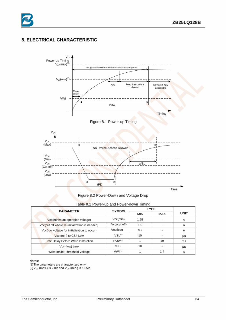
Zbit Semiconductor, Inc. Preliminary Datasheet 64
ZB25LQ128B
8. ELECTRICAL CHARACTERISTIC
VWI
Vcc(min)(2)
Vcc(max)(2)
Power-up Timing
Reset
State
tPUW
tVSL Read Instructions
allowedDevice is fully
accessible
Program Erase and Write Instruction are Igored
Timing
VCC
Figure 8.1 Power-up Timing
VCC
Time
VCC
(Max)
VCC
(Min)
VCC
(Low)
No Device Access Allowed
tPD
tVSLVCC
(Cut off)
Figure 8.2 Power-Down and Voltage Drop
Table 8.1 Power-up and Power-down Timing
PARAMETER SYMBOL TYPE
UNIT MIN MAX
Vcc(minimum operation voltage) Vcc(min) 1.65 - V
Vcc(cut off where re-initialization is needed) Vcc(cut off) 1.0 - V
Vcc(low voltage for initialization to occur) Vcc(low) 0.7 - V
Vcc (min) to CS# Low tVSL(1)
10 - μs
Time Delay Before Write Instruction tPUW(1)
1 10 ms
Vcc (low) time tPD 10 - μs
Write Inhibit Threshold Voltage VWI(1)
1 1.4 V
Notes: (1) The parameters are characterized only. (2) VCC (max.) is 2.0V and VCC (min.) is 1.65V.

Zbit Semiconductor, Inc. Preliminary Datasheet 65
ZB25LQ128B
8.1. Absolute Maximum Ratings
Stresses above the values mentioned as following may cause permanent damage to the device. These
values are for a stress rating only and do not imply that the device should be operated at conditions up to or above these values.
Table 8.2(1)
Absolute Maximum Rating
PARAMETERS(2)
SYMBOL CONDITIONS RANGE UNIT
Supply Voltage VCC -0.6 to +2.5 V
Voltage applied on any pin VIO Relative to Ground -0.6 to VCC+0.4 V
Transient Voltage on any Pin VIOT <20ns Transient Relative to
Ground -2.0 to VCC+2.0 V
Storage Temperature TSTG -65 to +150 ℃
Lead Temperature TLEAD See Note(3)
℃
Electrostatic Discharge Voltage VESD Human Body Model(4)
-2000 to +2000 V
Notes: (1) Specification for ZB25LQ128B is preliminary. See preliminary designation at the end of this document. (2) This device has been designed and tested for the specified operation ranges. Proper operation outside these levels is not guaranteed. Exposure to absolute maximum ratings may affect device reliability. Exposure beyond absolute maximum ratings may cause permanent damage. (3) Compatible to JEDEC Standard J-STD-20C for small body Sn-Pb or Pb-free (Green) assembly and the European directive on restrictions on hazardous substances (RoHS) 2002/95/EU. (4) JEDEC Std. JESD22-A114A (C1=100 pF, R1=1500 ohms, R2=500 ohms).
8.2. Recommended Operating Ranges
Table 8.3 Recommended Operating Ranges
PARAMETER SYMBOL CONDITIONS SPEC
UNIT MIN MAX
Supply Voltage VCC(1)
FR=104MHz,fR=40MHz(2)
1.65 2.0 V
Ambient Temperature, Operating
TA Industrial -40 85 ℃
Notes: (1) Recommended Operating Ranges define those limits between which the functionality of the device is guaranteed. (2) See details Table 8.6 AC Electrical Characteristics.

Zbit Semiconductor, Inc. Preliminary Datasheet 66
ZB25LQ128B
8.3. DC Characteristics
Table 8.4 DC Characteristics
SYMBOL PARAMETER CONDITIONS SPEC
UNIT MIN TYP MAX
CIN(1)
Input Capacitance VIN = 0V(2)
6 pF
COUT(1)
Output Capacitance VOUT = 0V(2)
8 pF
ILI Input Leakage ±2 uA
ILO I/O Leakage ±2 uA
ICC1 Standby Current CS# = VCC, VIN=
GND or VCC 9 20 uA
ICC2 Power-down Current CS# = VCC, VIN=
GND or VCC 3 5 uA
ICC3 Current Read Data /
Dual/Quad Output Read 10MHz
(2)
C = 0.1 VCC / 0.9 VCC DO = Open
6 9 mA
ICC3 Current Read Data /
Dual/Quad Output Read 50MHz
(2)
C = 0.1 VCC / 0.9 VCC DO = Open
7 12 mA
ICC3 Current Read Data /
Dual/Quad Output Read 104MHz
(2)
C = 0.1 VCC / 0.9 VCC DO = Open
9 15 mA
ICC4 Current Page Program CS# = VCC 15 25 mA
ICC5 Current Write Status
Register CS# = VCC 12 20 mA
ICC6 Current Sector/Block
Erase CS# = VCC 15 25 mA
ICC7 Current Chip Erase CS# = VCC 15 25 mA
ICC8 Low Power Mode Standby Current
CS# = VCC, VIN= GND or VCC
3 5 uA
VIL Input Low Voltage -0.5 VCC×0.2 V
VIH Input High Voltage VCC×0.8 V
VOL Output Low Voltage IOL = 100 uA 0.2 V
VOH Output High Voltage IOH = -100 uA VCC-0.2 V
Notes: (1) Tested on sample basis and specified through design and characterization data. TA=25° C, VCC=1.8V. (2) Checker Board Pattern.
8.4. AC Measurement Conditions
Table 8.5 AC Measurement Conditions
Symbol PARAMETER Min. Max. Unit
CL Load Capacitance 30 pF
TR, TF Input Rise and Fall Times 5 ns
VIN Input Pulse Voltages 0.2VCC to 0.8VCC V
VtIN Input Timing Reference Voltages 0.3VCC to 0.7VCC V
VtON Output Timing Reference Voltages 0.5 VCC to 0.5 VCC V
Input and Output Timing
Reference LevelsInput Levels
0.8VCC
0.2VCC
0.7VCC
0.3VCC
0.5VCC
Figure 8.3 AC Measurement I/O Waveform

Zbit Semiconductor, Inc. Preliminary Datasheet 67
ZB25LQ128B
8.5. AC Electrical Characteristics
Table 8.6 AC Electrical Characteristics
SYMBOL ALT Parameter SPEC
UNIT MIN TYP MAX
FR1 fC1 Clock frequency for Fast Read (0Bh) with HFM = 1 D.C. 120 MHz
FR2 fC2 Clock frequency for all instructions, except Read Data (03h) and Fast Read (0Bh) with HFM = 1
D.C. 104 MHz
FR3 fC3 Clock frequency for Fast Read (0Bh) and Dual Output (3Bh) with HFM = 0
D.C. 85 MHz
fR Clock frequency Read Data instruction (03h) with HFM = don‘t care
D.C. 40 MHz
tCLH, tCLL(1)
Clock High, Low Time for all instructions except Read Data (03h)
4 ns
tCRLH, tCRLL(1)
Clock High, Low Time for Read Data (03h) instruction 8 ns
tCLCH(2)
Clock Rise Time peak to peak 0.1 V/ns
tCHCL(2)
Clock Fall Time peak to peak 0.1 V/ns
tSLCH tCSS CS# Active Setup Time relative to CLK 5 ns
tCHSL CS# Not Active Hold Time relative to CLK 5 ns
tDVCH tDSU Data In Setup Time 2 ns
tCHDX tDH Data In Hold Time 5 ns
tCHSH CS# Active Hold Time relative to CLK 5 ns
tSHCH CS# Not Active Setup Time relative to CLK 5 ns
tSHSL1 tCSH CS# Deselect Time for Array Read→Array Read 100 ns
tSHSL2 tCSH CS# Deselect Time for Erase/Program→Read SR Volatile Status Register Write Time
50 ns
tSHQZ(2)
tDIS Output Disable Time 7 ns
tCLQV tV Clock Low to Output Valid 1.65V- 2.0V 7 ns
tCLQX tHO Output Hold Time 0 ns
tHLCH HOLD# Active Setup Time relative to CLK 5 ns
tCHHH HOLD# Active Hold Time relative to CLK 5 ns
tHHCH HOLD# Not Active Setup Time relative to CLK 5 ns
tCHHL HOLD# Not Active Hold Time relative to CLK 5 ns
tHHQX tLZ(2)
HOLD# to Output Low-Z 7 ns
tHLQZ tHZ(2)
HOLD# to Output High-Z 12 ns
tWHSL(3)
Write Protect Setup Time Before CS# Low 20 ns
tSHWL(3)
Write Protect Hold Time After CS# High 100 ns
tDP(2)
CS# High to Power-down Mode 3 μs
tRES1(2)
CS# High to Standby Mode without Electronic Signature Read
3 μs
tRES2(2)
CS# High to Standby Mode with Electronic Signature Read
1.8 μs
tsus(2)
CS# High to next Command after Suspend 20 μs
tW Write Status Register Time 4 20 ms
tPP Page Program Time 0.5 5 ms
tSE Sector Erase Time (4KB) 50 400 ms
tBE1 Block Erase Time (32KB) 180 1600 ms
tBE2 Block Erase Time (64KB) 300 2000 ms
tCE Chip Erase Time 60 120 s
tRCH(2)
End of Reset Instruction to CE# High 40 ns
tRST(2)
CE# High to next Instruction after Reset 20 μs
Notes: (1) Clock high + Clock low must be less than or equal to 1/fC. (2) Value guaranteed by design and/or characterization, not 100% tested in production. (3) Only applicable as a constraint for a Write Status Register instruction when SRP[1:0]=(0,1).

Zbit Semiconductor, Inc. Preliminary Datasheet 68
ZB25LQ128B
tCLQX
tCLQV
tCLQX
tCLQV
tCL
tCH
tQLQH
tQHQL
LSBOUT
tSHQZ
CS#
CLK
DO/DI
*DIO IS AN OUTPUT ONLY FOR THE FAST READ DUAL OUTPUT INSTRUCTIONS (3BH)
Figure 8.4 Serial Output Timing
tCHSL
CS#
CLK
DI
DO
tSLCH
tDVCH
tCHDX
MSB IN
tCHSH
tCLCH
LSB IN
tCHCL
tSHCH
tSHSL
(High
Impedance)
Figure 8.5 Input Timing
CS#
CLK
DO
DI
HOLD
#
tCHHL
tHLCH
tHHCH
tCHHH
tHLQZ tHHQX
Figure 8.6 Hold Timing
DI
DO
0
CLK
CS#
1 2 3 4 5 6 7
66h
Software Reset Enable Inst
0 1 2 3 4 5 6 7
99h
tcs2 tRST
tRCH
Software Reset Instruction
Figure 8.7 Software Reset Input Timing

Zbit Semiconductor, Inc. Preliminary Datasheet 69
ZB25LQ128B
9. PACKAGE MECHANICAL
9.1. SOP8 - 208mil
SEATING PLANE
A1
A2 A
b e
CL θ
EE1
D
1
MIN TYP MAX MIN TYP MAX
A --- --- 2.15 --- --- 0.085
A1 0.05 0.15 0.25 0.002 0.006 0.010
A2 1.70 1.80 1.91 0.067 0.071 0.075
b 0.31 0.41 0.51 0.012 0.016 0.020
C 0.15 0.20 0.25 0.006 0.008 0.010
D 5.13 5.23 5.33 0.202 0.206 0.210
E 7.70 7.90 8.10 0.303 0.311 0.319
E1 5.18 5.28 5.38 0.204 0.208 0.212
e --- 1.27BSC --- --- 0.05BSC ---
L 0.50 0.65 0.80 0.020 0.03 0.031
θ 0° --- 8° 0° --- 8°
SYMBOLMILIMETERS INCHES
Note: (1) Both the package length and width do not include the mold flash. (2) Seating plane: Max. 0.1mm.
9.2. VSOP8 - 208mil
Note: (1) Both the package length and width do not include the mold flash. (2) Seating plane: Max. 0.1mm.

Zbit Semiconductor, Inc. Preliminary Datasheet 70
ZB25LQ128B
9.3. DFN8 (5*6*0.75mm)
E1
L
D1
b e
K
D
E
METAL PAD AREA
MIN NOM MAX MIN NOM MAX
A 0.70 0.75 0.80 0.0276 0.0295 0.0315
A1 0.00 0.02 0.05 0.0000 0.0008 0.0019
A2 0.55 0.0126
A3 0.19 0.20 0.25 0.0075 0.0080 0.0098
b 0.36 0.40 0.48 0.0138 0.0157 0.0190
D(3) 5.90 6.00 6.10 0.2320 0.2360 0.2400
D1 3.30 3.40 3.50 0.1299 0.1338 0.1377
E 4.90 5.00 5.10 0.1930 0.1970 0.2010
E1(3) 4.20 4.30 4.40 0.1653 0.1692 0.1732
e(2)
K 0.20 0.0080
L 0.50 0.60 0.75 0.0197 0.0238 0.0295
SYMBOLMILLIMETERS INCHES
1.27BSC 0.5000 BSC
A A2
A3
A1
SEATING PLANE
Note: (1) Both the package length and width do not include the mold flash. (2) Seating plane: Max. 0.1mm.
9.4. DFN8 (6*8*0.75mm)
SYMBOLMILLIMETER
MIN NOM MAX
A
A1
b
b1
c
D
D2
Nd
e
E2
E
L
h 0.35
4.30
0.203
0.70 0.75
0.020 0.05
0.80
0.35 0.40 0.45
0.25REF
0.18 0.25
5.90 6.00 6.10
4.20 4.40
3.81BSC
7.90 8.00 8.10
3.30 3.40 3.50
0.30 0.40
1.27BSC
0.45 0.50 0.55
e 2 1 b
BOTTOM VIEWPAD ZONE
EXPOSED THERMAL
D
2
h
Ndb1
8
D
8
PIN 1(Laser Mark)
1 2
TOP VIEW
SIDE VIEW
A
A1c
E E2
h
L
Note: (1) Both the package length and width do not include the mold flash. (2) Seating plane: Max. 0.1mm.

Zbit Semiconductor, Inc. Preliminary Datasheet 71
ZB25LQ128B
9.5. TFBGA24 (5*5 Ball Array)
1 2 3 4 5
A
B
C
D
E
NC NC NC
NC
NC
NC
NCNCNCNC
DNU
DNU
DNU
RFU
RFU
SCK VSS VCC
CS# WP#/IO2
SO/IO1 SI/IO0
RFU
HOLD#/IO3
9.6. TFBGA24 (6*4 Ball Array)
NC NC NC
NCNC
NC NC NC NC
NC
RFU
RFU
RFU
DNU
DNU
DNU HOLD#/IO3SI/IO0SO/IO1
CS# WP#/IO2
VCCVSSSCK
A
B
C
D
E
F
21 3 4
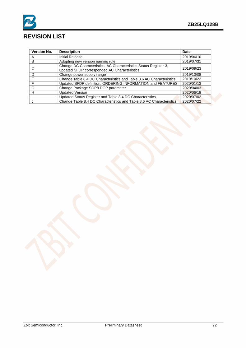
Zbit Semiconductor, Inc. Preliminary Datasheet 72
ZB25LQ128B
REVISION LIST
Version No. Description Date
A Initial Release 2019/06/10
B Adopting new version naming rule 2019/07/31
C Change DC Characteristics, AC Characteristics,Status Register-3, updated SFDP corresponded AC Characteristics 2019/09/23
D Change power supply range 2019/10/08
E Change Table 8.4 DC Characteristics and Table 8.6 AC Characteristics 2019/10/22
F Updated SFDP definition, ORDERING INFORMATION and FEATURES 2020/01/13
G Change Package SOP8 DOP parameter 2020/04/03
H Updated Version 2020/06/19
I Updated Status Register and Table 8.4 DC Characteristics 2020/07/02
J Change Table 8.4 DC Characteristics and Table 8.6 AC Characteristics 2020/07/22