182.092 computer architecture chapter 5: memory hierarchy · 182.092 computer architecture chapter...
TRANSCRIPT
182.092 Chapter 5.1 Herbert Grünbacher, TU Vienna, 2010
182.092 Computer Architecture
Chapter 5: Memory Hierarchy
Adapted from Computer Organization and Design, 4th Edition,
Patterson & Hennessy, © 2008, Morgan Kaufmann Publishersand
Mary Jane Irwin (www.cse.psu.edu/research/mdl/mji)
182.092 Chapter 5.2 Herbert Grünbacher, TU Vienna, 2010
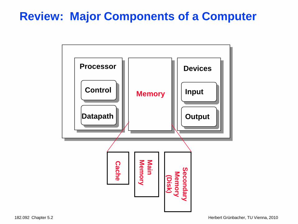
Review: Major Components of a Computer
Processor
Control
Datapath
Memory
Devices
Input
Output
Cache
Main
Mem
ory
Secondary M
emory
(Disk)

182.092 Chapter 5.4 Herbert Grünbacher, TU Vienna, 2010
The “Memory Wall” Processor vs DRAM speed disparity continues to grow
0.01
0.1
1
10
100
1000
VAX/1980 PPro/1996 2010+
CoreMemory
Clo
cks
per i
nstru
ctio
n
Clo
cks
per D
RAM
acc
ess
Good memory hierarchy (cache) design is increasingly important to overall performance
182.092 Chapter 5.5 Herbert Grünbacher, TU Vienna, 2010
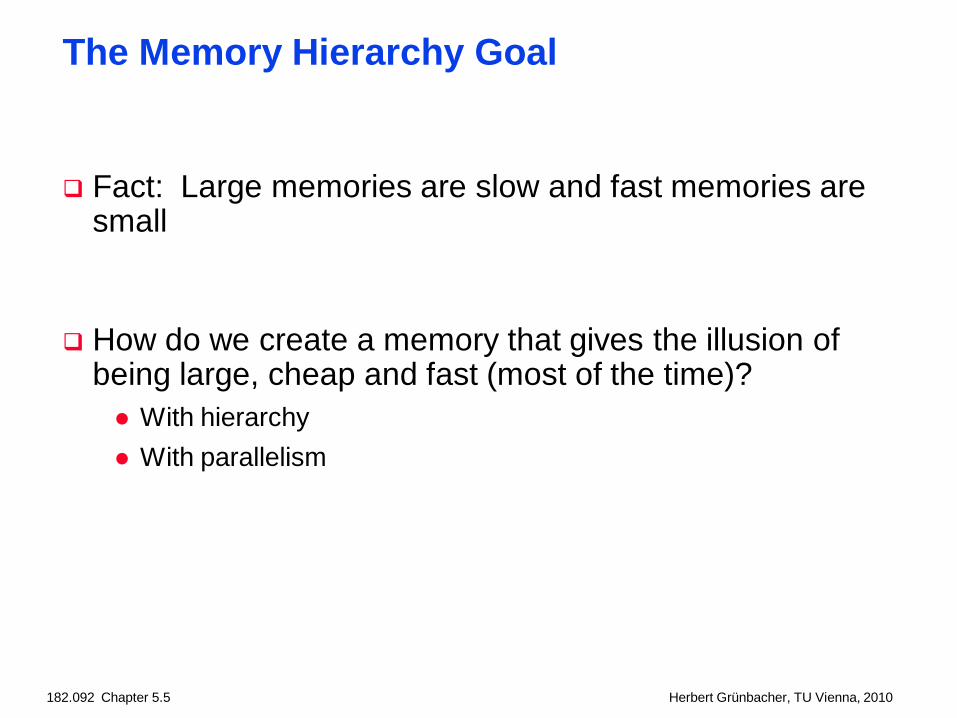
The Memory Hierarchy Goal
Fact: Large memories are slow and fast memories are small
How do we create a memory that gives the illusion of being large, cheap and fast (most of the time)? With hierarchy With parallelism

182.092 Chapter 5.6 Herbert Grünbacher, TU Vienna, 2010
SecondLevelCache
(SRAM)
A Typical Memory Hierarchy
Control
Datapath
SecondaryMemory(Disk)
On-Chip Components
RegFile
MainMemory(DRAM)D
ataC
acheInstr
Cache
ITLBD
TLB
Speed (%cycles): ½’s 1’s 10’s 100’s 10,000’s
Size (bytes): 100’s 10K’s M’s G’s T’s
Cost: highest lowest
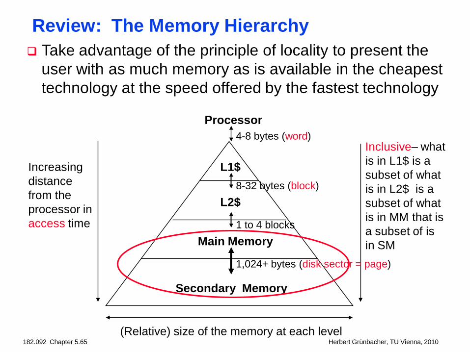
Take advantage of the principle of locality to present the user with as much memory as is available in the cheapest technology at the speed offered by the fastesttechnology
182.092 Chapter 5.7 Herbert Grünbacher, TU Vienna, 2010
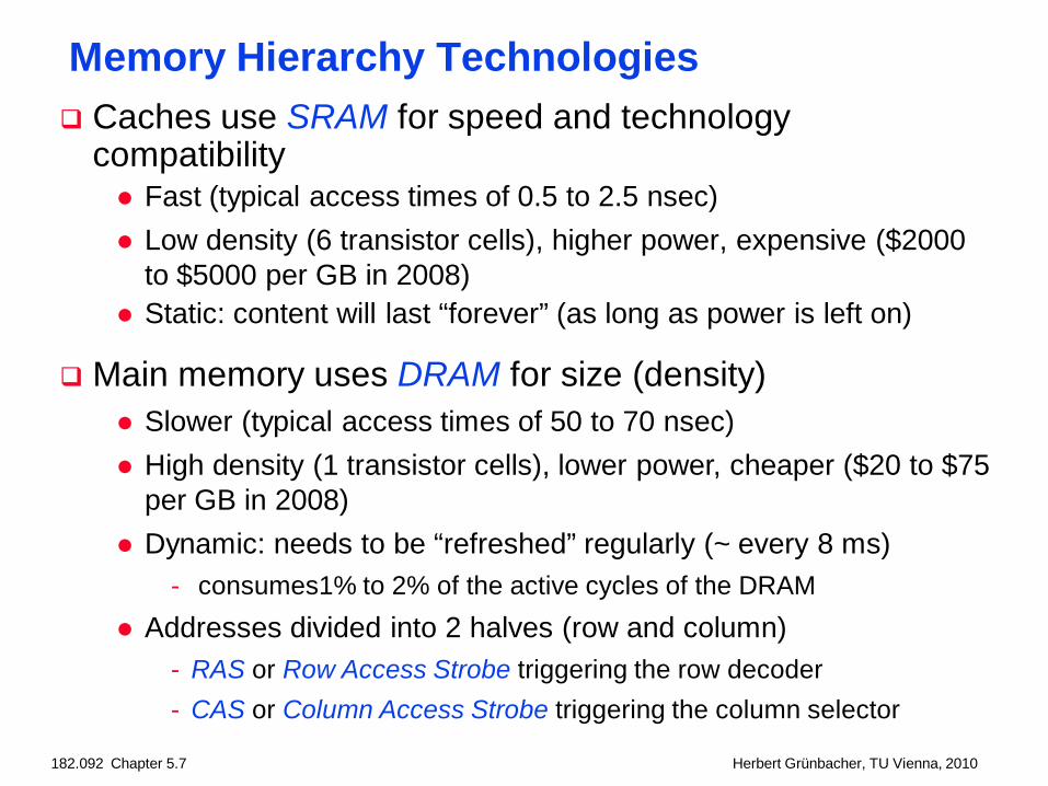
Memory Hierarchy Technologies Caches use SRAM for speed and technology
compatibility Fast (typical access times of 0.5 to 2.5 nsec) Low density (6 transistor cells), higher power, expensive ($2000
to $5000 per GB in 2008) Static: content will last “forever” (as long as power is left on)
Main memory uses DRAM for size (density) Slower (typical access times of 50 to 70 nsec) High density (1 transistor cells), lower power, cheaper ($20 to $75
per GB in 2008) Dynamic: needs to be “refreshed” regularly (~ every 8 ms)
- consumes1% to 2% of the active cycles of the DRAM Addresses divided into 2 halves (row and column)
- RAS or Row Access Strobe triggering the row decoder- CAS or Column Access Strobe triggering the column selector
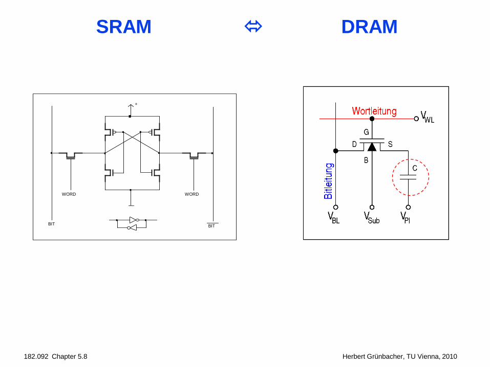
182.092 Chapter 5.8 Herbert Grünbacher, TU Vienna, 2010
SRAM DRAM
+
WORD WORD
. .
...
. .
.
BIT BIT. .

182.092 Chapter 5.9 Herbert Grünbacher, TU Vienna, 2010
The Memory Hierarchy: Why Does it Work?
Temporal Locality (locality in time) If a memory location is referenced then it will tend to be
referenced again soon⇒ Keep most recently accessed data items closer to the processor
Spatial Locality (locality in space) If a memory location is referenced, the locations with nearby
addresses will tend to be referenced soon⇒ Move blocks consisting of contiguous words closer to the
processor

182.092 Chapter 5.10 Herbert Grünbacher, TU Vienna, 2010
The Memory Hierarchy: Terminology Block (or line): the minimum unit of information that is
present (or not) in a cache Hit Rate: the fraction of memory accesses found in a level
of the memory hierarchy Hit Time: Time to access that level which consists of
Time to access the block + Time to determine hit/miss
Miss Rate: the fraction of memory accesses not found in a level of the memory hierarchy ⇒ 1 - (Hit Rate) Miss Penalty: Time to replace a block in that level with the
corresponding block from a lower level which consists ofTime to access the block in the lower level + Time to transmit that block to the level that experienced the miss + Time to insert the block in that level + Time to pass the block to the requestor
Hit Time << Miss Penalty

182.092 Chapter 5.11 Herbert Grünbacher, TU Vienna, 2010
Characteristics of the Memory Hierarchy
Increasing distance from the processor in accesstime
L1$
L2$
Main Memory
Secondary Memory
Processor
(Relative) size of the memory at each level
Inclusive–what is in L1$ is a subset of what is in L2$ is a subset of what is in MM that is a subset of is in SM
4-8 bytes (word)
1 to 4 blocks
1,024+ bytes (disk sector = page)
8-32 bytes (block)

182.092 Chapter 5.12 Herbert Grünbacher, TU Vienna, 2010
»Geographical« distances
register file
on-chip cache
on-board cache
main memory
1 m
2 m
10 m
100 m
on your desk
in your desk
in your room
in the house
disk 1000 km abroad
182.092 Chapter 5.13 Herbert Grünbacher, TU Vienna, 2010
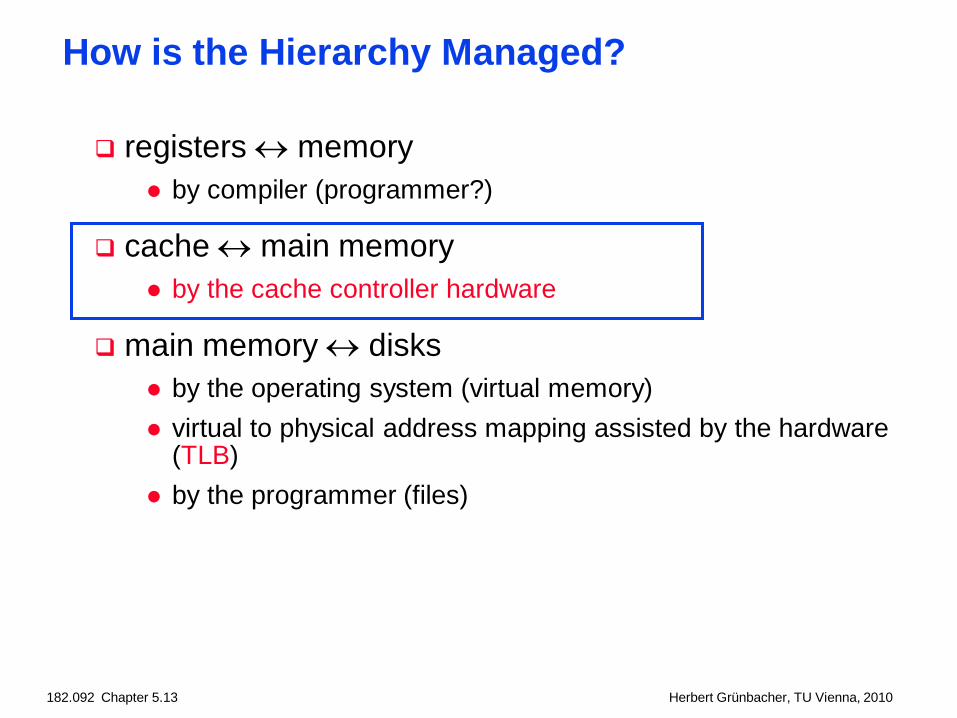
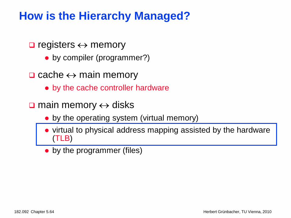
How is the Hierarchy Managed?
registers ↔ memory by compiler (programmer?)
cache ↔ main memory by the cache controller hardware
main memory ↔ disks by the operating system (virtual memory) virtual to physical address mapping assisted by the hardware
(TLB) by the programmer (files)
182.092 Chapter 5.14 Herbert Grünbacher, TU Vienna, 2010
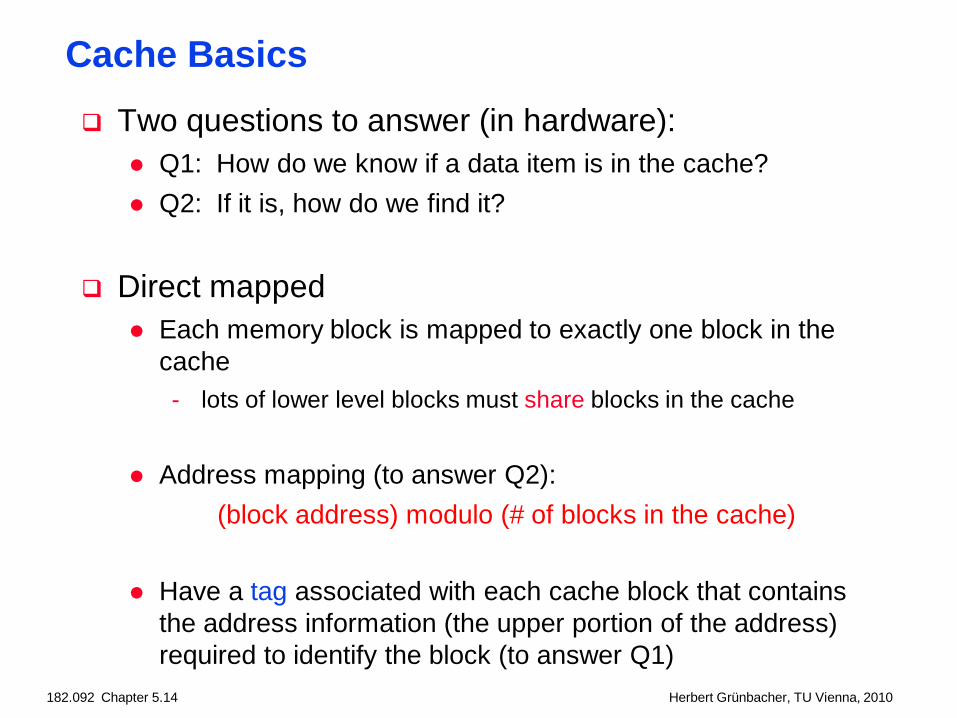
Two questions to answer (in hardware): Q1: How do we know if a data item is in the cache? Q2: If it is, how do we find it?
Direct mapped Each memory block is mapped to exactly one block in the
cache- lots of lower level blocks must share blocks in the cache
Address mapping (to answer Q2):(block address) modulo (# of blocks in the cache)
Have a tag associated with each cache block that contains the address information (the upper portion of the address) required to identify the block (to answer Q1)
Cache Basics

182.092 Chapter 5.16 Herbert Grünbacher, TU Vienna, 2010
Caching: A Simple First Example
00011011
Cache
Main Memory
Q2: How do we find it?
Use next 2 low order memory address bits – the index – to determine which cache block (i.e., modulo the number of blocks in the cache)
Tag Data
Q1: Is it there?
Compare the cache tag to the high order 2 memory address bits to tell if the memory block is in the cache
Valid
0000xx0001xx0010xx0011xx0100xx0101xx0110xx0111xx1000xx1001xx1010xx1011xx1100xx1101xx1110xx1111xx
One word blocksTwo low order bits define the byte in the word (32b words)
(block address) modulo (# of blocks in the cache)
Index

182.092 Chapter 5.18 Herbert Grünbacher, TU Vienna, 2010
Direct Mapped Cache
0 1 2 3
4 3 4 15
Consider the main memory word reference string0 1 2 3 4 3 4 15
00 Mem(0) 00 Mem(0)00 Mem(1)
00 Mem(0) 00 Mem(0)00 Mem(1)00 Mem(2)
miss miss miss miss
miss misshit hit
00 Mem(0)00 Mem(1)00 Mem(2)00 Mem(3)
01 Mem(4)00 Mem(1)00 Mem(2)00 Mem(3)
01 Mem(4)00 Mem(1)00 Mem(2)00 Mem(3)
01 Mem(4)00 Mem(1)00 Mem(2)00 Mem(3)
01 4
11 15
00 Mem(1)00 Mem(2)
00 Mem(3)
Start with an empty cache - all blocks initially marked as not valid
8 requests, 6 misses

182.092 Chapter 5.19 Herbert Grünbacher, TU Vienna, 2010
One word blocks, cache size = 1K words (or 4KB)MIPS Direct Mapped Cache Example
20Tag 10Index
DataIndex TagValid012...
102110221023
31 30 . . . 13 12 11 . . . 2 1 0Byte offset
What kind of locality are we taking advantage of?
20
Data
32
Hit

182.092 Chapter 5.20 Herbert Grünbacher, TU Vienna, 2010
Multiword Block Direct Mapped Cache
8Index
DataIndex TagValid012...
253254255
31 30 . . . 13 12 11 . . . 4 3 2 1 0 Byte offset
20
20Tag
Hit Data
32
Block offset
Four words/block, cache size = 1K words
What kind of locality are we taking advantage of?

182.092 Chapter 5.22 Herbert Grünbacher, TU Vienna, 2010
Taking Advantage of Spatial Locality
0
Let cache block hold more than one word0 1 2 3 4 3 4 15
1 2
3 4 3
4 15
00 Mem(1) Mem(0)
miss
00 Mem(1) Mem(0)
hit
00 Mem(3) Mem(2)00 Mem(1) Mem(0)
miss
hit
00 Mem(3) Mem(2)00 Mem(1) Mem(0)
miss
00 Mem(3) Mem(2)00 Mem(1) Mem(0)
01 5 4hit
00 Mem(3) Mem(2)01 Mem(5) Mem(4)
hit
00 Mem(3) Mem(2)01 Mem(5) Mem(4)
00 Mem(3) Mem(2)01 Mem(5) Mem(4)
miss
11 15 14
Start with an empty cache - all blocks initially marked as not valid
8 requests, 4 misses

182.092 Chapter 5.23 Herbert Grünbacher, TU Vienna, 2010
Miss Rate vs Block Size vs Cache Size
0
5
10
16 32 64 128 256
Mis
s ra
te (%
)
Block size (bytes)
8 KB16 KB64 KB256 KB
Miss rate goes up if the block size becomes a significant fraction of the cache size because the number of blocks that can be held in the same size cache is smaller (increasing capacity misses)
182.092 Chapter 5.24 Herbert Grünbacher, TU Vienna, 2010
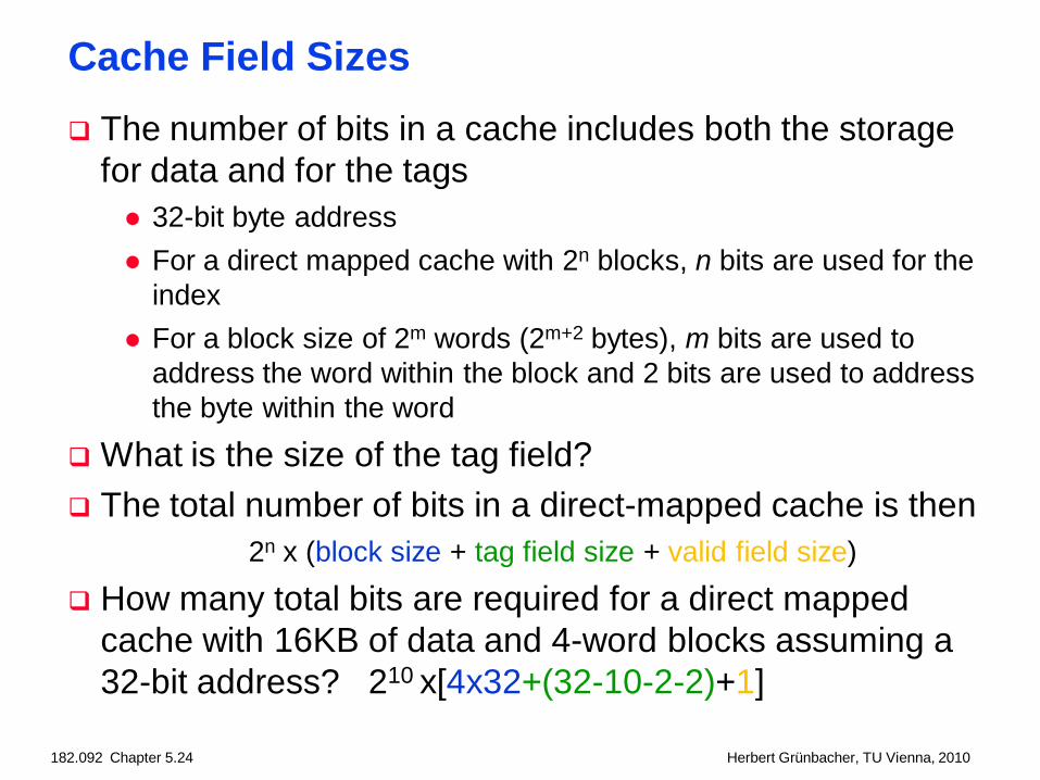
Cache Field Sizes The number of bits in a cache includes both the storage
for data and for the tags 32-bit byte address For a direct mapped cache with 2n blocks, n bits are used for the
index For a block size of 2m words (2m+2 bytes), m bits are used to
address the word within the block and 2 bits are used to address the byte within the word
What is the size of the tag field? The total number of bits in a direct-mapped cache is then
2n x (block size + tag field size + valid field size)
How many total bits are required for a direct mapped cache with 16KB of data and 4-word blocks assuming a 32-bit address? 210 x[4x32+(32-10-2-2)+1]

182.092 Chapter 5.25 Herbert Grünbacher, TU Vienna, 2010
Read hits (I$ and D$) this is what we want!
Write hits (D$ only) require the cache and memory to be consistent
- always write the data into both the cache block and the next level in the memory hierarchy (write-through)
- writes run at the speed of the next level in the memory hierarchy – so slow! – or can use a write buffer and stall only if the write buffer is full
allow cache and memory to be inconsistent- write the data only into the cache block (write-back the cache block to
the next level in the memory hierarchy when that cache block is “evicted”)
- need a dirty bit for each data cache block to tell if it needs to be written back to memory when it is evicted – can use a write buffer to help “buffer” write-backs of dirty blocks
Handling Cache Hits

182.092 Chapter 5.26 Herbert Grünbacher, TU Vienna, 2010
Sources of Cache Misses Compulsory (cold start or process migration, first
reference): First access to a block, “cold” fact of life, not a whole lot you
can do about it. If you are going to run “millions” of instructions, compulsory misses are insignificant
Solution: increase block size (increases miss penalty; very large blocks could increase miss rate)
Capacity: Cache cannot contain all blocks accessed by the program Solution: increase cache size (may increase access time)
Conflict (collision): Multiple memory locations mapped to the same cache location Solution 1: increase cache size Solution 2: increase associativity (stay tuned) (may increase
access time)
182.092 Chapter 5.27 Herbert Grünbacher, TU Vienna, 2010
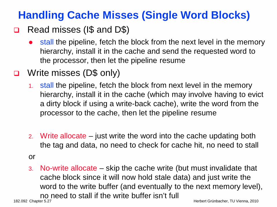
Handling Cache Misses (Single Word Blocks) Read misses (I$ and D$)
stall the pipeline, fetch the block from the next level in the memory hierarchy, install it in the cache and send the requested word to the processor, then let the pipeline resume
Write misses (D$ only)1. stall the pipeline, fetch the block from next level in the memory
hierarchy, install it in the cache (which may involve having to evict a dirty block if using a write-back cache), write the word from the processor to the cache, then let the pipeline resume
2. Write allocate – just write the word into the cache updating both the tag and data, no need to check for cache hit, no need to stall
or3. No-write allocate – skip the cache write (but must invalidate that
cache block since it will now hold stale data) and just write the word to the write buffer (and eventually to the next memory level), no need to stall if the write buffer isn’t full

182.092 Chapter 5.28 Herbert Grünbacher, TU Vienna, 2010
Multiword Block Considerations Read misses (I$ and D$)
Processed the same as for single word blocks – a miss returns the entire block from memory
Miss penalty grows as block size grows- Early restart – processor resumes execution as soon as the
requested word of the block is returned- Requested word first – requested word is transferred from the
memory to the cache (and processor) first Nonblocking cache – allows the processor to continue to access
the cache while the cache is handling an earlier miss
Write misses (D$) If using write allocate must first fetch the block from memory and
then write the word to the block
182.092 Chapter 5.29 Herbert Grünbacher, TU Vienna, 2010
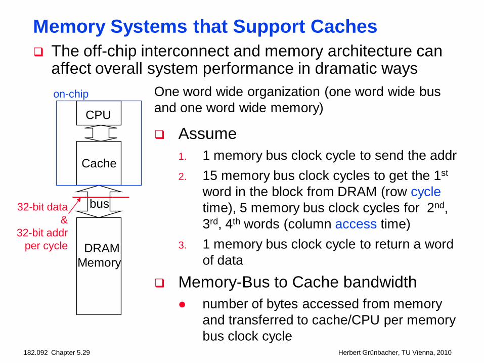
The off-chip interconnect and memory architecture can affect overall system performance in dramatic ways
Memory Systems that Support Caches
CPU
Cache
DRAMMemory
bus
One word wide organization (one word wide bus and one word wide memory)
Assume1. 1 memory bus clock cycle to send the addr2. 15 memory bus clock cycles to get the 1st
word in the block from DRAM (row cycletime), 5 memory bus clock cycles for 2nd, 3rd, 4th words (column access time)
3. 1 memory bus clock cycle to return a word of data
Memory-Bus to Cache bandwidth number of bytes accessed from memory
and transferred to cache/CPU per memory bus clock cycle
32-bit data&
32-bit addrper cycle
on-chip

182.092 Chapter 5.30 Herbert Grünbacher, TU Vienna, 2010
Review: (DDR) SDRAM Operation
N ro
ws
N cols
DRAM
ColumnAddress
M-bit OutputM bit planes
N x M SRAM
RowAddress
After a row is read into the SRAM register Input CAS as the starting “burst”
address along with a burst length Transfers a burst of data (ideally
a cache block) from a series of sequential addr’s within that row
- The memory bus clock controls transfer of successive words in the burst
+1
Row Address
CAS
RAS
Col Address
1st M-bit Access 2nd M-bit 3rd M-bit 4th M-bit
Cycle Time
Row Add

182.092 Chapter 5.33 Herbert Grünbacher, TU Vienna, 2010
One Word Wide Bus, One Word Blocks
CPU
Cache
DRAMMemory
bus
on-chip If the block size is one word, then for a
memory access due to a cache miss, the pipeline will have to stall for the number of cycles required to return one data word from memory
memory bus clock cycle to send addressmemory bus clock cycles to read DRAMmemory bus clock cycle to return datatotal clock cycles miss penalty
Number of bytes transferred per clock cycle (bandwidth) for a single miss is
bytes per memory bus clock cycle
1 151
17
4/17 = 0.235
182.092 Chapter 5.35 Herbert Grünbacher, TU Vienna, 2010
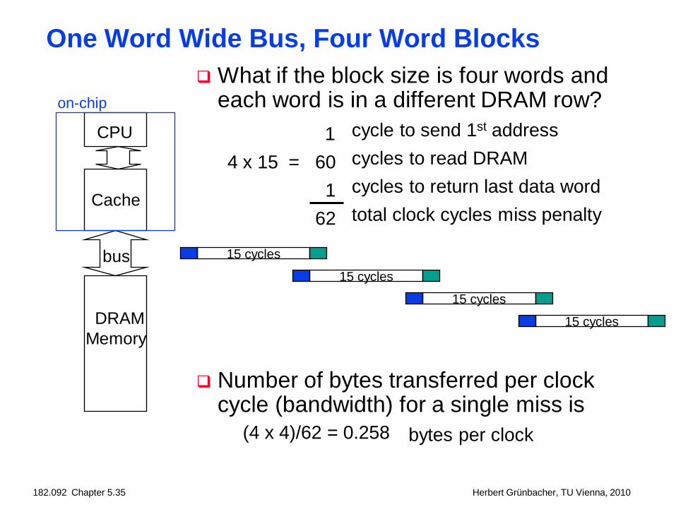
One Word Wide Bus, Four Word Blocks
CPU
Cache
DRAMMemory
bus
on-chip
What if the block size is four words and each word is in a different DRAM row?
cycle to send 1st addresscycles to read DRAMcycles to return last data wordtotal clock cycles miss penalty
Number of bytes transferred per clock cycle (bandwidth) for a single miss is
bytes per clock
15 cycles
15 cycles
15 cycles
15 cycles
14 x 15 = 60
1 62
(4 x 4)/62 = 0.258

182.092 Chapter 5.37 Herbert Grünbacher, TU Vienna, 2010
One Word Wide Bus, Four Word Blocks
CPU
Cache
DRAMMemory
bus
on-chip
What if the block size is four words and all words are in the same DRAM row?
cycle to send 1st addresscycles to read DRAMcycles to return last data wordtotal clock cycles miss penalty
Number of bytes transferred per clock cycle (bandwidth) for a single miss is
bytes per clock
15 cycles
5 cycles
5 cycles
5 cycles
1
15 + 3*5 = 301
32
(4 x 4)/32 = 0.5

182.092 Chapter 5.39 Herbert Grünbacher, TU Vienna, 2010
Interleaved Memory, One Word Wide Bus For a block size of four words
cycle to send 1st addresscycles to read DRAM bankscycles to return last data wordtotal clock cycles miss penalty
CPU
Cache
bus
on-chip
Number of bytes transferred per clock cycle (bandwidth) for a single miss is
bytes per clock
15 cycles
15 cycles
15 cycles
15 cycles
(4 x 4)/20 = 0.8
1
154*1 = 4
20
DRAMMemorybank 1
DRAMMemorybank 0
DRAMMemorybank 2
DRAMMemorybank 3

182.092 Chapter 5.40 Herbert Grünbacher, TU Vienna, 2010
DRAM Memory System Summary Its important to match the cache characteristics
caches access one block at a time (usually more than one word)
with the DRAM characteristics use DRAMs that support fast multiple word accesses,
preferably ones that match the block size of the cache
with the memory-bus characteristics make sure the memory-bus can support the DRAM access
rates and patterns with the goal of increasing the Memory-Bus to Cache
bandwidth

182.092 Chapter 5.41 Herbert Grünbacher, TU Vienna, 2010
Measuring Cache Performance Assuming cache hit costs are included as part of the
normal CPU execution cycle, thenCPU time = IC CPI CC
= IC (CPIideal + Memory-stall cycles) CC
CPIstall
Memory-stall cycles come from cache misses (a sum of read-stalls and write-stalls)
Read-stall cycles = reads/program read miss rate read miss penalty
Write-stall cycles = (writes/program write miss rate write miss penalty)
+ write buffer stalls
For write-through caches, we can simplify this toMemory-stall cycles = accesses/program miss rate miss penalty

182.092 Chapter 5.42 Herbert Grünbacher, TU Vienna, 2010
Impacts of Cache Performance Relative cache penalty increases as processor
performance improves (faster clock rate and/or lower CPI) The memory speed is unlikely to improve as fast as processor
cycle time. When calculating CPIstall, the cache miss penalty is measured in processor clock cycles needed to handle a miss
The lower the CPIideal, the more pronounced the impact of stalls
A processor with a CPIideal of 2, a 100 cycle miss penalty, 36% load/store instr’s, and 2% I$ and 4% D$ miss rates
Memory-stall cycles = 2% 100 + 36% 4% 100 = 3.44So CPIstalls = 2 + 3.44 = 5.44
more than twice the CPIideal ! What if the CPIideal is reduced to 1? 0.5? 0.25? What if the D$ miss rate went up 1%? 2%? What if the processor clock rate is doubled (doubling the
miss penalty)?

182.092 Chapter 5.43 Herbert Grünbacher, TU Vienna, 2010
Average Memory Access Time (AMAT) A larger cache will have a longer access time. An
increase in hit time will likely add another stage to the pipeline
Average Memory Access Time (AMAT) is the average to access memory considering both hits and misses
AMAT = Time for a hit + Miss rate x Miss penalty
What is the AMAT for a processor with a 20 psec clock, a miss penalty of 50 clock cycles, a miss rate of 0.02 misses per instruction and a cache access time of 1 clock cycle?

182.092 Chapter 5.44 Herbert Grünbacher, TU Vienna, 2010
Reducing Cache Miss Rates #11. Allow more flexible block placement
In a direct mapped cache a memory block maps to exactly one cache block
At the other extreme, could allow a memory block to be mapped to any cache block – fully associative cache
A compromise is to divide the cache into sets each of which consists of n “ways” (n-way set associative). A memory block maps to a unique set (specified by the index field) and can be placed in any way of that set (so there are n choices)
(block address) modulo (# sets in the cache)
182.092 Chapter 5.46 Herbert Grünbacher, TU Vienna, 2010
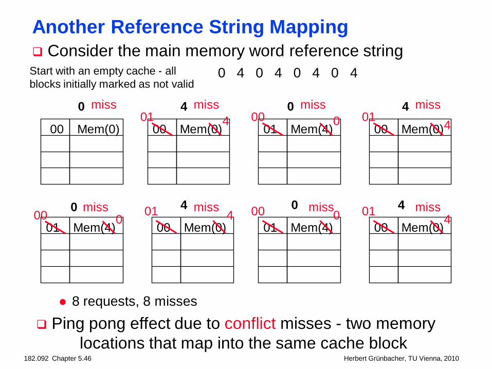
Another Reference String Mapping
0 4 0 4
0 4 0 4
Consider the main memory word reference string0 4 0 4 0 4 0 4
miss miss miss miss
miss miss miss miss
00 Mem(0) 00 Mem(0)01 4
01 Mem(4)000
00 Mem(0)01
4
00 Mem(0)01 4
00 Mem(0)01
401 Mem(4)
00001 Mem(4)
000
Start with an empty cache - all blocks initially marked as not valid
Ping pong effect due to conflict misses - two memory locations that map into the same cache block
8 requests, 8 misses

182.092 Chapter 5.47 Herbert Grünbacher, TU Vienna, 2010
Set Associative Cache Example
0
Cache
Main Memory
Q2: How do we find it?
Use next 1 low order memory address bit to determine which cache set (i.e., modulo the number of sets in the cache)
Tag Data
Q1: Is it there?
Compare all the cache tags in the set to the high order 3 memory address bits to tell if the memory block is in the cache
V
0000xx0001xx0010xx0011xx0100xx0101xx0110xx0111xx1000xx1001xx1010xx1011xx1100xx1101xx1110xx1111xx
Set
1
01
Way
0
1
One word blocksTwo low order bits define the byte in the word (32b words)

182.092 Chapter 5.49 Herbert Grünbacher, TU Vienna, 2010
Another Reference String Mapping
0 4 0 4
Consider the main memory word reference string0 4 0 4 0 4 0 4
miss miss hit hit
000 Mem(0) 000 Mem(0)
Start with an empty cache - all blocks initially marked as not valid
010 Mem(4) 010 Mem(4)
000 Mem(0) 000 Mem(0)
010 Mem(4)
Solves the ping pong effect in a direct mapped cache due to conflict misses since now two memory locations that map into the same cache set can co-exist!
8 requests, 2 misses

182.092 Chapter 5.50 Herbert Grünbacher, TU Vienna, 2010
Four-Way Set Associative Cache 28 = 256 sets each with four ways (each with one block)
31 30 . . . 13 12 11 . . . 2 1 0 Byte offset
DataTagV012...
253254255
DataTagV012...
253254255
DataTagV012...
253254255
Index DataTagV012...
253254255
8Index
22Tag
Hit Data
32
4x1 select
Way 0 Way 1 Way 2 Way 3
182.092 Chapter 5.52 Herbert Grünbacher, TU Vienna, 2010
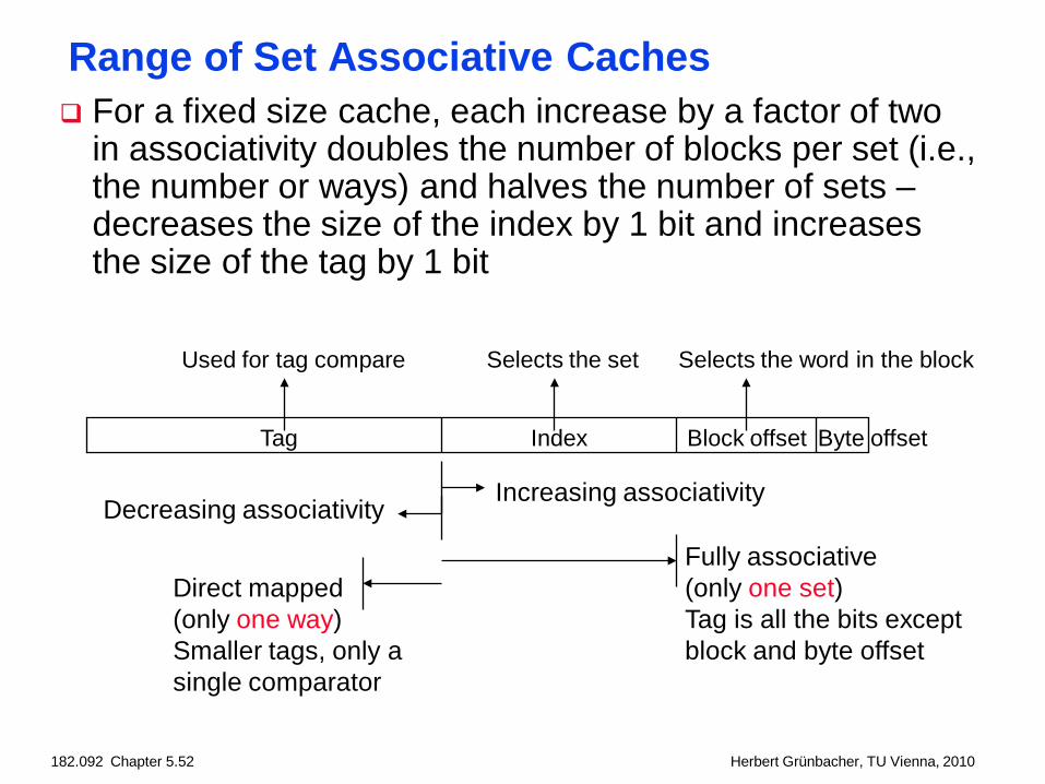
Range of Set Associative Caches For a fixed size cache, each increase by a factor of two
in associativity doubles the number of blocks per set (i.e., the number or ways) and halves the number of sets –decreases the size of the index by 1 bit and increases the size of the tag by 1 bit
Block offset Byte offsetIndexTag
Decreasing associativity
Fully associative(only one set)Tag is all the bits exceptblock and byte offset
Direct mapped(only one way)Smaller tags, only a single comparator
Increasing associativity
Selects the setUsed for tag compare Selects the word in the block
182.092 Chapter 5.53 Herbert Grünbacher, TU Vienna, 2010
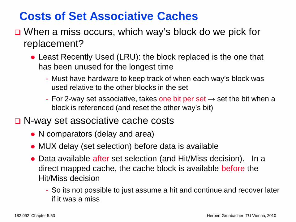
Costs of Set Associative Caches When a miss occurs, which way’s block do we pick for
replacement? Least Recently Used (LRU): the block replaced is the one that
has been unused for the longest time- Must have hardware to keep track of when each way’s block was
used relative to the other blocks in the set- For 2-way set associative, takes one bit per set → set the bit when a
block is referenced (and reset the other way’s bit)
N-way set associative cache costs N comparators (delay and area) MUX delay (set selection) before data is available Data available after set selection (and Hit/Miss decision). In a
direct mapped cache, the cache block is available before the Hit/Miss decision
- So its not possible to just assume a hit and continue and recover later if it was a miss

182.092 Chapter 5.54 Herbert Grünbacher, TU Vienna, 2010
Benefits of Set Associative Caches The choice of direct mapped or set associative depends
on the cost of a miss versus the cost of implementation
0
2
4
6
8
10
12
1-way 2-way 4-way 8-wayAssociativity
Mis
s R
ate
4KB8KB16KB32KB64KB128KB256KB512KB
Data from Hennessy & Patterson, Computer Architecture, 2003
Largest gains are in going from direct mapped to 2-way (20%+ reduction in miss rate)

182.092 Chapter 5.55 Herbert Grünbacher, TU Vienna, 2010
Reducing Cache Miss Rates #22. Use multiple levels of caches
With advancing technology have more than enough room on the die for bigger L1 caches or for a second level of caches – normally a unified L2 cache (i.e., it holds both instructions and data) and in some cases even a unified L3 cache
For our example, CPIideal of 2, 100 cycle miss penalty (to main memory) and a 25 cycle miss penalty (to UL2$), 36% load/stores, a 2% (4%) L1 I$ (D$) miss rate, add a 0.5% UL2$ miss rate
CPIstalls = 2 + .02 25 + .36 .04 25 + .005 100 + .36 .005 100 = 3.54 (as compared to 5.44 with no L2$)

182.092 Chapter 5.56 Herbert Grünbacher, TU Vienna, 2010
Multilevel Cache Design Considerations Design considerations for L1 and L2 caches are very
different Primary cache should focus on minimizing hit time in support of
a shorter clock cycle- Smaller with smaller block sizes
Secondary cache(s) should focus on reducing miss rate to reduce the penalty of long main memory access times
- Larger with larger block sizes- Higher levels of associativity
The miss penalty of the L1 cache is significantly reduced by the presence of an L2 cache – so it can be smaller (i.e., faster) but have a higher miss rate
For the L2 cache, hit time is less important than miss rate The L2$ hit time determines L1$’s miss penalty L2$ local miss rate >> than the global miss rate
182.092 Chapter 5.57 Herbert Grünbacher, TU Vienna, 2010
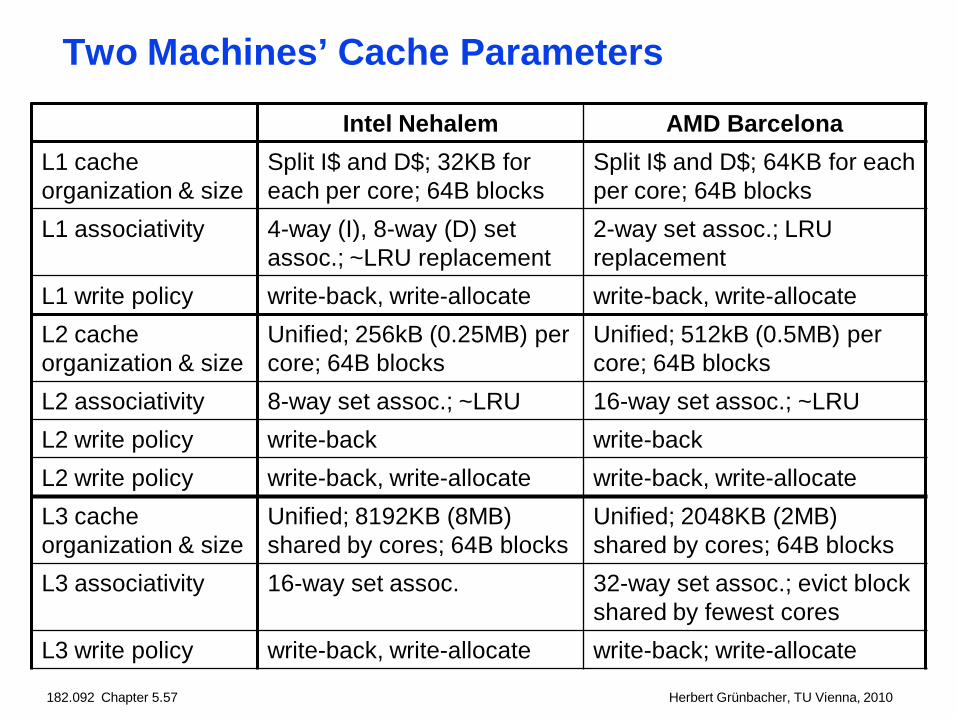
Two Machines’ Cache Parameters
Intel Nehalem AMD BarcelonaL1 cache organization & size
Split I$ and D$; 32KB for each per core; 64B blocks
Split I$ and D$; 64KB for each per core; 64B blocks
L1 associativity 4-way (I), 8-way (D) set assoc.; ~LRU replacement
2-way set assoc.; LRU replacement
L1 write policy write-back, write-allocate write-back, write-allocateL2 cache organization & size
Unified; 256kB (0.25MB) per core; 64B blocks
Unified; 512kB (0.5MB) per core; 64B blocks
L2 associativity 8-way set assoc.; ~LRU 16-way set assoc.; ~LRUL2 write policy write-back write-backL2 write policy write-back, write-allocate write-back, write-allocateL3 cache organization & size
Unified; 8192KB (8MB) shared by cores; 64B blocks
Unified; 2048KB (2MB) shared by cores; 64B blocks
L3 associativity 16-way set assoc. 32-way set assoc.; evict block shared by fewest cores
L3 write policy write-back, write-allocate write-back; write-allocate

182.092 Chapter 5.59 Herbert Grünbacher, TU Vienna, 2010
Cache Coherence in Multicores In future multicore processors its likely that the cores will
share a common physical address space, causing a cache coherence problem
There are many variations on cache coherence protocols
Hennessy & Patterson, Computer Architecture: A Quantitative Approach

182.092 Chapter 5.60 Herbert Grünbacher, TU Vienna, 2010
Summary: Improving Cache Performance0. Reduce the time to hit in the cache
smaller cache direct mapped cache smaller blocks for writes
- no write allocate – no “hit” on cache, just write to write buffer- write allocate – to avoid two cycles (first check for hit, then write)
pipeline writes via a delayed write buffer to cache
1. Reduce the miss rate bigger cache more flexible placement (increase associativity) larger blocks (16 to 64 bytes typical) victim cache – small buffer holding most recently discarded blocks
182.092 Chapter 5.61 Herbert Grünbacher, TU Vienna, 2010
Summary: Improving Cache Performance2. Reduce the miss penalty
smaller blocks use a write buffer to hold dirty blocks being replaced so don’t
have to wait for the write to complete before reading check write buffer (and/or victim cache) on read miss – may get
lucky for large blocks fetch critical word first use multiple cache levels – L2 cache not tied to CPU clock rate faster backing store/improved memory bandwidth
- wider buses- memory interleaving, DDR SDRAMs

182.092 Chapter 5.62 Herbert Grünbacher, TU Vienna, 2010
Summary: The Cache Design Space Several interacting dimensions
cache size block size associativity replacement policy write-through vs write-back write allocation
The optimal choice is a compromise depends on access characteristics
- workload- use (I-cache, D-cache, TLB)
depends on technology / cost
Simplicity often wins
Associativity
Cache Size
Block Size
Bad
Good
Less More
Factor A Factor B

182.092 Chapter 5.64 Herbert Grünbacher, TU Vienna, 2010
How is the Hierarchy Managed?
registers ↔ memory by compiler (programmer?)
cache ↔ main memory by the cache controller hardware
main memory ↔ disks by the operating system (virtual memory) virtual to physical address mapping assisted by the hardware
(TLB) by the programmer (files)
182.092 Chapter 5.65 Herbert Grünbacher, TU Vienna, 2010
Review: The Memory Hierarchy
Increasing distance from the processor in access time
L1$
L2$
Main Memory
Secondary Memory
Processor
(Relative) size of the memory at each level
Inclusive– what is in L1$ is a subset of what is in L2$ is a subset of what is in MM that is a subset of is in SM
4-8 bytes (word)
1 to 4 blocks
1,024+ bytes (disk sector = page)
8-32 bytes (block)
Take advantage of the principle of locality to present the user with as much memory as is available in the cheapest technology at the speed offered by the fastest technology

182.092 Chapter 5.66 Herbert Grünbacher, TU Vienna, 2010
Virtual Memory Use main memory as a “cache” for secondary memory
Allows efficient and safe sharing of memory among multiple programs
Provides the ability to easily run programs larger than the size of physical memory
Simplifies loading a program for execution by providing for code relocation (i.e., the code can be loaded anywhere in main memory)
What makes it work? – again the Principle of Locality A program is likely to access a relatively small portion of its
address space during any period of time
Each program is compiled into its own address space – a “virtual” address space During run-time each virtual address must be translated to a
physical address (an address in main memory)
182.092 Chapter 5.67 Herbert Grünbacher, TU Vienna, 2010
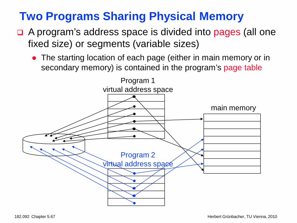
Two Programs Sharing Physical Memory
Program 1virtual address space
main memory
A program’s address space is divided into pages (all one fixed size) or segments (variable sizes) The starting location of each page (either in main memory or in
secondary memory) is contained in the program’s page table
Program 2virtual address space

182.092 Chapter 5.68 Herbert Grünbacher, TU Vienna, 2010
Address Translation
Virtual Address (VA)
Page offsetVirtual page number
31 30 . . . 12 11 . . . 0
Page offsetPhysical page number
Physical Address (PA)29 . . . 12 11 0
Translation
So each memory request first requires an address translation from the virtual space to the physical space A virtual memory miss (i.e., when the page is not in physical
memory) is called a page fault
A virtual address is translated to a physical address by a combination of hardware and software

182.092 Chapter 5.69 Herbert Grünbacher, TU Vienna, 2010
Address Translation Mechanisms
Physical pagebase addr
Main memory
Disk storage
Virtual page #
V11111101010
Page Table(in main memory)
Offset
Physical page #
Offset
Pag
e ta
ble
regi
ster

182.092 Chapter 5.70 Herbert Grünbacher, TU Vienna, 2010
Virtual Addressing with a Cache Thus it takes an extra memory access to translate a VA
to a PA
CPU Trans-lation Cache Main
Memory
VA PA miss
hitdata
This makes memory (cache) accesses very expensive (if every access was really two accesses)
The hardware fix is to use a Translation Lookaside Buffer (TLB) – a small cache that keeps track of recently used address mappings to avoid having to do a page table lookup
182.092 Chapter 5.71 Herbert Grünbacher, TU Vienna, 2010
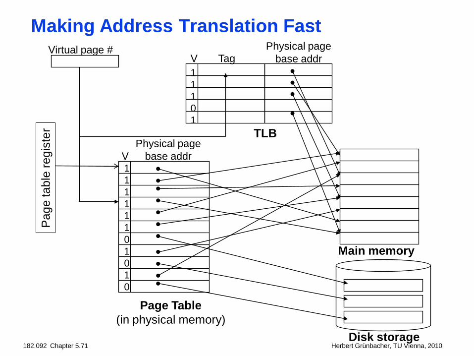
Making Address Translation Fast
Physical pagebase addr
Main memory
Disk storage
Virtual page #
V11111101010
11101
TagPhysical page
base addrV
TLB
Page Table(in physical memory)
Pag
e ta
ble
regi
ster
182.092 Chapter 5.72 Herbert Grünbacher, TU Vienna, 2010
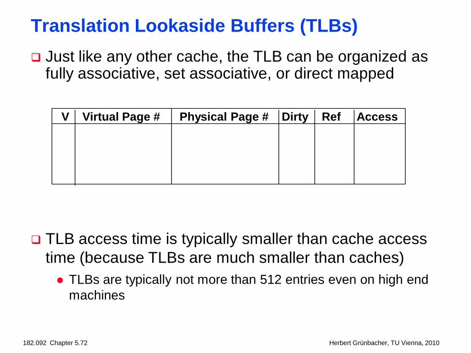
Translation Lookaside Buffers (TLBs) Just like any other cache, the TLB can be organized as
fully associative, set associative, or direct mapped
V Virtual Page # Physical Page # Dirty Ref Access
TLB access time is typically smaller than cache access time (because TLBs are much smaller than caches) TLBs are typically not more than 512 entries even on high end
machines

182.092 Chapter 5.73 Herbert Grünbacher, TU Vienna, 2010
A TLB in the Memory Hierarchy
A TLB miss – is it a page fault or merely a TLB miss? If the page is loaded into main memory, then the TLB miss can be
handled (in hardware or software) by loading the translation information from the page table into the TLB
- Takes 10’s of cycles to find and load the translation info into the TLB If the page is not in main memory, then it’s a true page fault
- Takes 1,000,000’s of cycles to service a page fault
TLB misses are much more frequent than true page faults
CPU TLBLookup Cache Main
Memory
VA PA miss
hit
data
Trans-lation
hit
miss
¾ t¼ t
182.092 Chapter 5.75 Herbert Grünbacher, TU Vienna, 2010
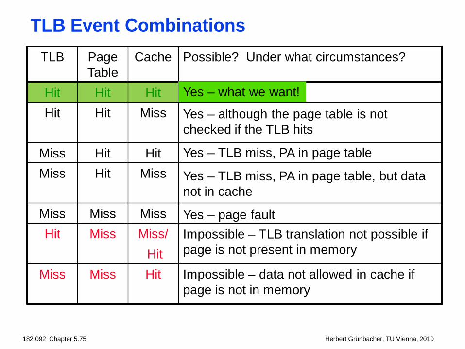
TLB Event CombinationsTLB Page
TableCache Possible? Under what circumstances?
Hit Hit HitHit Hit Miss
Miss Hit HitMiss Hit Miss
Miss Miss MissHit Miss Miss/
HitMiss Miss Hit
Yes – what we want!
Yes – although the page table is not checked if the TLB hits
Yes – TLB miss, PA in page table
Yes – TLB miss, PA in page table, but datanot in cache
Yes – page faultImpossible – TLB translation not possible ifpage is not present in memory
Impossible – data not allowed in cache if page is not in memory

182.092 Chapter 5.76 Herbert Grünbacher, TU Vienna, 2010
Handling a TLB Miss Consider a TLB miss for a page that is present in
memory (i.e., the Valid bit in the page table is set) A TLB miss (or a page fault exception) must be asserted by the
end of the same clock cycle that the memory access occurs so that the next clock cycle will begin exception processing
Register CP0 Reg # DescriptionEPC 14 Where to restart after exceptionCause 13 Cause of exceptionBadVAddr 8 Address that caused exceptionIndex 0 Location in TLB to be read/writtenRandom 1 Pseudorandom location in TLBEntryLo 2 Physical page address and flagsEntryHi 10 Virtual page addressContext 4 Page table address & page number
182.092 Chapter 5.77 Herbert Grünbacher, TU Vienna, 2010
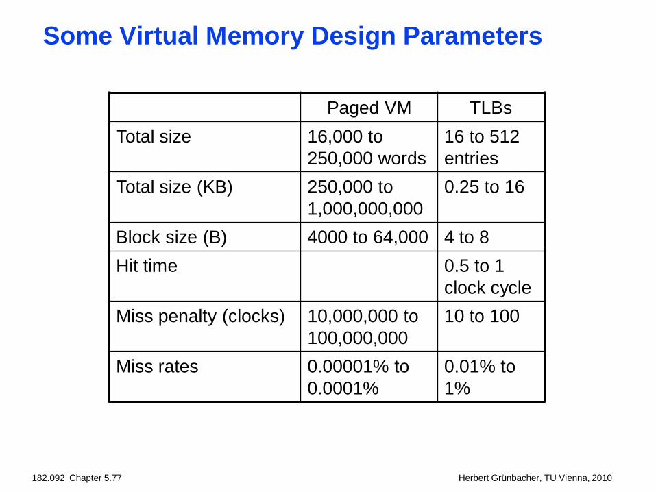
Some Virtual Memory Design Parameters
Paged VM TLBsTotal size 16,000 to
250,000 words16 to 512 entries
Total size (KB) 250,000 to 1,000,000,000
0.25 to 16
Block size (B) 4000 to 64,000 4 to 8Hit time 0.5 to 1
clock cycleMiss penalty (clocks) 10,000,000 to
100,000,00010 to 100
Miss rates 0.00001% to 0.0001%
0.01% to 1%

182.092 Chapter 5.78 Herbert Grünbacher, TU Vienna, 2010
Two Machines’ TLB ParametersIntel Nehalem AMD Barcelona
Address sizes 48 bits (vir); 44 bits (phy) 48 bits (vir); 48 bits (phy)
Page size 4KB 4KB
TLB organization L1 TLB for instructions and L1 TLB for data per core; both are 4-way set assoc.; LRUL1 ITLB has 128 entries, L2 DTLB has 64 entries
L2 TLB (unified) is 4-way set assoc.; LRU L2 TLB has 512 entries
TLB misses handled in hardware
L1 TLB for instructions and L1 TLB for data per core; both are fully assoc.; LRUL1 ITLB and DTLB each have 48 entries
L2 TLB for instructions and L2 TLB for data per core; each are 4-way set assoc.; round robin LRU Both L2 TLBs have 512 entriesTLB misses handled in hardware

182.092 Chapter 5.80 Herbert Grünbacher, TU Vienna, 2010
Why Not a Virtually Addressed Cache? A virtually addressed cache would only require address
translation on cache misses
data
CPU Trans-lation
Cache
MainMemory
VA
hit
PA
but Two programs which are sharing data will have two different
virtual addresses for the same physical address – aliasing – so have two copies of the shared data in the cache and two entries in the TBL which would lead to coherence issues
- Must update all cache entries with the same physical address or the memory becomes inconsistent
182.092 Chapter 5.81 Herbert Grünbacher, TU Vienna, 2010
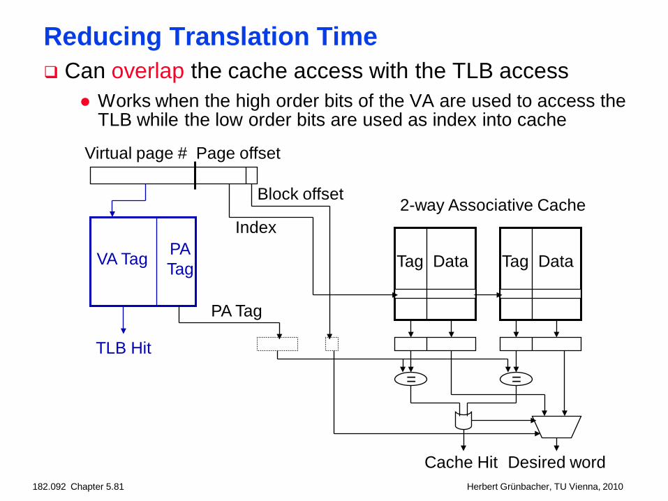
Reducing Translation Time Can overlap the cache access with the TLB access
Works when the high order bits of the VA are used to access the TLB while the low order bits are used as index into cache
Tag Data
=
Tag Data
=
Cache Hit Desired word
VA Tag PATag
TLB Hit
2-way Associative CacheIndex
PA Tag
Block offset
Page offsetVirtual page #
182.092 Chapter 5.82 Herbert Grünbacher, TU Vienna, 2010
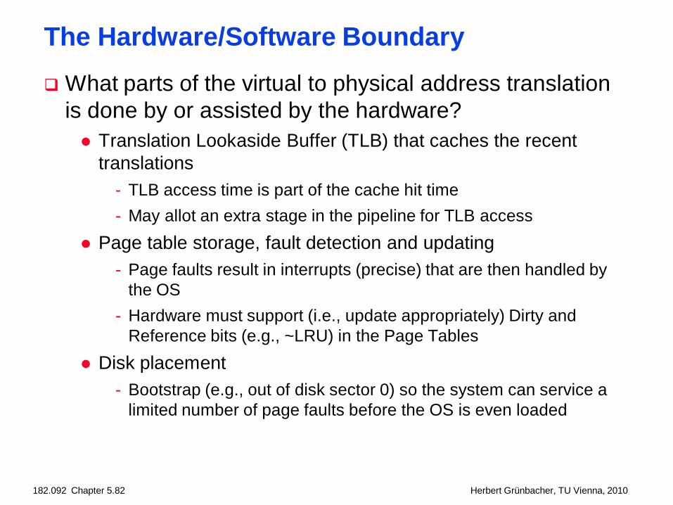
The Hardware/Software Boundary What parts of the virtual to physical address translation
is done by or assisted by the hardware? Translation Lookaside Buffer (TLB) that caches the recent
translations- TLB access time is part of the cache hit time- May allot an extra stage in the pipeline for TLB access
Page table storage, fault detection and updating- Page faults result in interrupts (precise) that are then handled by
the OS- Hardware must support (i.e., update appropriately) Dirty and
Reference bits (e.g., ~LRU) in the Page Tables Disk placement
- Bootstrap (e.g., out of disk sector 0) so the system can service a limited number of page faults before the OS is even loaded

182.092 Chapter 5.83 Herbert Grünbacher, TU Vienna, 2010
4 Questions for the Memory Hierarchy
Q1: Where can a entry be placed in the upper level? (Entry placement)
Q2: How is a entry found if it is in the upper level?(Entry identification)
Q3: Which entry should be replaced on a miss? (Entry replacement)
Q4: What happens on a write? (Write strategy)
182.092 Chapter 5.84 Herbert Grünbacher, TU Vienna, 2010
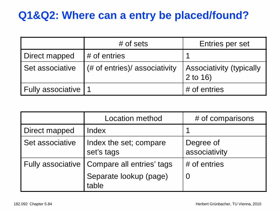
Q1&Q2: Where can a entry be placed/found?
# of sets Entries per setDirect mapped # of entries 1Set associative (# of entries)/ associativity Associativity (typically
2 to 16)Fully associative 1 # of entries
Location method # of comparisonsDirect mapped Index 1Set associative Index the set; compare
set’s tagsDegree of associativity
Fully associative Compare all entries’ tagsSeparate lookup (page) table
# of entries0
182.092 Chapter 5.85 Herbert Grünbacher, TU Vienna, 2010
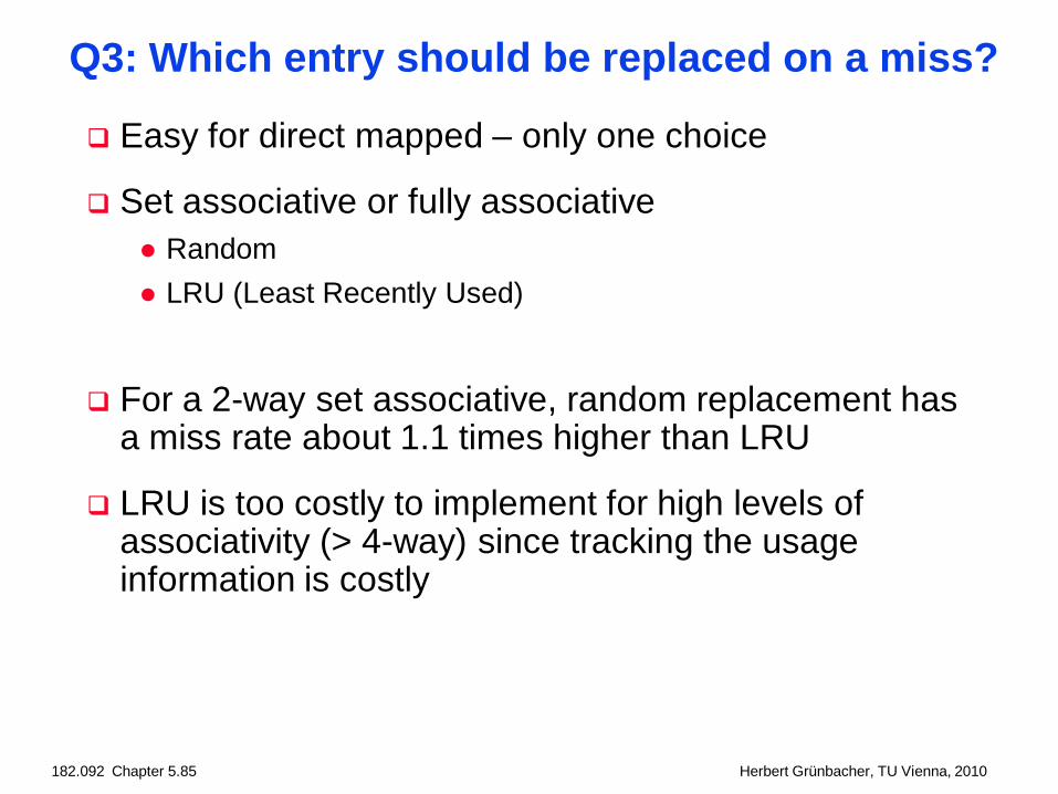
Q3: Which entry should be replaced on a miss?
Easy for direct mapped – only one choice
Set associative or fully associative Random LRU (Least Recently Used)
For a 2-way set associative, random replacement has a miss rate about 1.1 times higher than LRU
LRU is too costly to implement for high levels of associativity (> 4-way) since tracking the usage information is costly

182.092 Chapter 5.86 Herbert Grünbacher, TU Vienna, 2010
Q4: What happens on a write? Write-through – The information is written to the entry in
the current memory level and to the entry in the next level of the memory hierarchy Always combined with a write buffer so write waits to next level
memory can be eliminated (as long as the write buffer doesn’t fill)
Write-back – The information is written only to the entry in the current memory level. The modified entry is written to next level of memory only when it is replaced. Need a dirty bit to keep track of whether the entry is clean or dirty Virtual memory systems always use write-back of dirty pages to
disk
Pros and cons of each? Write-through: read misses don’t result in writes (so are simpler
and cheaper), easier to implement Write-back: writes run at the speed of the cache; repeated writes
require only one write to lower level

182.092 Chapter 5.87 Herbert Grünbacher, TU Vienna, 2010
Summary The Principle of Locality:
Program likely to access a relatively small portion of the address space at any instant of time.- Temporal Locality: Locality in Time- Spatial Locality: Locality in Space
Caches, TLBs, Virtual Memory all understood by examining how they deal with the four questions1. Where can entry be placed?2. How is entry found?3. What entry is replaced on miss?4. How are writes handled?
Page tables map virtual address to physical address TLBs are important for fast translation