1776 ieee transactions on components, · pdf filenathan neuhart, shubham jain, ......
TRANSCRIPT

1776 IEEE TRANSACTIONS ON COMPONENTS, PACKAGING AND MANUFACTURING TECHNOLOGY, VOL. 6, NO. 12, DECEMBER 2016
Ultrathin, Substrate-Integrated, and Self-HealingNanocapacitors With Low-Leakage Currents
and High-Operating FrequenciesParthasarathi Chakraborti, Himani Sharma, Markondeya Raj Pulugurtha, Kamil-Paul Rataj, Christopher Schnitter,
Nathan Neuhart, Shubham Jain, Saumya Gandhi, and Rao R. Tummala, Life Fellow, IEEE
Abstract— This paper describes ultrathin tantalum-based high-volumetric-density power capacitors with low leakage proper-ties for 1–10-MHz frequency applications. Nanodielectrics withlow-defect density were grown on nanoporous tantalum anodesusing the self-limiting anodization process. The fundamentalmechanisms that govern the film growth and quality were inves-tigated to provide anodization process guidelines. Conductingpolymer nanoparticles were used as the cathodes. Completefilling of conducting polymer was achieved by the optimizationof conducting polymer application process. Energy dispersivespectroscopy and structural SEM studies were performed toinvestigate the morphology and structure of the tantalum pen-toxide films. The fabricated capacitor showed 0.6–0.8 µF/mm2
of capacitance density in the 1–10-MHz range, in substrate-compatible ultrathin (<75 µm) form factors. This is the highestvolumetric density reported for such thin-film capacitors in amegahertz frequency range.
Index Terms— Anodization, capacitance density, highfrequency, high-surface area, leakage current, sintering, thin film.
I. INTRODUCTION
THE trend toward miniaturized electronics with higherperformance has stimulated interest in development
of affordable, compact, and integrated thin-film capacitors.Tantalum [1]–[4], MLCC [5]–[7], aluminum [8], [9],titanium [9], and trench capacitors [10], [11] are the prominent
Manuscript received May 29, 2016; accepted July 28, 2016. Date ofpublication September 20, 2016; date of current version January 6, 2017. Thiswork was supported in part by Texas Instruments, H.C. Starck GmbH, Maxim-Integrated, in part by Qualcomm, and AVX Corporation. Recommended forpublication by Associate Editor J. E. Morris upon evaluation of reviewers’comments. (Corresponding author: Parthasarathi Chakraborti.)
P. Chakraborti, H. Sharma, M. R. Pulugurtha, and R. R. Tummalaare with the 3D Systems Packaging Research Center, Geor-gia Institute of Technology, Atlanta, GA 30332 USA (e-mail:[email protected]; [email protected]; [email protected];[email protected]).
K.-P. Rataj and C. Schnitter are with H.C. Starck GmbH,38642 Goslar, Germany (e-mail: [email protected];[email protected]).
N. Neuhart is with School of Chemical and Biomolecular Engineer-ing, Georgia Institute of Technology, Atlanta, GA 30332 USA (e-mail:[email protected]).
S. Jain is with the Indian Institute of Technology Varanasi, Varanasi 221005,India (e-mail: [email protected]).
S. Gandhi is with Texas Instruments, Dallas, TX 75243 USA (e-mail:[email protected]).
Color versions of one or more of the figures in this paper are availableonline at http://ieeexplore.ieee.org.
Digital Object Identifier 10.1109/TCPMT.2016.2602213
capacitor technologies to achieve high capacitance densities.However, each of them presents process or cost limitationsin being integrated as thin-film capacitors on silicon or inpackages. Tantalum capacitors, in spite of their inherenthigh volumetric capacitance densities, come in large formfactors and are packaged as surface mount devices (SMDs)leading to large conduction pathways with lower operatingfrequencies. If they are processed as substrate-integrated thinfilms with nanostructured electrodes and dielectrics, theycan overcome the process and cost limitations and provideideal capacitor solution for integrated power modules. Thispaper focuses on developing such high volumetric densityminiaturized thin-film tantalum capacitors with stable capaci-tance at high operating frequency with low leakage currents.The use of conducting polymers as electrodes also providesself-healing function, further increasing their reliability andmanufacturability.
Electrical properties such as volumetric capacitance density,operating frequency, and equivalent series resistance (ESR),of high-density tantalum capacitors largely depend on theanode architecture, cathode conductivity, and cathode cover-age. The schematic of an SMD tantalum capacitor is shown inFig. 1(a) with manganese dioxide as cathode and carbon andsilver paste as current collector packaged inside a molded casewith lead-frame interconnections for anodes and cathodes. TheSMD capacitor yields approximately 220 μF of capacitanceat 120 Hz for 3.5 × 2.8 mm2 cross section correspondingto ∼22.4 μF/mm2 of capacitance density. Packaging con-siderations swell the form factor to 1.9 mm that limits thevolumetric capacitance density to 12 μF/mm3. Processingthem as printable nanostructured tantalum anode scales downthe geometry as well as the form factor of the anode as thedimensions can be controlled by the stencil opening and theheight. The surface-area enhancement from the anode couldbe controlled by controlling the size of the tantalum particlesin the paste and sintering conditions yielding high-surface-areaanode architecture in a very small volume leading to highervolumetric capacitance density [Fig. 1(b)].
Operating frequency is another major metric governing thehigh-density capacitor application. The tantalum electrode net-work, inherent geometry of commercially available capacitors,use of interface materials with electrodes such as silver pasteand carbon black as current collectors coupled with their
2156-3950 © 2016 IEEE. Personal use is permitted, but republication/redistribution requires IEEE permission.See http://www.ieee.org/publications_standards/publications/rights/index.html for more information.

CHAKRABORTI et al.: ULTRATHIN, SUBSTRATE-INTEGRATED, AND SELF-HEALING NANOCAPACITORS 1777
Fig. 1. Schematic of (a) high-density SMD tantalum capacitor and (b) demonstrated thin-film tantalum capacitor.
placement in a package adds to the parasitic resistance andinductance, limiting their operating frequencies [9]. Most ofthe high-surface-area capacitors by leading capacitor manu-facturers, such as AVX, Panasonic, and Kemet, operate in thefrequency range of 100 Hz–100 kHz [1], [9]. The use of a thintantalum foil as a carrier and also the extended planar anode,as demonstrated in this paper, would lower the conductionpathways between the tantalum particles, and the bottomtermination (tantalum carrier foil) would reduce the ESR ofthe capacitor compared with the conventional SMD tantalumcapacitor, where the conduction pathways between the sinteredtantalum particles and the tantalum wire (bottom electrodetermination) leads to higher ESR of the anode [12]. The useof silver paste and carbon black in commercial Ta capacitorspreserves the insulation resistance of the tantalum pentoxidedielectric by eliminating any diffusion of the current col-lector metal (generally silver) through the cathode into thedielectric. Furthermore, silver paste and carbon-black-basedcurrent collector adds to mechanical stability by improvingthe adhesion between the organic cathode and metallic col-lector and, therefore, eliminates reliability concerns. However,these current collectors are required in several micrometersof thickness to be effective in preventing any silver diffusionto the dielectric that adds to the thickness of the capacitorby several micrometers. Moreover, the use of epoxy-basedcurrent collectors (Ag-paste) contributes to higher ESR of thecathode due to limited electrical conductivity [3], thus limitingthe operating frequency of the capacitor according to
ωRC = 1 (1)
where ω corresponds to the operating frequency, R denotesthe ESR, and C denote the capacitance. Direct metallizationof a thin tantalum capacitor using pure gold/copper metal canaddress this issue by reducing the resistance of electrodes, thusincreasing the operating frequency of the capacitor. Moreover,direct metallization on the cathode using sputtering or evapo-ration leads to a much thinner current collector and yields acapacitor with thin form factor. Thin metal layers along withthe smaller geometries and thickness reduce the conductionpathways between tantalum particles and the current collector,further reducing the ESR leading to higher operating frequen-cies. This paper demonstrates high-density substrate-integrated
Fig. 2. Schematic of capacitor cross section.
tantalum capacitors as thin films to address the issue of lowvolumetric densities and operating frequencies.
II. EXPERIMENT
The demonstrated high-density capacitor consists of Ta foilwith an array of printed and sintered tantalum nanoparticles.Tantalum pentoxide grown on the porous Ta surface throughthe process of electrochemical oxidation of tantalum formsthe conformal dielectric. Conducting particles were used asthe cathode with Au as the current collector. Further detailsare described later in this section, and the cross-sectionalillustration is shown in Fig. 2.
High-surface-area porous tantalum electrodes were fabri-cated by printing and sintering the tantalum particles particles(0.2–0.6 μm) on a 50-μm Ta foil [13]. The printable pasteconsisted of tantalum metal loadings of up to 81% suspendedin 1, 2-propanediol. The printed thin-film paste was driedand debindered in stages—at 100 °C and 400 °C [processflow schematic in Fig. 3(a)] to remove the organic solventand binders followed by sintering at temperatures between1200 °C and 1400 °C with the whole process being carriedout in vacuum. The sintered Ta pads had 2 × 2.6 mm2
dimension with 50 μm thickness. Tantalum pastes of fourdifferent grades were used—200, 80, 60, and 30 KA. Here, 30,60, 80, and 200 KA refers to 31 000, 48 000–50 000, 80 000,and 200 000 CV/g, respectively. All tantalum anodes wereprinted, debindered, and sintered at H.C. Starck. Further detailsabout these anodes are described in Section III.
The dielectric was grown on high-surface area tantalumanode by the process of anodization at room temperatureusing 0.1-M phosphoric acid chemistry. Dielectric films were

1778 IEEE TRANSACTIONS ON COMPONENTS, PACKAGING AND MANUFACTURING TECHNOLOGY, VOL. 6, NO. 12, DECEMBER 2016
Fig. 3. (a) Flowchart of tantalum particle sintering. (b) Bias application schematic for ramp and dwell. (c) Flowchart of cathode infiltration.
grown on 80-KA porous anodes using three different anodiza-tion voltages—8, 20, and 40 V, respectively [5]–[7], [10].The anodization bias was applied in two steps with a rampof 5 mV/s up to the destination voltage, followed by dwell[Fig. 3(b)] at the desired voltage until the anodization currentdropped to 20 μA. The phosphoric acid-assisted tantalumanodization exhibits a bilayer structure and follows a pointdefect model, which is further delved upon in Section III.
Prepolymerized conducting polymer suspension with lowviscosity, high conductivity, and self-healing characteristicswas used as cathode. The anodized porous anodes were dippedin diluted and concentrated aqueous polymer suspension sev-eral times to facilitate impregnation of polymer [Fig. 3(c)].The samples were dipped in conducting polymer with differentdilutions at a dipping rate of 1 mm/s using a robotic arm toensure no air was trapped as a bubble. Each dip was followedby annealing to cure the conducting polymer and eliminatethe solvent. It was seen that the number of dips, dwell timeinside the conducting polymer suspension, and the duration ofannealing affected the extent of infiltration.
The cured conducting polymer layer was capped witha current collector to reduce the contact resistance duringprobing. Au/Cu/Au stack was evaporated as current collectoron top of the conducting polymer infiltrated structure. ThinAu layer (∼50 nm) was used to prevent copper diffusioninto conducting polymer at the conducting polymer–metalinterface.
Hitachi SU8230 SEM microscope was used for the mor-phological analysis. 4294A precision impedance analyzer and42941A impedance probe were used for capacitance measure-ments. Keithley 6485 picoammeter was used for the leakagecurrent analysis.
Fig. 4. SEM micrographs of tantalum anodes with different grades.(a) 200 KA. (b) 80 KA. (c) 60 KA. (d) 30 KA. Insets: micrograph withtest lines intersecting the microstructure, used for stereological estimation ofsurface area.
III. RESULTS
The samples were characterized for their surface area,cathode infiltration, and capacitance density as a functionof frequency and leakage mechanisms and are described inSections III-A–III-D.
A. Morphological Characterization and Surface-AreaEstimation of High-Surface-Area Anodes
Fig. 4 shows the SEM micrographs for the four differentparticle grades as mentioned earlier. The particle size and the

CHAKRABORTI et al.: ULTRATHIN, SUBSTRATE-INTEGRATED, AND SELF-HEALING NANOCAPACITORS 1779
TABLE I
SURFACE-AREA ESTIMATION OF DIFFERENT PARTICLE SIZE USING STEREOLOGICAL GRAIN COUNTING
Fig. 5. SEM micrograph for (a) 20-V anodized dielectric and (b) 40-Vanodized dielectric.
pore size distribution of the particle grades are also listedin Table I. The 200-KA paste grade was imaged to showparticle sizes ranging from 110 to 160 nm [Fig. 4(a)], while80 KA [Fig. 4(b)] corresponds to particle sizes in the rangeof 180–250 nm. The 60 KA [Fig. 4(c)] had bigger particlesranging from 250 to 400 nm, while the 30 KA showed particlesizes in the range of 500–800 nm [Fig. 4(d)]. The surfacearea of the different paste grades was estimated from themicrographs using the stereological estimation. Three test lineswere drawn on each micrograph, and the line length wasnormalized by the magnification of the image acquisition. Thenumber of intersections of the test lines was counted, andthe ratio of twice the total number of intersections and thetotal normalized test length provides the surface area per unitvolume of the structure.
As expected, 200-KA paste grade provided the highestsurface per unit volume as well as the highest surface-areaenhancement (obtained from the ratio of SA/vol of the poroussample and SA/vol of planar sample with similar dimensionsof the porous anode) due to smaller particle size, whereas the30 KA registered the lowest surface area per unit volume andthe lowest surface-area enhancement due to the larger particlesize.
B. Anodization Characteristics
Three different anodization voltages (8, 20, and 40 V) werechosen to optimize the leakage current properties. Anode parti-cles with 300-nm particle sizes were used for this purpose. TheSEM micrographs of the samples anodized with 20 and 40 Vare shown in Fig. 5. They correspond to a dielectric thicknessof ∼40 nm [Fig. 5(a)] and ∼90 nm [Fig. 5(b)], respectively,which are close to the values reported in the literature [14].
Anodization proceeds through the potentiodynamicmode [9] during the ramp process [Fig. 6(a)]. The plotsfor all the three dielectric thicknesses show similar trends.At 1.5 V, the energy supplied by the potential differencesurmounts the activation barrier for ionic diffusion throughthe oxide diffusion layer, which accounts for the rise inanodization current [15]. Thereafter, the self-limiting natureof the anodization [4] leads to stabilized current for theremaining duration of anodization [15]. The eventual drop inanodization current [Fig. 6(b)] can be explained on the basisof the point defect model [14], which forms the basis fortantalum anodization using phosphoric acid chemistry, wherethe oxide growth proceeds at two interfaces—metal/oxide andoxide/electrolyte [Fig. 6(c)].
The oxide growth is accompanied by point defect generationat the metal/oxide interface and annihilation reactions at thetwo interfaces. Inner oxide layer forms through the generationof oxygen vacancies at metal/oxide interface, followed by theirhydrolysis, while the outer layer grows through the formationof tantalum interstitials at the metal/oxide interface followedby their outward migration and hydrolysis to yield tantalumpentoxide [17]. Outer oxide layer also incorporates some ofthe phosphate groups from the electrolyte solution in theanodization bath that enhances the quality of the dielectriclayer [18].
The potential drop at the two oxide interfaces is governedby [14]
�o/el = �o − �el = αV + βpH + �oo/el (2)
�m/o = �m − �o = (1 − α)V + βpH + �oo/el − E L (3)
where α = d�o/el/dV is defined as the polarizability atthe oxide/electrolyte interface, β = d�o/el/dpH is the pHdependence of the potential drop at the oxide/electrolyteinterface, E is the electric field, and L is the oxide thick-ness. The rate of oxide film formation slows down at largeenough oxide thickness (L) due to a drop in the rateof point defects generation caused by a reduced poten-tial �o/el (2) and the oxide exists in a quasi-steady state.The quasi-steady state accounts for the logarithmic dropin the anodization current–anodization voltage plot. Con-sequently, point defects generation is assumed to be therate- determining step in anodization [16].

1780 IEEE TRANSACTIONS ON COMPONENTS, PACKAGING AND MANUFACTURING TECHNOLOGY, VOL. 6, NO. 12, DECEMBER 2016
Fig. 6. (a) Anodization current as a function of voltage during ramp. (b) Anodization current as a function of time during dwell. (c) Point defect model forTa anodization [16].
Fig. 7. SEM micrograph for conducting polymer impregnation inside (a) 60-KA particle grade and (b) 30-KA particle grade. (c) EDS scan of conductingpolymer infiltration at different depths along the anodized anode for 30-KAparticle grade.
C. Cathode Infiltration Inside Porous Structure
The cathode impregnation inside the porous capacitor archi-tecture was evaluated using SEM and energy dispersive spec-troscopy (EDS). The cathode impregnation was observed inthe first 5 μm in the case of 60-KA paste grade with aparticle size of ∼250–400 nm [SEM micrograph in Fig. 7(a)]
and was corroborated by energy dispersive spectroscopy. Acompositional analysis of the capacitor cross section (notshown here) revealed nonuniform distribution of conductingpolymer at different depths; strongest conducting polymersignals characterized by wt% sulfur were observed from thecapacitor surface (5%–10% at the depths of 0–5 μm) followedby a marked drop in those signal strengths (<0.2%) beyond5 μm. It is important to note that S that remains as a partof polymer backbone has a lower wt% in a polymer chain,thereby reducing the overall sulfur signals. Thin-film geometryof the anode and the presence of Ta carrier underneaththe porous Ta limits cathode infiltration inside the porousanodes from one side accounting for poor cathode infiltration.Impregnation was improved in this paper by using 30-KAgrade with a particle size of ∼500–850 nm with a pore sizedistribution of 1–4 μm. Larger pores allowed better infiltrationthroughout the thick porous architecture. Fig. 7(b) shows thefilling of pores near the bottom of the porous structure by theconducting polymer. The line scan for such a scan shows thepresence of sulfur and carbon through the sample cross section[Fig. 7(c)]. This is a marked improvement in the context ofpore filling with carbon signals dominating the EDS signalsuntil 20 μm from the surface of the sample, while the sulfurcontent is nearly 7%–15% until the first 15 μm indicatingthorough filling of the pores with conducting polymer. Cathodeinfiltration inside the thin-film anode could be further bolsteredusing a vacuum suction. An infiltration process would beassisted by drilling through vias through the Ta carrier foilwith the aim of introducing larger vacuum gradient in the

CHAKRABORTI et al.: ULTRATHIN, SUBSTRATE-INTEGRATED, AND SELF-HEALING NANOCAPACITORS 1781
Fig. 8. Capacitance density profile as a function of frequency (45 nmdielectric) with varied anode particle sizes.
pores by means of a suction underneath the thin films thatwill pull the conducting polymer inside the pores further in.However, this is beyond the scope of this paper.
D. Electrical Characterization
1) Capacitance Density and Its Stability With Frequency:The capacitors were characterized for capacitance density asa function of frequency (Fig. 8). The results discussed here,unless otherwise stated, have a dielectric thickness of 45 nm.The capacitors with 110–160 nm anode particle size did notdemonstrate a stable capacitance as a function of frequency,as observed by a gradual drop of 9% in capacitance at lowerfrequencies (50 Hz–1 MHz), followed by a steady capacitancedrop of 27% in the higher frequency range (1–10 MHz). Finerparticles after sintering are known to yield a better packingdensity in the sintered compacts that reduces the pore size andmakes it difficult for the conducting polymer to impregnate.This leads to thin or incomplete coverage of the conductingpolymer over the porous anode structure. The incompletecoverage yields inaccessible surface area and lowers realizedcapacitance. This is corroborated from the ratio of capacitancedensity measurements from wet and dry measurements (both at100 Hz) given by the conducting polymer infiltration efficiency(Table II). The capacitance in a wet-measurement methodwas measured by dipping the anodized porous tantalum asthe anode in a sulfuric acid electrolyte with platinum metalas the cathode. The details on wet-measurements method aredescribed in [2]. Liquid electrolytes access the entire surfacearea of the nanoporous anode, and hence, the capacitanceobtained from the liquid measurements was assumed to bemaximum achievable capacitance and was benchmarked withthe capacitance obtained using conducting polymer as the cath-ode. In the case of 110–160-nm anode particles, the conductingpolymer infiltration efficiency is a mere 22% at 100 Hz.The capacitance values beyond 0.1 MHz were consideredunreliable for these anode particles due to a consistent drop
observed across the mentioned frequency range; hence, thedata were not considered for analysis.
In addition to a drop in capacitance, a lower cathodeinfiltration leads to a larger resistance path. ESR (R), operatingfrequency (ω), and capacitance (C) are related by the followingequation:
ωCR = 1. (4)
For capacitors with higher ESR, the capacitance keepsdecreasing as the frequency is increased, and the LC resonancewas never observed in the case with 110–160-nm anodeparticles. On the other hand, capacitors with a 250–400-nmanode particle size showed a stable capacitance density of0.25 μF/mm2 before drooping off at 1.33 MHz. The plot forthe 250–400-nm anode particle was obtained after accountingfor the parasitic inductance from the measurement tool andthe capacitor itself. A porous structure with larger particlesize further aided the cathode impregnation through the poreswith cathode accessing the surface area in the first 10 μm ofthe porous structure [Fig. 7(a)]. However, the still-inaccessiblesurface areas by cathode meant a capacitance droop at higherfrequencies and a lower realized capacitance density. This wasagain corroborated by the cathode infiltration efficiency of25% at 100 Hz marginally above the one corresponding to110–160-nm particle anodes and ∼20% at >1 MHz (Table II).
The operating frequency was further increased by usingcoarser particles having large pore sizes that ensured thickerconformal coating, preventing a capacitance droop at higherfrequencies. This was accomplished using a larger particle sizeof 500–850 nm, which showed stable capacitance density upto 10 MHz. This could be due to better conducting polymerimpregnation through the larger pore sizes [Fig. 7(b)], whichled to thicker coverage from the capacitor surface corroboratedby the SEM micrograph [Fig. 7(c)] and cathode infiltrationefficiency of close to 100% at 100 Hz and ∼78% at >1 MHz(Table II). The downside of working with larger particle size isthe overall lower capacitance density compared to capacitancedensities obtained from smaller particle size.
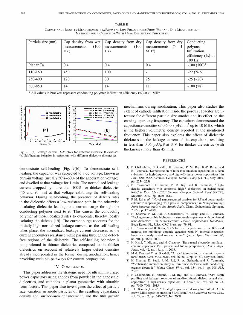
2) Leakage Current Characteristics: The capacitors werecharacterized for leakage properties by growing dielectrics ofdifferent thicknesses, as mentioned in Section II. Fig. 9(a)shows the normalized I–V plot for capacitors (with metal astop electrode) for the dielectric thicknesses of 23, 45, and93 nm for capacitors with an anode particle size of 250–400nm. As expected, the thicker dielectric showed lower leakagecurrent even at higher voltage as compared to thinner dielectricbecause of the relatively lower electric field strength and defectdensity. The thinnest dielectric showed the worst leakagecharacteristics due to leakage contributions from ion hopping,space charge limited conduction, and Schottky mechanismsbased on leakage models [9]. The capacitance measurementafter leakage current measurement showed no change in capac-itance for capacitors with either of the dielectric thicknessesindicating the robustness of the dielectric.
The presence of thicker dielectric reduces the leakagecurrent from ∼2.5 to less than 0.05 μA/μF at 3 V asthe dielectric thickness was increased from 23 to 93 nm.The conducting polymer as cathode was also shown to
1782 IEEE TRANSACTIONS ON COMPONENTS, PACKAGING AND MANUFACTURING TECHNOLOGY, VOL. 6, NO. 12, DECEMBER 2016
TABLE II
CAPACITANCE DENSITY MEASUREMENTS (μF/cm2) AT LOW FREQUENCIES FROM WET AND DRY MEASUREMENT
METHODS FOR A CAPACITOR WITH 45-nm DIELECTRIC THICKNESS
Fig. 9. (a) Leakage current: I–V plots for different dielectric thicknesses.(b) Self-healing behavior in capacitors with different dielectric thicknesses.
demonstrate self-healing [Fig. 9(b)]. To demonstrate self-healing, the capacitor was subjected to a dc voltage, known asburn-in voltage (usually 50%–60% of the anodization voltage),and dwelled at that voltage for 1 min. The normalized leakagecurrent dropped by more than 100% for thicker dielectrics(45 and 93 nm) at that voltage exhibiting the self-healingbehavior. During self-healing, the presence of defects sitesin the dielectric offers a low-resistance path in the otherwiseinsulating dielectric leading to a current surge through theconducting polymer next to it. This causes the conductingpolymer at those localized sites to evaporate, thereby locallyisolating the defects [19]. The current surge accounts for theinitially high normalized leakage current; as the self-healingtakes place, the normalized leakage current decreases as thecurrent encounters resistance while passing through the defect-free regions of the dielectric. The self-healing behavior isnot profound in thinner dielectrics compared to the thickerdielectrics on account of relatively larger defect densitiesalready incorporated in the former during anodization, henceproviding multiple pathways for current propagation.
IV. CONCLUSION
This paper addresses the strategic need for ultraminiaturizedpower capacitors using anodes from powder in the nanoscale,dielectrics, and cathodes in planar geometries with ultrathinform factors. This paper also investigates the effect of particlesize variation in anode particles on the resulting capacitancedensity and surface-area enhancement, and the film growth
mechanisms during anodization. This paper also studies theextent of cathode infiltration inside the porous capacitor archi-tecture for different particle size anodes and its effect on theensuing operating frequency. The capacitors demonstrated thecapacitance densities of 0.6–0.8 μF/mm2 up to 10 MHz, whichis the highest volumetric density reported at the mentionedfrequency. This paper also explores the effect of dielectricthickness on the leakage current of the capacitors, resultingin less than 0.05 μA/μF at 3 V for thicker dielectrics (withthicknesses more than 45 nm).
REFERENCES
[1] P. Chakraborti, S. Gandhi, H. Sharma, P. M. Raj, K.-P. Rataj, andR. Tummala, “Demonstration of ultra-thin tantalum capacitors on siliconsubstrates for high-frequency and high-efficiency power applications,” inProc. 65th IEEE Electron. Compon. Technol. Conf. (ECTC), May 2015,pp. 2254–2258.
[2] P. Chakraborti, H. Sharma, P. M. Raj, and R. Tummala, “High-density capacitors with conformal high-k dielectrics on etched-metalfoils,” in Proc. 62nd IEEE Electron. Compon. Technol. Conf. (ECTC),May/Jun. 2012, pp. 1640–1643.
[3] P. M. Raj et al., “Novel nanostructured passives for RF and power appli-cations: Nanopackaging with passive components,” in Nanopackaging:From Nanomaterials to the Atomic Scale. Cham, Switzerland: Springer,2015, pp. 175–189.
[4] H. Sharma, P. M. Raj, P. Chakraborti, Y. Wang, and R. Tummala,“Package-compatible high-density nano-scale capacitors with conformalnano-dielectrics,” in Nanoelectronic Device Applications Handbook,Boca Raton, FL, USA: CRC Press, pp. 79–91.
[5] H. Chazono and H. Kishi, “DC-electrical degradation of the BT-basedmaterial for multilayer ceramic capacitor with Ni internal electrode:Impedance analysis and microstructure,” Jpn. J. Appl. Phys., vol. 40,no. 9B, p. 5624, 2001.
[6] H. Kishi, Y. Mizuno, and H. Chazono, “Base-metal electrode-multilayerceramic capacitors: Past, present and future perspectives,” Jpn. J. Appl.Phys., vol. 42, no. 1R, p. 1, 2003.
[7] M.-J. Pan and C. A. Randall, “A brief introduction to ceramic capaci-tors,” IEEE Elect. Insul. Mag., vol. 26, no. 3, pp. 44–50, May/Jun. 2010.
[8] H. Sharma, K. Sethi, P. M. Raj, R. A. Gerhardt, and R. Tummala,“Mechanistic interaction study of thin oxide dielectric with conductingorganic electrode,” Mater. Chem. Phys., vol. 134, no. 1, pp. 508–513,2012.
[9] P. Chakraborti, H. Sharma, P. M. Raj, and R. Tummala, “XPS depthprofiling and leakage properties of anodized titania dielectrics and theirapplication in high-density capacitors,” J. Mater. Sci., vol. 50, no. 23,pp. 7600–7609, 2015.
[10] J. H. Klootwijk et al., “Ultrahigh capacitance density for multiple ALD-grown MIM capacitor stacks in 3-D silicon,” IEEE Electron Device Lett.,vol. 29, no. 7, pp. 740–742, Jul. 2008.
CHAKRABORTI et al.: ULTRATHIN, SUBSTRATE-INTEGRATED, AND SELF-HEALING NANOCAPACITORS 1783
[11] F. Roozeboom, R. Elfrink, J. Verhoeven, J. van den Meerakher, andF. Holthuysen, “High-value MOS capacitor arrays in ultradeep trenchesin silicon,” Microelectron. Eng., vol. 53, pp. 581–584, Jun. 2000.
[12] J. D. Prymak, “Improvements with polymer cathodes in aluminum andtantalum capacitors,” in Proc. 16th Annu. IEEE Appl. Power Electron.Conf. Expo. (APEC), Mar. 2001, pp. 1210–1218.
[13] K. R. M. Stenzel, N. Miyashita, R. D. Otterstedt, J. Messe-Marktscheffel,and C. Schnitter, “Paste technology for next generation of ultra-thintantalum capacitors,” in Proc. CARTS Int., Symp. Passive Electron.Compon., Santa Clara, CA, USA, 2014, pp. 75–83.
[14] J. D. Sloppy, Z. Lu, E. C. Dickey, and D. D. Macdonald, “Growthmechanism of anodic tantalum pentoxide formed in phosphoric acid,”Electrochim. Acta, vol. 87, pp. 82–91, Jan. 2013.
[15] M. M. Lohrengel, H. Haas, K. P. Rataj, and C. Schnitter, “Oxide filmson sintered tantalum for electrolytic capacitors,” J. Electrochem. PlatingTechnol., Jul. 2013, doi: 10.12850/ISSN2196-0267.JEPT4750
[16] J. D. Sloppy, “Anodization mechanism and properties of bi-layer tanta-lum oxide formed in phosphoric acid,” Ph.D. dissertation, Dept. Mater.Sci. Eng., Pennsylvania State Univ., State College, PA, USA, 2009.
[17] J. D. Sloppy, D. D. Macdonald, and E. C. Dickey, “Growth lawsof bilayer anodized tantalum oxide films formed in phosphoric acid,”J. Electrochem. Soc., vol. 157, no. 5, pp. C157–C165, 2010.
[18] J. D. Sloppy, N. J. Podraza, E. C. Dickey, and D. D. Macdonald, “Com-plex dielectric functions of anodic bi-layer tantalum oxide,” Electrochim.Acta, vol. 55, no. 28, pp. 8751–8757, 2010.
[19] J. D. Prymak, “Replacing MnO2 with conductive polymer in tantalumcapacitors,” KEMET Electron. Corp., Greenville, SC, USA, 1999.
Parthasarathi Chakraborti received theM.S. degree in polymer and textile engineeringfrom North Carolina State University, Raleigh, NC,USA, in 2010, and the Ph.D. degree in materialscience and engineering from the Georgia Instituteof Technology, Atlanta, GA, USA, in 2016.
He is currently a Post-Doctoral Researcher withnanoEngineered Materials (nGimat), Norcross,GA, USA, where he is involved in developmentof next-generation thin-films for applicationsincluding radio-frequency-based passive elements
and super-oleophobic coatings for spacecraft habitat. He has co-authoredover 15 publications in international peer-reviewed journals and conferences,as well as two book chapters. He has one pending patent. His researchinterests are in the areas of sensors and actuators, thin-film passives, and,semiconductor packaging.
Himani Sharma received the M.S. degree andPh.D. degree in chemistry from the University ofDelhi, New Delhi, India, in 2002 and 2006, respec-tively.
She joined the Georgia Institute of Technology,Atlanta, GA, USA, as a Research Scientist-II. Shewas a Research Associate with the Electrical Engi-neering Department, Alabama A&M University,Huntsville, AL, USA, on an NSA-funded project.She has authored over 45 publications in interna-tional peer-reviewed journals and conferences. She
has co-authored one book and another book chapter and one pending patent.Her current research interests include development of materials for next-generation electronics and packaging.
Dr. Sharma received the Best Poster Award for high density capacitors in the2012 IEEE Electronic Component and Technology Conference.
Markondeya Raj Pulugurtha received theB.S. degree from IIT Kanpur, Kanpur, India,in 1993, the M.S. degree from the Indian Instituteof Science, Bangalore, India, in 1995, and thePh.D. degree in ceramic engineering from RutgersUniversity, New Brunswick, NJ, USA, in 1999.
He is currently a Research Professor and aProgram Manager for the Power and RF FunctionalComponents and Modules Program with the 3-DSystems Packaging Research Center (PRC), GeorgiaInstitute of Technology, Atlanta, GA, USA, where
he provides leadership in power-supply component integration on silicon,glass and organic substrates for power conversion and integrity, RF andprecision components, antennas, diplexers, matching networks, nonlineardevices, integrated rf and power modules, and fine-pitch interconnections.He has co-authored over 250 publications, which includes 11 books, eightpatents with others pending.
Dr. Raj received over 15 best paper awards for his conference and journalpublications which include the Distinguished Scholar Award from theMicrobeam Analysis Society, the IEEE TRANSACTIONS OF ADVANCED
PACKAGING Commendable Paper Award, the IEEE Outstanding TechnicalPaper, the IEEE ECTC Best-Poster Award, and the Philips Best Paper Award.He is also the Co-Chair of the IEEE CPMT Nanopackaging TechnicalCommittee and the USA CPMT Representative of the IEEE NanotechnologyCouncil. He is also the Chair of the High-speed, Wireless & Componentsthrust in the CPMT, the Electronics and Component Technology Conference.
Kamil-Paul Rataj was born in Poland in 1986.He received the doctoral degree in electrochemistryfrom Heinrich-Heine-University Düsseldorf, Düssel-dorf, Germany, in 2013.
He is currently a Project Manager with theResearch and Development Department, H.C. StarckGmbH, Goslar, Germany, where he is involved intantalum and niobium. He is currently involvedin the development of new electronic compo-nents from tantalum and other metals and recy-cling of those, and the development of tanta-
lum paste based capacitors, but also tantalum/niobium and those alloysfor 3-D printing. His current research interests include microelectrochem-istry, passivity, hydrogen permeation, tantalum capacitors and electro-chemical machining, electrochemical transients, impedance spectroscopy,X-ray photoelectron spectroscopy, and atomic force microscopy.
Christopher Schnitter received the Diploma andPh.D. degrees in chemistry from the Georg-August-University of Göttingen, Göttingen, Ger-many, in 1996 and 1998, respectively.
He is with the Georg-August-University of Göt-tingen, where he has been involved in synthesisand characterization of new organoaluminum and-gallium compounds for application in catalysis andMOCVD. In 1998, he joined the Central Research& Development Division of H. C. Starck, Goslar,Germany, as a Research and Development (R&D)
Project and Applied Technology Manager and was involved in differentprojects in tantalum and niobium capacitor powder development. In 2004,he became the Manager of the Capacitor Materials R&D Group with H.C.Starck GmbH, working on tantalum and niobium powders, PEDOT conductivepolymers, and electroceramics, and he became the Head of the new R&DDepartment in 2009, working on the development of different refractorymetal and ceramic powders (e.g., tungsten, non-oxide ceramic powders likecarbides, nitrides, borides, etc.). He is currently also the Director of R&D withH.C. Starck Tantalum and Niobium GmbH, where he is responsible for newproduct development, product, and process designs and yielding improvementsfor Ta and Nb metal powders and compounds of these metals for use in manydifferent applications in electronics, optics, chemicals, aviation, and medical.

1784 IEEE TRANSACTIONS ON COMPONENTS, PACKAGING AND MANUFACTURING TECHNOLOGY, VOL. 6, NO. 12, DECEMBER 2016
Nathan Neuhart was born in The Woodlands,TX, USA, in 1993. He is currently pursuingthe B.Sc. degree in biomedical engineering fromthe Georgia Institute of Technology, Atlanta, GA,USA..
He joined the 3-D Systems Packaging ResearchCenter, Georgia Institute of Technology, in 2015, asa Student Intern.
Shubham Jain is currently pursuing the jointB.Tech. and M.Tech. degree in ceramic engineer-ing from IIT (Banaras Hindu University) Varanasi,Varanasi, India.
He was a Junior Research Fellow with the Materi-als Research Department, Indian Institute of Science,Bangalore, India, from 2015 to 2016. He receivedtwo internships with the Georgia Institute of Tech-nology, Atlanta, GA, USA, in 2013 and 2015,respectively. His current research interests includeadvanced ceramics, ultrahigh temperature ceramics,
bio ceramics, multifunctional composites, materials, nanomaterials, nanocom-posites, nanotechnology, biomaterials, and SOFCs.
Saumya Gandhi was born in India in 1988.He received the B.Tech. degree from Mukesh PatelSchool of Technology Management and Engineer-ing, Mumbai, India, in 2010, and the M.S. andPh.D. degrees from the Georgia Institute of Technol-ogy, Atlanta, GA, USA, in 2012 and 2015, respec-tively.
He joined the 3-D Systems Packaging ResearchCenter, Georgia Institute of Technology, in 2011as a Graduate Research Assistant. He joined TexasInstruments, Dallas, TX, USA, in 2015, as a Pack-
aging Engineer. His current research interests include design, fabrication, andcharacterization of passive components for power module applications.
Rao R. Tummala (M’88–SM’90–F’94–LF’16) iscurrently a Distinguished and an Endowed ChairProfessor in electrical and computer engineering andmaterials science and engineering with the GeorgiaInstitute of Technology, Atlanta, GA, USA. He isalso the Founding Director of the MicrosystemsPackaging Research Center (PRC), Atlanta, pio-neering Moore’s Law for Systems by his System-on-Package vision. The PRC has been one of thelargest and most comprehensive academic micro-systems packaging research, education, and indus-
try collaboration centers involving over 100 students and 25 faculty fromElectronics and Communication Engineering, Mechanical Engineering, Chem-ical Engineering, and Material Science and Engineering departments, and70 global companies from the U.S., Europe, and Asia. He is also an EminentScholar for the State of Georgia. He was a Fellow with IBM Corporation,Armonk, NY, USA, where he invented a number of major technologies forIBM’s products for displaying, printing, magnetic storage, and packaging.He was the Lead Materials Scientist pioneering the industry’s first plasmadisplay in the 1970s, and the Technical Leader for the industry’s first lowtemperature, co-fired ceramic in 1980. He has authored over 500 technicalpapers, holds 90 U.S. patents and inventions, and authored the modernreference book Microelectronics Packaging Handbook (Springer: 1988), thefirst undergraduate textbook in 2001.
Prof. Tummala is a Fellow of the IMAPS and the American Ceramic Society,a member of the National Academy of Engineering, and the President of theIEEE CPMT Society and the IMAPS Society. He has received 30 academic,industry, and professional society awards.