1747-um013-en-p, remote i/o scanner · the remote i/o (rio) scanner, catalog number 1747-sn, is the...
TRANSCRIPT
Remote I/O Scanner1747-SN
User Manual

Important User Information Solid state equipment has operational characteristics differing from those of electromechanical equipment. Safety Guidelines for the Application, Installation and Maintenance of Solid State Controls (Publication SGI-1.1 available from your local Rockwell Automation sales office or online at http://www.ab.com/manuals/gi) describes some important differences between solid state equipment and hard-wired electromechanical devices. Because of this difference, and also because of the wide variety of uses for solid state equipment, all persons responsible for applying this equipment must satisfy themselves that each intended application of this equipment is acceptable.
In no event will Rockwell Automation, Inc. be responsible or liable for indirect or consequential damages resulting from the use or application of this equipment.
The examples and diagrams in this manual are included solely for illustrative purposes. Because of the many variables and requirements associated with any particular installation, Rockwell Automation, Inc. cannot assume responsibility or liability for actual use based on the examples and diagrams.
No patent liability is assumed by Rockwell Automation, Inc. with respect to use of information, circuits, equipment, or software described in this manual.
Reproduction of the contents of this manual, in whole or in part, without written permission of Rockwell Automation, Inc. is prohibited.
Throughout this manual, when necessary we use notes to make you aware of safety considerations.
WARNINGIdentifies information about practices or circumstances that can cause an explosion in a hazardous environment, which may lead to personal injury or death, property damage, or economic loss.
IMPORTANT Identifies information that is critical for successful application and understanding of the product.
ATTENTION Identifies information about practices or circumstances that can lead to personal injury or death, property damage, or economic loss. Attentions help you:
• identify a hazard
• avoid a hazard
• recognize the consequence
SHOCK HAZARD Labels may be located on or inside the equipment (e.g., drive or motor) to alert people that dangerous voltage may be present.
BURN HAZARD Labels may be located on or inside the equipment (e.g., drive or motor) to alert people that surfaces may be dangerous temperatures.
Summary of Changes
The information below summarizes the changes to this manual since the last printing. Updates to the manual include using RSLogix 500 instead of APS software.
To help you find new and updated information in this release of the manual, we have included change bars as shown to the right of this paragraph.
The table below lists the sections that document new features and additional or updated information on existing features.
For this information: See
configuring RIO using G Files page 4-4
using block transfer instruction (BTR and BTW)
page 5-5
removed Chapter 7 application examples can be found in Chapter 4 and Chapter 5
configuring G files using RSLogix 500 page B-9
block transfer examples for earlier processors
Appendix D
1 Publication 1747-UM013B-EN-P - January 2005

Summary of Changes 2
Publication 1747-UM013B-EN-P - January 2005

Table of ContentsImportant User Information . . . . . . . . . . . . . . . . . . . . . . . . 1-2
Table of Contents Chapter 1Overview System Overview . . . . . . . . . . . . . . . . . . . . . . . . . . . . . . . 1-1
Scanner I/O Image Division . . . . . . . . . . . . . . . . . . . . . 1-3How the Scanner Scans Remote I/O . . . . . . . . . . . . . . . . . 1-4
SLC and Scanner Asynchronous Operation . . . . . . . . . . 1-4How the Scanner Interacts with Adapters . . . . . . . . . . . . . . 1-5Scanner I/O Image Concepts . . . . . . . . . . . . . . . . . . . . . . . 1-6
Example Scanner I/O Image. . . . . . . . . . . . . . . . . . . . . 1-7Transferring Data with RIO Discrete and Block Transfers 1-9Physical and Logical RIO Link Specifications . . . . . . . . . 1-9Extended Node Capability . . . . . . . . . . . . . . . . . . . . . . 1-9Complementary I/O . . . . . . . . . . . . . . . . . . . . . . . . . . . 1-10Complementary I/O: Placing Modules with 2-Slot Addressing 1-12Complementary I/O: Placing Modules with 1-Slot Addressing 1-13Complementary I/O: Placing Modules with 1/2-Slot Addressing . . . . . . . . . . . . . . . . . . . . . . . . . . . . . . . . . 1-14Summary for Placing Modules Used In Complementary I/O. 1-15Complementary I/O Application Considerations . . . . . . 1-17Complementary 1771 I/O Module Details . . . . . . . . . . . 1-17
Hardware Features . . . . . . . . . . . . . . . . . . . . . . . . . . . . . . 1-18Baud Rate DIP Switch . . . . . . . . . . . . . . . . . . . . . . . . . 1-18LEDs . . . . . . . . . . . . . . . . . . . . . . . . . . . . . . . . . . . . . . 1-19RIO Link Connector . . . . . . . . . . . . . . . . . . . . . . . . . . . 1-19Compatible Devices . . . . . . . . . . . . . . . . . . . . . . . . . . . 1-19
Chapter 2Quick Start for Experienced Users Required Tools and Equipment . . . . . . . . . . . . . . . . . . . . . 2-1
Procedures . . . . . . . . . . . . . . . . . . . . . . . . . . . . . . . . . . . . 2-2
Chapter 3Installation and Wiring Compliance to European Union Directives . . . . . . . . . . . . . 3-1
EMC Directive . . . . . . . . . . . . . . . . . . . . . . . . . . . . . . . 3-1Baud Rate Selection . . . . . . . . . . . . . . . . . . . . . . . . . . . . . 3-2Scanner Installation . . . . . . . . . . . . . . . . . . . . . . . . . . . . . . 3-2
Insertion . . . . . . . . . . . . . . . . . . . . . . . . . . . . . . . . . . . 3-3Removal . . . . . . . . . . . . . . . . . . . . . . . . . . . . . . . . . . . 3-4
RIO Link Wiring . . . . . . . . . . . . . . . . . . . . . . . . . . . . . . . . 3-5New Installations . . . . . . . . . . . . . . . . . . . . . . . . . . . . . 3-6For Series A Scanner Retrofits . . . . . . . . . . . . . . . . . . . . 3-7
Start Up . . . . . . . . . . . . . . . . . . . . . . . . . . . . . . . . . . . . . . 3-7Scanner Operation . . . . . . . . . . . . . . . . . . . . . . . . . . . . . . 3-8
At Power Up . . . . . . . . . . . . . . . . . . . . . . . . . . . . . . . . 3-8In Run Mode . . . . . . . . . . . . . . . . . . . . . . . . . . . . . . . . 3-8
1 Publication 1747-UM013B-EN-P - January 2005

Table of Contents 2
When Changing From Run Mode . . . . . . . . . . . . . . . . . 3-8Status LEDs. . . . . . . . . . . . . . . . . . . . . . . . . . . . . . . . . . . . 3-9
Chapter 4Scanner Configuration and Programming
Understanding Remote Input and Output Image Files. . . . . 4-1RIO Configuration Using G Files . . . . . . . . . . . . . . . . . . . . 4-4
Rules for Configuring the Scanner. . . . . . . . . . . . . . . . . 4-7Considerations When Configuring Remote I/O . . . . . . . . . . 4-12
G File Considerations. . . . . . . . . . . . . . . . . . . . . . . . . . 4-12Crossing Logical Rack Boundaries . . . . . . . . . . . . . . . . 4-13
Understanding M Files. . . . . . . . . . . . . . . . . . . . . . . . . . . . 4-14M Files Overview. . . . . . . . . . . . . . . . . . . . . . . . . . . . . 4-14M0 Control File Description . . . . . . . . . . . . . . . . . . . . . 4-16M0 File - RIO Device Inhibit Control. . . . . . . . . . . . . . . 4-17M0 File - RIO Device Reset Control. . . . . . . . . . . . . . . . 4-18M0 File - Remote Output Reset Control . . . . . . . . . . . . . 4-19
Device Reset and Remote Output Reset Considerations. . . . 4-21M1 Status File Description . . . . . . . . . . . . . . . . . . . . . . . . . 4-23
General Communication Status - Enable Device Fault Bit. . . 4-23General Communication Status - Communication Attempted Bit. . . . . . . . . . . . . . . . . . . . . . . . . . . . . . . . . . . . . . . . 4-23RIO Baud Rate Status . . . . . . . . . . . . . . . . . . . . . . . . . . 4-24Logical Device Starting Address Status . . . . . . . . . . . . . 4-24Logical Device Image Size Status . . . . . . . . . . . . . . . . . 4-25Active Device Status. . . . . . . . . . . . . . . . . . . . . . . . . . . 4-26Logical Device Fault Status . . . . . . . . . . . . . . . . . . . . . . 4-27RIO Status Example . . . . . . . . . . . . . . . . . . . . . . . . . . . 4-28
RIO Communication Retry Counter (M1:e.16 -47) . . . . . . . . 4-30Understanding Slot Addressing . . . . . . . . . . . . . . . . . . . . . 4-32SLC/Scanner Configuration . . . . . . . . . . . . . . . . . . . . . . . . 4-33
Chapter 5RIO Block Transfer RIO Block Transfer Theory of Operation . . . . . . . . . . . . . . 5-1
What Is RIO Block Transfer? . . . . . . . . . . . . . . . . . . . . 5-1Using Block Transfer Instructions (BTR and BTW) . . . . . . . 5-5
RIO Block Transfer General Functional Overview . . . . . 5-5Parameters for BTR and BTW. . . . . . . . . . . . . . . . . . . . 5-6Control Status Bits . . . . . . . . . . . . . . . . . . . . . . . . . . . . 5-7Instruction Operation . . . . . . . . . . . . . . . . . . . . . . . . . . 5-11Programming Examples . . . . . . . . . . . . . . . . . . . . . . . . 5-12Comparison to the PLC-5 BTR and BTW . . . . . . . . . . . . 5-16
Chapter 6Troubleshooting Troubleshooting . . . . . . . . . . . . . . . . . . . . . . . . . . . . . . . . 6-1
Publication 1747-UM013B-EN-P - January 2005
Table of Contents 3
Error Codes . . . . . . . . . . . . . . . . . . . . . . . . . . . . . . . . . . . 6-2Retry Counters . . . . . . . . . . . . . . . . . . . . . . . . . . . . . . . . . 6-2Block Transfers . . . . . . . . . . . . . . . . . . . . . . . . . . . . . . . . . 6-2
Appendix ASpecifications Scanner Operating Specifications . . . . . . . . . . . . . . . . . . . . A-1
Network Specifications . . . . . . . . . . . . . . . . . . . . . . . . . . . A-1Throughput Introduction . . . . . . . . . . . . . . . . . . . . . . . . . . A-2
RIO Network Throughput Components. . . . . . . . . . . . . A-2Calculating Throughput . . . . . . . . . . . . . . . . . . . . . . . . . . . A-3
Discrete I/O Throughput without Block Transfers (Tdm-nbt) Present . . . . . . . . . . . . . . . . . . . . . . . . . . . . . . . . . . . . A-3Discrete I/O Throughput with Block Transfers (Tdm-bt) Present . . . . . . . . . . . . . . . . . . . . . . . . . . . . . . . . . . . . A-6Block Transfer Throughput . . . . . . . . . . . . . . . . . . . . A-10RIO Scanner Output Delay Time (TSNo) Tables . . . . . A-13
Appendix BM0 - M1 Files and G Files M0 - M1 Files . . . . . . . . . . . . . . . . . . . . . . . . . . . . . . . . . . B-1
Addressing M0-M1 Files . . . . . . . . . . . . . . . . . . . . . . . . B-2Restrictions on Using M0-M1 Data File Addresses . . . . . B-2Monitoring Bit Addresses . . . . . . . . . . . . . . . . . . . . . . . B-2Transferring Data Between Processor Files and M0 or M1 Files B-4Access Time . . . . . . . . . . . . . . . . . . . . . . . . . . . . . . . . B-4Minimizing the Scan Time . . . . . . . . . . . . . . . . . . . . . . B-7Capturing M0-M1 File Data. . . . . . . . . . . . . . . . . . . . . . B-8Specialty I/O Modules with Retentive Memory . . . . . . . B-8
G Files . . . . . . . . . . . . . . . . . . . . . . . . . . . . . . . . . . . . . . . B-9Configuring G Files using RSLogix 500 . . . . . . . . . . . . . B-9After all devices have been properly mapped, click OK and the G file is automatically configured. This procedure eliminates the bit by bit process needed to configure the G file with other programming tools. . . . . . . . . . . . . . . . B-13Editing G File Data . . . . . . . . . . . . . . . . . . . . . . . . . . B-14
Appendix CRIO Configuration Worksheet Directions . . . . . . . . . . . . . . . . . . . . . . . . . . . . . . . . . . . . . C-1
Appendix DBlock Transfer Examples for Earlier Processors
BTR and BTW Control Logic Examples . . . . . . . . . . . . . . . D-1Block Transfer Read Control Logic Example . . . . . . . . . D-1Block Transfer Write Control Logic Example . . . . . . . . D-4Directional Continuous Block Transfer Example . . . . . . D-6Directional Repeating Block Transfer Example . . . . . . . D-9
Publication 1747-UM013B-EN-P - January 2005
Table of Contents 4
Directional Non-Continuous Block Transfer Example . D-12Bidirectional Continuous Block Transfer Example . . . . D-16Bidirectional Alternating Block Transfer . . . . . . . . . . . D-21Bidirectional Alternating Repeating Block Transfer . . . D-27
GlossaryIndex Rockwell Automation Support . . . . . . . . . . . . . . . . . . . . . . 1-7
Installation Assistance . . . . . . . . . . . . . . . . . . . . . . . . . 1-7New Product Satisfaction Return . . . . . . . . . . . . . . . . . . 1-7
Publication 1747-UM013B-EN-P - January 2005

Chapter 1
Overview
This chapter contains the following information:
• system overview
• how the scanner interacts with the SLC processor
• how the scanner interacts with adapter modules
• scanner I/O image concepts
• extended node capability
• complementary I/O
• scanner features
• compatible network devices
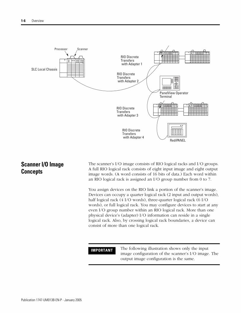
System Overview The Remote I/O (RIO) Scanner, Catalog Number 1747-SN, is the remote I/O scanner for the SLC 500. It enables communication between an SLC processor (SLC 5/02 or later) and remotely located (3,048 meters [10,000 feet] maximum) 1746 I/O chassis and other RIO compatible Allen-Bradley operator interface and control devices. The 1747-SN Scanner communicates with remotely located devices using the Allen-Bradley Remote I/O link. The RIO link consists of a single master (scanner) and multiple slaves (adapters). Communication between devices occurs over twisted pair cable with the devices daisy-chained together. The scanner can reside in any slot of the local SLC chassis except for slot 0.
The Remote I/O (RIO) Scanner, Catalog Number 1747-SN, is the remote I/O scanner for the SLC 500. It enables communication between an SLC processor (SLC 5/02 or later) and remotely located (3,048 meters [10,000 feet] maximum) 1746 I/O chassis and other RIO compatible Allen-Bradley operator interface and control devices. The 1747-SN Scanner communicates with remotely located devices using the Allen-Bradley Remote I/O link. The RIO link consists of a single master (scanner) and multiple slaves (adapters). Communication between devices occurs over twisted pair cable with the devices daisy-chained together. The scanner can reside in any slot of the local SLC chassis except for slot 0.
1 Publication 1747-UM013B-EN-P - January 2005

1-2 Overview
The scanner can be configured for and transfer a maximum of 4 logical racks of discrete data on the RIO link. The scanner provides discrete I/O and block (Series B or later) transfers. Configurations allowed are any combination of quarter, half, three-quarter, or full logical rack devices.
The SLC processor transfers the scanner’s 4 logical racks (32 input image and 32 output image words) of discrete remote I/O image data into the SLC input and output image files. You can adjust the size of the scanner input and output image file during configuration of your SLC system so that the scanner only transfers the discrete I/O data
The scanner transfers input andoutput data between itself and allconfigured network devices overtwisted pair cable. Note that theend-to-end length of the cable can bea maximum of 3,048 meters (10,000feet).
Dataliner Message Display (Adapter/Slave)
PanelView Operator Terminal (Adapter/Slave)
SLC 5/02or LaterProcessor
Remote Chassis
Remote Expansion Chassis
1747-ASB Module(Adapter/Slave)
RediPANEL (Adapter/Slave)
Local SLC Chassis
RIO Scanner(Master of theRIO Link)
The scanner transfers discrete input and output databetween itself, remote adapters, and the SLC processor..Remote adapters consist of 1746 chassis and otherAllen-Bradley operator interface and control devices.
RIOScanner
SLC 5/02or LaterProcessor
Quarter LogicalRackDevice
HalfLogical RackDevice
Three-QuarterLogical RackDevice
Full Logical RackDevice
Half LogicalRackDevice
Full Logical RackDevice
Adapter 1 Adapter 2 Adapter 3 Adapter 4 Adapter 5 Adapter 6
Publication 1747-UM013B-EN-P - January 2005

Overview 1-3
your application program requires. Configuration is done through the confiGuration file (G file). Refer to Chapter 4, Configuration and Programming, for more information.
Scanner I/O Image Division
The scanner allows each adapter to use a fixed amount (user defined) of the scanner’s input and output image. Part of the SLC processor’s image is used by local I/O, the other portion is used by the scanner for remote I/O.
The scanner remote I/O image is divided into logical racks and further divided into logical groups. A full logical rack consists of eight input and eight output image words. A logical group consists of one input and one output word in a logical rack. Each logical group is assigned a number from 0 to 7.
IMPORTANT The SLC 500 processor (SLC 5/02 or later) supports multiple scanners in its local I/O chassis. The maximum number is dependent on the following:
• backplane power requirements (power supply dependent)
• SLC 500 processor I/O data table limit (4,096 I/O)
• processor memory to support the application (SLC 500 processor dependent)
Processor I/O Image Scanner I/O Image AdapterImage
Logical Group 7
Local I/O
Remote I/O(Scanner Image)
Logical Rack 2
Logical Rack 1
Logical Rack 0
Logical Group 0
Publication 1747-UM013B-EN-P - January 2005
1-4 Overview
The scanner image contains the image of each adapter on the RIO link. The adapter is assigned a portion of the scanner image, which is referred to as the adapter image.
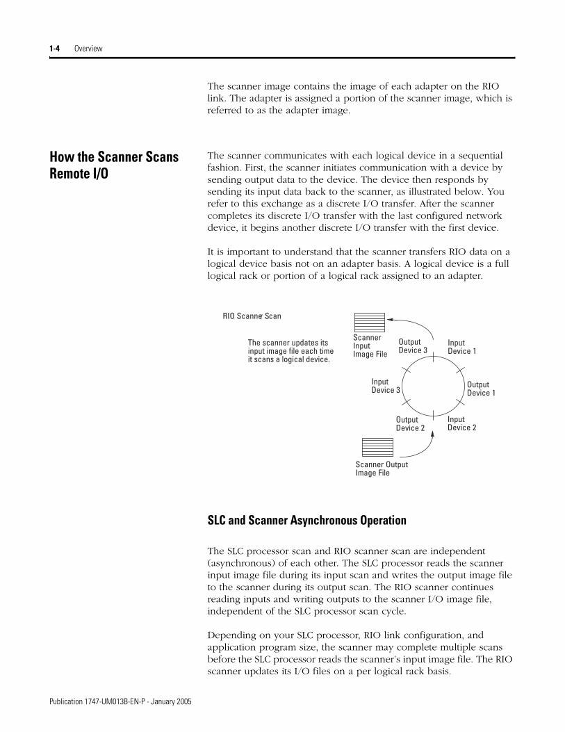
How the Scanner Scans Remote I/O
The scanner communicates with each logical device in a sequential fashion. First, the scanner initiates communication with a device by sending output data to the device. The device then responds by sending its input data back to the scanner, as illustrated below. You refer to this exchange as a discrete I/O transfer. After the scanner completes its discrete I/O transfer with the last configured network device, it begins another discrete I/O transfer with the first device.
It is important to understand that the scanner transfers RIO data on a logical device basis not on an adapter basis. A logical device is a full logical rack or portion of a logical rack assigned to an adapter.
SLC and Scanner Asynchronous Operation
The SLC processor scan and RIO scanner scan are independent (asynchronous) of each other. The SLC processor reads the scanner input image file during its input scan and writes the output image file to the scanner during its output scan. The RIO scanner continues reading inputs and writing outputs to the scanner I/O image file, independent of the SLC processor scan cycle.
Depending on your SLC processor, RIO link configuration, and application program size, the scanner may complete multiple scans before the SLC processor reads the scanner’s input image file. The RIO scanner updates its I/O files on a per logical rack basis.
RIO Scanner Scan
Scanner OutputImage File
The scanner updates itsinput image file each timeit scans a logical device.
OutputDevice 3
OutputDevice 2
OutputDevice 1
InputDevice 3
InputDevice 2
InputDevice 1
ScannerInputImage File
Publication 1747-UM013B-EN-P - January 2005

Overview 1-5
The figure below illustrates the asynchronous operation of the SLC processor and RIO scanner.
How the Scanner Interacts with Adapters
The scanner’s function is to continuously scan the adapters on the RIO link in a consecutive manner. This scan consists of one or more RIO discrete transfers to each adapter on the RIO link.
RIO discrete transfers consist of the scanner sending output image data and communication commands to the adapter that instruct the adapter on how to control its output. (These include run, adapter reset, and reset decide commands.) The adapter responds by sending input data to the scanner. The scanner performs as many RIO discrete transfers as necessary to update the entire adapter image. If RIO discrete transfers do not occur, data is not exchanged between the scanner and adapter. RIO discrete transfers are asynchronous to the processor scan.
SLC Processor
SLC Processor Scan Cycle RIO Scanner Scan Cycle
Program
The scanner updates itsinput image file each timeit scans a logical device.The scanner may scan allof its configured logicaldevices several timesbefore the SLC processorreads the scanner's inputimage file.
The SLC processor reads thescanner input image file into theSLC input image file, processesit, and creates an SLC outputimage file. The SLC processortransfers its output file to thescanner..
SLC InputImage File
SLC OutputImage File
ScannerInputImage File
Scanner OutputImage File
OutputImageDevice 3
OutputImageDevice 2
OutputImageDevice 1
InputImageDevice 3
InputImageDevice 2
InputImageDevice 1
Important: The outputs of the RIO are updated after the end of the first SLC processor scan.
Publication 1747-UM013B-EN-P - January 2005
1-6 Overview
Scanner I/O Image Concepts
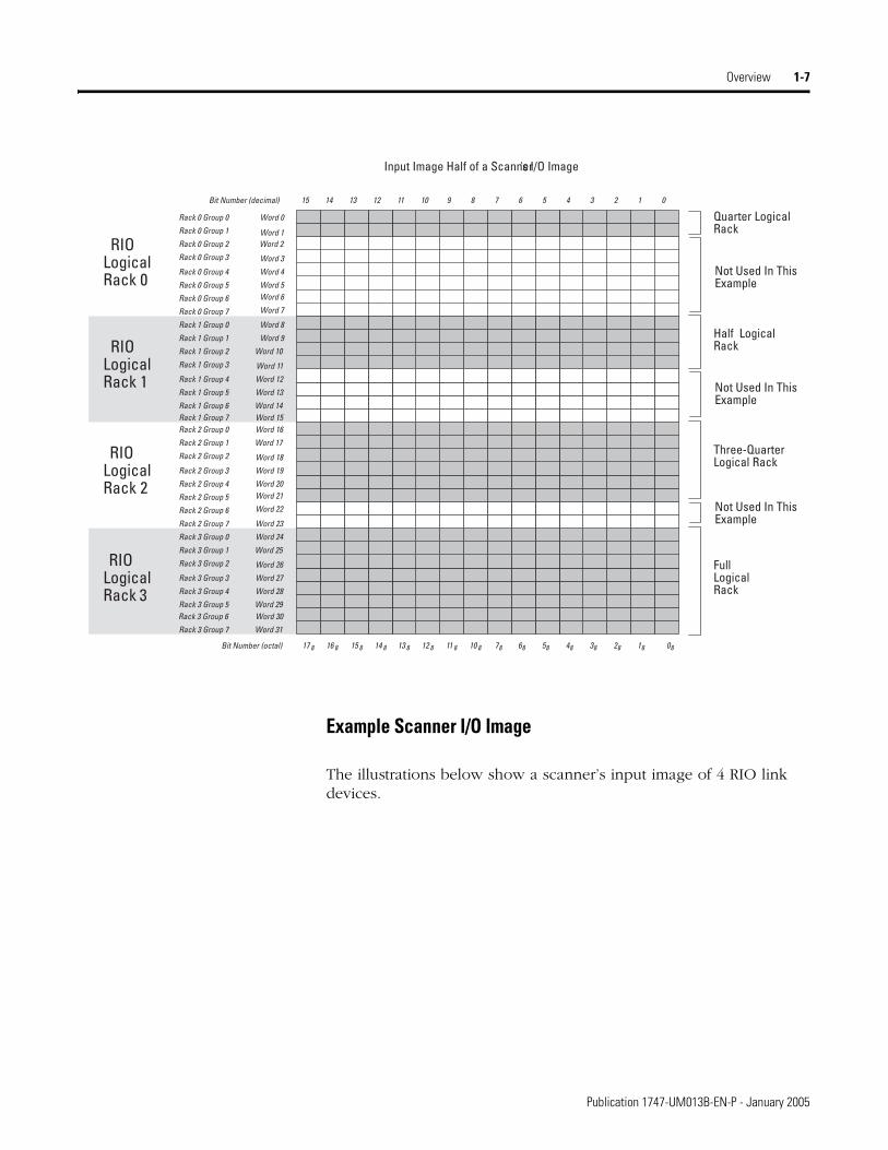
The scanner’s I/O image consists of RIO logical racks and I/O groups. A full RIO logical rack consists of eight input image and eight output image words. (A word consists of 16 bits of data.) Each word within an RIO logical rack is assigned an I/O group number from 0 to 7.
You assign devices on the RIO link a portion of the scanner’s image. Devices can occupy a quarter logical rack (2 input and output words), half logical rack (4 I/O words), three-quarter logical rack (6 I/O words), or full logical rack. You may configure devices to start at any even I/O group number within an RIO logical rack. More than one physical device’s (adapter) I/O information can reside in a single logical rack. Also, by crossing logical rack boundaries, a device can consist of more than one logical rack.
RediPANEL
PanelView OperatorTerminal
SLC Local Chassis
ScannerProcessor
RIO DiscreteTransfers with Adapter 1
RIO DiscreteTransfers with Adapter 2
RIO DiscreteTransfers with Adapter 3
RIO DiscreteTransfers with Adapter 4
IMPORTANT The following illustration shows only the input image configuration of the scanner’s I/O image. The output image configuration is the same.
Publication 1747-UM013B-EN-P - January 2005
Overview 1-7
Example Scanner I/O Image
The illustrations below show a scanner’s input image of 4 RIO link devices.
Rack 3 Group 6
Rack 3 Group 7
Rack 1 Group 2
Rack 1 Group 3
Rack 1 Group 0
Rack 1 Group 1
Rack 1 Group 6
Rack 1 Group 4
Rack 1 Group 5
Rack 0 Group 6
Rack 0 Group 7
Rack 0 Group 4
Rack 0 Group 5
Rack 0 Group 2
Rack 0 Group 3
0123456789101112131415Bit Number (decimal)
Word 0
Word 1Word 2
Word 3
Word 4
Word 7
Word 8
Word 9
Word 10
Word 11
Word 12
Word 13
Word 14
Word 5Word 6
Word 30
Word 31
Rack 0 Group 0
Rack 0 Group 1
Rack 3 Group 1
Rack 3 Group 2
Rack 2 Group 7
Rack 3 Group 0
Rack 3 Group 5
Rack 3 Group 3
Rack 3 Group 4
Rack 2 Group 5
Rack 2 Group 6
Rack 2 Group 3
Rack 2 Group 4
Rack 2 Group 1
Rack 2 Group 2
Word 15Word 16
Word 17
Word 18
Word 19
Word 22
Word 23
Word 24
Word 25
Word 26
Word 27
Word 28
Word 29
Word 20Word 21
Rack 1 Group 7Rack 2 Group 0
RIOLogicalRack 0
081828384858687810 811 812 813 814 815 816 817 8Bit Number (octal)
RIOLogicalRack 1
RIOLogicalRack 2
RIOLogicalRack 3
Quarter LogicalRack
Half LogicalRack
Three-QuarterLogical Rack
FullLogicalRack
Input Image Half of a Scanner's I/O Image
Not Used In ThisExample
Not Used In ThisExample
Not Used In ThisExample
Publication 1747-UM013B-EN-P - January 2005

1-8 Overview
RIOScanner
SLC 5/02or LaterProcessor
Three-Quarter LogicalRack DeviceBegins at LogicalRack 1, Group 0.
Half Logical RackDeviceBegins at LogicalRack 2, Group 0.
Quarter Logical RackDeviceBegins at LogicalRack 2, Group 4.
Full Logical RackDeviceBegins at LogicalRack 0, Group 0.
Device 1 Device 2 Device 3 Device 4
Rack 3 Group 6
Rack 3 Group 7
Rack 1 Group 2
Rack 1 Group 3
Rack 1 Group 0
Rack 1 Group 1
Rack 1 Group 6
Rack 1 Group 4
Rack 1 Group 5
Rack 0 Group 6
Rack 0 Group 7
Rack 0 Group 4
Rack 0 Group 5
Rack 0 Group 2
Rack 0 Group 3
0123456789101112131415Bit NumberInput FileAddress
I:e.0I:e.1I:e.2I:e.3I:e.4I:e.5I:e.6I:e.7I:e.8I:e.9I:e.10I:e.11I:e.12I:e.13I:e.14
I:e.30I:e.31
Word 0
Word 1
Word 2
Word 3
Word 4
Word 7
Word 8
Word 9
Word 10
Word 11
Word 12
Word 13
Word 14
Word 5Word 6
Word 30
Word 31
Rack 0 Group 0
Rack 0 Group 1
Rack 3 Group 1
Rack 3 Group 2
Rack 2 Group 7
Rack 3 Group 0
Rack 3 Group 5
Rack 3 Group 3
Rack 3 Group 4
Rack 2 Group 5
Rack 2 Group 6
Rack 2 Group 3
Rack 2 Group 4
Rack 2 Group 1
Rack 2 Group 2
I:e.15I:e.16I:e.17I:e.18I:e.19I:e.20I:e.21I:e.22I:e.23I:e.24I:e.25I:e.26I:e.27I:e.28I:e.29
Word 15Word 16
Word 17
Word 18
Word 19
Word 22
Word 23
Word 24
Word 25
Word 26
Word 27
Word 28
Word 29
Word 20Word 21
Rack 1 Group 7Rack 2 Group 0
RIOLogicalRack 0
Device 1
Device 2
Device 3
Device 4
e = slot number of the SLC chassis containing the scanner
081828384858687810 811 812 813 814 815 816 817 8Bit Number (octal)
RIOLogicalRack 1
RIOLogicalRack 2
RIOLogicalRack 3
Important: The illustration below shows only the scanner's input image. The output image looks the same.
Not Used
Not Used
Publication 1747-UM013B-EN-P - January 2005
Overview 1-9
Transferring Data with RIO Discrete and Block Transfers
Input and output image data and command information are quickly exchanged between a scanner and adapter using RIO discrete transfers. RIO discrete transfers are the simplest and fastest way a scanner and adapter communicate with each other. RIO discrete transfers, which are transparent to the user, consist of the scanner sending the output image data to the adapter, and the adapter transmitting input data to the scanner. Each RIO discrete transfer also contains scanner commands for the adapter.
Through your control program, you command the SLC processor to initiate RIO block transfers, which directs the scanner to exchange large amounts of data to/from an adapter. Block Transfers (BTs) use the basic RIO discrete transfer mechanism of the RIO link. However, the actual transfer of data occurs asynchronous to the discrete transfers. It is possible for several discrete transfers to occur before the scanner processes a block transfer. Refer to Chapter 5, RIO Block Transfer for more details.
Physical and Logical RIO Link Specifications
The maximum number of adapters with which your scanner can communicate is determined by the scanner’s and adapter’s physical and logical specifications, as described below:
• Physical Specifications are the maximum number of adapters that can be connected to the scanner. For more information, see Extended Node Capability below.
• Logical Specifications for the scanner are the maximum number of logical racks the scanner can address, how the logical racks can be assigned, and whether the scanner can perform BTs.
Extended Node Capability
Extended node functionality allows you to connect up to 32 physical devices on an RIO link. You must use 82 Ohm RIO link resistors in an extended node configuration. You can only use extended node if all RIO link devices have extended node capability. (Refer to the Compatible Devices table at the end of this chapter, or to the specifications of your device.) The 1747-SN Series B Scanner has extended node capability. However, the smallest logical rack division is 1/4 logical rack and the scanner image size is 4 logical racks. Therefore, the scanner is limited to 16 devices unless complementary
Publication 1747-UM013B-EN-P - January 2005

1-10 Overview
I/O is used. Refer to the following section for more information on complementary I/O.
Complementary I/O
Complementary I/O is very useful when portions of your input and output images are unused because it allows the images of two adapters to overlap each other in the scanner’s I/O image. To use complementary I/O, the I/O image from one adapter must be the mirror (complement) of the other. This means that there must be an input module in the primary chassis and an output module in the same slot of the complementary chassis. This enables total use of the scanner’s 32 input and 32 output word image for I/O addressing of up to 1024 discrete points.
If you want to use complementary I/O, two adapters that support this function are required (e.g., 1747-ASB modules). One adapter is configured (via its DIP switches) as a primary chassis, the other as a complementary chassis. If a primary chassis exists, it is scanned first.
Primary and complementary chassis cannot have the same logical rack number. The logical rack numbers must be assigned to the primary and complementary racks as shown below:
ATTENTION Because the primary and complementary chassis images overlap, input and specialty combination I/O modules must never share the same image location. Inputs received by the scanner may be incorrect and RIO block transfers will not be serviced properly. If an output module shares its output image with another output module, both output modules receive the same output information.
Primary Chassis Logical Rack Number
Complementary Chassis Logical Rack Number
Decimal Octal
0 8 10
1 9 11
2 10 12
3 11 13
Publication 1747-UM013B-EN-P - January 2005
Overview 1-11
Guidelines for Configuring Complementary I/O
When you configure your remote system for complementary I/O, follow these guidelines:
• You can place an output module in the primary chassis opposite another output module in the complementary chassis; they use the same bits in the output image table. However, we do not recommend this placement of modules for redundant I/O.
• You cannot use complementary I/O with a chassis that uses 32-point I/O modules and 1-slot addressing or 16-point I/O modules with 2-slot addressing.
• Do not place an input module in the primary chassis opposite an input module in the complementary chassis; they will use the same bits in the input image table.
ATTENTION If the logical rack numbers are not properly assigned, unpredictable operation of both ASB modules results. No ASB module errors occur. Refer to your ASB module user manual for specific information on setting the address of the complementary chassis. (For example, in the 1771-ASB manual the addresses for the complementary chassis are referred to as complementary chassis 0-3.)
Publication 1747-UM013B-EN-P - January 2005

1-12 Overview
Complementary I/O: Placing Modules with 2-Slot Addressing
The following figures illustrate a possible module placement to configure complementary I/O using 2-slot addressing.
I 8
O 8
I 16
BTI 8O 8
I 8
O 8
O 16
O 8
O 8
O 8
BT
O 8
EMPTY
O 8
O 8
O 8
I 8
I 8
EMPTY
EMPTY
1 2
O 8
2
EMPTY
2
EMPTY
2
0 1 2 3 4 5
I 16
I 16
I 16
O 16
O 16
O 16
0 1 2 3 4 5
I 16
I 16
I 16
O 16
O 16
O 16
Outputs in the complementary chassis would use the same bits in the output image table as the outputs in the primary chassis. You cannotplace inputs in the complementary chassis.
Example 1
Example 2
1 = Output modules use the same output image table bits. This is not recommended.2 = Must be empty if corresponding primary slot is a block transfer module.
Important: With 2-slot addressing, if an input module resides in either slot associated with alogical group of the primary chassis, an input module cannot reside in that logical group' scomplementary chassis.
1 1
1
Publication 1747-UM013B-EN-P - January 2005

Overview 1-13
Complementary I/O: Placing Modules with 1-Slot Addressing
The figure below illustrates a possible module placement to configure complementary I/O using 1-slot addressing.
I 16
EMPTY
1
2
0 1 2 3 4 5
Example 1
Example 2
I = Input Module (8- or 16-point) O = Output Module (8- or 16-point)BT = Block Transfer Module1 = Output modules use the same output image table bits. This is not recommended.
I 16
I 16
I 16
O 16
O 16
O16
O 16
BT I 16
O 16
O 16
6 7 0 1 2 3
O 16
O 16
I 16
I 16
I 16
O 16
O 16
1
I 16
O 16
I 16
O 16
I 16
0 1 2 3 4 5
I 16
I 16
6 7 0 1 2 3
O 16
O 16
I 16
I 16
I 16
I 16
I 16
I 16
I 16
I 16
I 16
O 16
O 16
O 16
O 16
O 16
O 16
O 16
O 16
O 16
O 16
2 = Must be empty if corresponding primary slot is block transfer..
Publication 1747-UM013B-EN-P - January 2005

1-14 Overview
Complementary I/O: Placing Modules with 1/2-Slot Addressing
The figure below illustrates a possible module placement to configure complementary I/O using 1-slot addressing.
I
1
2
01 23 45 67 01 23
Example 1
Example 2
I = Input Module (8-, 16-, or 32-point) O = Output Module (8-, 16-, or 32-point)BT = Block Transfer Module1 = Output modules use the same output image table bits. This is not recommended.
I I OO O O BT I
45 67 01 23
O O I I IO O
1
I
I I
O O
I I I I I I I I
O O O O O O O O
2 = Must be empty if corresponding primary slot is block transfer.
01 23 45 67 01 23 45 67 01 23
O
O
EMPTY
Publication 1747-UM013B-EN-P - January 2005

Overview 1-15
Summary for Placing Modules Used In Complementary I/O
Discrete Modules
Block Transfer Modules
The following example illustrates how I/O modules requiring two words of the input or output image can leave unused image space.
Addressing Method Types of Modules used Placement
2-slot 8-point Install input modules opposite output modules, and output modules opposite input modules.(1)
(1) If an input module resides in either slot associated with a logical group of the primary chassis, an input module cannot reside in that logical group’s complementary chassis.
1-slot 8-point, 16-point
1/2-slot 8-point, 16-point, 32-point
Addressing Method Placement
2-slot The right slot of the primary I/O group can be another block transfer module, or an 8-point input or output module.
The left slot of the complementary I/O group must be empty.
In the right slot of the complementary I/O group, you can place an 8-point output module; this slot must be empty if the corresponding slot in the primary I/O group is a block transfer module.
1-slot Leave the corresponding I/O group in the complementary chassis empty.
1/2-slot Leave the corresponding I/O group in the complementary chassis empty.
Publication 1747-UM013B-EN-P - January 2005

1-16 Overview
0 1 2 3 4 5 6 7 8
Slot Pair 1 2 3 4
I I I IO O O O
0 1 2 3 4 5 6 7 8
Slot Pair 1 2 3 4
O O O O
OI = Input Module
= Output Module
Input Image Output Image
= unused image space
Slot 1
Slot 2
Slot 3
Slot 4
Slot 5
Slot 6
Slot 7
Slot 8
Slot 1
Slot 2
Slot 3
Slot 4
Slot 5
Slot 6
Slot 7
Slot 8
1
Slot Pair
2
3
4
Slot 1
Slot 2
Slot 3
Slot 4
Slot 5
Slot 6
Slot 7
Slot 8
Slot 1
Slot 2
Slot 3
Slot 4
Slot 5
Slot 6
Slot 7
Slot 8
1
2
3
4
Input Imagefrom Primary Chassis
Output Imagefrom Primary Chassis
Output Imagefrom Complementary Chassis
Slot 1
Slot 2
Slot 3
Slot 4
Slot 5
Slot 6
Slot 8
Slot 1
Slot 2
Slot 3
Slot 4
Slot 5
Slot 6
Slot 8
Slot 1
Slot 2
Slot 3
Slot 4
Slot 5
Slot 6
Slot 7
Slot 8
Slot 1
Slot 2
Slot 3
Slot 4
Slot 5
Slot 6
Slot 7
Slot 8
Slot 7Slot 7
Input Imagefrom Complementary Chassis
Slot Slot
Primary Chassis Complementary Chassis
Slot 1
Slot 2
Slot 3
Slot 4
Slot 5
Slot 6
Slot 7
Slot 8
Slot 1
Slot 2
Slot 3
Slot 4
Slot 5
Slot 6
Slot 7
Slot 8
1
2
3
4
Slot 1
Slot 2
Slot 3
Slot 4
Slot 5
Slot 6
Slot 7
Slot 8
Slot 1
Slot 2
Slot 3
Slot 4
Slot 5
Slot 6
Slot 7
Slot 8
1
2
3
4
Slot 1
Slot 2
Slot 3
Slot 4
Slot 5
Slot 6
Slot 8
Slot 1
Slot 2
Slot 3
Slot 4
Slot 5
Slot 6
Slot 8
Slot 1
Slot 2
Slot 3
Slot 4
Slot 5
Slot 6
Slot 7
Slot 8
Slot 1
Slot 2
Slot 3
Slot 4
Slot 5
Slot 6
Slot 7
Slot 8
Slot 7Slot 7
Primary Chassis I/O Image Complementary Chassis I/O Image
Scanner's I/O Image
1
2
3
4
Slot 1
Slot 2
Slot 3
Slot 4
Slot 5
Slot 6
Slot 8
Slot 1
Slot 2
Slot 3
Slot 4
Slot 5
Slot 6
Slot 8
Slot 1
Slot 2
Slot 3
Slot 4
Slot 5
Slot 6
Slot 7
Slot 8
Slot 1
Slot 2
Slot 3
Slot 4
Slot 5
Slot 6
Slot 7
Slot 8
Slot 7Slot 7
Slot 1
Slot 2
Slot 3
Slot 4
Slot 5
Slot 6
Slot 7
Slot 8
Slot 1
Slot 2
Slot 3
Slot 4
Slot 5
Slot 6
Slot 7
Slot 8
1
2
3
4
Slot 1
Slot 2
Slot 3
Slot 4
Slot 5
Slot 6
Slot 7
Slot 8
Slot 1
Slot 2
Slot 3
Slot 4
Slot 5
Slot 6
Slot 7
Slot 8
Group 0
Group 2
Group 4
Group 6
Group 1
Group 3
Group 5
Group 7Group 0
Group 2
Group 4
Group 6
Group 1
Group 3
Group 5
Group 7
Both images are overlapped in thescanner. The overlapped image
appears where the primary chassisimage is configured to reside.
In this case, the primary chassisimage is configured as starting
logical rack 0 and starting logicalgroup 0.
I I I I
Primary Chassis Configured As:Logical Rack Number 0
Logical Group Number 0Image Size (logical groups) 16
Addressing Mode 1/2-slotPrimary/Complementary Primary
Complementary Chassis Configured As: Logical Rack Number 8 (decimal)
Logical Group Number 0Image Size (logical groups) 16
Addressing Mode 1/2-slotPrimary/Complementary Complementary
LogicalRack 0
LogicalRack 1
078157 01017
DecimalOctal
078157 01017
DecimalOctal
078157 01017
DecimalOctal
078157 01017
DecimalOctal
078157 01017
DecimalOctal
078157 01017
DecimalOctal
Slot Pair Slot Pair Slot Pair
Slot Pair Slot Pair
Publication 1747-UM013B-EN-P - January 2005

Overview 1-17
Complementary I/O Application Considerations
If you configure a complementary device to use more I/O image space than an associated primary device, then block transfers can only be performed to locations in the complementary device that have associated I/O image space in the primary device. For example, if a primary device is 1/2 logical rack and a complementary device is a full logical rack, block transfers can be performed only in the first 1/2 logical rack of the complementary device. Attempting block transfers in the last half of the complementary device will result in a BT error (error - 11 - device not configured).
Complementary 1771 I/O Module Details
Use the following modules in either primary or complementary I/O chassis opposite any type of module:
• Communication Adapter Module (1771-KA2)
• Communication Controller Module (1771-KE)
• PLC-2 Family/RS-232-C Interface Module (1771-KG)
• Fiber Optics Converter Module (1771-AF)
• DH/DH+ Communication Adapter Module (1785-KA)
• DH+/RS-232C Communications Interface Module (1785-KE)
Use the following modules in either primary or complementary I/O chassis opposite any type of module. However, these modules do not work as stand-alone modules; each one has an associated master module. Use care when placing the master modules in the I/O chassis:
• Analog Input Expander Module (1771-E1, -E2, -E3)
• Analog Output Expander Module (1771-E4)
• Servo (Encoder Feedback) Expander Module (1771-ES)
• Pulse Output Expander Module (1771-OJ)
Word 7
Word 5Word 6
Word 3
Word 1Word 2
Word 0
Word 4LogicalRack 8
Word 7
Word 5Word 6
Word 3Word 4
Word 1Word 2
Word 0
LogicalRack 0
1/2 logical rack configured and usable
1/2 logical rack not configured
1/2 logical rack configured and usa
1/2 logical rack configured, but notusable for BT sinceWords 4-7 are not configured for the primary device.
1/2 logical rackconfigured and usable
1/2 logical rack configured, but not usable for BT since Words 4 to 7 are not configured for the primary device.
Publication 1747-UM013B-EN-P - January 2005
1-18 Overview
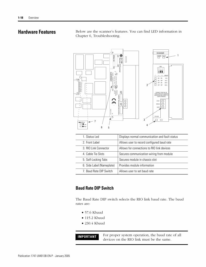
Hardware Features Below are the scanner’s features. You can find LED information in Chapter 6, Troubleshooting.
Baud Rate DIP Switch
The Baud Rate DIP switch selects the RIO link baud rate. The baud rates are:
• 57.6 Kbaud
• 115.2 Kbaud
• 230.4 Kbaud
SCANNER
12
N O
SLC 500
CAT
SERIAL NO.
Remote I/O Scanner
SERFAC)
ULLISTED IN
D. CONT. EQ.
FOR HAZ. LOC. A196
CLASS I, GROUPS A, B, C AND D, DIV.2 OPERATIN
G )
SATEM
PERATURECODE T3C
B
HOSTFRN
.:FRN
.:PLUG
CURRENT REQUIREM
ENT: 600 m
A @5VDC
MAKE IN
U.S.A.
1 2NO
COMM FAULT
SW1
CONNECT ONE END OFCABLE SHIELD TO CHASSISMOUNTING BOLT. REFER T O
USER'S MANUAL.
1747±SN
LINE 1
LINE 2
SHIELD
1 2 KBAUD
ON
OFF
OFF OFF
OFF
ON
ON
ON
57.6
115.2
230.4
230.4
/
2
1
3
456
7
1. Status Led Displays normal communication and fault status
2. Front Label Allows user to record configured baud rate
3. RIO Link Connector Allows for connections to RIO link devices
4. Cable Tie Slots Secures communication wiring from module
5. Self-Locking Tabs Secures module in chassis slot
6. Side Label (Nameplate) Provides module information
7. Baud Rate DIP Switch Allows user to set baud rate
IMPORTANT For proper system operation, the baud rate of all devices on the RIO link must be the same.
Publication 1747-UM013B-EN-P - January 2005

Overview 1-19
LEDs
Two LEDs allow you to monitor scanner and communication status.
FAULT LED - allows you to monitor scanner status. This LED is red. The FAULT LED’s normal state is off; therefore, it is off whenever the scanner is operating properly.
COMM LED - allows you to monitor communication with all configured devices. This LED is green and its normal state is on once the processor has entered Run mode. The LED is red if there is a communication problem. The COMM LED status information is valid only when the FAULT LED is off.
RIO Link Connector
This 3-pin male connector connects the scanner to the RIO link. The Allen-Bradley repair part number is 1746-RT29.
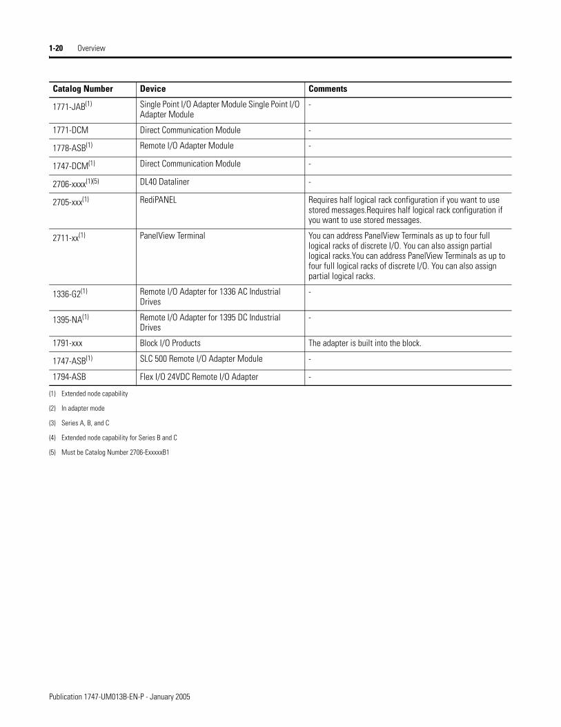
Compatible Devices
Catalog Number Device Comments
1785-LT/x(1) (2) PLC- 5/15 (in adapter mode) -
1785-LT2(1)(2) PLC- 5/25 (in adapter mode) -
1785-LT3(1)(2) PLC- 5/12 (in adapter mode) -
1785-L30x(1)(2) PLC- 5/30 (in adapter mode) -
1785-L40x(1)(2) PLC- 5/40 (in adapter mode) -
1785-L60x(1)(2) PLC- 5/60 (in adapter mode) -
1771-ASC Remote I/O Adapter Module -
1771-ASB(3) (4) Remote I/O Adapter Module -
1771-AM1(1) 1-Slot I/O Chassis W/Integral Power Supply and Adapter
-
1771-AM2(1) 2-Slot I/O Chassis W/Integral Power Supply and Adapter
-
1784-F30D(1) Plant Floor Terminal Remote I/O Expansion Module
-
1771-RIO Remote I/O Interface Module -
Publication 1747-UM013B-EN-P - January 2005
1-20 Overview
1771-JAB(1) Single Point I/O Adapter Module Single Point I/O Adapter Module
-
1771-DCM Direct Communication Module -
1778-ASB(1) Remote I/O Adapter Module -
1747-DCM(1) Direct Communication Module -
2706-xxxx(1)(5) DL40 Dataliner -
2705-xxx(1) RediPANEL Requires half logical rack configuration if you want to use stored messages.Requires half logical rack configuration if you want to use stored messages.
2711-xx(1) PanelView Terminal You can address PanelView Terminals as up to four full logical racks of discrete I/O. You can also assign partial logical racks.You can address PanelView Terminals as up to four full logical racks of discrete I/O. You can also assign partial logical racks.
1336-G2(1) Remote I/O Adapter for 1336 AC Industrial Drives
-
1395-NA(1) Remote I/O Adapter for 1395 DC Industrial Drives
-
1791-xxx Block I/O Products The adapter is built into the block.
1747-ASB(1) SLC 500 Remote I/O Adapter Module -
1794-ASB Flex I/O 24VDC Remote I/O Adapter -
(1) Extended node capability
(2) In adapter mode
(3) Series A, B, and C
(4) Extended node capability for Series B and C
(5) Must be Catalog Number 2706-ExxxxxB1
Catalog Number Device Comments
Publication 1747-UM013B-EN-P - January 2005
Chapter 2
Quick Start for Experienced Users
This chapter helps you to get started using the RIO Scanner. We base the procedures here on the assumption that you have a basic understanding of SLC 500 products.
You must:
• understand electronic process control
• be able to interpret the ladder logic instructions for generating the electronic signals that control your application
Because it is a start-up guide for experienced users, this chapter does not contain detailed explanations about the procedures listed. It does, however, reference other chapters in this book where you can get more detailed information. It also references other documentation that may be helpful if you are unfamiliar with programming techniques or system installation requirements.
If you have any questions, or are unfamiliar with the terms used or concepts presented in the procedural steps, always read the referenced chapters and other recommended documentation before trying to apply the information.
This chapter:
• tells you what tools and equipment you need
• lists preliminary considerations
• describes when to address, configure and program the module
• explains how to install and wire the module
• discusses system power-up procedures
Required Tools and Equipment
Have the following tools and equipment ready:
• medium blade screwdriver
• programming equipment
• termination kit (package of resistors and ring lug included with the scanner)
• approximately 15 inches of #20 AWG for grounding the drain shield to the SLC chassis (for Series A retrofits)
• an adequate length of RIO communication cable (Belden 9463) for your specific application
1 Publication 1747-UM013B-EN-P - January 2005
2-2 Quick Start for Experienced Users
Procedures 1. Check the contents of the shipping box.
Unpack the module making sure that the contents include:
• RIO Scanner (Catalog Number 1747 SN)
• termination kit
If the contents are incomplete, call your local Allen-Bradley representative for assistance.
2. Ensure you chassis supports placement of the 1747-SN module.
Review the power requirements of your system to see that your chassis supports placement of the scanner module. The scanner consumes 600 mA @ 5VDC.
For modular style systems, calculate the total load on the system power supply using the procedure described in the SLC 500 Modular Hardware Style User Manual, Publication 1747-UM011.
See Chapter 3, Installation and Wiring and Appendix A Specifications in this manual.
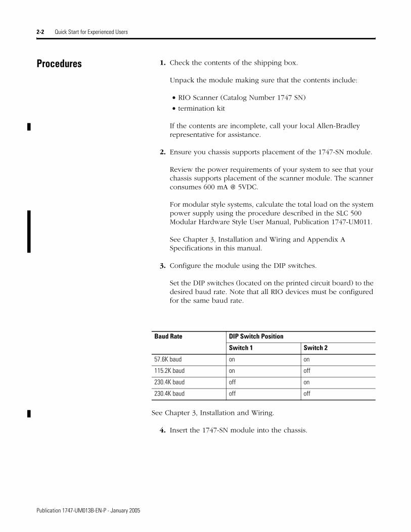
3. Configure the module using the DIP switches.
Set the DIP switches (located on the printed circuit board) to the desired baud rate. Note that all RIO devices must be configured for the same baud rate.
See Chapter 3, Installation and Wiring.
4. Insert the 1747-SN module into the chassis.
Baud Rate DIP Switch Position
Switch 1 Switch 2
57.6K baud on on
115.2K baud on off
230.4K baud off on
230.4K baud off off
Publication 1747-UM013B-EN-P - January 2005

Quick Start for Experienced Users 2-3
Make sure system power is off; then insert the scanner module into your 1746 chassis. In this example procedure, local slot 1 is selected.
See Chapter 3, Installation and Wiring.
5. Connect all RIO link devices.
Ensure that you:
• Daisy chain each RIO link device.
• Ground the shield drain wire to the nearest chassis mounting bolt.
• Connect the appropriate termination resistors on each end of the link.
6. Configure the system.
Set up your system I/O configuration for the particular slot in which you installed the scanner (slot 1 in this example). If your module is not listed in your software version, select Other and enter the scanner input module ID code (13608) at the prompt on the I/O configuration display.
See Chapter 4, Configuration and Programming.
ATTENTION Never install, remove, or wire modules with power applied to the chassis or devices wired to the module.
Make sure system power is off; then insert the scanner module into your 1746 chassis. In this example procedure, local slot 1 is selected.
CardGuide
Top and BottomModule Release(s)
Publication 1747-UM013B-EN-P - January 2005

2-4 Quick Start for Experienced Users
7. Enter the number of scanned words.
Enter the number of Scanned Input and Output Words using the Specialty I/O and Advanced Setup menus. The default value is 32 I/O words. You can specify less than 32 and reduce the processor scan time by transferring only the part of the input and output image that your application requires. It is important that you do not set either of these values to 0. If you do, the scanner will not work correctly.
See Chapter 4, Configuration and Programming.
8. Set the M0 - M1 and G file sizes.
Using the Specialty I/O Configuration menu, set the M1 and M0 file sizes to 32 words (48 words if using complementary I/O). (32 words is the minimum required for operation.) If you do not set the M1 and M0 file sizes to at least 32 words, the programming device will not allow you to access the M files in the SLC control program.
Set the G file size to 3 (5 if using complementary I/O) using the Specialty I/O Configuration menu. Do the programming necessary to configure the M0 and M1 Block Transfer Buffers. If you are using the block transfer (BT) function, you should set the M1 and M0 file sizes to 3,300. Ensure that you refer to chapter 5 before completing this selection.
Write the remainder of the SLC control program that specifies how your scanner will transfer data to/from the SLC processor and RIO devices.
Refer to Chapter 4, Configuration and Programming and Chapter 5, RIO Block Transfer.
9. Go through the system start-up procedure.
a. Apply power.
b. Download your program to the SLC.
c. Place the SLC in Run mode.
The scanner’s FAULT LED is off and the COMM LED is green, as shown below. (This is the valid LED pattern when in Run mode or after a Run mode to Program mode transition.)
See Chapter 3, Installation and Wiring.
Publication 1747-UM013B-EN-P - January 2005

Quick Start for Experienced Users 2-5
FAULT LED is off.COMM LED is green.
SCANNERFAULTCOMM
Publication 1747-UM013B-EN-P - January 2005

2-6 Quick Start for Experienced Users
Publication 1747-UM013B-EN-P - January 2005
Chapter 3
Installation and Wiring
This chapter contains the information necessary to:
• select the baud rate
• insert the scanner into the SLC chassis
• wire the RIO link
• power up the scanner
Compliance to European Union Directives
If this product has the CE mark, it is approved for installation within the European Union and EEA regions. It has been designed and tested to meet the following directives.
EMC Directive
This product is tested to meet Council Directive 89/336/EEC Electromagnetic Compatibility (EMC) and the following standards, in whole or in part, documented in a technical construction file:
• EN 50081-2EMC - Generic Emission Standard, Part 2 - Industrial Environment
• EN 50082-2EMC - Generic Immunity Standard, Part 2 - Industrial Environment
This product is intended for use in an industrial environment.
1 Publication 1747-UM013B-EN-P - January 2005

3-2 Installation and Wiring
Baud Rate Selection Below are supported baud rates and switch positions:
The figure below shows the location of the DIP switches on the scanner. Also, the DIP switch settings are shown for each baud rate.
Scanner Installation Installation procedures for this module are the same as for any other discrete I/O or specialty module. Refer to the illustration on page 2-4 to identify chassis and module components listed in the procedures below.
Baud Rate DIP Switch Position
Switch 1 Switch 2
57.6K baud on on
115.2K baud on off
230.4K baud off on
230.4K baud off off
IMPORTANT For proper RIO link system operation, all devices must be configured for the same baud rate.
Baud RateDIP Switch
57.6K baud 115.2K baud
230.4K baud 230.4K baud
12
N O
12
N O
12
N O
12
N O
Publication 1747-UM013B-EN-P - January 2005
Installation and Wiring 3-3
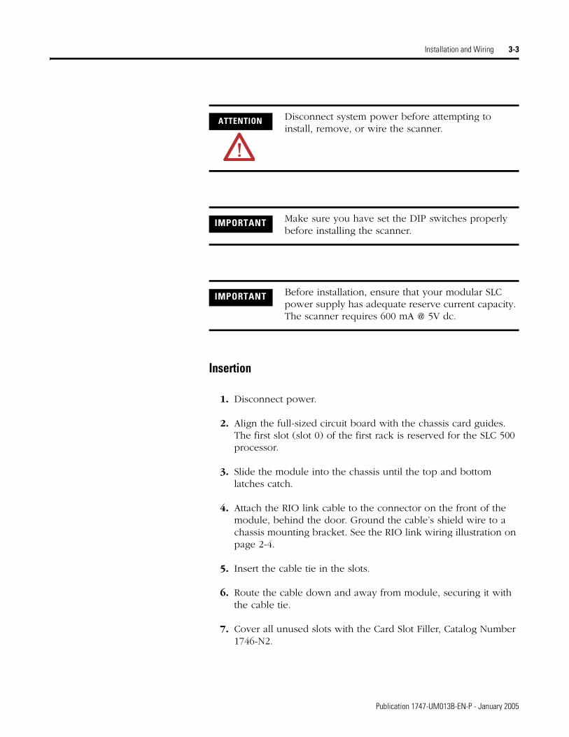
Insertion
1. Disconnect power.
2. Align the full-sized circuit board with the chassis card guides. The first slot (slot 0) of the first rack is reserved for the SLC 500 processor.
3. Slide the module into the chassis until the top and bottom latches catch.
4. Attach the RIO link cable to the connector on the front of the module, behind the door. Ground the cable’s shield wire to a chassis mounting bracket. See the RIO link wiring illustration on page 2-4.
5. Insert the cable tie in the slots.
6. Route the cable down and away from module, securing it with the cable tie.
7. Cover all unused slots with the Card Slot Filler, Catalog Number 1746-N2.
ATTENTION Disconnect system power before attempting to install, remove, or wire the scanner.
IMPORTANT Make sure you have set the DIP switches properly before installing the scanner.
IMPORTANT Before installation, ensure that your modular SLC power supply has adequate reserve current capacity. The scanner requires 600 mA @ 5V dc.
Publication 1747-UM013B-EN-P - January 2005
3-4 Installation and Wiring
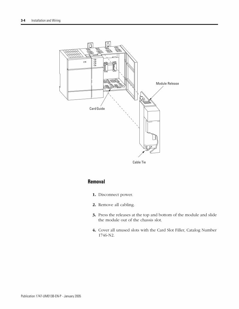
Removal
1. Disconnect power.
2. Remove all cabling.
3. Press the releases at the top and bottom of the module and slide the module out of the chassis slot.
4. Cover all unused slots with the Card Slot Filler, Catalog Number 1746-N2.
Card Guide
Module Release
Cable Tie
Publication 1747-UM013B-EN-P - January 2005

Installation and Wiring 3-5
RIO Link Wiring The scanner is connected to other devices on the RIO link in a daisy chain (serial) configuration. There are no restrictions governing the space between each device, provided the maximum cable distance (Belden 9463) is not exceeded.
A 1/2 watt terminating resistor (included with the module) must be attached across line 1 and line 2 of the connectors at each end (scanner and last physical device) of the RIO link. The value of the resistor depends on the baud rate and extended node capability, as shown in the table that follows.
IMPORTANT To use extended node, all devices on the RIO link must support it. Refer to each device’s user manual.
Baud Rate Maximum Cable Distance (Belden 9463)
Resistor Size
Using Extended Node Capability
57.6K baud 3048 meters (10,000 feet) 82 ohm 1/2 Watt Brown - Green - Brown - Gold115.2K baud 1524 meters (5000 feet)
230.4K baud 762 meters (2500 feet)
Not Using Extended Node Capability
57.6K baud 3048 meters (10,000 feet) 150 ohm 1/2 Watt Brown - Green - Brown - Gold115.2K baud 1524 meters (5000 feet)
230.4K baud 762 meters (2500 feet) 82 ohm 1/2 Watt Gray - Red - Black - Gold
Publication 1747-UM013B-EN-P - January 2005

3-6 Installation and Wiring
New Installations
To ensure a proper earth ground of the cable shield, follow these steps:
1. While the RIO link connector is plugged into the scanner and lines 1 and 2 are connected, strip the cable back to expose enough shield drain wire to reach a chassis mounting bracket.
2. Attach the ring terminal lug (supplied) to the end of the shield drain wire.
3. Attach the ring terminal lug to the SLC chassis mounting bracket. Note that for new installations the middle (shield) terminal is not used when connecting to the scanner.
LINE 1 _______
LINE 2 _______
RIO LinkConnector
RIO Scanner
Line 1 ± Blue
Line 2 ± Clear
Chassis MountingBracket
RIO LinkConnector
TerminatingResistor Last PhysicalDevice End
TerminatingResistorScanner End
Shield Drain Wire
Shield ± Shield
SHIELD _____
For New InstallationsUsing Series BScanners
For Series AScannerRetrofits
Shield Drain Wire
Ring Lug
Publication 1747-UM013B-EN-P - January 2005

Installation and Wiring 3-7
For Series A Scanner Retrofits
To eliminate the need to strip the cable back, follow these steps:
1. Attach the shield wire and a short piece of #20 AWG wire (dotted line) to the shield lug of the RIO Link Connector.
2. Attach the other end of the #20 AWG wire to the ring terminal lug.
3. Attach the ring terminal lug to a chassis mounting bracket.
Start Up The following steps will assist you in the start up of your RIO system.
1. Apply power to your SLC processor. If you powered down with the SLC processor in Program, Test, or Fault mode, you will have to place your processor in Run mode.
When power is applied to your scanner it requires about three seconds to complete its power up diagnostics. During this time, the FAULT and COMM LEDs cycle on and off. After the diagnostics are complete and the SLC processor is in the Run mode, the scanner’s LEDs are in the following states:
• The FAULT LED is off.
• The COMM LED is green.
IMPORTANT The RIO cable shield must be grounded at the scanner end only.
IMPORTANT The RIO cable shield must be grounded at the scanner end only. Ensure that the unshielded portion of the link communication wire (blue and clear) is as short as possible.
IMPORTANT The above states are true only if the scanner is configured properly and all RIO link devices are communicating.
Publication 1747-UM013B-EN-P - January 2005
3-8 Installation and Wiring
2. Make sure you have configured your SLC processor and downloaded an application program. (Refer to chapter 4.)
3. Make sure power is applied to all devices on the RIO link.
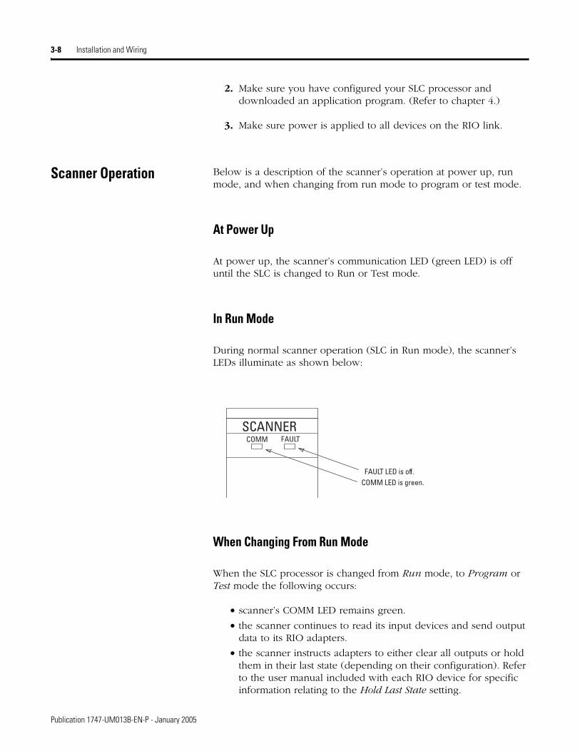
Scanner Operation Below is a description of the scanner’s operation at power up, run mode, and when changing from run mode to program or test mode.
At Power Up
At power up, the scanner’s communication LED (green LED) is off until the SLC is changed to Run or Test mode.
In Run Mode
During normal scanner operation (SLC in Run mode), the scanner’s LEDs illuminate as shown below:
When Changing From Run Mode
When the SLC processor is changed from Run mode, to Program or Test mode the following occurs:
• scanner’s COMM LED remains green.
• the scanner continues to read its input devices and send output data to its RIO adapters.
• the scanner instructs adapters to either clear all outputs or hold them in their last state (depending on their configuration). Refer to the user manual included with each RIO device for specific information relating to the Hold Last State setting.
FAULT LED is off.COMM LED is green.
SCANNERFAULTCOMM
Publication 1747-UM013B-EN-P - January 2005

Installation and Wiring 3-9
Status LEDs The scanner has two LEDs that indicate its operating status, FAULT and COMM. The FAULT LED indicates the scanner’s overall status. The COMM LED indicates the RIO link communication status.
The FAULT LED is off whenever the scanner is configured and operating properly. The COMM LED state is valid only when the FAULT LED is off.
The table below provides the scanner and communication status as indicated by the FAULT and COMM LEDs.
IMPORTANT If you are using Block Transfer (BT) functionality, BTs may not function on adapters in Hold Last State settings. Refer to each device’s user manual for information on BTs and Hold Last State settings.
FAULT LED COMM LED Status Information
Flashing Red Not Applicable Scanner configuration error
No RIO link communication attempted
Duplicate scanner detected on RIO link
Red Not Applicable Major fault on scanner
No RIO link communication attempted
Off Red Hardware fault detected
Off Off Scanner is operating properly
Scanner is offline (no RIO link communication attempted)
Off Green Scanner is operating properly
Scanner is online (active communication established with all devices)
Off Flashing Green Scanner is operation properly
At least one configured RIO link device is not communicating
Off Flashing Red Scanner is operating properly
None of the configured RIO link devices are communicating
Publication 1747-UM013B-EN-P - January 2005

3-10 Installation and Wiring
Publication 1747-UM013B-EN-P - January 2005
Chapter 4
Scanner Configuration and Programming
This chapter contains information necessary to:
• understand remote I/O image files
• understand RIO configuration using G files
• control and view RIO devices using the M0 and M1 files
• understand slot addressing
• quickly configure the RIO Scanner
Understanding Remote Input and Output Image Files
The SLC system allows you to assign up to 32 words of input and output image data to a scanner. This allows your scanner to access a maximum of 4 full logical racks (512 input and output points) of data from remote devices.
1 Publication 1747-UM013B-EN-P - January 2005

4-2 Scanner Configuration and Programming
The illustration below shows how logical racks, logical groups, and words are allocated within the I/O image files. Note that this illustration describes the input image file. The scanner’s output image file is the same, except that its addressing scheme starts with O:e.0 and ends with 0:e.31.
078150717 10Bit Number Octal
LogicalRack 1
LogicalRack 0
LogicalRack 2
LogicalRack 3
Input ImageOutput Image
SN Series B Scanner(RIO Master)
Scanner Input and Output Images
The scanner accommodates up to 32 words of output forremote devices.
The scanner accommodates up to 32 words of input from remote devices.
Word 10Word 1 1
Word 8Word 9
Word 14
Word 12Word 13
Word 15
LogicalRack 1
Word 7
Word 5Word 6
Word 3Word 4
Word 1Word 2
Word 0
LogicalRack 0
LogicalRack 2
Word 26Word 27
Word 24Word 25
Word 30
Word 28Word 29
Word 31
Word 23
Word 21Word 22
Word 19Word 20
Word 17Word 18
Word 16
LogicalRack 3
Bit Number Decimal 078150717 10Bit Number Octal
Bit Number Decimal
Word 10Word 1 1
Word 8Word 9
Word 14
Word 12Word 13
Word 15
Word 7
Word 5Word 6
Word 3Word 4
Word 1Word 2
Word 0
Word 26Word 27
Word 24Word 25
Word 30
Word 28Word 29
Word 31
Word 23
Word 21Word 22
Word 19Word 20
Word 17Word 18
Word 16
Note that some RIO devices (e.g.,1771) use octal bit numbers.
Publication 1747-UM013B-EN-P - January 2005
Scanner Configuration and Programming 4-3
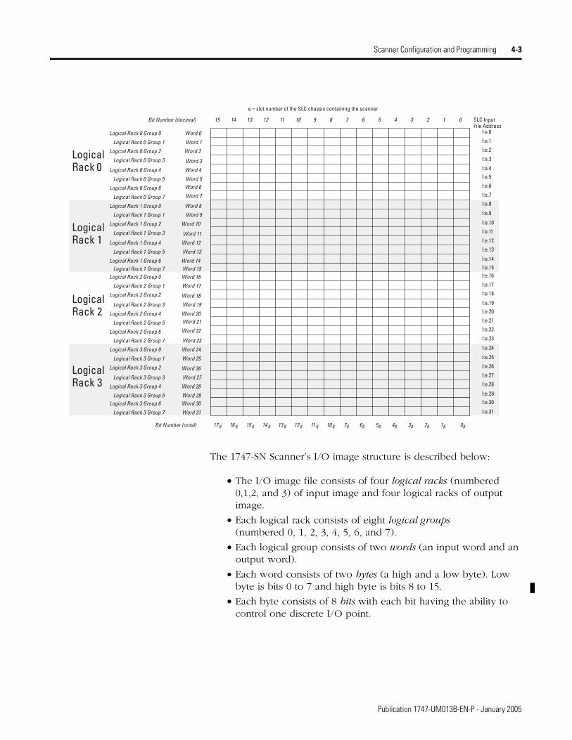
The 1747-SN Scanner’s I/O image structure is described below:
• The I/O image file consists of four logical racks (numbered 0,1,2, and 3) of input image and four logical racks of output image.
• Each logical rack consists of eight logical groups (numbered 0, 1, 2, 3, 4, 5, 6, and 7).
• Each logical group consists of two words (an input word and an output word).
• Each word consists of two bytes (a high and a low byte). Low byte is bits 0 to 7 and high byte is bits 8 to 15.
• Each byte consists of 8 bits with each bit having the ability to control one discrete I/O point.
Logical Rack 3 Group 6
Logical Rack 3 Group 7
Logical Rack 1 Group 2
Logical Rack 1 Group 3
Logical Rack 1 Group 0
Logical Rack 1 Group 1
Logical Rack 1 Group 6
Logical Rack 1 Group 4
Logical Rack 1 Group 5
Logical Rack 0 Group 6
Logical Rack 0 Group 7
Logical Rack 0 Group 4
Logical Rack 0 Group 5
Logical Rack 0 Group 2
Logical Rack 0 Group 3
0123456789101112131415Bit Number (decimal) SLC InputFile Address
I:e.0
I:e.1
I:e.2
I:e.3
I:e.4I:e.5
I:e.6
I:e.7
I:e.8
I:e.9
I:e.10
I:e.11
I:e.12
I:e.13
I:e.14
I:e.30
I:e.31
Word 0
Word 1
Word 2
Word 3
Word 4
Word 7
Word 8
Word 9
Word 10
Word 11
Word 12
Word 13
Word 14
Word 5Word 6
Word 30
Word 31
Logical Rack 0 Group 0
Logical Rack 0 Group 1
Logical Rack 3 Group 1
Logical Rack 3 Group 2
Logical Rack 2 Group 7
Logical Rack 3 Group 0
Logical Rack 3 Group 5
Logical Rack 3 Group 3
Logical Rack 3 Group 4
Logical Rack 2 Group 5
Logical Rack 2 Group 6
Logical Rack 2 Group 3
Logical Rack 2 Group 4
Logical Rack 2 Group 1
Logical Rack 2 Group 2
I:e.15I:e.16
I:e.17
I:e.18
I:e.19I:e.20
I:e.21
I:e.22
I:e.23
I:e.24
I:e.25
I:e.26
I:e.27
I:e.28
I:e.29
Word 15Word 16
Word 17
Word 18
Word 19
Word 22
Word 23
Word 2 4
Word 25
Word 26
Word 27
Word 28
Word 29
Word 20Word 21
Logical Rack 1 Group 7Logical Rack 2 Group 0
LogicalRack 0
LogicalRack 1
LogicalRack 2
LogicalRack 3
081828384858687810 811 812 813 814 815 816 817 8Bit Number (octal)
e = slot number of the SLC chassis containing the scanner
Publication 1747-UM013B-EN-P - January 2005
4-4 Scanner Configuration and Programming
RIO Configuration Using G Files
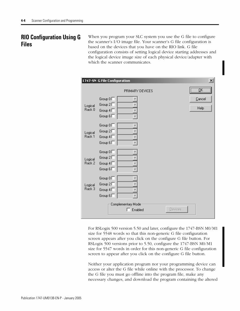
When you program your SLC system you use the G file to configure the scanner’s I/O image file. Your scanner’s G file configuration is based on the devices that you have on the RIO link. G file configuration consists of setting logical device starting addresses and the logical device image size of each physical device/adapter with which the scanner communicates.
For RSLogix 500 version 5.50 and later, configure the 1747-BSN M0/M1 size for 5548 words so that this non-generic G file configuration screen appears after you click on the configure G file button. For RSLogix 500 versions prior to 5.50, configure the 1747-BSN M0/M1 size for 5547 words in order for this non-generic G file configuration screen to appear after you click on the configure G file button.
Neither your application program nor your programming device can access or alter the G file while online with the processor. To change the G file you must go offline into the program file, make any necessary changes, and download the program containing the altered
Publication 1747-UM013B-EN-P - January 2005
Scanner Configuration and Programming 4-5
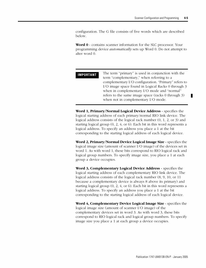
configuration. The G file consists of five words which are described below.
Word 0 - contains scanner information for the SLC processor. Your programming device automatically sets up Word 0. Do not attempt to alter word 0.
Word 1, Primary/Normal Logical Device Address - specifies the logical starting address of each primary/normal RIO link device. The logical address consists of the logical rack number (0, 1, 2, or 3) and starting logical group (0, 2, 4, or 6). Each bit in this word represents a logical address. To specify an address you place a 1 at the bit corresponding to the starting logical address of each logical device.
Word 2, Primary/Normal Device Logical Image Size - specifies the logical image size (amount of scanner I/O image) of the devices set in word 1. As with word 1, these bits correspond to RIO logical rack and logical group numbers. To specify image size, you place a 1 at each group a device occupies.
Word 3, Complementary Logical Device Address - specifies the logical starting address of each complementary RIO link device. The logical address consists of the logical rack number (8, 9, 10, or 11 because a complementary device is always 8 above its primary) and starting logical group (0, 2, 4, or 6). Each bit in this word represents a logical address. To specify an address you place a 1 at the bit corresponding to the starting logical address of each logical device.
Word 4, Complementary Device Logical Image Size - specifies the logical image size (amount of scanner I/O image) of the complementary devices set in word 3. As with word 3, these bits correspond to RIO logical rack and logical group numbers. To specify image size you place a 1 at each group a device occupies.
IMPORTANT The term “primary” is used in conjunction with the term “complementary,” when referring to a complementary I/O configuration. “Primary” refers to I/O image space found in Logical Racks 0 through 3 when in complementary I/O mode and “normal” refers to the same image space (racks 0 through 3) when not in complementary I/O mode.
Publication 1747-UM013B-EN-P - January 2005
4-6 Scanner Configuration and Programming
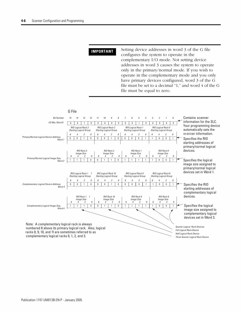
IMPORTANT Setting device addresses in word 3 of the G file configures the system to operate in the complementary I/O mode. Not setting device addresses in word 3 causes the system to operate only in the primary/normal mode. If you wish to operate in the complementary mode and you only have primary devices configured, word 3 of the G file must be set to a decimal “1,” and word 4 of the G file must be equal to zero.
1
0
1
0123456789101112131415
0000010000000100
10000001000100
100111111100111
Bit Number
024602460246
RIO Logical Rack 3Starting Logical Group
0246
I/O Mix, Word 0
Primary/Normal Logical Device Address,Word 1
Primary/Normal Logical Image Size,Word 2
G File
Contains scannerinformation for the SLC.Your programming deviceautomatically sets thescanner information.Specifies the RIOstarting addresses ofprimary/normal logicaldevices.
Specifies the logicalimage size assigned toprimary/normal logicaldevices set in Word 1.
RIO Rack 0 Image Size
0246
RIO Rack 1Image Size
0246
RIO Rack 2Image Size
0246
RIO Rack 3Image Size
0246
Full Logical Rack DeviceHalf Logical Rack DeviceThree Quarter Logical Rack Device
Quarter Logical Rack Devices
RIO Logical Rack 2Starting Logical Group
RIO Logical Rack 1Starting Logical Group
RIO Logical Rack 0Starting Logical Group
1 100100001000100
1001111101100111
024602460246
RIO Logical Rack 1 1Starting Logical Group
0246
Complementary Logical Device Address,Word 3
Complementary Logical Image Size,Word 4
RIO Rack 8 Image Size
0246
RIO Rack 9Image Size
0246
RIO Rack 10Image Size
0246
RIO Rack 1 1Image Size
0246
RIO Logical Rack 10Starting Logical Group
RIO Logical Rack 9Starting Logical Group
RIO Logical Rack 8Starting Logical Group
Specifies the RIOstarting addresses ofcomplementary logicaldevices.
Specifies the logicalimage size assigned tocomplementary logicaldevices set in Word 3.
Note: A complementary logical rack is alwaysnumbered 8 above its primary logical rack. Also, logicalracks 8, 9, 10, and 11 are sometimes referred to ascomplementary logical racks 0, 1, 2, and 3.
Publication 1747-UM013B-EN-P - January 2005
Scanner Configuration and Programming 4-7
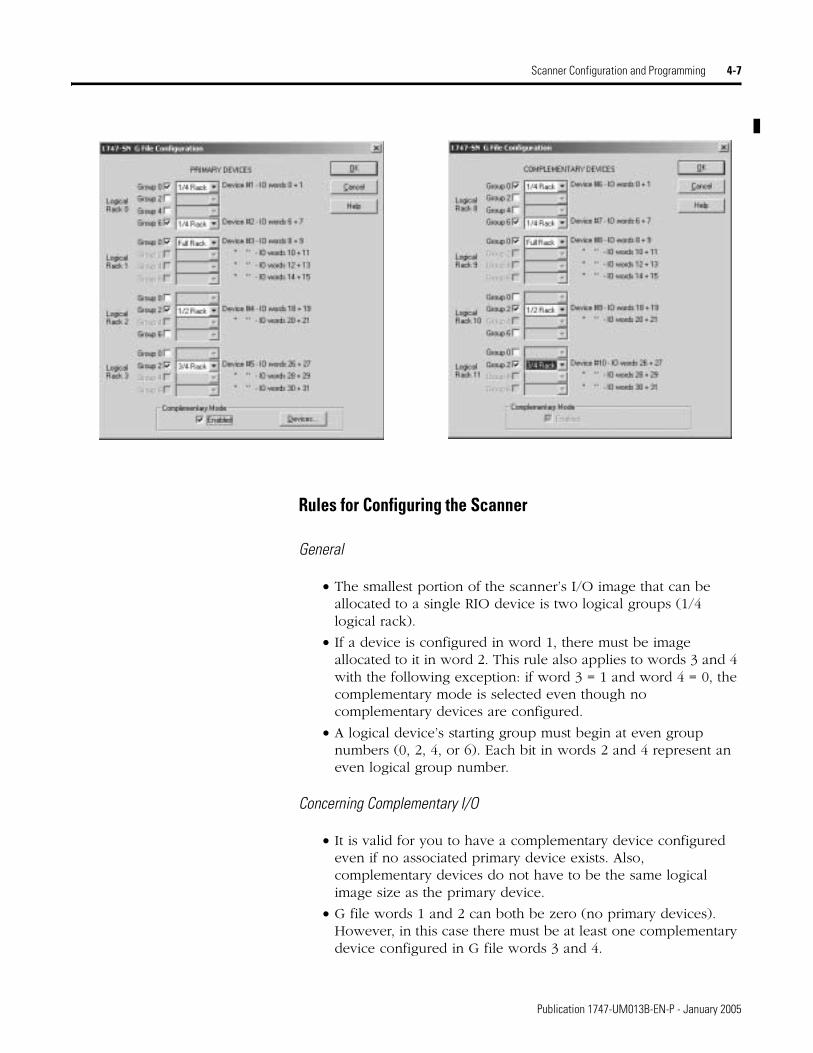
Rules for Configuring the Scanner
General
• The smallest portion of the scanner’s I/O image that can be allocated to a single RIO device is two logical groups (1/4 logical rack).
• If a device is configured in word 1, there must be image allocated to it in word 2. This rule also applies to words 3 and 4 with the following exception: if word 3 = 1 and word 4 = 0, the complementary mode is selected even though no complementary devices are configured.
• A logical device’s starting group must begin at even group numbers (0, 2, 4, or 6). Each bit in words 2 and 4 represent an even logical group number.
Concerning Complementary I/O
• It is valid for you to have a complementary device configured even if no associated primary device exists. Also, complementary devices do not have to be the same logical image size as the primary device.
• G file words 1 and 2 can both be zero (no primary devices). However, in this case there must be at least one complementary device configured in G file words 3 and 4.
Publication 1747-UM013B-EN-P - January 2005
4-8 Scanner Configuration and Programming
• If there is at least one primary device configured in G file words 1 and 2, words 3 and 4 can both be zero, or the G file size can be set to 3 (complementary mode not selected).
• The starting group of the primary and complementary chassis should be the same if they share the same image space. If the starting group is not the same, the image of the complementary device must not “cross over” into the space of a primary device.
For example, if a primary device exists at Logical Rack 1 Logical Group 4, the maximum size of a complementary device at Logical Rack 9 Logical Group 0 is a half logical rack, so its image does not cross over into Logical Group 4.
• A complementary device cannot be configured at locations where primary devices are configured unless they both start at the same location.
• If you configure your system so that complementary I/O is not selected (words 3 and 4 are zero), you must not set up any of the actual devices to be in the primary mode. If you do, the system will flag the device as faulted and prevent the device from running.
• Control functions (i.e., device inhibit, device reset, and device output reset) are only selectable for the primary device, but also apply to the complementary device. Control functions for complementary devices cannot be exclusively enabled.
Example G File Showing Primary and Complementary Device Configurations
In the example that follows, we configured the scanner to communicate with primary and complementary devices. These are the device addresses and image sizes:
• Logical Racks 0/8, Logical Group 2 contain a primary 3/4 logical rack device, and a complementary 3/4 logical rack device.
• Logical Racks 1/9, Logical Group 0 contain no primary device, and a complementary 1/2 logical rack device.
• Logical Racks 1/9, Logical Group 6 contain a primary 1/4 logical rack device, and a complementary 1/4 logical rack device.
• Logical Racks 2/10, Logical Group 0 contain a primary 3/4 logical rack device, and a complementary 1/4 logical rack device.
• Logical Racks 3/11, Logical Group 2 contain a primary 1/4 logical rack device, and a complementary 1/2 logical rack device.
• Logical Racks 3/11, Logical Group 6 contain a primary 1/4 logical rack device, and no complementary device.
Publication 1747-UM013B-EN-P - January 2005

Scanner Configuration and Programming 4-9
0
0123456789101112131415
0000010000000100
010000110000101
0111000111100101
Bit Number
024602460246
RIO Logical Rack 3Starting Logical Group
0246
I/O Mix, Word 0
G File
RIO Rack 0 Image Size
0246
RIO Rack 1Image Size
0246
RIO Rack 2Image Size
0246
RIO Rack 3Image Size
0246
RIO Logical Rack 2Starting Logical Group
RIO Logical Rack 1Starting Logical Group
RIO Logical Rack 0Starting Logical Group
0 010100110000100
0111110110000110
024602460246
RIO Logical Rack 1 1Starting Logical Group
0246
RIO Rack 8 Image Size
0246
RIO Rack 9Image Size
0246
RIO Rack 10Image Size
0246
RIO Rack 1 1Image Size
0246
RIO Logical Rack 10Starting Logical Group
RIO Logical Rack 9Starting Logical Group
RIO Logical Rack 8Starting Logical Group
Primary/Normal Logical Device Address,Word 1
Primary/Normal Logical Image Size,Word 2
Complementary Logical Device Address,Word 3
Complementary Logical Image Size,Word 4
Publication 1747-UM013B-EN-P - January 2005

4-10 Scanner Configuration and Programming
Illegal Configuration Examples
Having a primary device configured at Logical Rack 1, Logical Group 2 (bit 5) would be illegal since this image space is already being used by a complementary device. Having a complementary device configured at Logical Rack 10, Logical Group 2 (bit 9) would also be illegal since this image space is already being used by a primary device.
Note that the complementary device at Logical Rack 8, Logical Group 2 could be an ASB using 10 words (1-1/4 logical racks) of data, and thereby cross into RIO Logical Rack 9.
The G file configuration on page 2-6 would provide the primary and complementary input images to the scanner, which are illustrated on the following pages. Note that the output images would be the same.
Example Scanner Input Image of the Primary Devices
Below are the primary device addresses and sizes. The following page contains complementary device addresses and sizes.
• Device 1 - starting at Logical Rack 0, Logical Group 2 is a primary 3/4 logical rack device.
• Logical Rack 1, Logical Group 0 contains no primary device.
• Device 2 - starting at Logical Rack 1, Logical Group 6 is a primary 1/4 logical rack device.
• Device 3 - starting at Logical Rack 2, Logical Group 0 is a primary 3/4 logical rack device.
• Device 4 - starting at Logical Rack 3, Logical Group 2 is a primary 1/4 logical rack device.
• Device 5 - starting at Logical Rack 3, Logical Group 6 is a primary 1/4 logical rack device.
Publication 1747-UM013B-EN-P - January 2005

Scanner Configuration and Programming 4-11
Example Scanner Input Image of the Complementary Devices
Below are the complementary device addresses and sizes. The previous page contains primary device addresses and sizes.
• Device 6 - starting at Logical Rack 8, Logical Group 2 is a complementary 3/4 logical rack device.
• Device 7 - starting at Logical Rack 9, Logical Group 0 is a complementary 1/2 logical rack device.
• Device 8 - starting at Logical Rack 9, Logical Group 6 is a complementary 1/4 logical rack device.
• Device 9 - starting at Logical Rack 10, Logical Group 0 is a complementary 1/4 logical rack device.
• Device 10 - starting at Logical Rack 11, Logical Group 2 is a complementary 1/2 logical rack device.
• Logical Rack 11, Logical Group 6 has no complementary device.
Logical Rack 3 Group 6
Logical Rack 3 Group 7
Logical Rack 1 Group 2
Logical Rack 1 Group 3
Logical Rack 1 Group 0
Logical Rack 1 Group 1
Logical Rack 1 Group 6
Logical Rack 1 Group 4Logical Rack 1 Group 5
Logical Rack 0 Group 6
Logical Rack 0 Group 7
Logical Rack 0 Group 4
Logical Rack 0 Group 5
Logical Rack 0 Group 2
Logical Rack 0 Group 3
0123456789101112131415Bit Number (decimal) SLC InputFile Address
I:e.0
I:e.1
I:e.2
I:e.3
I:e.4I:e.5
I:e.6
I:e.7
I:e.8
I:e.9
I:e.10
I:e.1 1
I:e.12
I:e.13
I:e.14
I:e.30
I:e.31
Word 0
Word 1
Word 2
Word 3
Word 4
Word 7
Word 8
Word 9
Word 10
Word 11
Word 12Word 13Word 14
Word 5Word 6
Word 30
Word 31
Logical Rack 0 Group 0
Logical Rack 0 Group 1
Logical Rack 3 Group 1
Logical Rack 3 Group 2
Logical Rack 2 Group 7
Logical Rack 3 Group 0
Logical Rack 3 Group 5
Logical Rack 3 Group 3
Logical Rack 3 Group 4
Logical Rack 2 Group 5Logical Rack 2 Group 6
Logical Rack 2 Group 3
Logical Rack 2 Group 4
Logical Rack 2 Group 1Logical Rack 2 Group 2
I:e.15I:e.16
I:e.17
I:e.18
I:e.19I:e.20
I:e.21
I:e.22
I:e.23
I:e.24
I:e.25
I:e.26
I:e.27
I:e.28
I:e.29
Word 15
Word 16
Word 17Word 18
Word 19
Word 22
Word 23
Word 24
Word 25
Word 26
Word 27
Word 28
Word 29
Word 20Word 21
Logical Rack 1 Group 7
Logical Rack 2 Group 0
LogicalRack 0
LogicalRack 1
LogicalRack 2
LogicalRack 3
081828384858687810 811 812 813 814 815 816 817 8Bit Number (octal)
e = slot number of the SLC chassis containing the scanner
Device 1
Device 5
Device 2
Device 3
Device 4
= not used
Publication 1747-UM013B-EN-P - January 2005
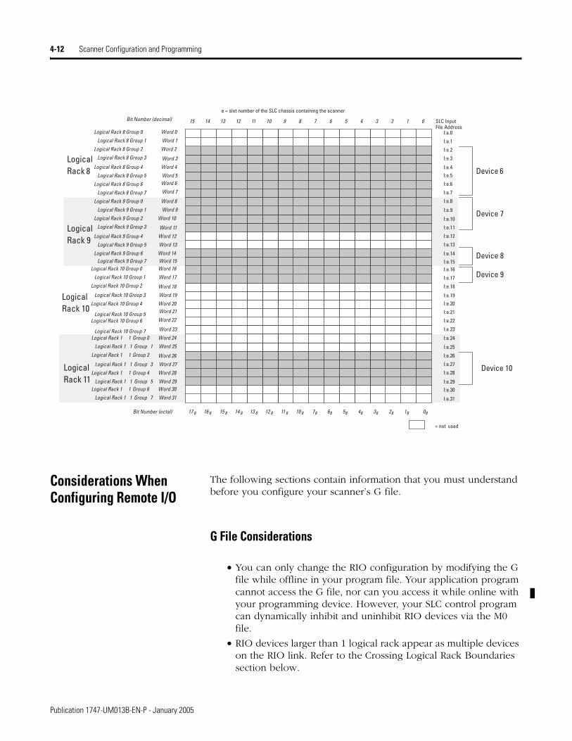
4-12 Scanner Configuration and Programming
Considerations When Configuring Remote I/O
The following sections contain information that you must understand before you configure your scanner’s G file.
G File Considerations
• You can only change the RIO configuration by modifying the G file while offline in your program file. Your application program cannot access the G file, nor can you access it while online with your programming device. However, your SLC control program can dynamically inhibit and uninhibit RIO devices via the M0 file.
• RIO devices larger than 1 logical rack appear as multiple devices on the RIO link. Refer to the Crossing Logical Rack Boundaries section below.
Logical Rack 1 1 Group 6
Logical Rack 1 1 Group 7
Logical Rack 9 Group 2
Logical Rack 9 Group 3
Logical Rack 9 Group 0
Logical Rack 9 Group 1
Logical Rack 9 Group 6
Logical Rack 9 Group 4
Logical Rack 9 Group 5
Logical Rack 8 Group 6
Logical Rack 8 Group 7
Logical Rack 8 Group 4
Logical Rack 8 Group 5
Logical Rack 8 Group 2
Logical Rack 8 Group 3
0123456789101112131415Bit Number (decimal) SLC InputFile Address
I:e.0
I:e.1
I:e.2
I:e.3
I:e.4I:e.5
I:e.6
I:e.7
I:e.8
I:e.9
I:e.10
I:e.11
I:e.12
I:e.13
I:e.14
I:e.30
I:e.31
Word 0
Word 1
Word 2
Word 3
Word 4
Word 7
Word 8
Word 9
Word 10
Word 11
Word 12
Word 13
Word 14
Word 5Word 6
Word 30
Word 31
Logical Rack 8 Group 0
Logical Rack 8 Group 1
Logical Rack 1 1 Group 1
Logical Rack 1 1 Group 2
Logical Rack 10 Group 7Logical Rack 1 1 Group 0
Logical Rack 1 1 Group 5
Logical Rack 1 1 Group 3
Logical Rack 1 1 Group 4
Logical Rack 10 Group 5Logical Rack 10 Group 6
Logical Rack 10 Group 3
Logical Rack 10 Group 4
Logical Rack 10 Group 1
Logical Rack 10 Group 2
I:e.15I:e.16
I:e.17
I:e.18
I:e.19I:e.20
I:e.21
I:e.22
I:e.23
I:e.24
I:e.25
I:e.26
I:e.27
I:e.28
I:e.29
Word 15Word 16
Word 17
Word 18
Word 19
Word 22
Word 23
Word 24
Word 25
Word 26
Word 27
Word 28
Word 29
Word 20Word 21
Logical Rack 9 Group 7Logical Rack 10 Group 0
LogicalRack 8
LogicalRack 9
LogicalRack 10
LogicalRack 11
081828384858687810 811 812 813 814 815 816 817 8Bit Number (octal)
e = slot number of the SLC chassis containing the scanner
Device 6
Device 7
Device 8
Device 9
Device 10
= not used
Publication 1747-UM013B-EN-P - January 2005
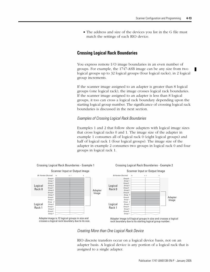
Scanner Configuration and Programming 4-13
• The address and size of the devices you list in the G file must match the settings of each RIO device.
Crossing Logical Rack Boundaries
You express remote I/O image boundaries in an even number of groups. For example, the 1747-ASB image can be any size from two logical groups up to 32 logical groups (four logical racks), in 2 logical group increments.
If the scanner image assigned to an adapter is greater than 8 logical groups (one logical rack), the image crosses logical rack boundaries. If the scanner image assigned to an adapter is less than 8 logical groups, it too can cross a logical rack boundary depending upon the starting logical group number. The significance of crossing logical rack boundaries is discussed in the next section.
Examples of Crossing Logical Rack Boundaries
Examples 1 and 2 that follow show adapters with logical image sizes that cross logical racks 0 and 1. The image size of the adapter in example 1 consumes all of logical rack 0 (eight logical groups) and half of logical rack 1 (four logical groups). The image size of the adapter in example 2 consumes two groups in logical rack 0 and four groups in logical rack 1.
Creating More than One Logical Rack Device
RIO discrete transfers occur on a logical device basis, not on an adapter basis. A logical device is any portion of a logical rack that is assigned to a single adapter.
Bit Number (Decimal)
LogicalRack 1
07815
Scanner Input or Output Image
LogicalRack 0
Group 2Group 3
Group 0Group 1
Group 6
Group 4Group 5
Bit Number (Decimal)
Group 7
LogicalRack 1
07815
Scanner Input or Output Image
Group 7
Group 5Group 6
Group 3Group 4
Group 1Group 2
Group 0
LogicalRack 0
Adapter image is 12 logical groups in size andcrosses a logical rack boundary due to its size.
Adapter image is 6 logical groups in size and crosses a logicalrack boundary due to its starting logical group number..
Group 2Group 3
Group 0Group 1
Group 6
Group 4Group 5
Group 7
Group 7
Group 5Group 6
Group 3Group 4
Group 1Group 2
Group 0
AdapterImage
AdapterImage
Crossing Logical Rack Boundaries - Example 1 Crossing Logical Rack Boundaries - Example 2
Publication 1747-UM013B-EN-P - January 2005

4-14 Scanner Configuration and Programming
When the scanner image assigned to an adapter is more than one logical device, the scanner sees the single physical device as multiple logical devices on the RIO link. The scanner communicates with each logical device independently, even if the logical devices are all assigned to one adapter. If a physical device image is more than one logical device, the following is true:
• The scanner does not update all of the adapter image at the same time. The number of logical devices determines the number of RIO discrete transfers that are needed to update the entire adapter image.
• The adapter may receive different communication commands for each logical device. In this case, the adapter decides which command it responds to.
Understanding M Files M Files Overview
The scanner provides RIO device control and status information through the M0 and M1 files. The M0 file is a control file. The M1 file is a status file
The SLC processor does not automatically update M file data during the end of the program scan as it does I/O scans. Instead, M file values act as interrupts and are immediately read from or written to upon the execution of the ladder logic instruction in which they are used. When M file data (bits or words) is addressed in the ladder program, the processor stops scanning the program to read or write the M file data to/from the scanner module. M file bits/words in the ladder program will, therefore, impact the ladder scan time. If scan time is critical, it is better to set binary file bits and copy them all at once to the M0 file, or copy a portion of the M1 file to a binary file and then address the binary file in the program. Refer to the ladder example that follows. For more information on M files, refer to
Group 2Group 3
Group 0Group 1
Group 6
Group 4Group 5
Group 7
LogicalRack 1
Group 7
Group 5Group 6
Group 3Group 4
Group 1Group 2
Group 0
LogicalRack 0 Adapter
Image
LogicalDevice
LogicalDevice
Bit Number (Decimal) 07815
Scanner Input or Output Image
In this example the adapter is configured to start at Logical Rack 0, Logical Group 0, and uses 14 words of I/O image. Note that two RIO discrete transfers are required for the scanner to update the adapter image containing two logical devices.
Publication 1747-UM013B-EN-P - January 2005

Scanner Configuration and Programming 4-15
Appendix B. You can find M file information relating to Block Transfer operations in Chapter 5, Block Transfer.
Rung 2:0To decrease program scan time, copy the first four words of the M1 Fileto a binary file and use these addresses throughout the program to accessblock transfer done, error, data, etc. information without interruptingthe program scan many times.| +COP±±±±±±±±±±±±±±±±+ |±±±±±±±±±±±±±±±±±±±±±±±±±±±±±±±±±±±±±±±±±±±±±±±±±+COPY FILE +±| | |Source #M1:1.100| | |Dest #B3:0| | |Length 4| | +±±±±±±±±±±±±±±±±±±±+
Rung 2:1Examine B3/13 (B3:0/13), an internal storage bit, to determine when ablock transfer is done. Note that examining multiple individual M±filebits directly (every scan) can measurably increase processor scan time.| ºBT DONEº | B3 +COP±±±±±±±±±±±±±±±±+ |±±±±] [±±±±±±±±±±±±±±±±±±±±±±±±±±±±±±±±±±±±±±±±±±+COPY FILE +±| | 13 |Source #B3:10| | |Dest #N10:0| | |Length 64| | +±±±±±±±±±±±±±±±±±±±+ |
Rung 2:2Examine B3/12 (an internal storage bit) to determine if a BT erroroccurred. Buffer the BT status from B3:3 if an error does occur.| ºBT ERRORº | | B3 +MOV±±±±±±±±±±±±±±±±+ |±±±±] [±±±±±±±±±±±±±±±±±±±±±±±±±±±±±±±±±±±±±±±±±±+MOVE +±| 12 |Source B3:3| | | 0000000000000000| | |Dest N10:64| | | 0| | +±±±±±±±±±±±±±±±±±±±+
Rung 2:3| |±±±±±±±±±±±±±±±±±±±±±±±±±±±±±±±±±±±±±+END+±±±±±±±±±±±±±±±±±±±±±±±±±±±±±|
IMPORTANT If you are using an SLC 5/02 processor, M file data cannot be directly monitored. To monitor M files, you must move the M file words into an SLC file that can be monitored, e.g., an integer “N” file. SLC 5/03 or later processors allow you to monitor M files directly. However, do not address M file bits more than necessary throughout your application program. The processor accesses M files like immediate I/O. Therefore, excessive addressing of M files can greatly increase SLC processor scan time. For more information on M files, refer to Appendix B.
Publication 1747-UM013B-EN-P - January 2005

4-16 Scanner Configuration and Programming
M0 Control File Description
You can control the operation of individual devices on the RIO link with M0 word 8 through M0 word 27 (M0:e.8 through M0:e.27). Through your application program, you can use the M0 file to:
• Device Inhibit - command the 1747-SN RIO Scanner to stop scanning an RIO device by using words 8 through 11.
• Device Reset - command an RIO device’s outputs to reset while the SLC processor is in Run or Test mode by using words 16 through 19.
• Remote Output Reset - command an RIO device’s outputs to reset upon the SLC processor leaving Run mode (regardless of the RIO device’s Hold Last State setting), or while in Test mode by using words 24 through 27.
If you do not modify the Device Reset and Remote Output Reset words, the device outputs reflect the scanner output image whenever the SLC processor is in Run mode. If the SLC processor is in Program, Test, or Fault mode, it instructs the device to reset its outputs.
M file data is nonretentive. Upon entering Run or Test modes, the SLC processor sets the M0 file to a default state. The processor does not use the M0 file until a full program scan occurs (after entering Run mode). This allows you to change the M file settings before they take effect.
IMPORTANT The 1747-SN RIO Scanner does not use M0 words 0 through 7.
Publication 1747-UM013B-EN-P - January 2005
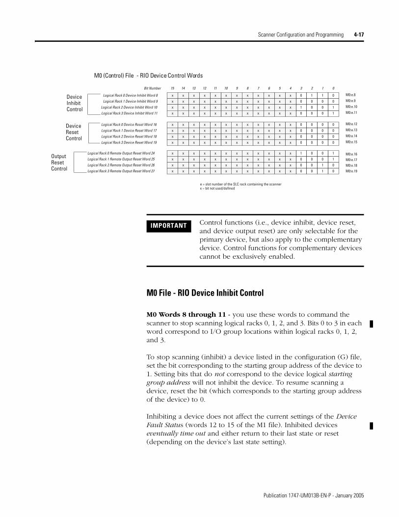
Scanner Configuration and Programming 4-17
M0 File - RIO Device Inhibit Control
M0 Words 8 through 11 - you use these words to command the scanner to stop scanning logical racks 0, 1, 2, and 3. Bits 0 to 3 in each word correspond to I/O group locations within logical racks 0, 1, 2, and 3.
To stop scanning (inhibit) a device listed in the configuration (G) file, set the bit corresponding to the starting group address of the device to 1. Setting bits that do not correspond to the device logical starting group address will not inhibit the device. To resume scanning a device, reset the bit (which corresponds to the starting group address of the device) to 0.
Inhibiting a device does not affect the current settings of the Device Fault Status (words 12 to 15 of the M1 file). Inhibited devices eventually time out and either return to their last state or reset (depending on the device’s last state setting).
0123456789101112131415Bit Number
0110xxxxxxxxxxxxLogical Rack 0 Device Inhibit Word 8
0000xxxxxxxxxxxx
1001xxxxxxxxxxxx
1000xxxxxxxxxxxx
Logical Rack 1 Device Inhibit Word 9
Logical Rack 2 Device Inhibit Word 10
Logical Rack 3 Device Inhibit Word 11
0000xxxxxxxxxxxxLogical Rack 0 Device Reset Word 16
0000xxxxxxxxxxxx
0000xxxxxxxxxxxx
0000xxxxxxxxxxxx
Logical Rack 1 Device Reset Word 17
Logical Rack 2 Device Reset Word 18
Logical Rack 3 Device Reset Word 19
1001xxxxxxxxxxxxLogical Rack 0 Remote Output Reset Word 24
1000xxxxxxxxxxxx
0100xxxxxxxxxxxx
0100xxxxxxxxxxxx
Logical Rack 1 Remote Output Reset Word 25
Logical Rack 2 Remote Output Reset Word 26
Logical Rack 3 Remote Output Reset Word 27
M0 (Control) File - RIO Device Control Words
e = slot number of the SLC rack containing the scannerx = bit not used/defined
DeviceInhibitControl
DeviceResetControl
OutputResetControl
M0:e.8
M0:e.9
M0:e.10
M0:e.11
M0:e.12
M0:e.13
M0:e.14
M0:e.15
M0:e.16M0:e.17M0:e.18M0:e.19
IMPORTANT Control functions (i.e., device inhibit, device reset, and device output reset) are only selectable for the primary device, but also apply to the complementary device. Control functions for complementary devices cannot be exclusively enabled.
Publication 1747-UM013B-EN-P - January 2005

4-18 Scanner Configuration and Programming
Default: When the processor enters the Run mode, the scanner automatically inhibits any device not configured in the G file (bit set to 1). Attempting to inhibit an unconfigured device has no effect.
Example of Device Inhibit Control
The 1747-SN Scanner inhibits (sets to 1) the bits in M0:e.8 through M0:e.11 (by default) wherever there are no configured devices present. The illustration below compares the configured devices (G file word 2) to the groups that the scanner automatically inhibits.
M0 File - RIO Device Reset Control
M0 Words 16 through 19 - you use these words to command a reset (0) of RIO device outputs when the SLC processor is in Run or Test mode. This allows you to selectively reset logical device outputs based on a previous condition(s) that you defined. Bits 0 to 3 correspond to the logical I/O group locations within logical racks 0, 1, 2, and 3.
To command an RIO device to a reset (0) condition (from Run or Test mode), set the bit corresponding to the starting logical address of the device to 1. Setting bits that do not correspond to a device starting
M0 File0110xxxxxxxxxxxxLogical Rack 0 Device Inhibit Word 8 M0:e.80000xxxxxxxxxxxx M0:e.91001xxxxxxxxxxxx M0:e.101000xxxxxxxxxxxx M0:e.11
Logical Rack 1 Device Inhibit Word 9
Logical Rack 2 Device Inhibit Word 10
Logical Rack 3 Device Inhibit Word 11
0123456789101112131415Bit Number (decimal)
M0 (Control) File Words 8 through 11
e = slot number of the SLC rack containing the scannerx = not used/defined
Not Defined
Starting Group0246
0123456789101112131415 M0 File0110xxxxxxxxxxxx M0:e.80000xxxxxxxxxxxx M0:e.91001xxxxxxxxxxxx M0:e.101000xxxxxxxxxxxx M0:e.11
M0 (Control) File
RIO Logical Rack 0Starting Group
0246
RIO Logical Rack 1Starting Group
0246
RIO Logical Rack 2Starting Group
0246
RIO Logical Rack 3Starting Group
0246
G File
1001111101100111Device Address, Word 1
Bit Number (decimal)Logical Rack 0 Device Inhibit Word 8
Logical Rack 1 Device Inhibit Word 9
Logical Rack 2 Device Inhibit Word 10
Logical Rack 3 Device Inhibit Word 11
e = slot number of the SLC rack containing the scannerx = not used/defined
Publication 1747-UM013B-EN-P - January 2005
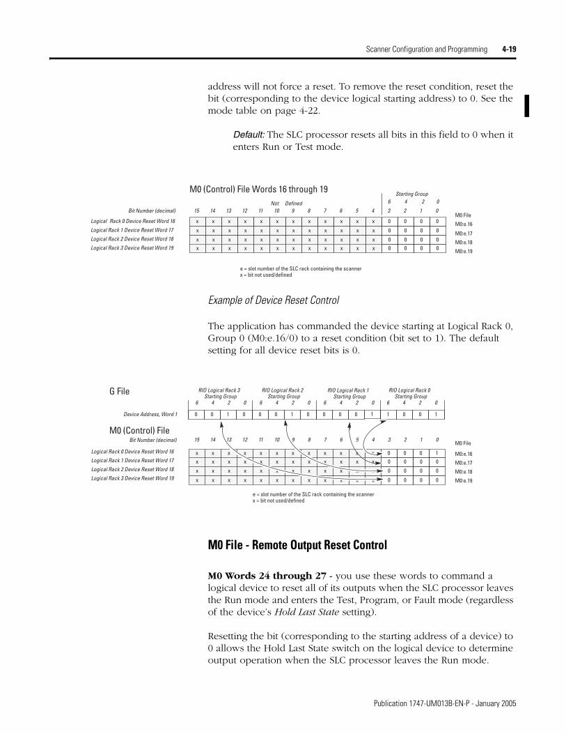
Scanner Configuration and Programming 4-19
address will not force a reset. To remove the reset condition, reset the bit (corresponding to the device logical starting address) to 0. See the mode table on page 4-22.
Default: The SLC processor resets all bits in this field to 0 when it enters Run or Test mode.
Example of Device Reset Control
The application has commanded the device starting at Logical Rack 0, Group 0 (M0:e.16/0) to a reset condition (bit set to 1). The default setting for all device reset bits is 0.
M0 File - Remote Output Reset Control
M0 Words 24 through 27 - you use these words to command a logical device to reset all of its outputs when the SLC processor leaves the Run mode and enters the Test, Program, or Fault mode (regardless of the device’s Hold Last State setting).
Resetting the bit (corresponding to the starting address of a device) to 0 allows the Hold Last State switch on the logical device to determine output operation when the SLC processor leaves the Run mode.
M0 File0123456789101112131415Bit Number (decimal)
M0 (Control) File Words 16 through 19
Logical Rack 0 Device Reset Word 16 M0:e.160000xxxxxxxxxxxx M0:e.170000xxxxxxxxxxxx M0:e.180000xxxxxxxxxxxx M0:e.19
Logical Rack 1 Device Reset Word 17
Logical Rack 2 Device Reset Word 18
Logical Rack 3 Device Reset Word 19
e = slot number of the SLC rack containing the scannerx = bit not used/defined
0000xxxxxxxxxxxx
Not Defined
Starting Group0246
0000xxxxxxxxxxxx
0000xxxxxxxxxxxx
0000xxxxxxxxxxxx
1000xxxxxxxxxxxx
0123456789101112131415M0 File
M0:e.16
M0:e.17
M0:e.18
M0:e.19
1 100100001000100Device Address, Word 1
G File
M0 (Control) FileBit Number (decimal)
e = slot number of the SLC rack containing the scannerx = bit not used/defined
Logical Rack 0 Device Reset Word 16
Logical Rack 1 Device Reset Word 17
Logical Rack 2 Device Reset Word 18
Logical Rack 3 Device Reset Word 19
RIO Logical Rack 0Starting Group
0246
RIO Logical Rack 1Starting Group
0246
RIO Logical Rack 2Starting Group
0246
RIO Logical Rack 3Starting Group
0246
Publication 1747-UM013B-EN-P - January 2005
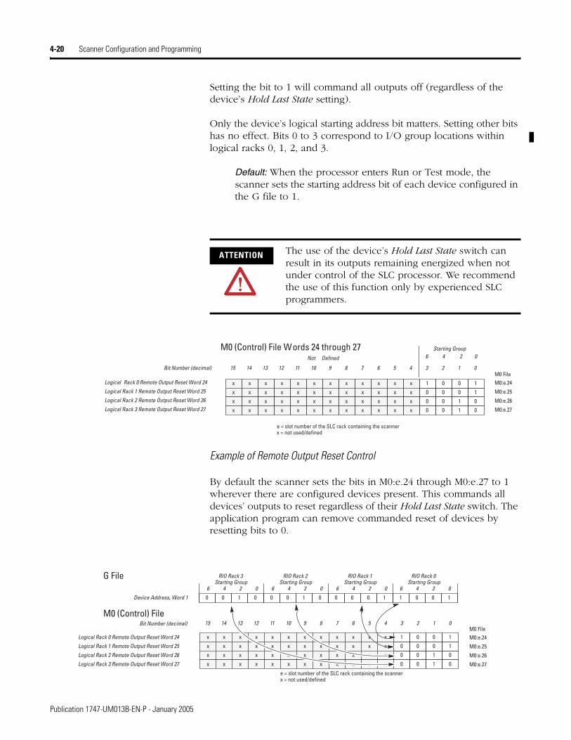
4-20 Scanner Configuration and Programming
Setting the bit to 1 will command all outputs off (regardless of the device’s Hold Last State setting).
Only the device’s logical starting address bit matters. Setting other bits has no effect. Bits 0 to 3 correspond to I/O group locations within logical racks 0, 1, 2, and 3.
Default: When the processor enters Run or Test mode, the scanner sets the starting address bit of each device configured in the G file to 1.
Example of Remote Output Reset Control
By default the scanner sets the bits in M0:e.24 through M0:e.27 to 1 wherever there are configured devices present. This commands all devices’ outputs to reset regardless of their Hold Last State switch. The application program can remove commanded reset of devices by resetting bits to 0.
ATTENTION The use of the device’s Hold Last State switch can result in its outputs remaining energized when not under control of the SLC processor. We recommend the use of this function only by experienced SLC programmers.
M0 File0123456789101112131415Bit Number (decimal)
M0 (Control) File Words 24 through 27
Logical Rack 0 Remote Output Reset Word 24 M0:e.24
M0:e.25
M0:e.26
M0:e.27
Logical Rack 1 Remote Output Reset Word 25
Logical Rack 2 Remote Output Reset Word 26
Logical Rack 3 Remote Output Reset Word 27
e = slot number of the SLC rack containing the scannerx = not used/defined
Not Defined
Starting Group0246
1001xxxxxxxxxxxx
1000xxxxxxxxxxxx
0100xxxxxxxxxxxx
0100xxxxxxxxxxxx
1001xxxxxxxxxxxx
1000xxxxxxxxxxxx
0100xxxxxxxxxxxx
0100xxxxxxxxxxxx
0123456789101112131415M0 FileM0:e.24
M0:e.25
M0:e.26
M0:e.27
1 100100001000100Device Address, Word 1
G File RIO Rack 0Starting Group
0246
RIO Rack 1Starting Group
0246
RIO Rack 2Starting Group
0246
RIO Rack 3Starting Group
0246
M0 (Control) FileBit Number (decimal)
Logical Rack 0 Remote Output Reset Word 24
Logical Rack 1 Remote Output Reset Word 25
Logical Rack 2 Remote Output Reset Word 26
Logical Rack 3 Remote Output Reset Word 27
e = slot number of the SLC rack containing the scannerx = not used/defined
Publication 1747-UM013B-EN-P - January 2005
Scanner Configuration and Programming 4-21
Device Reset and Remote Output Reset Considerations
The 1747-SN Scanner Device Reset words (M0:e.16 to M0:e.19) and the Remote Output Reset words (M0:e.24 to M0:e.27) operate in conjunction with each RIO device to determine the state of that RIO device’s outputs. The output control information that the scanner sends to the RIO device depends on how you configure these bits. The RIO device acts on the output control information in accordance with its functionality and configuration. To fully understand how a specific device responds to the Device Reset and Remote Output Reset words, you must determine the operation of the RIO device. To determine RIO device output operation, refer to that device’s user manual.
To properly use the Device Reset and Remote Output Reset words, you must consider the output control information sent to the devices during two SLC processor operating conditions:
• The SLC processor is in any given mode (Run, Program, Test, or Fault).
• The SLC processor is leaving any mode and entering another.
If you do not modify the Device Reset and Remote Output Reset words, the device outputs reflect the scanner output image whenever the SLC processor is in Run mode. If the SLC processor is in Program, Test, or Fault mode, it instructs the device to reset its outputs.
If you modify the default settings, the Device Reset and Remote Output Reset words change. The table on the following page contains examples of what changes occur. We base the information in the table on the assumption that the scanner’s slot is always enabled and the RIO link device is communicating with the scanner.
To determine how the Device Reset and Remote Output Reset words operate, locate the box where the row and column are headed by the modes in question. The shaded boxes represent the Device Reset and Remote Output Reset word operation while in that mode.
Example 1 - When powering up into Run mode, the scanner, by default, resets the appropriate bit in the Device Reset word to 0. The appropriate bit in the Remote Output Reset word is set to 1. As a result, the RIO link device outputs reflect the scanner’s output image.
ATTENTION When using the Device Reset and Remote Output Reset words, you must completely understand and fully test all device output operations before beginning normal system operation.
Publication 1747-UM013B-EN-P - January 2005
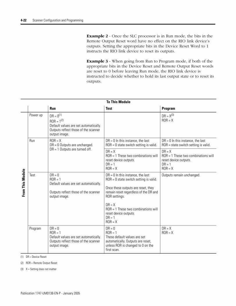
4-22 Scanner Configuration and Programming
Example 2 - Once the SLC processor is in Run mode, the bits in the Remote Output Reset word have no effect on the RIO link device’s outputs. Setting the appropriate bits in the Device Reset Word to 1 instructs the RIO link device to reset its outputs.
Example 3 - When going from Run to Program mode, if both of the appropriate bits in the Device Reset and Remote Output Reset words are reset to 0 before leaving Run mode, the RIO link device is instructed to decide whether to hold its last output state or to reset its outputs.
To This Module
Run Test Program
From
Thi
s M
odul
e
Power up DR = 0(1)
ROR = 1(2)
Default values are set automatically. Outputs reflect those of the scanner output image.
DR = X(3)
ROR = X
Run ROR = XDR = 0 Outputs are unchanged.DR = 1 Outputs are turned off.
DR = 0 In this instance, the lastROR = 0 state switch setting is valid.
DR = 0 In this instance, the lastROR = state switch setting is valid.
DR = XROR = 1 These two combinations will reset device outputs.DR = 1ROR = X
DR = XROR = 1 These two combinations will reset device outputs.DR = 1ROR = X
Test DR = 0ROR = 1Default values are set automatically.
Outputs reflect those of the scanner output image.
DR = 0 In this instance, the lastROR = 0 state switch setting is valid.
Once these outputs are reset, they remain reset regardless of the DR and ROR settings.
DR = XROR = 1 These two combinations will reset device outputs.DR = 1ROR = X
Outputs remain unchanged.
Program DR = 0ROR = 1Default values are set automatically. Outputs reflect those of the scanner output image.
DR = 0ROR = 1These default values are set automatically. Outputs are reset, unless ROR is changed to 0 on the first scan.
DR = XROR = X
(1) DR = Device Reset
(2) ROR = Remote Output Reset
(3) X = Setting does not matter
Publication 1747-UM013B-EN-P - January 2005

Scanner Configuration and Programming 4-23
M1 Status File Description M1 file words 0 through 47 contain the status of all devices on the scanner’s RIO link. M1 is a read only file; do not write to this file.
Words 0 to 47 of the M1 file provide the following information:
• Word 0 (M1:e.0) - general communication status (overall device fault and communications attempted)
• Word 2 (M1:e.2) - RIO baud rate status
• Word 3 (M1:e.3) - complementary device starting address status
• Word 4 (M1:e.4) - complementary logical image size status
• Word 5 (M1:e.5) - complementary active device status
• Word 8 (M1:e.8) - primary/normal device starting address status
• Word 9 (M1:e.9) - primary/normal logical image size status
• Word 10 (M1:e.10) - active device status
• Words 12-15 (M1:e.12 -15) - device fault status
• Words 16-31 (M1:e.16-31) - primary/normal device retry counters
• Words 32-47 (M1:e.32-47) - complementary device retry counters
General Communication Status - Enable Device Fault Bit
Word 0, bit 0 - is the Enabled Device Fault status bit. When any enabled device is faulted, this bit is set to 1. A fault may be caused by a communication problem with a remote device.
General Communication Status - Communication Attempted Bit
Word 0, bit 1 - is the Communications Attempted status bit. When RIO communication has been attempted with all configured devices, this bit is set to 1. There are no further transitions of this bit until a processor change of state occurs (i.e., Program mode to Run mode or Test mode, or Test mode to Run mode).
Until this bit is set, all devices in M1 file word 10 (active device status) appear to be inactive. This bit can be used to condition the Enabled
0123456789101112131415
11xxxxxxxxxxxxxxGeneral Communication Status Word, Word 0 M1:e.0
M1 File
M1 (Status) File Word 0
Enabled DeviceFault Bit
Bit Number (decimal)
Publication 1747-UM013B-EN-P - January 2005

4-24 Scanner Configuration and Programming
Device Fault bit. If the Communications Attempted bit is 1, the Enabled Device Fault bit is valid.
RIO Baud Rate Status
Word 2, bits 0 to 1 - displays the RIO communication/baud rate you have set the scanner to via its DIP switch. Writing to word 2 does not change the scanner baud rate.
As illustrated by the table below, bit 0 = SW1 and bit 1 = SW2.
Logical Device Starting Address Status
Word 8 - provides status/feedback of the logical device starting addresses you configured in word 1 of the G file (primary/normal logical devices). Writing to M1 file word 8 will not alter the contents of the G file.
0123456789101112131415
11xxxxxxxxxxxxxx M1:e.0
M1 File
CommunicationsAttemptedStatus Bit
Bit Number (decimal)
M1 (Status) File Word 0
General Communication Status Word, Word 0
Enable DeviceFault Bit
0123456789101112131415
10xxxxxxxxxxxxxxRIO Baud Rate, Word 2M1 FileM1:e.2
Baud Rate
M1 (Status) File - Word 2Bit Number (decimal)
Bit 1 - 0 Baud Rate SW 1 - 2
11 57.6K Baud 11
01 115.2K Baud 10
10 230.4K Baud 01
00 230.4K Baud 00
Publication 1747-UM013B-EN-P - January 2005

Scanner Configuration and Programming 4-25
Word 3 - provides status/feedback of the logical device starting addresses you configured in word 3 of the G file (complementary devices). Writing to M1 file word 3 will not alter the contents of the G file.
Logical Device Image Size Status
Word 9 - provides status/feedback of the logical device image size you configure in word 2 of the G file (primary/normal devices). A bit set to 1 shows the logical image size of each logical device. Writing to word M1 file word 9 will not alter the contents of the G file.
1
Primary Logical Device Address, Word 8 M1:e.8
M1 (Status) File - W ord 8
1 100100001000100
G File - W ord 1
1 10010000100000 Primary Logical Device Address, Word 1
0123456789101112131415M1 File
Bit Number (decimal)
RIO Logical Rack 3Starting Group 2
RIO Logical Rack 2Starting Group 2
RIO Logical Rack 1Starting Group 0
RIO Logical Rack 0Starting Group 0
RIO Logical Rack 0Starting Group 6
Starting Group
0246
Starting Group
0246
Starting Group
0246
Starting Group
0246
1
Complementary Logical Device Address,Word 3
M1:e.3
M1 (Status) File - W ord 3
1 100100001000100
G File - W ord 3
1 10010000100000
0123456789101112131415M1 File
Bit Number (decimal)
RIO Logical Rack 11Starting Group 2
RIO Logical Rack 10Starting Group 2
RIO Logical Rack 9Starting Group 0
RIO Logical Rack 8Starting Group 0
RIO Logical Rack 8Starting Group 6
Starting Group
0246
Starting Group
0246
Starting Group
0246
Starting Group
0246Complementary Logical Device Address,
Word 3
RIO Rack 0Image Size
0246
RIO Rack 1Image Size
0246
RIO Rack 2Image Size
0246
RIO Rack 3Image Size
0246
0123456789101112131415M1 FilePrimary Logical Device Image Size, Word 9M1:e.9
G File - W ord 2
Primary Logical Device Image Size, Word 2
M1 (Status) File - W ord 9Bit Number (decimal)
1 100111101100111
1 100111101100111
Publication 1747-UM013B-EN-P - January 2005

4-26 Scanner Configuration and Programming
Word 4 - provides status/feedback of the logical device image size you configure in word 4 of the G file (complementary devices). A bit set to 1 shows the logical image size of each logical device. Writing to word M1 file word 4 will not alter the contents of the G file.
Active Device Status
Word 10 - provides active device status for primary/normal devices. When a RIO device is communicating with the scanner the bit corresponding to the device’s logical starting group is set to 1.
Devices that are inhibited in the M0 file (M0:e.8 through M0:e.11) are represented by a 0. Unless devices are inhibited, not responding to communications, or configured to an incorrect logical rack size, this word is identical to the device configuration (M1:e.8).
Word 5 - provides active device status for complementary devices. When a RIO device is communicating with the scanner the bit corresponding to the device’s logical starting group is set to 1.
Devices that are inhibited in the M0 file are represented by a 0. Unless devices are inhibited, not responding to communications, or configured to an incorrect logical rack size, this word is identical to the device configuration (M1:e.3).
RIO Rack 8Image Size
0246
RIO Rack 9Image Size
0246
RIO Rack 10Image Size
0246
RIO Rack 11Image Size
0246
0123456789101112131415M1 FileComplementary Logical Device Image Size, Word 4M1:e.4
G File - W ord 4
Complementary Logical Device Image Size, Word 4
M1 (Status) File - W ord 4Bit Number (decimal)
1 100111101100111
1 100111101100111
0
RIO Rack 0Starting Group
0246
RIO Rack 1Starting Group
0246
RIO Rack 2Starting Group
0246
RIO Rack 3Starting Group
0246
0123456789101112131415
M1 File
Primary Logical Device Address, Word 8 M1:e.8
Primary Logical Image Size, Word 9 M1:e.9
Primary Active Device Status, Word 10 M1:e.10
1 100100001000100
101111101100111
1001100001000000
A 0 indicates that the device isinhibited, not responding tocommunications, or configured toan incorrect logical rack size.
M1 (Status) File - Word 10
Bit Number (decimal)
A 1 indicates that the configureddevice is active.
Publication 1747-UM013B-EN-P - January 2005

Scanner Configuration and Programming 4-27
Logical Device Fault Status
Words 12 through 15, bits 0 to 7 - indicate the device fault status for logical racks 0, 1, 2, 3, 8, 9, 10, and 11. Bits 0 through 3 are for primary/normal devices and bits 4 through 7 are for complementary devices. Each bit corresponds to a quarter logical rack location. If a device is not responding to communications, has gone off line, or is configured to an incorrect logical rack size, all bits corresponding to the device will be set to 1. This is highlighted in the example below.
IMPORTANT When a primary device is inhibited, its complementary device is also inhibited. A complementary device cannot be exclusively inhibited.
0
RIO Rack 8Starting Group
0246
RIO Rack 9Starting Group
0246
RIO Rack 10Starting Group
0246
RIO Rack 1 1Starting Group
0246
0123456789101112131415
M1 File
Complementary Logical Device Address, Word 3 M1:e.3
Complementary Logical Image Size, Word 4 M1:e.4
Complementary Active Device Status, Word 5 M1:e.5
1 100100001000100
101111101100111
1001100001000000
A 0 indicates that the device isinhibited, not responding tocommunications, or configured toan incorrect logical rack size.
M1 (Status) File - W ord 5
Bit Number (decimal)
A 1 indicates that the configureddevice is active.
Publication 1747-UM013B-EN-P - January 2005

4-28 Scanner Configuration and Programming
RIO Status Example
The following example illustrates an M1 status file example. It shows a typical M1 file and the G file used to configure the scanner. There are no inhibited devices specified in the M0 file (not shown). Notice that:
• M1:e.8 is an image of word 1 (primary/normal logical device address) of the G file.
0
0123456789101112131415
M1 File
Primary Device Address, Word 8 M1:e.8
Primary Device Size, Word 9 M1:e.9
Primary Active Device Status, Word 10 M1:e.10
M1 (Status) File Primary/Normal Device Fault Status
1 100100001000100
1001111101100111
101100001000000
The information contained in words 8, 9, and 10indicates a three quarter logical rack device beginning atLogical Rack 3 Logical Group 2 is faulted or configuredto an incorrect logical rack size. This device status isconfirmed in bits 1, 2, and 3 of Device Fault Status Word15.
xxxxxxxxxxxxLogical Rack 0 Device Fault Status Word 12 M1:e.12xxxxxxxxxxxx M1:e.13xxxxxxxxxxxx M1:e.14xxxxxxxxxxxx M1:e.15
Logical Rack 1 Device Fault Status Word 13
Logical Rack 2 Device Fault Status Word 14
Logical Rack 3 Device Fault Status Word 15
000 0
000 0
000 0
111 0
RIO Rack 0Starting Group
0246
RIO Rack 1Starting Group
0246
RIO Rack 2Starting Group
0246
RIO Rack 3Starting Group
0246
e = slot number of the SLC rack containing the scannerx = not used/defined
Bit Number (decimal)
0
0123456789101112131415
M1 File
Complementary Device Address, Word 3 M1:e.3
Complementary Device Size, Word 4 M1:e.4
Complementary Active Device Status, Word 5 M1:e.5
M1 (Status) File Complementary Device Fault Status
1 100100001000100
1001111101100111
101100001000000
The information contained in word 3, 4, and 5 indicates athree quarter logical rack device beginning at group 2 isinhibited, faulted, or configured to an incorrect logicalrack size. This device status is confirmed in bits 5, 6,and 7 of Device Fault Status Word 15.
0000xxxxxxxxLogical Rack 8 Device Fault Status Word 12 M1:e.120000xxxxxxxx M1:e.130000xxxxxxxx M1:e.140111xxxxxxxx M1:e.15
Logical Rack 9 Device Fault Status Word 13
Logical Rack 10 Device Fault Status Word 14Logical Rack1 1 Device Fault Status Word 15
xxx x
xxx x
xxx x
xxx x
RIO Rack 8Starting Group
0246
RIO Rack 9Starting Group
0246
RIO Rack 10Starting Group
0246
RIO Rack 1 1Starting Group
0246
e = slot number of the SLC rack containing the scannerx = not used/defined
Bit Number (decimal)
Publication 1747-UM013B-EN-P - January 2005
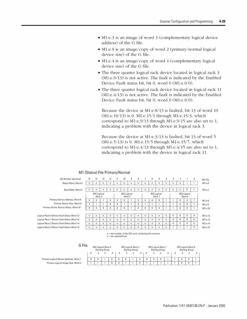
Scanner Configuration and Programming 4-29
• M1:e.3 is an image of word 3 (complementary logical device address) of the G file.
• M1:e.9 is an image/copy of word 2 (primary/normal logical device size) of the G file.
• M1:e.4 is an image/copy of word 4 (complementary logical device size) of the G file.
• The three quarter logical rack device located in logical rack 3 (M1:e.9/13) is not active. The fault is indicated by the Enabled Device Fault status bit, bit 0, word 0 (M1:e.0/0).
• The three quarter logical rack device located in logical rack 11 (M1:e.4/13) is not active. The fault is indicated by the Enabled Device Fault status bit, bit 0, word 0 (M1:e.0/0).
Because the device at M1:e.8/13 is faulted, bit 13 of word 10 (M1:e.10/13) is 0. M1:e.15/1 through M1:e.15/3, which correspond to M1:e.9/13 through M1:e.9/15 are also set to 1, indicating a problem with the device in logical rack 3.
Because the device at M1:e.3/13 is faulted, bit 13 of word 5 (M1:e.5/13) is 0. M1:e.15/5 through M1:e.15/7, which correspond to M1:e.4/13 through M1:e.4/15 are also set to 1, indicating a problem with the device in logical rack 11.
0123456789101112131415
11xxxxxxxxxxxxxx
RIO LogicalRack 0
Status Word, Word 0
RIO LogicalRack 1
RIO LogicalRack 2
RIO LogicalRack 3
10xxxxxxxxxxxxxxBaud Rate, Word 2
M1:e.0M1 File
M1:e.2
M1:e.8
M1:e.9
M1:e.10
xxxxxxxxxxxx M1:e.12xxxxxxxxxxxx M1:e.13xxxxxxxxxxxx M1:e.14xxxxxxxxxxxx M1:e.15
M1 (Status) File Primary/Normal
1 100100001000100
1001111101100111
1001100001000000
000 0
000 0
000 0
111 0
1 100100001000100
1001111101100111
RIO Logical Rack 3Starting Group
0246
Primary Logical Device Address, Word 1
Primary Logical Image Size, Word 2
e = slot number of the SLC rack containing the scannerx = not used/defined
G File
Bit Number (decimal)
RIO Logical Rack 2Starting Group
0246
RIO Logical Rack 1Starting Group
0246
RIO Logical Rack 0Starting Group
0246
Primary Device Address, Word 8
Primary Device Size, Word 9
Primary Active Device Status, Word 10
Logical Rack 0 Device Fault Status Word 12
Logical Rack 1 Device Fault Status Word 13
Logical Rack 2 Device Fault Status Word 14
Logical Rack 3 Device Fault Status Word 15
Publication 1747-UM013B-EN-P - January 2005

4-30 Scanner Configuration and Programming
RIO Communication Retry Counter (M1:e.16 -47)
M1 File Status Words 16 through 47 - indicate how many RIO communication retries the scanner makes to each adapter on the RIO link if communication problems occur. Each word (16 through 47) contains a retry counter for each configured quarter logical rack (words 16 through 31 are for primary logical racks, 0 through 3, and 32 through 47 are for complementary racks, 8 through 11). Retry counters are useful for troubleshooting communication problems (such as electrical noise or poor communication line connections) between the scanner and any adapters. The scanner clears the retry counters when going from Program to Run mode, Test to Run mode, and when going from Program to Test mode. Note that the display (in words M1:e.16 through 31) of retry counters corresponds to the bits set in the Primary Logical Device Address - Word 1 of the G file. Likewise, the display (in words M1:e.32 through 47) correspond to the bits set in the Complementary Logical Device Address - Word 3 of the G file.
0123456789101112131415
11xxxxxxxxxxxxxx
RIO LogicalRack 8
Status Word, Word 0
RIO LogicalRack 9
RIO LogicalRack 10
RIO LogicalRack 1 1
10xxxxxxxxxxxxxxBaud Rate, Word 2
M1:e.0M1 File
M1:e.2
Complementary Device Starting Address, Word 3 M1:e.3
Complementary Device Image Size, Word 4 M1:e.4
Complementary Active Device Status, Word 5 M1:e.5
0000xxxxxxxxLogical Rack 8 Device Fault Status Word 12 M1:e.120000xxxxxxxx M1:e.130000xxxxxxxx M1:e.140111xxxxxxxx M1:e.15
Logical Rack 9 Device Fault Status Word 13
Logical Rack 10 Device Fault Status Word 14
Logical Rack 11 Device Fault Status Word 15
M1 (Status) File Complementary
1 100100001000100
1001111101100111
1001100001000000
xxx x
xxx x
xxx x
xxx x
1 100100001000100
1001111101100111
RIO Logical Rack 1 1Starting Group
0246
Complementary Logical Device Address, Word 3
Complementary Logical Image Size, Word 4
e = slot number of the SLC rack containing the scannerx = not used/defined
G File
Bit Number (decimal)
RIO Logical Rack 10Starting Group
0246
RIO Logical Rack 9Starting Group
0246
RIO Logical Rack 8Starting Group
0246
IMPORTANT Individual quarter logical racks within a device cannot be faulted. Therefore, only the starting logical group of the device needs to be monitored.
Publication 1747-UM013B-EN-P - January 2005

Scanner Configuration and Programming 4-31
Retry Counter Example for Primary Devices
The scanner’s I/O image tables are configured as shown with M1 status files displaying the corresponding retry counters:
M1:e.16 - communication retry counter for RIO logical rack 0, group 0M1:e.17 - not used in this exampleM1:e.18 -communication retry counter for RIO logical rack 0, group 4M1:e.19 - not used in this example
M1:e.20 - communication retry counter for RIO logical rack 1, group 0M1:e.21 - not used in this exampleM1:e.22 - not used in this exampleM1:e.23 - not used in this example
M1:e.24 - not used in this exampleM1:e.25 - communication retry counter for RIO logical rack 2, group 2M1:e.26 - not used in this exampleM1:e.27 - not used in this example
M1:e.28 - communication retry counter for RIO logical rack 3, group 0M1:e.29 - not used in this exampleM1:e.30 - not used in this exampleM1:e.31 - communication retry counter for RIO logical rack 3, group 6
IMPORTANT Your SLC control program cannot initialize/clear retry counters.
0
0123456789101112131415
101100001001001
Bit Number
Primary Logical Device Address, Word 1
G File - P rimary
Specifies RIOaddresses forprimary logicaldevices.
RIO Logical Rack 0Starting Group
6 4 2 0 6 4 2 0 6 4 2 0 6 4 2 0
RIO Logical Rack 1Starting Group
RIO Logical Rack 2Starting Group
RIO Logical Rack 3Starting Group
0
0123456789101112131415
100100010001100
Bit Number
Complementary Logical Device Address,Word 3
G File - Comp lementary
Specifies RIOaddresses forcomplementary devices.
RIO Logical Rack 8Starting Group
6 4 2 0 6 4 2 0 6 4 2 0 6 4 2 0
RIO Logical Rack 9Starting Group
RIO Logical Rack 10Starting Group
RIO Logical Rack 1 1Starting Group
Publication 1747-UM013B-EN-P - January 2005
4-32 Scanner Configuration and Programming
M1:e.32 - communication retry counter for RIO logical rack 8, group 0M1:e.33 - not used in this exampleM1:e.34 - not used in this exampleM1:e.35 - not used in this example
M1:e.36 - communication retry counter for RIO logical rack 9, group 0M1:e.37 - not used in this exampleM1:e.38 - not used in this exampleM1:e.39 - not used in this example
M1:e.40 - communication retry counter for RIO logical rack 10, group 0
M1:e.41 - not used in this exampleM1:e.42 - not used in this exampleM1:e.43 - not used in this example
M1:e.44 - communication retry counter for RIO logical rack 11, group 0
M1:e.45 - communication retry counter for RIO logical rack 11, group 2
M1:e.46 - not used in this exampleM1:e.47 - not used in this example
Understanding Slot Addressing
This section provides information about:
• 2-slot addressing
• 1-slot addressing
• 1/2-slot addressing
Understanding slot addressing is critical to most efficiently allocate your scanner’s I/O image files.
Slot addressing refers to how each remote chassis slot is assigned a specific amount of the I/O image. The amount depends on which type of slot addressing you choose at your adapter; 2-slot, 1-slot, and 1/2-slot addressing is available, as shown below:
Publication 1747-UM013B-EN-P - January 2005
Scanner Configuration and Programming 4-33
For more information on slot addressing, refer to your ASB module user manual.
Note that slot addressing (e.g., 1/2-, 1-, and 2-slot) may not apply to all types of RIO devices. Refer to each RIO device’s user manual to determine the type of slot addressing required.
SLC/Scanner Configuration Your SLC 5/02 processor can be programmed with an HHT(1)
(Hand-Held Terminal). Although the configuration steps are similar, they are not identical. Therefore, the following basic steps are provided. For specific instructions, refer to the user manual included with your programming device. For more information on M and G files, refer to appendix B.
1. Locate an open slot in your SLC chassis. Remember that you must use an SLC 5/02 or later processor.
2-SlotAddressing
Two slots are addressed as one logical group.
1-SlotAddressing
One slot is addressed as one logical group.
1/2-SlotAddressing
One slot is addressed as two logical groups.
Slot 1
Slot 1
Slot 1Slot 2
Slot 1
Slot 1
Slot 1Slot 2
Input Image
Input Image
Input Image
Output Image
Output Image
Output Image
Remote Chassis
Remote Chassis
Remote Chassis
07815 07815
07815 07815
07815 07815
(1) The SLC 5/03 and SLC 5/04 processors cannot be programmed with the HHT.
Publication 1747-UM013B-EN-P - January 2005

4-34 Scanner Configuration and Programming
2. Assign the scanner to a physical slot in the SLC processor’s chassis by selecting Scanner from the list. If the scanner selection is not available, select OTHER from the I/O Configuration Screen and enter the Code ID number: 13608.
3. Enter the number of Scanned Input and Output Words using the Specialty I/O and Advanced Setup menus.
The default value is 32 I/O words. You can specify less than 32 and reduce the processor scan time by transferring only the part of the input and output image that your application requires.
4. Using the Specialty I/O Configuration menu, set the M1 and M0 file sizes to 32 words (48 words if using complementary I/O). 32 words is the minimum required for operation. If you do not set the M1 and M0 file sizes to at least 32 words the programming device will not allow you to access the M files in the SLC control program.
If you are using the block transfer (BT) function, you should set the M1 and M0 file sizes to 3,300. Refer to Chapter 5 before completing this selection.
5. Set the G file size to 3 (5 if using complementary I/O) using the Specialty I/O Configuration menu.
6. Enter your setup information using the Modify G File menu.
IMPORTANT Do not set either of these values to 0. If you do, the scanner will not work correctly.
IMPORTANT SLC 5/02 processors scan chassis I/O slots left to right starting at slot 1, regardless of the module type. SLC 5/03 and later processors scan slots with discrete I/O modules first, left to right starting at slot 1, and then slots with specialty modules, left to right starting at slot 1.
Publication 1747-UM013B-EN-P - January 2005

Chapter 5
RIO Block Transfer
This chapter contains the following information:
• RIO block transfer theory of operation
• RIO block transfer general functional overview
• scanner’s block transfer buffer layout
• detailed operation of RIO block transfer
• RIO block transfer application considerations
• steps for setting up a block transfer
• quick reference for using status and control bits
• block transfer control logic examples
RIO Block Transfer Theory of Operation
This section provides a conceptual overview of block transfer as it pertains to SLCs, RIO scanners, and remote devices. For specific functionality details, refer to Using Block Transfer Instructions (BTR and BTW) on page 5-5.
What Is RIO Block Transfer?
RIO Block Transfer is a data transfer mechanism that allows you to control the transfer of up to 64 words of data to or from a remote device over the Allen-Bradley RIO link. A Block Transfer Read (BTR) is used when a remote device transfers data to the SLC. A Block Transfer Write (BTW) is used when an SLC processor writes data to a remote device.
The diagrams on the following pages illustrate the concepts of how block transfers occur using an SLC processor, an RIO scanner, and a remote device. The first diagram illustrates the path a block transfer follows. The second and third diagrams illustrate in greater detail the theory of operation of a BTR and a BTW, respectively.
1 Publication 1747-UM013B-EN-P - January 2005

5-2 RIO Block Transfer
RIO Block Transfer Theory of Operation - Path of Block Transfer
RIO Block Transfer Theory of Operation - Block Transfer Read (BTR)
RIOScanner
SLC Processor
I/O Image
M Files
Chassis Backplane
RIO Link
= path of a Block Transfer (BT)
Adapter or Intelligent I/O Module
MFiles
(SLC 5/02 orabove)
Refer to the diagrams on the following pages for more details on BTR and BTW sequence of operation.
Block Transfer Write (BTW) data travels from the SLC processor across the chassis backplane via the scanner’s M files. The scanner then sends the data across the RIO link to the adapter or intelligent I/O module.
Block Transfer Read (BTR) data travels from the adapter or intelligent I/O module over the RIO link to the scanner. The chassis backplane then transfers BTR data via the scanner’s M files to the SLC processor. The SLC control program processes the data once the SLC receives it from the scanner.
1747 RIO Scanner
I/O Image
Chassis Backplane
Adapter or Intelligent I/O Module
RIO Link
= path of the BTR
Word 8Word 9
Word 7
Word 5Word 6
Word 3Word 4
Word 1Word 2
Word 0
LogicalRack 0
Word 26Word 27
Word 25
Word 30
Word 28Word 29
Word 31
LogicalRack 3
Input Image Output Image
In this example, Logical Rack 0, Logical Group 0, Logical Slot 1 is used.
M1 file
M0 file
One byte is consumed from theinput and output image file forhandshake purposes.
Group 0Group 1
Group 2Group 3
Group 4Group 5
Group 6Group 7
Group 0Group 1
Word 24Word 23
Group 0Group 1
Group 2Group 3
Group 4Group 5
Group 6Group 7
Group 7
Slot 0
Slot 1
Slot 0
Slot 1
SLC 5/02 Processor (or later)
MFiles
Publication 1747-UM013B-EN-P - January 2005

RIO Block Transfer 5-3
The steps below detail a successful Block Transfer Read (BTR).
1. The M0 file contains BTR control information which controls (initiates) the scanner BTR operation. (Refer to the Block Transfer Buffer Layout section for details on control information.)
2. The SLC control program initiates a block transfer read by commanding the scanner to perform the read operation. The adapter/intelligent I/O module sends BTR data across the RIO link to the RIO scanner.
3. The scanner writes the BTR data to a unique M1 file location that you specify. Also, one byte of the scanner’s I/O image file is used for “handshake” purposes between the scanner and the adapter/intelligent I/O module. Note that the SLC control program must never read or write to this “handshake” image space.
4. Using the M1 file and a COP instruction in the control program the scanner transfers the BTR data to the SLC processor via the chassis backplane. The M1 file also contains BTR status information. (See the Block Transfer Buffer Layout section for details on status information.)
5. The SLC control program processes the BTR information.
Publication 1747-UM013B-EN-P - January 2005

5-4 RIO Block Transfer
RIO Block Transfer Theory of Operation - Block Transfer Write (BTW)
The steps below detail a successful Block Transfer Write (BTW):
1. The user’s control program executes a MOV or COP instruction to the M0 file to initiate a BTW. The SLC processor sends BTW data (via the chassis backplane) to the scanner’s M0 block transfer control and write data file. (See the Block Transfer Buffer Layout section for details on control information.)
2. The scanner reads the BTW data and control data from the M0 file. One byte of the scanners’s I/O image file is used for handshake purposes. Note that the SLC user program must never read or write to this image space.
3. The M1 file contains BTW status information. (See the Block Transfer Buffer Layout section for details on the status information.)
4. The RIO scanner transfers BTW information across the RIO link to the adapter.
5. The adapter transfers the BTW information to the appropriate adapter or intelligent I/O module.
I/O Image
Chassis Backplane
RIO Link
= path of the BTW
In this example, Logical Rack 3, Logical Group 7, Logical Slot 1 is used.
M1 file
M0 file
1747 RIO Scanner
Word 8Word 9
Word 7
Word 5Word 6
Word 3Word 4
Word 1Word 2
Word 0
LogicalRack 0
Word 26Word 27
Word 25
Word 30
Word 28Word 29
Word 31
LogicalRack 3
Input Image Output Image
One byte is consumed from theinput and output image file forhandshake purposes.
Group 0Group 1
Group 2Group 3
Group 4Group 5
Group 6Group 7
Group 0Group 1
Word 24Word 23
Group 0Group 1
Group 2Group 3
Group 4Group 5
Group 6Group 7
Group 7
Slot 0
Slot 1
Adapter or Intelligent I/O Module
Slot 0
Slot 1
SLC 5/02 Processor(or later)
MFiles
Publication 1747-UM013B-EN-P - January 2005

RIO Block Transfer 5-5
Using Block Transfer Instructions (BTR and BTW)
Block transfer instructions are supported by SLC 5/03 (OS302, Series C), SLC 5/04 (OS401, Series C) and SLC 5/05 (OS501, Series C) and higher processors only. For application examples for block transferring with SLC 5/02 processors, refer to Appendix D. With block-transfer instructions, you can transfer up to 64 words to or from a remote device over an Allen-Bradley Remote I/O (RIO) link. A Block Transfer Read (BTR) is used to receive data from a remote device. A Block Transfer Write (BTW) is used to send data to a remote device. The RIO Series B scanner (1747-SN) and the back-up scanner (1747-BSN) perform block transfers via M0 and M1 file buffers.
A false-to-true rung transition initiates a BTW or BTR instruction. The BTW instruction tells the processor to write data stored in the BTW Data File to a device at the specified RIO rack/group/slot address. The BTR instruction tells the processor to read data from a device at the specified RIO rack/group/slot address and store it in the BT Data File. A total of 32 block transfer buffers are available; you can execute a maximum of 32 different block transfers. The processor runs each block transfer request in the order it is requested. When the processor changes to Program mode, all pending block transfers are cancelled.
A BTR or BTW instruction writes information into its control structure address (a three-word integer Control Block) when the instruction is entered. The processor uses these values to execute the transfer.
You must enter an M1 file address into BTR Instructions and an M0 file address into BTW Instructions. However, each instruction uses both the M0 and M1 file for that buffer number (1 through 32). For example, to use the first available buffer (1) for a BTR, enter M1:e.100 into the “Buffer File” field. However, M0:e.100 is also used by this BTR. So, the next BT instruction must use another M-file buffer (2 through 32).
RIO Block Transfer General Functional Overview
The RIO scanner performs block transfers through control/status buffers allocated in the scanner’s M0 and M1 files. For BTW’s, the data stored in the File is copied into the M0 block transfer buffer, the M0 block transfer buffer is then transferred to the RIO device. The corresponding M1 block transfer buffer contains only BTW status information. For BTR’s, the M0 block transfer buffer contains only BTR control information. The actual data read from the remote device is received in the scanner’s M1 block transfer buffer. This data is then copied into the BTR Data File. A total of 32 block transfer control/status buffers exist in the M0 (output/control) and the M1 (input/status) files.
EN
DN
ER
BTRBlock Transfer ReadRack 0Group 0Slot 0Control Block N10:140Data File N21:100Buffer File M1:1.3200Requested Word Count 0Transmitted Word Count 0
EN
DN
ER
BTWBlock Transfer WriteRack 0Group 0Slot 0Control Block N10:10Data File N20:0Buffer File M0:1.100Requested Word Count 0Transmitted Word Count 0
BTW
Publication 1747-UM013B-EN-P - January 2005

5-6 RIO Block Transfer
Parameters for BTR and BTW
The instructions have the following parameters:
• Data File - The address in the SLC processor’s data file containing the BTW or BTR data.
• BTR/BTW Buffer File - Block transfer buffer file address; i.e. M0: e.x00, where “e” is the slot number of the scanner and “x” is the buffer number. The range of the buffer number is from 1 to 32. Each BTR and BTW instruction uses both the M1 and M0 files for a specific buffer number. M0 is used for BTR and BTW control and for BTW data. M1 is used for BTR and BTW status and BTR data.
• Control - The control block is an integer data file address that stores all the block transfer control and status information. The control block is three words in length. Note that these integer file addresses should not be used for any other instructions. You should provide the following information for the control structure.
– Rack - The I/O rack number (0 to 3) of the I/O chassis in which you placed the target I/O module.
– Group - The I/O group number (0 to 7) which specifies the position of the target I/O module in the I/O chassis. When using 1/2-slot addressing, only even group numbers are valid.
– Slot - The slot number (0 or 1) within the group. When using 2-slot addressing, the 0 slot is the low (right) slot and the 1 slot is the high (left) slot within the group. When using 1-slot or 1/2-slot addressing, always select slot 0.
– Requested Word Count - The number of words to transfer. If you set the length to 0, the processor reserves 64 words for block transfer data. The block transfer module transfers the maximum words the adapter can handle. If you set the length from 1 to 64, the processor transfers the number of words specified.
TIP The three-word control block has the following structure. Before executing a block transfer, the BTR and BTW instructions clear all status bits and initialize word 2 to 0. See Table 5.1, “Control Block Structure,” for more information.
Publication 1747-UM013B-EN-P - January 2005

RIO Block Transfer 5-7
.
Control Status Bits
To use the BTR and BTW instructions correctly, examine the instruction’s control and status bits stored in the control structure. These bits are mapped to bits in word 0 of the control block structure.
Figure 5.1 Successful Block Transfer
Table 5.1 Control Block Structure
15 14 13 12 11 10 9 8 7 6 5 4 3 2 1 0
Word 0 EN ST DN ER EW TO RW Rack Group Slot
Word 1 Requested word count
Word 2 Transmitted word count/Error code
Control Information
Status Information
Control Bits
Status Bits
EN
TO
EW
ST
ER
DN
1 22 43 5
Publication 1747-UM013B-EN-P - January 2005

5-8 RIO Block Transfer
Successful Block Transfer Read/Write
The illustration on the previous page shows a successful BT operation.
1. The SLC control program copies new data to the data file (BTW only) and solves the BT rung true, which sets the enable (EN) bit.
2. The scanner detects that the EN bit is set, validates the control block information, puts the BT request on the RIO link successfully, and since no other BTs are pending for the same logical rack, sets the enable waiting (EW) and start (ST) bits.
3. The scanner receives a BT reply (with no errors) from the RIO link device, copies the received data to the data file (BTR only) and sets the done (DN) bit.
4. The SLC control program detects the DN bit, processes the BTR data and solves the BT rung false, which clears the enable (EN) bit.
5. The scanner detects that the SLC control program has completed processing (because the EN bit is clear) and clears the EW, ST and DN bits. At this point, the SLC control program could re-initiate the same BT operation by solving the BT rung true again.
TIP Except for the time-out bit, TO (bit 08), do not modify any controller status bits while the block transfer is in progress.
IMPORTANT The BTR/BTW instruction must be scanned (true or false) in order to update the control and status bits.
Publication 1747-UM013B-EN-P - January 2005
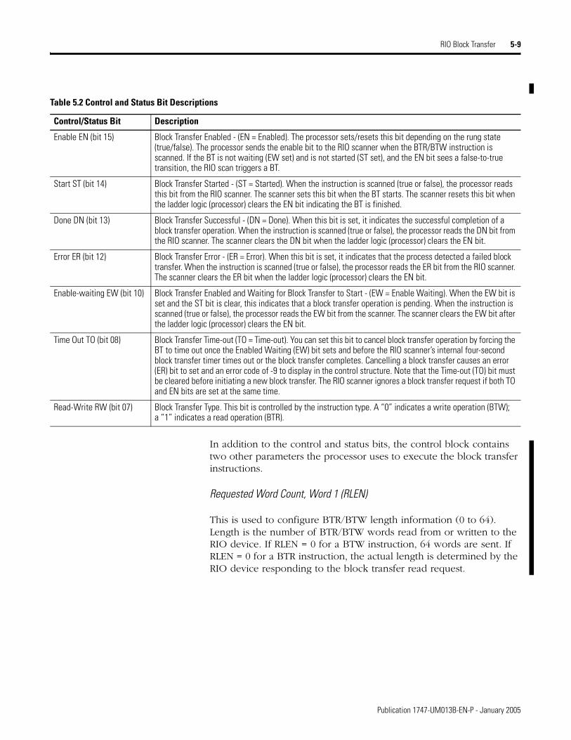
RIO Block Transfer 5-9
In addition to the control and status bits, the control block contains two other parameters the processor uses to execute the block transfer instructions.
Requested Word Count, Word 1 (RLEN)
This is used to configure BTR/BTW length information (0 to 64). Length is the number of BTR/BTW words read from or written to the RIO device. If RLEN = 0 for a BTW instruction, 64 words are sent. If RLEN = 0 for a BTR instruction, the actual length is determined by the RIO device responding to the block transfer read request.
Table 5.2 Control and Status Bit Descriptions
Control/Status Bit Description
Enable EN (bit 15) Block Transfer Enabled - (EN = Enabled). The processor sets/resets this bit depending on the rung state (true/false). The processor sends the enable bit to the RIO scanner when the BTR/BTW instruction is scanned. If the BT is not waiting (EW set) and is not started (ST set), and the EN bit sees a false-to-true transition, the RIO scan triggers a BT.
Start ST (bit 14) Block Transfer Started - (ST = Started). When the instruction is scanned (true or false), the processor reads this bit from the RIO scanner. The scanner sets this bit when the BT starts. The scanner resets this bit when the ladder logic (processor) clears the EN bit indicating the BT is finished.
Done DN (bit 13) Block Transfer Successful - (DN = Done). When this bit is set, it indicates the successful completion of a block transfer operation. When the instruction is scanned (true or false), the processor reads the DN bit from the RIO scanner. The scanner clears the DN bit when the ladder logic (processor) clears the EN bit.
Error ER (bit 12) Block Transfer Error - (ER = Error). When this bit is set, it indicates that the process detected a failed block transfer. When the instruction is scanned (true or false), the processor reads the ER bit from the RIO scanner. The scanner clears the ER bit when the ladder logic (processor) clears the EN bit.
Enable-waiting EW (bit 10) Block Transfer Enabled and Waiting for Block Transfer to Start - (EW = Enable Waiting). When the EW bit is set and the ST bit is clear, this indicates that a block transfer operation is pending. When the instruction is scanned (true or false), the processor reads the EW bit from the scanner. The scanner clears the EW bit after the ladder logic (processor) clears the EN bit.
Time Out TO (bit 08) Block Transfer Time-out (TO = Time-out). You can set this bit to cancel block transfer operation by forcing the BT to time out once the Enabled Waiting (EW) bit sets and before the RIO scanner’s internal four-second block transfer timer times out or the block transfer completes. Cancelling a block transfer causes an error (ER) bit to set and an error code of -9 to display in the control structure. Note that the Time-out (TO) bit must be cleared before initiating a new block transfer. The RIO scanner ignores a block transfer request if both TO and EN bits are set at the same time.
Read-Write RW (bit 07) Block Transfer Type. This bit is controlled by the instruction type. A “0” indicates a write operation (BTW); a “1” indicates a read operation (BTR).
Publication 1747-UM013B-EN-P - January 2005
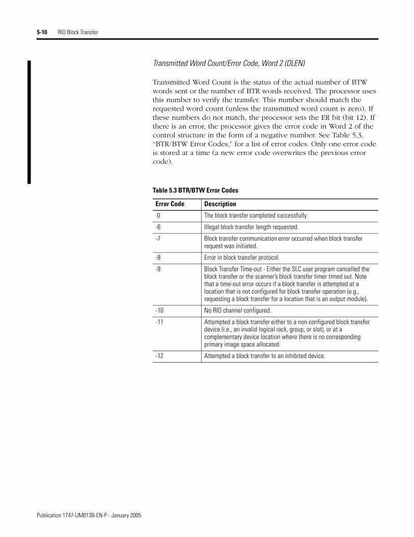
5-10 RIO Block Transfer
Transmitted Word Count/Error Code, Word 2 (DLEN)
Transmitted Word Count is the status of the actual number of BTW words sent or the number of BTR words received. The processor uses this number to verify the transfer. This number should match the requested word count (unless the transmitted word count is zero). If these numbers do not match, the processor sets the ER bit (bit 12). If there is an error, the processor gives the error code in Word 2 of the control structure in the form of a negative number. See Table 5.3, “BTR/BTW Error Codes,” for a list of error codes. Only one error code is stored at a time (a new error code overwrites the previous error code).
Table 5.3 BTR/BTW Error Codes
Error Code Description
0 The block transfer completed successfully.
-6 Illegal block transfer length requested.
-7 Block transfer communication error occurred when block transfer request was initiated.
-8 Error in block transfer protocol.
-9 Block Transfer Time-out - Either the SLC user program cancelled the block transfer or the scanner’s block transfer timer timed out. Note that a time-out error occurs if a block transfer is attempted at a location that is not configured for block transfer operation (e.g., requesting a block transfer for a location that is an output module).
-10 No RIO channel configured.
-11 Attempted a block transfer either to a non-configured block transfer device (i.e., an invalid logical rack, group, or slot), or at a complementary device location where there is no corresponding primary image space allocated.
-12 Attempted a block transfer to an inhibited device.
Publication 1747-UM013B-EN-P - January 2005

RIO Block Transfer 5-11
Instruction Operation
1. The scanner processes the BTR/BTW when it detects that the SLC control program rung, which contains the BTR/BTW, goes true.
If the RIO scanner detects any problem at this point (such as invalid block transfer control field, or unconfigured device), the control structure word 2 fills with the error code and the ER bit (bit 12) is set. If no problems occur, the EW bit (bit 10) and ST bit (bit 14) are set in the control block.
The SLC control program can monitor the block transfer by examining bits in word 0 of the control block. They indicate when the scanner has started processing (EW and ST) the block transfer and whether the block transfer operation completed successfully (DN) or failed (ER). The SLC control program can take different actions based on these status bits.
2. When a block transfer completes successfully, the DN bit is set. This indicates that the block transfer control block has been updated with the actual transmitted word count. This is important for BTR instructions, because this indicates the number of valid data words received from the remote device. This data is stored in the BTR data file.
3. If the block transfer fails, the length field and the data file are not updated. The ER bit is set and the error code field indicates the problem.
4. The SLC control program must indicate to the scanner when it is done processing the status word in the control structure (because DN or ER was set) so the corresponding control bits can be reused for another block transfer operation. The SLC control program indicates that it is done processing the block transfer when it solves the BT rung false, which clears the EN bit in the control block.
TIP The ST bit is not set if the scanner is already in the process of block transferring data to a location within the same logical RIO rack. The ST bit is set only after any previous pending block transfers to the same logical rack are completed and the block transfer request is scheduled on the RIO link.
Publication 1747-UM013B-EN-P - January 2005
5-12 RIO Block Transfer
5. When the RIO scanner detects that the EN bit cleared, it then clears the EW, ST and DN or ER bits, as well as the Transmitted Word Count/Error Code. This ensures that the status bits in the control block are not reflecting the results of the previous block transfer operation.
Programming Examples
IMPORTANT To prevent configuration conflicts, it is highly recommended that each M-file buffer (My:e.x00) should be used by only one block transfer instruction.
Table 5.4 Block Transfer Programming Examples
Figure 5.2, "Directional" on page 5-13
Figure 5.3, "Directional Repeating" on page 5-13
Figure 5.4, "Directional Continuous" on page 5-14
Figure 5.5, "Bi-directional Continuous" on page 5-14
Figure 5.6, "Bi-directional Alternating" on page 5-15
Figure 5.7, "Bi-directional Alternating Repeating" on page 5-15
Publication 1747-UM013B-EN-P - January 2005
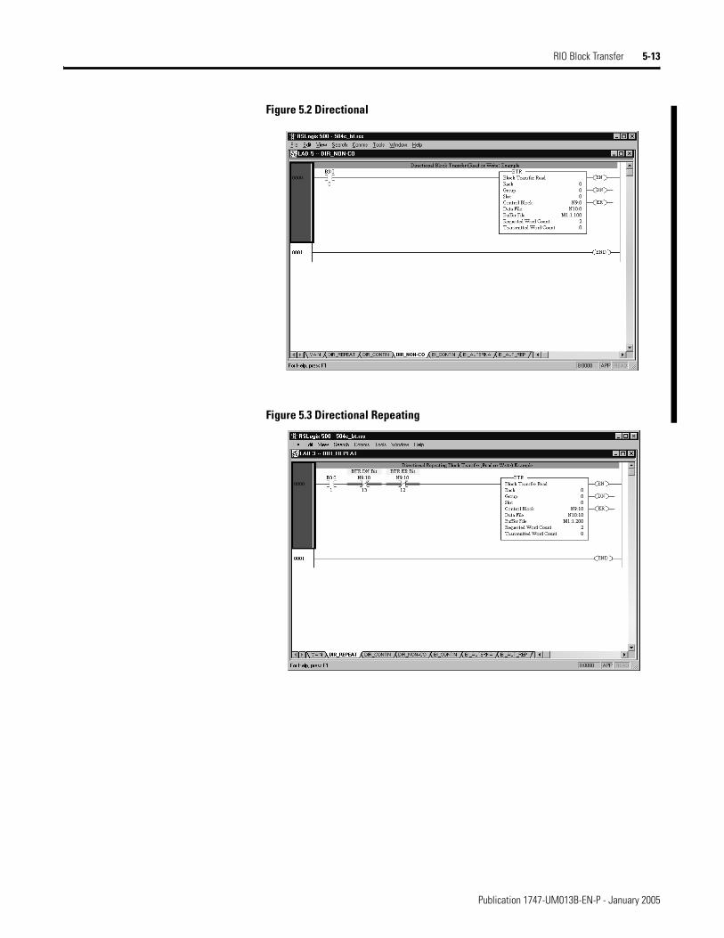
RIO Block Transfer 5-13
Figure 5.2 Directional
Figure 5.3 Directional Repeating
Publication 1747-UM013B-EN-P - January 2005

5-14 RIO Block Transfer
Figure 5.4 Directional Continuous
Figure 5.5 Bi-directional Continuous
Publication 1747-UM013B-EN-P - January 2005

RIO Block Transfer 5-15
Figure 5.6 Bi-directional Alternating
Figure 5.7 Bi-directional Alternating Repeating
Publication 1747-UM013B-EN-P - January 2005
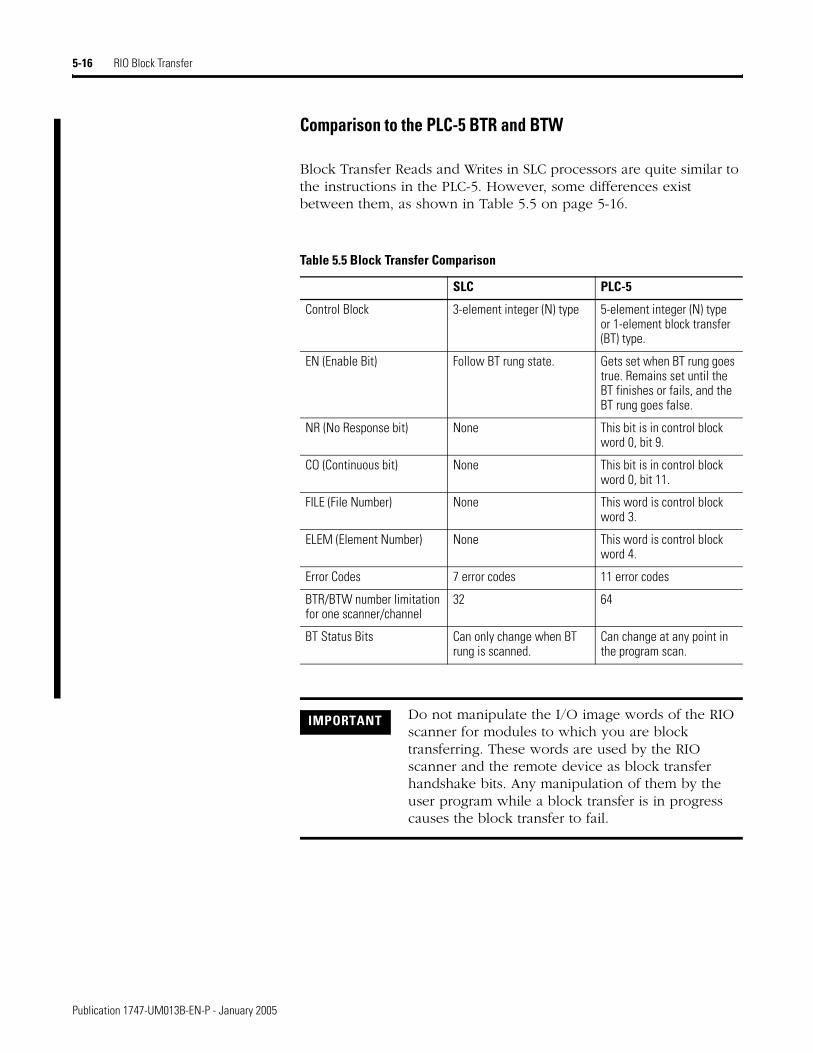
5-16 RIO Block Transfer
Comparison to the PLC-5 BTR and BTW
Block Transfer Reads and Writes in SLC processors are quite similar to the instructions in the PLC-5. However, some differences exist between them, as shown in Table 5.5 on page 5-16.
Table 5.5 Block Transfer Comparison
SLC PLC-5
Control Block 3-element integer (N) type 5-element integer (N) type or 1-element block transfer (BT) type.
EN (Enable Bit) Follow BT rung state. Gets set when BT rung goes true. Remains set until the BT finishes or fails, and the BT rung goes false.
NR (No Response bit) None This bit is in control block word 0, bit 9.
CO (Continuous bit) None This bit is in control block word 0, bit 11.
FILE (File Number) None This word is control block word 3.
ELEM (Element Number) None This word is control block word 4.
Error Codes 7 error codes 11 error codes
BTR/BTW number limitation for one scanner/channel
32 64
BT Status Bits Can only change when BT rung is scanned.
Can change at any point in the program scan.
IMPORTANT Do not manipulate the I/O image words of the RIO scanner for modules to which you are block transferring. These words are used by the RIO scanner and the remote device as block transfer handshake bits. Any manipulation of them by the user program while a block transfer is in progress causes the block transfer to fail.
Publication 1747-UM013B-EN-P - January 2005
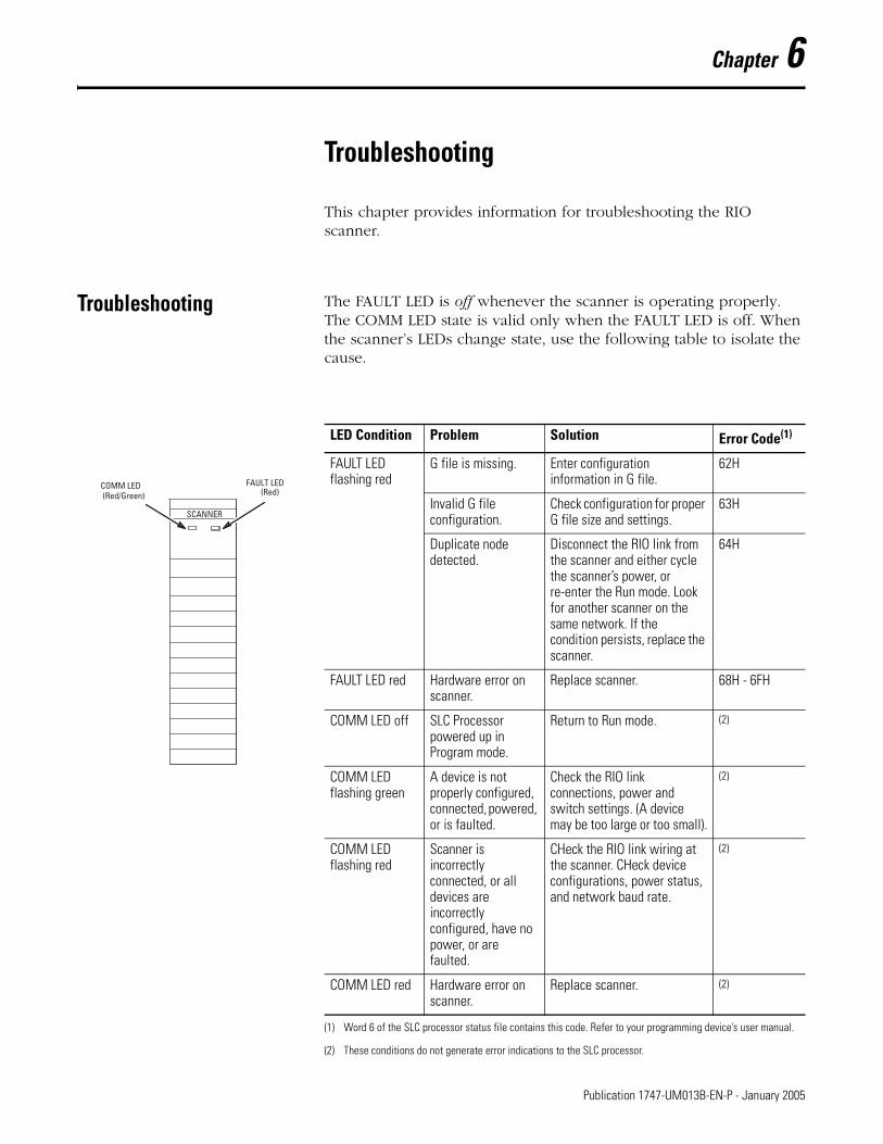
Chapter 6
Troubleshooting
This chapter provides information for troubleshooting the RIO scanner.
Troubleshooting The FAULT LED is off whenever the scanner is operating properly. The COMM LED state is valid only when the FAULT LED is off. When the scanner’s LEDs change state, use the following table to isolate the cause.
LED Condition Problem Solution Error Code(1)
(1) Word 6 of the SLC processor status file contains this code. Refer to your programming device’s user manual.
FAULT LED flashing red
G file is missing. Enter configuration information in G file.
62H
Invalid G file configuration.
Check configuration for proper G file size and settings.
63H
Duplicate node detected.
Disconnect the RIO link from the scanner and either cycle the scanner’s power, or re-enter the Run mode. Look for another scanner on the same network. If the condition persists, replace the scanner.
64H
FAULT LED red Hardware error on scanner.
Replace scanner. 68H - 6FH
COMM LED off SLC Processor powered up in Program mode.
Return to Run mode. (2)
(2) These conditions do not generate error indications to the SLC processor.
COMM LED flashing green
A device is not properly configured, connected, powered, or is faulted.
Check the RIO link connections, power and switch settings. (A device may be too large or too small).
(2)
COMM LED flashing red
Scanner is incorrectly connected, or all devices are incorrectly configured, have no power, or are faulted.
CHeck the RIO link wiring at the scanner. CHeck device configurations, power status, and network baud rate.
(2)
COMM LED red Hardware error on scanner.
Replace scanner. (2)
SCANNER
COMM LED(Red/Green) (Red)
FAULT LED
1 Publication 1747-UM013B-EN-P - January 2005

6-2 Troubleshooting
Error Codes The SLC processor reports error codes in word 6 of the SLC processor status file. Below are the format of the status word and applicable error codes.
For a complete description of the error codes, refer to the user manual provided with your programming device.
Retry Counters Electrically noisy environments can cause RIO communication problems. You can use the retry counters to determine if your scanner is having problems communicating with configured devices. To access retry counter information, you must view status file words M1:e.16 through M1:e.31 (and M1:e.32 through M1:e.47 if complementary I/O is used). These counters display the number of communication retries the scanner has made. See the section on retry counters in Chapter 4, Configuration and Programming for more detailed information.
Block Transfers If you are having problems with Block Transfers, see Chapter 5, RIO Block Transfer, for information on error codes.
Slot Number Error Code62H - G File is missing63H - Invalid user configuration64H - Duplicate node fault
01H to 1EH
68H to 6FH - Scanner hardware problem
Publication 1747-UM013B-EN-P - January 2005
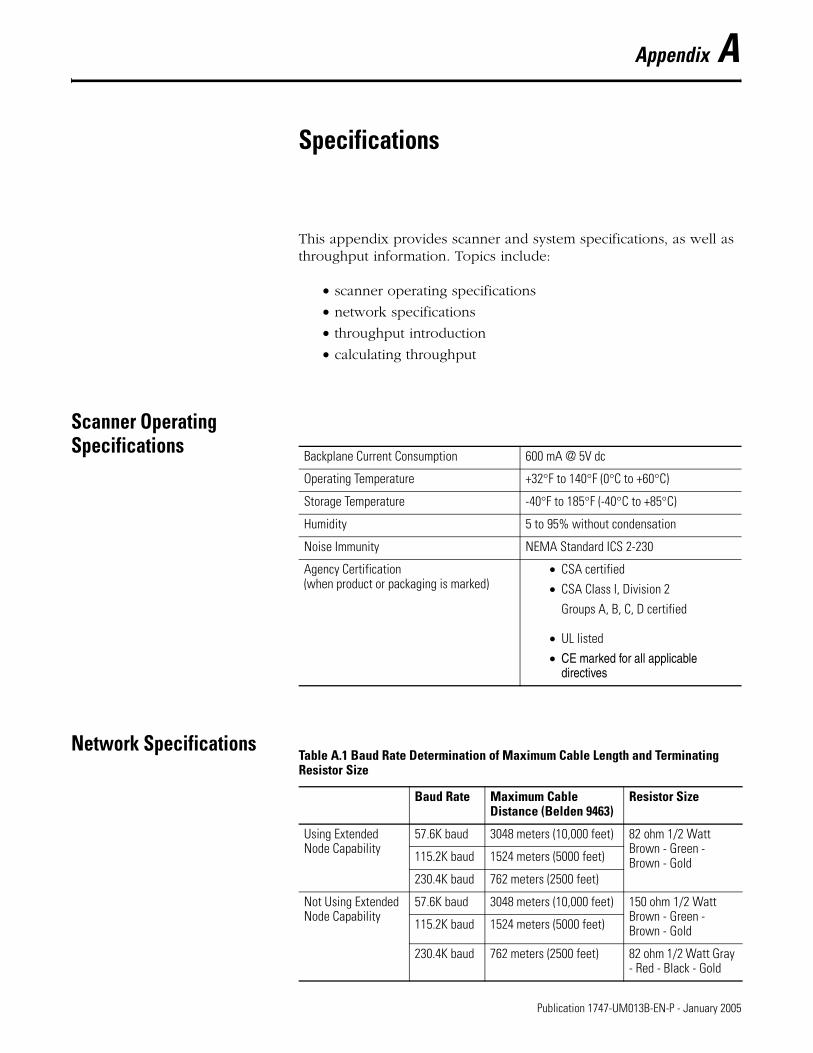
Appendix A
Specifications
This appendix provides scanner and system specifications, as well as throughput information. Topics include:
• scanner operating specifications
• network specifications
• throughput introduction
• calculating throughput
Scanner Operating Specifications
Network Specifications
Backplane Current Consumption 600 mA @ 5V dc
Operating Temperature +32°F to 140°F (0°C to +60°C)
Storage Temperature -40°F to 185°F (-40°C to +85°C)
Humidity 5 to 95% without condensation
Noise Immunity NEMA Standard ICS 2-230
Agency Certification(when product or packaging is marked)
• CSA certified
• CSA Class I, Division 2
Groups A, B, C, D certified
• UL listed
• CE marked for all applicable directives
Table A.1 Baud Rate Determination of Maximum Cable Length and Terminating Resistor Size
Baud Rate Maximum Cable Distance (Belden 9463)
Resistor Size
Using Extended Node Capability
57.6K baud 3048 meters (10,000 feet) 82 ohm 1/2 Watt Brown - Green - Brown - Gold115.2K baud 1524 meters (5000 feet)
230.4K baud 762 meters (2500 feet)
Not Using Extended Node Capability
57.6K baud 3048 meters (10,000 feet) 150 ohm 1/2 Watt Brown - Green - Brown - Gold115.2K baud 1524 meters (5000 feet)
230.4K baud 762 meters (2500 feet) 82 ohm 1/2 Watt Gray - Red - Black - Gold
1 Publication 1747-UM013B-EN-P - January 2005

A-2 Specifications
Throughput Introduction RIO throughput is defined as the time between when an input event occurs at an I/O module in an RIO chassis to when an output event occurs at an I/O module within the same RIO chassis. There are three types of throughput concerning the 1747-SN Series B Scanner and its RIO network:
• discrete throughput (time from discretely mapped input to discretely mapped output) without block transfers (BTs) present
• discrete throughput (time from discretely mapped input to discretely mapped output) with BTs present
• BT throughput (time from when a BT is enabled to when the BT successfully completes)
RIO Network Throughput Components
The following components affect RIO network throughput:
• the total SLC processor scan time
• the total RIO link scan time
• adapter(s) backplane scan time(s)
• the scanner’s output delay time
• the scanner’s input delay time
• input module delay times
• output module delay times
Table A.2 DIP Switch Position for Baud Rate Selection
Baud Rate DIP Switch Position
Switch 1 Switch 2
57.6K baud on on
115.2K baud on off
230.4K baud off on
230.4K baud off off
Publication 1747-UM013B-EN-P - January 2005

Specifications A-3
When the SLC control program detects that the remote input has been turned on (via the scanner output image), it activates the remote output device (via the scanner output image). Throughput is then defined as the time between when the remote input device is activated to when the remote output turns on.
Calculating Throughput The 1747-SN Series B Scanner’s throughput is determined by using the formulas provided in this section.
Discrete I/O Throughput without Block Transfers (Tdm-nbt) Present
The information in this section is used to calculate the discrete throughput of the 1747-SN Scanner if there are no BTs occurring on the RIO link to any chassis.
If BTs are present on the RIO link you must use the Discrete I/O Throughput with Block Transfers (Tdm-bt) Present section to
determine your throughput. See page B-6.
The formula to calculate the maximum scanner discrete I/O throughput without BTs present is:
Tdm-nbt = The maximum discrete throughput without BTs in milliseconds (ms)
Remote Expansion Chassis
SLC Local Chassis
Remote Chassis
ScannerProcessor I/O Module
Output Device
I/O Module
Input Device
Outputs from ModulesInputs to Modules
Outputs to Modules
Inputs from Modules
RIO Scan
ASB Module
ASB Backplane Scan
Processor ScanScanner Scan
Tdm nbt– 2Tps 2TRIO Tadp TSNo TSNi Tid Tod+ + + + + +=
Publication 1747-UM013B-EN-P - January 2005

A-4 Specifications
To calculate Tdm-nbt throughput, substitute values for the variables in
the formula above. Locate these values in the following documents:
RIO Scan Time Calculation (TRIO)
The RIO scan time is calculated by identifying the baud rate and image size of each logical device on the RIO link. Locate the corresponding time value in the following table. If you are using multiple logical devices, add the time values together to determine the total RIO scan time (TRIO).
Variable Variable Description Location of Variable
Tps The total processor scan time (ms)
Measured or estimated
TRIO The total RIO scan time (ms) see the section RIO Scan Time Calculation (TRIO) on page A-4
Tadp The adapter throughput delay. For a 1747-ASB, this is two ASB backplane scan times.
adapter user manual
TSNo The scanner module output delay time (ms)
see the section RIO Scanner Output Delay Time (TSNo) on page A-13
TSNi The scanner module input delay time (ms)
5 ms (constant value for all formulas in this appendix)
Tid The input module delay time (ms)
I/O product data and I/O instruction sheets
Tod The output module delay time (ms)
I/O product data and I/O instruction sheets
RIO Scan TImes for Adapters
Adapter Size Baud Rate
57.6K 115.2K 230.4K
1/4 logical rack 6.0 ms 3.5 ms 2.5 ms
1/2 logical rack 6.5 ms 4.0 ms 2.75 ms
3/4 logical rack 7.5 ms 4.5 ms 3.0 ms
Full logical rack 9.5 ms 5.5 ms 3.5 ms
TRIO Tadapter1 Tadapter2 Tadapter3+ +=
Publication 1747-UM013B-EN-P - January 2005

Specifications A-5
Example Discrete I/O Throughput without Block Transfers Present
An SLC 5/03 is controlling an RIO link running at 115.2K baud that has the following adapters:
• One 1747-ASB module is configured as a 1/2 logical rack starting at logical rack 0.I/O chassis slot 1 contains 1746-IB16, 16 point input moduleI/O chassis slot 2 contains 1746-OB16, 16 point output module
• Two adapters are each configured as full logical racks (logical racks 1 and 2).
• Three adapters are each configured as 1/4 logical racks (logical rack 3).
You need to calculate your Tdm-nbt: the RIO throughput time from
when the input closes on the 1746-IN16 until the output on the 1746-OB16 is on.
1. Use the throughput formula to calculate the maximum throughput.
Tps = 25.0 ms
TRIO = The total RIO scan time (ms)
TSNo = See value in the table on page A-14, TSNo without M0
File Writes (Normal Mode).
TSNi = 5.0 ms
Tid = 10.0 ms, which is from I/O module instruction sheets
Tod = 1.0 ms, which is from I/O module instruction sheets
Tdm-nbt = 2(25.0) + 2TRIO + 8.0 + TSNo + 5.0 + 10.0 + 1.0
2. Calculate the total RIO scan time (TRIO). Locate the baud rate
(115.2K) and adapter size, which is found in the table on page A-4. Multiply the RIO scan times listed under the 115.2K heading by the number of each different type of rack that you have. Add those numbers together:
Tdm nbt– 2Tps 2TRIO TADP TSNo TSNi Tid Tod+ + + + + +=
TRIO Tadapter1 Tadapter2 Tadapter3+ +=
Publication 1747-UM013B-EN-P - January 2005

A-6 Specifications
TRIO = 1(4.0 ms) + 2(5.5 ms) + 3(3.5 ms)
TRIO = 25.5 ms
3. Find TSNo on page A-14 in the table TSNo without M0 File
Writes (Normal Mode). For this example Tupd > Thold, and
there are 4 logical racks configured. Therefore:
TSNo = 7.0 ms
4. Substitute all the values for variables in the throughput formula and solve for throughput:
Tdm-nbt = 2(25.0)+ 2(25.5) + 8.0 + 7.0 + 5.0 + 10.0 + 1.0
Tdm-nbt = 132.0 ms = maximum throughput
Discrete I/O Throughput with Block Transfers (Tdm-bt) Present
The information in this section is used to calculate the discrete throughput of the 1747-SN Scanner if there are BTs occurring on the RIO link to any chassis.
If BTs are not present on the RIO link, you must use the Discrete I/O Throughput without Block Transfers (Tdm-nbt) Present section to
determine your throughput. See page A-3.
The formula to calculate discrete I/O throughput with BTs present is:
Tdm-bt = The maximum discrete throughput with BTs in
milliseconds (ms)
To calculate Tdm-bt throughput, substitute values for the variables in
the formula above. Locate these values in the following documents:
Tdm nbt– 2Tps 2TRIO 2Tbp TSNo TSNi Tid Tod+ + + + + +=
Tdm bt– 2Tps 2TRIO 2Tbtx Tadp TSNo bt– TSNi Tid T+ + + + + + +=od
Publication 1747-UM013B-EN-P - January 2005
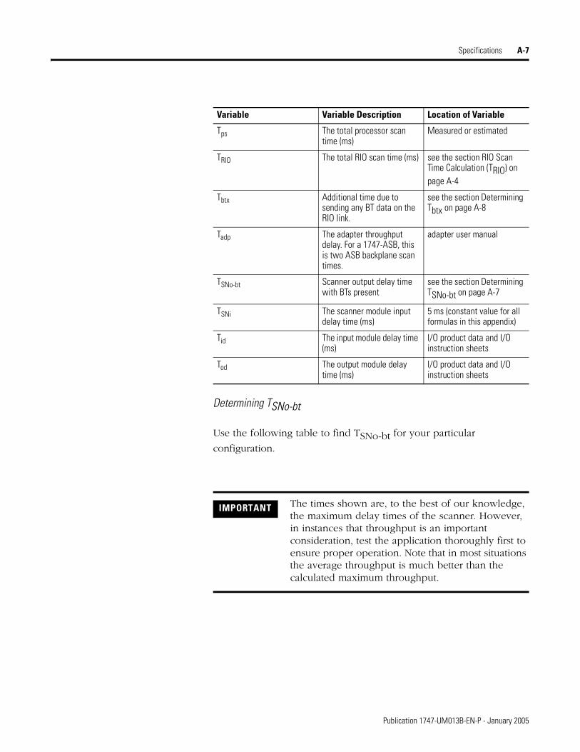
Specifications A-7
Determining TSNo-bt
Use the following table to find TSNo-bt for your particular
configuration.
Variable Variable Description Location of Variable
Tps The total processor scan time (ms)
Measured or estimated
TRIO The total RIO scan time (ms) see the section RIO Scan Time Calculation (TRIO) on page A-4
Tbtx Additional time due to sending any BT data on the RIO link.
see the section Determining Tbtx on page A-8
Tadp The adapter throughput delay. For a 1747-ASB, this is two ASB backplane scan times.
adapter user manual
TSNo-bt Scanner output delay time with BTs present
see the section Determining TSNo-bt on page A-7
TSNi The scanner module input delay time (ms)
5 ms (constant value for all formulas in this appendix)
Tid The input module delay time (ms)
I/O product data and I/O instruction sheets
Tod The output module delay time (ms)
I/O product data and I/O instruction sheets
IMPORTANT The times shown are, to the best of our knowledge, the maximum delay times of the scanner. However, in instances that throughput is an important consideration, test the application thoroughly first to ensure proper operation. Note that in most situations the average throughput is much better than the calculated maximum throughput.
Publication 1747-UM013B-EN-P - January 2005

A-8 Specifications
Determining Tbtx
Before determining (Tbtx), you need to establish the maximum BT
write or read length that is to be processed by each logical rack on the RIO link. RIO scan time is increased each time an BT is sent to any logical device on the RIO network. The scan time increase depends on the number of words sent in the BT and the selected baud rate.
RIO link protocol allows for a maximum of one BT to be sent to each logical rack on the RIO link during any single RIO scan. Therefore, if multiple BTs are sent to devices within the same logical rack, only the longest BT to that logical rack needs to be considered to determine your maximum throughput. The RIO scan time increase (Tri) for each
logical rack is:
The total increase in the RIO scan time (Tbtx) is equal to:
Tbtx = sum of Tri for all logical racks
Example Discrete I/O Throughput with Block Transfers Present
An SLC 5/03 is using a scanner to control a 115.2K baud RIO link that has 3 adapters and 4 logical devices.
Number of Logical Racks Configured(1)
(1) See page A-12 if you are not sure how to determine the number of logical racks configured.
Normal Mode Complementary Mode
All Baud Rates
57.6K baud 115.2K baud 230.4K baud
1 Logical Rack 16.0 19.0 24.0 32.0
2 Logical Racks 19.0 23.0 27.0 36.0
3 Logical Racks 22.0 26.0 30.0 39.0
4 Logical Racks 25.0 28.0 34.0 42.0
Baud Rate RIO Scan Time Increase (Tri)
57.6K baud 0.300 x BT length + 5.0 ms
115.2K baud 0.150 x BT length + 3.5 ms
230.4K baud 0.075 x BT length +2.0 ms
Publication 1747-UM013B-EN-P - January 2005

Specifications A-9
Adapter #1 (1747-ASB module):
• starting logical rack 0, logical group 0
• 12 logical groups (1 1/2 logical racks)
• one 8 word and two 4 word BT write/read modules in logical rack 0
• one 2 word BT write/read module in logical rack 1
Adapter #2 (1771-ASB module):
• starting logical rack 2, logical group 0
• 2 logical groups (1/4 logical rack)
• one 64 word BT write/read module
Adapter #3 (1771-ASB module):
• starting logical rack 2, logical group 2
• 2 logical groups (1/4 logical rack)
• one 32 word BT write/read module
1. Use the throughput formula to calculate the maximum throughput of the 1747-ASB module.
Tdm-bt = 2Tps + 2TRIO + 2Tbtx + Tadp + TSNo-bt + TSNi + Tid
+ Tod
Tps = 25.0 ms
TRIO = The total RIO scan time (ms)
Tbtx = Additional time due to sending any BT data on the RIO
link
Tadp = Two 1747-ASB module backplane scan times (calculated
from ASB manual) = 2(4.5) = 9.0 ms
TSNo-bt = 22.0 ms from the table on page A-14, TSNo with
Block Transfers (Normal Mode). There are 3 logical racks configured.
TSNi = 5.0 ms
Tid = 10.0 ms, which is from I/O module instruction sheets
Tod = 1.0 ms, which is from I/O module instruction sheets
Publication 1747-UM013B-EN-P - January 2005

A-10 Specifications
Tdm-bt = 2(25.0) + 2TRIO + 2Tbtx + 9.0 + 22.0 + 5.0 + 10.0 + 1.0
2. Calculate the total RIO scan time (TRIO). Locate the baud rate
(115.2K) and adapter size which is found in the table on page B-4. Multiply the RIO scan times listed under the 115.2K heading by the number of each different type of rack that you have. Add those number together.
TRIO = Tadapter1 + Tadapter2 + Tadapter3
TRIO = 1(5.5) + 1(4.0) + 2(3.5)
TRIO = 16.5 ms
3. Calculate the maximum Tri time for each logical rack. Do this by
determining the largest BT that will occur to any device within a logical rack and calculating the transfer time using the table on page B-7. Then add together the Tri times for each logical rack
to obtain Tbtx.
Tri for rack 0 = 0.150(8) + 3.5 = 4.7 ms (maximum BT to rack 0
is 8 words)
Tri for rack 1 = 0.150(2) + 3.5 = 3.8 ms (maximum BT to rack 1
is 2 words)
Tri for rack 2 = 0.150(64) + 3.5 = 13.1 ms (maximum BT to rack
2 is 64 words)
Tbtx = Tri0 + Tri1 + Tri2 = 4.7 + 3.8 + 13.1 = 21.6 ms
4. Substitute all the values for variables in the throughput formula and solve for throughput.
Tdm-bt = 2(25.0) + 2(16.5) + 2(21.6) + 9.0 + 22.0 + 5.0 + 10.0 +
1.0
Tdm-bt = 173.2 ms = maximum throughput
Block Transfer Throughput
Block transfer throughput is the time from when the BT is enabled via the EN bit, until the DN bit is processed. The following BT timing explanations are based on the directional continuous BT example
Publication 1747-UM013B-EN-P - January 2005

Specifications A-11
shown on page, where a BT is retriggered automatically upon each completion.
BT throughput is always slower than discrete data transfer. Completing a BT is dependent on the time involved for the:
• SLC control program to enable the BT via an M0 file write(1)
• scanner to detect that a BT has been requested(2)
• BT to be waiting in the queue due to another BT already being
processed on the same logical rack(3)
• scanner to schedule a pending bit(2)
• adapter to acknowledge the request(4)
• scanner to initiate the BT and transfer the data(2)
• SLC control program to detect that the BT has completed (DN
flag set)(1)
The time to free up the BT buffer (by clearing the EN flag so another BT can be performed) depends on the:
• instruction time of the M0 file write which clears the EN flag(1)
• time for the scanner to detect that the EN flag has been
cleared(2)
• time for SLC control program to detect that the DN flag has been
cleared(1)
The formula to calculate BT throughput is:
The equation for freeing up the BT buffer is:
Substitute values for the variables in the formulas above. Locate these values in the following documents:
(1) This is dependent on the SLC processor you are using.
(2) Refer to the equations that follow.
(3) The RIO network allows only one BT per logical rack (not logical device) per RIO scan. Therefore, if multiple BTs are performed on devices within the same logical rack, BTs will have to wait in the queue until any previously scheduled BTs for the same logical rack have been completed.
(4) This is dependent on the RIO adapter.
TM0 TSN0 bt– number of BTs +1( ) Tbtwait 2TRIO 2Tbtx Tadp bt– Tps+ + + + + +
TM0 TSNo bt– Number of BTs( ) Tps+ +
Publication 1747-UM013B-EN-P - January 2005
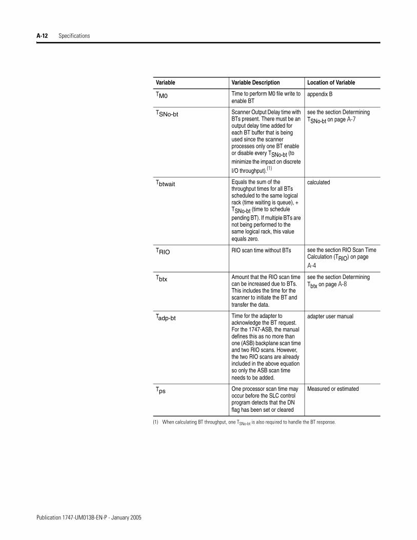
A-12 Specifications
Variable Variable Description Location of Variable
TM0 Time to perform M0 file write to enable BT
appendix B
TSNo-bt Scanner Output Delay time with BTs present. There must be an output delay time added for each BT buffer that is being used since the scanner processes only one BT enable or disable every TSNo-bt (to minimize the impact on discrete
I/O throughput).(1)
(1) When calculating BT throughput, one TSNo-bt is also required to handle the BT response.
see the section Determining TSNo-bt on page A-7
Tbtwait Equals the sum of the throughput times for all BTs scheduled to the same logical rack (time waiting is queue), + TSNo-bt (time to schedule pending BT). If multiple BTs are not being performed to the same logical rack, this value equals zero.
calculated
TRIO RIO scan time without BTs see the section RIO Scan Time Calculation (TRIO) on page
A-4
Tbtx Amount that the RIO scan time can be increased due to BTs. This includes the time for the scanner to initiate the BT and transfer the data.
see the section Determining Tbtx on page A-8
Tadp-bt Time for the adapter to acknowledge the BT request. For the 1747-ASB, the manual defines this as no more than one (ASB) backplane scan time and two RIO scans. However, the two RIO scans are already included in the above equation so only the ASB scan time needs to be added.
adapter user manual
Tps One processor scan time may occur before the SLC control program detects that the DN flag has been set or cleared
Measured or estimated
Publication 1747-UM013B-EN-P - January 2005
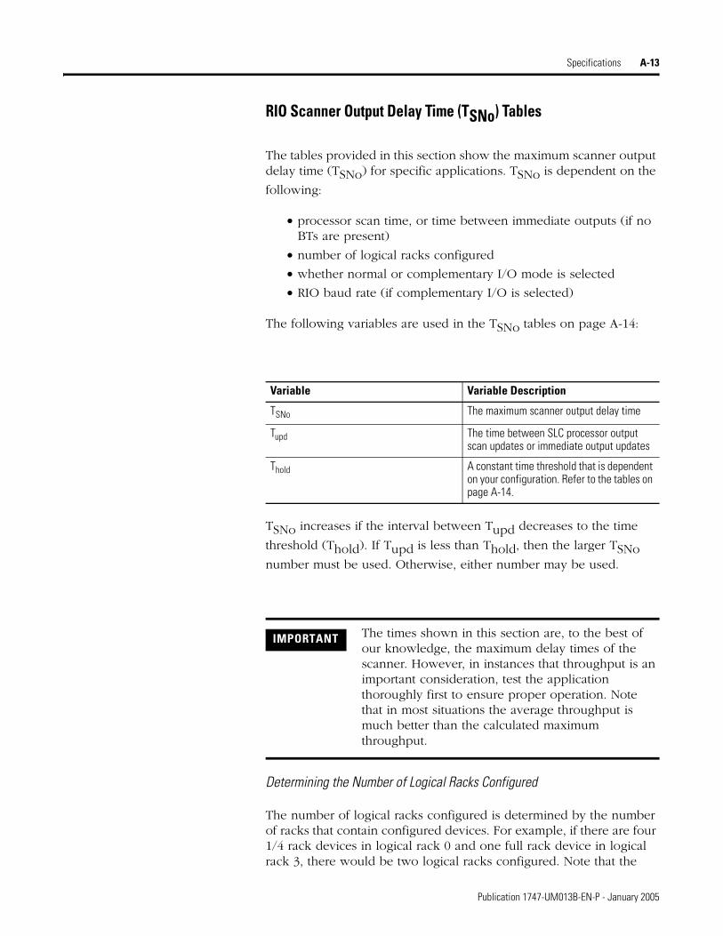
Specifications A-13
RIO Scanner Output Delay Time (TSNo) Tables
The tables provided in this section show the maximum scanner output delay time (TSNo) for specific applications. TSNo is dependent on the
following:
• processor scan time, or time between immediate outputs (if no BTs are present)
• number of logical racks configured
• whether normal or complementary I/O mode is selected
• RIO baud rate (if complementary I/O is selected)
The following variables are used in the TSNo tables on page A-14:
TSNo increases if the interval between Tupd decreases to the time
threshold (Thold). If Tupd is less than Thold, then the larger TSNo
number must be used. Otherwise, either number may be used.
Determining the Number of Logical Racks Configured
The number of logical racks configured is determined by the number of racks that contain configured devices. For example, if there are four 1/4 rack devices in logical rack 0 and one full rack device in logical rack 3, there would be two logical racks configured. Note that the
Variable Variable Description
TSNo The maximum scanner output delay time
Tupd The time between SLC processor output scan updates or immediate output updates
Thold A constant time threshold that is dependent on your configuration. Refer to the tables on page A-14.
IMPORTANT The times shown in this section are, to the best of our knowledge, the maximum delay times of the scanner. However, in instances that throughput is an important consideration, test the application thoroughly first to ensure proper operation. Note that in most situations the average throughput is much better than the calculated maximum throughput.
Publication 1747-UM013B-EN-P - January 2005

A-14 Specifications
number of logical devices on the RIO network affects only TRIO, and
only affects TSNo when additional logical racks are used.
When complementary mode is selected, the number of configured racks is also determined by the number of primary or complementary racks configured, but not by both. (The maximum number of configured racksis 4.) That is, if there is a primary rack configured with a corresponding complementary rack, that is considered one logical rack. If there is a primary rack configured without a complementary rack (or vice versa), that also is considered one logical rack.
TSNo without M0 File Writes
Normal Mode(1)
(1) All times shown are in milliseconds (ms).
Number of Logical Racks Configured
All Baud Rates
TSNo if Tupd ≤ Thold Thold TSNo if Tupd>Thold
1 Logical Rack 5.0 5.0 2.5
2 Logical Rack 7.0 7.0 4.0
3 Logical Rack 9.0 9.0 5.5
4 Logical Rack 11.0 11.0 7.0
Complementary(1) (2)
Number of Logical Racks Configured
57.6K baud 115.2K baud 230.4K baud
TSNo if Tupd ≤ Thold
Thold TSNo if Tupd>Thold
TSNo if Tupd ≤ Thold
Thold TSNo if Tupd>Thold
TSNo if Tupd ≤ Thold
Thold TSNo if Tupd>Thold
1 Logical Rack 6.0 5.0 4.0 7.0 7.0 4.0 10.0 9.0 4.0
2 Logical Rack 9.0 8.0 5.0 10.0 10.0 6.0 12.0 12.0 7.0
3 Logical Rack 12.0 11.0 7.0 12.0 12.0 8.0 16.0 16.0 10.0
4 Logical Rack 15.0 14.0 9.0 16.0 16.0 10.0 21.0 22.0 13.0
(1) All times shown are in milliseconds (ms).
(2) Although a faster baud rate decreases RIO scan time (TRIO), it has an inverse affect on TSNo when complementary I/O mode is selected.
Publication 1747-UM013B-EN-P - January 2005

Specifications A-15
TSNo with M0 File Writes (No Block Transfers)
Normal Mode(1)
(1) All times shown are in milliseconds (ms).
Number of Logical Racks Configured
All Baud Rates
TSNo if Tupd ≤ Thold Thold TSNo if Tupd>Thold
1 Logical Rack 8.0 6.0 4.5
2 Logical Rack 10.0 8.0 5.5
3 Logical Rack 12.0 10.0 7.0
4 Logical Rack 14.0 12.0 8.0
Complementary(1) (2)
Number of Logical Racks Configured
57.6K baud 115.2K baud 230.4K baud
TSNo if Tupd ≤ Thold
Thold TSNo if Tupd>Thold
TSNo if Tupd ≤ Thold
Thold TSNo if Tupd>Thold
TSNo if Tupd ≤ Thold
Thold TSNo if Tupd>Thold
1 Logical Rack 10.0 6.0 6.0 12.0 8.0 8.0 15.0 10.0 9.0
2 Logical Rack 12.0 9.0 8.0 14.0 11.0 9.0 17.0 15.0 12.0
3 Logical Rack 15.0 12.0 9.0 16.0 14.0 11.0 21.0 20.0 14.0
4 Logical Rack 18.0 15.0 10.0 20.0 17.0 12.0 26.0 24.0 17.0
(1) All times shown are in milliseconds (ms).
(2) Although a faster baud rate decreases RIO scan time (TRIO), it has an inverse affect on TSNo when complementary I/O mode is selected.
Publication 1747-UM013B-EN-P - January 2005

A-16 Specifications
Publication 1747-UM013B-EN-P - January 2005

Appendix B
M0 - M1 Files and G Files
This appendix contains important information about M0-M1 files and G files. The information is general in nature and supplements specific information contained in earlier chapters of this manual.
M0 - M1 Files M0 and M1 files are data files that reside in specialty I/O modules only. There is no image for these files in the processor memory. The application of these files depends on the function of the particular specialty I/O module. With respect to the SLC processor (SLC 5/02 or later), the M0 file is a module output file (a write only file) and the M1 file is a module input file (a read only file). The opposite is true for specialty I/O modules, where the M0 file is a read only file, and the M1 file is a write only file.
M0 and M1 files can be addressed in your ladder program and they can also be acted upon by the specialty I/O module - independent of the processor scan. It is important that you keep the following in mind in creating and applying your ladder logic:
IMPORTANT During the processor scan, the ladder program can address M0 and M1 data with bit, word, or file instructions. Each time an M0-M1 file address is encountered in the program, an immediate data transfer to or from the specialty I/O module occurs. The impact these immediate data transfers have on processor scan time is described in Appendix D of the SLC 500 Instruction Set Reference Manual, Publication 1747-RM001.
1 Publication 1747-UM013B-EN-P - January 2005
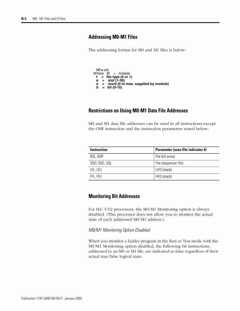
B-2 M0 - M1 Files and G Files
Addressing M0-M1 Files
The addressing format for M0 and M1 files is below:
Restrictions on Using M0-M1 Data File Addresses
M0 and M1 data file addresses can be used in all instructions except the OSR instruction and the instruction parameters noted below:
Monitoring Bit Addresses
For SLC 5/02 processors, the M0/M1 Monitoring option is always disabled. (This processor does not allow you to monitor the actual state of each addressed M0/M1 address.)
M0/M1 Monitoring Option Disabled
When you monitor a ladder program in the Run or Test mode with the M0/M1 Monitoring option disabled, the following bit instructions, addressed to an M0 or M1 file, are indicated as false regardless of their actual true/false logical state.
Instruction Parameter (uses file indicator #)
BSL, BSR File (bit array)
SQO, SQC, SQL File (sequencer file)
LFL, LFU LIFO (stack)
FFL, FFU FIFO (stack)
Mf:e.s/bWhere M = module f = file type (0 or 1) e = slot (1-30) s = word (0 to max. supplied by module) b = bit (0-15)
Publication 1747-UM013B-EN-P - January 2005

M0 - M1 Files and G Files B-3
If you need to show the state of the M0 or M1 addressed bit, you can transfer the state to an internal processor bit. This is illustrated below, where an internal processor bit is used to indicate the true/false state of a rung.
M0/M1 Monitoring Option Enabled
The SLC 5/03, SLC 5/04 and SLC 5/05 processors allows you to monitor the actual state of each addressed M0/M1 address (or data table). The highlighting appears normal when compared to the other processor data files. The processor’s performance will be degraded to the degree of M0/M1 referenced screen data. For example, if your screen has only one M0/M1 element, degradation will be minimal. If your screen has 69 M0/M1 elements, degradation will be significant.
When you are monitoring the ladder program in the Run or Test mode, the APS or HHT display does not show these instructions as being true when the processor evaluates them as true.
] [Mf:e.s
b]/[
Mf:e.s
b( )
Mf:e.s
b(L)
Mf:e.s
b(U)
Mf:e.s
b
f = file (0 or 1)
When you are monitoring the ladder program in the Run or Test mode, the display does not show these instructions as being true when the processor evaluates them as true.
This rung will not show its true rung state because the EQU instruction is always shown as true and the M0 instruction is always shown as false.
OTE instruction B3/2 has been added to the rung. This instruction shows the true or false state of the rung.
EQUEQUALSource A N7:12Source B N7:3
] [B3
0] [
B3
1( )
M0:3.0
1
( )M0:3.0
1
] [B3
0] [
B3
1
EQUEQUALSource A N7:12Source B N7:3
( )B3
2
IMPORTANT This option is not supported by the SLC 5/02 processor.
Publication 1747-UM013B-EN-P - January 2005

B-4 M0 - M1 Files and G Files
Transferring Data Between Processor Files and M0 or M1 Files
The processor does not contain an image of the M0 or M1 file. As a result, you must edit and monitor M0 and M1 file data via instructions in your ladder program. For example, you can copy a block of data from a processor data file to an M0 or M1 data file or vice versa using the COP instruction in your ladder program.
The COP instructions below copy data from a processor bit file and integer file to an M0 file. For the example, assume the data is configuration information affecting the operation of the specialty I/O module.
The COP instruction below copies data from an M1 data file to an integer file. This technique is used to monitor the contents of an M0 or M1 data file indirectly, in a processor data file.
Access Time
During the program scan, the processor must access the specialty I/O card to read/write M0 or M1 data. This access time must be added to the execution time of each instruction referencing M0 or M1 data. For the SLC 5/03, SLC 5/04 and SLC 5/05 processors, the instruction types vary in their execution times.
The following table shows approximate access times per instruction or word of data for the SLC 5/02, SLC 5/03, SLC 5/04 and SLC 5/05 processors.
COPCOPY FILESource #B3:0Dest #M0:1.0Length 16
COPCOPY FILESource #N7:0Dest #M0:1.16Length 27
] [S:1
15
First scan bit. It makes this rung true only for
the first scan afterentering Run mode.
COPCOPY FILESource #M1:4.3Dest #N10:0Length 6
Publication 1747-UM013B-EN-P - January 2005
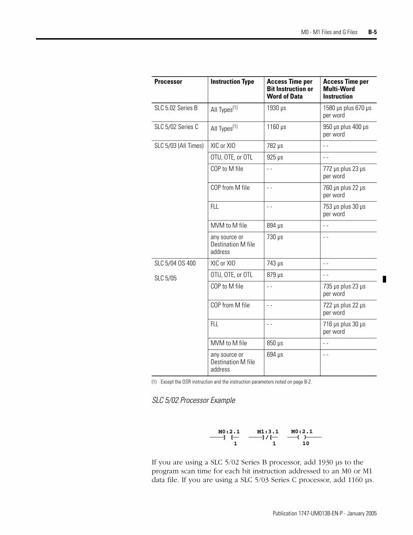
M0 - M1 Files and G Files B-5
SLC 5/02 Processor Example
If you are using a SLC 5/02 Series B processor, add 1930 µs to the program scan time for each bit instruction addressed to an M0 or M1 data file. If you are using a SLC 5/03 Series C processor, add 1160 µs.
Processor Instruction Type Access Time per Bit Instruction or Word of Data
Access Time perMulti-Word Instruction
SLC 5.02 Series B All Types(1)
(1) Except the OSR instruction and the instruction parameters noted on page B-2.
1930 µs 1580 µs plus 670 µs per word
SLC 5/02 Series C All Types(1) 1160 µs 950 µs plus 400 µs per word
SLC 5/03 (All Times) XIC or XIO 782 µs - -
OTU, OTE, or OTL 925 µs - -
COP to M file - - 772 µs plus 23 µs per word
COP from M file - - 760 µs plus 22 µs per word
FLL - - 753 µs plus 30 µs per word
MVM to M file 894 µs - -
any source or Destination M file address
730 µs - -
SLC 5/04 OS 400
SLC 5/05
XIC or XIO 743 µs - -
OTU, OTE, or OTL 879 µs - -
COP to M file - - 735 µs plus 23 µs per word
COP from M file - - 722 µs plus 22 µs per word
FLL - - 716 µs plus 30 µs per word
MVM to M file 850 µs - -
any source or Destination M file address
694 µs - -
] [M0:2.1
1]/[
M1:3.1
1( )
M0:2.1
10
Publication 1747-UM013B-EN-P - January 2005

B-6 M0 - M1 Files and G Files
If you are using a SLC 5/02 Series B processor, add 1580 µs plus 670 µs per word of data addressed to the M0 or M1 file. As shown above, 34 words are copied from #B3:0 to M0:1.0. Therefore, this adds 24360 µs to the scan time of the COP instruction. If you are using a SLC 5/02 Series C processor, add 950 µs plus 400 µs per word. This adds 14550 µs to the scan time of the COP instruction.
SLC 5/03 Processor Example
The SLC 5/03 processor access times depend on the instruction type. Consult the table on B-4 for the correct access times to add. As an example, if you use a COP to M file instruction like the one shown above, add 772 µs plus 23 µs per word. This adds 1554 µs to the SLC 5/03 processor scan time due to the COP instruction.
SLC 5/04 and SLC 5/05 Processor Example
The SLC 5/04 and SLC 5/05 processors access times depend on the instruction type. Consult the table on B-4 for the correct access times to add. As an example, if you use a COP to M file instruction like the one shown above, add 735 µs plus 23 µs per word. This adds 1517 µs to the processor scan time due to the COP instruction.
COPCOPY FILESource #B3:0Dest #M0:1.0Length 34
COPCOPY FILESource #B3:0Dest #M0:1.0Length 34
COPCOPY FILESource #B3:0Dest #M0:1.0Length 34
Publication 1747-UM013B-EN-P - January 2005
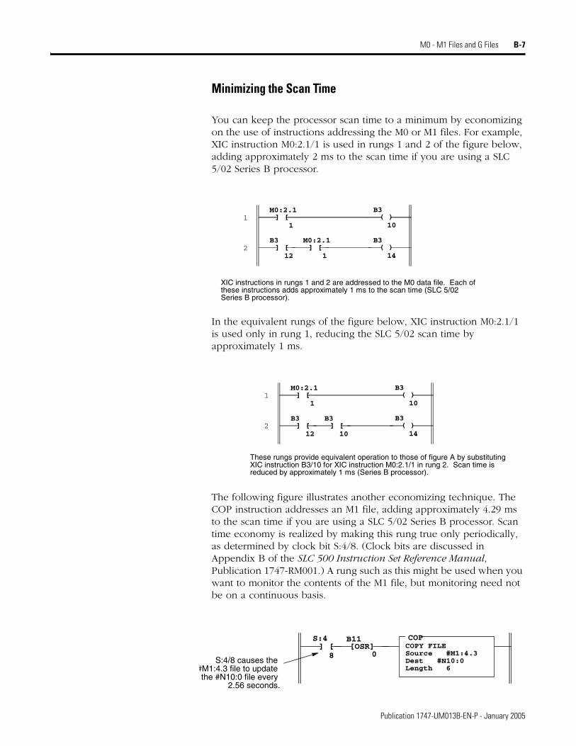
M0 - M1 Files and G Files B-7
Minimizing the Scan Time
You can keep the processor scan time to a minimum by economizing on the use of instructions addressing the M0 or M1 files. For example, XIC instruction M0:2.1/1 is used in rungs 1 and 2 of the figure below, adding approximately 2 ms to the scan time if you are using a SLC 5/02 Series B processor.
In the equivalent rungs of the figure below, XIC instruction M0:2.1/1 is used only in rung 1, reducing the SLC 5/02 scan time by approximately 1 ms.
The following figure illustrates another economizing technique. The COP instruction addresses an M1 file, adding approximately 4.29 ms to the scan time if you are using a SLC 5/02 Series B processor. Scan time economy is realized by making this rung true only periodically, as determined by clock bit S:4/8. (Clock bits are discussed in Appendix B of the SLC 500 Instruction Set Reference Manual, Publication 1747-RM001.) A rung such as this might be used when you want to monitor the contents of the M1 file, but monitoring need not be on a continuous basis.
XIC instructions in rungs 1 and 2 are addressed to the M0 data file. Each of these instructions adds approximately 1 ms to the scan time (SLC 5/02 Series B processor).
1
] [B3
12] [
M0:2.1
1( )
B3
14
] [M0:2.1
1( )
B3
10
2
These rungs provide equivalent operation to those of figure A by substitutingXIC instruction B3/10 for XIC instruction M0:2.1/1 in rung 2. Scan time is reduced by approximately 1 ms (Series B processor).
] [B3
12] [
B3
10( )
B3
14
] [M0:2.1
1( )
B3
101
2
[OSR]B11
0
COPCOPY FILESource #M1:4.3Dest #N10:0Length 6
] [S:4
8S:4/8 causes the
#M1:4.3 file to update the #N10:0 file every
2.56 seconds.
Publication 1747-UM013B-EN-P - January 2005
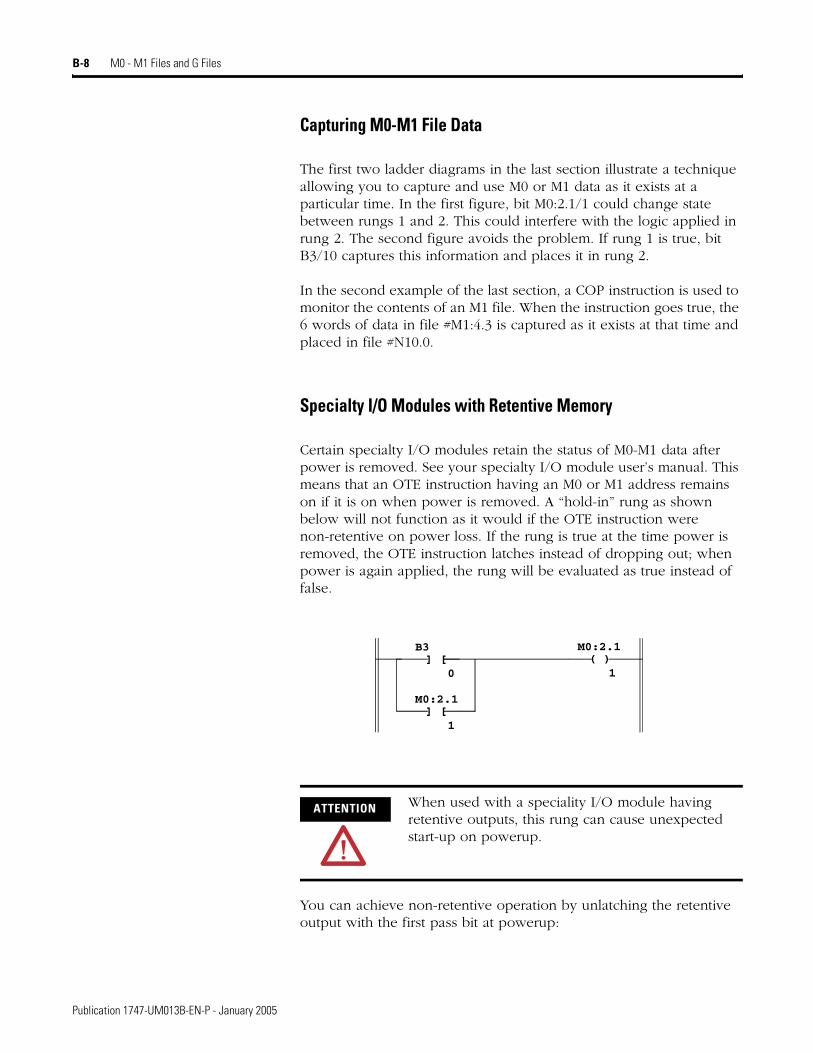
B-8 M0 - M1 Files and G Files
Capturing M0-M1 File Data
The first two ladder diagrams in the last section illustrate a technique allowing you to capture and use M0 or M1 data as it exists at a particular time. In the first figure, bit M0:2.1/1 could change state between rungs 1 and 2. This could interfere with the logic applied in rung 2. The second figure avoids the problem. If rung 1 is true, bit B3/10 captures this information and places it in rung 2.
In the second example of the last section, a COP instruction is used to monitor the contents of an M1 file. When the instruction goes true, the 6 words of data in file #M1:4.3 is captured as it exists at that time and placed in file #N10.0.
Specialty I/O Modules with Retentive Memory
Certain specialty I/O modules retain the status of M0-M1 data after power is removed. See your specialty I/O module user’s manual. This means that an OTE instruction having an M0 or M1 address remains on if it is on when power is removed. A “hold-in” rung as shown below will not function as it would if the OTE instruction were non-retentive on power loss. If the rung is true at the time power is removed, the OTE instruction latches instead of dropping out; when power is again applied, the rung will be evaluated as true instead of false.
You can achieve non-retentive operation by unlatching the retentive output with the first pass bit at powerup:
] [B3
0( )
M0:2.1
1
] [M0:2.1
1
ATTENTION When used with a speciality I/O module having retentive outputs, this rung can cause unexpected start-up on powerup.
Publication 1747-UM013B-EN-P - January 2005
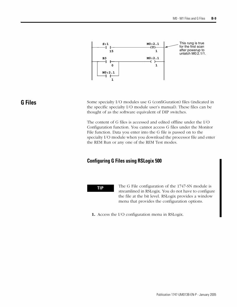
M0 - M1 Files and G Files B-9
G Files Some specialty I/O modules use G (confiGuration) files (indicated in the specific specialty I/O module user’s manual). These files can be thought of as the software equivalent of DIP switches.
The content of G files is accessed and edited offline under the I/O Configuration function. You cannot access G files under the Monitor File function. Data you enter into the G file is passed on to the specialty I/O module when you download the processor file and enter the REM Run or any one of the REM Test modes.
Configuring G Files using RSLogix 500
1. Access the I/O configuration menu in RSLogix.
] [S:1
15(U)
M0:2.1
1
] [B3
0( )
M0:2.1
1
] [M0:2.1
1
This rung is true for the first scan after powerup to unlatch M0:2.1/1.
TIP The G File configuration of the 1747-SN module is streamlined in RSLogix. You do not have to configure the file at the bit level. RSLogix provides a window menu that provides the configuration options.
Publication 1747-UM013B-EN-P - January 2005

B-10 M0 - M1 Files and G Files
Figure B.1 I/O Configuration Screen
2. Click the “Adv Config” button to access the next menu.
You can edit the number of words in each category. Although, it is recommended to leave them at default values unless specific project considerations require changes. See Chapter 4 for more information on configuring the module.
Figure B.2 Advanced Configuration Menu
Publication 1747-UM013B-EN-P - January 2005
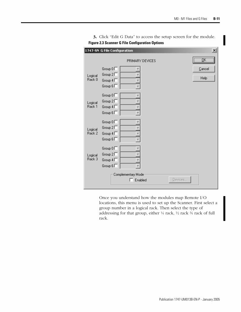
M0 - M1 Files and G Files B-11
3. Click “Edit G Data” to access the setup screen for the module.
Figure 2.3 Scanner G File Configuration Options
Once you understand how the modules map Remote I/O locations, this menu is used to set up the Scanner. First select a group number in a logical rack. Then select the type of addressing for that group, either ¼ rack, ½ rack ¾ rack of full rack.
Publication 1747-UM013B-EN-P - January 2005

B-12 M0 - M1 Files and G Files
Figure 2.4 Rack Configurations
Once you select the group and type of addressing, the I/O word layout for the group is shown.
Publication 1747-UM013B-EN-P - January 2005
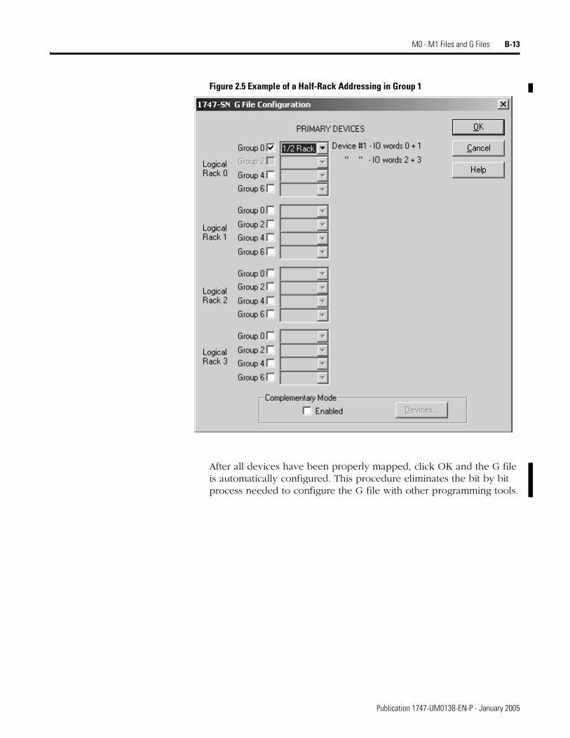
M0 - M1 Files and G Files B-13
Figure 2.5 Example of a Half-Rack Addressing in Group 1
After all devices have been properly mapped, click OK and the G file is automatically configured. This procedure eliminates the bit by bit process needed to configure the G file with other programming tools.
Publication 1747-UM013B-EN-P - January 2005
B-14 M0 - M1 Files and G Files
Editing G File Data
Data in the G file must be edited according to your application and the requirements of the specialty I/O module. You edit the data offline under the I/O configuration function only. With the decimal and hex/bcd formats, you edit data at the word level:
• G1:1 = 234 (decimal format)G1:1 = 00EA (hex/bcd format)
With the binary format, you edit data at the bit level:
• G1/19 = 1
IMPORTANT Word 0 of the G file is configured automatically by the processor according to the particular specialty I/O module. Word 0 cannot be edited.
Publication 1747-UM013B-EN-P - January 2005
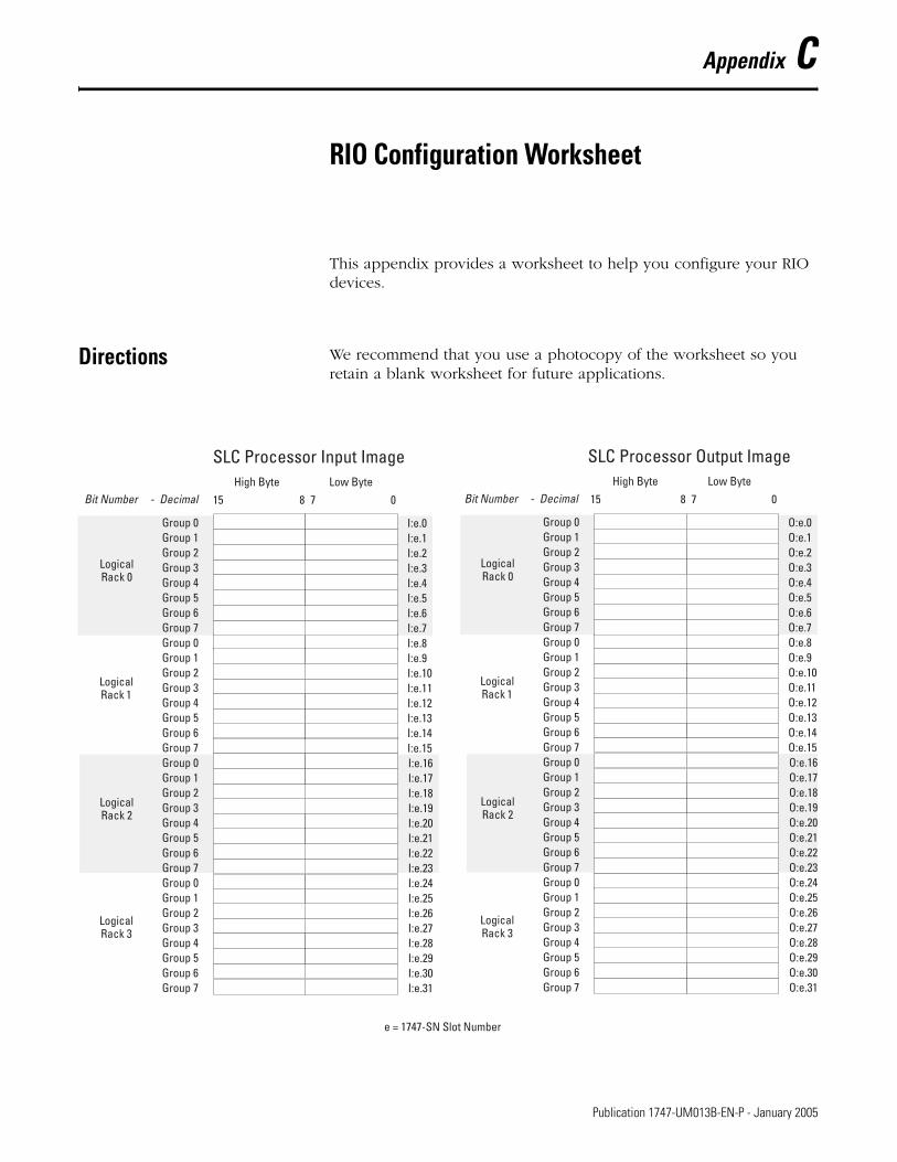
Appendix C
RIO Configuration Worksheet
This appendix provides a worksheet to help you configure your RIO devices.
Directions We recommend that you use a photocopy of the worksheet so you retain a blank worksheet for future applications.
Bit Number - Decimal
LogicalRack 1
07815
LogicalRack 0
LogicalRack 2
LogicalRack 3
SLC Processor Input Image
I:e.0I:e.1I:e.2I:e.3I:e.4I:e.5I:e.6I:e.7I:e.8I:e.9I:e.10I:e.11I:e.12I:e.13I:e.14I:e.15I:e.16I:e.17I:e.18I:e.19I:e.20I:e.21I:e.22I:e.23I:e.24I:e.25I:e.26I:e.27I:e.28I:e.29I:e.30I:e.31
Group 0Group 1Group 2Group 3Group 4Group 5Group 6Group 7Group 0Group 1Group 2Group 3Group 4Group 5Group 6Group 7Group 0Group 1Group 2Group 3Group 4Group 5Group 6Group 7Group 0Group 1Group 2Group 3Group 4Group 5Group 6Group 7
High Byte Low ByteBit Number - Decimal
LogicalRack 1
07815
LogicalRack 0
LogicalRack 2
LogicalRack 3
SLC Processor Output Image
O:e.0O:e.1O:e.2O:e.3O:e.4O:e.5O:e.6O:e.7O:e.8O:e.9O:e.10O:e.11O:e.12O:e.13O:e.14O:e.15O:e.16O:e.17O:e.18O:e.19O:e.20O:e.21O:e.22O:e.23O:e.24O:e.25O:e.26O:e.27O:e.28O:e.29O:e.30O:e.31
Group 0Group 1Group 2Group 3Group 4Group 5Group 6Group 7Group 0Group 1Group 2Group 3Group 4Group 5Group 6Group 7Group 0Group 1Group 2Group 3Group 4Group 5Group 6Group 7Group 0Group 1Group 2Group 3Group 4Group 5Group 6Group 7
High Byte Low Byte
e = 1747-SN Slot Number
1 Publication 1747-UM013B-EN-P - January 2005

C-2 RIO Configuration Worksheet
Bit Number - Decimal
LogicalRack 1
07815
LogicalRack 0
LogicalRack 2
LogicalRack 3
SLC Processor Input Image
I:e.0I:e.1I:e.2I:e.3I:e.4I:e.5I:e.6I:e.7I:e.8I:e.9I:e.10I:e.11I:e.12I:e.13I:e.14I:e.15I:e.16I:e.17I:e.18I:e.19I:e.20I:e.21I:e.22I:e.23I:e.24I:e.25I:e.26I:e.27I:e.28I:e.29I:e.30I:e.31
Group 0Group 1Group 2Group 3Group 4Group 5Group 6Group 7Group 0Group 1Group 2Group 3Group 4Group 5Group 6Group 7Group 0Group 1Group 2Group 3Group 4Group 5Group 6Group 7Group 0Group 1Group 2Group 3Group 4Group 5Group 6Group 7
High Byte Low ByteBit Number - Decimal
LogicalRack 1
07815
LogicalRack 0
LogicalRack 2
LogicalRack 3
SLC Processor Output Image
O:e.0O:e.1O:e.2O:e.3O:e.4O:e.5O:e.6O:e.7O:e.8O:e.9O:e.10O:e.11O:e.12O:e.13O:e.14O:e.15O:e.16O:e.17O:e.18O:e.19O:e.20O:e.21O:e.22O:e.23O:e.24O:e.25O:e.26O:e.27O:e.28O:e.29O:e.30O:e.31
Group 0Group 1Group 2Group 3Group 4Group 5Group 6Group 7Group 0Group 1Group 2Group 3Group 4Group 5Group 6Group 7Group 0Group 1Group 2Group 3Group 4Group 5Group 6Group 7Group 0Group 1Group 2Group 3Group 4Group 5Group 6Group 7
High Byte Low Byte
e = 1747-SN Slot Number
Publication 1747-UM013B-EN-P - January 2005
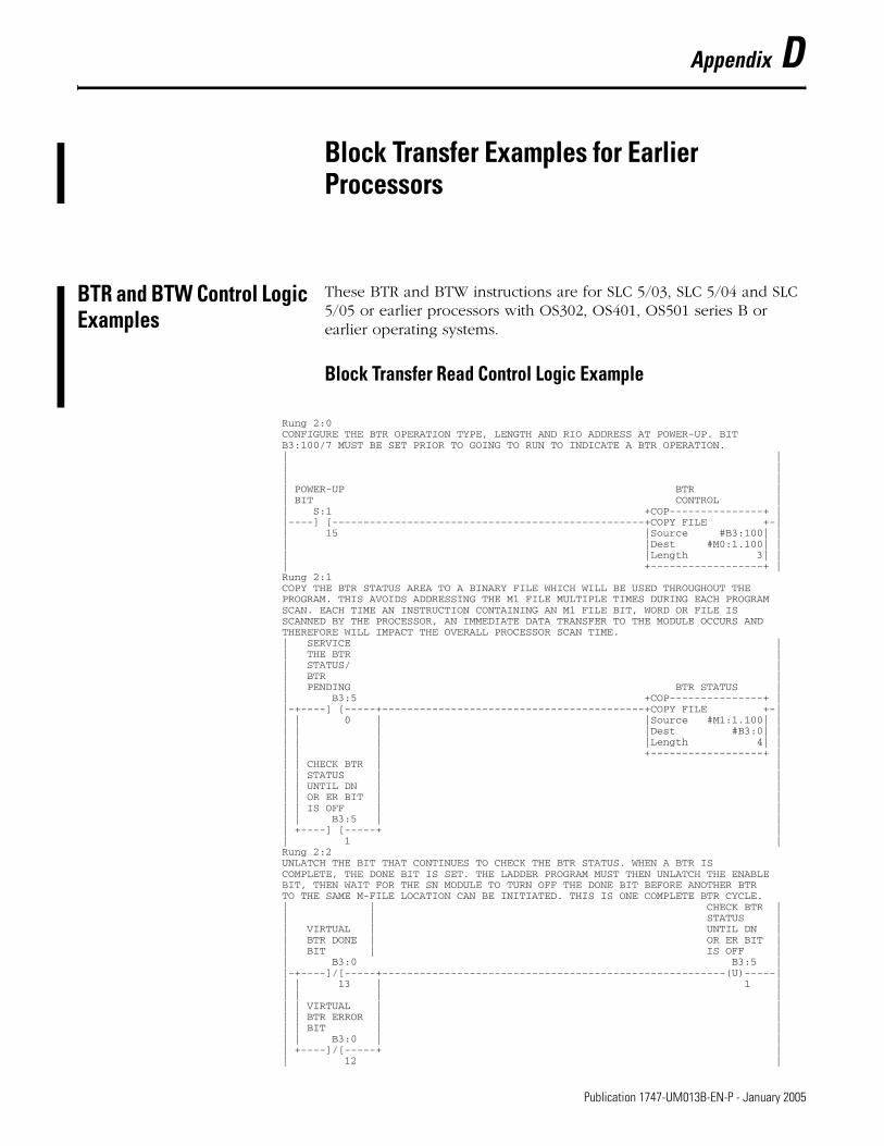
Appendix D
Block Transfer Examples for Earlier Processors
BTR and BTW Control Logic Examples
These BTR and BTW instructions are for SLC 5/03, SLC 5/04 and SLC 5/05 or earlier processors with OS302, OS401, OS501 series B or earlier operating systems.
Block Transfer Read Control Logic Example
Rung 2:0 CONFIGURE THE BTR OPERATION TYPE, LENGTH AND RIO ADDRESS AT POWER-UP. BIT B3:100/7 MUST BE SET PRIOR TO GOING TO RUN TO INDICATE A BTR OPERATION. | | | | | | | POWER-UP BTR | | BIT CONTROL | | S:1 +COP---------------+ | |----] [--------------------------------------------------+COPY FILE +-| | 15 |Source #B3:100| | | |Dest #M0:1.100| | | |Length 3| | | +------------------+ | Rung 2:1 COPY THE BTR STATUS AREA TO A BINARY FILE WHICH WILL BE USED THROUGHOUT THE PROGRAM. THIS AVOIDS ADDRESSING THE M1 FILE MULTIPLE TIMES DURING EACH PROGRAM SCAN. EACH TIME AN INSTRUCTION CONTAINING AN M1 FILE BIT, WORD OR FILE IS SCANNED BY THE PROCESSOR, AN IMMEDIATE DATA TRANSFER TO THE MODULE OCCURS AND THEREFORE WILL IMPACT THE OVERALL PROCESSOR SCAN TIME. | SERVICE | | THE BTR | | STATUS/ | | BTR | | PENDING BTR STATUS | | B3:5 +COP---------------+ | |-+----] [-----+------------------------------------------+COPY FILE +-| | | 0 | |Source #M1:1.100| | | | | |Dest #B3:0| | | | | |Length 4| | | | | +------------------+ | | | CHECK BTR | | | | STATUS | | | | UNTIL DN | | | | OR ER BIT | | | | IS OFF | | | | B3:5 | | | +----] [-----+ | | 1 | Rung 2:2 UNLATCH THE BIT THAT CONTINUES TO CHECK THE BTR STATUS. WHEN A BTR IS COMPLETE, THE DONE BIT IS SET. THE LADDER PROGRAM MUST THEN UNLATCH THE ENABLE BIT, THEN WAIT FOR THE SN MODULE TO TURN OFF THE DONE BIT BEFORE ANOTHER BTR TO THE SAME M-FILE LOCATION CAN BE INITIATED. THIS IS ONE COMPLETE BTR CYCLE. | | CHECK BTR | | | STATUS | | VIRTUAL | UNTIL DN | | BTR DONE | OR ER BIT | | BIT | IS OFF | | B3:0 B3:5 | |-+----]/[-----+-------------------------------------------------------(U)-----| | | 13 | 1 | | | | | | | VIRTUAL | | | | BTR ERROR | | | | BIT | | | | B3:0 | | | +----]/[-----+ | | 12 |
1 Publication 1747-UM013B-EN-P - January 2005
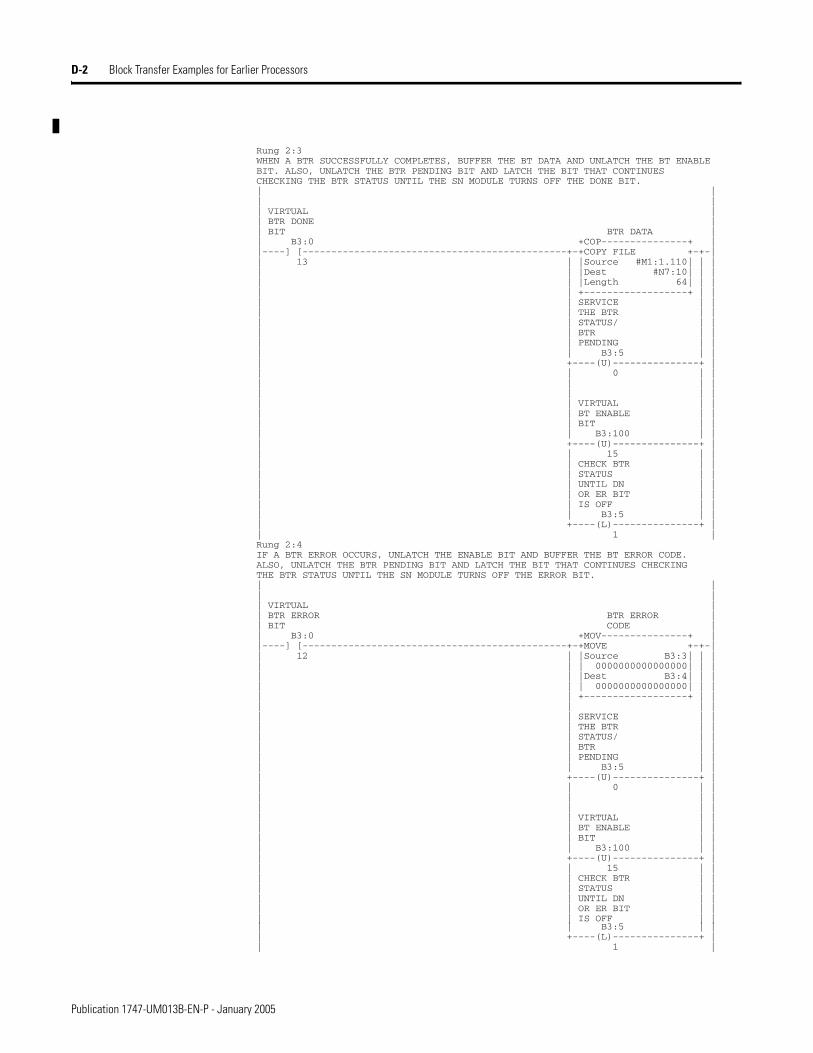
D-2 Block Transfer Examples for Earlier Processors
Rung 2:3 WHEN A BTR SUCCESSFULLY COMPLETES, BUFFER THE BT DATA AND UNLATCH THE BT ENABLE BIT. ALSO, UNLATCH THE BTR PENDING BIT AND LATCH THE BIT THAT CONTINUES CHECKING THE BTR STATUS UNTIL THE SN MODULE TURNS OFF THE DONE BIT. | | | | | VIRTUAL | | BTR DONE | | BIT BTR DATA | | B3:0 +COP---------------+ | |----] [----------------------------------------------+-+COPY FILE +-+-| | 13 | |Source #M1:1.110| | | | | |Dest #N7:10| | | | | |Length 64| | | | | +------------------+ | | | | SERVICE | | | | THE BTR | | | | STATUS/ | | | | BTR | | | | PENDING | | | | B3:5 | | | +----(U)---------------+ | | | 0 | | | | | | | | | | | | VIRTUAL | | | | BT ENABLE | | | | BIT | | | | B3:100 | | | +----(U)---------------+ | | | 15 | | | | CHECK BTR | | | | STATUS | | | | UNTIL DN | | | | OR ER BIT | | | | IS OFF | | | | B3:5 | | | +----(L)---------------+ | | 1 | Rung 2:4 IF A BTR ERROR OCCURS, UNLATCH THE ENABLE BIT AND BUFFER THE BT ERROR CODE. ALSO, UNLATCH THE BTR PENDING BIT AND LATCH THE BIT THAT CONTINUES CHECKING THE BTR STATUS UNTIL THE SN MODULE TURNS OFF THE ERROR BIT. | | | | | VIRTUAL | | BTR ERROR BTR ERROR | | BIT CODE | | B3:0 +MOV---------------+ | |----] [----------------------------------------------+-+MOVE +-+-| | 12 | |Source B3:3| | | | | | 0000000000000000| | | | | |Dest B3:4| | | | | | 0000000000000000| | | | | +------------------+ | | | | | | | | SERVICE | | | | THE BTR | | | | STATUS/ | | | | BTR | | | | PENDING | | | | B3:5 | | | +----(U)---------------+ | | | 0 | | | | | | | | | | | | VIRTUAL | | | | BT ENABLE | | | | BIT | | | | B3:100 | | | +----(U)---------------+ | | | 15 | | | | CHECK BTR | | | | STATUS | | | | UNTIL DN | | | | OR ER BIT | | | | IS OFF | | | | B3:5 | | | +----(L)---------------+ | | 1 |
Publication 1747-UM013B-EN-P - January 2005
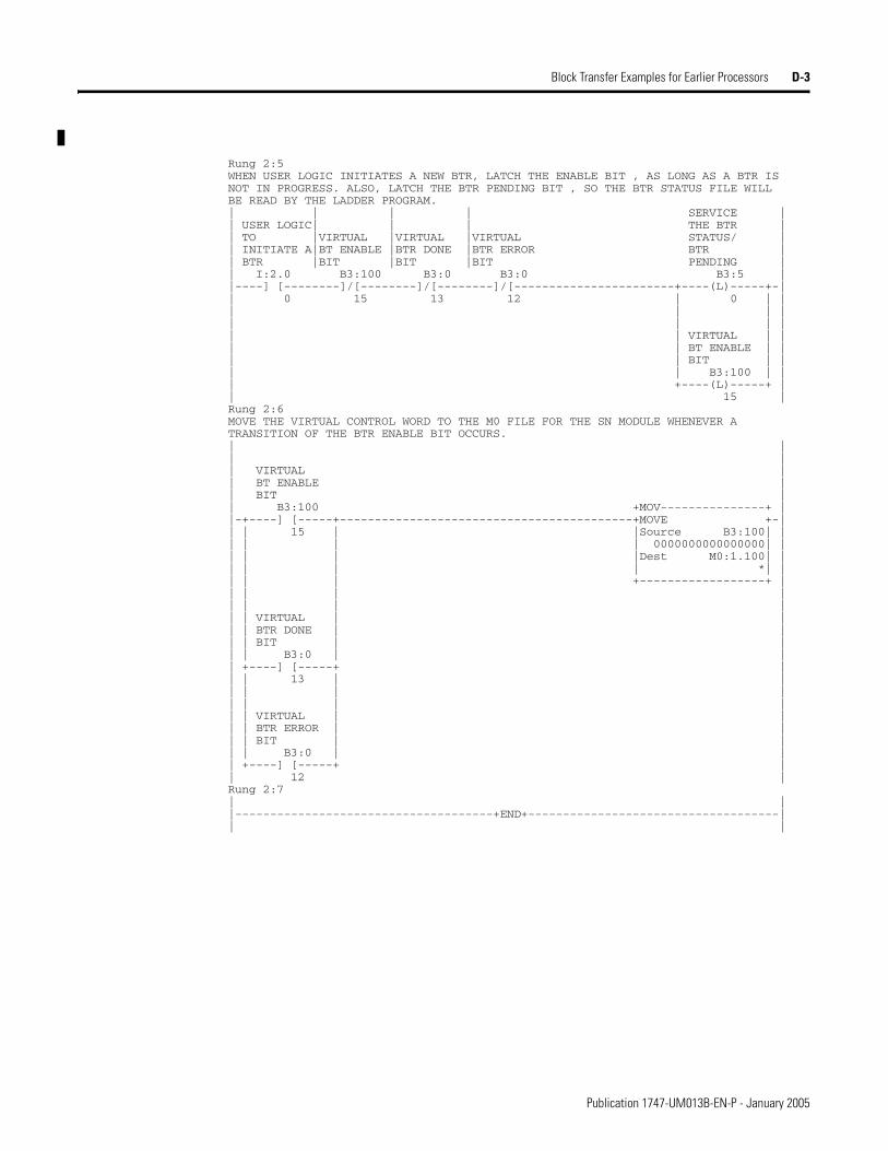
Block Transfer Examples for Earlier Processors D-3
Rung 2:5 WHEN USER LOGIC INITIATES A NEW BTR, LATCH THE ENABLE BIT , AS LONG AS A BTR IS NOT IN PROGRESS. ALSO, LATCH THE BTR PENDING BIT , SO THE BTR STATUS FILE WILL BE READ BY THE LADDER PROGRAM. | | | | SERVICE | | USER LOGIC| | | THE BTR | | TO |VIRTUAL |VIRTUAL |VIRTUAL STATUS/ | | INITIATE A|BT ENABLE |BTR DONE |BTR ERROR BTR | | BTR |BIT |BIT |BIT PENDING | | I:2.0 B3:100 B3:0 B3:0 B3:5 | |----] [--------]/[--------]/[--------]/[-----------------------+----(L)-----+-| | 0 15 13 12 | 0 | | | | | | | | | | | | VIRTUAL | | | | BT ENABLE | | | | BIT | | | | B3:100 | | | +----(L)-----+ | | 15 | Rung 2:6 MOVE THE VIRTUAL CONTROL WORD TO THE M0 FILE FOR THE SN MODULE WHENEVER A TRANSITION OF THE BTR ENABLE BIT OCCURS. | | | | | VIRTUAL | | BT ENABLE | | BIT | | B3:100 +MOV---------------+ | |-+----] [-----+------------------------------------------+MOVE +-| | | 15 | |Source B3:100| | | | | | 0000000000000000| | | | | |Dest M0:1.100| | | | | | *| | | | | +------------------+ | | | | | | | | | | | VIRTUAL | | | | BTR DONE | | | | BIT | | | | B3:0 | | | +----] [-----+ | | | 13 | | | | | | | | | | | | VIRTUAL | | | | BTR ERROR | | | | BIT | | | | B3:0 | | | +----] [-----+ | | 12 | Rung 2:7 | | |-------------------------------------+END+------------------------------------| | |
Publication 1747-UM013B-EN-P - January 2005

D-4 Block Transfer Examples for Earlier Processors
Block Transfer Write Control Logic Example
Rung 2:0 CONFIGURE THE BTW LENGTH AND RIO ADDRESS AT POWER-UP. ALSO, BE SURE THE BLOCK TRANSFER OPERATION BIT IS A ”0” INDICATING A BTW. ALL THESE PARAMETERS MUST BE ENTERED PRIOR TO PLACING THE PROCESSOR IN THE RUN MODE. | | | | | | | POWER-UP | | BIT | | S:1 +COP---------------+ | |----] [--------------------------------------------------+COPY FILE +-| | 15 |Source #B3:100| | | |Dest #M0:1.100| | | |Length 3| | | +------------------+ | Rung 2:1 COPY THE BTW STATUS AREA TO A BINARY FILE WHICH WILL BE USED THROUGHOUT THE PROGRAM, ONLY WHEN A BTW IS PENDING. THIS AVOIDS ACCESSING THE M1 FILE MULTIPLE TIMES DURING EACH PROGRAM SCAN. EACH TIME AN INSTRUCTION CONTAINING AN M1 FILE BIT, WORD OR FILE IS SCANNED BY THE PROCESSOR,AN IMMEDIATE DATA TRANSFER TO THE MODULE OCCURS AND THEREFORE WILL IMPACT THE PROCESSOR SCAN TIME. | SERVICE | | THE BTW | | STATUS/ | | BTW | | PENDING BTW STATUS | | B3:5 +COP---------------+ | |-+----] [-----+------------------------------------------+COPY FILE +-| | | 0 | |Source #M1:1.100| | | | | |Dest #B3:0| | | | | |Length 4| | | | | +------------------+ | | | | | | | CHECK BTW | | | | STATUS | | | | UNTIL DONE | | | | BIT IS OFF | | | | B3:5 | | | +----] [-----+ | | 1 | Rung 2:2 UNLATCH THE BIT THAT CONTINUES TO CHECK THE BTW STATUS. WHEN A BTW IS COMPLETE, THE DONE BIT IS SET. THE LADDER PROGRAM MUST THEN UNLATCH THE ENABLE BIT, THEN WAIT FOR THE SN MODULE TO TURN OFF THE DONE BIT BEFORE ANOTHER BTW TO THE SAME M-FILE LOCATION CAN BE INITIALIZED. THIS IS ONE COMPLETE BTW CYCLE. | | | | | CHECK BTW | | VIRTUAL | STATUS | | BTW DONE | UNTIL DONE | | BIT | BIT IS OFF | | B3:0 B3:5 | |-+----]/[-----+-------------------------------------------------------(U)-----| | | 13 | 1 | | | | | | | VIRTUAL | | | | BTW ERROR | | | | BIT | | | | B3:0 | | | +----]/[-----+ | | 12 | Rung 2:3 WHEN A BTW SUCCESSFULLY COMPLETES, UNLATCH THE BTW ENABLE BIT. ALSO, UNLATCH THE BTW PENDING BIT AND LATCH THE BIT THAT CONTINUES CHECKING THE BTW STATUS UNTIL THE SN MODULE TURNS OFF THE DONE BIT. | SERVICE | | THE BTW | | VIRTUAL STATUS/ | | BTW DONE BTW | | BIT PENDING | | B3:0 B3:5 | |----] [--------------------------------------------------------+----(U)-----+-| | 13 | 0 | | | | | | | | | | | | VIRTUAL | | | | BTW ENABLE | | | | BIT | | | | B3:100 | | | +----(U)-----+ | | | 15 | | | | | | | | CHECK BTW | | | | STATUS | | | | UNTIL DONE | | | | BIT IS OFF | | | | B3:5 | | | +----(L)-----+ | | 1 |
Publication 1747-UM013B-EN-P - January 2005
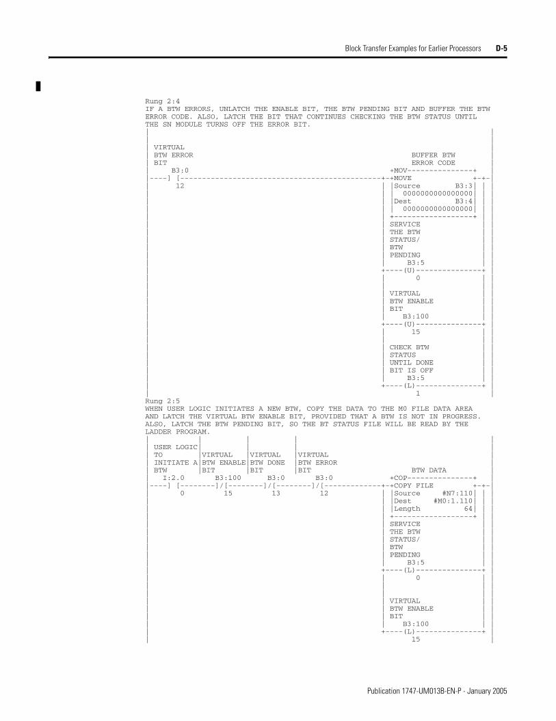
Block Transfer Examples for Earlier Processors D-5
Rung 2:4 IF A BTW ERRORS, UNLATCH THE ENABLE BIT, THE BTW PENDING BIT AND BUFFER THE BTW ERROR CODE. ALSO, LATCH THE BIT THAT CONTINUES CHECKING THE BTW STATUS UNTIL THE SN MODULE TURNS OFF THE ERROR BIT. | | | | | VIRTUAL | | BTW ERROR BUFFER BTW | | BIT ERROR CODE | | B3:0 +MOV---------------+ | |----] [----------------------------------------------+-+MOVE +-+-| | 12 | |Source B3:3| | | | | | 0000000000000000| | | | | |Dest B3:4| | | | | | 0000000000000000| | | | | +------------------+ | | | | SERVICE | | | | THE BTW | | | | STATUS/ | | | | BTW | | | | PENDING | | | | B3:5 | | | +----(U)---------------+ | | | 0 | | | | | | | | VIRTUAL | | | | BTW ENABLE | | | | BIT | | | | B3:100 | | | +----(U)---------------+ | | | 15 | | | | | | | | CHECK BTW | | | | STATUS | | | | UNTIL DONE | | | | BIT IS OFF | | | | B3:5 | | | +----(L)---------------+ | | 1 | Rung 2:5 WHEN USER LOGIC INITIATES A NEW BTW, COPY THE DATA TO THE M0 FILE DATA AREA AND LATCH THE VIRTUAL BTW ENABLE BIT, PROVIDED THAT A BTW IS NOT IN PROGRESS. ALSO, LATCH THE BTW PENDING BIT, SO THE BT STATUS FILE WILL BE READ BY THE LADDER PROGRAM. | | | | | | USER LOGIC| | | | | TO |VIRTUAL |VIRTUAL |VIRTUAL | | INITIATE A|BTW ENABLE|BTW DONE |BTW ERROR | | BTW |BIT |BIT |BIT BTW DATA | | I:2.0 B3:100 B3:0 B3:0 +COP---------------+ | |----] [--------]/[--------]/[--------]/[-------------+-+COPY FILE +-+-| | 0 15 13 12 | |Source #N7:110| | | | | |Dest #M0:1.110| | | | | |Length 64| | | | | +------------------+ | | | | SERVICE | | | | THE BTW | | | | STATUS/ | | | | BTW | | | | PENDING | | | | B3:5 | | | +----(L)---------------+ | | | 0 | | | | | | | | | | | | VIRTUAL | | | | BTW ENABLE | | | | BIT | | | | B3:100 | | | +----(L)---------------+ | | 15 |
Publication 1747-UM013B-EN-P - January 2005

D-6 Block Transfer Examples for Earlier Processors
Directional Continuous Block Transfer Example
The following rungs demonstrate a directional continuous block transfer. As long as the BTR precondition bit is true, block transfer reads execute continuously. Use the same method for a BTW.
Rung 2:6 MOVE THE VIRTUAL CONTROL WORD TO THE M0 FILE FOR THE SN MODULE WHENEVER A TRANSITION OF THE BTW ENABLE BIT OCCURS. | | | | | VIRTUAL | | BTW ENABLE | | BIT | | B3:100 +MOV---------------+ | |-+----] [-----+------------------------------------------+MOVE +-| | | 15 | |Source B3:100| | | | | | 0000000000000000| | | | | |Dest M0:1.100| | | | | | *| | | | | +------------------+ | | | | | | | | | | | VIRTUAL | | | | BTW DONE | | | | BIT | | | | B3:0 | | | +----] [-----+ | | | 13 | | | | | | | | | | | | VIRTUAL | | | | BTW ERROR | | | | BIT | | | | B3:0 | | | +----] [-----+ | | 12 | Rung 2:7 | | |-------------------------------------+END+------------------------------------| | |
Publication 1747-UM013B-EN-P - January 2005

Block Transfer Examples for Earlier Processors D-7
Rung 2:0 CONFIGURE THE BTR OPERATION TYPE, LENGTH AND RIO ADDRESS AT POWER-UP. BIT B3:100/7 MUST BE SET PRIOR TO GOING TO RUN TO INDICATE A BTR OPERATION. | | | | | | | POWER-UP BTR | | BIT CONTROL | | S:1 +COP---------------+ | |----] [--------------------------------------------------+COPY FILE +-| | 15 |Source #B3:100| | | |Dest #M0:1.100| | | |Length 3| | | +------------------+ |
Rung 2:1 COPY THE BTR STATUS AREA TO A BINARY FILE WHICH WILL BE USED THROUGHOUT THE PROGRAM. THIS AVOIDS ADDRESSING THE M1 FILE MULTIPLE TIMES DURING EACH PROGRAM SCAN. EACH TIME AN INSTRUCTION CONTAINING AN M1 FILE BIT, WORD OR FILE IS SCANNED BY THE PROCESSOR, AN IMMEDIATE DATA TRANSFER TO THE MODULE OCCURS AND THEREFORE WILL IMPACT THE OVERALL PROCESSOR SCAN TIME. | | | | | | | BTR | | PENDING BTR STATUS | | B3 +COP---------------+ | |-+----] [-----+------------------------------------------+COPY FILE +-| | | 80 | |Source #M1:1.100| | | | | |Dest #B3:0| | | | | |Length 4| | | | | +------------------+ | | | | | | | | | | | | | | | CHECK BTR | | | | STATUS | | | | B3 | | | +----] [-----+ | | 81 | Rung 2:2 WHEN THE ERROR OR DONE BIT IS SET INDICATING THAT THE BTR COMPLETED EITHER UNSUCCESSFULLY OR SUCCESSFULLY, THE ENABLE BIT MUST BE UNLATCHED BY THE LADDER PROGRAM. THE 1747-SN SCANNER THEN UNLATCHES THE ERROR/DONE BIT TO COMPLETE THE BLOCK TRANSFER HAND-SHAKE PROCESS. AT THIS TIME THE ”CHECK BTR STATUS” BIT MUST BE UNLATCHED TO AVOID UNNECESSARY M-FILE ACCESSES. | | | | | VIRTUAL | | BTR DONE CHECK BTR | | BIT STATUS | | B3 B3 | |-+----]/[-----+-------------------------------------------------------(U)-----| | | 13 | 81 | | | | | | | | | | | | | | | | | | | VIRTUAL | | | | BT ERROR | | | | BIT | | | | B3 | | | +----]/[-----+ | | 12 |
Publication 1747-UM013B-EN-P - January 2005
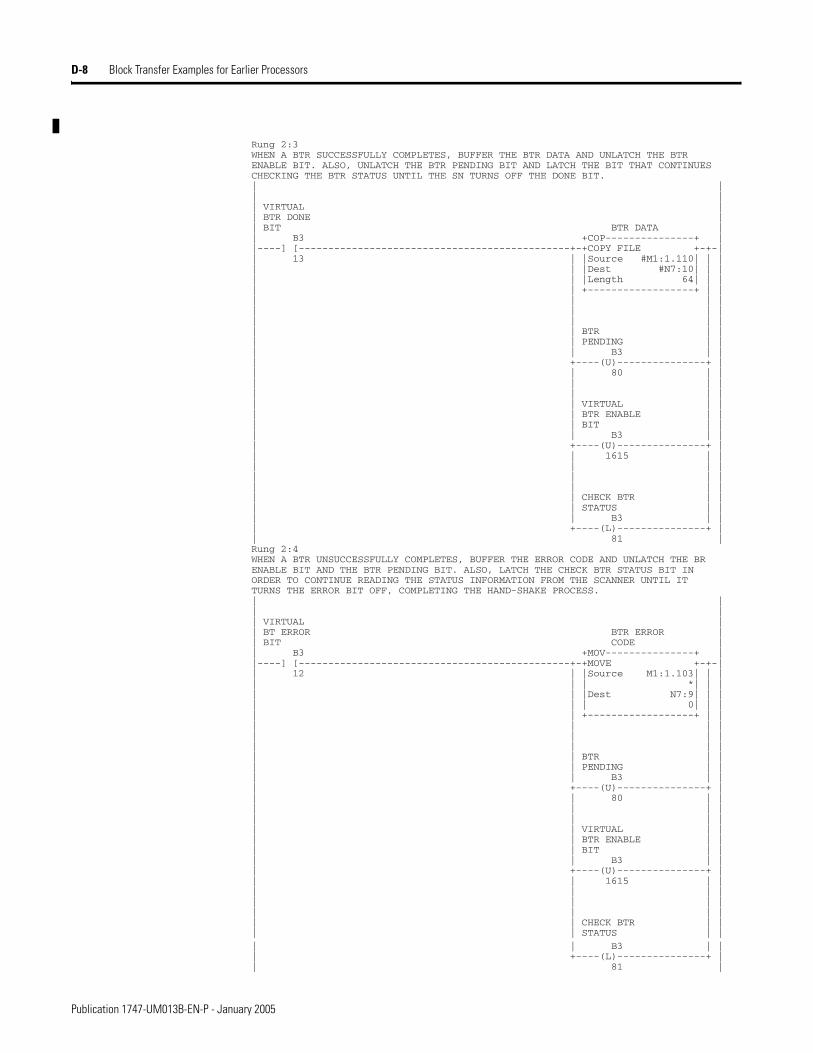
D-8 Block Transfer Examples for Earlier Processors
Rung 2:3 WHEN A BTR SUCCESSFULLY COMPLETES, BUFFER THE BTR DATA AND UNLATCH THE BTR ENABLE BIT. ALSO, UNLATCH THE BTR PENDING BIT AND LATCH THE BIT THAT CONTINUES CHECKING THE BTR STATUS UNTIL THE SN TURNS OFF THE DONE BIT. | | | | | VIRTUAL | | BTR DONE | | BIT BTR DATA | | B3 +COP---------------+ | |----] [----------------------------------------------+-+COPY FILE +-+-| | 13 | |Source #M1:1.110| | | | | |Dest #N7:10| | | | | |Length 64| | | | | +------------------+ | | | | | | | | | | | | | | | | BTR | | | | PENDING | | | | B3 | | | +----(U)---------------+ | | | 80 | | | | | | | | | | | | VIRTUAL | | | | BTR ENABLE | | | | BIT | | | | B3 | | | +----(U)---------------+ | | | 1615 | | | | | | | | | | | | | | | | CHECK BTR | | | | STATUS | | | | B3 | | | +----(L)---------------+ | | 81 | Rung 2:4 WHEN A BTR UNSUCCESSFULLY COMPLETES, BUFFER THE ERROR CODE AND UNLATCH THE BR ENABLE BIT AND THE BTR PENDING BIT. ALSO, LATCH THE CHECK BTR STATUS BIT IN ORDER TO CONTINUE READING THE STATUS INFORMATION FROM THE SCANNER UNTIL IT TURNS THE ERROR BIT OFF, COMPLETING THE HAND-SHAKE PROCESS. | | | | | VIRTUAL | | BT ERROR BTR ERROR | | BIT CODE | | B3 +MOV---------------+ | |----] [----------------------------------------------+-+MOVE +-+-| | 12 | |Source M1:1.103| | | | | | *| | | | | |Dest N7:9| | | | | | 0| | | | | +------------------+ | | | | | | | | | | | | | | | | BTR | | | | PENDING | | | | B3 | | | +----(U)---------------+ | | | 80 | | | | | | | | | | | | VIRTUAL | | | | BTR ENABLE | | | | BIT | | | | B3 | | | +----(U)---------------+ | | | 1615 | | | | | | | | | | | | | | | | CHECK BTR | | | | STATUS | |
| | B3 | | | +----(L)---------------+ | | 81 |
Publication 1747-UM013B-EN-P - January 2005

Block Transfer Examples for Earlier Processors D-9
Directional Repeating Block Transfer Example
The following example shows a directional repeating block transfer. This means that block transfer reads will be sent repeatedly, as fast as possible. Use the same method for a BTW.
Rung 2:5 BLOCK TRANSFER READS WILL EXECUTE CONTINUOUSLY AS LONG AS THE BTR PRECONDITION BIT IS TRUE. | | | | | | | | | | | BTR PRE- |VIRTUAL |VIRTUAL |VIRTUAL | | CONDITION |BTR ENABLE|BTR DONE |BT ERROR BTR | | BIT |BIT |BIT |BIT PENDING | | B3 B3 B3 B3 B3 | |----] [--------]/[--------]/[--------]/[-----------------------+----(L)-----+-| | 83 1615 13 12 | 80 | | | | | | | | | | | | | | | | | | | | VIRTUAL | | | | BTR ENABLE | | | | BIT | | | | B3 | | | +----(L)-----+ | | 1615 | Rung 2:6 MOVE THE VIRTUAL CONTROL WORD TO THE M0 FILE FOR THE SN MODULE WHILE A BTR IS IN PROGRESS, AND CONTINUE DOING SO UNTIL THE ENABLE, DONE AND ERROR BITS ARE ALL TURNED OFF, COMPLETING THE HAND-SHAKE PROCESS. | | | | | VIRTUAL BTR | | BTR ENABLE CONTROL | | BIT WORD | | B3 +MOV---------------+ | |-+----] [-----+------------------------------------------+MOVE +-| | | 1615 | |Source B3:100| | | | | | 0000000000000000| | | | | |Dest M0:1.100| | | | | | *| | | | | +------------------+ | | | | | | | | | | | VIRTUAL | | | | BTR DONE | | | | BIT | | | | B3 | | | +----] [-----+ | | | 13 | | | | | | | | | | | | VIRTUAL | | | | BT ERROR | | | | BIT | | | | B3 | | | +----] [-----+ | | 12 | Rung 2:7 | | |-------------------------------------+END+------------------------------------| | |
Publication 1747-UM013B-EN-P - January 2005

D-10 Block Transfer Examples for Earlier Processors
Rung 2:0 CONFIGURE THE BTR OPERATION TYPE, LENGTH AND RIO ADDRESS AT POWER-UP. BIT B3:100/7 MUST BE SET PRIOR TO GOING TO RUN TO INDICATE A BTR OPERATION. | | | | | | | POWER-UP BTR | | BIT CONTROL | | S:1 +COP---------------+ | |----] [--------------------------------------------------+COPY FILE +-| | 15 |Source #B3:100| | | |Dest #M0:1.100| | | |Length 3| | | +------------------+ | Rung 2:1 COPY THE BTR STATUS AREA TO A BINARY FILE WHICH WILL BE USED THROUGHOUT THE PROGRAM. THIS AVOIDS ADDRESSING THE M1 FILE MULTIPLE TIMES DURING EACH PROGRAM SCAN. EACH TIME AN INSTRUCTION CONTAINING AN M-FILE BIT, WORD OR FILE IS SCANNED BY THE PROCESSOR, AN IMMEDIATE DATA TRANSFER TO THE MODULE OCCURS AND THEREFORE WILL IMPACT THE OVERALL PROCESSOR SCAN TIME. | | | | | | | BTR | | PENDING BTR STATUS | | B3 +COP---------------+ | |-+----] [-----+------------------------------------------+COPY FILE +-| | | 80 | |Source #M1:1.100| | | | | |Dest #B3:0| | | | | |Length 4| | | | | +------------------+ | | | | | | | | | | | | | | | CHECK BTR | | | | STATUS | | | | B3 | | | +----] [-----+ | | 81 | Rung 2:2 UNLATCH THE BIT THAT CONTINUES TO CHECK THE BTR STATUS. WHEN A BTR IS COMPLETE, THE DONE OR ERROR BIT IS SET. THE LADDER PROGRAM MUST THEN UNLATCH THE ENABLE BIT, THEN WAIT FOR THE SN MODULE TO TURN OFF THE DONE/ERROR BIT BEFORE ANOTHER BTR TO THE SAME M-FILE LOCATION CAN BE INITIATED. THIS IS ONE COMPLETE BTR CYCLE. | | | | | VIRTUAL | | BTR DONE CHECK BTR | | BIT STATUS | | B3 B3 | |-+----]/[-----+-------------------------------------------------------(U)-----| | | 13 | 81 | | | | | | | | | | | | | | | | | | | VIRTUAL | | | | BT ERROR | | | | BIT | | | | B3 | | | +----]/[-----+ | | 12 |
Publication 1747-UM013B-EN-P - January 2005
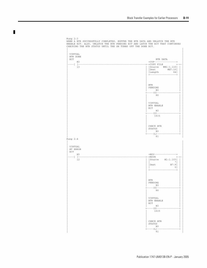
Block Transfer Examples for Earlier Processors D-11
Rung 2:3 WHEN A BTR SUCCESSFULLY COMPLETES, BUFFER THE BTR DATA AND UNLATCH THE BTR ENABLE BIT. ALSO, UNLATCH THE BTR PENDING BIT AND LATCH THE BIT THAT CONTINUES CHECKING THE BTR STATUS UNTIL THE SN TURNS OFF THE DONE BIT. | | | | | VIRTUAL | | BTR DONE | | BIT BTR DATA | | B3 +COP---------------+ | |----] [----------------------------------------------+-+COPY FILE +-+-| | 13 | |Source #M1:1.110| | | | | |Dest #N7:10| | | | | |Length 64| | | | | +------------------+ | | | | | | | | | | | | | | | | BTR | | | | PENDING | | | | B3 | | | +----(U)---------------+ | | | 80 | | | | | | | | | | | | VIRTUAL | | | | BTR ENABLE | | | | BIT | | | | B3 | | | +----(U)---------------+ | | | 1615 | | | | | | | | | | | | | | | | CHECK BTR | | | | STATUS | | | | B3 | | | +----(L)---------------+ | | 81 | Rung 2:4 | | | | | VIRTUAL | | BT ERROR | | BIT | | B3 +MOV---------------+ | |----] [----------------------------------------------+-+MOVE +-+-| | 12 | |Source M1:1.103| | | | | | *| | | | | |Dest N7:9| | | | | | 0| | | | | +------------------+ | | | | | | | | | | | | | | | | BTR | | | | PENDING | | | | B3 | | | +----(U)---------------+ | | | 80 | | | | | | | | | | | | VIRTUAL | | | | BTR ENABLE | | | | BIT | | | | B3 | | | +----(U)---------------+ | | | 1615 | | | | | | | | | | | | | | | | CHECK BTR | | | | STATUS | | | | B3 | | | +----(L)---------------+ | | 81 |
Publication 1747-UM013B-EN-P - January 2005
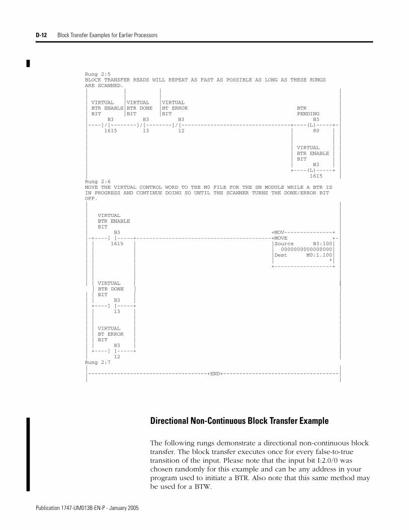
D-12 Block Transfer Examples for Earlier Processors
Directional Non-Continuous Block Transfer Example
The following rungs demonstrate a directional non-continuous block transfer. The block transfer executes once for every false-to-true transition of the input. Please note that the input bit I:2.0/0 was chosen randomly for this example and can be any address in your program used to initiate a BTR. Also note that this same method may be used for a BTW.
Rung 2:5 BLOCK TRANSFER READS WILL REPEAT AS FAST AS POSSIBLE AS LONG AS THESE RUNGS ARE SCANNED. | | | | | | | | | VIRTUAL |VIRTUAL |VIRTUAL | | BTR ENABLE|BTR DONE |BT ERROR BTR | | BIT |BIT |BIT PENDING | | B3 B3 B3 B3 | |----]/[--------]/[--------]/[----------------------------------+----(L)-----+-| | 1615 13 12 | 80 | | | | | | | | | | | | VIRTUAL | | | | BTR ENABLE | | | | BIT | | | | B3 | | | +----(L)-----+ | | 1615 | Rung 2:6 MOVE THE VIRTUAL CONTROL WORD TO THE M0 FILE FOR THE SN MODULE WHILE A BTR IS IN PROGRESS AND CONTINUE DOING SO UNTIL THE SCANNER TURNS THE DONE/ERROR BIT OFF. | | | | | VIRTUAL | | BTR ENABLE | | BIT | | B3 +MOV---------------+ | |-+----] [-----+------------------------------------------+MOVE +-| | | 1615 | |Source B3:100| | | | | | 0000000000000000| | | | | |Dest M0:1.100| | | | | | *| | | | | +------------------+ | | | | | | | | | | | VIRTUAL | | |
| BTR DONE | | | | BIT | | | | B3 | | | +----] [-----+ | | | 13 | | | | | | | | | | | | VIRTUAL | | | | BT ERROR | | | | BIT | | | | B3 | | | +----] [-----+ | | 12 | Rung 2:7 | | |-------------------------------------+END+------------------------------------| | |
Publication 1747-UM013B-EN-P - January 2005

Block Transfer Examples for Earlier Processors D-13
Rung 2:0 CONFIGURE THE BTR OPERATION TYPE, LENGTH AND RIO ADDRESS AT POWER-UP. BIT B3:100/7 MUST BE SET PRIOR TO GOING TO RUN TO INDICATE A BTR OPERATION. | | | | | | | POWER-UP BTR | | BIT CONTROL | | S:1 +COP---------------+ | |----] [--------------------------------------------------+COPY FILE +-| | 15 |Source #B3:100| | | |Dest #M0:1.100| | | |Length 3| | | +------------------+ | Rung 2:1 COPY THE BTR STATUS AREA TO A BINARY FILE WHICH WILL BE USED THROUGHOUT THE PROGRAM. THIS AVOIDS ADDRESSING THE M1 FILE MULTIPLE TIMES DURING EACH PROGRAM SCAN. EACH TIME AN INSTRUCTION CONTAINING AN M1 FILE BIT, WORD OR FILE IS SCANNED BY THE PROCESSOR, AN IMMEDIATE DATA TRANSFER TO THE MODULE OCCURS AND THEREFORE WILL IMPACT THE OVERALL PROCESSOR SCAN TIME. | | | | | | | BTR | | PENDING BTR STATUS | | B3 +COP---------------+ | |-+----] [-----+------------------------------------------+COPY FILE +-| | | 80 | |Source #M1:1.100| | | | | |Dest #B3:0| | | | | |Length 4| | | | | +------------------+ | | | | | | | | | | | | | | | CHECK BTR | | | | STATUS | | | | B3 | | | +----] [-----+ | | 81 | Rung 2:2 UNLATCH THE BIT THAT CONTINUES TO CHECK THE BTR STATUS. WHEN A BTR IS COMPLETE, THE DONE OR ERROR BIT IS SET. THE LADDER PROGRAM MUST THEN UNLATCH THE ENABLE BIT, THEN WAIT FOR THE SN MODULE TO TURN OFF THE DONE/ERROR BIT BEFORE ANOTHER BTR TO THE SAME M-FILE LOCATION CAN BE INITIATED. THIS IS ONE COMPLETE BTR CYCLE. | | | | | VIRTUAL | | BTR DONE CHECK BTR | | BIT STATUS | | B3 B3 | |-+----]/[-----+-------------------------------------------------------(U)-----| | | 13 | 81 | | | | | | | | | | | | | | | | | | | VIRTUAL | | | | BTR ERROR | | | | BIT | | | | B3 | | | +----]/[-----+ | | 12 |
Publication 1747-UM013B-EN-P - January 2005

D-14 Block Transfer Examples for Earlier Processors
Rung 2:3 WHEN A BTR SUCCESSFULLY COMPLETES, BUFFER THE BTR DATA AND UNLATCH THE BTR ENABLE BIT. ALSO, UNLATCH THE BTR PENDING BIT AND LATCH THE BIT THAT CONTINUES CHECKING THE BTR STATUS UNTIL THE SN TURNS OFF THE DONE BIT. | | | | | VIRTUAL | | BTR DONE | | BIT BTR DATA | | B3 +COP---------------+ | |----] [----------------------------------------------+-+COPY FILE +-+-| | 13 | |Source #M1:1.110| | | | | |Dest #N7:10| | | | | |Length 64| | | | | +------------------+ | | | | | | | | | | | | | | | | BTR | | | | PENDING | | | | B3 | | | +----(U)---------------+ | | | 80 | | | | | | | | | | | | VIRTUAL | | | | BTR ENABLE | | | | BIT | | | | B3 | | | +----(U)---------------+ | | | 1615 | | | | | | | | | | | | | | | | CHECK BTR | | | | STATUS | | | | B3 | | | +----(L)---------------+ | | 81 | Rung 2:4 | | | | | VIRTUAL | | BTR ERROR | | BIT | | B3 +MOV---------------+ | |----] [----------------------------------------------+-+MOVE +-+-| | 12 | |Source M1:1.103| | | | | | *| | | | | |Dest N7:9| | | | | | 0| | | | | +------------------+ | | | | | | | | | | | | | | | | BTR | | | | PENDING | | | | B3 | | | +----(U)---------------+ | | | 80 | | | | | | | | | | | | VIRTUAL | | | | BTR ENABLE | | | | BIT | | | | B3 | | | +----(U)---------------+ | | | 1615 | | | | | | | | | | | | | | | | CHECK BTR | | | | STATUS | | | | B3 | | | +----(L)---------------+ | | 81 |
Publication 1747-UM013B-EN-P - January 2005
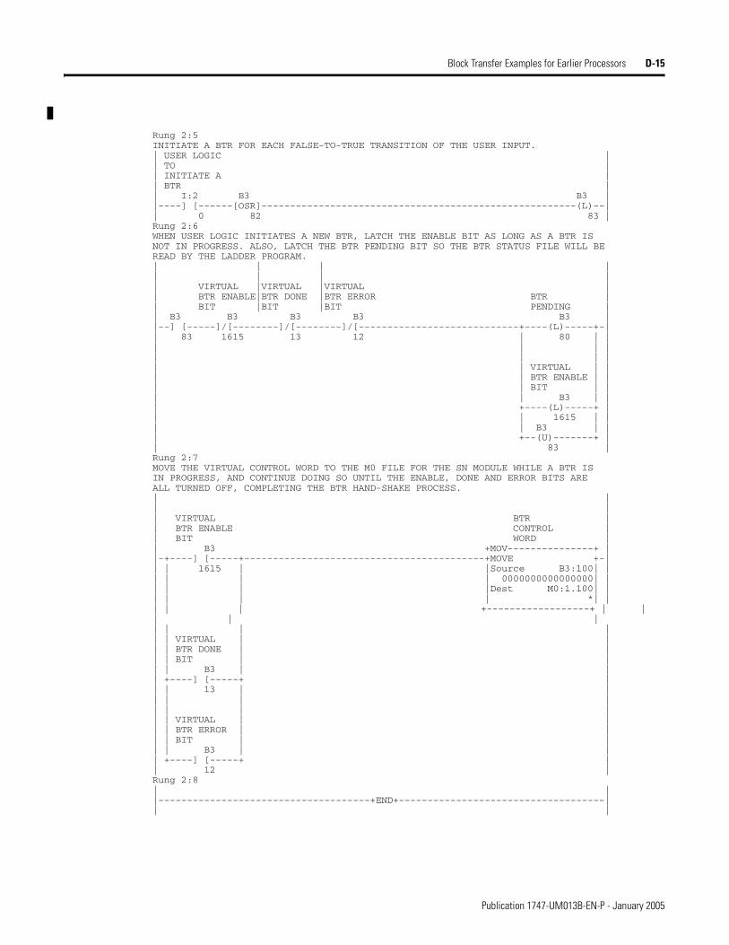
Block Transfer Examples for Earlier Processors D-15
Rung 2:5 INITIATE A BTR FOR EACH FALSE-TO-TRUE TRANSITION OF THE USER INPUT. | USER LOGIC | | TO | | INITIATE A | | BTR | | I:2 B3 B3 | |----] [------[OSR]-------------------------------------------------------(L)--| | 0 82 83 | Rung 2:6 WHEN USER LOGIC INITIATES A NEW BTR, LATCH THE ENABLE BIT AS LONG AS A BTR IS NOT IN PROGRESS. ALSO, LATCH THE BTR PENDING BIT SO THE BTR STATUS FILE WILL BE READ BY THE LADDER PROGRAM. | | | | | | | | | VIRTUAL |VIRTUAL |VIRTUAL | | BTR ENABLE|BTR DONE |BTR ERROR BTR | | BIT |BIT |BIT PENDING | | B3 B3 B3 B3 B3 | |--] [-----]/[--------]/[--------]/[----------------------------+----(L)-----+-| | 83 1615 13 12 | 80 | | | | | | | | | | | | VIRTUAL | | | | BTR ENABLE | | | | BIT | | | | B3 | | | +----(L)-----+ | | | 1615 | | | | B3 | | | +--(U)-------+ | | 83 | Rung 2:7 MOVE THE VIRTUAL CONTROL WORD TO THE M0 FILE FOR THE SN MODULE WHILE A BTR IS IN PROGRESS, AND CONTINUE DOING SO UNTIL THE ENABLE, DONE AND ERROR BITS ARE ALL TURNED OFF, COMPLETING THE BTR HAND-SHAKE PROCESS. | | | | | VIRTUAL BTR | | BTR ENABLE CONTROL | | BIT WORD | | B3 +MOV---------------+ | |-+----] [-----+------------------------------------------+MOVE +-| | | 1615 | |Source B3:100| | | | | | 0000000000000000| | | | | |Dest M0:1.100| | | | | | *| | | | | +------------------+ | | | | | | | | | | | VIRTUAL | | | | BTR DONE | | | | BIT | | | | B3 | | | +----] [-----+ | | | 13 | | | | | | | | | | | | VIRTUAL | | | | BTR ERROR | | | | BIT | | | | B3 | | | +----] [-----+ | | 12 | Rung 2:8 | | |-------------------------------------+END+------------------------------------| | |
Publication 1747-UM013B-EN-P - January 2005
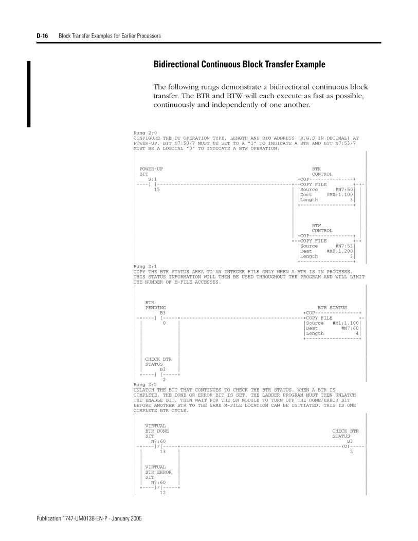
D-16 Block Transfer Examples for Earlier Processors
Bidirectional Continuous Block Transfer Example
The following rungs demonstrate a bidirectional continuous block transfer. The BTR and BTW will each execute as fast as possible, continuously and independently of one another.
Rung 2:0 CONFIGURE THE BT OPERATION TYPE, LENGTH AND RIO ADDRESS (R,G,S IN DECIMAL) AT POWER-UP. BIT N7:50/7 MUST BE SET TO A ”1” TO INDICATE A BTR AND BIT N7:53/7 MUST BE A LOGICAL ”0” TO INDICATE A BTW OPERATION. | | | | | | | POWER-UP BTR | | BIT CONTROL | | S:1 +COP---------------+ | |----] [----------------------------------------------+-+COPY FILE +-+-| | 15 | |Source #N7:50| | | | | |Dest #M0:1.100| | | | | |Length 3| | | | | +------------------+ | | | | | | | | | | | | | | | | BTW | | | | CONTROL | | | | +COP---------------+ | | | +-+COPY FILE +-+ | | |Source #N7:53| | | |Dest #M0:1.200| | | |Length 3| | | +------------------+ | Rung 2:1 COPY THE BTR STATUS AREA TO AN INTEGER FILE ONLY WHEN A BTR IS IN PROGRESS. THIS STATUS INFORMATION WILL THEN BE USED THROUGHOUT THE PROGRAM AND WILL LIMIT THE NUMBER OF M-FILE ACCESSES. | | | | | | | BTR | | PENDING BTR STATUS | | B3 +COP---------------+ | |-+----] [-----+------------------------------------------+COPY FILE +-| | | 0 | |Source #M1:1.100| | | | | |Dest #N7:60| | | | | |Length 4| | | | | +------------------+ | | | | | | | | | | | | | | | CHECK BTR | | | | STATUS | | | | B3 | | | +----] [-----+ | | 2 | Rung 2:2 UNLATCH THE BIT THAT CONTINUES TO CHECK THE BTR STATUS. WHEN A BTR IS COMPLETE, THE DONE OR ERROR BIT IS SET. THE LADDER PROGRAM MUST THEN UNLATCH THE ENABLE BIT, THEN WAIT FOR THE SN MODULE TO TURN OFF THE DONE/ERROR BIT BEFORE ANOTHER BTR TO THE SAME M-FILE LOCATION CAN BE INITIATED. THIS IS ONE COMPLETE BTR CYCLE. | | | | | VIRTUAL | | BTR DONE CHECK BTR | | BIT STATUS | | N7:60 B3 | |-+----]/[-----+-------------------------------------------------------(U)-----| | | 13 | 2 | | | | | | | | | | | VIRTUAL | | | | BTR ERROR | | | | BIT | | | | N7:60 | | | +----]/[-----+ | | 12 |
Publication 1747-UM013B-EN-P - January 2005

Block Transfer Examples for Earlier Processors D-17
Rung 2:3 COPY THE BTW STATUS AREA TO AN INTEGER FILE ONLY WHEN A BTW IS IN PROGRESS. THIS STATUS DATA WILL THEN BE USED THROUGHOUT THE PROGRAM AND WILL LIMIT THE NUMBER OF M-FILE ACCESSES. | | | | | | | BTW BTW | | PENDING STATUS | | B3 +COP---------------+ | |-+----] [-----+------------------------------------------+COPY FILE +-| | | 1 | |Source #M1:1.200| | | | | |Dest #N7:64| | | | | |Length 4| | | | | +------------------+ | | | | | | | | | | | | | | | CHECK BTW | | | | STATUS | | | | B3 | | | +----] [-----+ | | 3 | Rung 2:4 UNLATCH THE BIT THAT CONTINUES TO CHECK THE BTW STATUS. WHEN A BTW IS COMPLETE, THE DONE OR ERROR BIT IS SET. THE LADDER PROGRAM MUST THEN UNLATCH THE ENABLE BIT, THEN WAIT FOR THE SN MODULE TO TURN OFF THE THE DONE/ERROR BIT BEFORE ANOTHER BTW TO THE SAME M-FILE LOCATION CAN BE INITIATED. THIS COMPLETES ONE BTW CYCLE. | | | | | VIRTUAL | | BTW DONE CHECK BTW | | BIT STATUS | | N7:64 B3 | |-+----]/[-----+-------------------------------------------------------(U)-----| | | 13 | 3 | | | | | | | | | | | VIRTUAL | | | | BTW ERROR | | | | BIT | | | | N7:64 | | | +----]/[-----+ | | 12 |
Publication 1747-UM013B-EN-P - January 2005

D-18 Block Transfer Examples for Earlier Processors
Rung 2:5 WHEN A BTR SUCCESSFULLY COMPLETES, BUFFER THE BTR DATA AND UNLATCH BOTH THE BTR VIRTUAL ENABLE BIT AND THE BTR PENDING BIT. ALSO, LATCH THE BIT THAT CONTINUES CHECKING THE BTR STATUS UNTIL THE SN MODULE TURNS OFF THE DONE BIT. | | | | | VIRTUAL | | BTR DONE | | BIT BTR DATA | | N7:60 +COP---------------+ | |----] [----------------------------------------------+-+COPY FILE +-+-| | 13 | |Source #M1:1.110| | | | | |Dest #N7:0| | | | | |Length 10| | | | | +------------------+ | | | | | | | | | | | | | | | | BTR | | | | PENDING | | | | B3 | | | +----(U)---------------+ | | | 0 | | | | | | | | | | | | VIRTUAL | | | | BTR ENABLE | | | | BIT | | | | N7:50 | | | +----(U)---------------+ | | | 15 | | | | | |
|
| | | | | | | | | | | | | | | | | CHECK BTR | | | | STATUS | | | | B3 | | | +----(L)---------------+ | | 2 | Rung 2:6 WHEN A BTR UNSUCCESSFULLY COMPLETES, BUFFER THE ERROR CODE AND UNLATCH THE BTR ENABLE BIT AND THE BTR PENDING BIT. ALSO, LATCH THE CHECK BTR STATUS BIT IN ORDER TO CONTINUE READING THE STATUS INFORMATION FROM THE SCANNER UNTIL IT TURNS OFF THE ERROR BIT, COMPLETING THE HAND-SHAKE PROCESS. | | | | | VIRTUAL | | BTR ERROR BTR ERROR | | BIT CODE | | N7:60 +MOV---------------+ | |----] [----------------------------------------------+-+MOVE +-+-| | 12 | |Source M1:1.103| | | | | | *| | | | | |Dest N7:0| | | | | | 0| | | | | +------------------+ | | | | | | | | | | | | | | | | BTR | | | | PENDING | | | | B3 | | | +----(U)---------------+ | | | 0 | | | | | | | | | | | | VIRTUAL | | | | BTR ENABLE | | | | BIT | | | | N7:50 | | | +----(U)---------------+ | | | 15 | | | | | | | | | | | | | | | | CHECK BTR | | | | STATUS | | | | B3 | | | +----(L)---------------+ | | 2 |
Publication 1747-UM013B-EN-P - January 2005
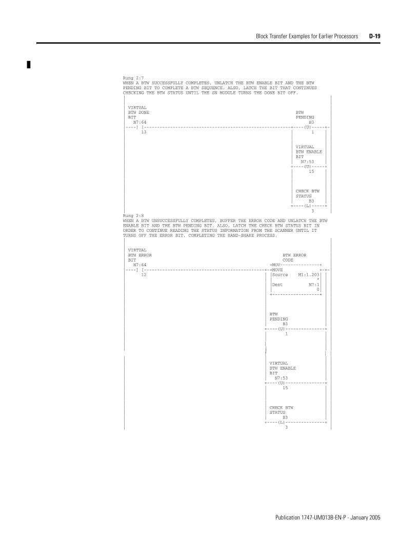
Block Transfer Examples for Earlier Processors D-19
Rung 2:7 WHEN A BTW SUCCESSFULLY COMPLETES, UNLATCH THE BTW ENABLE BIT AND THE BTW PENDING BIT TO COMPLETE A BTW SEQUENCE. ALSO, LATCH THE BIT THAT CONTINUES CHECKING THE BTW STATUS UNTIL THE SN MODULE TURNS THE DONE BIT OFF. | | | | | VIRTUAL | | BTW DONE BTW | | BIT PENDING | | N7:64 B3 | |----] [--------------------------------------------------------+----(U)-----+-| | 13 | 1 | | | | | | | | | | | | VIRTUAL | | | | BTW ENABLE | | | | BIT | | | | N7:53 | | | +----(U)-----+ | | | 15 | | | | | | | | | | | | | | | | CHECK BTW | | | | STATUS | | | | B3 | | | +----(L)-----+ | | 3 | Rung 2:8 WHEN A BTW UNSUCCESSFULLY COMPLETES, BUFFER THE ERROR CODE AND UNLATCH THE BTW ENABLE BIT AND THE BTW PENDING BIT. ALSO, LATCH THE CHECK BTW STATUS BIT IN ORDER TO CONTINUE READING THE STATUS INFORMATION FROM THE SCANNER UNTIL IT TURNS OFF THE ERROR BIT, COMPLETING THE HAND-SHAKE PROCESS. | | | | | VIRTUAL | | BTW ERROR BTW ERROR | | BIT CODE | | N7:64 +MOV---------------+ | |----] [----------------------------------------------+-+MOVE +-+-| | 12 | |Source M1:1.203| | | | | | *| | | | | |Dest N7:1| | | | | | 0| | | | | +------------------+ | | | | | | | | | | | | | | | | BTW | | | | PENDING | | | | B3 | | | +----(U)---------------+ | | | 1 | | | | | | | | | |
|
| | |
| | | |
| | | | | | VIRTUAL | | | | BTW ENABLE | | | | BIT | | | | N7:53 | | | +----(U)---------------+ | | | 15 | | | | | | | | | | | | | | | | CHECK BTW | | | | STATUS | | | | B3 | | | +----(L)---------------+ | | 3 |
Publication 1747-UM013B-EN-P - January 2005

D-20 Block Transfer Examples for Earlier Processors
Rung 2:9 THIS RUNG WILL EXECUTE BLOCK TRANSFER READS CONTINUOUSLY, AS FAST AS POSSIBLE. | | | | | | | | | VIRTUAL |VIRTUAL |VIRTUAL | | BTR ENABLE|BTR DONE |BTR ERROR BTR | | BIT |BIT |BIT PENDING | | N7:50 N7:60 N7:60 B3 | |----]/[--------]/[--------]/[----------------------------------+----(L)-----+-| | 15 13 12 | 0 | | | | | | | | | | | | VIRTUAL | | | | BTR ENABLE | | | | BIT | | | | N7:50 | | | +----(L)-----+ | | 15 | Rung 2:10 THIS RUNG WILL EXECUTE BLOCK TRANSFER WRITES CONTINUOUSLY, AS FAST AS POSSIBLE. | | | | | | | | | VIRTUAL |VIRTUAL |VIRTUAL | | BTW ENABLE|BTW DONE |BTW ERROR | | BIT |BIT |BIT BTW DATA | | N7:53 N7:64 N7:64 +COP---------------+ | |----]/[--------]/[--------]/[------------------------+-+COPY FILE +-+-| | 15 13 12 | |Source #N7:10| | | | | |Dest #M0:1.210| | | | | |Length 11| | | | | +------------------+ | | | | | | | | | | |
| | | | | | | | | | | | | VIRTUAL | | | | BTW ENABLE | | | | BIT | | | | N7:53 | | | +----(L)---------------+ | | | 15 | | | | | | | | | | | | | | | | BTW | | | | PENDING | | | | B3 | | | +----(L)---------------+ | | 1 | Rung 2:11 MOVE THE VIRTUAL BTR CONTROL WORD TO THE M0 FILE FOR THE SN MODULE WHILE A BTR IS IN PROGRESS, AND CONTINUE DOING SO UNTIL THE ENABLE, DONE AND ERROR BITS ARE ALL TURNED OFF, COMPLETING THE HAND-SHAKE PROCESS. | | | | | VIRTUAL BTR | | BTR ENABLE CONTROL | | BIT BITS | | N7:50 +MOV---------------+ | |-+----] [-----+------------------------------------------+MOVE +-| | | 15 | |Source N7:50| | | | | | 0| | | | | |Dest M0:1.100| | | | | | *| | | | | +------------------+ | | | | | | | | | | | VIRTUAL | | | | BTR DONE | | | | BIT | | | | N7:60 | | | +----] [-----+ | | | 13 | | | | | | | | | | | | VIRTUAL | | | | BTR ERROR | | | | BIT | | | | N7:60 | | | +----] [-----+ | | 12 |
Publication 1747-UM013B-EN-P - January 2005

Block Transfer Examples for Earlier Processors D-21
Bidirectional Alternating Block Transfer
The following rungs demonstrate a bidirectional alternating block transfer. Using these rungs ensures the block transfer requests are executed in the order in which they are sent to the queue. This example also ensures that the block transfer read and block transfer write alternate. The XIO conditions prevent the BTR and BTW from queueing simultaneously. The block transfers continue as long as the XIC precondition bit is true.
Rung 2:12 MOVE THE VIRTUAL BTW CONTROL WORD TO THE M0 FILE FOR THE SN MODULE WHILE A BTW IS IN PROGRESS, AND CONTINUE DOING SO UNTIL THE ENABLE, DONE AND ERROR BITS ARE ALL TURNED OFF, COMPLETING THE HAND-SHAKE PROCESS. | | | | | VIRTUAL BTW | | BTW ENABLE CONTROL | | BIT BITS | | N7:53 +MOV---------------+ | |-+----] [-----+------------------------------------------+MOVE +-| | | 15 | |Source N7:53| | | | | | 0| | | | | |Dest M0:1.200| | | | | | *| | | | | +------------------+ | | | | | | | | | | | VIRTUAL | | | | BTW DONE | | | | BIT | | | | N7:64 | | | +----] [-----+ | | | 13 | | | | | | | | | | | | VIRTUAL | | | | BTW ERROR | | | | BIT | | | | N7:64 | | | +----] [-----+ | | 12 | Rung 2:13 | | |-------------------------------------+END+------------------------------------| | |
Publication 1747-UM013B-EN-P - January 2005
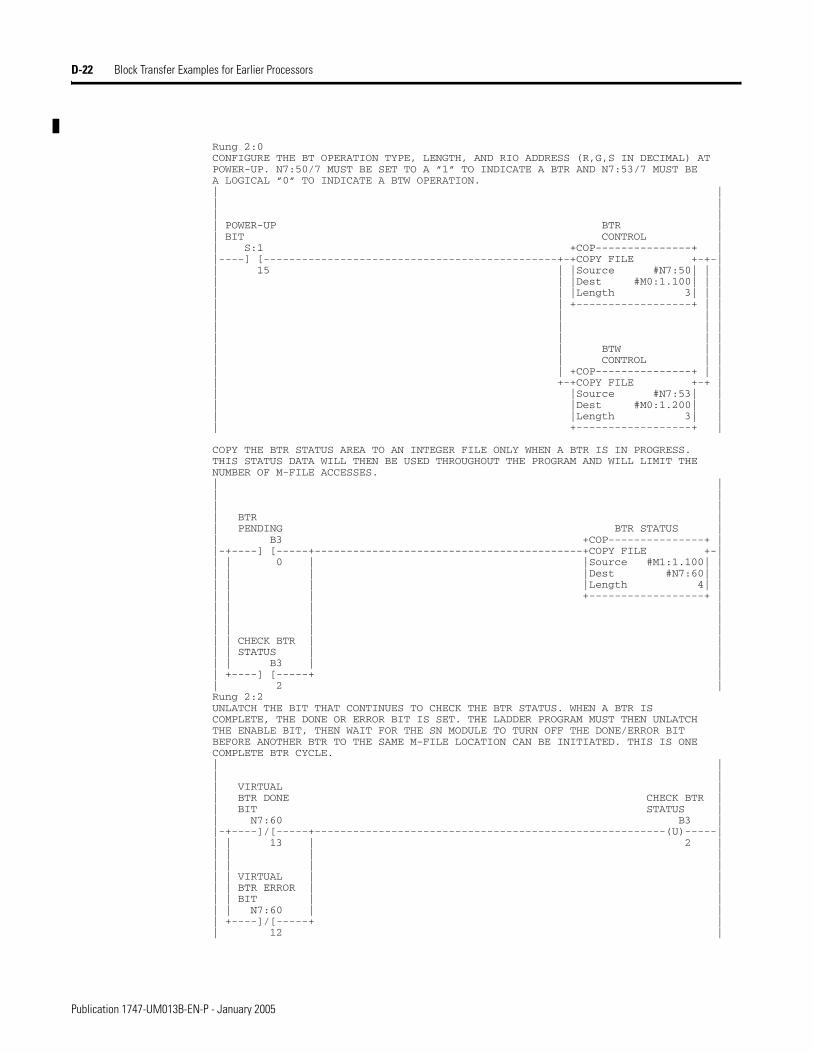
D-22 Block Transfer Examples for Earlier Processors
Rung 2:0 CONFIGURE THE BT OPERATION TYPE, LENGTH, AND RIO ADDRESS (R,G,S IN DECIMAL) AT POWER-UP. N7:50/7 MUST BE SET TO A ”1” TO INDICATE A BTR AND N7:53/7 MUST BE A LOGICAL ”0” TO INDICATE A BTW OPERATION. | | | | | | | POWER-UP BTR | | BIT CONTROL | | S:1 +COP---------------+ | |----] [----------------------------------------------+-+COPY FILE +-+-| | 15 | |Source #N7:50| | | | | |Dest #M0:1.100| | | | | |Length 3| | | | | +------------------+ | | | | | | | | | | | | | | | | BTW | | | | CONTROL | | | | +COP---------------+ | | | +-+COPY FILE +-+ | | |Source #N7:53| | | |Dest #M0:1.200| | | |Length 3| | | +------------------+ | COPY THE BTR STATUS AREA TO AN INTEGER FILE ONLY WHEN A BTR IS IN PROGRESS. THIS STATUS DATA WILL THEN BE USED THROUGHOUT THE PROGRAM AND WILL LIMIT THE NUMBER OF M-FILE ACCESSES. | | | | | | | BTR | | PENDING BTR STATUS | | B3 +COP---------------+ | |-+----] [-----+------------------------------------------+COPY FILE +-| | | 0 | |Source #M1:1.100| | | | | |Dest #N7:60| | | | | |Length 4| | | | | +------------------+ | | | | | | | | | | | | | | | CHECK BTR | | | | STATUS | | | | B3 | | | +----] [-----+ | | 2 | Rung 2:2 UNLATCH THE BIT THAT CONTINUES TO CHECK THE BTR STATUS. WHEN A BTR IS COMPLETE, THE DONE OR ERROR BIT IS SET. THE LADDER PROGRAM MUST THEN UNLATCH THE ENABLE BIT, THEN WAIT FOR THE SN MODULE TO TURN OFF THE DONE/ERROR BIT BEFORE ANOTHER BTR TO THE SAME M-FILE LOCATION CAN BE INITIATED. THIS IS ONE COMPLETE BTR CYCLE. | | | | | VIRTUAL | | BTR DONE CHECK BTR | | BIT STATUS | | N7:60 B3 | |-+----]/[-----+-------------------------------------------------------(U)-----| | | 13 | 2 | | | | | | | | | | | VIRTUAL | | | | BTR ERROR | | | | BIT | | | | N7:60 | | | +----]/[-----+ | | 12 |
Publication 1747-UM013B-EN-P - January 2005
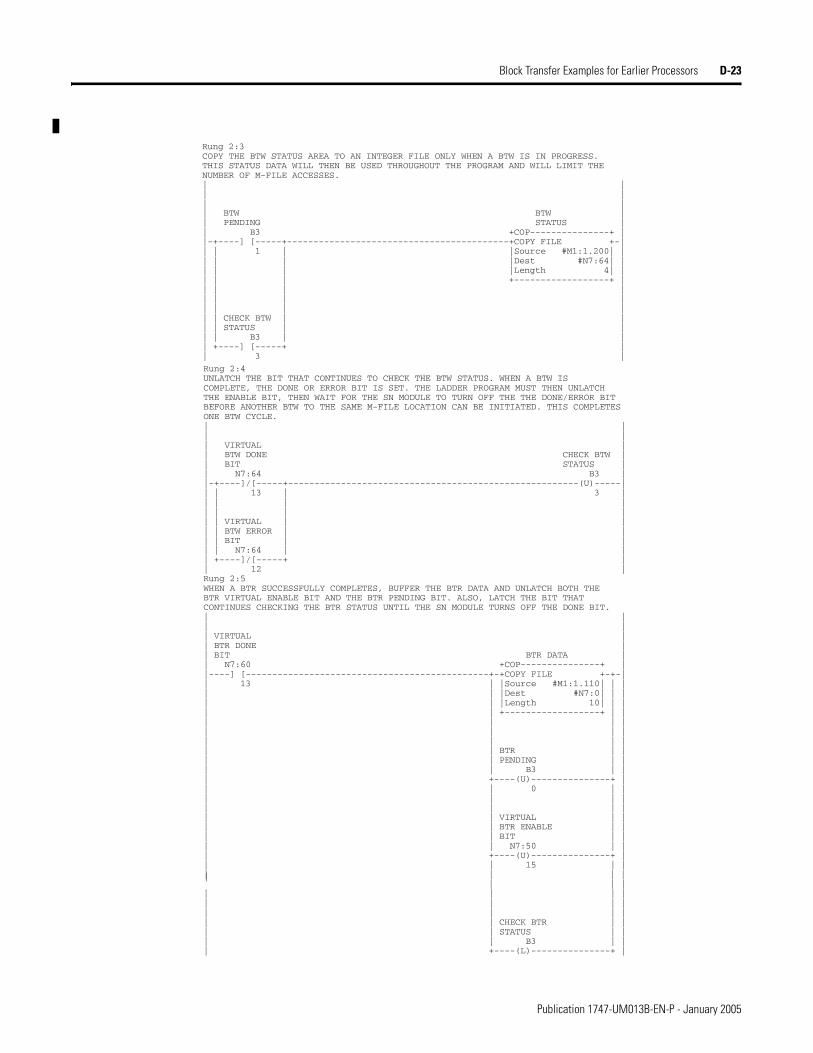
Block Transfer Examples for Earlier Processors D-23
| BTW BTW | | PENDING STATUS | | B3 +COP---------------+ | |-+----] [-----+------------------------------------------+COPY FILE +-| | | 1 | |Source #M1:1.200| | | | | |Dest #N7:64| | | | | |Length 4| | | | | +------------------+ | | | | | | | | | | | | | | | CHECK BTW | | | | STATUS | | | | B3 | | | +----] [-----+ | | 3 |
Rung 2:3 COPY THE BTW STATUS AREA TO AN INTEGER FILE ONLY WHEN A BTW IS IN PROGRESS. THIS STATUS DATA WILL THEN BE USED THROUGHOUT THE PROGRAM AND WILL LIMIT THE NUMBER OF M-FILE ACCESSES. | | | | | |
Rung 2:4 UNLATCH THE BIT THAT CONTINUES TO CHECK THE BTW STATUS. WHEN A BTW IS COMPLETE, THE DONE OR ERROR BIT IS SET. THE LADDER PROGRAM MUST THEN UNLATCH THE ENABLE BIT, THEN WAIT FOR THE SN MODULE TO TURN OFF THE THE DONE/ERROR BIT BEFORE ANOTHER BTW TO THE SAME M-FILE LOCATION CAN BE INITIATED. THIS COMPLETES ONE BTW CYCLE. | | | | | VIRTUAL | | BTW DONE CHECK BTW | | BIT STATUS | | N7:64 B3 | |-+----]/[-----+-------------------------------------------------------(U)-----| | | 13 | 3 | | | | | | | | | | | VIRTUAL | | | | BTW ERROR | | | | BIT | | | | N7:64 | | | +----]/[-----+ | | 12 | Rung 2:5 WHEN A BTR SUCCESSFULLY COMPLETES, BUFFER THE BTR DATA AND UNLATCH BOTH THE BTR VIRTUAL ENABLE BIT AND THE BTR PENDING BIT. ALSO, LATCH THE BIT THAT CONTINUES CHECKING THE BTR STATUS UNTIL THE SN MODULE TURNS OFF THE DONE BIT. | | | | | VIRTUAL | | BTR DONE | | BIT BTR DATA | | N7:60 +COP---------------+ | |----] [----------------------------------------------+-+COPY FILE +-+-| | 13 | |Source #M1:1.110| | | | | |Dest #N7:0| | | | | |Length 10| | | | | +------------------+ | | | | | | | | | | | | | | | | BTR | | | | PENDING | | | | B3 | | | +----(U)---------------+ | | | 0 | | | | | | | | | | | | VIRTUAL | | | | BTR ENABLE | | | | BIT | | | | N7:50 | | | +----(U)---------------+ | | | 15 | | | | | | |
| | | | | | | | | | | | | | | | | CHECK BTR | | | | STATUS | | | | B3 | | | +----(L)---------------+ |
Publication 1747-UM013B-EN-P - January 2005
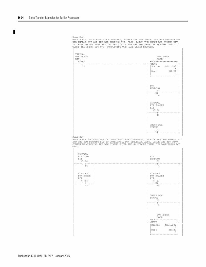
D-24 Block Transfer Examples for Earlier Processors
Rung 2:6 WHEN A BTR UNSUCCESSFULLY COMPLETES, BUFFER THE BTR ERROR CODE AND UNLATCH THE BTR ENABLE BIT AND THE BTR PENDING BIT. ALSO, LATCH THE CHECK BTR STATUS BIT IN ORDER TO CONTINUE READING THE STATUS INFORMATION FROM THE SCANNER UNTIL IT TURNS THE ERROR BIT OFF, COMPLETING THE HAND-SHAKE PROCESS. | | | | | VIRTUAL | | BTR ERROR BTR ERROR | | BIT CODE | | N7:60 +MOV---------------+ | |----] [----------------------------------------------+-+MOVE +-+-| | 12 | |Source M1:1.103| | | | | | *| | | | | |Dest N7:21| | | | | | 0| | | | | +------------------+ | | | | | | | | | | | | | | | | BTR | | | | PENDING | | | | B3 | | | +----(U)---------------+ | | | 0 | | | | | | | | | | | | VIRTUAL | | | | BTR ENABLE | | | | BIT | | | | N7:50 | | | +----(U)---------------+ | | | 15 | | | | | | | | | | | | | | | | CHECK BTR | | | | STATUS | | | | B3 | | | +----(L)---------------+ | | 2 | Rung 2:7 WHEN A BTW SUCCESSFULLY OR UNSUCCESSFULLY COMPLETES, UNLATCH THE BTW ENABLE BIT AND THE BTW PENDING BIT TO COMPLETE A BTW SEQUENCE. ALSO, LATCH THE BIT THAT CONTINUES CHECKING THE BTW STATUS UNTIL THE SN MODULE TURNS THE DONE/ERROR BIT OFF. | | | | | VIRTUAL | | BTW DONE BTW | | BIT PENDING | | N7:64 B3 | |-+----] [-----+--------------------------------------+----(U)---------------+-| | | 13 | | 1 | | | | | | | | | | | | | | | | VIRTUAL | | VIRTUAL | | | | BTW ERROR | | BTW ENABLE | | | | BIT | | BIT | | | | N7:64 | | N7:53 | | | +----] [-----+ +----(U)---------------+ | | 12 | 15 | | | | | | | | | | | | | | | | CHECK BTW | | | | STATUS | | | | B3 | | | +----(L)---------------+ | | | 3 | | | | | | | | | | | | | | | | BTW ERROR | | | | CODE | | | | +MOV---------------+ | | | +-+MOVE +-+ | | |Source M1:1.203| | | | *| | | |Dest N7:22| | | | 0| | | +------------------+ |
Publication 1747-UM013B-EN-P - January 2005
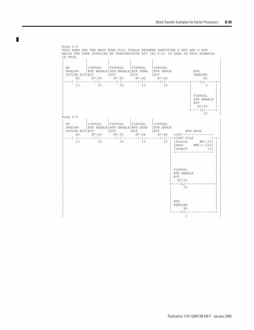
Block Transfer Examples for Earlier Processors D-25
Rung 2:8 THIS RUNG AND THE NEXT RUNG WILL TOGGLE BETWEEN EXECUTING A BTR AND A BTW WHILE THE USER SUPPLIED BT PRECONDITION BIT (B3:0/11 IS USED IN THIS EXAMPLE) IS TRUE. | | | | | | | | | | | | | BT |VIRTUAL |VIRTUAL |VIRTUAL |VIRTUAL | | PRECON- |BTR ENABLE|BTW ENABLE|BTR DONE |BTR ERROR BTR | | DITION BIT|BIT |BIT |BIT |BIT PENDING | | B3 N7:50 N7:53 N7:60 N7:60 B3 | |----] [--------]/[--------]/[--------]/[--------]/[------------+----(L)-----+-| | 11 15 15 13 12 | 0 | | | | | | | | | | | | VIRTUAL | | | | BTR ENABLE | | | | BIT | | | | N7:50 | | | +----(L)-----+ | | 15 | Rung 2:9 | | | | | | | BT |VIRTUAL |VIRTUAL |VIRTUAL |VIRTUAL | | PRECON- |BTR ENABLE|BTW ENABLE|BTW DONE |BTW ERROR | | DITION BIT|BIT |BIT |BIT |BIT BTW DATA | | B3 N7:50 N7:53 N7:64 N7:64 +COP---------------+ | |----] [--------]/[--------]/[--------]/[--------]/[|-+-+COPY FILE +-+-| | 11 15 15 13 12 | |Source #N7:10| | | | | |Dest #M0:1.210| | | | | |Length 11| | | | | +------------------+ | | | | | | | | | | | | | | | | | | | | VIRTUAL | | | | BTW ENABLE | | | | BIT | | | | N7:53 | | | +----(L)---------------+ | | | 15 | | | | | | | | | | | | | | | | BTW | | | | PENDING | | | | B3 | | | +----(L)---------------+ | | 1 |
Publication 1747-UM013B-EN-P - January 2005
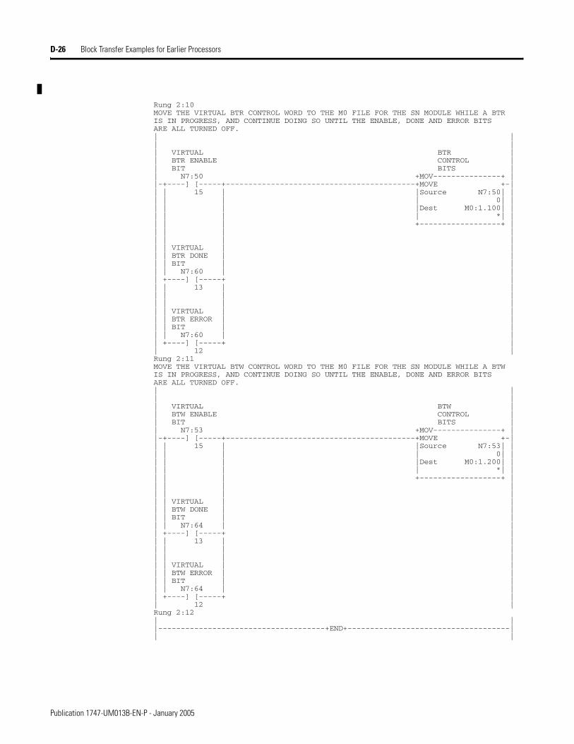
D-26 Block Transfer Examples for Earlier Processors
Rung 2:10 MOVE THE VIRTUAL BTR CONTROL WORD TO THE M0 FILE FOR THE SN MODULE WHILE A BTR IS IN PROGRESS, AND CONTINUE DOING SO UNTIL THE ENABLE, DONE AND ERROR BITS ARE ALL TURNED OFF. | | | | | VIRTUAL BTR | | BTR ENABLE CONTROL | | BIT BITS | | N7:50 +MOV---------------+ | |-+----] [-----+------------------------------------------+MOVE +-| | | 15 | |Source N7:50| | | | | | 0| | | | | |Dest M0:1.100| | | | | | *| | | | | +------------------+ | | | | | | | | | | | VIRTUAL | | | | BTR DONE | | | | BIT | | | | N7:60 | | | +----] [-----+ | | | 13 | | | | | | | | | | | | VIRTUAL | | | | BTR ERROR | | | | BIT | | | | N7:60 | | | +----] [-----+ | | 12 | Rung 2:11 MOVE THE VIRTUAL BTW CONTROL WORD TO THE M0 FILE FOR THE SN MODULE WHILE A BTW IS IN PROGRESS, AND CONTINUE DOING SO UNTIL THE ENABLE, DONE AND ERROR BITS ARE ALL TURNED OFF. | | | | | VIRTUAL BTW | | BTW ENABLE CONTROL | | BIT BITS | | N7:53 +MOV---------------+ | |-+----] [-----+------------------------------------------+MOVE +-| | | 15 | |Source N7:53| | | | | | 0| | | | | |Dest M0:1.200| | | | | | *| | | | | +------------------+ | | | | | | | | | | | VIRTUAL | | | | BTW DONE | | | | BIT | | | | N7:64 | | | +----] [-----+ | | | 13 | | | | | | | | | | | | VIRTUAL | | | | BTW ERROR | | | | BIT | | | | N7:64 | | | +----] [-----+ | | 12 | Rung 2:12 | | |-------------------------------------+END+------------------------------------| | |
Publication 1747-UM013B-EN-P - January 2005
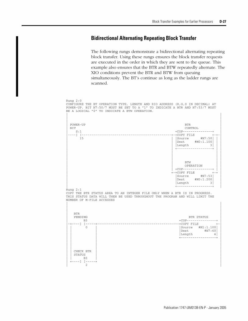
Block Transfer Examples for Earlier Processors D-27
Bidirectional Alternating Repeating Block Transfer
The following rungs demonstrate a bidirectional alternating repeating block transfer. Using these rungs ensures the block transfer requests are executed in the order in which they are sent to the queue. This example also ensures that the BTR and BTW repeatedly alternate. The XIO conditions prevent the BTR and BTW from queuing simultaneously. The BT’s continue as long as the ladder rungs are scanned.
Rung 2:0 CONFIGURE THE BT OPERATION TYPE, LENGTH AND RIO ADDRESS (R,G,S IN DECIMAL) AT POWER-UP. BIT N7:50/7 MUST BE SET TO A ”1” TO INDICATE A BTR AND N7:53/7 MUST BE A LOGICAL ”0” TO INDICATE A BTW OPERATION. | | | | | | | POWER-UP BTR | | BIT CONTROL | | S:1 +COP---------------+ | |----] [----------------------------------------------+-+COPY FILE +-+-| | 15 | |Source #N7:50| | | | | |Dest #M0:1.100| | | | | |Length 3| | | | | +------------------+ | | | | | | | | | | | | | | | | BTW | | | | OPERATION | | | | +COP---------------+ | | | +-+COPY FILE +-+ | | |Source #N7:53| | | |Dest #M0:1.200| | | |Length 3| | | +------------------+ | Rung 2:1 COPY THE BTR STATUS AREA TO AN INTEGER FILE ONLY WHEN A BTR IS IN PROGRESS. THIS STATUS DATA WILL THEN BE USED THROUGHOUT THE PROGRAM AND WILL LIMIT THE NUMBER OF M-FILE ACCESSES | | | | | | | BTR | | PENDING BTR STATUS | | B3 +COP---------------+ | |-+----] [-----+------------------------------------------+COPY FILE +-| | | 0 | |Source #M1:1.100| | | | | |Dest #N7:60| | | | | |Length 4| | | | | +------------------+ | | | | | | | | | | | | | | | CHECK BTR | | | | STATUS | | | | B3 | | | +----] [-----+ | | 2 |
Publication 1747-UM013B-EN-P - January 2005

D-28 Block Transfer Examples for Earlier Processors
Rung 2:2 UNLATCH THE BIT THAT CONTINUES TO CHECK THE BTR STATUS. WHEN A BTR IS COMPLETE, THE DONE OR ERROR BIT IS SET. THE LADDER PROGRAM MUST THEN UNLATCH THE ENABLE BIT, THEN WAIT FOR THE SN MODULE TO TURN OFF THE DONE/ERROR BIT BEFORE ANOTHER BTR TO THE SAME M-FILE LOCATION CAN BE INITIATED. THIS IS ONE COMPLETE BTR CYCLE. | | | | | VIRTUAL | | BTR DONE CHECK BTR | | BIT STATUS | | N7:60 B3 | |-+----]/[-----+-------------------------------------------------------(U)-----| | | 13 | 2 | | | | | | | | | | | | | | | BTR ERROR | |
BIT | | | | N7:60 | | | +----]/[-----+ | | 12 | Rung 2:3 COPY THE BTW STATUS AREA TO AN INTEGER FILE ONLY WHEN A BTW IS IN PROGRESS. THIS STATUS DATA WILL THEN BE USED THROUGHOUT THE PROGRAM AND WILL LIMIT THE NUMBER OF M-FILE ACCESSES. | | | | | | | BTW BTW | | PENDING STATUS | | B3 +COP---------------+ | |-+----] [-----+------------------------------------------+COPY FILE +-| | | 1 | |Source #M1:1.200| | | | | |Dest #N7:64| | | | | |Length 4| | | | | +------------------+ | | | | | | | | | | | | | | | CHECK BTW | | | | STATUS | | | | B3 | | | +----] [-----+ | | 3 | Rung 2:4 UNLATCH THE BIT THAT CONTINUES TO CHECK THE BTW STATUS. WHEN A BTW IS COMPLETE, THE DONE OR ERROR BIT IS SET. THE LADDER PROGRAM MUST THEN UNLATCH THE ENABLE BIT, THEN WAIT FOR THE SN MODULE TO TURN OFF THE THE DONE/ERROR BIT BEFORE ANOTHER BTW TO THE SAME M-FILE LOCATION CAN BE INITIATED. THIS COMPLETES ONE BTW CYCLE. | | | | | VIRTUAL | | BTW DONE CHECK BTW | | BIT STATUS | | N7:64 B3 | |-+----]/[-----+-------------------------------------------------------(U)-----| | | 13 | 3 | | | | | | | | | | | VIRTUAL | | | | BTW ERROR | | | | BIT | | | | N7:64 | | | +----]/[-----+ | | 12 |
Publication 1747-UM013B-EN-P - January 2005

Block Transfer Examples for Earlier Processors D-29
Rung 2:5 WHEN A BTR SUCCESSFULLY COMPLETES, BUFFER THE BTR DATA AND UNLATCH BOTH THE BTR VIRTUAL ENABLE BIT AND THE BTR PENDING BIT. ALSO, LATCH THE BIT THAT CONTINUES CHECKING THE BTR STATUS UNTIL THE SN MODULE TURNS OFF THE DONE BIT. | | | | | VIRTUAL | | BTR DONE | | BIT BTR DATA | | N7:60 +COP---------------+ | |----] [----------------------------------------------+-+COPY FILE +-+-| | 13 | |Source #M1:1.110| | | | | |Dest #N7:0| | | | | |Length 10| | | | | +------------------+ | | | | | | | | | | | | | | | | BTR | | | | PENDING | | | | B3 | | | +----(U)---------------+ | | | 0 | | | | | | | | | | | | VIRTUAL | | | | BTR ENABLE | | | | BIT | | | | N7:50 | | | +----(U)---------------+ | | | 15 | | | | | |
| | | | | | | | | | | | | | | | | | CHECK BTR | | | | STATUS | | | | B3 | | | +----(L)---------------+ | | 2 | Rung 2:6 WHEN A BTR UNSUCCESSFULLY COMPLETES, BUFFER THE ERROR CODE AND UNLATCH THE BTR ENABLE BIT AND THE BTR PENDING BIT. ALSO, LATCH THE CHECK BTR STATUS BIT IN ORDER TO CONTINUE READING THE STATUS INFORMATION FROM THE SCANNER UNTIL IT TURNS THE ERROR BIT OFF, COMPLETING THE HAND-SHAKE PROCESS. | | | | | BTR ERROR | | BIT | | N7:60 +MOV---------------+ | |----] [----------------------------------------------+-+MOVE +-+-| | 12 | |Source M1:1.103| | | | | | *| | | | | |Dest N7:21| | | | | | 0| | | | | +------------------+ | | | | | | | | | | | | | | | | BTR | | | | PENDING | | | | B3 | | | +----(U)---------------+ | | | 0 | | | | | | | | | | | | VIRTUAL | | | | BTR ENABLE | | | | BIT | | | | N7:50 | | | +----(U)---------------+ | | | 15 | | | | | | | | | | | | | | | | CHECK BTR | | | | STATUS | | | | B3 | | | +----(L)---------------+ | | 2 |
Publication 1747-UM013B-EN-P - January 2005
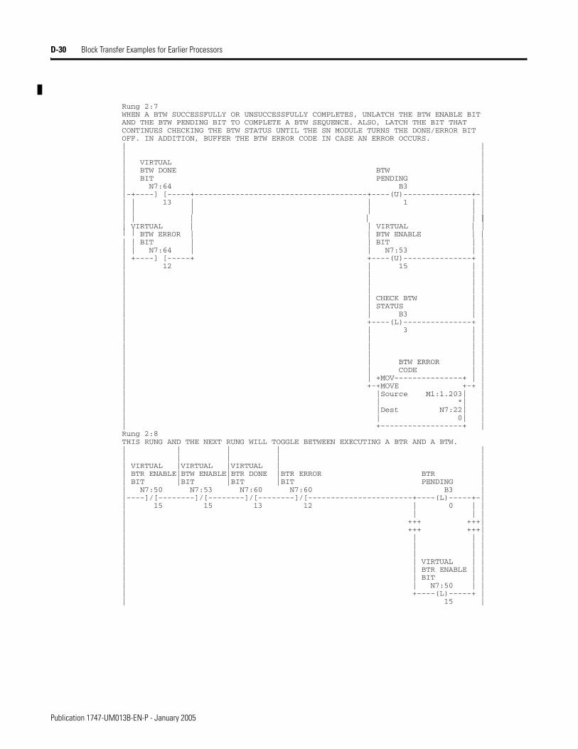
D-30 Block Transfer Examples for Earlier Processors
Rung 2:7 WHEN A BTW SUCCESSFULLY OR UNSUCCESSFULLY COMPLETES, UNLATCH THE BTW ENABLE BIT AND THE BTW PENDING BIT TO COMPLETE A BTW SEQUENCE. ALSO, LATCH THE BIT THAT CONTINUES CHECKING THE BTW STATUS UNTIL THE SN MODULE TURNS THE DONE/ERROR BIT OFF. IN ADDITION, BUFFER THE BTW ERROR CODE IN CASE AN ERROR OCCURS. | | | | | VIRTUAL | | BTW DONE BTW | | BIT PENDING | | N7:64 B3 | |-+----] [-----+--------------------------------------+----(U)---------------+-| | | 13 | | 1 | | | | | | | | | | | | | | | | VIRTUAL | | VIRTUAL | |
| | BTW ERROR | | BTW ENABLE | |
| | BIT | | BIT | | | | N7:64 | | N7:53 | | | +----] [-----+ +----(U)---------------+ | | 12 | 15 | | | | | | | | | | | | | | | | CHECK BTW | | | | STATUS | | | | B3 | | | +----(L)---------------+ | | | 3 | | | | | | | | | | | | | | | | BTW ERROR | | | | CODE | | | | +MOV---------------+ | | | +-+MOVE +-+ | | |Source M1:1.203| | | | *| | | |Dest N7:22| | | | 0| | | +------------------+ | Rung 2:8 THIS RUNG AND THE NEXT RUNG WILL TOGGLE BETWEEN EXECUTING A BTR AND A BTW. | | | | | | | | | | | VIRTUAL |VIRTUAL |VIRTUAL | | | BTR ENABLE|BTW ENABLE|BTR DONE |BTR ERROR BTR | | BIT |BIT |BIT |BIT PENDING | | N7:50 N7:53 N7:60 N7:60 B3 | |----]/[--------]/[--------]/[--------]/[-----------------------+----(L)-----+-| | 15 15 13 12 | 0 | | | | | | | +++ +++| | +++ +++| | | | | | | | | | | | | | | VIRTUAL | | | | BTR ENABLE | | | | BIT | | | | N7:50 | | | +----(L)-----+ | | 15 |
Publication 1747-UM013B-EN-P - January 2005
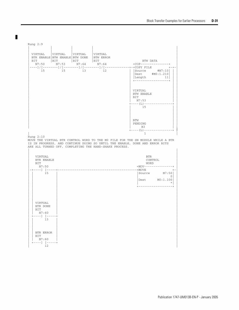
Block Transfer Examples for Earlier Processors D-31
Rung 2:9 | | | | | | | | | | | VIRTUAL |VIRTUAL |VIRTUAL |VIRTUAL | | BTR ENABLE|BTW ENABLE|BTW DONE |BTW ERROR | | BIT |BIT |BIT |BIT BTW DATA | | N7:50 N7:53 N7:64 N7:64 +COP---------------+ | |----]/[--------]/[--------]/[--------]/[-------------+-+COPY FILE +-+-| | 15 15 13 12 | |Source #N7:10| | | | | |Dest #M0:1.210| | | | | |Length 11| | | | | +------------------+ | | | | | | | | | | | | VIRTUAL | | | | BTW ENABLE | | | | BIT | | | | N7:53 | | | +----(L)---------------+ | | | 15 | | | | | | | | | | | | | | | | BTW | | | | PENDING | | | | B3 | |
|
+----(L)---------------+ | | 1 | Rung 2:10 MOVE THE VIRTUAL BTR CONTROL WORD TO THE M0 FILE FOR THE SN MODULE WHILE A BTR IS IN PROGRESS, AND CONTINUE DOING SO UNTIL THE ENABLE, DONE AND ERROR BITS ARE ALL TURNED OFF, COMPLETING THE HAND-SHAKE PROCESS. | | | | | VIRTUAL BTR | | BTR ENABLE CONTROL | | BIT WORD | | N7:50 +MOV---------------+ | |-+----] [-----+------------------------------------------+MOVE +-| | | 15 | |Source N7:50| | | | | | 0| | | | | |Dest M0:1.100| | | | | | *| | | | | +------------------+ | | | | | | | | | | | | | | | | | | | VIRTUAL | | | | BTR DONE | | | | BIT | | | | N7:60 | | | +----] [-----+ | | | 13 | | | | | | | | | | | | | | | | BTR ERROR | | | | BIT | | | | N7:60 | | | +----] [-----+ | | 12 |
Publication 1747-UM013B-EN-P - January 2005

D-32 Block Transfer Examples for Earlier Processors
Rung 2:11 MOVE THE VIRTUAL BTW CONTROL WORD TO THE M0 FILE FOR THE SN MODULE WHILE A BTR IS IN PROGRESS, AND CONTINUE DOING SO UNTIL THE ENABLE, DONE AND ERROR BITS ARE ALL TURNED OFF, COMPLETING THE HAND-SHAKE PROCESS. | | | | | VIRTUAL BTW | | BTW ENABLE CONTROL | | BIT WORD | | N7:53
+MOV---------------+ |
|-+----] [-----+------------------------------------------+MOVE +-| | | 15 | |Source N7:53| | | | | | 0| | | | | |Dest M0:1.200| | | | | | *| | | | | +------------------+ | | | | | | | | | | | VIRTUAL | | | | BTW DONE | | | | BIT | | | | N7:64 | | | +----] [-----+ | | | 13 | | | | | | | | | | | | VIRTUAL | | | | BTW ERROR | | | | BIT | | | | N7:64 | | | +----] [-----+ | | 12 | Rung 2:12 | | |-------------------------------------+END+------------------------------------| | |
Publication 1747-UM013B-EN-P - January 2005

Glossary
The following terms are used throughout this manual. Refer to the Allen-Bradley Industrial Automation Glossary, Publication Number AG-7.1, for a complete guide to Allen-Bradley technical terms.
Adapter
Any physical device that is a slave on the RIO link.
Adapter Image
That portion of the scanner image assigned to an individual adapter.
ASB Module
The Catalog Number 1747-ASB, 1771-ASB, or 1794 - ASB Remote I/O Adapter Module. The ASB module is an adapter.
ASB Module Chassis
The chassis directly controlled by the ASB module. This includes the remote chassis and (if installed) two remote expansion chassis when using the 1747-ASB.
Block Transfer (BT)
See RIO Block Transfer.
Block Transfer Read (BTR)
A form of block transfer that occurs when a remote device transfers data to the SLC processor.
Block Transfer Write (BTW)
A form of block transfer that occurs when the SLC processor transfers data to a remote device.
Complementary I/O
Functionality that allows you to maximize I/O usage by pairing up I/O data from a primary and complementary chassis.
Discrete I/O
An input or output device that has corresponding bit locations in the scanner’s input or output file.
Discrete I/O Module
An I/O module used to sense or control two-state (ON/OFF) devices.
1 Publication 1747-UM013B-EN-P - January 2005
Glossary 2
Extended Node Capability
Functionality that allows you to use an 82 Ohm termination resistor at both ends of the RIO link for all baud rates. This functionality also allows for up to 32 adapters to be connected to the RIO link.
G file
The SLC file used to configure the scanner. You enter configuration information into this file during SLC processor programming. This file is loaded to the scanner by the SLC processor upon entering run mode.
Inhibit
A function by which the scanner stops communicating with a logical device. The logical device will consider itself inhibited if it does not receive communications from the scanner within a certain period of time.
Input file
The scanner’s input image file that is updated during the SLC processor input scan.
Local Expansion Chassis
A chassis that is connected to a local SLC chassis using a 1747-C9 (91.4 cm [36 in.]) or 1747-C7 (15.2 cm [6 in.]) cable.
Local SLC Chassis
The chassis that contains the SLC processor and scanner.
Logical Device
Any portion of a logical rack that is assigned to a single adapter. Adapters may appear as more than one logical device.
Logical Group
A logical group consists of one input and one output word within a logical rack. A word consists of 16 bits, each bit represents one terminal on a discrete I/O module.
Logical Rack
A fixed section of the scanner image comprised of eight input image words and eight output image words.
Publication 1747-UM013B-EN-P - January 2005
Glossary 3
Logical Slot
A logical slot consists of one input and one output byte within a logical group. A byte consists of 8 bits, each bit represents one terminal on a discrete I/O module.
M files
The SLC M0 and M1 data files that reside in the scanner. M files contain RIO network status (M1) and control (M0) information. The contents of these files can be directly accessed by your application program. Also, the M files are used to control and monitor RIO block transfer operations.
Output file
The scanner’s output file that is updated during the SLC processor output scan.
Remote Chassis
The chassis containing an ASB module and connected to the local SLC chassis via the RIO link.
Remote Expansion Chassis
A chassis that is connected to a remote chassis using a 1747-C9 (91.4 cm [36 in.]) or 1747-C7 (15.2 cm [6 in.]) cable.
Reset, Adapter Decide
Commands sent by the scanner to a logical device during an RIO discrete transfer. These commands instruct the logical device to reset all of its discrete outputs if hold last state is not selected, or to hold all of its discrete outputs in their last state if hold last state is selected.
Reset, Adapter Reset
Commands sent by the scanner to a logical device during an RIO discrete transfer. These commands instruct the logical device to reset all of its discrete outputs, regardless of the hold last state selection.
RIO Block Transfer
The exchange of up to 64 words of data between the scanner and a remote device. RIO block transfers only occur if you program them in your processor control program.
Publication 1747-UM013B-EN-P - January 2005
Glossary 4
RIO Discrete Transfer
The exchange of image data between the scanner and adapter. RIO discrete transfers occur continuously whenever the scanner and adapter are communicating on the RIO link.
RIO Link
An Allen-Bradley communication system supporting high-speed serial transfer of Remote I/O (RIO) control information. This link consists of one master and one or more slaves.
RIO Link Device
Refers to any Allen-Bradley or licensed third party product that connects to the RIO link as an adapter or slave device.
Scanner
The Catalog Number 1747-SN, Remote I/O Scanner, which is the master on the RIO network.
Scanner Image
The data table area within the scanner, used to exchange I/O information between the scanner and all the adapters on the RIO link. The scanner image is a portion of the SLC processor image.
SLC Chassis
A physical SLC rack that houses SLC processors and 1746 and 1747 I/O modules.
SLC Processor
The processor that controls the SLC chassis in which the scanner is installed.
Slot
The physical location in any SLC chassis used to insert I/O modules.
Specialty I/O Module
An I/O module other than a discrete I/O module (e.g., an analog module).
Publication 1747-UM013B-EN-P - January 2005
Index
Numerics1/2-slot addressing
complementary I/O 1-141-slot addressing
complementary I/O 1-132-slot addressing
complementary I/O configuration 1-12
Aactive device status 4-26adapter 1-4
interaction with scanner 1-5adapter image 1-4
size of 4-13addressing I/O modules 4-32
overview 4-32
Bbits
communication attempted 4-23enable device fault 4-23
block transfertheory of operation 5-1throughput A-11
block transfer read 5-1block transfer write 5-1BTR 5-1BTW 5-1
Ccapturing M0-M1 file data B-8CE certification 3-1changing modes
table 4-21changing scanner mode 3-8chassis slot 3-3, 3-4
card guides 3-3communication problems
retry counters 6-2communication retry counters 4-30compatible devices 1-19complementary I/O 1-10
1/2-slot addressing 1-141-slot addressing 1-132-slot addressing 1-12configuration rules 4-7considerations 1-17guidelines 1-11
concepts
scanner I/O image 1-6configuration
G file 4-4general rules 4-7rules concerning complimentary I/O 4-7
configuring scanner 4-33considerations
complementary I/O 1-17configuring remote I/O 4-12device and remote output reset 4-21
creating logical devicescrossing logical rack boundaries 4-13
crossing logical rack boundaries 4-13to create multiple logical devices 4-13
Ddata transfer
block transfer 1-9discrete 1-9
definitions E-1device fault status 4-27device inhibit 4-16device output reset 4-16device reset 4-16device starting address status 4-24devices
compatible with RIO scanner 1-19DIP switches 1-18discrete I/O throughput with block
transfers present example A-8discrete I/O throughput without block
transfers present example A-5discrete transfer 1-5
transferring data 1-9
EEMC Directive 3-1equipment needed 2-1error codes 6-2examples
communication retry counters 4-31crossing logical rack boundaries 4-13device inhibit control 4-18resetting devices 4-21RIO device reset control 4-19RIO status 4-28
extended node 1-9
F
Publication 1747-UM013B-EN-P - January 2005
2 Index
faultLED 1-19
GG file 4-4
editing G file data B-14word 0 4-5word 1, primary logical device address
4-5word 2, primary logical image size 4-5word 3, secondary logical device address
4-5word 4, secondary logical image size 4-5
getting started 2-1guidelines
complementary I/O configuration 1-11
Hhardware features
DIP switch 1-18LEDs 1-18RIO network connector 1-18
II/O image
description 4-2logical racks, groups, words, bits 4-2
I/O image divisionscanner 1-3
I/O image filesoverview 4-1
illustrationsconnecting drain shield 3-5wiring scanner 3-5
inserting the cable tie 3-3insertion
scanner 3-3installation
getting started 2-1
LLED conditions
table 6-1LEDs
comm 1-19fault 1-19green 1-19red 1-19
status table 3-9troubleshooting 6-1
link specificationlogical 1-9physical 1-9
logical device image size 4-25logical rack
crossing logical rack boundaries 4-13logical rack boundaries
crossing 4-13
MM files
overview 4-14using binary files in conjunction 4-14
M0 and M1 data filescapturing M0-M1 file data B-8minimizing the scan time B-7specialty I/O modules with retentive
memory B-8transferring data between processor files
B-4M0 file
description 4-16device inhibit 4-16device inhibit control 4-17device output reset 4-16device reset 4-16RIO device reset control 4-18words 24 through 27 4-19words 8 through 11 4-17
M1 fileactive device status 4-26communication retry counters 4-30communication status 4-23description 4-23device fault status 4-27device starting address status 4-24enable device fault bit 4-23logical device image size 4-25RIO baud rate status 4-24word 0 4-23word 10 4-26word 2 4-24word 3 4-25word 4 4-26word 5 4-26word 8 4-24word 9 4-25words 12 through 15 4-27words 16 through 31 4-30
Publication 1747-UM013B-EN-P - January 2005
Index 3
Nnoise immunity A-1
Ooperation
run mode 3-8startup 3-8
operation modeschanging 3-8
overviewM files 4-14
Ppower consumption A-1programming scanner 4-33
Rrack boundaries
crossing logical 4-13remote I/O
configuration considerations 4-12remote output reset control 4-20removing the scanner 3-4required tools and equipment 2-1retry counters 6-2RIO baud rate status 4-24RIO block transfer - what it is 5-1RIO device reset control 4-18RIO image files 4-1RIO link
physical and logical specifications 1-9RIO link connector 1-19RIO link wiring 3-3RIO scan time
throughput A-4rules
configuration 4-7run mode
operation 3-8
Sscanner
asynchronous operation 1-4G file configuration 4-4I/O image division 1-3image files 4-1insertion 3-3interacting with adapters 1-2, 1-5
interaction with adapters 1-5operating with SLCs 1-4output delay time
with block transfer A-7without block transfer A-13
scanning remote I/O 1-4scanner I/O image
concepts 1-6selecting
baud rate 3-2setting up scanner 4-33
G file 4-4slot addressing 4-32specifications
baud rate A-1dip switch settings A-1humidity A-1noise immunity A-1operating temperature A-1power consumption A-1storage temperature A-1
startup 3-7operation 3-8
start-up instructions 2-1status table
LEDs 3-9steps for programming scanner 4-33
Ttable
bits, baud rate, switch settings 4-24error codes 6-1LEDs 6-1
temperatureoperating A-1storage A-1
terms E-1throughput A-2
calculating throughput A-3block transfer A-11with block transfers present A-6,
A-11without block transfers present A-3
introduction A-2tools needed 2-1transferring data
block transfer 1-9discrete 1-9
troubleshooting 6-1communication problems 6-2
Publication 1747-UM013B-EN-P - January 2005
4 Index
Uunderstanding
I/O image files 4-1slot addressing 4-32
Wword 0
G file 4-5word 1, primary logical device address
G file 4-5word 2, primary logical image size
G file 4-5word 3, secondary logical device
addressG file 4-5
word 4, secondary logical image sizeG file 4-5
words 24 through 27M0 file 4-19
Publication 1747-UM013B-EN-P - January 2005

Index 5
Publication 1747-UM013B-EN-P - January 2005


Publication 1747-UM013B-EN-P - January 2005 7 PN XXXXXX-XXSupersedes Publication 1747-6.6 - July 1996 Copyright © 2005 Rockwell Automation, Inc. All rights reserved. Printed in the U.S.A.
Rockwell Automation Support
Rockwell Automation provides technical information on the web to assist you in using its products. At http://support.rockwellautomation.com, you can find technical manuals, a knowledge base of FAQs, technical and application notes, sample code and links to software service packs, and a MySupport feature that you can customize to make the best use of these tools.
For an additional level of technical phone support for installation, configuration and troubleshooting, we offer TechConnect Support programs. For more information, contact your local distributor or Rockwell Automation representative, or visit http://support.rockwellautomation.com.
Installation Assistance
If you experience a problem with a hardware module within the first 24 hours of installation, please review the information that's contained in this manual. You can also contact a special Customer Support number for initial help in getting your module up and running:
New Product Satisfaction Return
Rockwell tests all of its products to ensure that they are fully operational when shipped from the manufacturing facility. However, if your product is not functioning and needs to be returned:
United States 1.440.646.3223Monday – Friday, 8am – 5pm EST
Outside United States
Please contact your local Rockwell Automation representative for any technical support issues.
United States Contact your distributor. You must provide a Customer Support case number (see phone number above to obtain one) to your distributor in order to complete the return process.
Outside United States
Please contact your local Rockwell Automation representative for return procedure.