1.6 recommended questions - wordpress.com · 1.6 recommended questions ... explain the clipping...
TRANSCRIPT

Electronic Circuits 10CS32
1.6 Recommended Questions
1. Explain the clipping above and below the reference voltage in a basic parallel clipper. 2. Explain the clipping above and below the reference voltage in the basic series clipper.
3. Explain the clippers with voltage divider circuit.
4. Explain the negative & positive clamper circuit.
5. Draw and explain the characteristics of Schottky diode.
6. What is feature of a Varactor diode?
7. What is a voltage multiplier circuit? Explain the operation of a full wave voltage
doubler circuit. (Jan-2007)
8. Define diffusion capacitance. Derive an expression for the same. (July-2007)
9. Draw the piece wise linear V-I characteristics of a P-N junction diode. Give the
circuit model for the ON state and OFF state. (July-2007) 10. Discuss voltage doubler circuit. (Jan-2008)
11. Define regulation and derive equation for a full wave circuit. (Jan-2008)
Page 37
ARPITH MANJUNATH
Gec
hstu
dent
szon
e.w
ordp
ress
.com

Electronic Circuits 10CS32
Unit – 2: Bipolar Junction Transistors
2.1 Bipolar junction transistor (BJT)
The bipolar junction transistor (BJT) was the first solid-state amplifier element and started
the solid-state electronics revolution. Bardeen, Brattain and Shockley, while at Bell Laboratories, invented it in 1948 as part of a post-war effort to replace vacuum tubes with
solid-state devices. Solid-state rectifiers were already in use at the time and were preferred over vacuum diodes because of their smaller size, lower weight and higher reliability. A
solid-state replacement for a vacuum triode was expected to yield similar advantages. The
work at Bell Laboratories was highly successful and culminated in Bardeen, Brattain and
Shockley receiving the Nobel Prize in 1956.
Their work led them first to the point-contact transistor and then to the bipolar junction
transistor. They used germanium as the semiconductor of choice because it was possible to
obtain high purity material. The extraordinarily large diffusion length of minority carriers in
germanium provided functional structures despite the large dimensions of the early devices.
Since then, the technology has progressed rapidly. The development of a planar process
yielded the first circuits on a chip and for a decade, bipolar transistor operational amplifiers,
like the 741, and digital TTL circuits were for a long time the workhorses of any circuit
designer.
The spectacular rise of the MOSFET market share during the last decade has completely removed the bipolar transistor from center stage. Almost all logic circuits, microprocessor
and memory chips contain exclusively MOSFETs.
Nevertheless, bipolar transistors remain important devices for ultra-high-speed discrete logic
circuits such as emitter coupled logic (ECL), power-switching applications and in microwave
power amplifiers. Heterojunction bipolar transistors (HBTs) have emerged as the device of
choice for cell phone amplifiers and other demanding applications.
In this chapter we first present the structure of the bipolar transistor and show how a three-
layer structure with alternating n-type and p-type regions can provide current and voltage
amplification. We then present the ideal transistor model and derive an expression for the
current gain in the forward active mode of operation. Next, we discuss the non-ideal effects,
the modulation of the base width and recombination in the depletion region of the base-
emitter junction. A discussion of transit time effects, BJT circuit models, HBTs, BJT
technology and bipolar power devices completes this chapter.
Structure and principle of operation
A bipolar junction transistor consists of two back-to-back p-n junctions, who share a thin
common region with width, wB. Contacts are made to all three regions, the two outer regions
called the emitter and collector and the middle region called the base. The structure of an npn
bipolar transistor is shown in Figure (a). The device is called “bipolar” since its operation
involves both types of mobile carriers, electrons and holes.
Page 38
Gec
hstu
dent
szon
e.w
ordp
ress
.com
ARPITH MANJUNATH

Electronic Circuits 10CS32
Figure 5.2.1: (a) Structure and sign convention of a npn bipolar junction transistor. (b)
Electron and hole flow under forward active bias, VBE > 0 and VBC = 0.
Since the device consists of two back-to-back diodes, there are depletion regions between the
quasi-neutral regions. The width of the quasi neutral regions in the emitter, base and collector are indicated with the symbols wE
', wB
' and wC
' and are calculated from
where the depletion region widths are given by:
Page 39
Gec
hstu
dent
szon
e.w
ordp
ress
.com
ARPITH MANJUNATH

Electronic Circuits 10CS32
With
The sign convention of the currents and voltage is indicated on Figure 5.2.1(a). The base and
collector current are positive if a positive current goes into the base or collector contact. The emitter current is positive for a current coming out of the emitter contact. This also implies
that the emitter current, IE, equals the sum of the base current, IB, and the collector current, IC:
The base-emitter voltage and the base-collector voltage are positive if a positive voltage is
applied to the base contact relative to the emitter and collector respectively.
The operation of the device is illustrated with Figure 5.2.1 (b). We consider here only the
forward active bias mode of operation, obtained by forward biasing the base-emitter junction
and reverse biasing the base-collector junction. To simplify the discussion further, we also set
VCE = 0. The corresponding energy band diagram is shown in Figure 5.2.2. Electrons diffuse
from the emitter into the base and holes diffuse from the base into the emitter. This carrier diffusion is identical to that in a p-n junction. However, what is different is that the electrons
can diffuse as minority carriers through the quasi-neutral base. Once the electrons arrive at the base-collector depletion region, they are swept through the depletion layer due to the
electric field. These electrons contribute to the collector current. In addition, there are two
more currents, the base recombination current, indicated on Figure 5.2.2 by the vertical
arrow, and the base-emitter depletion layer recombination current, Ir,d, (not shown).
Page 40
Gec
hstu
dent
szon
e.w
ordp
ress
.com
ARPITH MANJUNATH

Electronic Circuits 10CS32
Figure 5.2.2. : Energy band diagram of a bipolar transistor biased in the forward active mode.
The total emitter current is the sum of the electron diffusion current, IE,n, the hole diffusion
current, IE,p and the base-emitter depletion layer recombination current, Ir,d. The total collector current is the electron diffusion current, IE,n, minus the base recombination
current, Ir,B.
The base current is the sum of the hole diffusion current, IE,p, the base recombination current,
Ir,B and the base-emitter depletion layer recombination current, Ir,d. The transport factor, is defined as the ratio of the collector and emitter current:
Using Kirchoff‟s current law and the sign convention shown in Figure 5.2.1(a), we find that
the base current equals the difference between the emitter and collector current. The current
gain, is defined as the ratio of the collector and base current and equals:
Page 41
Gec
hstu
dent
szon
e.w
ordp
ress
.com
ARPITH MANJUNATH

Electronic Circuits 10CS32
This explains how a bipolar junction transistor can provide current amplification. If the
collector current is almost equal to the emitter current, the transport factor, approaches
one. The current gain can therefore become much larger than one.
To facilitate further analysis, we now rewrite the transport factor, , as the product of the emitter efficiency, E, the base transport factor, T, and the depletion layer recombination
factor, r.
The emitter efficiency, E, is defined as the ratio of the electron current in the emitter, IE,n, to
the sum of the electron and hole current diffusing across the base-emitter junction, IE,n + IE,p.
The base transport factor, T, equals the ratio of the current due to electrons injected in the collector, to the current due to electrons injected in the base.
Recombination in the depletion-region of the base-emitter junction further reduces the current
gain, as it increases the emitter current without increasing the collector current. The depletion
layer recombination factor, r, equals the ratio of the current due to electron and hole
diffusion across the base-emitter junction to the total emitter current:
Example 5.1 A bipolar transistor with an emitter current of 1 mA has an emitter efficiency
of 0.99, a base transport factor of 0.995 and a depletion layer recombination factor of 0.998. Calculate the base current, the collector current, the transport factor and the current gain of
the transistor.
Solution: The transport factor and current gain are:
and
Page 42
Gec
hstu
dent
szon
e.w
ordp
ress
.com
ARPITH MANJUNATH

Electronic Circuits 10CS32
The collector current then equals
And the base current is obtained from:
2.2 The Field Effect Transistor
In the Bipolar Junction Transistor tutorials, we saw that the output Collector current of
the transistor is proportional to input current flowing into the Base terminal of the device, thereby making the bipolar transistor a "CURRENT" operated device (Beta model). The
Field Effect Transistor, or simply FET however, uses the voltage that is applied to their
input terminal, called the Gate to control the current flowing through them resulting in the
output current being proportional to the input voltage. As their operation relies on an electric
field (hence the name field effect) generated by the input Gate voltage, this then makes the
Field Effect Transistor a "VOLTAGE" operated device.
Typical Field Effect Transistor
The Field Effect Transistor is a three terminal unipolar semiconductor device that has very
similar characteristics to those of their Bipolar Transistor counterparts ie, high efficiency,
instant operation, robust and cheap and can be used in most electronic circuit applications to
replace their equivalent bipolar junction transistors (BJT) cousins.
Field effect transistors can be made much smaller than an equivalent BJT transistor and along
with their low power consumption and power dissipation makes them ideal for use in
integrated circuits such as the CMOS range of digital logic chips.
We remember from the previous tutorials that there are two basic types of Bipolar Transistor
construction, NPN and PNP, which basically describes the physical arrangement of the P- type and N-type semiconductor materials from which they are made. This is also true of
FET's as there are also two basic classifications of Field Effect Transistor, called the N- channel FET and the P-channel FET.
Page 43
Gec
hstu
dent
szon
e.w
ordp
ress
.com
ARPITH MANJUNATH

Electronic Circuits 10CS32
The field effect transistor is a three terminal device that is constructed with no PN-junctions
within the main current carrying path between the Drain and the Source terminals, which
correspond in function to the Collector and the Emitter respectively of the bipolar transistor.
The current path between these two terminals is called the "channel" which may be made of
either a P-type or an N-type semiconductor material. The control of current flowing in this channel is achieved by varying the voltage applied to the Gate. As their name implies,
Bipolar Transistors are "Bipolar" devices because they operate with both types of charge carriers, Holes and Electrons. The Field Effect Transistor on the other hand is a "Unipolar"
device that depends only on the conduction of electrons (N-channel) or holes (P-channel).
The Field Effect Transistor has one major advantage over its standard bipolar transistor
cousins, in that their input impedance, ( Rin ) is very high, (thousands of Ohms), while the
BJT is comparatively low. This very high input impedance makes them very sensitive to
input voltage signals, but the price of this high sensitivity also means that they can be easily
damaged by static electricity. There are two main types of field effect transistor, the Junction
Field Effect Transistor or JFET and the Insulated-gate Field Effect Transistor or
IGFET), which is more commonly known as the standard Metal Oxide Semiconductor
Field Effect Transistor or MOSFET for short.
2.3 The Junction Field Effect Transistor
We saw previously that a bipolar junction transistor is constructed using two PN-junctions in
the main current carrying path between the Emitter and the Collector terminals. The Junction
Field Effect Transistor (JUGFET or JFET) has no PN-junctions but instead has a narrow
piece of high-resistivity semiconductor material forming a "Channel" of either N-type or P- type silicon for the majority carriers to flow through with two ohmic electrical connections at
either end commonly called the Drain and the Source respectively.
There are two basic configurations of junction field effect transistor, the N-channel JFET and
the P-channel JFET. The N-channel JFET's channel is doped with donor impurities meaning
that the flow of current through the channel is negative (hence the term N-channel) in the
form of electrons. Likewise, the P-channel JFET's channel is doped with acceptor impurities
meaning that the flow of current through the channel is positive (hence the term P-channel) in
the form of holes. N-channel JFET's have a greater channel conductivity (lower resistance)
than their equivalent P-channel types, since electrons have a higher mobility through a conductor compared to holes. This makes the N-channel JFET's a more efficient conductor
compared to their P-channel counterparts.
We have said previously that there are two ohmic electrical connections at either end of the
channel called the Drain and the Source. But within this channel there is a third electrical
connection which is called the Gate terminal and this can also be a P-type or N-type material
forming a PN-junction with the main channel. The relationship between the connections of a
junction field effect transistor and a bipolar junction transistor are compared below.
2.4 Comparison of connections between a JFET and a BJT
Bipolar Transistor Field Effect Transistor
Page 44
Gec
hstu
dent
szon
e.w
ordp
ress
.com
ARPITH MANJUNATH

Electronic Circuits 10CS32
Emitter - (E) >> Source - (S)
Base - (B) >> Gate - (G)
Collector - (C) >> Drain - (D)
The symbols and basic construction for both configurations of JFETs are shown below.
The semiconductor "channel" of the Junction Field Effect Transistor is a resistive path
through which a voltage VDS causes a current ID to flow. The JFET can conduct current
equally well in either direction. A voltage gradient is thus formed down the length of the channel with this voltage becoming less positive as we go from the Drain terminal to the
Source terminal. The PN-junction therefore has a high reverse bias at the Drain terminal and a lower reverse bias at the Source terminal. This bias causes a "depletion layer" to be formed
within the channel and whose width increases with the bias.
The magnitude of the current flowing through the channel between the Drain and the Source
terminals is controlled by a voltage applied to the Gate terminal, which is a reverse-biased. In
an N-channel JFET this Gate voltage is negative while for a P-channel JFET the Gate voltage
is positive. The main difference between the JFET and a BJT device is that when the JFET
junction is reverse-biased the Gate current is practically zero, whereas the Base current of the
BJT is always some value greater than zero.
Page 45
Gec
hstu
dent
szon
e.w
ordp
ress
.com
ARPITH MANJUNATH

Electronic Circuits 10CS32
Bias arrangement for an N-channel JFET and corresponding circuit symbols.
The cross sectional diagram above shows an N-type semiconductor channel with a P-type
region called the Gate diffused into the N-type channel forming a reverse biased PN-junction
and it is this junction which forms the depletion region around the Gate area when no external
voltages are applied. JFETs are therefore known as depletion mode devices. This depletion
region produces a potential gradient which is of varying thickness around the PN-junction
and restrict the current flow through the channel by reducing its effective width and thus increasing the overall resistance of the channel itself. The most-depleted portion of the
depletion region is in between the Gate and the Drain, while the least-depleted area is between the Gate and the Source. Then the JFET's channel conducts with zero bias voltage
applied (i.e. the depletion region has near zero width).
With no external Gate voltage ( VG = 0 ), and a small voltage ( VDS ) applied between the Drain
and the Source, maximum saturation current ( IDSS ) will flow through the channel from the Drain to the Source restricted only by the small depletion region around the junctions.
If a small negative voltage ( -VGS ) is now applied to the Gate the size of the depletion region
begins to increase reducing the overall effective area of the channel and thus reducing the current flowing through it, a sort of "squeezing" effect takes place. So by applying a reverse
bias voltage increases the width of the depletion region which in turn reduces the conduction of the channel. Since the PN-junction is reverse biased, little current will flow into the gate
connection. As the Gate voltage ( -VGS ) is made more negative, the width of the channel decreases until no more current flows between the Drain and the Source and the FET is said
to be "pinched-off" (similar to the cut-off region for a BJT). The voltage at which the channel
closes is called the "pinch-off voltage", ( VP ).
Page 46
Gec
hstu
dent
szon
e.w
ordp
ress
.com
ARPITH MANJUNATH

Electronic Circuits 10CS32
JFET Channel Pinched-off
In this pinch-off region the Gate voltage, VGS controls the channel current and VDS has little or
no effect.
JFET Model
The result is that the FET acts more like a voltage controlled resistor which has zero resistance when VGS = 0 and maximum "ON" resistance ( RDS ) when the Gate voltage is very
negative. Under normal operating conditions, the JFET gate is always negatively biased
relative to the source.
It is essential that the Gate voltage is never positive since if it is all the channel current will
flow to the Gate and not to the Source, the result is damage to the JFET. Then to close the
channel:
· No Gate voltage ( VGS ) and VDS is increased from zero. · No VDS and Gate control is decreased negatively from zero.
· VDS and VGS varying.
The P-channel Junction Field Effect Transistor operates the same as the N-channel above,
with the following exceptions: 1). Channel current is positive due to holes, 2). The polarity of
the biasing voltage needs to be reversed.
The output characteristics of an N-channel JFET with the gate short-circuited to the source is
given as
Page 47
Gec
hstu
dent
szon
e.w
ordp
ress
.com
ARPITH MANJUNATH

Electronic Circuits 10CS32
Output characteristic V-I curves of a typical junction FET
The voltage VGS applied to the Gate controls the current flowing between the Drain and the
Source terminals. VGS refers to the voltage applied between the Gate and the Source while VDS
refers to the voltage applied between the Drain and the Source. Because a Junction Field
Effect Transistor is a voltage controlled device, "NO current flows into the gate!" then the Source current ( IS ) flowing out of the device equals the Drain current flowing into it and
therefore ( ID = IS ).
The characteristics curves example shown above, shows the four different regions of
operation for a JFET and these are given as:
· Ohmic Region - When VGS = 0 the depletion layer of the channel is very small and the
JFET acts like a voltage controlled resistor.
· Cut-off Region - This is also known as the pinch-off region were the Gate voltage, VGS is
sufficient to cause the JFET to act as an open circuit as the channel resistance is at
maximum.
Page 48
Gec
hstu
dent
szon
e.w
ordp
ress
.com
ARPITH MANJUNATH

Electronic Circuits 10CS32
· Saturation or Active Region - The JFET becomes a good conductor and is controlled by
the Gate-Source voltage, ( VGS ) while the Drain-Source voltage, ( VDS ) has little or no
effect.
· Breakdown Region - The voltage between the Drain and the Source, ( VDS ) is high
enough to causes the JFET's resistive channel to break down and pass uncontrolled
maximum current.
The characteristics curves for a P-channel junction field effect transistor are the same as those
above, except that the Drain current ID decreases with an increasing positive Gate-Source
voltage, VGS.
The Drain current is zero when VGS = VP. For normal operation, VGS is biased to be somewhere
between VP and 0. Then we can calculate the Drain current, ID for any given bias point in the
saturation or active region as follows:
Drain current in the active region.
Note that the value of the Drain current will be between zero (pinch-off) and IDSS (maximum
current). By knowing the Drain current ID and the Drain-Source voltage VDS the resistance of
the channel ( ID ) is given as:
Drain-Source channel resistance.
Where: gm is the "transconductance gain" since the JFET is a voltage controlled device and
which represents the rate of change of the Drain current with respect to the change in Gate-
Source voltage.
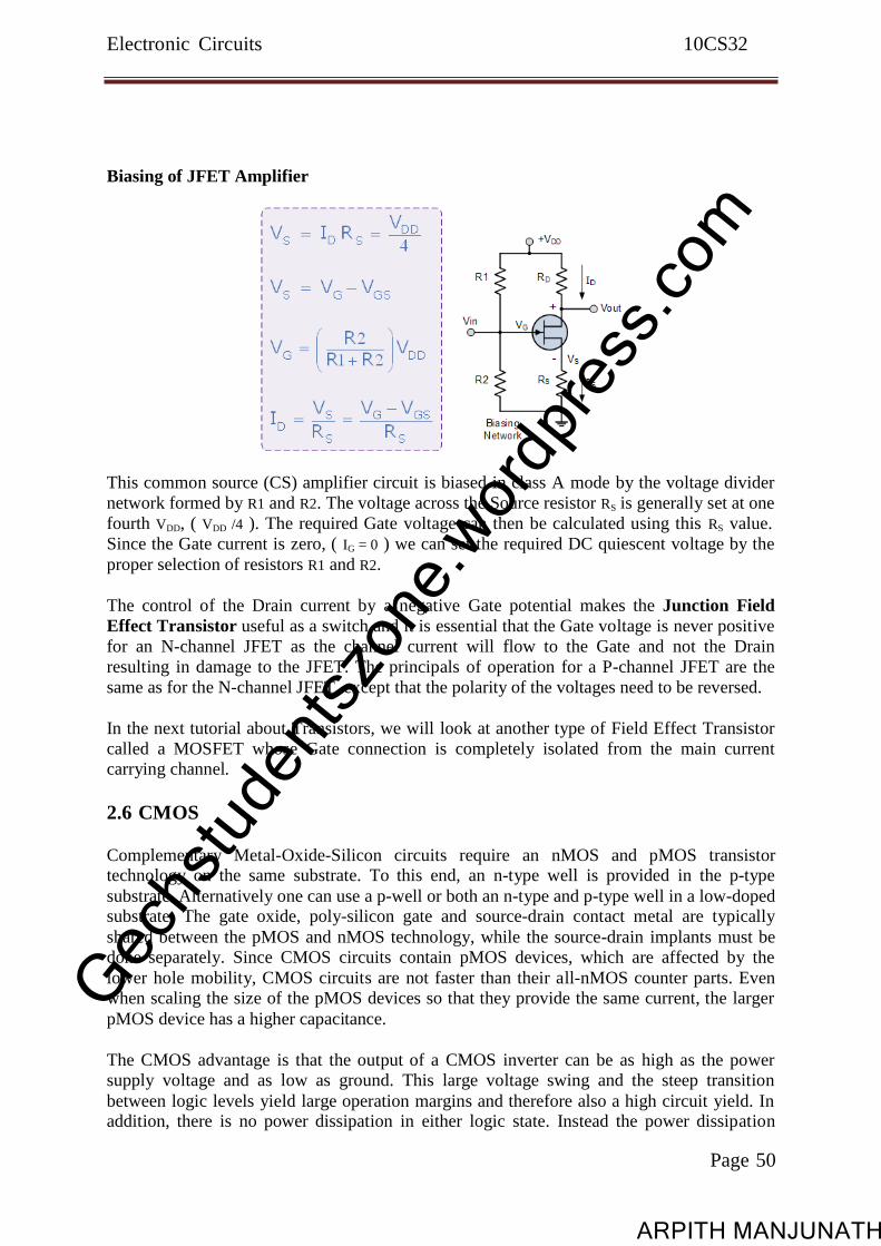
2.5 JFET Amplifier
Just like the bipolar junction transistor, JFET's can be used to make single stage class A amplifier circuits with the JFET common source amplifier and characteristics being very
similar to the BJT common emitter circuit. The main advantage JFET amplifiers have over
BJT amplifiers is their high input impedance which is controlled by the Gate biasing resistive
network formed by R1 and R2 as shown.
Page 49
Gec
hstu
dent
szon
e.w
ordp
ress
.com
ARPITH MANJUNATH
Electronic Circuits 10CS32
Biasing of JFET Amplifier
This common source (CS) amplifier circuit is biased in class A mode by the voltage divider
network formed by R1 and R2. The voltage across the Source resistor RS is generally set at one
fourth VDD, ( VDD /4 ). The required Gate voltage can then be calculated using this RS value.
Since the Gate current is zero, ( IG = 0 ) we can set the required DC quiescent voltage by the
proper selection of resistors R1 and R2.
The control of the Drain current by a negative Gate potential makes the Junction Field
Effect Transistor useful as a switch and it is essential that the Gate voltage is never positive
for an N-channel JFET as the channel current will flow to the Gate and not the Drain
resulting in damage to the JFET. The principals of operation for a P-channel JFET are the
same as for the N-channel JFET, except that the polarity of the voltages need to be reversed.
In the next tutorial about Transistors, we will look at another type of Field Effect Transistor
called a MOSFET whose Gate connection is completely isolated from the main current
carrying channel.
2.6 CMOS
Complementary Metal-Oxide-Silicon circuits require an nMOS and pMOS transistor technology on the same substrate. To this end, an n-type well is provided in the p-type
substrate. Alternatively one can use a p-well or both an n-type and p-type well in a low-doped substrate. The gate oxide, poly-silicon gate and source-drain contact metal are typically
shared between the pMOS and nMOS technology, while the source-drain implants must be
done separately. Since CMOS circuits contain pMOS devices, which are affected by the
lower hole mobility, CMOS circuits are not faster than their all-nMOS counter parts. Even
when scaling the size of the pMOS devices so that they provide the same current, the larger
pMOS device has a higher capacitance.
The CMOS advantage is that the output of a CMOS inverter can be as high as the power
supply voltage and as low as ground. This large voltage swing and the steep transition
between logic levels yield large operation margins and therefore also a high circuit yield. In addition, there is no power dissipation in either logic state. Instead the power dissipation
Page 50
Gec
hstu
dent
szon
e.w
ordp
ress
.com
ARPITH MANJUNATH

Electronic Circuits 10CS32
occurs only when a transition is made between logic states. CMOS circuits are therefore not
faster than nMOS circuits but are more suited for very/ultra large-scale integration
(VLSI/ULSI).
CMOS circuits have one property, which is very undesirable, namely latchup. Latchup occurs when four alternating p-type and n-type regions are brought in close proximity. Together they
form two bipolar transistors, one npn and one pnp transistor. The base of each transistor is connected to the collector of the other, forming a cross-coupled thyristor-like combination.
As a current is applied to the base of one transistor, the current is amplified by the transistor
and provided as the base current of the other one. If the product of the current gain of both
transistors is larger than unity, the current through both devices increases until the series
resistances of the circuit limits the current. Latchup therefore results in excessive power
dissipation and faulty logic levels in the gates affected. In principle, this effect can be
eliminated by separating the n-type and p-type device. A more effective and less space-
consuming solution is the use of trenches, which block the minority carrier flow. A deep and
narrow trench is etched between all n-type and p-type wells, passivated and refilled with an
insulating layer.
VMOS Transistors and UMOS
The VMOS transistor, named after the V-shaped groove, is a vertical MOSFET with high
current handling capability as well as high blocking voltage. It consists of a double diffused
n+/p layer, which is cut by a V-shaped groove. The V-groove is easily fabricated by
anisotropically etching a (100) silicon surface using a concentrated KOH solution. The V-
groove is then coated with a gate oxide, followed by the gate electrode. As the V-groove cuts
through the double diffused layer, it creates two vertical MOSFETs, one on each side of the
groove. The combination of the V-groove with the double diffused layers results in a short
gate length, which is determined by the thickness of the p-type layer. The vertical structure
allows the use of a low-doped drain region, which results in a high blocking voltage.
Figure: Insulated Gate Bipolar Transistor (IGBT): a) equivalent circuit and b) device cross-
section.
Page 51
Gec
hstu
dent
szon
e.w
ordp
ress
.com
ARPITH MANJUNATH

Electronic Circuits 10CS32
2.7 Recommended Questions
1. Draw and explain the base biased amplifier.
2. Draw a typical common emitter amplifier and explain the function of each component
in it.
3. Explain the single stage CE amplifier.
4. Draw the dc and ac equivalent circuits for base bias, voltage divider and two supply
emitter bias transistor circuits.
5. For the VBD amplifier shown below, draw the DC equivalent circuit and find the
6. DC quantities IE, VE, VCE and VC. (Jul-2009)
7. Explain with a neat circuit diagram and a.c equivalent circuit, the working of base
biased amplifier. (Jan-2010)
8. Sketch the output waveform for the clipper circuit of Fig.Q2 (b) shown below.
9. Assume silicon diode and obtain the peak magnitude of the output waveform.
(Jan-2010)
10. Find the voltage gain and output voltage across the load resistor for the given circuit
of FigQ2( C ) (Jan-2010)
11. Explain with a neat circuit diagram, voltage divider bias amplifier by mentioning the
importance of bypass capacitor. (Jun-2010)
, Page 52
Gec
hstu
dent
szon
e.w
ordp
ress
.com
ARPITH MANJUNATH