16 channels led driver with error detection current gain control …€¦ · · 2014-11-27•...
TRANSCRIPT

This is preliminary information on a new product now in development or undergoing evaluation. Details are subject to change without notice.
August 2013 DocID024395 Rev 3 1/41
41
LED1642GW
16 channels LED driver with error detection current gain control and12/16-bit PWM brightness control
Datasheet - preliminary data
Features• 16 constant current output channels
• Output current: from 3 mA to 40 mA
• Current programmable through external resistor
• 7-bit global current gain adjustment in two ranges
• 12/16-bit PWM grayscale brightness control
• Programmable output turn-on/off time
• Error detection mode (both open and shorted-LED)
• Programmable shorted-LED detection thresholds
• Auto power saving/auto-wakeup
• Selectable SDO synchronization on the CLK falling edge
• Gradual output delay (selectable)
• Supply voltage: 3 V to 5.5 V
• Thermal shutdown and overtemperature alert
• 30 MHz 4-wires interface
• 20 V current generator rated voltage
Applications• Full color/monochrome large displays
• LED signage
DescriptionThe LED1642GW is a monolithic, low voltage, low current power 16-bit shift register designed for LED panel displays. The LED1642GW guarantees 20 V output driving capability allowing the user to connect several LEDs in series. In the output stage, sixteen regulated current sources provide from 3 mA to 40 mA constant current to drive the LEDs. The current is programmed through an external resistor and can be adjusted by 7-bit current gain register in two subranges.The brightness can be adjusted separately for each channel through a 12/16-bit grayscale control.
A programmable turn-on and turn-off time (four different values are available) improves the system low noise generation performances.
In the LED1642GW is available the open/short error detection mode. The auto power shutdown and auto power-on feature (this feature is selectable) allow the device to save power without any external intervention.
Thermal management is equipped with overtemperature data alert and the output thermal shutdown (170 °C). The high clock frequency is up to 30 MHz and it makes the device suitable for high data rate transmission. A selectable gradual output delay reduces the inrush current whereas the selectable SDO synchronization feature works when the device is used in daisy chain configuration. The supply voltage range is between 3 V and 5.5 V.
TSSOP24 TSSOP24(exposed pad)
QSOP-24
www.st.com

Contents LED1642GW
2/41 DocID024395 Rev 3
Contents
1 Pin description . . . . . . . . . . . . . . . . . . . . . . . . . . . . . . . . . . . . . . . . . . . . . 6
2 Absolute maximum ratings . . . . . . . . . . . . . . . . . . . . . . . . . . . . . . . . . . . 7
3 Thermal characteristics . . . . . . . . . . . . . . . . . . . . . . . . . . . . . . . . . . . . . . 8
4 Electrical characteristics . . . . . . . . . . . . . . . . . . . . . . . . . . . . . . . . . . . . . 8
5 Switching characteristics . . . . . . . . . . . . . . . . . . . . . . . . . . . . . . . . . . . . 12
6 Simplified internal block diagram . . . . . . . . . . . . . . . . . . . . . . . . . . . . . 14
6.1 Equivalent circuits of inputs and outputs . . . . . . . . . . . . . . . . . . . . . . . . . 14
7 Digital blocks . . . . . . . . . . . . . . . . . . . . . . . . . . . . . . . . . . . . . . . . . . . . . . 15
8 Configuration register . . . . . . . . . . . . . . . . . . . . . . . . . . . . . . . . . . . . . . . 17
8.1 Gain control (from CFG 0 to 5) and current ranges (CFG- 6) . . . . . . . . . 18
8.2 Error detection mode (CFG-7) . . . . . . . . . . . . . . . . . . . . . . . . . . . . . . . . . 20
8.3 Error detection conditions . . . . . . . . . . . . . . . . . . . . . . . . . . . . . . . . . . . . . 23
8.4 Auto-wakeup/auto power shutdown (CFG-10) . . . . . . . . . . . . . . . . . . . . . 23
8.5 Programmable turn-on/turn-off time (CFG-11/12) . . . . . . . . . . . . . . . . . . 23
8.6 SDO delay (CFG-13) . . . . . . . . . . . . . . . . . . . . . . . . . . . . . . . . . . . . . . . . 24
8.7 Gradual output delay (CFG-14) . . . . . . . . . . . . . . . . . . . . . . . . . . . . . . . . 25
8.8 PWM counter setting and brightness register (CFG-15) . . . . . . . . . . . . . 26
9 Thermal flag . . . . . . . . . . . . . . . . . . . . . . . . . . . . . . . . . . . . . . . . . . . . . . . 28
10 Dropout voltage . . . . . . . . . . . . . . . . . . . . . . . . . . . . . . . . . . . . . . . . . . . . 29
11 Package mechanical data . . . . . . . . . . . . . . . . . . . . . . . . . . . . . . . . . . . . 30
12 Packaging mechanical data . . . . . . . . . . . . . . . . . . . . . . . . . . . . . . . . . . 37

DocID024395 Rev 3 3/41
LED1642GW Contents
13 Ordering information . . . . . . . . . . . . . . . . . . . . . . . . . . . . . . . . . . . . . . . . 39
14 Revision history . . . . . . . . . . . . . . . . . . . . . . . . . . . . . . . . . . . . . . . . . . . . 40

List of tables LED1642GW
4/41 DocID024395 Rev 3
List of tables
Table 1. Pin description . . . . . . . . . . . . . . . . . . . . . . . . . . . . . . . . . . . . . . . . . . . . . . . . . . . . . . . . . . . 6Table 2. Absolute maximum ratings . . . . . . . . . . . . . . . . . . . . . . . . . . . . . . . . . . . . . . . . . . . . . . . . . . 7Table 3. Thermal characteristics. . . . . . . . . . . . . . . . . . . . . . . . . . . . . . . . . . . . . . . . . . . . . . . . . . . . . 8Table 4. Electrical characteristics . . . . . . . . . . . . . . . . . . . . . . . . . . . . . . . . . . . . . . . . . . . . . . . . . . . . 8Table 5. Switching characteristics . . . . . . . . . . . . . . . . . . . . . . . . . . . . . . . . . . . . . . . . . . . . . . . . . . 12Table 6. Programmable TON/TOFF (output rise and fall time). . . . . . . . . . . . . . . . . . . . . . . . . . . . . 13Table 7. Digital key summary . . . . . . . . . . . . . . . . . . . . . . . . . . . . . . . . . . . . . . . . . . . . . . . . . . . . . . 15Table 8. Configuration register . . . . . . . . . . . . . . . . . . . . . . . . . . . . . . . . . . . . . . . . . . . . . . . . . . . . . 17Table 9. Example of current ranges . . . . . . . . . . . . . . . . . . . . . . . . . . . . . . . . . . . . . . . . . . . . . . . . . 19Table 10. Gain steps for the current range selected by REXT = 11 kW . . . . . . . . . . . . . . . . . . . . . . . 19Table 11. Diagnostic thresholds . . . . . . . . . . . . . . . . . . . . . . . . . . . . . . . . . . . . . . . . . . . . . . . . . . . . . 23Table 12. Minimum dropout voltage for some current values. . . . . . . . . . . . . . . . . . . . . . . . . . . . . . . 29Table 13. QSOP-24 mechanical data . . . . . . . . . . . . . . . . . . . . . . . . . . . . . . . . . . . . . . . . . . . . . . . . . 30Table 14. QFN-24 mechanical data . . . . . . . . . . . . . . . . . . . . . . . . . . . . . . . . . . . . . . . . . . . . . . . . . . 32Table 15. TSSOP24 mechanical data . . . . . . . . . . . . . . . . . . . . . . . . . . . . . . . . . . . . . . . . . . . . . . . . 34Table 16. TSSOP24 exposed pad mechanical data. . . . . . . . . . . . . . . . . . . . . . . . . . . . . . . . . . . . . . 35Table 17. TSSOP24 and TSSOP24 exposed pad tape and reel mechanical data. . . . . . . . . . . . . . . 37Table 18. Ordering information . . . . . . . . . . . . . . . . . . . . . . . . . . . . . . . . . . . . . . . . . . . . . . . . . . . . . . 39Table 19. Document revision history . . . . . . . . . . . . . . . . . . . . . . . . . . . . . . . . . . . . . . . . . . . . . . . . . 40

DocID024395 Rev 3 5/41
LED1642GW List of figures
List of figures
Figure 1. TSSOP24, TSSOP24EP, QSOP-24 pinout . . . . . . . . . . . . . . . . . . . . . . . . . . . . . . . . . . . . . 6Figure 2. QFN-24 pinout . . . . . . . . . . . . . . . . . . . . . . . . . . . . . . . . . . . . . . . . . . . . . . . . . . . . . . . . . . . 6Figure 3. Typical chip-to-chip accuracy . . . . . . . . . . . . . . . . . . . . . . . . . . . . . . . . . . . . . . . . . . . . . . . 11Figure 4. Typical application schematic . . . . . . . . . . . . . . . . . . . . . . . . . . . . . . . . . . . . . . . . . . . . . . . 11Figure 5. Timing for clock, serial in, serial out, latch enable and outputs. . . . . . . . . . . . . . . . . . . . . . 13Figure 6. LED1642GW simplified block diagram . . . . . . . . . . . . . . . . . . . . . . . . . . . . . . . . . . . . . . . . 14Figure 7. Input and output equivalent circuits . . . . . . . . . . . . . . . . . . . . . . . . . . . . . . . . . . . . . . . . . . 14Figure 8. Digital keys . . . . . . . . . . . . . . . . . . . . . . . . . . . . . . . . . . . . . . . . . . . . . . . . . . . . . . . . . . . . . 16Figure 9. Channel data and write switch . . . . . . . . . . . . . . . . . . . . . . . . . . . . . . . . . . . . . . . . . . . . . . 16Figure 10. Channel current vs. gain register value . . . . . . . . . . . . . . . . . . . . . . . . . . . . . . . . . . . . . . . 20Figure 11. Error detection action sequence . . . . . . . . . . . . . . . . . . . . . . . . . . . . . . . . . . . . . . . . . . . . . 21Figure 12. Error detection power-on timing . . . . . . . . . . . . . . . . . . . . . . . . . . . . . . . . . . . . . . . . . . . . . 21Figure 13. Configuration register reading sequence . . . . . . . . . . . . . . . . . . . . . . . . . . . . . . . . . . . . . . 22Figure 14. Configuration register reading sequence (zoom) . . . . . . . . . . . . . . . . . . . . . . . . . . . . . . . . 22Figure 15. Configuration register reading sequence - SDO delay actives . . . . . . . . . . . . . . . . . . . . . . 22Figure 16. Configuration register reading sequence - SDO delay actives (zoom). . . . . . . . . . . . . . . . 22Figure 17. Output TON (current rise time) CFG - 12 = CFG - 11 = 0. . . . . . . . . . . . . . . . . . . . . . . . . . 24Figure 18. Output TOFF (current fall time) CFG -12 = CFG - 11 = 0. . . . . . . . . . . . . . . . . . . . . . . . . . 24Figure 19. Output TON (current rise time) CFG -12 = CFG - 11 = 1 . . . . . . . . . . . . . . . . . . . . . . . . . . 24Figure 20. Output TOFF (current fall time) CFG -12 = CFG - 11 = 1. . . . . . . . . . . . . . . . . . . . . . . . . . 24Figure 21. SDO delay . . . . . . . . . . . . . . . . . . . . . . . . . . . . . . . . . . . . . . . . . . . . . . . . . . . . . . . . . . . . . 25Figure 22. PWCLK counter and comparator . . . . . . . . . . . . . . . . . . . . . . . . . . . . . . . . . . . . . . . . . . . . 27Figure 23. Brightness register setting . . . . . . . . . . . . . . . . . . . . . . . . . . . . . . . . . . . . . . . . . . . . . . . . . 27Figure 24. Thermal flag status . . . . . . . . . . . . . . . . . . . . . . . . . . . . . . . . . . . . . . . . . . . . . . . . . . . . . . . 28Figure 25. Typical channel dropout voltage vs. output current (VDD = 3.3 V). . . . . . . . . . . . . . . . . . . 29Figure 26. QSOP-24 package dimensions . . . . . . . . . . . . . . . . . . . . . . . . . . . . . . . . . . . . . . . . . . . . . 31Figure 27. QFN-24 package dimensions . . . . . . . . . . . . . . . . . . . . . . . . . . . . . . . . . . . . . . . . . . . . . . . 33Figure 28. TSSOP24 package dimensions . . . . . . . . . . . . . . . . . . . . . . . . . . . . . . . . . . . . . . . . . . . . . 34Figure 29. TSSOP24 exposed pad dimensions. . . . . . . . . . . . . . . . . . . . . . . . . . . . . . . . . . . . . . . . . . 36Figure 30. TSSOP24 and TSSOP24 exposed pad tape and reel dimensions. . . . . . . . . . . . . . . . . . . 38
Pin description LED1642GW
6/41 DocID024395 Rev 3
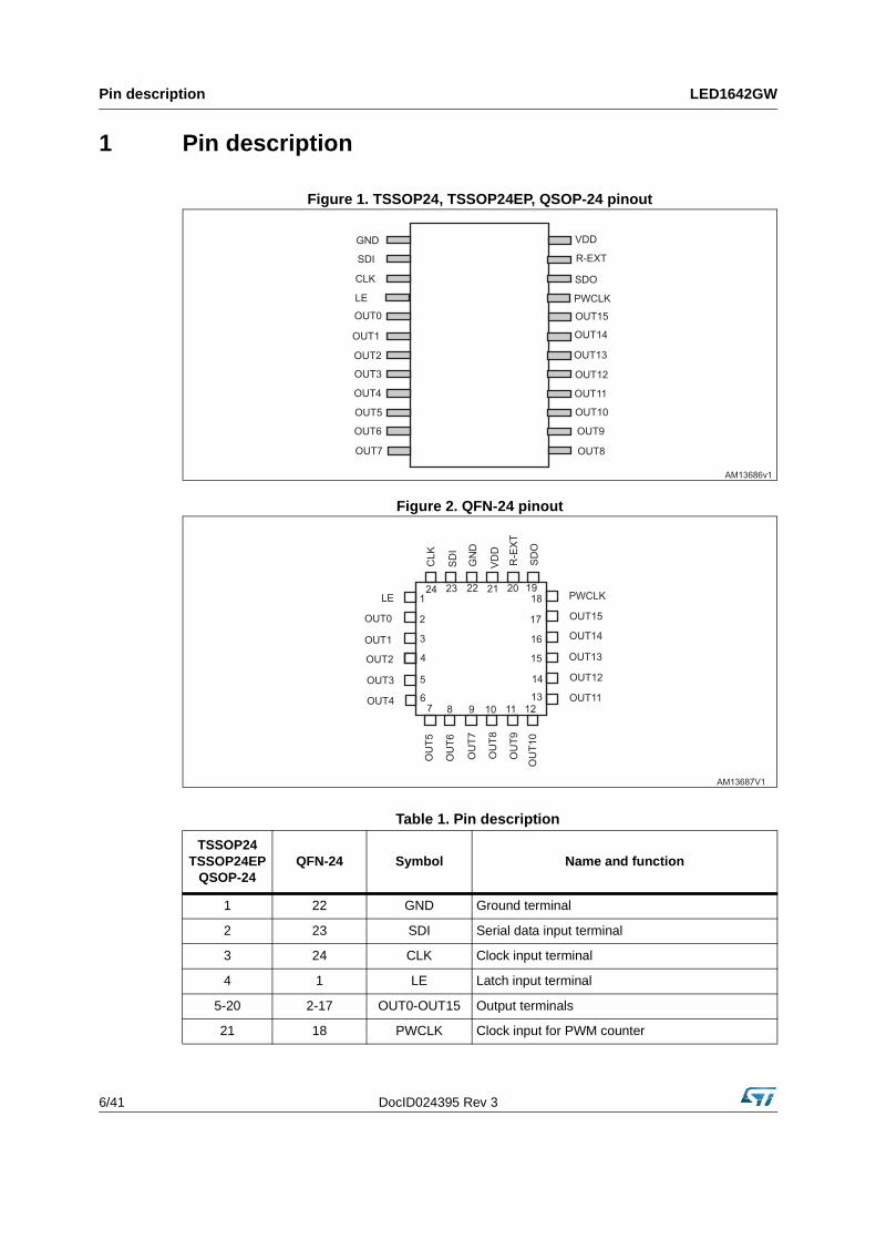
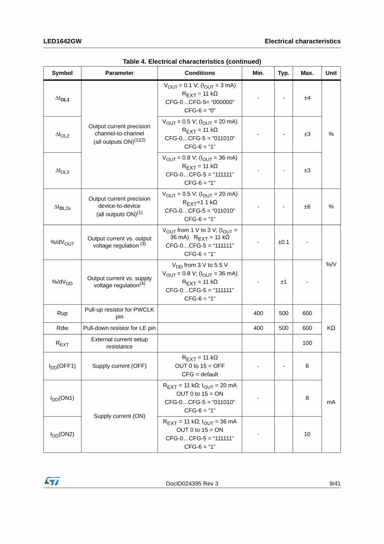
1 Pin description
Figure 1. TSSOP24, TSSOP24EP, QSOP-24 pinout
Figure 2. QFN-24 pinout
Table 1. Pin description
TSSOP24 TSSOP24EP
QSOP-24QFN-24 Symbol Name and function
1 22 GND Ground terminal
2 23 SDI Serial data input terminal
3 24 CLK Clock input terminal
4 1 LE Latch input terminal
5-20 2-17 OUT0-OUT15 Output terminals
21 18 PWCLK Clock input for PWM counter
GND
SDI
CLK
LE
OUT0
OUT1
OUT2
OUT3
OUT4
OUT5
OUT6
OUT7 OUT8
OUT9
OUT10
OUT11
OUT12
OUT13
OUT14
OUT15
PWCLK
SDO
R-EXT
VDD
AM13686v1
AM13687V1
1
2
3
4
5
67 8 9 10 11 12
13
14
15
16
17
18192021222324
LE
OUT0
OUT1
OUT2
OUT3
OUT4
OU
T5
OU
T6
OU
T7
OU
T8
OU
T9
OU
T10
OUT11
OUT12
OUT13
OUT14
OUT15
PWCLK
CLK
SD
I
GN
D
VD
D
R-E
XT
SD
O

DocID024395 Rev 3 7/41
LED1642GW Absolute maximum ratings
2 Absolute maximum ratings
Stressing the device above the ratings listed in the Table 2 may cause the device permanent damage. Operating under conditions above those indicated in the operating section is not implied. Exposure to absolute maximum rating conditions for extended periods may affect the device reliability.
22 19 SDO Serial data output terminal
23 20 R-EXTTerminal for external resistor for constant current programming
24 21 VDD Supply voltage terminal
Table 1. Pin description (continued)
TSSOP24 TSSOP24EP
QSOP-24QFN-24 Symbol Name and function
Table 2. Absolute maximum ratings
Symbol Parameter Value Unit
VDD Supply voltage 0 to 7 V
VOUT Output voltage -0.5 to 20 V
IOUT Output current 50 mA
Vi Input voltage -0.4 to VDD +0.4 V
IGND GND terminal current 1400 mA
ESDElectrostatic discharge protection
HBM human body model±2 kV

Thermal characteristics LED1642GW
8/41 DocID024395 Rev 3
3 Thermal characteristics
4 Electrical characteristics
VDD = 3.3 V, Tj = 25 °C, unless otherwise specified.
Table 3. Thermal characteristics
Symbol Parameter Value Unit
Ta Operative free-air temperature range(1) -40 to +85
°CTOPR Operative junction temperature range -40 to +125
TSTG Storage ambient temperature range -55 to +150
Rthj-amb Thermal resistance junction-ambient
QFN-24 30
°C/WTSSOP24 85
TSSOP24EP(2) 37.5
QSOP-24 72
1. This data must be considered in adequate power dissipation conditions, the junction temperature must be maintained below 125 °C.
2. The exposed pad should be soldered directly to the PCB to get the thermal benefits.
Table 4. Electrical characteristics
Symbol Parameter Conditions Min. Typ. Max. Unit
VDD Supply voltage 3 5.5
V
VOUT Output voltage Out 0 - out 15 - - 19
VIHInput voltage
0.7 x VDD - VDD
VIL GND - 0.3 x VDD
VOL Serial data output voltage (SDO)
VDD= 3 to 5.5 VI = +/- 1 mA
- - 0.4
VOH VDD -0.4 - -
IOleak Output leakage current VOUT = 19 V, all outputs OFF - - 0.5 µA
Vuvlo
UVLO threshold (rising) 2.7 2.9V
UVLO threshold (falling) 2.2 2.3
Hyuvlo UVLO hysteresis 400 mV
DocID024395 Rev 3 9/41
LED1642GW Electrical characteristics
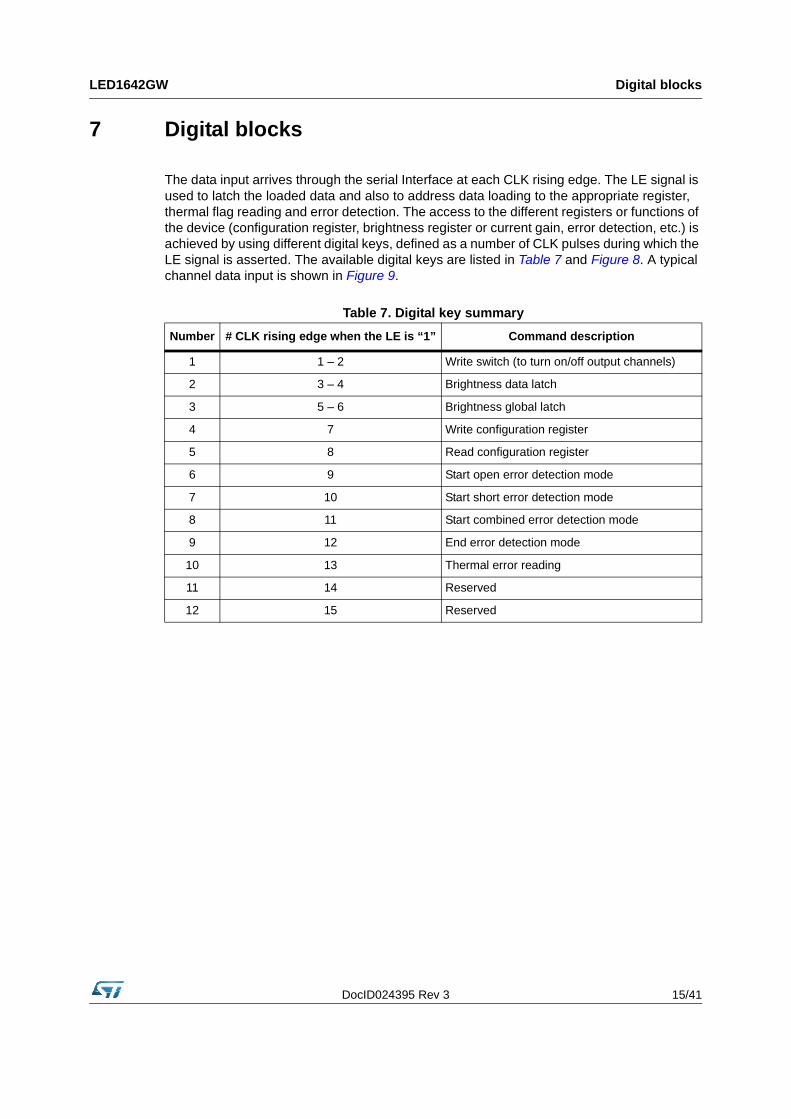
∆IOL1
Output current precision channel-to-channel(all outputs ON)(1)(2)
VOUT = 0.1 V; (IOUT = 3 mA)REXT = 11 kΩ
CFG-0…CFG-5= “000000”CFG-6 = “0”
- - ±4
%∆IOL2
VOUT = 0.5 V; (IOUT = 20 mA) REXT = 11 kΩ
CFG-0…CFG-5 = “011010”
CFG-6 = “1”
- - ±3
∆IOL3
VOUT = 0.8 V; (IOUT = 36 mA)
REXT = 11 kΩCFG-0…CFG-5 = “111111”
CFG-6 = “1”
- - ±3
∆IOL2a
Output current precision device-to-device
(all outputs ON)(1)
VOUT = 0.5 V; (IOUT = 20 mA) REXT=1 1 kΩ
CFG-0…CFG-5 = “011010”CFG-6 = “1”
- - ±6 %
%/dVOUTOutput current vs. output
voltage regulation (3)
VOUT from 1 V to 3 V; (IOUT = 36 mA) REXT = 11 kΩ
CFG-0…CFG-5 = “111111”CFG-6 = “1”
- ±0.1 -
%/V
%/dVDDOutput current vs. supply
voltage regulation(4)
VDD from 3 V to 5.5 VVOUT = 0.8 V; (IOUT = 36 mA)
REXT = 11 kΩCFG-0…CFG-5 = “111111”
CFG-6 = “1”
- ±1 -
RupPull-up resistor for PWCLK
pin400 500 600
KΩRdw Pull-down resistor for LE pin 400 500 600
REXTExternal current setup
resistance100
IDD(OFF1) Supply current (OFF)REXT = 11 kΩ
OUT 0 to 15 = OFF
CFG = default
- - 6
mAIDD(ON1)
Supply current (ON)
REXT = 11 kΩ; IOUT = 20 mA
OUT 0 to 15 = ONCFG-0…CFG-5 = “011010”
CFG-6 = “1”
- 8
IDD(ON2)
REXT = 11 kΩ; IOUT = 36 mAOUT 0 to 15 = ON
CFG-0…CFG-5 = “111111”CFG-6 = “1”
- 10
Table 4. Electrical characteristics (continued)
Symbol Parameter Conditions Min. Typ. Max. Unit
Electrical characteristics LED1642GW
10/41 DocID024395 Rev 3
IDD (auto OFF)
Supply current (auto OFF)
REXT= 11 kΩ;OUT 0 to 15 = OFF
CFG-0…CFG-5 = “111111”CFG-6 = “1”
- 200 500 µA
Tflg Thermal flag 150
°CTsd Thermal shutdown 170
Tsd-hyThermal shutdown
hysteresis15 20
1. Tested with just one output loaded.
2. ((Ioutn - Ioutavg1-15)/ Ioutavg1-15) x 100.
3.
4.
Table 4. Electrical characteristics (continued)
Symbol Parameter Conditions Min. Typ. Max. Unit
13
100)V0.1Voutn@Ioutn(
)V0.1Voutn@Ioutn()V0.3Voutn@Ioutn()V/(%
−×
==−==Δ
35.5
100)V0.3V dd@Ioutn(
)V0.3Vdd@Ioutn()V5.5V dd@Ioutn()V/(%
−×
==−==Δ

DocID024395 Rev 3 11/41
LED1642GW Electrical characteristics
Figure 3. Typical chip-to-chip accuracy
Figure 4. Typical application schematic
AM13688V1
0
0.5
1
1.5
2
2.5
3
3.5
4
0 5 10 15 20 25 30 35 40
Chi
p-to
-chi
p (%
)
IOUT (mA)
VDD=3.3/5 V; T=25 ° C
AM13689V1
LED1642GW
Supply voltageSDI
CLK
LE
PWCLK
VDD OUT0 OUT1 OUT15
R-EXT
Current setting resistor
Data loaded through serial
interface
LED common rail voltage
…..
SDO Data output
+
Cin
Cled
GND

Switching characteristics LED1642GW
12/41 DocID024395 Rev 3
5 Switching characteristics
VDD = 3.3 V, Tj = 25 °C, unless otherwise specified.
Table 5. Switching characteristics
Symbol Parameter Conditions Min. Typ. Max. Unit
fclk Clock frequency Cascade operation - - 30MHz
fpwclk PWclock frequency - - 30
tr(SDO) SDO rise timeREXT= 11 kΩ; IOUT = 20 mA
VOUT = 0.8 VVIH = VDD; VIL = GND
RL = 3.3 KΩ; CL = 10 pF
CFG-0…CFG-5 = “011010”CFG-6 = “1”
- 5 -
ns
tf(SDO) SDO fall time - 5 -
tPLHLE LE - OUTn(1)Propagation delay
time
(“L to “H”)
REXT = 11 kΩ; IOUT = 20 mAVOUT = 0.8 V
VIH = VDD; VIL = GNDRL = 50 Ω; CL = 10 pF
CFG-0…CFG-5 = “011010”
CFG-6 = “1”
- 200 -
tPLHCLK - SDO
CFG-13 = ‘0’8 15 25
tPHLLE LE - OUTn(1)Propagation delay
time(“H” to “L”)
- 100 -
tPHLCLK - SDO
CFG-13 = ‘0’8 15 25
tw(CLK) CLK
Pulse width
20 - -
tW(PWCLK) PWCLK 20 - -
tw(L) LE 20 - -
tgr-d Gradual delay ch-to-ch 10
tsu(L) Setup time for LE 5 - -
th(L) Hold time for LE 5 - -
tsu(D) Setup time for SDI 5 - -
th(D) Hold time for SDI 10 - -
tclkr(2) Maximum CLK rise time - - 5µs
tclkf(2) Maximum CLK fall time - - 5
Iout-ov Output current turn-on overshootVOUT = 0.6 to 3 V
CL = 10 pF; IOUT = 3 to 36 mA- - 10 %
tn-errNormal error detection
minimum output ON time- - 1 µs
tshutdown Auto power shutdown time (auto OFF)From LE falling edge to REXT
voltage reference at -10%- 100 - ns
twakeup Auto-wakeup From LE falling edge to REXT
voltage reference at 90%- 3 - µs
1. CFG -11= 0 and CFG -12 = 0 (output tr = 30 ns; output tf = 20 ns); CFG-14=1 (no output gradual delay).
2. If devices are connected in cascade and tclkr or tclkf is large, it may be critical to achieve the timing required for data transfer between two cascaded devices.

DocID024395 Rev 3 13/41
LED1642GW Switching characteristics
Figure 5. Timing for clock, serial in, serial out, latch enable and outputs
The correct sampling of the data depends on the stability of the data at SDI on the rising edge of the clock signal and it is assured by a proper data setup and hold time (tSU(D) and th(D)), as shown in Figure 5. The same figure shows the propagation delay from CLK to SDO (tPLH/tPHL). Figure 5 describes also the minimum duration of CLK, LE pulses (tW(CLK)) and tW(L) respectively and the propagation delay from LE to OUTn (tPLHLE and tPHLLE) in the hypothesis that all channels have already been enabled by PWM counter.
Table 6. Programmable TON/TOFF (output rise and fall time)
Configuration bits
(CFG-12 - CFG-11)Conditions
Typ. (20% to 80%)Unit
Turn-on Turn-off
0 - 0 REXT = 11 kΩ; IOUT = 20 mAVOUT = 0.8 V
VIH= VDD; VIL= GND
RL = 50 Ω; CL=10pFCFG-0...CFG-5=“011010”
CFG-6 = “1”
30 ns 20 ns
ns
0 - 1 100 ns 40 ns
1 - 0 140 ns 80 ns
1 - 1 180 ns 150 ns
tpLHLE, tpHLLE
AM13690V1

Simplified internal block diagram LED1642GW
14/41 DocID024395 Rev 3
6 Simplified internal block diagram
Figure 6. LED1642GW simplified block diagram
6.1 Equivalent circuits of inputs and outputsLE and PWCLK input terminals have pull-down and pull-up connection respectively. CLK and SDI must be connected to the external circuit to fix the logic level.
Figure 7. Input and output equivalent circuits
AM13691V1
UVLO & POR
Configuration register
Channel driverTiming controlTurn ON/OFFGradual delay
……
……
Current gain adjustment
SDICLKLE
VDD
GND
R-EXT
SDO
OUT0
OUT1
OUT2
OUT14
OUT15
16 output channels
PWM counter
PWCLK
Thermal shutdown
CurrentRef.
Control Logic &Data Registers
Error detection
AM13692V1
PWCLK terminal LE terminal
CLK, SDI terminal SDO terminal
DocID024395 Rev 3 15/41
LED1642GW Digital blocks
7 Digital blocks
The data input arrives through the serial Interface at each CLK rising edge. The LE signal is used to latch the loaded data and also to address data loading to the appropriate register, thermal flag reading and error detection. The access to the different registers or functions of the device (configuration register, brightness register or current gain, error detection, etc.) is achieved by using different digital keys, defined as a number of CLK pulses during which the LE signal is asserted. The available digital keys are listed in Table 7 and Figure 8. A typical channel data input is shown in Figure 9.
Table 7. Digital key summary
Number # CLK rising edge when the LE is “1” Command description
1 1 – 2 Write switch (to turn on/off output channels)
2 3 – 4 Brightness data latch
3 5 – 6 Brightness global latch
4 7 Write configuration register
5 8 Read configuration register
6 9 Start open error detection mode
7 10 Start short error detection mode
8 11 Start combined error detection mode
9 12 End error detection mode
10 13 Thermal error reading
11 14 Reserved
12 15 Reserved

Digital blocks LED1642GW
16/41 DocID024395 Rev 3
Figure 8. Digital keys
Figure 9. Channel data and write switch
AM13693V1
CLK
LE
LE
LE
LE
LE
LE
LE
LE
LE
Write switch
Data latch
Global latch
Write CR
Read CR
Start open error detection
Start short error detection
Start combined detection
End error detection
LE Thermal error reading
AM13694V1
0E0F 0C 0A0B0D 09 08 07 06 05 04 03 02 01 00
CLK
SDI
LE
16-bit data

DocID024395 Rev 3 17/41
LED1642GW Configuration register
8 Configuration register
The configuration register is used to enable or disable some device features, to program some parameters and to change other settings. The access to this register (read or write) is managed to find a description for each bit as described in Table 8. The default value of the configuration register (when the device is switched on or after a reset) is "0" for all bits. To change anything in the configuration register, a 16-bit digital word must be sent (CFG - 0 represents LSB, CFG -15 the MSB).
Table 8. Configuration register
Bit Definition R/W Description Default
CFG-0
Current gain adjustment
R/W6-bit DAC allows adjusting the device output current in 64 steps for each range (defined by CFG-6)
0
CFG-1 0
CFG-2 0
CFG-3 0
CFG-4 0
CFG-5 0
CFG-6 Current range R/W”0” low current range
“1” high current range0
CFG-7Error detection
modeR/W
“0” normal mode
“1” reserved mode0
CFG-8Shorted-LED
detection thresholds
R/W Programmable outputshorted-LED detection thresholds
CFG-9 CFG-8 Th. volt.
00 0 1.8 V
0 1 2.5 V
CFG-9 R/W1 0 3 V
01 1 3.5 V
CFG-10Auto OFF shutdown
R/W“0” device always ON”1” auto power shutdown active (auto OFF)
0
CFG-11Output turn-on/off time
R/WProgrammable output rise and fall time (20% to 80%)
CFG-12 CFG-11 Turn-on Turn-off
00 0 30 ns 20 ns
0 1 100 ns 40 ns
CFG-12 R/W1 0 140 ns 80 ns
01 1 180 ns 150 ns
CFG-13 SDO delay R/WIf “0” no delay is present on SDOIf “1” the data are shifted out and they are synchronized with the falling edge of the CLK signal
0
Configuration register LED1642GW
18/41 DocID024395 Rev 3
8.1 Gain control (from CFG 0 to 5) and current ranges (CFG- 6)The LED current can be programmed using an external resistor connected to GND from REXT pin and can be fixed using the dedicated bits of the configuration register (from CFG - 0 to CFG - 5 bits define the gain, while CFG - 6 bit defines the current range within the which the gain can be adjusted). The device can regulate the current up to 36 mA and down to 0.5 mA. The accuracy of the LED current depends on the selected range and it is guaranteed in the ranges indicated in the static electrical characteristics only (see Table 3 and 9). When the device is switched on, the selected current range and the resistor connected to the REXT pin fix the default LED current:
Where VREF=1.23 V is the voltage of the REXT pin and K is the mirroring current ratio, whose value depends on the selected current range:
• K = 28 with low current range selected (CFG - 6 = "0")
• K = 80 with high current range selected (CFG - 6 = "1")
The relation between the programmed current and the current gain settings is the following:
where G is the current gain value (decimal value) defined by the dedicated bits of the current gain register. The current gain is managed by 6-bits of the configuration register (CFG - 0 to CFG - 5, CFG - 0 is LSB and CFG - 5 is MSB) and can be adjusted within two ranges (selectable through the bit CFG - 6) over 64 steps. The width of each step depends on the default current (Iol_default) as well as the selected REXT. Finally, each step is as follows:
CFG-14Gradual output
delayR/W
“0” a progressive delay is applied to output (10 ns per channel)”1” no delay is applied to output
0
CFG-1512/16 PWM
counterR/W
“0” to select 16-bit brightness register (65536 grayscale rightness steps).
“1” to select 12-bit brightness register (4096 grayscale brightness steps)
0
Table 8. Configuration register (continued)
Bit Definition R/W Description Default
KR
VI
EXT
REFdefaultOL ⋅=_
)( _ stepdefaultOLOL IGII Δ⋅+=
DocID024395 Rev 3 19/41
LED1642GW Configuration register
The Table 9 shows an example of the current setting with an external resistance (REXT) = 11 KΩ:
The Table 10 shows an example of current setting and gain control with REXT = 11 kΩ, see also Figure 10.
The external programming resistance must be connected as close as possible to the related device pins (REXT and GND) to reduce as minimum as possible the routing length and prevent reference noise injection and electromagnetic interferences. Moreover, a direct connection to the device GND pin reduces the possible output current variation when the total device ground current changes (load effect).
Table 9. Example of current ranges
REXT [KΩ] CFG-6 CFG-0 to CFG-5 LED current(1) [mA]
1. The indicated values may be slightly different on the current device.
Accuracy
Low range11 0 000000 3.1 mA ± 4% ch-to-ch
11 0 111111 12.5 mA-
High range11 1 000000 8.9 mA
11 1 011010 20 mA ± 3% ch-to-ch
Table 10. Gain steps for the current range selected by REXT = 11 kΩ
CFG-6 CFG(0 to 5) LED current (1) [mA]
1. The indicated values may be slightly different on the current device.
Low range
0 000000 3.131
0 000001 3.280
… … …
0 111111 12.524
High range
1 000000 8.945
1 000001 9.371
… … …
1 111111 35.78
21_ d efa u ltO L
step
II =Δ

Configuration register LED1642GW
20/41 DocID024395 Rev 3
Figure 10. Channel current vs. gain register value
8.2 Error detection mode (CFG-7)Stopping the normal activity of the display and turning on all driver channels allows the error detection to be performed and failed LED or display defects to be checked.
The error detection is active when the CFG -7 bit of the configuration register is "0". The diagnostics is performed as shown in Figure 11:
• The LED has to be selected turning on the relative channel on the switch register (powering on or off the output channels); the brightness register value for this channel cannot be zero.
• The normal error detection has to be selected in the configuration register (CFG-7= "0"). The appropriate digital key to choose the type of detection (open, short or combined) must be sent (see Table 7).
• After the error detection starts, the channel under testing has to be turned on at least 1 μs (the LED is at the nominal current). Please note that, the output power-on depends on PWCLK signal and in several applications this signal is not synchronized with the serial interface clock (CLK pin). Therefore, to be sure that, between the detection start and the detection end, the output power-on is 1 μs and moreover, that last power-on, in the interval, starts at least 0.5 μs before the detection end pattern (see Figure 12), it is suggested that the error detection should be performed just after the device startup (brightness counter reset) with all channels ON, before applying PWCLK signal.
• The result of the detection ("0" indicates a fault condition) is shifted out SDO, in 16 clock pulses after the "detection end command" is provided, first output bit represents channel 15 (error data can be read in a way similar to configuration register data reading as shown on Figure 13, 14, 15 and 16).
Please note that (with SDO delay off) output 15 detection result will be available just after 1st clock pulse rising edge, so it can be sampled on the rising edge of second clock pulse. In the same way output 0 detection result will be available just after 16th clock pulse rising edge, so it can be sampled on the rising edge of 17th CLK pulse.
AM13695V1
0.0
5.0
10.0
15.0
20.0
25.0
30.0
35.0
40.0
0 5 10 15 20 25 30 35 40 45 50 55 60 65 70
11 K R=0
11 K R=118 K R=0
IOUTOUT vs. gain(R = range selection, REXT = 11 K or 18 K)
Gain register decimal value
IOU
TO
UT
(mA
) (m
A) 18 K R=1

DocID024395 Rev 3 21/41
LED1642GW Configuration register
Figure 11. Error detection action sequence
Figure 12. Error detection power-on timing
AM13696V1
Normal detection sequence
Read error detection result on SDO in 16 clock pulses after
detection end command
Turn on LED by PWCLK pulses for at least 1 µ s
Send open, short or combined error detection start command
by LE digital keys
Select LED to be turned on and checked in switch register
data; brightness for selected channels cannot be zero.
Select normal error detection modeon CFG register (bit 7 = “0”)
Send error detection end command by LE digital key
AM13697V1
0.5us Det.End
Det. Start
It must contain 1us output power ON
1us
SPI pattern
Output Current
x0000 < BRT < xFFFF

Configuration register LED1642GW
22/41 DocID024395 Rev 3
Figure 13. Configuration register reading sequence
Figure 14. Configuration register reading sequence (zoom)
CFG Reg programming CFG Reg reading command CFG Reg data
C1=CLKC2=SDIC3=LEC4=SDO
First CLK pulseafter CFG Reg
reading command
CFG Reg data
C1=CLKC2=SDIC3=LEC4=SDO
First CLK pulseafter CFG Reg
reading command
Figure 15. Configuration register reading sequence - SDO delay actives
Figure 16. Configuration register reading sequence - SDO delay actives (zoom)
CFG Reg programming CFG Reg reading command CFG Reg data
C1=CLKC2=SDIC3=LEC4=SDO
First CLK pulseafter CFG Reg
reading command
Sync. change
CFG13=1
C1=CLKC2=SDIC3=LEC4=SDO
CFG Reg data
First CLK pulseafter CFG Reg
reading command

DocID024395 Rev 3 23/41
LED1642GW Configuration register
8.3 Error detection conditionsDuring the error detection phases for each channel, the following checks have to be performed:
– The output current in open detection mode (digital key: 9 CLK rising edges when LE is "1")
– The output voltage in short detection (digital key: 10 CLK rising edges when LE is "1")
– Both parameters (output voltage and current) in combined error detection mode (digital key: 11 CLK rising edges when LE is "1").
The thresholds for the error diagnostics are listed in Table 11:
8.4 Auto-wakeup/auto power shutdown (CFG-10)This feature reduces the power consumption when all outputs are OFF. It is active when the CFG -10 bit of configuration register is "1". The auto power shutdown (auto OFF) starts when the data latched is "0" for all channels, and device is active again (wakeup) at the first latched data string including at least one bit = "1" (at least one channel ON). Timings for shutdown and wakeup are present in the dynamics feature table. While the auto power shutdown is active, the device ignores any other command except the channel power-on.
8.5 Programmable turn-on/turn-off time (CFG-11/12)The device gives the possibility to program the turn-on and turn-off time of the current generators. Four different values can be selected using CFG -12 and CFG-11 bits of the configuration register (see Table 8) to fit the application requirements: 30/20 ns (00), 100/40 ns (01), 140/80 ns (10) and 180/150 ns (11). The selected value refers to TON (current rise time) and TOFF (current fall time).
Table 11. Diagnostic thresholds
Error detection modes
Checked malfunction
CFG-9 CFG-8Thresholds (V)
Min. Typ. Max.
Open detection
Com
bine
d m
ode
Open line or output short to GND
x x -IOUT ≤ 0.5 x IOUT
programmed-
Short detection
Short on LED or short to V-LED
0 0 1.15 VOUT ≥ 1.8 2.05
0 1 2.25 VOUT ≥ 2.5 2.75
1 0 2.75 VOUT ≥ 3.0 3.25
1 1 3.25 VOUT ≥ 3.5 3.80
Configuration register LED1642GW
24/41 DocID024395 Rev 3
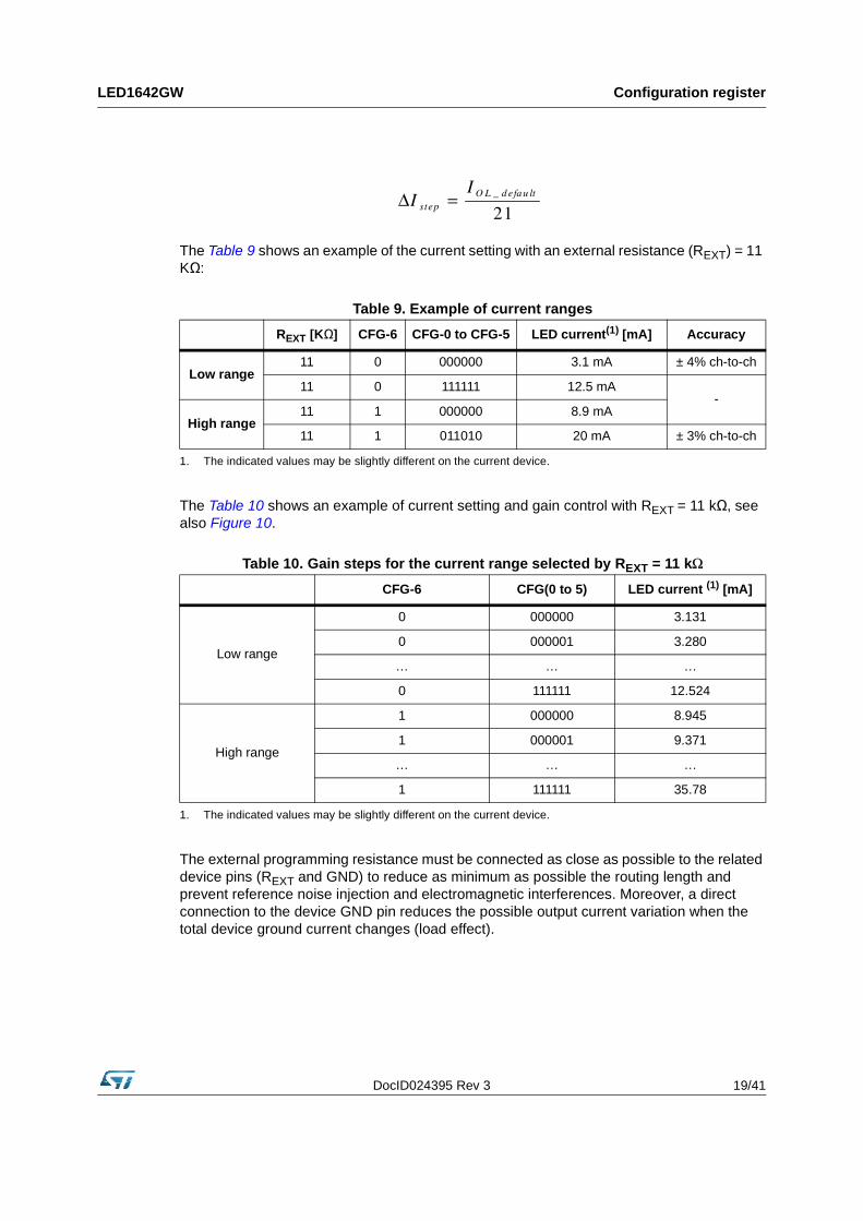
8.6 SDO delay (CFG-13)Usually in SDO terminal, data are shifted out the rising edge of CLK signal (with a propagation delay of about 15 ns - signal (a) in Figure 21). The device has the possibility to shift data out the falling edge of the CLK signal (with few ns of propagation delay - signal (b) in Figure 21). This feature is active when CFG -13 bit of the configuration register is "1". Default setting for this bit is "0" hence the SDO delay is not activated by default. This feature is particularly useful when some devices are connected in daisy chain configuration with mismatched propagation delays, between CLK and SDO data path (board routing).
Figure 17. Output TON (current rise time) CFG - 12 = CFG - 11 = 0
Figure 18. Output TOFF (current fall time) CFG -12 = CFG - 11 = 0
AM13698V1 AM13699V1
Figure 19. Output TON (current rise time) CFG -12 = CFG - 11 = 1
Figure 20. Output TOFF (current fall time) CFG -12 = CFG - 11 = 1
AM13700V1
AM13701V1

DocID024395 Rev 3 25/41
LED1642GW Configuration register
Figure 21. SDO delay
8.7 Gradual output delay (CFG-14)The gradual output delay consists of turning on gradually the current generators avoiding to turn on all channels at the same time.
When PWM counter enables the device channels, the outputs can be turned on simultaneously or with a progressive delay. Thanks to configuration register CFG -14 bit, the user can decide to put a delay among outputs (10 ns from each channel to the next one, around 150 ns between first and last channel). The typical output timing is shown in Figure . This feature prevents the inrush current and reduces the bypass capacitor value.
AM13702V1
(a)
(b)
(a) Data shifted out of the SDO with the device propagation delay(b) Data shifted out of the SDO by the falling edge of the CLK

Configuration register LED1642GW
26/41 DocID024395 Rev 3
Gradual output delay
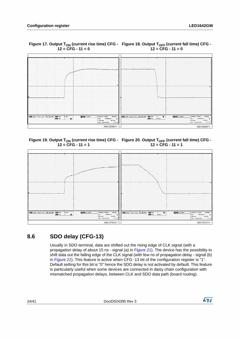
8.8 PWM counter setting and brightness register (CFG-15)The brightness of each channel can be adjusted through a 12/16-bit PWM grayscale brightness control according to the PWM counter selection (configuration register CFG -15 bit). Brightness data is loaded by the SDI pin in a 16-bit shift register. Once 16-bit has been loaded (first input bit of brightness word is MSB, 16th bit is LSB), the digital word is moved to the corresponding temporary buffer (first word is the brightness of channel 15, the last one is for channel 0) using the appropriate key shown in Table 7 ("data latch"). One "data latch" key must follow each 16-bit brightness word except the last one. When the last brightness word is loaded (channel 0 brightness data), the key indicated as "global latch" in Table 7 must be used. This action moves the word from the shift register to the temporary buffer through the OUT0 and, at the same time, transfers all data of the 16 temporary buffers (16 x16-bit string) to the corresponding brightness registers (see also Figure 27).
The PWM signals are generated by comparing the content of the brightness registers to a 16-bit or 12-bit counter, according to the CFG-15 bit status. The counter's clock source is provided to the PWCLK pin. In case of selection of 12-bit PWM counter, the four most significant bits of each brightness data word are ignored. However, each of sixteen brightness data words must be 16-bit long.The brightness register default value is "0", unless this value is changed, the LED brightness is minimum. Figure 26 shows this function in the schematic.
PWCLK must be a square wave signal, duty cycle is not important but the minimum width has to be above 20 ns, max. frequency has to be 30 MHz (pay attention the minimum output ON time). Just after the device startup (brightness counter reset), before applying PWCLK signal, all channels are in power-on condition if the brightness register values are not zeroed.
AM13703V1
DocID024395 Rev 3 27/41
LED1642GW Configuration register
Figure 22. PWCLK counter and comparator
Figure 23. Brightness register setting
AM13704V1
AM13705V1
0E0F 0C 0A0B0D 09 08 07 06 05 04 03 02 01 00
BRT14 BRT13BRT15 BRT01BRT02BRT03
256-bit brightness data stream
CLK
SDI
LE
16-bit Data Word
Data latch
CLK
SDI
LE
Global latch
0E0F 0C 0A0B0D 09 08 07 06 05 04 03 02 01 00
BRT00
MSB LSB

Thermal flag LED1642GW
28/41 DocID024395 Rev 3
9 Thermal flag
The device has a thermal control logic providing a flag status when the internal temperature exceeds 150 °C (if temperature increases over 170 °C a thermal shutdown protects the device). This status can be read running the digital key "thermal error reading", holding the LE high for 13 CLK rising edges (see Figure 24). If thermal alert is asserted, a 16-bit string = "1" is sent by SDO. The error data is uploaded into EDR register and this error notification is ready to be streamed through SDO to next 16 CLK rising edges. Hence, thermal flag status can be:
Figure 24. Thermal flag status
Device temperature SDO
under 150 °C “0000 0000 0000 0000”
over 150 °C “1111 1111 1111 1111”
ThermalFlag Status
Previous data
13 Clock pulses with LE asserted
AM13706V1

DocID024395 Rev 3 29/41
LED1642GW Dropout voltage
10 Dropout voltage
In order to correctly regulate the channel current, a minimum output voltage (VDROP) across each current generator must be guaranteed.
The Figure 25 and Table 12 show the minimum VDROP related to the regulated current; these measurements have been recorded with just one output ON. When more than one output is active the drop voltage increases. At 36 mA per channel, the minimum output voltage must be increased about 200 mV.
A VDROP, lower than the minimum recommended, implies the regulation of a current lower than the expected one. However an excess of VDROP increases the power dissipation.
Figure 25. Typical channel dropout voltage vs. output current (VDD = 3.3 V)
Table 12. Minimum dropout voltage for some current values
Output current [mA] Minimum VDROP @ VDD = 3.3 V [mV]
3 70
9 180
12 250
20 410
36 730
40 820
45 955
50 1070
AM13707V1
0
200
400
600
800
1000
1200
0 5 10 15 20 25 30 35 40 45 50 55
VD
RO
P [m
V]
IOUT [mA]
Drop vs. IOUT @ VDD = 3.3 V, T= 25 ° C(only one channel ON)

Package mechanical data LED1642GW
30/41 DocID024395 Rev 3
11 Package mechanical data
In order to meet environmental requirements, ST offers these devices in different grades of ECOPACK® packages, depending on their level of environmental compliance. ECOPACK® specifications, grade definitions and product status are available at: www.st.com. ECOPACK® is an ST trademark.
Table 13. QSOP-24 mechanical data
Dim.mm
Min. Typ. Max.
A 1.54 1.62 1.73
A1 0.1 0.15 0.25
A2 1.47
b 0.31 0.2
c 0.254 0.17
D 8.56 8.66 8.76
E 5.8 6 6.2
E1 3.8 3.91 4.01
e 0.635
L 0.4 0.635 0.89
h 0.25 0.33 0.41
< 8° 0°
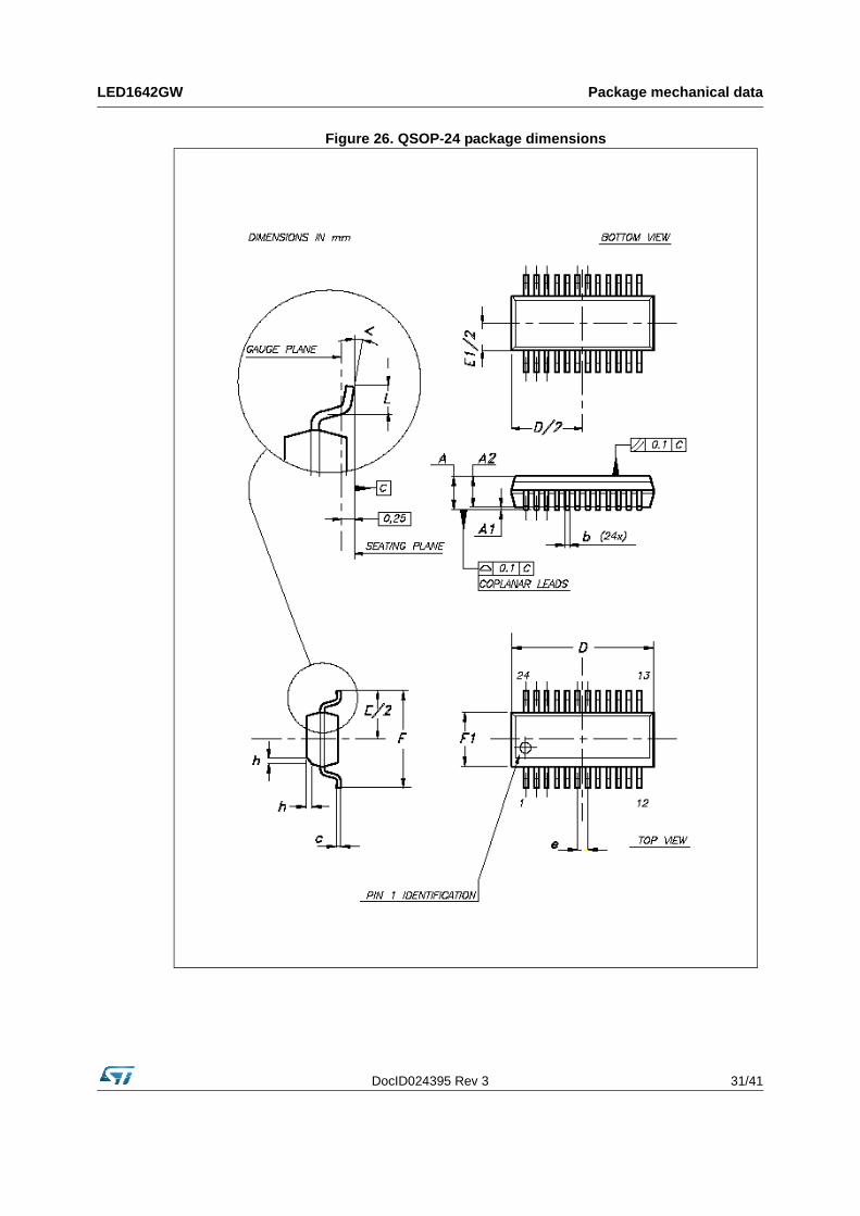
DocID024395 Rev 3 31/41
LED1642GW Package mechanical data
Figure 26. QSOP-24 package dimensions

Package mechanical data LED1642GW
32/41 DocID024395 Rev 3
Table 14. QFN-24 mechanical data
Dim.mm
Min. Typ. Max.
A 0.80 0.90 1.00
A1 0 0.02 0.05
A3 0.20
b 0.18 0.25 0.30
D 3.85 4.00 4.15
D2 2.00 2.15 2.25
E 3.85 4.00 4.15
E2 2.00 2.15 2.25
e 0.50
L 0.30 0.40 0.50

DocID024395 Rev 3 33/41
LED1642GW Package mechanical data
Figure 27. QFN-24 package dimensions

Package mechanical data LED1642GW
34/41 DocID024395 Rev 3
Figure 28. TSSOP24 package dimensions
Table 15. TSSOP24 mechanical data
Dim.mm
Min. Typ. Max.
A 1.1
A1 0.05 0.15
A2 0.9
b 0.19 0.30
c 0.09 0.20
D 7.7 7.9
E 4.3 4.5
e 0.65 BSC
H 6.25 6.5
K 0° 8°
L 0.50 0.70
DocID024395 Rev 3 35/41
LED1642GW Package mechanical data
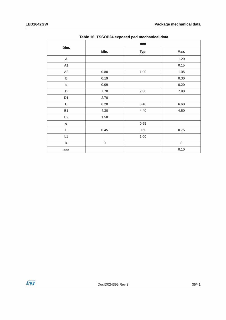
Table 16. TSSOP24 exposed pad mechanical data
Dim.mm
Min. Typ. Max.
A 1.20
A1 0.15
A2 0.80 1.00 1.05
b 0.19 0.30
c 0.09 0.20
D 7.70 7.80 7.90
D1 2.70
E 6.20 6.40 6.60
E1 4.30 4.40 4.50
E2 1.50
e 0.65
L 0.45 0.60 0.75
L1 1.00
k 0 8
aaa 0.10

Package mechanical data LED1642GW
36/41 DocID024395 Rev 3
Figure 29. TSSOP24 exposed pad dimensions
7100778_D

DocID024395 Rev 3 37/41
LED1642GW Packaging mechanical data
12 Packaging mechanical data
Table 17. TSSOP24 and TSSOP24 exposed pad tape and reel mechanical data
Dim.mm
Min. Typ. Max.
A - 330
C 12.8 - 13.2
D 20.2 -
N 60 -
T - 22.4
Ao 6.8 - 7
Bo 8.2 - 8.4
Ko 1.7 - 1.9
Po 3.9 - 4.1
P 11.9 - 12.1

Packaging mechanical data LED1642GW
38/41 DocID024395 Rev 3
Figure 30. TSSOP24 and TSSOP24 exposed pad tape and reel dimensions

DocID024395 Rev 3 39/41
LED1642GW Ordering information
13 Ordering information
Table 18. Ordering information
Order code Package Packaging
LED1642GWPTR QSOP-24 2500 parts per reel
LED1642GWQTR QFN-24 4000 parts per reel
LED1642GWTTR TSSOP24 2500 parts per reel
LED1642GWXTTR TSSOP24 exposed pad 2500 parts per reel

Revision history LED1642GW
40/41 DocID024395 Rev 3
14 Revision history
Table 19. Document revision history
Date Revision Changes
03-May-2013 1 Initial release.
06-Jun-2013 2
Updated Table 2: Absolute maximum ratings, Figure 10: Channel current vs. gain register value and Section 8.2: Error detection mode (CFG-7).Added Figure 13, 14, 15 and 16.
Minor text changes.
19-Aug-2013 3
Updated the Title, the Features and the Description.
Modified Table 4: Electrical characteristics, Updated Table 9: Example of current ranges, Table 10: Gain steps for the current range selected by REXT = 11 kW, Section 8.2: Error detection mode (CFG-7), Section 8.8: PWM counter setting and brightness register (CFG-15).

DocID024395 Rev 3 41/41
LED1642GW
Please Read Carefully:
Information in this document is provided solely in connection with ST products. STMicroelectronics NV and its subsidiaries (“ST”) reserve theright to make changes, corrections, modifications or improvements, to this document, and the products and services described herein at anytime, without notice.
All ST products are sold pursuant to ST’s terms and conditions of sale.
Purchasers are solely responsible for the choice, selection and use of the ST products and services described herein, and ST assumes noliability whatsoever relating to the choice, selection or use of the ST products and services described herein.
No license, express or implied, by estoppel or otherwise, to any intellectual property rights is granted under this document. If any part of thisdocument refers to any third party products or services it shall not be deemed a license grant by ST for the use of such third party productsor services, or any intellectual property contained therein or considered as a warranty covering the use in any manner whatsoever of suchthird party products or services or any intellectual property contained therein.
UNLESS OTHERWISE SET FORTH IN ST’S TERMS AND CONDITIONS OF SALE ST DISCLAIMS ANY EXPRESS OR IMPLIEDWARRANTY WITH RESPECT TO THE USE AND/OR SALE OF ST PRODUCTS INCLUDING WITHOUT LIMITATION IMPLIEDWARRANTIES OF MERCHANTABILITY, FITNESS FOR A PARTICULAR PURPOSE (AND THEIR EQUIVALENTS UNDER THE LAWSOF ANY JURISDICTION), OR INFRINGEMENT OF ANY PATENT, COPYRIGHT OR OTHER INTELLECTUAL PROPERTY RIGHT.
ST PRODUCTS ARE NOT AUTHORIZED FOR USE IN WEAPONS. NOR ARE ST PRODUCTS DESIGNED OR AUTHORIZED FOR USEIN: (A) SAFETY CRITICAL APPLICATIONS SUCH AS LIFE SUPPORTING, ACTIVE IMPLANTED DEVICES OR SYSTEMS WITHPRODUCT FUNCTIONAL SAFETY REQUIREMENTS; (B) AERONAUTIC APPLICATIONS; (C) AUTOMOTIVE APPLICATIONS ORENVIRONMENTS, AND/OR (D) AEROSPACE APPLICATIONS OR ENVIRONMENTS. WHERE ST PRODUCTS ARE NOT DESIGNEDFOR SUCH USE, THE PURCHASER SHALL USE PRODUCTS AT PURCHASER’S SOLE RISK, EVEN IF ST HAS BEEN INFORMED INWRITING OF SUCH USAGE, UNLESS A PRODUCT IS EXPRESSLY DESIGNATED BY ST AS BEING INTENDED FOR “AUTOMOTIVE,AUTOMOTIVE SAFETY OR MEDICAL” INDUSTRY DOMAINS ACCORDING TO ST PRODUCT DESIGN SPECIFICATIONS.PRODUCTS FORMALLY ESCC, QML OR JAN QUALIFIED ARE DEEMED SUITABLE FOR USE IN AEROSPACE BY THECORRESPONDING GOVERNMENTAL AGENCY.
Resale of ST products with provisions different from the statements and/or technical features set forth in this document shall immediately voidany warranty granted by ST for the ST product or service described herein and shall not create or extend in any manner whatsoever, anyliability of ST.
ST and the ST logo are trademarks or registered trademarks of ST in various countries.Information in this document supersedes and replaces all information previously supplied.
The ST logo is a registered trademark of STMicroelectronics. All other names are the property of their respective owners.
© 2013 STMicroelectronics - All rights reserved
STMicroelectronics group of companies
Australia - Belgium - Brazil - Canada - China - Czech Republic - Finland - France - Germany - Hong Kong - India - Israel - Italy - Japan - Malaysia - Malta - Morocco - Philippines - Singapore - Spain - Sweden - Switzerland - United Kingdom - United States of America
www.st.com