16-bit digital-to-analog converter with serial data ... · pdf filedac714 2 sbas032a pin...
TRANSCRIPT
www.ti.com
FEATURES: SERIAL DIGITAL INTERFACE
VOLTAGE OUTPUT: ±10V, ±5V, 0 to +10V
±1 LSB INTEGRAL LINEARITY
16-BIT MONOTONIC OVER TEMPERATURE
PRECISION INTERNAL REFERENCE
LOW NOISE: 120nV/√Hz Including Reference
16-LEAD PLASTIC AND CERAMIC SKINNYDIP AND PLASTIC SO PACKAGES
16-Bit DIGITAL-TO-ANALOG CONVERTERWith Serial Data Interface
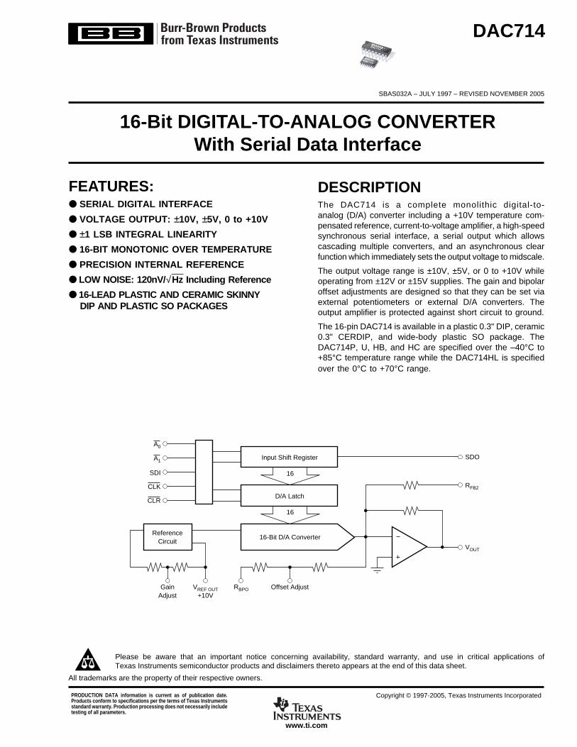
DESCRIPTIONThe DAC714 is a complete monolithic digital-to-analog (D/A) converter including a +10V temperature com-pensated reference, current-to-voltage amplifier, a high-speedsynchronous serial interface, a serial output which allowscascading multiple converters, and an asynchronous clearfunction which immediately sets the output voltage to midscale.
The output voltage range is ±10V, ±5V, or 0 to +10V whileoperating from ±12V or ±15V supplies. The gain and bipolaroffset adjustments are designed so that they can be set viaexternal potentiometers or external D/A converters. Theoutput amplifier is protected against short circuit to ground.
The 16-pin DAC714 is available in a plastic 0.3" DIP, ceramic0.3" CERDIP, and wide-body plastic SO package. TheDAC714P, U, HB, and HC are specified over the –40°C to+85°C temperature range while the DAC714HL is specifiedover the 0°C to +70°C range.
VOUT
VREF OUT+10V
ReferenceCircuit
16-Bit D/A Converter
D/A Latch
SDO
RFB2
16
Input Shift Register
16
A1
SDI
CLK
CLR
A0
Offset AdjustGainAdjust
RBPO
DAC714
SBAS032A – JULY 1997 – REVISED NOVEMBER 2005
PRODUCTION DATA information is current as of publication date.Products conform to specifications per the terms of Texas Instrumentsstandard warranty. Production processing does not necessarily includetesting of all parameters.
Copyright © 1997-2005, Texas Instruments Incorporated
Please be aware that an important notice concerning availability, standard warranty, and use in critical applications ofTexas Instruments semiconductor products and disclaimers thereto appears at the end of this data sheet.
All trademarks are the property of their respective owners.
DAC714
DAC714
DAC7142SBAS032Awww.ti.com
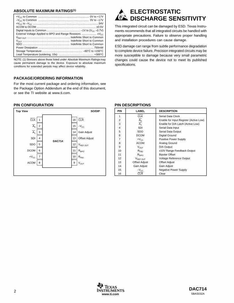
PIN CONFIGURATION
Top View
CLK
A0
A1
SDI
SDO
DCOM
+VCC
ACOM
DAC714
CLR
–VCC
Gain Adjust
Offset Adjust
VREF OUT
RBPO
RFB2
VOUT
1
2
3
4
5
6
7
8
16
15
14
13
12
11
10
9
PIN DESCRIPTIONSPIN LABEL DESCRIPTION
1 CLK Serial Data Clock2 A0 Enable for Input Register (Active Low)3 A1 Enable for D/A Latch (Active Low)4 SDI Serial Data Input5 SDO Serial Data Output6 DCOM Digital Ground7 +VCC Positive Power Supply8 ACOM Analog Ground9 VOUT D/A Output10 RFB2 ±10V Range Feedback Output11 RBPO Bipolar Offset12 VREF OUT Voltage Reference Output13 Offset Adjust Offset Adjust14 Gain Adjust Gain Adjust15 –VCC Negative Power Supply16 CLR Clear
SO/DIP
+VCC to Common .................................................................... 0V to +17V–VCC to Common .................................................................... 0V to –17V+VCC to –VCC ....................................................................................... 34VACOM to DCOM ............................................................................... ±0.5VDigital Inputs to Common ............................................. –1V to (VCC –0.7V)External Voltage Applied to BPO and Range Resistors .................... ±VCC
VREF OUT .......................................................... Indefinite Short to CommonVOUT ............................................................... Indefinite Short to CommonSDO ............................................................... Indefinite Short to CommonPower Dissipation .......................................................................... 750mWStorage Temperature ...................................................... –60°C to +150°CLead Temperature (soldering, 10s) ............................................... +300°C
NOTE: (1) Stresses above those listed under Absolute Maximum Ratings maycause permanent damage to the device. Exposure to absolute maximumconditions for extended periods may affect device reliability.
ABSOLUTE MAXIMUM RATINGS(1) ELECTROSTATICDISCHARGE SENSITIVITY
This integrated circuit can be damaged by ESD. Texas Instru-ments recommends that all integrated circuits be handled withappropriate precautions. Failure to observe proper handlingand installation procedures can cause damage.
ESD damage can range from subtle performance degradationto complete device failure. Precision integrated circuits may bemore susceptible to damage because very small parametricchanges could cause the device not to meet its publishedspecifications.
For the most current package and ordering information, seethe Package Option Addendum at the end of this document,or see the TI website at www.ti.com.
PACKAGE/ORDERING INFORMATION

DAC714 3SBAS032A www.ti.com
ELECTRICAL CHARACTERISTICSAt TA = +25°C, +VCC = +12V and +15V, –VCC = –12V, and –15V, unless otherwise noted.
Binary Two’s Complement
DAC714P, U DAC714HB DAC714HC DAC714HL
PARAMETER MIN TYP MAX MIN TYP MAX MIN TYP MAX MIN TYP MAX UNITS
TRANSFER CHARACTERISTICS
ACCURACYLinearity Error ±4 ±2 ±1 ±1 LSBTMIN to TMAX ±8 ±4 ±2 ±2 LSBDifferential Linearity Error ±4 ±2 ±1 ±1 LSBTMIN to TMAX ±8 ±4 ±2 ±1 LSBMonotonicity 14 15 16 16 BitsMonotonicity Over Spec Temp Range 13 14 15 16 BitsGain Error(3) ±0.1 ±0.1 ±0.1 ±0.1 %TMIN to TMAX ±0.25 ±0.25 ±0.25 ±0.25 %Unipolar/Bipolar Zero Error(3) ±0.1 ±0.1 ±0.1 ±0.1 % of FSR(2)
TMIN to TMAX ±0.2 ±0.2 ±0.2 ±0.2 % of FSRPower Supply Sensitivity of Gain ±0.003 ±0.003 ±0.003 ±0.003 %FSR/%VCC
±30 ±30 ±30 ±30 ppm FSR/%VCC
DYNAMIC PERFORMANCESettling Time(to ±0.003%FSR, 5kΩ || 500pF Load)(4)
20V Output Step 6 10 6 10 6 10 6 10 µs1LSB Output Step(5) 4 4 4 4 µsOutput Slew Rate 10 10 10 10 V/µsTotal Harmonic Distortion0dB, 1001Hz, fS = 100kHz 0.005 0.005 0.005 0.005 %–20dB, 1001Hz, fS = 100kHz 0.03 0.03 0.03 0.03 %–60dB, 1001Hz, fS = 100kHz 3.0 3.0 3.0 3.0 %SINAD: 1001Hz, fS = 100kHz 87 87 87 87 dBDigital Feedthrough(5) 2 2 2 2 nV–sDigital-to-Analog Glitch Impulse(5) 15 15 15 15 nV–sOutput Noise Voltage (includes reference) 120 120 120 120 nV/√Hz
ANALOG OUTPUTOutput Voltage Range+VCC, –VCC = ±11.4V ±10 ±10 ±10 ±10 VOutput Current ±5 ±5 ±5 ±5 mAOutput Impedance 0.1 0.1 0.1 0.1 ΩShort Circuit to ACOM Duration Indefinite Indefinite Indefinite Indefinite
REFERENCE VOLTAGEVoltage +9.975 +10.000 +10.025 +9.975 +10.000 +10.025 +9.975 +10.000 +10.025 +9.975 +10.000 +10.025 VTMIN to TMAX +9.960 +10.040 +9.960 +10.040 +9.960 +10.040 +9.960 +10.040 VOutput Resistance 1 1 1 1 ΩSource Current 2 2 2 2 mAShort Circuit to ACOM Duration Indefinite Indefinite Indefinite Indefinite
INTERFACE
RESOLUTION 16 16 16 16 BitsDIGITAL INPUTSSerial Data Input CodeLogic Levels(1)
VIH +2.0 (VCC –1.4) +2.0 (VCC –1.4) +2.0 (VCC –1.4) +2.0 (VCC –1.4) V
VIL 0 +0.8 0 +0.8 0 +0.8 0 +0.8 V
IIH (VI = +2.7V) ±10 ±10 ±10 ±10 µA
IIL (VI = +0.4V) ±10 ±10 ±10 ±10 µA
DIGITAL OUTPUTSerial DataVOL (ISINK = 1.6mA) 0 +0.4 0 +0.4 0 +0.4 0 +0.4 VVOH (ISOURCE = 500µA), TMIN to TMAX +2.4 +5 +2.4 +5 +2.4 +5 +2.4 +5 V
POWER SUPPLY REQUIREMENTSVoltage+VCC +11.4 +15 +16.5 +11.4 +15 +16.5 +11.4 +15 +16.5 +11.4 +15 +16.5 V–VCC –11.4 –15 –16.5 –11.4 –15 –16.5 –11.4 –15 –16.5 –11.4 –15 –16.5 VCurrent (No Load, ±15V Supplies)(6)
+VCC 13 16 13 16 13 16 13 16 mA–VCC 22 26 22 26 22 26 22 26 mAPower Dissipation(7) 625 625 625 625 mW
TEMPERATURE RANGESSpecificationAll Grades –40 +85 –40 +85 –40 +85 0 +70 °CStorage –60 +150 –60 +150 –60 +150 –60 +150 °CThermal Coefficient, θJA 75 75 75 75 °C/W
NOTES: (1) Digital inputs are TTL and +5V CMOS compatible over the specification temperature range. (2) FSR means Full Scale Range. For example, for ±10V output, FSR = 20V. (3) Errorsexternally adjustable to zero. (4) Maximum represents the 3σ limit. Not 100% tested for this parameter. (5) For the worst-case Binary Two’s Complement code changes: FFFFH to 0000H and 0000H
to FFFFH. (6) During power supply turn on, the transient supply current may approach 3x the maximum quiescent specification. (7) Typical (i.e. rated) supply voltages times maximum currents.

DAC7144SBAS032Awww.ti.com
CLK
A0
SDISerial Data Input
MSB First
Latch DataIn D/A Latch
A1
tA0H
D0D14D15
tA1S tA1H
tDHtDS
tA0S
tCLK
tCH tCL
CLK
A0
SDOSerial Data
Out
tA0S tA0H
D0D14
Clear
D15
tCLK
tCH tCL
CLR
tDSOP
tCP
tDSOP
TIMING SPECIFICATIONSTA = –40°C to +85°C, +VCC = +12V or +15V, –VCC = –12V or –15V.
SYMBOL PARAMETER MIN MAX UNITS
tCLK Data Clock Period 100 nstCL Clock LOW 50 nstCH Clock HIGH 50 nstA0S Setup Time for A0 50 nstA1S Setup Time for A1 50 nstAOH Hold Time for A0 0 nstA1H Hold Time for A1 0 nstDS Setup Time for DATA 50 nstDH Hold Time for DATA 10 ns
tDSOP Output Propagation Delay 140 nstCP Clear Pulsewidth 200 ns
A0 A1 CLK CLR DESCRIPTION
0 1 1 → 0 → 1 1 Shift Serial Data into SDI
1 0 1 → 0 → 1 1 Load D/A Latch
1 1 1 → 0 → 1 1 No Change
0 0 1 → 0 → 1 1 Two Wire Operation(1)
X X 1 1 No Change
X X X 0 Reset D/A Latch
NOTES: X = Don’t Care. (1) All digital input changes will appear at theoutput.
TRUTH TABLE
TIMING DIAGRAMS
Serial Data In
Serial Data Out

DAC714 5SBAS032A www.ti.com
Time (10µs/div)
± FULL SCALE OUTPUT SWING
V
(
V)
OU
T
0
10
–10
Frequency (Hz)
[Cha
nge
in F
SR
] / [C
hang
e in
Sup
ply
Vol
tage
]
1k
10 100 1k 10k 100k 1M
POWER SUPPLY REJECTION vsPOWER SUPPLY RIPPLE FREQUENCY
(ppm
of F
SR
/ %)
100
10
1
0.1
–VCC
+VCC
TYPICAL CHARACTERISTICSAt TA = +25°C, VCC = ±15V, unless otherwise noted.
A1
(V)
SETTLING TIME, +10V TO –10V
Time (1µs/div)
2500
2000
1500
1000
500
0
–500
–1000
–1500
–2000
–2500
∆ A
roun
d –1
0V (
µV)
+5V
0V
A1
SETTLING TIME, –10V TO +10V
Time (1µs/div)
2500
2000
1500
1000
500
0
–500
–1000
–1500
–2000
–2500
∆ A
roun
d +
10V
(µV
)
+5V
0V
1000
100
10
11 10 100 1k 10k 100k 1M 10M
Frequency (Hz)
nV/√
Hz
VOUT SPECTRAL NOISE DENSITY
2.0
–0.85 0 2.55 4.25 5.95 6.8
LOGIC vs V LEVEL
1.0
0
–1.0
–2.00.85 1.7 3.4 5.1
SDI
A0, A1
CLR
V Digital Input
I Dig
ital I
nput
(µA
)

DAC7146SBAS032Awww.ti.com
DISCUSSION OFSPECIFICATIONSLINEARITY ERROR
Linearity error is defined as the deviation of the analogoutput from a straight line drawn between the end points ofthe transfer characteristic.
DIFFERENTIAL LINEARITY ERROR
Differential linearity error (DLE) is the deviation from1LSB of an output change from one adjacent state to thenext. A DLE specification of ±1/2LSB means that the outputstep size can range from 1/2LSB to 3/2LSB when the digitalinput code changes from one code word to the adjacent codeword. If the DLE is more positive than –1LSB, the D/A issaid to be monotonic.
MONOTONICITY
A D/A converter is monotonic if the output either increasesor remains the same for increasing digital input values.Monotonicity of the C and L grades is assured over thespecification temperature range to 16 bits.
SETTLING TIME
Settling time is the total time (including slew time) for theD/A output to settle to within an error band around its finalvalue after a change in input. Settling times are specified towithin ±0.003% of Full Scale Range (FSR) for an outputstep change of 20V and 1LSB. The 1LSB change is mea-sured at the Major Carry (FFFFH to 0000H, and 0000H toFFFFH: BTC codes), the input transition at which worst-casesettling time occurs.
TOTAL HARMONIC DISTORTION
Total harmonic distortion is defined as the ratio of thesquare root of the sum of the squares of the values of theharmonics to the value of the fundamental frequency. It isexpressed in % of the fundamental frequency amplitude atsampling rate fS.
SIGNAL-TO-NOISEAND DISTORTION RATIO (SINAD)
SINAD includes all the harmonic and outstanding spuriouscomponents in the definition of output noise power inaddition to quantizing and internal random noise power.SINAD is expressed in dB at a specified input frequency andsampling rate, fS.
DIGITAL-TO-ANALOG GLITCH IMPULSE
The amount of charge injected into the analog output fromthe digital inputs when the inputs change state. It is mea-sured at half scale at the input codes where as many aspossible switches change state—from 0000H to FFFFH.
DIGITAL FEEDTHROUGH
When the A/D is not selected, high frequency logic activityon the digital inputs is coupled through the device and showsup as output noise. This noise is digital feedthrough.
OPERATIONThe DAC714 is a monolithic integrated-circuit 16-bit D/Aconverter complete with 16-bit D/A switches and laddernetwork, voltage reference, output amplifier and a serialinterface.
INTERFACE LOGIC
The DAC714 has double-buffered data latches. The inputdata latch holds a 16-bit data word before loading it into thesecond latch, the D/A latch. This double-buffered organiza-tion permits simultaneous update of several D/A converters.All digital control inputs are active low. Refer to the blockdiagram shown in Figure 1.
All latches are level-triggered. Data present when the enableinputs are logic “0” will enter the latch. When the enableinputs return to logic “1”, the data is latched.
The CLR input resets both the input latch and the D/A latchto 0000H (midscale).
LOGIC INPUT COMPATIBILITY
The DAC714 digital inputs are TTL compatible (1.4V switch-ing level), low leakage, and high impedance. Thus, theinputs are suitable for being driven by any type of 5V logicfamily, such as CMOS. An equivalent circuit for the digitalinputs is shown in Figure 2.
The inputs will float to logic “0” if left unconnected. It isrecommended that any unused inputs be connected to DCOMto improve noise immunity.
Digital inputs remain high impedance when power is off.
INPUT CODING
The DAC714 is designed to accept binary two’s comple-ment (BTC) input codes with the MSB first which arecompatible with bipolar analog output operation. For thisconfiguration, a digital input of 7FFFH produces a plus fullscale output, 8000H produces a minus full scale output, and0000H produces bipolar zero output.
INTERNAL REFERENCE
The DAC714 contains a +10V reference. The referenceoutput may be used to drive external loads, sourcing up to2mA. The load current should be constant; otherwise, thegain and bipolar offset of the converter will vary.
DAC714 7SBAS032A www.ti.com
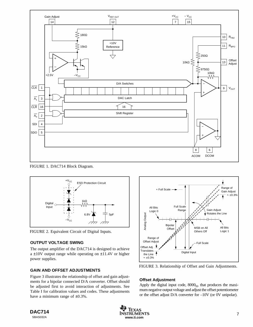
FIGURE 1. DAC714 Block Diagram.
OUTPUT VOLTAGE SWING
The output amplifier of the DAC714 is designed to achievea ±10V output range while operating on ±11.4V or higherpower supplies.
GAIN AND OFFSET ADJUSTMENTS
Figure 3 illustrates the relationship of offset and gain adjust-ments for a bipolar connected D/A converter. Offset shouldbe adjusted first to avoid interaction of adjustments. SeeTable I for calibration values and codes. These adjustmentshave a minimum range of ±0.3%.
FIGURE 3. Relationship of Offset and Gain Adjustments.
Offset AdjustmentApply the digital input code, 8000H, that produces the maxi-mum negative output voltage and adjust the offset potentiometeror the offset adjust D/A converter for –10V (or 0V unipolar).
Shift Register
DAC Latch
14 12
+10VReference
8 6
7
DCOM
+VCC
ACOM
VREF OUTGain Adjust
4SDI
5SDO
16
2A0
3A1
1
16
CLK
CLR
15
– VCC
OffsetAdjust13
RBPO11
RFB210
9 VOUT
D/A Switches
–VCC+2.5V
15kΩ
180Ω
9750Ω
250Ω
10kΩ
10kΩ
FIGURE 2. Equivalent Circuit of Digital Inputs.
1kΩ
ESD Protection Circuit
6.8V 5pF
DigitalInput
–VCC
+VCC
+ Full Scale
All BitsLogic 0
Range ofOffset Adjust
Offset Adj.Translates
the LineDigital Input
All BitsLogic 1
Ana
log
Out
put
Full ScaleRange Gain Adjust
Rotates the Line
– Full Scale
MSB on AllOthers Off
BipolarOffset
Range ofGain Adjust
≈ ±0.3%
≈ ±0.3%

DAC7148SBAS032Awww.ti.com
DAC714 CALIBRATION VALUES
DIGITAL INPUT CODE ANALOG OUTPUT (V)BINARY TWO’S BIPOLAR UNIPOLAR
COMPLEMENT, BTC 20V RANGE 10V RANGE DESCRIPTION
7FFFH +9.999695 +9.999847 + Full Scale –1LSB|
4000H +5.000000 +7.500000 3/4 Scale|
0001H +0.000305 +5.000153 BPZ + 1LSB
0000H 0.000000 +5.000000 Bipolar Zero (BPZ)
FFFFH –0.000305 +4.999847 BPZ – 1LSB|
C000H –5.000000 +2.500000 1/4 Scale|
8000H –10.00000 0.000000 Minus Full Scale
critical settling time may be able to use 0.01µF at –VCCas well as at +VCC. The capacitors should be locatedclose to the package.
The DAC714 has separate ANALOG COMMON and DIGI-TAL COMMON pins. The current through DCOM is mostlyswitching transients and are up to 1mA peak in amplitude.The current through ACOM is typically 5µA for all codes.
Use separate analog and digital ground planes with a singleinterconnection point to minimize ground loops. The analogpins are located adjacent to each other to help isolate analogfrom digital signals. Analog signals should be routed as faras possible from digital signals and should cross them atright angles. A solid analog ground plane around the D/Apackage, as well as under it in the vicinity of the analog andpower supply pins, will isolate the D/A from switchingcurrents. It is recommended that DCOM and ACOM beconnected directly to the ground planes under the package.
If several DAC714s are used or if DAC714 shares supplieswith other components, connecting the ACOM and DCOMlines to together once at the power supplies rather than ateach chip may give better results.
LOAD CONNECTIONS
Since the reference point for VOUT and VREF OUT is theACOM pin, it is important to connect the D/A converter loaddirectly to the ACOM pin. Refer to Figure 5.
Lead and contact resistances are represented by R1 throughR3. As long as the load resistance RL is constant, R1 simplyintroduces a gain error and can be removed by gain adjust-ment of the D/A or system-wide gain calibration. R2 is partof RL if the output voltage is sensed at ACOM.
In some applications it is impractical to return the load to theACOM pin of the D/A converter. Sensing the output voltageat the SYSTEM GROUND point is reasonable, because thereis no change in DAC714 ACOM current, provided that R3 isa low-resistance ground plane or conductor. In this case youmay wish to connect DCOM to SYSTEM GROUND as well.
FIGURE 4. Power Supply Connections.
1
2
3
4
5
6
7
8
16
15
14
13
12
11
10
9
1µF
1µF
DAC714
DCOM
+VCC
ACOM
−VCC
+12V to +15V
−12V to −15V
+
+
TABLE I. Digital Input and Analog Output Voltage Calibra-tion Values.
Gain Adjustment
Apply the digital input that gives the maximum positivevoltage output. Adjust the gain potentiometer or the gainadjust D/A converter for this positive full scale voltage.
INSTALLATIONGENERAL CONSIDERATIONS
Due to the high accuracy of the DAC714 system design,problems such as grounding and contact resistance becomevery important. A 16-bit converter with a 20V full-scalerange has a 1LSB value of 305µV. With a load current of5mA, series wiring and connector resistance of only 60mΩwill cause a voltage drop of 300µV. To understand what thismeans in terms of a system layout, the resistivity of a typical1 ounce copper-clad printed circuit board is 1/2 mΩ persquare. For a 5mA load, a 10 milliinch wide printed circuitconductor 60 milliinches long will result in a voltage drop of150µV.
The analog output of DAC714 has an LSB size of 305µV(–96dB) in the bipolar mode. The rms noise floor of the D/Ashould remain below this level in the frequency range ofinterest. The DAC714’s output noise spectral density (whichincludes the noise contributed by the internal reference,) isshown in the Typical Characteristic section.
Wiring to high-resolution D/A converters should be routedto provide optimum isolation from sources of RFI and EMI.The key to elimination of RF radiation or pickup is smallloop area. Signal leads and their return conductors should bekept close together such that they present a small capturecross-section for any external field. Wire-wrap constructionis not recommended.
POWER SUPPLY ANDREFERENCE CONNECTIONS
Power supply decoupling capacitors should be added asshown in Figure 4. Best performance occurs using a 1 to10µF tantalum capacitor at –VCC. Applications with less

DAC714 9SBAS032A www.ti.com
DIGITAL INTERFACESERIAL INTERFACE
The DAC714 has a serial interface with two data bufferswhich can be used for either synchronous or asynchronousupdating of multiple D/A converters. A0 is the enable controlfor the input shift register. A1 is the enable for the D/A Latch.CLK is used to strobe data into the latches enabled by A0 andA1. A CLR function is also provided and when enabled it setsthe shift register and the D/A Latch to 0000H (output voltageis midscale).
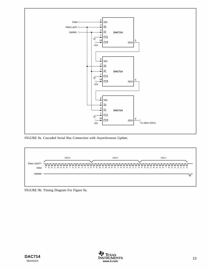
Multiple DAC714s can be connected to the same CLK anddata lines in two ways. The output of the serial shift registeris available as SDO so that any number of DAC714s can becascaded on the same input bit stream as shown in Figures8 and 9. This configuration allows all D/A converters to beupdated simultaneously and requires a minimum number ofcontrol signals. These configurations do require 16N CLKcycles to load any given D/A converter, where N is thenumber of D/A converters.
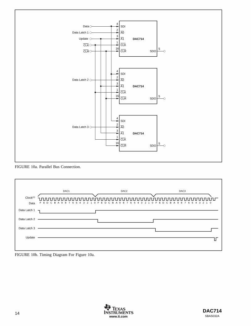
The DAC714 can also be connected in parallel as shown inFigure 10. This configuration allows any D/A converter inthe system to be updated in a maximum of 16 CLK cycles.
GAIN AND OFFSET ADJUST
Connections Using Potentiometers
GAIN and OFFSET adjust pins provide for trim usingexternal potentiometers. 15-turn potentiometers provide suf-ficient resolution. Range of adjustment of these trims is atleast ±0.3% of Full Scale Range. Refer to Figure 6.
Using D/A Converters
The GAIN ADJUST and OFFSET ADJUST circuits ofthe DAC714 have been arranged so that these points maybe easily driven by external D/A converters. Refer toFigure 7. 12-bit D/A converters provide an OFFSETadjust resolution and a GAIN adjust resolution of 30µVto 50µV per LSB step.
Nominal values of GAIN and OFFSET occur when the D/Aconverters outputs are at approximately half scale, +5V.
OUTPUT VOLTAGE RANGE CONNECTIONS
The DAC714 output amplifier is connected internally toprovide a 20V output range. For other ranges and configu-rations, see Figures 6 and 7.
FIGURE 5. System Ground Considerations for High-Resolution D/A Converters.
R1
SenseOutput
RL
R2
R3
Alternate GroundSense Connection
System Ground
ACOMDCOM
BusInterface
DAC714
AnalogPowerSupply
0.01µF(1)
0.01µF
To +VCC
To –VCC
NOTE: (1) Locate close to DAC714 package.
VOUT
10kΩ10kΩVREF
VREF RBPO
SDI
A0
A1
CLR
10kΩRFB2

DAC71410SBAS032Awww.ti.com
FIGURE 6a. Manual Offset and Gain Adjust Circuits; Unipolar Mode (0V to +10V output range).
FIGURE 6b. Manual Offset and Gain Adjust Circuits; Bipolar Mode (–5V to +5V output range).
10kΩ
9
13
14
9.75kΩ
IDAC0-2mA
15kΩ
R327kΩ
R410kΩ
P11kΩ
P21kΩ
12
11
180Ω 250Ω
Internal+10V Reference VREF OUT
Gain Adjust
Bipolar Offset
Offset Adjust
8 ACOM
10kΩ10
RFB2
For no external adjustments, pins 13 and 14 are not connected. External resistors R1 - R4 are standard ±1% values. Range of adjustment at least ±0.3% FSR.
VOUT
R1100Ω
R2100Ω
10kΩ
10kΩ
R22MΩ
9
13
10
14
9.75kΩ
IDAC0-2mA
15kΩ
R327kΩ
R1100Ω +VCC
–VCC
VOUT
P11kΩ
12
180Ω
10kΩ to 100kΩ
Internal+10V Reference VREF OUT
Gain Adjust
Offset Adjust
8 ACOM
RFB2
For no external adjustments, pins 13 and 14 are not connected. External resistors R1 - R3 are standard ±1% values. Range of adjustment at least ±0.3% FSR.
DAC714 11SBAS032A www.ti.com
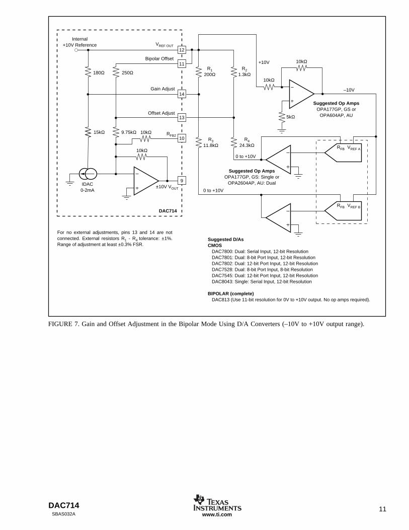
FIGURE 7. Gain and Offset Adjustment in the Bipolar Mode Using D/A Converters (–10V to +10V output range).
10kΩ
9
13
10
14
11
±10V VOUT
DAC714
9.75kΩ
IDAC0-2mA
15kΩR3
11.8kΩ
0 to +10V
R424.3kΩ
180Ω 250Ω
Internal+10V Reference VREF OUT
Gain Adjust
Offset Adjust
R1200Ω
R21.3kΩ
RFB VREF A
12
Suggested Op AmpsOPA177GP, GS or
OPA604AP, AU
RFB VREF B
0 to +10V
Suggested Op AmpsOPA177GP, GS: Single or
OPA2604AP, AU: Dual
5kΩ
10kΩ
+10V 10kΩ
–10V
Suggested D/AsCMOS
DAC7800: Dual: Serial Input, 12-bit ResolutionDAC7801: Dual: 8-bit Port Input, 12-bit ResolutionDAC7802: Dual: 12-bit Port Input, 12-bit ResolutionDAC7528: Dual: 8-bit Port Input, 8-bit ResolutionDAC7545: Dual: 12-bit Port Input, 12-bit ResolutionDAC8043: Single: Serial Input, 12-bit Resolution
BIPOLAR (complete)DAC813 (Use 11-bit resolution for 0V to +10V output. No op amps required).
10kΩ RFB2
Bipolar Offset
For no external adjustments, pins 13 and 14 are not connected. External resistors R1 - R4 tolerance: ±1%. Range of adjustment at least ±0.3% FSR.

DAC71412SBAS032Awww.ti.com
FIGURE 8a. Cascaded Serial Bus Connection with Synchronous Update.
FIGURE 8b. Timing Diagram For Figure 8a.
SDI
A0
A1
CLK
CLR
DAC714
SDO
Data
Data Latch
Update
CLK
4
2
3
1
16+5V
SDI
A0
A1
CLK
CLR
DAC714
SDO
4
2
3
1
16+5V
SDI
A0
A1
CLK
CLR
DAC714
SDO
4
2
3
1
16+5V
5
5
5
To other DACs
F E D C B A 9 8 7 6 5 4 3 2 1 0 F E D C B A 9 8 7 6 5 4 3 2 1 0 F E D C B A 9 8 7 6 5 4 3 2 1 0
Clock(1)
Data
Data Latch
Update
DAC3 DAC2 DAC1
DAC714 13SBAS032A www.ti.com
FIGURE 9a. Cascaded Serial Bus Connection with Asynchronous Update.
FIGURE 9b. Timing Diagram For Figure 9a.
SDI
A0
A1
CLK
CLR
DAC714
SDO
Data
Data Latch
Update
4
2
3
1
16
+5V
SDI
A0
A1
CLK
CLR
DAC714
SDO
4
2
3
1
16
+5V
SDI
A0
A1
CLK
CLR
DAC714
SDO
4
2
3
1
16
+5V
5
5
5
To other DACs
F E D C B A 9 8 7 6 5 4 3 2 1 0 F E D C B A 9 8 7 6 5 4 3 2 1 0 F E D C B A 9 8 7 6 5 4 3 2 1 0
Update
DAC3 DAC2 DAC1
Data Latch(1)
Data
DAC71414SBAS032Awww.ti.com
FIGURE 10a. Parallel Bus Connection.
FIGURE 10b. Timing Diagram For Figure 10a.
SDI
A0
A1
CLK
CLR
DAC714
SDO
Data
Data Latch 1
Data Latch 2
Data Latch 3
Update
CLK
4
2
3
1
16
SDI
A0
A1
CLK
CLR
DAC714
SDO
4
2
3
1
16
SDI
A0
A1
CLK
CLR
DAC714
SDO
4
2
3
1
16
5
5
5
CLR
F E D C B A 9 8 7 6 5 4 3 2 1 0 F E D C B A 9 8 7 6 5 4 3 2 1 0 F E D C B A 9 8 7 6 5 4 3 2 1 0
Clock(1)
Data
Data Latch 1
Data Latch 2
Data Latch 3
Update
DAC1 DAC2 DAC3
PACKAGE OPTION ADDENDUM
www.ti.com 15-Apr-2017
Addendum-Page 1
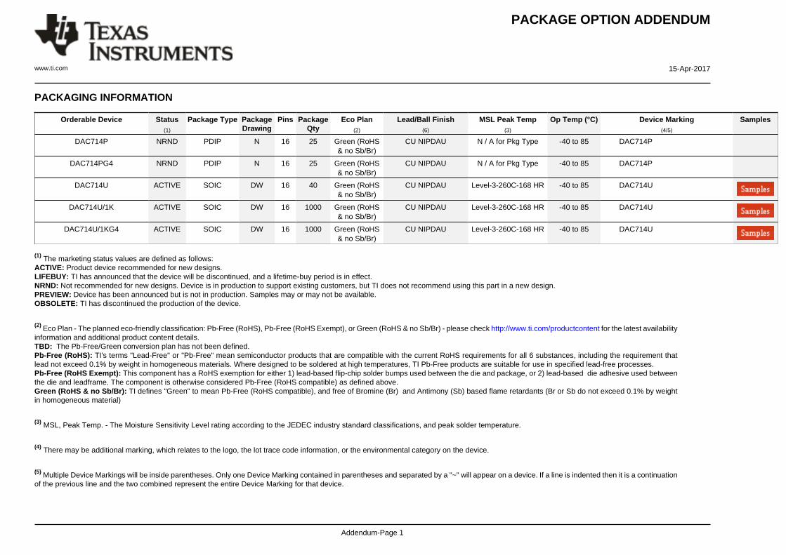
PACKAGING INFORMATION
Orderable Device Status(1)
Package Type PackageDrawing
Pins PackageQty
Eco Plan(2)
Lead/Ball Finish(6)
MSL Peak Temp(3)
Op Temp (°C) Device Marking(4/5)
Samples
DAC714P NRND PDIP N 16 25 Green (RoHS& no Sb/Br)
CU NIPDAU N / A for Pkg Type -40 to 85 DAC714P
DAC714PG4 NRND PDIP N 16 25 Green (RoHS& no Sb/Br)
CU NIPDAU N / A for Pkg Type -40 to 85 DAC714P
DAC714U ACTIVE SOIC DW 16 40 Green (RoHS& no Sb/Br)
CU NIPDAU Level-3-260C-168 HR -40 to 85 DAC714U
DAC714U/1K ACTIVE SOIC DW 16 1000 Green (RoHS& no Sb/Br)
CU NIPDAU Level-3-260C-168 HR -40 to 85 DAC714U
DAC714U/1KG4 ACTIVE SOIC DW 16 1000 Green (RoHS& no Sb/Br)
CU NIPDAU Level-3-260C-168 HR -40 to 85 DAC714U
(1) The marketing status values are defined as follows:ACTIVE: Product device recommended for new designs.LIFEBUY: TI has announced that the device will be discontinued, and a lifetime-buy period is in effect.NRND: Not recommended for new designs. Device is in production to support existing customers, but TI does not recommend using this part in a new design.PREVIEW: Device has been announced but is not in production. Samples may or may not be available.OBSOLETE: TI has discontinued the production of the device.
(2) Eco Plan - The planned eco-friendly classification: Pb-Free (RoHS), Pb-Free (RoHS Exempt), or Green (RoHS & no Sb/Br) - please check http://www.ti.com/productcontent for the latest availabilityinformation and additional product content details.TBD: The Pb-Free/Green conversion plan has not been defined.Pb-Free (RoHS): TI's terms "Lead-Free" or "Pb-Free" mean semiconductor products that are compatible with the current RoHS requirements for all 6 substances, including the requirement thatlead not exceed 0.1% by weight in homogeneous materials. Where designed to be soldered at high temperatures, TI Pb-Free products are suitable for use in specified lead-free processes.Pb-Free (RoHS Exempt): This component has a RoHS exemption for either 1) lead-based flip-chip solder bumps used between the die and package, or 2) lead-based die adhesive used betweenthe die and leadframe. The component is otherwise considered Pb-Free (RoHS compatible) as defined above.Green (RoHS & no Sb/Br): TI defines "Green" to mean Pb-Free (RoHS compatible), and free of Bromine (Br) and Antimony (Sb) based flame retardants (Br or Sb do not exceed 0.1% by weightin homogeneous material)
(3) MSL, Peak Temp. - The Moisture Sensitivity Level rating according to the JEDEC industry standard classifications, and peak solder temperature.
(4) There may be additional marking, which relates to the logo, the lot trace code information, or the environmental category on the device.
(5) Multiple Device Markings will be inside parentheses. Only one Device Marking contained in parentheses and separated by a "~" will appear on a device. If a line is indented then it is a continuationof the previous line and the two combined represent the entire Device Marking for that device.
PACKAGE OPTION ADDENDUM
www.ti.com 15-Apr-2017
Addendum-Page 2
(6) Lead/Ball Finish - Orderable Devices may have multiple material finish options. Finish options are separated by a vertical ruled line. Lead/Ball Finish values may wrap to two lines if the finishvalue exceeds the maximum column width.
Important Information and Disclaimer:The information provided on this page represents TI's knowledge and belief as of the date that it is provided. TI bases its knowledge and belief on informationprovided by third parties, and makes no representation or warranty as to the accuracy of such information. Efforts are underway to better integrate information from third parties. TI has taken andcontinues to take reasonable steps to provide representative and accurate information but may not have conducted destructive testing or chemical analysis on incoming materials and chemicals.TI and TI suppliers consider certain information to be proprietary, and thus CAS numbers and other limited information may not be available for release.
In no event shall TI's liability arising out of such information exceed the total purchase price of the TI part(s) at issue in this document sold by TI to Customer on an annual basis.
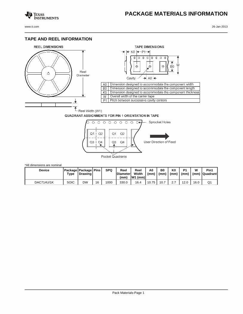
TAPE AND REEL INFORMATION
*All dimensions are nominal
Device PackageType
PackageDrawing
Pins SPQ ReelDiameter
(mm)
ReelWidth
W1 (mm)
A0(mm)
B0(mm)
K0(mm)
P1(mm)
W(mm)
Pin1Quadrant
DAC714U/1K SOIC DW 16 1000 330.0 16.4 10.75 10.7 2.7 12.0 16.0 Q1
PACKAGE MATERIALS INFORMATION
www.ti.com 26-Jan-2013
Pack Materials-Page 1

*All dimensions are nominal
Device Package Type Package Drawing Pins SPQ Length (mm) Width (mm) Height (mm)
DAC714U/1K SOIC DW 16 1000 367.0 367.0 38.0
PACKAGE MATERIALS INFORMATION
www.ti.com 26-Jan-2013
Pack Materials-Page 2

GENERIC PACKAGE VIEW
Images above are just a representation of the package family, actual package may vary.Refer to the product data sheet for package details.
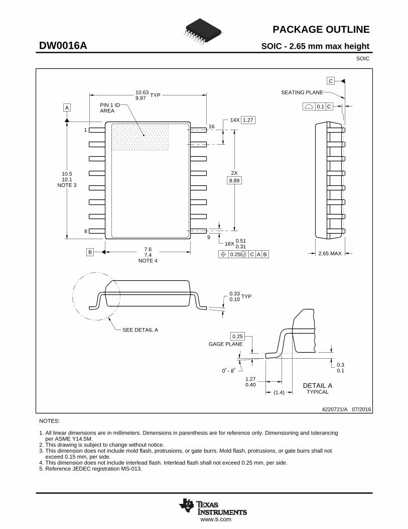
DW 16 SOIC - 2.65 mm max heightSMALL OUTLINE INTEGRATED CIRCUIT
4040000-2/H
www.ti.com
PACKAGE OUTLINE
C
TYP10.639.97
2.65 MAX
14X 1.27
16X 0.510.31
2X8.89
TYP0.330.10
0 - 80.30.1
(1.4)
0.25GAGE PLANE
1.270.40
A
NOTE 3
10.510.1
BNOTE 4
7.67.4
4220721/A 07/2016
SOIC - 2.65 mm max heightDW0016ASOIC
NOTES: 1. All linear dimensions are in millimeters. Dimensions in parenthesis are for reference only. Dimensioning and tolerancing per ASME Y14.5M. 2. This drawing is subject to change without notice. 3. This dimension does not include mold flash, protrusions, or gate burrs. Mold flash, protrusions, or gate burrs shall not exceed 0.15 mm, per side. 4. This dimension does not include interlead flash. Interlead flash shall not exceed 0.25 mm, per side.5. Reference JEDEC registration MS-013.
1 16
0.25 C A B
98
PIN 1 IDAREA
SEATING PLANE
0.1 C
SEE DETAIL A
DETAIL ATYPICAL
SCALE 1.500

www.ti.com
EXAMPLE BOARD LAYOUT
0.07 MAXALL AROUND
0.07 MINALL AROUND
(9.3)
14X (1.27)
R0.05 TYP
16X (2)
16X (0.6)
4220721/A 07/2016
SOIC - 2.65 mm max heightDW0016ASOIC
NOTES: (continued) 6. Publication IPC-7351 may have alternate designs. 7. Solder mask tolerances between and around signal pads can vary based on board fabrication site.
METAL SOLDER MASKOPENING
NON SOLDER MASKDEFINED
SOLDER MASK DETAILS
OPENINGSOLDER MASK METAL
SOLDER MASKDEFINED
LAND PATTERN EXAMPLESCALE:7X
SYMM
1
8 9
16
SEEDETAILS
SYMM

www.ti.com
EXAMPLE STENCIL DESIGN
R0.05 TYP
16X (2)
16X (0.6)
14X (1.27)
(9.3)
4220721/A 07/2016
SOIC - 2.65 mm max heightDW0016ASOIC
NOTES: (continued) 8. Laser cutting apertures with trapezoidal walls and rounded corners may offer better paste release. IPC-7525 may have alternate design recommendations. 9. Board assembly site may have different recommendations for stencil design.
SOLDER PASTE EXAMPLEBASED ON 0.125 mm THICK STENCIL
SCALE:7X
SYMM
SYMM
1
8 9
16


IMPORTANT NOTICE
Texas Instruments Incorporated (TI) reserves the right to make corrections, enhancements, improvements and other changes to itssemiconductor products and services per JESD46, latest issue, and to discontinue any product or service per JESD48, latest issue. Buyersshould obtain the latest relevant information before placing orders and should verify that such information is current and complete.TI’s published terms of sale for semiconductor products (http://www.ti.com/sc/docs/stdterms.htm) apply to the sale of packaged integratedcircuit products that TI has qualified and released to market. Additional terms may apply to the use or sale of other types of TI products andservices.Reproduction of significant portions of TI information in TI data sheets is permissible only if reproduction is without alteration and isaccompanied by all associated warranties, conditions, limitations, and notices. TI is not responsible or liable for such reproduceddocumentation. Information of third parties may be subject to additional restrictions. Resale of TI products or services with statementsdifferent from or beyond the parameters stated by TI for that product or service voids all express and any implied warranties for theassociated TI product or service and is an unfair and deceptive business practice. TI is not responsible or liable for any such statements.Buyers and others who are developing systems that incorporate TI products (collectively, “Designers”) understand and agree that Designersremain responsible for using their independent analysis, evaluation and judgment in designing their applications and that Designers havefull and exclusive responsibility to assure the safety of Designers' applications and compliance of their applications (and of all TI productsused in or for Designers’ applications) with all applicable regulations, laws and other applicable requirements. Designer represents that, withrespect to their applications, Designer has all the necessary expertise to create and implement safeguards that (1) anticipate dangerousconsequences of failures, (2) monitor failures and their consequences, and (3) lessen the likelihood of failures that might cause harm andtake appropriate actions. Designer agrees that prior to using or distributing any applications that include TI products, Designer willthoroughly test such applications and the functionality of such TI products as used in such applications.TI’s provision of technical, application or other design advice, quality characterization, reliability data or other services or information,including, but not limited to, reference designs and materials relating to evaluation modules, (collectively, “TI Resources”) are intended toassist designers who are developing applications that incorporate TI products; by downloading, accessing or using TI Resources in anyway, Designer (individually or, if Designer is acting on behalf of a company, Designer’s company) agrees to use any particular TI Resourcesolely for this purpose and subject to the terms of this Notice.TI’s provision of TI Resources does not expand or otherwise alter TI’s applicable published warranties or warranty disclaimers for TIproducts, and no additional obligations or liabilities arise from TI providing such TI Resources. TI reserves the right to make corrections,enhancements, improvements and other changes to its TI Resources. TI has not conducted any testing other than that specificallydescribed in the published documentation for a particular TI Resource.Designer is authorized to use, copy and modify any individual TI Resource only in connection with the development of applications thatinclude the TI product(s) identified in such TI Resource. NO OTHER LICENSE, EXPRESS OR IMPLIED, BY ESTOPPEL OR OTHERWISETO ANY OTHER TI INTELLECTUAL PROPERTY RIGHT, AND NO LICENSE TO ANY TECHNOLOGY OR INTELLECTUAL PROPERTYRIGHT OF TI OR ANY THIRD PARTY IS GRANTED HEREIN, including but not limited to any patent right, copyright, mask work right, orother intellectual property right relating to any combination, machine, or process in which TI products or services are used. Informationregarding or referencing third-party products or services does not constitute a license to use such products or services, or a warranty orendorsement thereof. Use of TI Resources may require a license from a third party under the patents or other intellectual property of thethird party, or a license from TI under the patents or other intellectual property of TI.TI RESOURCES ARE PROVIDED “AS IS” AND WITH ALL FAULTS. TI DISCLAIMS ALL OTHER WARRANTIES ORREPRESENTATIONS, EXPRESS OR IMPLIED, REGARDING RESOURCES OR USE THEREOF, INCLUDING BUT NOT LIMITED TOACCURACY OR COMPLETENESS, TITLE, ANY EPIDEMIC FAILURE WARRANTY AND ANY IMPLIED WARRANTIES OFMERCHANTABILITY, FITNESS FOR A PARTICULAR PURPOSE, AND NON-INFRINGEMENT OF ANY THIRD PARTY INTELLECTUALPROPERTY RIGHTS. TI SHALL NOT BE LIABLE FOR AND SHALL NOT DEFEND OR INDEMNIFY DESIGNER AGAINST ANY CLAIM,INCLUDING BUT NOT LIMITED TO ANY INFRINGEMENT CLAIM THAT RELATES TO OR IS BASED ON ANY COMBINATION OFPRODUCTS EVEN IF DESCRIBED IN TI RESOURCES OR OTHERWISE. IN NO EVENT SHALL TI BE LIABLE FOR ANY ACTUAL,DIRECT, SPECIAL, COLLATERAL, INDIRECT, PUNITIVE, INCIDENTAL, CONSEQUENTIAL OR EXEMPLARY DAMAGES INCONNECTION WITH OR ARISING OUT OF TI RESOURCES OR USE THEREOF, AND REGARDLESS OF WHETHER TI HAS BEENADVISED OF THE POSSIBILITY OF SUCH DAMAGES.Unless TI has explicitly designated an individual product as meeting the requirements of a particular industry standard (e.g., ISO/TS 16949and ISO 26262), TI is not responsible for any failure to meet such industry standard requirements.Where TI specifically promotes products as facilitating functional safety or as compliant with industry functional safety standards, suchproducts are intended to help enable customers to design and create their own applications that meet applicable functional safety standardsand requirements. Using products in an application does not by itself establish any safety features in the application. Designers mustensure compliance with safety-related requirements and standards applicable to their applications. Designer may not use any TI products inlife-critical medical equipment unless authorized officers of the parties have executed a special contract specifically governing such use.Life-critical medical equipment is medical equipment where failure of such equipment would cause serious bodily injury or death (e.g., lifesupport, pacemakers, defibrillators, heart pumps, neurostimulators, and implantables). Such equipment includes, without limitation, allmedical devices identified by the U.S. Food and Drug Administration as Class III devices and equivalent classifications outside the U.S.TI may expressly designate certain products as completing a particular qualification (e.g., Q100, Military Grade, or Enhanced Product).Designers agree that it has the necessary expertise to select the product with the appropriate qualification designation for their applicationsand that proper product selection is at Designers’ own risk. Designers are solely responsible for compliance with all legal and regulatoryrequirements in connection with such selection.Designer will fully indemnify TI and its representatives against any damages, costs, losses, and/or liabilities arising out of Designer’s non-compliance with the terms and provisions of this Notice.
Mailing Address: Texas Instruments, Post Office Box 655303, Dallas, Texas 75265Copyright © 2017, Texas Instruments Incorporated