16-bit, 1.25msps analog-to-digital converter (rev. d) · differential input range of ±0.94vref....
TRANSCRIPT

FSO
Reference and Bias Circuits
Serial
InterfaceLinear Phase
FIR Digital Filter
DS
Modulator
VREFP VREFN RBIASVMID VCAP AVDD DVDD IOVDD
DGNDAGND
AINP
AINN
FSO
SCLK
DOUT
SCLK
SYNC
CLK
DOUT
OTR
PD
REFENADS1601
ADS1601
www.ti.com SBAS322D –DECEMBER 2004–REVISED OCTOBER 2011
16-Bit, 1.25MSPS Analog-to-Digital ConverterCheck for Samples: ADS1601
1FEATURES DESCRIPTIONThe ADS1601 is a high-speed, high-precision,
2• High Speed:delta-sigma analog-to-digital converter (ADC)– Data Rate: 1.25MSPS manufactured on an advanced CMOS process. The
– Bandwidth: 615kHz ADS1601 oversampling topology reduces clock jittersensitivity during the sampling of high-frequency,• Outstanding Performance:large amplitude signals by a factor of four over that– SNR: 92dB at fIN = 100kHz, –1dBFS achieved by Nyquist-rate ADCs. Consequently,
– THD: –103dB at fIN = 100kHz, –6dBFS signal-to-noise ratio (SNR) is particularly improved.Total harmonic distortion (THD) is –103dB, and the– SFDR: 105dB at fIN = 100kHz, –6dBFSspurious-free dynamic range (SFDR) is 105dB• Ease-of-Use:Optimized for power and performance, the ADS1601– High-Speed 3-Wire Serial Interfacedissipates only 330mW while providing a full-scale– Directly Connects to TMS320 DSPs differential input range of ±0.94VREF. Having such a
– On-Chip Digital Filter Simplifies Anti-Alias wide input range makes out-of-range signalsRequirements uncommon. The OTR pin indicates if an analog input
out-of-range condition does occur. The differential– Simple Pin-Driven Control—No On-Chipinput signal is measured against the differentialRegisters to Programreference, which can be generated internally on the– Selectable On-Chip Voltage Reference ADS1601 or supplied externally.
– Simultaneous Sampling with MultipleThe ADS1601 uses an inherently stable advancedADS1601smodulator with an on-chip decimation filter. The filter
• Low Power: stop band extends to 19.3MHz, which greatlysimplifies the anti-aliasing circuitry. The modulator– 330mW at 1.25MSPSsamples the input signal up to 20MSPS, depending– 145mW at 625kSPSon fCLK, while the 16x decimation filter uses a series
– Power-Down Mode of four half-band FIR filter stages to provide 75dB ofstop band attenuation and 0.001dB of passband
APPLICATIONS ripple.
• Sonar Output data is provided over a simple 3-wire serialinterface at rates up to 1.25MSPS, with a –3dB• Vibration Analysisbandwidth of 615kHz. The output data or its• Data Acquisitioncomplementary format directly connects to DSPssuch as TI’s TMS320 family, FPGAs, or ASICs. Adedicated synchronization pin enables simultaneoussampling with multiple ADS1601s in multi-channelsystems. Power dissipation is set by an externalresistor that allows a reduction in dissipation whenoperating at slower speeds. All of the ADS1601features are controlled by dedicated I/O pins, whichsimplify operation by eliminating the need for on-chipregisters.
The high performing, easy-to-use ADS1601 isespecially suitable for demanding measurementapplications in sonar, vibration analysis, and dataacquisition. The ADS1601 is offered in a small, 7mm× 7mm TQFP-48 package and is specifiedfrom –40°C to +85°C.
1
Please be aware that an important notice concerning availability, standard warranty, and use in critical applications of TexasInstruments semiconductor products and disclaimers thereto appears at the end of this data sheet.
2All trademarks are the property of their respective owners.
PRODUCTION DATA information is current as of publication date. Copyright © 2004–2011, Texas Instruments IncorporatedProducts conform to specifications per the terms of the TexasInstruments standard warranty. Production processing does notnecessarily include testing of all parameters.

ADS1601
SBAS322D –DECEMBER 2004–REVISED OCTOBER 2011 www.ti.com
This integrated circuit can be damaged by ESD. Texas Instruments recommends that all integrated circuits be handled withappropriate precautions. Failure to observe proper handling and installation procedures can cause damage.
ESD damage can range from subtle performance degradation to complete device failure. Precision integrated circuits may be moresusceptible to damage because very small parametric changes could cause the device not to meet its published specifications.
PACKAGE/ORDERING INFORMATION
For the most current package and ordering information, see the Package Option Addendum at the end of thisdocument, or visit the device product folder at www.ti.com.
ABSOLUTE MAXIMUM RATINGS (1)
Over operating free-air temperature range, unless otherwise noted.
ADS1601 UNIT
AVDD to AGND –0.3 to +6 V
DVDD to DGND –0.3 to +3.6 V
IOVDD to DGND –0.3 to +6 V
AGND to DGND –0.3 to +0.3 V
Input current 100, momentary mA
Input current 10, continuous mA
Analog I/O to AGND –0.3 to AVDD + 0.3 V
Digital I/O to DGND –0.3 to IOVDD + 0.3 V
Maximum junction temperature +150 °COperating temperature range –40 to +105 °CStorage temperature range –60 to +150 °C
(1) Stresses above these ratings may cause permanent damage. Exposure to absolute maximum conditions for extended periods maydegrade device reliability. These are stress ratings only, and functional operation of the device at these or any other conditions beyondthose specified is not implied.
2 Copyright © 2004–2011, Texas Instruments Incorporated

f
20MHZCLK( )1.25
ADS1601
www.ti.com SBAS322D –DECEMBER 2004–REVISED OCTOBER 2011
ELECTRICAL CHARACTERISTICSAll specifications at TA = –40°C to +85°C, AVDD = 5V, DVDD = IOVDD = 3V, fCLK = 20MHz, VREF = +3V, VCM = +2.7V, andRBIAS = 60kΩ, unless otherwise noted.
ADS1601
PARAMETER TEST CONDITIONS MIN TYP MAX UNIT
Analog Input
Differential input voltage (VIN) (AINP – AINN) 0dBFS ±0.94VREF V
Common-mode input voltage (VCM) (AINP + AINN) / 2 2.7 V
Differential input voltage (VIN) 0dBFS –0.1 4.6 V(AINP or AINN with respect to AGND)
Dynamic Specifications
Data rate MSPS
fIN = 10kHz, –1dBFS 92 dB
fIN = 10kHz, –3dBFS 87 90 dB
fIN = 10kHz, –6dBFS 84 87 dB
fIN = 100kHz, –1dBFS 92 dB
Signal-to-noise ratio (SNR) fIN = 100kHz, –3dBFS 87 90 dB
fIN = 100kHz, –6dBFS 84 87 dB
fIN = 500kHz, –1dBFS 91 dB
fIN = 500kHz, –3dBFS 89 dB
fIN = 500kHz, –6dBFS 87 dB
fIN = 10kHz, –1dBFS –91 dB
fIN = 10kHz, –3dBFS –100 –90 dB
fIN = 10kHz, –6dBFS –104 –97 dB
fIN = 100kHz, –1dBFS –88 dB
Total harmonic distortion (THD) fIN = 100kHz, –3dBFS –96 –90 dB
fIN = 100kHz, –6dBFS –103 –96 dB
fIN = 500kHz, –1dBFS –115 dB
fIN = 500kHz, –3dBFS –112 dB
fIN = 500kHz, –6dBFS –110 dB
fIN = 10kHz, –1dBFS 88 dB
fIN = 10kHz, –3dBFS 85 89 dB
fIN = 10kHz, –6dBFS 84 87 dB
fIN = 100kHz, –1dBFS 87 dB
Signal-to-noise + distortion (SINAD) fIN = 100kHz, –3dBFS 85 88 dB
fIN = 100kHz, –6dBFS 84 86 dB
fIN = 500kHz, –1dBFS 91 dB
fIN = 500kHz, –3dBFS 89 dB
fIN = 500kHz, –6dBFS 87 dB
fIN = 10kHz, –1dBFS 92 dB
fIN = 10kHz, –3dBFS 91 100 dB
fIN = 10kHz, –6dBFS 98 109 dB
fIN = 100kHz, –1dBFS 88 dB
Spurious-free dynamic range (SFDR) fIN = 100kHz, –3dBFS 90 97 dB
fIN = 100kHz, –6dBFS 97 105 dB
fIN = 500kHz, –1dBFS 120 dB
fIN = 500kHz, –3dBFS 118 dB
fIN = 500kHz, –6dBFS 115 dB
f1 = 499kHz, –6dBFSIntermodulation distortion (IMD) 94 dBf2 = 501kHz, –6dBFS
Aperture delay 4 ns
Copyright © 2004–2011, Texas Instruments Incorporated 3

f
20MHZCLK( )550
f
20MHZCLK( )575
f
20MHZCLK( )615
f
20MHZCLK( )0.7
f
20MHZCLK( )19.3
( )20MHz
fCLK20.8
( )20MHz
fCLK40.8
ADS1601
SBAS322D –DECEMBER 2004–REVISED OCTOBER 2011 www.ti.com
ELECTRICAL CHARACTERISTICS (continued)All specifications at TA = –40°C to +85°C, AVDD = 5V, DVDD = IOVDD = 3V, fCLK = 20MHz, VREF = +3V, VCM = +2.7V, andRBIAS = 60kΩ, unless otherwise noted.
ADS1601
PARAMETER TEST CONDITIONS MIN TYP MAX UNIT
Digital Filter Characteristics
Passband 0 kHz
Passband ripple ±0.001 dB
–0.1dB attenuation kHz
Passband transition
–3.0dB attentuation kHz
Stop band MHz
Stop band attenuation 75 dB
Group delay μs
Settling time Complete settling μs
Static Specifications
Resolution 16 Bits
No missing codes 16 Bits
Input-referred noise 0.5 0.75 LSB, rms
Integral nonlinearity –0.5dBFS signal 0.75 LSB
Differential nonlinearity 0.25 LSB
Offset error –0.05 %FSR
Offset error drift 0.5 ppmFSR/°C
Gain error 0.25 (1) %
Gain error drift Excluding reference drift 10 ppm/°C
Common-mode rejection At DC 75 dB
Power-supply rejection At DC 65 dB
Internal Voltage Reference REFEN = low
VREF = (VREFP – VREFN) 2.75 3 3.25 V
VREFP 3.5 3.8 4.1 V
VREFN 0.5 0.8 1.1 V
VMID 2.3 2.4 2.6 V
VREF drift 50 ppm/°C
Startup time 15 ms
External Voltage Reference REFEN = high
VREF = (VREFP – VREFN) 2.0 3 3.25 V
VREFP 3.5 4 4.25 V
VREFN 0.5 1 1.5 V
VMID 2.3 2.5 2.6 V
(1) There is a constant gain error of 2.5% in addition to the variable gain error of ±0.25%. Therefore, the gain error is 2.5 ± 0.25%.
4 Copyright © 2004–2011, Texas Instruments Incorporated

ADS1601
www.ti.com SBAS322D –DECEMBER 2004–REVISED OCTOBER 2011
ELECTRICAL CHARACTERISTICS (continued)All specifications at TA = –40°C to +85°C, AVDD = 5V, DVDD = IOVDD = 3V, fCLK = 20MHz, VREF = +3V, VCM = +2.7V, andRBIAS = 60kΩ, unless otherwise noted.
ADS1601
PARAMETER TEST CONDITIONS MIN TYP MAX UNIT
Clock Input
Frequency (fCLK) 20 MHz
Duty cycle fCLK = 20MHz 45 55 %
Digital Input/Output
VIH 0.7 × IOVDD IOVDD V
VIL DGND 0.3 × IOVDD V
VOH IOH = 50μA IOVDD – 0.5 V
VOL IOL = 50μA DGND + 0.5 V
Input leakage DGND < VDIGIN < IOVDD ±10 μA
Power-Supply Requirements
AVDD 4.75 5.25 V
DVDD 2.7 3.3 V
IOVDD IOH = 50μA 2.7 5.25 V
REFEN = low 65 77 mAAVDD current (IAVDD)
REFEN = high 55 65 mA
DVDD current (IDVDD) IOVDD = 3V 15 18 mA
IOVDD current (IIOVDD) IOVDD = 3V 3 8 mA
AVDD = 5V, DVDD = 3V, IOVDD = 3V, 330 380 mWREFEN = highPower dissipationPD = low, CLK disabled 10 mW
Temperature Range
Specified –40 +85 °C
Operating –40 +105 °C
Storage –60 +150 °C
Copyright © 2004–2011, Texas Instruments Incorporated 5

(AINP + AINN)
2
ADS1601
SBAS322D –DECEMBER 2004–REVISED OCTOBER 2011 www.ti.com
DEFINITIONS
Absolute Input Voltage Intermodulation Distortion (IMD)
Absolute input voltage, given in volts, is the voltage of IMD, given in dB, is measured while applying twoeach analog input (AINN or AINP) with respect to input signals of the same magnitude, but with slightlyAGND. different frequencies. It is calculated as the difference
between the rms amplitude of the input signal to therms amplitude of the peak spurious signal.Aperture Delay
Aperture delay is the delay between the rising edge Offset Errorof CLK and the sampling of the input signal.
Offset Error, given in % of FSR, is the output readingwhen the differential input is zero.Common-Mode Input Voltage
Common-mode input voltage (VCM) is the average Offset Error Driftvoltage of the analog inputs:
Offset error drift, given in ppm of FSR/°C, is the driftover temperature of the offset error. The offset erroris specified as the larger of the drift from ambient(T = +25°C) to the minimum or maximum operating
Differential Input Voltage temperatures.Differential input voltage (VIN) is the voltage
Signal-to-Noise Ratio (SNR)difference between the analog inputs (AINP−AINN).
SNR, given in dB, is the ratio of the rms value of theDifferential Nonlinearity (DNL) input signal to the sum of all the frequency
components below fCLK/2 (the Nyquist frequency)DNL, given in least-significant bits of the output codeexcluding the first six harmonics of the input signal(LSB), is the maximum deviation of the output codeand the dc component.step sizes from the ideal value of 1LSB.
Signal-to-Noise and Distortion (SINAD)Full-Scale Range (FSR)SINAD, given in dB, is the ratio of the rms value ofFSR is the difference between the maximum andthe input signal to the sum of all the frequencyminimum measurable input signals (FSR = 1.88VREF).components below fCLK/2 (the Nyquist frequency)including the harmonics of the input signal butGain Errorexcluding the dc component.
Gain error, given in %, is the error of the full-scaleinput signal with respect to the ideal value. Spurious-Free Dynamic Range (SFDR)
SFDR, given in dB, is the difference between the rmsGain Error Driftamplitude of the input signal to the rms amplitude of
Gain error drift, given in ppm/°C, is the drift over the peak spurious signal.temperature of the gain error. The gain error isspecified as the larger of the drift from ambient Total Harmonic Distortion (THD)(T = 25°C) to the minimum or maximum operating
THD, given in dB, is the ratio of the sum of the rmstemperatures.value of the first six harmonics of the input signal tothe rms value of the input signal.Integral Nonlinearity (INL)
INL, given in least-significant bits of the output code(LSB), is the maximum deviation of the output codesfrom a best fit line.
6 Copyright © 2004–2011, Texas Instruments Incorporated

VR
EF
P
VR
EF
P
VM
ID
VR
EF
N
VR
EF
N
VC
AP
AV
DD
AG
ND
CL
K
AG
ND
DG
ND
IOV
DD
NC
RP
UL
LU
P
PD
NC
DV
DD
DG
ND
SY
NC
OT
R
DG
ND
DV
DD
NC
RE
FE
N
36
35
34
33
32
31
30
29
28
27
26
25
DGND
NC
DVDD
DGND
FSO
FSO
DOUT
DOUT
SCLK
SCLK
NC
NC
1
2
3
4
5
6
7
8
9
10
11
12
AGND
AVDD
AGND
AINN
AINP
AGND
AVDD
RBIAS
AGND
AVDD
AGND
AVDD
48 47 46 45 44 43 42 41 40 39 38
13 14 15 16 17 18 19 20 21 22 23
37
24
ADS1601TQFP PACKAGE
(TOP VIEW)
ADS1601
www.ti.com SBAS322D –DECEMBER 2004–REVISED OCTOBER 2011
PIN ASSIGNMENTS
TERMINAL FUNCTIONSTERMINAL
I/O DESCRIPTIONNAME NO.
AGND 1, 3, 6, 9, 11, 39, 41 Analog Analog ground
AVDD 2, 7, 10, 12, 42 Analog Analog supply
AINN 4 Analog input Negative analog input
AINP 5 Analog input Positive analog input
RBIAS 8 Analog Terminal for external analog bias setting resistor.
REFEN 13 Digital input: active low Internal reference enable. Internal pull-down resistor of 170kΩ to DGND.
NC 14, 16, 24–26, 35 Do not connect These terminals must be left unconnected.
RPULLUP 15 Digital Input Pull-up to DVDD with 10kΩ resistor (see Figure 50).
PD 17 Digital input: active low Power-down all circuitry. Internal pull-up resistor of 170kΩ to DGND.
DVDD 18, 23, 34 Digital Digital supply
DGND 19, 22, 33, 36, 38 Digital Digital ground
SYNC 20 Digital input Synchronization control input
OTR 21 Digital output Indicates analog input signal is out of range.
SCLK 28 Digital output Serial clock output
SCLK 27 Digital output Serial clock output, complementary signal.
DOUT 30 Digital output Data output
DOUT 29 Digital output Data output, complementary signal.
FSO 32 Digital output Frame synchronization output
FSO 31 Digital output Frame synchronization output, complementary signal.
IOVDD 37 Digital Digital I/O supply
CLK 40 Digital output Clock input supply
VCAP 43 Analog Terminal for external bypass capacitor connection to internal bias voltage.
VREFN 44, 45 Analog Negative reference voltage
VMID 46 Analog Midpoint voltage
VREFP 47, 48 Analog Positive reference voltage
Copyright © 2004–2011, Texas Instruments Incorporated 7

CLK
SYNC
tSSC
tHSC
FSO
tC
tSYPW
tSTL
CLK
FSO
tCPW
SCLK
tCS
tCF
tFPW
DOUT
tDS
tDH
MSBBIT
14LSB
New Data
BIT
1
tCPW
ADS1601
SBAS322D –DECEMBER 2004–REVISED OCTOBER 2011 www.ti.com
TIMING DIAGRAMS
Figure 1. Initialization Timing
TIMING REQUIREMENTSFor TA = –40°C to +85°C, DVDD = 2.7V to 3.6V, and IOVDD = 2.7V to 5.25V.
SYMBOL DESCRIPTION MIN TYP MAX UNIT
tSYPW SYNC positive pulse width 1 CLK period
tC Clock period (CLK) 50 ns
tSSC Setup time; SYNC rising edge to CLK rising edge 0.5 CLK period
tHSC Hold time; CLK rising edge to SYNC falling edge 0.5 CLK period
Settling time of the ADS1601; FSO falling edge to nexttSTL 833 CLK periodsFSO rising edge
Figure 2. Data Retrieval Timing
TIMING REQUIREMENTSFor TA = –40°C to +85°C, DVDD = 2.7V to 3.6V, and IOVDD = 2.7V to 5.25V.
SYMBOL DESCRIPTION MIN TYP MAX UNIT
tCS Rising edge of CLK to rising edge of SCLK 15 ns
tCF Rising edge of SCLK to rising edge of FSO 5 ns
tCPW CLK positive or negative pulse width 25 ns
tFPW Frame sync output high pulse width 1 CLK period
tDS SCLK rising edge to new DOUT valid 5 ns
tDH SCLK falling edge to DOUT invalid 20 ns
8 Copyright © 2004–2011, Texas Instruments Incorporated

0
-20
-40
-60
-80
-100
-120
-140
-160
Am
plit
ude (
dB
)
f = 10kHz, 1dBFSIN -
SNR = 92dB
THD = 91dB-
SFDR = 92dB
0 100 200 300
Frequency (kHz)
400 500 600
0
-20
-40
-60
-80
-100
-120
-140
-160
0 100 200 300
Frequency (kHz)
400 500 600
Am
plit
ude (
dB
)
f = 10kHz, 6dBFSIN -
SNR = 87dB
THD = 108dB-
SFDR = 111dB
0
-20
-40
-60
-80
-100
-120
-140
-160
0 100 200 300
Frequency (kHz)
400 500 600
Am
plit
ude (
dB
)
f = 10kHz, 10dBFSIN -
SNR = 83dB
THD = 106dB-
SFDR = 111dB
0
-20
-40
-60
-80
-100
-120
-140
-160
0 100 200 300
Frequency (kHz)
400 500 600
Am
plit
ude (
dB
)f = 100kHz, 1dBFSIN -
SNR = 92dB
THD = 88dB-
SFDR = 88dB
0
-20
-40
-60
-80
-100
-120
-140
-160
0 100 200 300
Frequency (kHz)
400 500 600
Am
plit
ude (
dB
)
f = 100kHz, 6dBFSIN -
SNR = 87dB
THD = 103dB-
SFDR = 105dB
0
-20
-40
-60
-80
-100
-120
-140
-160
0 100 200 300
Frequency (kHz)
400 500 600
Am
plit
ude (
dB
)
f = 100kHz, 10dBFSIN -
SNR = 83dB
THD = 103dB-
SFDR = 105dB
ADS1601
www.ti.com SBAS322D –DECEMBER 2004–REVISED OCTOBER 2011
TYPICAL CHARACTERISTICSAll specifications at TA = +25°C, AVDD = 5V, DVDD = IOVDD = 3V, fCLK = 20MHz, VREF = +3V, VCM = +2.7V, and
RBIAS = 60kΩ, unless otherwise noted.
SPECTRAL RESPONSE SPECTRAL RESPONSE
Figure 3. Figure 4.
SPECTRAL RESPONSE SPECTRAL RESPONSE
Figure 5. Figure 6.
SPECTRAL RESPONSE SPECTRAL RESPONSE
Figure 7. Figure 8.
Copyright © 2004–2011, Texas Instruments Incorporated 9

0
0
-20
-40
-60
-80
-100
-120
-140
-160
100 200 300
Frequency (kHz)
400 500 600
Am
plit
ude (
dB
)
f = 504kHz, 1dBFSIN -
SNR = 91dB
THD = 117dB-
SFDR = 122dB
0
0
-20
-40
-60
-80
-100
-120
-140
-160
100 200 300
Frequency (kHz)
400 500 600
Am
plit
ude (
dB
)
f = 504kHz, 6dBFSIN -
SNR = 86dB
THD = 110dB-
SFDR = 115dB
0
0
-20
-40
-60
-80
-100
-120
-140
-160
100 200 300
Frequency (kHz)
400 500 600
Am
plit
ude (
dB
)
f = 504kHz, 10dBFSIN -
SNR = 83dB
THD = 110dB-
SFDR = 117dB
SIG
NA
L-T
O-
NO
ISE
RA
TIO
,
TO
TA
L H
AR
MO
NIC
DIS
TO
RT
ION
,
SP
UR
IOU
S-
FR
EE
DY
NA
MIC
RA
NG
E(d
B)
-80 -70 -60 -50 -40 -30 -20 -10 0
Input Signal Amplitude, V (dB)IN
SFDR
SNRTHD
140
120
100
80
60
40
20f = 10kHzIN
SIG
NA
L- T
O-
NO
ISE
RA
TIO
,
TO
TA
L H
AR
MO
NIC
DIS
TO
RT
ION
,
SP
UR
IOU
S-
FR
EE
DY
NA
MIC
RA
NG
E (
dB
)
-80 -70 -60 -50 -40 -30 -20 -10 0
Input Signal Amplitude, V (dB)IN
SFDR
SNR
THD
140
120
100
80
60
40
20
f = 100kHzIN
SIG
NA
L- T
O-
NO
ISE
RA
TIO
,
TO
TA
L H
AR
MO
NIC
DIS
TO
RT
ION
,
SP
UR
IOU
S-
FR
EE
DY
NA
MIC
RA
NG
E (
dB
)
140
120
100
80
60
40
20-80 -70 -60 -50 -40 -30 -20 -10 0
Input Signal Amplitude, V (dB)IN
SFDR
SNR
f = 500kHzIN
THD
ADS1601
SBAS322D –DECEMBER 2004–REVISED OCTOBER 2011 www.ti.com
TYPICAL CHARACTERISTICS (continued)All specifications at TA = +25°C, AVDD = 5V, DVDD = IOVDD = 3V, fCLK = 20MHz, VREF = +3V, VCM = +2.7V, and
RBIAS = 60kΩ, unless otherwise noted.SPECTRAL RESPONSE SPECTRAL RESPONSE
Figure 9. Figure 10.
SNR, THD, AND SFDRSPECTRAL RESPONSE vs INPUT SIGNAL AMPLITUDE
Figure 11. Figure 12.
SNR, THD, AND SFDR SNR, THD, AND SFDRvs INPUT SIGNAL AMPLITUDE vs INPUT SIGNAL AMPLITUDE
Figure 13. Figure 14.
10 Copyright © 2004–2011, Texas Instruments Incorporated

10k 100k 1M
Input Frequency, f (Hz)IN
SN
R (
dB
)
V =IN -1dB
V =IN -6dB
V =IN -10dB
100
95
90
85
80
75
70
V =IN 1dB-
V =IN 6dB-
V =IN 10dB-
-80
-90
-100
-110
-12010k 100k 1M
Input Frequency, f (Hz)IN
TH
D (
dB
)
SF
DR
(d
B)
Input Frequency, f (Hz)IN
120
110
100
90
80
10k 100k 1M
V =IN 10dB-
V =IN 6dB-
V =IN 1dB-
SN
R (
dB
)
Input Common-Mode Voltage, V (V)CM
100
95
90
85
80
75
70
f = 10kHz, V =IN IN -1dB
f = 100kHz, V =IN IN -6dB
1.0 1.4 1.8 2.2 2.6 3.0 3.4
f = 100kHz, V =IN IN -1dB
f = 10kHz, V =IN IN -6dB
TH
D (
dB
)
Input Common-Mode Voltage, V (V)CM
1.0 1.4 1.8 2.2 2.6 3.0 3.4
-80
-90
-100
-110
-120
f = 100kHz, V =IN IN -6dB
f = 10kHz, V =IN IN -6dB
f = 10kHz, V =IN IN -1dB
f = 100kHz, V =IN IN -1dB
SF
DR
(d
B)
Input Common-Mode Voltage, V (VCM )
f = 100kHz, V =IN IN -6dB
f = 100kHz, V =IN IN -1dB
1.0 1.4 1.8 2.2 2.6 3.0 3.4
f = 10kHz, V =IN IN -6dB
120
110
100
90
80
f = 10kHz, V =IN IN -1dB
ADS1601
www.ti.com SBAS322D –DECEMBER 2004–REVISED OCTOBER 2011
TYPICAL CHARACTERISTICS (continued)All specifications at TA = +25°C, AVDD = 5V, DVDD = IOVDD = 3V, fCLK = 20MHz, VREF = +3V, VCM = +2.7V, and
RBIAS = 60kΩ, unless otherwise noted.SIGNAL-TO-NOISE RATIO TOTAL HARMONIC DISTORTION
vs INPUT FREQUENCY vs INPUT FREQUENCY
Figure 15. Figure 16.
SPURIOUS-FREE DYNAMIC RANGE SIGNAL-TO-NOISE RATIOvs INPUT FREQUENCY vs INPUT COMMON-MODE VOLTAGE
Figure 17. Figure 18.
TOTAL HARMONIC DISTORTION SPURIOUS-FREE DYNAMIC RANGEvs INPUT COMMON-MODE VOLTAGE vs INPUT COMMON-MODE VOLTAGE
Figure 19. Figure 20.
Copyright © 2004–2011, Texas Instruments Incorporated 11

TH
D (
dB
)
Clock Frequency, f (MHz)CLK
0 5 10 15 20
V = f =IN IN-6dBFS, 10kHz
R =BIAS 267kW
R =BIAS 210kW
R =BIAS 60kW
-80
-90
-100
-110
-120
R =BIAS 140kW
SN
R (
dB
)
Clock Frequency, f (MHz)CLK
R =BIAS 60kW
R =BIAS 210kW
R =BIAS 267kW
V = 6dBFS, fIN IN- = 10kHz
0 5 10 15 20
100
95
90
85
80
75
70
R =BIAS 140kW
1000
100
10
1
0.1-3 -2 -1 30 1 2
Input DC Voltage (V)
RM
S N
ois
e (
LS
B)
SF
DR
(d
B)
Clock Frequency, f (MHz)CLK
R =BIAS 60kW R =BIAS 140kW
R =BIAS 267kW
V = f =IN IN6dBFS,- 10kHz
0 5 10 15 20
120
110
100
90
80
R =BIAS 210kW
1500
1400
1300
1200
1100
1000
900
800
700
600
500
400
300
200
100
0-4 -3 -2 -1 0 1 2 3 4
Output Code (LSB)
Occu
rre
nce
s
V = 0VIN
3
2
1
0
-1
-2
-3
-40 100 200 300 400 500 600 700 800 900 1000
Time Interval (s)
Offset (L
SB
)
ADS1601
SBAS322D –DECEMBER 2004–REVISED OCTOBER 2011 www.ti.com
TYPICAL CHARACTERISTICS (continued)All specifications at TA = +25°C, AVDD = 5V, DVDD = IOVDD = 3V, fCLK = 20MHz, VREF = +3V, VCM = +2.7V, and
RBIAS = 60kΩ, unless otherwise noted.SIGNAL-TO-NOISE RATIO TOTAL HARMONIC DISTORTIONvs CLOCK FREQUENCY vs CLOCK FREQUENCY
Figure 21. Figure 22.
SPURIOUS-FREE DYNAMIC RANGE NOISEvs CLOCK FREQUENCY vs DC INPUT VOLTAGE
Figure 23. Figure 24.
NOISE HISTOGRAM OFFSET DRIFT OVER TIME
Figure 25. Figure 26.
12 Copyright © 2004–2011, Texas Instruments Incorporated
80
70
60
50
40
30
20
10
0
-40 -15 10 35 60 85
Temperature (°C)
Curr
ent (m
A)
I ( = lowAVDD REFEN )
I ( = high)AVDD REFEN
R = 6 f =BIAS CLK0k ,W 20MHz
I + IDVDD IOVDD
80
70
60
50
40
30
20
10
0
0 5 10 15 20 25
Clock Frequency, f (MHz)CLK
Supply
Curr
ent (m
A)
I ( = low)AVDD REFEN
I ( = high)AVDD REFEN
R =BIAS 60kW
I + IIOVDD DVDD
70
60
50
40
30
20
10
0 50 100 150 200 250 300
RBIAS (kW)
Analo
g S
upply
Curr
ent,
I AV
DD
(mA
)
I (AVDD REFEN = low)
IAVDD REFEN( = high)
f =CLK 20MHz
100
95
90
85
80
75
70
-40 -15 10 35 60 85
Temperature (°C)
SN
R (
dB
)
V =IN -1dB
V =IN -6dB
V =IN -10dB
f = 10IN 0kHz
-40 -15 10 35 60 85
Temperature (°C)
TH
D (
dB
)
V =IN -1dB
V =IN -6dB
V =IN -10dB
f = 100kHIN z
-80
-90
-100
-110
-120
-40 -15 10 35 60 85
Temperature (°C)
SF
DR
(d
B)
V =IN -6dB
V =IN -10dB
V =IN -1dBf =IN 100kHz
120
110
100
90
80
ADS1601
www.ti.com SBAS322D –DECEMBER 2004–REVISED OCTOBER 2011
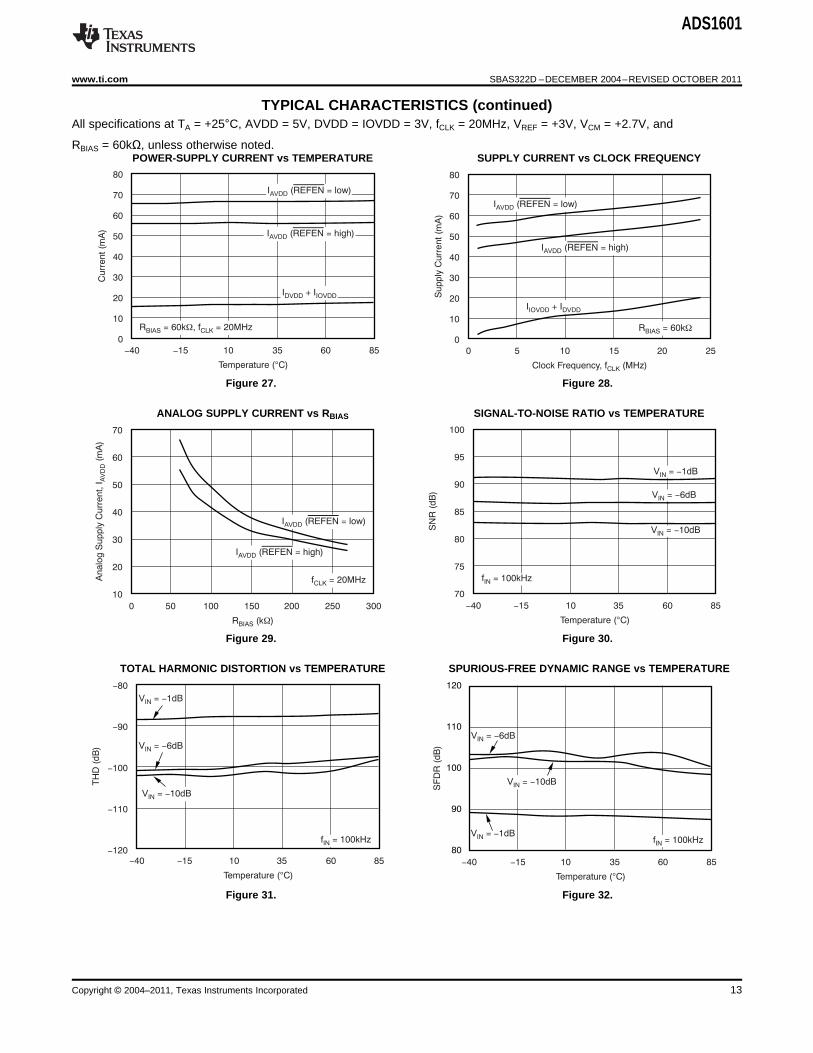
TYPICAL CHARACTERISTICS (continued)All specifications at TA = +25°C, AVDD = 5V, DVDD = IOVDD = 3V, fCLK = 20MHz, VREF = +3V, VCM = +2.7V, and
RBIAS = 60kΩ, unless otherwise noted.POWER-SUPPLY CURRENT vs TEMPERATURE SUPPLY CURRENT vs CLOCK FREQUENCY
Figure 27. Figure 28.
ANALOG SUPPLY CURRENT vs RBIAS SIGNAL-TO-NOISE RATIO vs TEMPERATURE
Figure 29. Figure 30.
TOTAL HARMONIC DISTORTION vs TEMPERATURE SPURIOUS-FREE DYNAMIC RANGE vs TEMPERATURE
Figure 31. Figure 32.
Copyright © 2004–2011, Texas Instruments Incorporated 13

V(V
)R
EF
3.00
2.99
2.98
2.97
2.96
2.95
2.94
2.93
2.92
2.91
2.90
-40 -15 10 35 60 85
Temperature (°C)
0
-20
-40
-60
-80
-100
-120
-140
Am
plit
ude
(d
B)
f =IN1 499kHz
f =IN2 501kHz
IMD = 94dB-
480 485 490 495 500 505 510 515 520
Frequency (kHz)
ADS1601
SBAS322D –DECEMBER 2004–REVISED OCTOBER 2011 www.ti.com
TYPICAL CHARACTERISTICS (continued)All specifications at TA = +25°C, AVDD = 5V, DVDD = IOVDD = 3V, fCLK = 20MHz, VREF = +3V, VCM = +2.7V, and
RBIAS = 60kΩ, unless otherwise noted.VREF vs TEMPERATURE INTERMODULATION RESPONSE
Figure 33. Figure 34.
14 Copyright © 2004–2011, Texas Instruments Incorporated
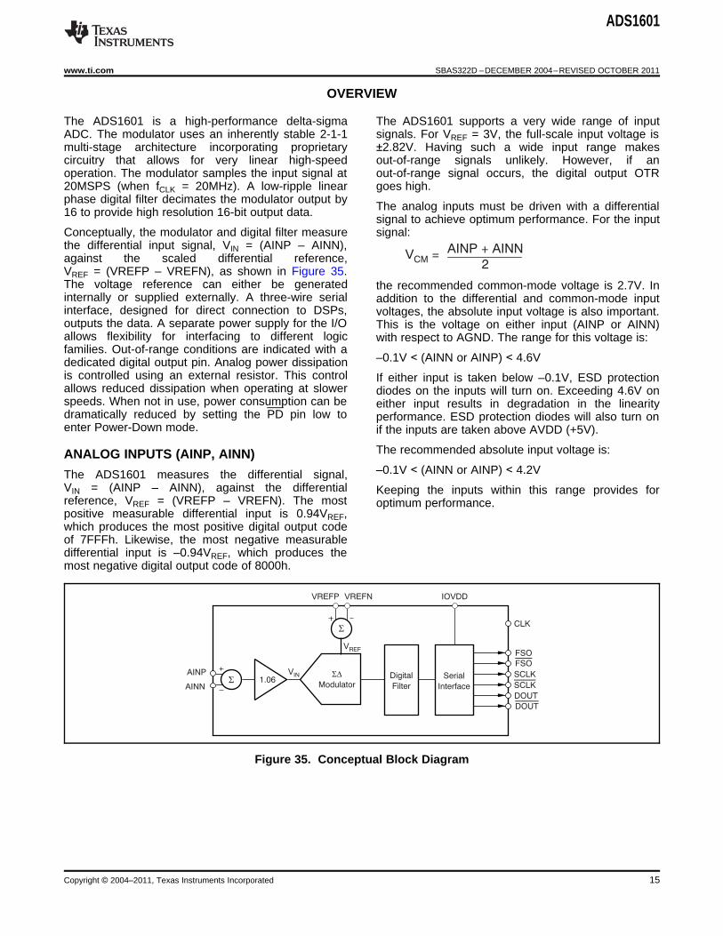
AINP + AINN
2V =CM
SD
ModulatorDigital
Filter
Serial
Interface
S
VIN
VREFN IOVDDVREFP
VREF
SAINP
AINN
FSO
FSO
DOUT
DOUT
SCLK
SCLK
CLK
1.06
ADS1601
www.ti.com SBAS322D –DECEMBER 2004–REVISED OCTOBER 2011
OVERVIEW
The ADS1601 is a high-performance delta-sigma The ADS1601 supports a very wide range of inputADC. The modulator uses an inherently stable 2-1-1 signals. For VREF = 3V, the full-scale input voltage ismulti-stage architecture incorporating proprietary ±2.82V. Having such a wide input range makescircuitry that allows for very linear high-speed out-of-range signals unlikely. However, if anoperation. The modulator samples the input signal at out-of-range signal occurs, the digital output OTR20MSPS (when fCLK = 20MHz). A low-ripple linear goes high.phase digital filter decimates the modulator output by
The analog inputs must be driven with a differential16 to provide high resolution 16-bit output data.signal to achieve optimum performance. For the input
Conceptually, the modulator and digital filter measure signal:the differential input signal, VIN = (AINP – AINN),against the scaled differential reference,VREF = (VREFP – VREFN), as shown in Figure 35.The voltage reference can either be generated the recommended common-mode voltage is 2.7V. Ininternally or supplied externally. A three-wire serial addition to the differential and common-mode inputinterface, designed for direct connection to DSPs, voltages, the absolute input voltage is also important.outputs the data. A separate power supply for the I/O This is the voltage on either input (AINP or AINN)allows flexibility for interfacing to different logic with respect to AGND. The range for this voltage is:families. Out-of-range conditions are indicated with a
–0.1V < (AINN or AINP) < 4.6Vdedicated digital output pin. Analog power dissipationis controlled using an external resistor. This control If either input is taken below –0.1V, ESD protectionallows reduced dissipation when operating at slower diodes on the inputs will turn on. Exceeding 4.6V onspeeds. When not in use, power consumption can be either input results in degradation in the linearitydramatically reduced by setting the PD pin low to performance. ESD protection diodes will also turn onenter Power-Down mode. if the inputs are taken above AVDD (+5V).
The recommended absolute input voltage is:ANALOG INPUTS (AINP, AINN)–0.1V < (AINN or AINP) < 4.2VThe ADS1601 measures the differential signal,
VIN = (AINP – AINN), against the differential Keeping the inputs within this range provides forreference, VREF = (VREFP – VREFN). The most optimum performance.positive measurable differential input is 0.94VREF,which produces the most positive digital output codeof 7FFFh. Likewise, the most negative measurabledifferential input is –0.94VREF, which produces themost negative digital output code of 8000h.
Figure 35. Conceptual Block Diagram
Copyright © 2004–2011, Texas Instruments Incorporated 15

S1
S2
10pF
AINP
ADS1601
8pF
VMID
S1
S2
10pF
AINN
8pF
VMID
AGND
392W
OPA2822
ADS1601
AGND
OPA2822
40pF
VCM
(1)
VCM
(1)
VCM
(1)
100pF
AINP
AINN
100pF(3)
392W
40pF
100pF
(2)
(2)
(2)
(2)
392W
392W
392W
0.01 Fm
0.01 Fm
392W
1 Fm392W 1kW
1kW
1 Fm392W
49.9W
49.9W
-V
IN
2+ V
CM
VIN
2+ V
CM
On
S1
S2
Off
On
Off
t = fSAMPLE CLK1/
ADS1601THS4503
22pF
-VIN
+VIN
100pF
100pF
AINP
AINN
100pF
24.9W
392W
392W 24.9W
392W
392W
22pF
VCM
ADS1601
SBAS322D –DECEMBER 2004–REVISED OCTOBER 2011 www.ti.com
INPUT CIRCUITRY drivers close to the inputs and use good capacitorbypass techniques on their supplies, such as a
The ADS1601 uses switched-capacitor circuitry to smaller high-quality ceramic capacitor in parallel withmeasure the input voltage. Internal capacitors are a larger capacitor. Keep the resistances used in thecharged by the inputs and then discharged internally driver circuits low—thermal noise in the driver circuitswith this cycle repeating at the frequency of CLK. degrades the overall noise performance. When theFigure 36 shows a conceptual diagram of these signal can be ac-coupled to the ADS1601 inputs, acircuits. Switches S2 represent the net effect of the simple RC filter can set the input common-modemodulator circuitry in discharging the sampling voltage. The ADS1601 is a high-speed,capacitors; the actual implementation is different. The high-performance ADC. Special care must be takentiming for switches S1 and S2 is shown in Figure 37. when selecting the test equipment and setup used
with this device. Pay particular attention to the signalsources to ensure they do not limit performance whenmeasuring the ADS1601.
Figure 36. Conceptual Diagram of InternalCircuitry Connected to the Analog Inputs
(1) Recommended VCM = 2.7V.
(2) Optional ac-coupling circuit provides common-mode inputvoltage.
(3) Increase to 390pF when fIN ≤ 100kHz for improved SNR andTHD.
Figure 38. Recommended Driver Circuit Usingthe OPA2822
Figure 37. Timing for the Switches in Figure 36
DRIVING THE INPUTS
The external circuits driving the ADS1601 inputs mustbe able to handle the load presented by the switchingcapacitors within the ADS1601. The input switches S1in Figure 36 are closed for approximately one-half ofthe sampling period, tSAMPLE, allowing only ≉ 24ns forthe internal capacitors to be charged by the inputswhen fCLK = 20MHz.
Figure 38 and Figure 39 show the recommendedcircuits when using single-ended or differential opamps, respectively. The analog inputs must be driven Figure 39. Recommended Driver Circuit Usingdifferentially to achieve optimum performance. The the THS4503 Differential Amplifierexternal capacitors, between the inputs and fromeach input to AGND, improve linearity and should beplaced as close to the pins as possible. Place the
16 Copyright © 2004–2011, Texas Instruments Incorporated

S1
ADS1601
S2
VREFP
50pF300W
S1
VREFN
VREFP
VREFN
10 Fm
0.1 Fm
0.1 Fm
10 Fm 0.1 Fm
10 Fm 0.1 Fm
0.1 Fm
ADS1601
AGND
VREFP
VREFP
VMID
VCAP
VREFN
VREFN
ADS1601
www.ti.com SBAS322D –DECEMBER 2004–REVISED OCTOBER 2011
REFERENCE INPUTS (VREFN, VREFP, VMID) EXTERNAL REFERENCE (REFEN = HIGH)
The ADS1601 can operate from an internal or To use an external reference, set the REFEN pinexternal voltage reference. In either case, the high. This deactivates the internal generators forreference voltage VREF is set by the differential VREFP, VREFN, and VMID, and savesvoltage between VREFN and VREFP: VREF = approximately 25mA of current on the analog supply(VREFP – VREFN). VREFP and VREFN each use (AVDD). The voltages applied to these pins must betwo pins, which should be shorted together. VMID within the values specified in the Electricalequals approximately 2.5V and is used by the Characteristics table. Typically, VREFP = 4V, VMID =modulator. VCAP connects to an internal node and 2.5V, and VREFN = 1V. The external circuitry mustmust also be bypassed with an external capacitor. be capable of providing both a dc and a transient
current. Figure 41 shows a simplified diagram of theinternal circuitry of the reference when the internalINTERNAL REFERENCE (REFEN = LOW)reference is disabled. As with the input circuitry,
To use the internal reference, set the REFEN pin low. switches S1 and S2 open and close as shown by theThis activates the internal circuitry that generates the timing in Figure 37.reference voltages. The internal reference voltagesare applied to the pins. Good bypassing of thereference pins is critical to achieve optimumperformance and is done by placing the bypasscapacitors as close to the pins as possible. Figure 40shows the recommended bypass capacitor values.Use high-quality ceramic capacitors for the smallervalues. Avoid loading the internal reference withexternal circuitry. If the ADS1601 internal reference isto be used by other circuitry, buffer the referencevoltages to prevent directly loading the referencepins. Figure 41. Conceptual Internal Circuitry for the
Reference When REFEN = High
Figure 42 shows the recommended circuitry fordriving these reference inputs. Keep the resistancesused in the buffer circuits low to prevent excessivethermal noise from degrading performance. Layout ofthese circuits is critical; be sure to follow goodhigh-speed layout practices. Place the buffers, andespecially the bypass capacitors, as close to the pinsas possible. VCAP is unaffected by the setting onREFEN and must be bypassed when using theinternal or an external reference.
Figure 40. Reference Bypassing When Using theInternal Reference
Copyright © 2004–2011, Texas Instruments Incorporated 17

10 Fm
0.1 Fm
0.1 Fm
10 Fm 0.1 Fm
10 Fm0.1 Fm
0.1 Fm
VREFP
VREFP
VMID
VCAP
VREFN
VREFN
392W
OPA2822
ADS1601
0.001 Fm
4V
392W
OPA2822
0.001 Fm
1V
392W
OPA2822
0.001 Fm
2.5V
AGND
+0.94V
2 1
REF
-15
-0.94V
2 1
REF
-15
-REF
0.94V2
2 1-
15
15( )
£ -REF
0.94V2
2 1-
15
15( )
ADS1601
SBAS322D –DECEMBER 2004–REVISED OCTOBER 2011 www.ti.com
Table 1. Maximum Allowable Clock Source Jitterfor Different Input Signal Frequencies and
Amplitude
INPUT SIGNAL
MAXIMUM MAXIMUM MAXIMUM ALLOWABLEFREQUENCY AMPLITUDE CLOCK SOURCE JITTER
500kHz –0.5dB 6ps
500kHz –20dB 60ps
100kHz –0.5dB 30ps
100kHz –20dB 300ps
DATA FORMAT
The 16-bit output data are in binary two’scomplement format as shown in Table 2. When theinput is positive out-of-range, exceeding the positivefull-scale value of +0.94VREF, the output clips to all7FFFh and the OTR output goes high.
Likewise, when the input is negative out-of-range bygoing below the negative full-scale valueof –0.94VREF, the output clips to 8000h and the OTRoutput goes high. The OTR remains high while theinput signal is out-of-range.Figure 42. Recommended Buffer Circuit When
Using an External ReferenceTable 2. Output Code versus Input Signal
INPUT SIGNAL (INP – IDEAL OUTPUTCLOCK INPUT (CLK) INN) CODE(1) OTR
≥ +0.94VREF (> 0dB) 7FFFh 1The ADS1601 requires an external clock signal to be–0.94VREF (0dB) 7FFFh 0applied to the CLK input pin. The sampling of the
modulator is controlled by this clock signal. As with001h 0any high-speed data converter, a high quality clock is
essential for optimum performance. Crystal clock0 0000h 0oscillators are the recommended CLK source; other
sources, such as frequency synthesizers, are usuallyFFFFh 0inadequate. Make sure to avoid excess ringing on the
CLK input; keeping the trace as short as possiblehelps.
8000h 0Measuring high-frequency, large amplitude signalsrequires tight control of clock jitter. The uncertaintyduring sampling of the input from clock jitter limits the 8000h 1maximum achievable SNR. This effect becomes morepronounced with higher frequency and larger (1) Excludes effects of noise, INL, offset and gain errors.magnitude inputs. Fortunately, the ADS1601oversampling topology reduces clock jitter sensitivity OUT-OF-RANGE INDICATION (OTR)over that of Nyquist rate converters such as pipeline
If the output code exceeds the positive or negativeand successive approximation converters by a factorfull-scale, the out-of-range digital output OTR will goof √16.high on the falling edge of SCLK. When the output
In order to not limit the ADS1601 SNR performance, code returns within the full-scale range, OTR returnskeep the jitter on the clock source below the values low on the falling edge of SCLK.shown in Table 1. When measuring lower frequencyand lower amplitude inputs, more CLK jitter can betolerated. In determining the allowable clock sourcejitter, select the worst-case input (highest frequency,largest amplitude) that will be seen in the application.
18 Copyright © 2004–2011, Texas Instruments Incorporated

1.2
1.0
0.8
0.6
0.4
0.2
0
-0.2
0 10 20 30 40
Time (Conversion Cycles)
Ste
p R
esponse
50
20
0
-20
-40
-60
-80
-100
-120
-140
0 1 2 3 54 6 7 8 9
Frequency (MHz)
Magnitude (
dB
)
10
f =CLK 20MHz
SYNC
ADS16011
CLK
FSO
DOUT
FSO1
DOUT1
SYNC
CLK
SYNC
ADS16012
CLK
FSO
DOUT
CLK
SYNC
FSO1
FSO2
tSTL
FSO2
DOUT2
ADS1601
www.ti.com SBAS322D –DECEMBER 2004–REVISED OCTOBER 2011
DATA RETRIEVAL STEP RESPONSE
Data retrieval is controlled through a simple serial Figure 44 plots the normalized step response for aninterface. The interface operates in a master fashion input applied at t = 0. The x-axis units of time areby outputting both a frame sync indicator (FSO) and a conversions cycles. It takes 51 cycles to fully settle;serial clock (SCLK). Complementary outputs are for fCLK = 20MHz, this corresponds to 40.8μs.provided for the frame sync output (FSO), serial clock(SCLK), and data output (DOUT). When not needed,leave the complementary outputs unconnected.
INITIALIZING THE ADS1601
After the power supplies have stabilized, you mustinitialize the ADS1601 by issuing a SYNC pulse asshown in Figure 1. This operation needs only to bedone once after power-up and does not need to beperformed when exiting the Power-Down mode. Notethat the ADS1601 silicon was revised in June 2006.The digital interface timing specifications weremodified slightly from the previous revision. This datasheet reflects behavior of the latest revision. Contactthe factory for more information on the previousrevision.
Figure 44. Step ResponseSYNCHRONIZING MULTIPLE ADS1601s
The SYNC input can be used to synchronize multiple FREQUENCY RESPONSEADS1601s to provide simultaneous sampling. Alldevices to be synchronized must use a common CLK The linear phase FIR digital filter sets the overallinput. With the CLK inputs running, pulse SYNC on frequency response. Figure 45 shows the frequencythe falling edge of CLK, as shown in Figure 43. response from dc to 10MHz for fCLK = 20MHz. TheAfterwards, the converters will be converting frequency response of the ADS1601 filter scalessynchronously with the FSO outputs updating directly with CLK frequency. For example, if the CLKsimultaneously. After synchronization, FSO is held frequency is decreased by half (to 10MHz), thelow until the digital filter has fully settled. values on the X-axis in Figure 45 would need to be
scaled by half, with the span becoming dc to 5MHz.Figure 46 shows the passband ripple from dc to600kHz (fCLK = 20MHz). Figure 47 shows a closerview of the passband transition by plotting theresponse from 400kHz to 650kHz (fCLK = 20MHz).
Figure 45. Frequency Response
Figure 43. Synchronizing Multiple Converters
Copyright © 2004–2011, Texas Instruments Incorporated 19
0.001
0.0008
0.0006
0.0004
0.0002
0
-0.0002
-0.0004
-0.0006
-0.0008
-0.001
0 100 200 300
Frequency (kHz)
400 500
Mag
nitud
e (
dB
)
600
f = 20CLK MHz
20
0
-20
-40
-60
-80
-100
-120
-140
0 10 20 30 40 50
Frequency (MHz)
Magnitude (
dB
)
60
f = 20CLK MHz
0.5
0
-0.5
-1.0
-1.5
-2.0
-2.5
-3.0
-3.5
400 450 500 550 600
Frequency (kHz)
Magnitude (
dB
)
650
f = 20CLK MHz
RBIAS
RBIAS
AGND
ADS1601
ADS1601
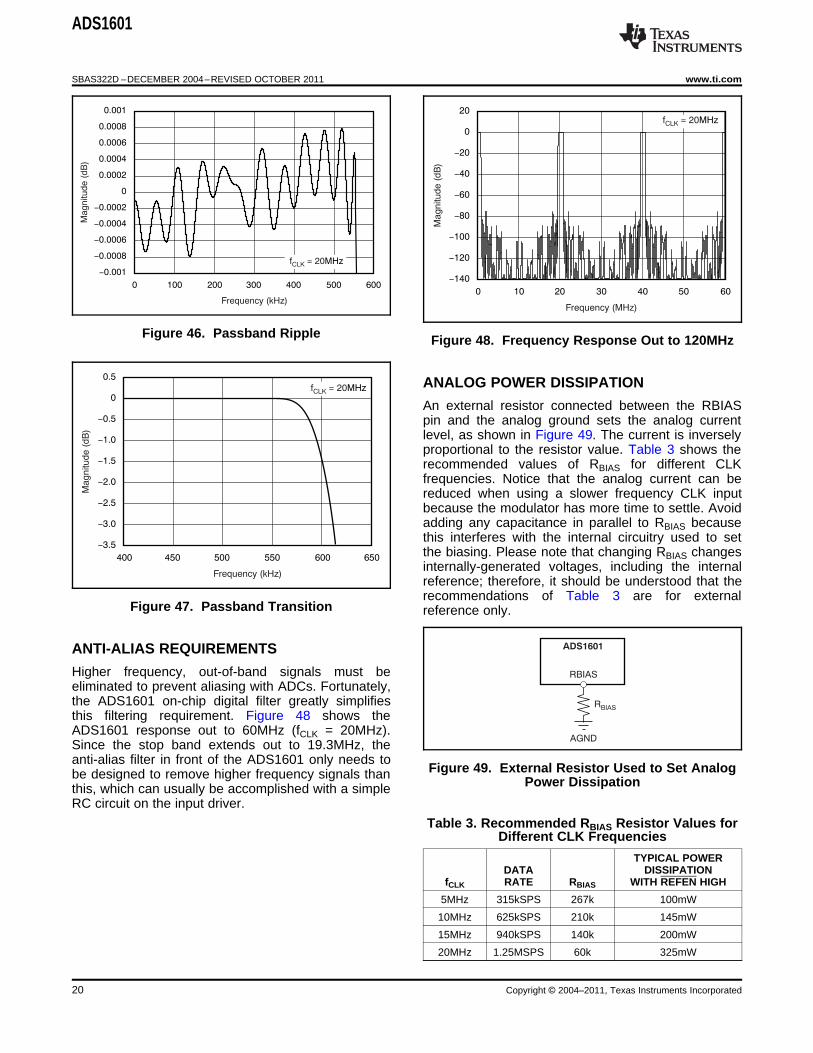
SBAS322D –DECEMBER 2004–REVISED OCTOBER 2011 www.ti.com
Figure 46. Passband Ripple Figure 48. Frequency Response Out to 120MHz
ANALOG POWER DISSIPATION
An external resistor connected between the RBIASpin and the analog ground sets the analog currentlevel, as shown in Figure 49. The current is inverselyproportional to the resistor value. Table 3 shows therecommended values of RBIAS for different CLKfrequencies. Notice that the analog current can bereduced when using a slower frequency CLK inputbecause the modulator has more time to settle. Avoidadding any capacitance in parallel to RBIAS becausethis interferes with the internal circuitry used to setthe biasing. Please note that changing RBIAS changesinternally-generated voltages, including the internalreference; therefore, it should be understood that therecommendations of Table 3 are for external
Figure 47. Passband Transition reference only.
ANTI-ALIAS REQUIREMENTS
Higher frequency, out-of-band signals must beeliminated to prevent aliasing with ADCs. Fortunately,the ADS1601 on-chip digital filter greatly simplifiesthis filtering requirement. Figure 48 shows theADS1601 response out to 60MHz (fCLK = 20MHz).Since the stop band extends out to 19.3MHz, theanti-alias filter in front of the ADS1601 only needs to
Figure 49. External Resistor Used to Set Analogbe designed to remove higher frequency signals than Power Dissipationthis, which can usually be accomplished with a simpleRC circuit on the input driver.
Table 3. Recommended RBIAS Resistor Values forDifferent CLK Frequencies
TYPICAL POWERDATA DISSIPATION
fCLK RATE RBIAS WITH REFEN HIGH
5MHz 315kSPS 267k 100mW
10MHz 625kSPS 210k 145mW
15MHz 940kSPS 140k 200mW
20MHz 1.25MSPS 60k 325mW
20 Copyright © 2004–2011, Texas Instruments Incorporated
CP
CP
CP
CP
CP CP
CPCP
1 36DGND
2
3
9
10
11
12
18
42 41 55 38 37 34 33
19 22 23
AVDD
AVDD
AGND
AGND
CP
6
7 AVDD
AGND
AGND
AVDD
47 Fm
47 Fm
47 Fm 4.7 Fm 1 Fm 0.1 Fm
0.1 Fm
0.1 Fm
1 Fm
1 Fm
4.7 Fm
4.7 FmD
VD
D
AV
DD
AG
ND
AG
ND
DG
ND
IOV
DD
DV
DD
DG
ND
DG
ND
15
10kW
RP
ULLU
P
DG
ND
DV
DD
ADS1601
If using separate analog and
digital ground planes, connect
together on the ADS1601 PCB.
DGND
NOTE: C =P 1 Fm úú m0.1 F
AGND
AVDD
IOVDD
DVDD
ADS1601
www.ti.com SBAS322D –DECEMBER 2004–REVISED OCTOBER 2011
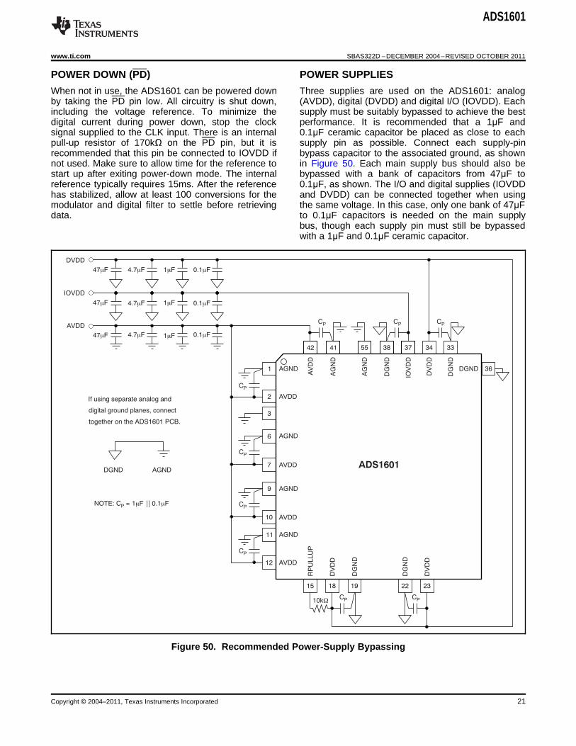
POWER DOWN (PD) POWER SUPPLIES
When not in use, the ADS1601 can be powered down Three supplies are used on the ADS1601: analogby taking the PD pin low. All circuitry is shut down, (AVDD), digital (DVDD) and digital I/O (IOVDD). Eachincluding the voltage reference. To minimize the supply must be suitably bypassed to achieve the bestdigital current during power down, stop the clock performance. It is recommended that a 1μF andsignal supplied to the CLK input. There is an internal 0.1μF ceramic capacitor be placed as close to eachpull-up resistor of 170kΩ on the PD pin, but it is supply pin as possible. Connect each supply-pinrecommended that this pin be connected to IOVDD if bypass capacitor to the associated ground, as shownnot used. Make sure to allow time for the reference to in Figure 50. Each main supply bus should also bestart up after exiting power-down mode. The internal bypassed with a bank of capacitors from 47μF toreference typically requires 15ms. After the reference 0.1μF, as shown. The I/O and digital supplies (IOVDDhas stabilized, allow at least 100 conversions for the and DVDD) can be connected together when usingmodulator and digital filter to settle before retrieving the same voltage. In this case, only one bank of 47μFdata. to 0.1μF capacitors is needed on the main supply
bus, though each supply pin must still be bypassedwith a 1μF and 0.1μF ceramic capacitor.
Figure 50. Recommended Power-Supply Bypassing
Copyright © 2004–2011, Texas Instruments Incorporated 21

FSO
ADS1601
SCLK
DOUT
SYNC
FSR
TMS320
CLKR
DR
FSX
ADS1601
SBAS322D –DECEMBER 2004–REVISED OCTOBER 2011 www.ti.com
LAYOUT ISSUES AND COMPONENT The McBSP provides a host of functions including:SELECTION • Full-duplex communication
• Double-buffered data registersThe ADS1601 is a very high-speed, high-resolutiondata converter. In order to achieve maximum • Independent framing and clocking for receptionperformance, the user must give very careful and transmission of dataconsideration to both the layout of the printed circuit
The sequence begins with a one-time synchronizationboard (PCB) in addition to the routing of the traces.of the serial port by the microprocessor. TheCapacitors that are critical to achieve the bestADS1601 recognizes the SYNC signal if it is high forperformance from the device should be placed asat least one CLK period. Transfers are initiated by theclose to the pins of the device as possible. TheseADS1601 after the SYNC signal is de-asserted by theinclude capacitors related to the analog inputs, themicroprocessor.reference, and the power supplies.The FSO signal from the ADS1601 indicates thatFor critical capacitors, it is recommended that Class IIdata is available to be read, and is connected to thedielectrics such as Z5U be avoided. These dielectricsframe sync receive (FSR) pin of the DSP. The clockhave a narrow operating temperature, a largereceiver (CLKR) is derived directly from the ADS1601tolerance on the capacitance, and lose up to 20% ofserial clock output to ensure continuedthe rated capacitance over 10,000 hours. Rather,synchronization of data with the clock.select capacitors with a Class I dielectric. C0G (also
known as NP0), for example, has a tight toleranceless than ±30ppm/°C and is very stable over time.Should Class II capacitors be chosen because of thesize constraints, select an X7R or X5R dielectric tominimize the variations of the capacitor’s criticalcharacteristics.
The resistors used in the circuits to drive the inputand reference should be kept as low as possible toprevent excess thermal noise from degrading thesystem performance.
The digital outputs from the device should always bebuffered. This will have a number of benefits: it Figure 51. ADS1601—TMS320 Interfacereduces the loading of the internal digital buffers, Connectionwhich decreases noise generated within the device,and it also reduces device power consumption.
An evaluation module (EVM) is available from TexasInstruments. The module consists of the ADS1601APPLICATIONS INFORMATIONand supporting circuits, allowing users to quicklyassess the performance and characteristics of theInterfacing the ADS1601 to the TMS320 DSPADS1601. The EVM easily connects to variousfamily.microcontrollers and DSP systems. For more details,
Since the ADS1601 communicates with the host via a or to download a copy of the ADS1601EVM User’sserial interface, the most suitable method to connect Guide, visit the Texas Instruments web site atto any of the TMS320 DSPs is via the multi-channel www.ti.com.buffered serial port (McBSP). A typical connection tothe TMS320 DSP is shown in Figure 51.
22 Copyright © 2004–2011, Texas Instruments Incorporated

ADS1601
www.ti.com SBAS322D –DECEMBER 2004–REVISED OCTOBER 2011
REVISION HISTORY
NOTE: Page numbers for previous revisions may differ from page numbers in the current version.
Changes from Revision C (September 2010) to Revision D Page
• Added footnote 1 to Electrical Characteristics table ............................................................................................................. 4
Changes from Revision B (September 2008) to Revision C Page
• Changed the Timing Diagrams section ................................................................................................................................. 8
• Added note to Initializing the ADS1601 section .................................................................................................................. 19
• Updated Figure 43 .............................................................................................................................................................. 19
Copyright © 2004–2011, Texas Instruments Incorporated 23

PACKAGE OPTION ADDENDUM
www.ti.com 10-Jun-2014
Addendum-Page 1
PACKAGING INFORMATION
Orderable Device Status(1)
Package Type PackageDrawing
Pins PackageQty
Eco Plan(2)
Lead/Ball Finish(6)
MSL Peak Temp(3)
Op Temp (°C) Device Marking(4/5)
Samples
ADS1601IPFBR ACTIVE TQFP PFB 48 1000 Green (RoHS& no Sb/Br)
CU NIPDAU Level-2-260C-1 YEAR -40 to 85 ADS1601I
ADS1601IPFBT ACTIVE TQFP PFB 48 250 Green (RoHS& no Sb/Br)
CU NIPDAU Level-2-260C-1 YEAR -40 to 85 ADS1601I
ADS1601IPFBTG4 ACTIVE TQFP PFB 48 250 Green (RoHS& no Sb/Br)
CU NIPDAU Level-2-260C-1 YEAR -40 to 85 ADS1601I
(1) The marketing status values are defined as follows:ACTIVE: Product device recommended for new designs.LIFEBUY: TI has announced that the device will be discontinued, and a lifetime-buy period is in effect.NRND: Not recommended for new designs. Device is in production to support existing customers, but TI does not recommend using this part in a new design.PREVIEW: Device has been announced but is not in production. Samples may or may not be available.OBSOLETE: TI has discontinued the production of the device.
(2) Eco Plan - The planned eco-friendly classification: Pb-Free (RoHS), Pb-Free (RoHS Exempt), or Green (RoHS & no Sb/Br) - please check http://www.ti.com/productcontent for the latest availabilityinformation and additional product content details.TBD: The Pb-Free/Green conversion plan has not been defined.Pb-Free (RoHS): TI's terms "Lead-Free" or "Pb-Free" mean semiconductor products that are compatible with the current RoHS requirements for all 6 substances, including the requirement thatlead not exceed 0.1% by weight in homogeneous materials. Where designed to be soldered at high temperatures, TI Pb-Free products are suitable for use in specified lead-free processes.Pb-Free (RoHS Exempt): This component has a RoHS exemption for either 1) lead-based flip-chip solder bumps used between the die and package, or 2) lead-based die adhesive used betweenthe die and leadframe. The component is otherwise considered Pb-Free (RoHS compatible) as defined above.Green (RoHS & no Sb/Br): TI defines "Green" to mean Pb-Free (RoHS compatible), and free of Bromine (Br) and Antimony (Sb) based flame retardants (Br or Sb do not exceed 0.1% by weightin homogeneous material)
(3) MSL, Peak Temp. - The Moisture Sensitivity Level rating according to the JEDEC industry standard classifications, and peak solder temperature.
(4) There may be additional marking, which relates to the logo, the lot trace code information, or the environmental category on the device.
(5) Multiple Device Markings will be inside parentheses. Only one Device Marking contained in parentheses and separated by a "~" will appear on a device. If a line is indented then it is a continuationof the previous line and the two combined represent the entire Device Marking for that device.
(6) Lead/Ball Finish - Orderable Devices may have multiple material finish options. Finish options are separated by a vertical ruled line. Lead/Ball Finish values may wrap to two lines if the finishvalue exceeds the maximum column width.
Important Information and Disclaimer:The information provided on this page represents TI's knowledge and belief as of the date that it is provided. TI bases its knowledge and belief on informationprovided by third parties, and makes no representation or warranty as to the accuracy of such information. Efforts are underway to better integrate information from third parties. TI has taken and

PACKAGE OPTION ADDENDUM
www.ti.com 10-Jun-2014
Addendum-Page 2
continues to take reasonable steps to provide representative and accurate information but may not have conducted destructive testing or chemical analysis on incoming materials and chemicals.TI and TI suppliers consider certain information to be proprietary, and thus CAS numbers and other limited information may not be available for release.
In no event shall TI's liability arising out of such information exceed the total purchase price of the TI part(s) at issue in this document sold by TI to Customer on an annual basis.

TAPE AND REEL INFORMATION
*All dimensions are nominal
Device PackageType
PackageDrawing
Pins SPQ ReelDiameter
(mm)
ReelWidth
W1 (mm)
A0(mm)
B0(mm)
K0(mm)
P1(mm)
W(mm)
Pin1Quadrant
ADS1601IPFBR TQFP PFB 48 1000 330.0 16.4 9.6 9.6 1.5 12.0 16.0 Q2
ADS1601IPFBT TQFP PFB 48 250 180.0 16.4 9.6 9.6 1.5 12.0 16.0 Q2
PACKAGE MATERIALS INFORMATION
www.ti.com 7-Feb-2015
Pack Materials-Page 1

*All dimensions are nominal
Device Package Type Package Drawing Pins SPQ Length (mm) Width (mm) Height (mm)
ADS1601IPFBR TQFP PFB 48 1000 367.0 367.0 38.0
ADS1601IPFBT TQFP PFB 48 250 213.0 191.0 55.0
PACKAGE MATERIALS INFORMATION
www.ti.com 7-Feb-2015
Pack Materials-Page 2

MECHANICAL DATA
MTQF019A – JANUARY 1995 – REVISED JANUARY 1998
POST OFFICE BOX 655303 • DALLAS, TEXAS 75265
PFB (S-PQFP-G48) PLASTIC QUAD FLATPACK
4073176/B 10/96
Gage Plane
0,13 NOM
0,25
0,450,75
Seating Plane
0,05 MIN
0,170,27
24
25
13
12
SQ
36
37
7,206,80
48
1
5,50 TYP
SQ8,809,20
1,050,95
1,20 MAX0,08
0,50 M0,08
0°–7°
NOTES: A. All linear dimensions are in millimeters.B. This drawing is subject to change without notice.C. Falls within JEDEC MS-026


IMPORTANT NOTICE
Texas Instruments Incorporated and its subsidiaries (TI) reserve the right to make corrections, enhancements, improvements and otherchanges to its semiconductor products and services per JESD46, latest issue, and to discontinue any product or service per JESD48, latestissue. Buyers should obtain the latest relevant information before placing orders and should verify that such information is current andcomplete. All semiconductor products (also referred to herein as “components”) are sold subject to TI’s terms and conditions of salesupplied at the time of order acknowledgment.TI warrants performance of its components to the specifications applicable at the time of sale, in accordance with the warranty in TI’s termsand conditions of sale of semiconductor products. Testing and other quality control techniques are used to the extent TI deems necessaryto support this warranty. Except where mandated by applicable law, testing of all parameters of each component is not necessarilyperformed.TI assumes no liability for applications assistance or the design of Buyers’ products. Buyers are responsible for their products andapplications using TI components. To minimize the risks associated with Buyers’ products and applications, Buyers should provideadequate design and operating safeguards.TI does not warrant or represent that any license, either express or implied, is granted under any patent right, copyright, mask work right, orother intellectual property right relating to any combination, machine, or process in which TI components or services are used. Informationpublished by TI regarding third-party products or services does not constitute a license to use such products or services or a warranty orendorsement thereof. Use of such information may require a license from a third party under the patents or other intellectual property of thethird party, or a license from TI under the patents or other intellectual property of TI.Reproduction of significant portions of TI information in TI data books or data sheets is permissible only if reproduction is without alterationand is accompanied by all associated warranties, conditions, limitations, and notices. TI is not responsible or liable for such altereddocumentation. Information of third parties may be subject to additional restrictions.Resale of TI components or services with statements different from or beyond the parameters stated by TI for that component or servicevoids all express and any implied warranties for the associated TI component or service and is an unfair and deceptive business practice.TI is not responsible or liable for any such statements.Buyer acknowledges and agrees that it is solely responsible for compliance with all legal, regulatory and safety-related requirementsconcerning its products, and any use of TI components in its applications, notwithstanding any applications-related information or supportthat may be provided by TI. Buyer represents and agrees that it has all the necessary expertise to create and implement safeguards whichanticipate dangerous consequences of failures, monitor failures and their consequences, lessen the likelihood of failures that might causeharm and take appropriate remedial actions. Buyer will fully indemnify TI and its representatives against any damages arising out of the useof any TI components in safety-critical applications.In some cases, TI components may be promoted specifically to facilitate safety-related applications. With such components, TI’s goal is tohelp enable customers to design and create their own end-product solutions that meet applicable functional safety standards andrequirements. Nonetheless, such components are subject to these terms.No TI components are authorized for use in FDA Class III (or similar life-critical medical equipment) unless authorized officers of the partieshave executed a special agreement specifically governing such use.Only those TI components which TI has specifically designated as military grade or “enhanced plastic” are designed and intended for use inmilitary/aerospace applications or environments. Buyer acknowledges and agrees that any military or aerospace use of TI componentswhich have not been so designated is solely at the Buyer's risk, and that Buyer is solely responsible for compliance with all legal andregulatory requirements in connection with such use.TI has specifically designated certain components as meeting ISO/TS16949 requirements, mainly for automotive use. In any case of use ofnon-designated products, TI will not be responsible for any failure to meet ISO/TS16949.
Products ApplicationsAudio www.ti.com/audio Automotive and Transportation www.ti.com/automotiveAmplifiers amplifier.ti.com Communications and Telecom www.ti.com/communicationsData Converters dataconverter.ti.com Computers and Peripherals www.ti.com/computersDLP® Products www.dlp.com Consumer Electronics www.ti.com/consumer-appsDSP dsp.ti.com Energy and Lighting www.ti.com/energyClocks and Timers www.ti.com/clocks Industrial www.ti.com/industrialInterface interface.ti.com Medical www.ti.com/medicalLogic logic.ti.com Security www.ti.com/securityPower Mgmt power.ti.com Space, Avionics and Defense www.ti.com/space-avionics-defenseMicrocontrollers microcontroller.ti.com Video and Imaging www.ti.com/videoRFID www.ti-rfid.comOMAP Applications Processors www.ti.com/omap TI E2E Community e2e.ti.comWireless Connectivity www.ti.com/wirelessconnectivity
Mailing Address: Texas Instruments, Post Office Box 655303, Dallas, Texas 75265Copyright © 2015, Texas Instruments Incorporated