15.1 introduction-definitons and amplifier …...1 power amplifiers 15.1 introduction-definitons and...
TRANSCRIPT
1
POWER AMPLIFIERS
15.1 INTRODUCTION-DEFINITONS AND AMPLIFIER TYPES
An Amplifier receives a signal from some pickup transducer or other input source and provides a
larger version of the signal to some output device or to another amplifier stage. An input transducer
signal is generally small (a few millivolts from a cassette or CD input or a few microvolts from an
antenna) and needs to be amplified sufficiently to operate an output device (speaker or other power-
handling device). In small signal amplifiers, the main factors are usually amplification linearity and
magnitude of gain , since signal voltage and current are small in a small-signal amplifier, the amount
of power-handling capacity and power efficiency are of little concern. A voltage amplifier provides
voltage amplification primarily to increase the voltage of the input signal. Large-signal or power
amplifiers, on the other hand, primarily provide sufficient power to an output load to drive a speaker or
other power device, typically a few watts to tens of watts. In the present chapter, we concentrate on
those amplifier circuits used to handle large-voltage signals at moderate to high current levels. The
main features of a large-signal amplifier are the circuit's power efficiency, the maximum amount of
power that the circuit is capable of handling, and the impedance matching to the output device.
One method used to categorize amplifiers is by class. Basically, amplifier classes represent the
amount the output signal varies over one cycle of operation for a full cycle of input signal. A brief
description of amplifier classes is provided next.
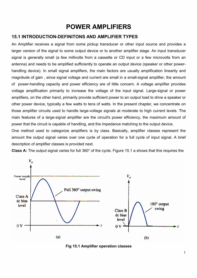
Class A: The output signal varies for full 360° of the cycle. Figure 15.1 a shows that this requires the
Fig 15.1 Amplifier operation classes

2
Q-point to be biased at a level so that at least half the signal swing of the output may vary up and
down without going to a high-enough voltage to be limited by the supply voltage level or too low to
approach the lower supply level, or 0 V in this description
Class B: A class B circuit provides an output signal varying over one-half '.-: input signal cycle, or for
180° of signal, as shown in Fig. 15.1 b. The dc bias point for class B is therefore at 0 V, with the
output then varying from this bias point for a half-cycle. Obviously, the output is not a faithful
reproduction of the input if only one half-cycle is present. Two class B operations-one to provide
output on the positive output half-cycle and another to provide operation on the negative-output half-
cycle are necessary. The combined half-cycles then provide an output for a full 360° of operation.
This type of connection is referred to as push-pull operation, which is discussed later in this chapter.
Note that class B operation by itself creates a very distorted output signal since reproduction of the
input takes place for only 180° of the output signal swing.
Class AB: An amplifier may be biased at a dc level above the zero base current level of class B and
above one-half the supply voltage level of class A; this bias condition is class AB. Class AB operation
still requires a push-pull connection to achieve a full output cycle, but the dc bias level is usually
closer to the zero base current level for better power efficiency, as described shortly. For class AB
operation, the output signal swing occurs between 1800 and 3600 and is neither class A nor class B
operation.
Class C: The output of a class C amplifier is biased for operation at Iess than 180 of the cycle and
will operate only with a tuned (resonant) circuit, which provides a full cycle of operation for the tuned
or resonant frequency. This operating class is therefore used in special areas of tuned circuits, such
as radio or communication.
Class D: This operating class is a form of amplifier operation using pulse (digital) signals, which are
on for a short interval and off for a longer interval. Using digital techniques makes it possible to obtain
a signal that varies over the full cycle (using sample-and-hold circuitry) to recreate the output from
many pieces of input signal. The major advantage of class D operation is that the amplifier is on
(using power) only for short intervals and the overall efficiency can practically be very high, as
described next.

3
Amplifier Efficiency
The power efficiency of an amplifier, defined as the ratio of power output to power input, improves
(gets higher) going from class A to class D. In general terms, we see that a class A amplifier, with dc
bias at one-half the supply voltage level, uses a good amount of power to maintain bias, even with no
input signal applied. This results in very poor efficiency, especially with small input signals, when very
little ac power is delivered to the load, In fact, the maximum efficiency of a class A circuit, occurring
for the largest output voltage and current swing, is only 25% with a direct or series-fed load
connection and 50% with a transformer connection to the load. Class B operation, with no dc bias
power for no input signal, can be shown to provide a maximum efficiency that reaches 78.5%. Class
D operation can achieve power efficiency over 90% and provides the most efficient operation of all
the operating classes. Since class AB falls between class A and class B in bias, it also falls between
their efficiency ratings-between 25% (or 50%) and 78.5%. Table 15.1 summarizes the operation of
the various amplifier classes.
This table provides a relative comparison of the output cycle operation and power efficiency for the
various class types. In class B operation, a push-pull connection is obtained using either a
transformer coupling or by using complementary (or quasi-complementary) operation with npn and
pnp transistors to provide operation on opposite polarity cycles. While transformer operation can
provide opposite cycle signals, the transformer itself is quite large in many application. A transformer
less circuit using complementary transistors provides the same operation in a much smaller package.
Circuits and examples are provided later in this chapter.
15.2 SERIES-FED CLASS A AMPLIFIER
This simple fixed-bias circuit connection shown in Fig. 15.2 can be used to discuss the main features
of a class A series-fed amplifier. The only differences between this circuit and the small-signal version
considered previously is that the signals handled by the large-signal circuit are in the range of volts
and the transistor used is a power transistor that is capable of operating in the range of a few to tens
of watts. As will be shown in this section, this circuit is not the best to use as a large-signal amplifier
because of its poor power efficiency. The beta of a power transistor is generally less than 100, the
overall amplifier circuit using power transistors that are capable of handling large power or current
while not providing much voltage gain.

4
Fig 15.2 Series-fed class A large-signal amplifier
DC Bias Operation
The dc bias set by VCC and RB fixes the dc base-bias current at
With the collector current then being
With the collector-emitter voltage then
To appreciate the importance of the dc bias on the operation of the power amplifier, consider the
collector characteristic shown in Fig. 15.3. An ac load line is drawn using the values of VCC and RC..
The intersection of the dc bias value of IB with the dc load line then determines the operating point (Q-
point) for the circuit. The quiescent point values are those calculated using Eqs. (15.1) through (15.3),
If the dc bias collector current is set at one-half the possible signal swing (between 0 and VCC/RC ),
the largest collector current swing will be possible. Additionally, if the quiescent collector-emitter
voltage is set at one-half the supply voltage, the largest voltage swing will be possible. With the Q-
point set at this optimum bias point, the power considerations for the circuit of Fig. 15.2 are
determined as described below.

5
Fig 15.3Transistor characteristic showing load line and Q-point
AC Operation
When an input ac signal is applied to the amplifier of Fig. 15.2, the output will vary from its dc bias
operating voltage and current. A small input signal, as shown in Fig. 15.4, will cause the base current
to vary above and below the dc bias point, which will then cause the collector current (output) to vary
from the dc bias point set as well as the collector-emitter voltage to vary around its dc bias value.
Fig 15.4 Amplifier input and output signal variation
As the input signal is made larger, the output will vary further around the established dc bias point
until either the current or the voltage reaches a limiting condition. For the current this limiting condition

6
is either zero current at the low end or VCC/RC at the high end of its swing. For the collector-emitter
voltage, the limit is either 0 V or the supply voltage, VCC
Power Consideration
The power into an amplifier is provided by the supply. With no input signal, the dc current drawn is the
collector bias current, ICQ. The power then drawn from the supply is
Even with an ac signal applied, the average current drawn from the supply remains the same, so that
Eq. (15.4) represents the input power supplied to the class A series-fed amplifier
OUTPUT POWER
The output voltage and current varying around the bias point provide ac power to the load. This ac
power is delivered to the load, Rc, in the circuit of Fig. 15.2. The ac signal, Vi, causes the base
current to vary around the dc bias current and the collector current around its quiescent level, ICQ. As
shown in Fig. 15.4, the ac input signal result in ac current and ac voltage signals. The larger the input
signal, the larger the output swing, up to the maximum set by the circuit. The ac power delivered to
the load ( RC ) can be expressed in a number of ways.
Using rms signals: The ac power delivered to the load (Rc) may be expressed using:
Using peak signals: The ac power delivered to the load may be expressed using

7
Using peak-to-peak signals: The ac power delivered to the load may be expressed using
Efficiency
The efficiency of an amplifier represents the amount of ac power delivered (transferred) from the dc
source. The efficiency of the amplifier is calculated using
MAXIMUM EFFICIENCY
For the class A series-fed amplifier, the maximum efficiency can be determined using the maximum
voltage and current swings. For the voltage swing it is
For the current swing it is
Using the maximum voltage swing in Eq.(15.7a) yields

8
The maximum power input can be calculated using the dc bias current set to one-half the maximum
value:
We can then use Eq. (15.8) to calculate the maximum efficiency:
The maximum efficiency of a class A series-fed amplifier is thus seen to be 25%. Since this maximum
efficiency will occur only for ideal conditions of both voltage swing and current swing, most series-fed
circuits will provide efficiencies of much less than 25%.
EXAMPLE 15.1
Calculate the input power, output power, and efficiency of the amplifier circuit in Fig. 15.5 for an input
voltage that results in a base current of 10 mA peak.
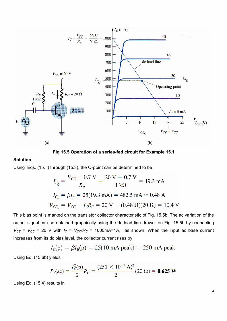
9
Fig 15.5 Operation of a series-fed circuit for Example 15.1
Solution
Using Eqs. (15. I) through (15.3), the Q-point can be determined to be
This bias point is marked on the transistor collector characteristic of Fig. 15.5b. The ac variation of the
output signal can be obtained graphically using the dc load line drawn on Fig. 15.5b by connecting
VCE = VCC = 20 V with IC = VCC/RC = 1000mA=1A, as shown. When the input ac base current
increases from its dc bias level, the collector current rises by
Using Eq. (15.6b) yields
Using Eq. (15.4) results in

10
The amplifier's power efficiency can then be calculated using Eq. (15.8):
15.3 TRANFORMER-COUPLED CLASS A AMPLIFIER
A form of class A amplifier having maximum efficiency of 50% uses a transformer to couple the output
signal to the load as shown in Fig. 15.6. This is a simple circuit:: form to use in presenting a few basic
concepts. More practical circuit versions are covered later. Since the circuit uses a transformer to
step voltage or current, a review of voltage and current step-up and step-down is presented next.
Fig 15.6 Transformer-coupled audio power amplifier
Transformer Action
A transformer can increase or decrease voltage or current levels according to the turns ratio, as
explained below. In addition, the impedance connected to one side of a transformer can be made to
appear either larger or smaller (step up or step down) at the other side of the transformer, depending
on the square of the transformer winding turns ratio. The following discussion assumes ideal (100%)
power transfer from primary to secondary, that is, no power losses are considered.
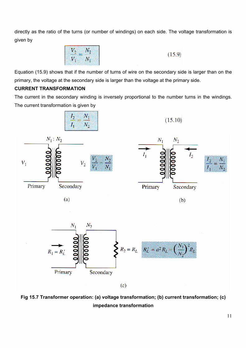
VOLTAGE TRANSFORMATION
As shown in Fig. 15.7a, the transformer can step up or step down a voltage applied to one side
11
directly as the ratio of the turns (or number of windings) on each side. The voltage transformation is
given by
Equation (15.9) shows that if the number of turns of wire on the secondary side is larger than on the
primary, the voltage at the secondary side is larger than the voltage at the primary side.
CURRENT TRANSFORMATION
The current in the secondary winding is inversely proportional to the number turns in the windings.
The current transformation is given by
Fig 15.7 Transformer operation: (a) voltage transformation; (b) current transformation; (c)
impedance transformation

12
This relationship is shown in Fig. 15.7b. If the number of turns of wire on the secondary is greater
than that on the primary, the secondary current will be less than the current in the primary.
IMPEDANCE TRANSFORMATION
Since the voltage and current can be changed by a transformer, impedance ‘seen’ from either side
(primary or secondary) can also is changed. As shown in Fig.15.7c, impedance RL is connected
across the transformer secondary. This impedance is changed by the transformer when viewed at the
primary side (R¯L ). This can be shown as follows:
If we define a =N1/N2, where a is the turns ratio of the transformer, the above equation becomes
We can express the load resistance reflected to the primary side as:
Where R¯L is the reflected impedance, as shown in Eq. (15.12), the reflected impedance is related
directly to the square of the turns ratio. If the number of turns of the secondary is smaller than that of
the primary, the impedance seen looking into the primary is larger than that of the secondary by the
square of the turns ratio
EXAMPLE 15.2
Calculate the effective resistance seen looking into the primary of a 15: 1 transformer connected to an
8-Ω load
Solution
EXAMPLE 15.3
What transformer turns ratio is required to match a 16-Ω speaker load so that the effective load
resistance seen at the primary is 10 kΩ?
Solution

13
Operation of Amplifier Stage
DC LOAD LINE
The transformer (dc) winding resistance determines the dc load line for the circuit of Fig. 15.6,
Typically, this dc resistance is small (ideally 0 Ω) and, as shown in Fig. 15.8, a 0-Ω dc load line is a
straight vertical line,
Fig 15.8 Load lines for class A transformer-coupled amplifier

14
A practical transformer winding resistance would be a few ohms, but only the ideal case will be
considered in this discussion. There is no dc voltage drop across the 0-Ω dc load resistance, and load
line is drawn straight vertically from the voltage point, VCEQ =VCC
QUIESCENT OPERATING POINT
The operating point in the characteristic curve of Fig. 15.8 can be obtained graphically at the point of
intersection of the dc load line and the base current set by the circuit. The collector quiescent current
can then be obtained from the operating point in class A operation, keep in mind that the dc bias point
sets the conditions for the maximum undistorted signal swing for both collector current and collector-
emitter voltage. If the input signal produces a voltage swing less than the maximum possible. The
efficiency of the circuit at that time will be less than 25%. The dc bias point is therefore important in
setting the operation of a class A series-fed amplifier
AC LOAD LINE
To carry out ac analysis, it is necessary to calculate the ac load resistance "seen" looking into the
primary side of the transformer, then draw the ac load line on the collector characteristic. The
reflected load resistance (R¯L ) is calculated using Eq. (15.] 2) using the value of the load connected
across the secondary (RL ) and the turns ratio of the transformer. The graphical analysis technique
then proceeds as follows. Draw the ac load line so that it passes through the operating point and has
a slope equal to -1/ R¯L ( the reflected load resistance), the load line slope being the negative
reciprocal of the ac load resistance. Notice that the ac load line shows that the output signal swing
can exceed the value of V cc. In fact, the voltage developed across the transformer primary can be
quite large. It is therefore necessary after obtaining the ac load line to check that the possible voltage
swing does not exceed transistor maximum ratings
SIGNAL SWING AND OUTPUT AC POWER
Figure 15.9 shows the voltage and current signal swings from the circuit of Fig. 15.6. From the signal
variations shown in Fig. 15.9, the values of the peak-to-peak signal swings are
The ac power developed across the transformer primary can then be calculated using

15
The ac power calculated is that developed across the primary of the transformer. As summing an
ideal transformer (a highly efficient transformer has an efficiency of well over 90%), the power
delivered by the secondary to the load is approximately that calculated using Eq. (15.13). The output
ac power can also be determined using the voltage delivered to the load.
Fig 15.9 Graphical operation of transformer-coupled class A amplifier
For the ideal transformer, the voltage delivered to the load can be calculated using Eq. (15.9):
The power across the load can then be expressed as
and equals the power calculated using Eq. (l5.5c).
Using Eq. (15.10) to calculate the load current yields
With the output ac power then calculated using

16
EXAMPLE 15.4
Calculate the ac power delivered to the 8-Ω speaker for the circuit of Fig.15.10. The circuit
component values result in a dc base current of 6 mA, and the input signal ( Vi ) results in a peak
base current swing of 4 mA.
Fig 15.10 Transformer-coupled class A amplifier for Example 15.4
Solution
The dc load line is drawn vertically (see Fig. 15.11) from the voltage point:
For IB = 6 mA, the operating point on Fig. 15.11 is
The effective ac resistance seen at the primary is
The ac load line can then be drawn of slope -1/72 going through the indicated operating point. To
help draw the load line, consider the following procedure. For a current swing of
Mark a point (A):

17
Fig 15.11 Transformer-coupled class A transistor characteristic for Examples 15.4 and 15.5: (a)
device characteristic; (b) dc and ac load lines
Connect point A through the Q-point to obtain the ac load line. For the given base current swing of 4
mA peak, the maximum and minimum collector current and collector-emitter voltage obtained from
Fig. 15.11 are
The ac power delivered to the load can then be calculated using Eq. (15.13):
Efficiency
So far we have considered calculating the ac power delivered to the load. We next consider the input
power from the battery, power losses in the amplifier, and the over all efficiency of the transformer-
coupled class A amplifier. The input (dc) power obtained from the supply is calculated from the supply
dc voltage and average power drawn from the supply:

18
For the transformer-coupled amplifier, the power dissipated by the transformer is small ( due to small
dc resistance of a coil) and will be ignored in the present calculation. Thus the only power loss
considered here is that dissipated by the power transistor and calculated using
Where P Q is the power dissipated as heat. While the equation is simple, it is nevertheless significant
when operating a class A amplifier. The amount of power dissipated by the transistor is the difference
between that drawn from the dc supply (set by the bias point) and the amount delivered to the ac
load. When the input signal is very small, with very little ac power delivered to the load, the maximum
power is dissipated by the transistor. When the input signal is larger and power delivered to the load
is larger, less power is dissipated by the transistor. In other words, the transistor of a class A amplifier
has to work hardest (dissipate the most power) when the load is disconnected from the amplifier, and
the transistor dissipates the least power when the load is drawing maximum power from the circuit.
EXAMPLE 15.5
For the circuit of Fig. 15.10 and results of Example 15.4, calculate the dc input power. Power
dissipated by the transistor, and efficiency of the circuit for the input signal of Example 15.4.
Solution
The efficiency of the amplifier is then
MAXIMUM THEORETICAL EFFICIENCY
For a class A transformer-coupled amplifier, the maximum theoretical efficiency goes up to 50%.
Based on the signals obtained using the amplifier, the efficiency can be expressed as
The larger the value of VCEmax, and the smaller the value of VCEmin the closer the efficiency approach

19
the theoretical limit of 50%.
EXAMPLE 15.6
Calculate the efficiency of a transformer-coupled class A amplifier for a supply of 12 V and outputs of
12V and outputs of:
(a) V (p) =12V.
(b) V (p) =6V.
(c) V (p) =2V.
Solution
Since VCEQ = VCC = 12 V, the maximum and minimum of the voltage swing are
Resulting in
Resulting in
Resulting in
Notice how dramatically the amplifier efficiency drops from a maximum of 50% for V(p) = VCC to
slightly over 1% for V(p) = 2V
15.4 CLASS B AMPLIFIER OPERATION
Class B operation is provided when the dc bias leaves the transistor biased just off, the transistor
turning on when the ac signal is applied. This is essentially no bias, and the transistor conducts
current for only one-half of the signal cycle. To obtain output for the full cycle of signal, it is necessary

20
to use two transistors and have each conduct on opposite half-cycles, the combined operation
providing a full cycle of output signal. Since one part of the circuit pushes the signal high during one
half-cycle and [he other part pulls the signal low during the other half-cycle, the circuit is referred [0 as
a push-pull circuit. Figure 15.12 shows a diagram for push-pull operation. An ,IC input signal is
applied to the push-pull circuit with each half operating on alternate half-cycles, the load then
receiving a signal for the full ac cycle. The power transistors used in the push-pull circuit are capable
of delivering the desired power to the load, and the class B operation of these transistors provides
greater efficiency than \\as possible using a single transistor in class A operation
Fig 15.12 Block representation of push-pull operation
Input (CD) Power
The power supplied to the load by an amplifier is drawn from the power supply (or power supplies;
see Fig. 15.13) that provides the input or de power. The amount of [his input power can be calculated
using
Where Idc is the average or dc current drawn from the power supplies. In class B operation, the
current drawn from a single power supply has the form of a full-wave rectified signal, while that drawn
from two power supplies has the form of a half-wave rectified signal from each supply. In either case,
the value of the average current drawn can be expressed as
Where I(p) is the peak value of the output current waveform. Using Eq. (15.18) in the power input
equation (Eq. 15.17) results in

21
Fig 15.13 Connection of push-pull amplifier to load: (a) using two voltage supplies; (b) using
one voltage supply
Output (AC) Power
The power delivered to the load (usually referred to as a resistance, RL) can be calculated using
anyone of a number of equations. If one is using an rms meter to measure the voltage across the
load, the output power can be calculated as
If one is using an oscilloscope, the peak, or peak-to-peak, output voltage measured can be used:
The larger the rms or peak output voltage, the larger the power delivered to the load
Efficiency
The efficiency of the class B amplifier can be calculated using the basic equation:

22
Using Eqs. (15.19) and (15.21) in the efficiency equation above results in
(Using l(p) = VL(p )/RL). Equation (15.22) shows that the larger the peak voltage, the higher the circuit
efficiency, up to a maximum value when VL(p) = VCC, this maximum efficiency then being
Power Dissipated by Output Transistors
The power dissipated (as heat) by the output power transistors is the difference between the input
power delivered by the supplies and the output power delivered to the load.
Where P2Q is the power dissipated by the two output power transistors. The dissipated 'power
handled by each transistor is then
EXAMPLE 15.7
For a class B amplifier providing a 20-V peak signal to a 16-Ω load (speaker) and a power supply of
VCC = 30 V, determine the input power, output power, and circuit efficiency
Solution
A 20-V peak signal across a 16-Ω load provides a peak load current of
The dc value of the current drawn from the power supply is then
And the input power delivered by the supply voltage is
The output power delivered to the load is

23
For a resulting efficiency of
Maximum Power Considerations
For class B operation, the maximum output power is delivered to the load when VL(p) = VCC
The corresponding peak ac current I(p) is then
So that the maximum value of average current from the power supply is
Using this current to calculate the maximum value of input power results in
The maximum circuit efficiency for class B operation is then
When the input signal results in less than the maximum output signal swing, the circuit efficiency is
less than 78.5%.
For class B operation, the maximum power dissipated by the output transistors does not occur at the
maximum power input or output condition. The maximum Power dissipated by the two output
transistors occurs when the output voltage across the load is

24
For a maximum transistor power dissipation of
EXAMPLE 15.8
For a class B amplifier using a supply of VCC = 30 V and driving a load of 16Ω.. Determine the
maximum input power, output power, and transistor dissipation
Solution
The maximum output power is
The maximum input power drawn from the voltage supply is
The circuit efficiency is then
As expected. The maximum power dissipated by each transistor is
Under maximum conditions a pair of transistors, each handling 5.7 W at most, can deliver 28.125 W
to a 16-Ω load while drawing 35.81 W from the supply.
The maximum efficiency of a class B amplifier can also be expressed as follows:
So that

25
EXAMPLE 15.9
Calculate the efficiency of a class B amplifier for a supply voltage of VCC = 24 V with peak output
voltages of:
(a)VL (p) =22V
(b)VL (p) =6V.
Solution
Notice that a voltage near the maximum [22 V in part (a)] results in an efficiency near the maximum,
while a small voltage swing [6 V in part (b)] still provides an efficiency near 20%. Similar power supply
and signal swings would have resulted in much poorer efficiency in a class A amplifier.
15.5 CLASS B AMPLIFIER CIRCUITS
A number of circuit arrangements for obtaining class B operation are possible. We will consider the
advantages and disadvantages of a number of the more popular circuits this section. The input
signals to the amplifier could be a single signal, the circuit then providing two different output stages,
each operating for one-half the cycle. If the input is in the form of two opposite polarity signals, two
similar stages, could be used, each operating on the alternate cycle because of the input signal. One
means of obtaining polarity or phase inversion is using a transformer, the transformer-coupled
amplifier having been very popular for a long time.
Opposite polarity input, can easily be obtained using an op-amp having two opposite outputs or using
a few op-amp stages to obtain two opposite polarity signals, an opposite polarity operation can also
be achieved using a single input and complementary transistors (npn and pnp, or nMOS and
pMOS).
Figure 15.14 shows different ways to obtain phase-inverted signals from a single input signal. Figure
l5.14a shows a center-tapped transformer to provide opposite phase signals. If the transformer is
exactly center-tapped, the two signals are exactly opposite in phase and of the same magnitude.

26
Fig 15.14 Phase-splitter circuit

27
The circuit of Fig. 15.14b uses a BJT stage with in-phase output from the emitter and opposite phase
output from the collector. If the gain is made nearly 1 for each output the same magnitude results.
Prob-ably most common would be using op-amp stages, one to provide an inverting gain of unity and
the other a non inverting gain of unity, to provide two outputs of the same magnitude but of opposite
phase.
Transformer-Coupled Push-Pull Circuits
The circuit of Fig. 15.15 uses a center-tapped input transformer to produce opposite polarity signals
to the two transistor inputs and an output transformer to drive the load in a push-pull mode of
operation described next.
During the first half-cycle of operation, transistor Q1 is driven into conduction whereas
transistor Q2 is driven off. The current I1 through the transformer results in the first half-cycle of signal
to the load. During the second half-cycle of the input signal. Q2 conducts whereas Q1 stays off, the
current I2 through the transformer resulting in the second half-cycle to the load, the overall signal
developed across the load then varies over the full cycle of signal operation.
Fig 15.15 Push-pull circuit
Complementary-Symmetry Circuits
Using complementary transistors (npn and pnp) it is possible to obtain a full cycle output across a
load using half-cycles of operation from each transistor, as shown in Fig. 15.16a.

28
Fig 15.16 Complementary-symmetry push-pull circuit
While a single input signal is applied to the base of both transistors, the transistors, being of opposite

29
type, will conduct on opposite half-cycles of the input. The npn transistor will be biased into
conduction by the positive half-cycle of signal, with a resulting half-cycle of signal across the load as
shown in Fig. 15.16b. During the negative half-cycle of signal, the pnp transistor is biased into
conduction when the input goes negative, as shown in Fig. 15.16c.
During a complete cycle of the input, a complete cycle of output signal is developed across the load.
One disadvantage of the circuit is the need for two separate voltage supplies. Another, less obvious
disadvantage with the complementary circuit is shown in the resulting crossover distortion in the
output signal (see Fig. 15.16d). Crossover distortion refers to the fact that during the signal crossover
from positive to negative (or vice versa) there is some nonlinearity in the output signal. This results
from the fact that the circuit does not provide exact switching of one transistor off and the other on at
the zero-voltage condition. Both transistors may be partially off so that the output voltage does not
follow the input around the zero-voltage condition biasing the transistors in class AB improves this
operation by biasing both transistors to be on for more than half a cycle.
A more practical version of a push-pull circuit using complementary transistors is shown in Fig. 15.17.
Note that the load is driven as the output of an emitter-follower so that the load resistance of the load
is matched by the low output resistance of the driving source. The circuit uses complementary
Darlington-connected transistors to provide higher output current and lower output resistance.
Fig 15.17 Complementary-symmetry push-pull circuit using Darlingtion transistors

30
Quasi-Complementary Push-Pull Amplifier
In practical power amplifier circuits, it is preferable to use npn transistors for both high-current-output
devices. Since the push-pull connection requires complementary devices, a pnp high-power transistor
must be used. A practical means of obtaining complementary operation while using the same,
matched npn transistors for the output is provided by a quasi-complementary circuit, as shown in Fig.
15.18.
Fig 15.18 Quasi-complementary push-pull transformer less power amplifier
The push-pull operation is achieved by using complementary transistors (Q1 and Q2) before the
matched npn output transistors (Q3 and Q4). Notice that transistors Q1 and Q3 form a Darlington
connection that provides output from a low-impedance emitter-follower. The connection of transistors
Q2 and Q4 forms a feedback pair, which similarly provides a low-impedance drive to the load. Resistor
R2 can be adjusted to minimize crossover distortion by adjusting the dc bias condition. The single
input signal applied to the push-pull stage then results in a full cycle output to the load. The quasi-
complementary push-pull amplifier is presently the most popular form of power amplifier
EXAMPLE 15.10
For the circuit of Fig. 15.19, calculate the input power, output power, and power handled by each
output transistor and the circuit efficiency for an input of 12 V rms.

31
Fig 15.19 Class B power amplifier for Example 15.10-15.12
Solution
The peak input voltage is
Since the resulting voltage across the load is ideally the same as the input signal (the amplifier has,
ideally, a voltage gain of unity),
and the output power developed across the load is
The peak load current is
from which the dc current from the supplies is calculated to be
so that the power supplied to the circuit is

32
The power dissipated by each output transistor is
The circuit efficiency (for the input of 12 V, rms) is then
EXAMPLE 15.11
For the circuit of Fig. 15.19, calculate the maximum input power, maximum output power, input
voltage for maximum power operation, and the power dissipated by the output transistors at this
voltage.
Solution
The maximum input power is
The maximum output power is
[Note that the maximum efficiency is achieved:]
To achieve maximum power operation the output voltage must be
and the power dissipated by the output transistors is then
EXAMPLE 15.12
For the circuit of Fig. 15.19, determine the maximum power dissipated by the output transistors and
the input voltage at which this occurs.
Solution
The maximum power dissipated by both output transistors is
33
This maximum dissipation occurs at
(Notice that at VL = 15.9 V the circuit required the output transistors to dissipate 31.66 W, while at VL
= 25 V they only had to dissipate 21.3 W.)
15.6 AMPLIFIER DISTORTION
A pure sinusoidal signal has a single frequency at which the voltage varies positive and negative by
equal amounts. Any signal varying over less than the full 360° cycle considered to have distortion. An
idea] amplifier is capable of amplifying a pure sinusoidal signal to provide a larger version, the
resulting waveform being a pure single-frequency sinusoidal signal. When distortion occurs the output
will not be an exact duplicate (except for magnitude) of the input signal.
Distortion can occur because the device characteristic is not linear, in which case nonlinear or
amplitude distortion occurs. This can occur with all classes of amplifier operation. Distortion can also
occur because the circuit elements and devices respond to the input signal differently at various
frequencies, this being frequency distortion. One technique for describing distorted but period
waveforms uses Fourier analysis, a method that describes any periodic waveform in terms of its
fundamental frequency component and frequency components at integer multiples-these components
are called harmonic components or harmonics. For example, a signal that is originally 1000 Hz
could result, after distortion, in a frequency component at 1000Hz (1 kHz) and harmonic components
at 2 kHz (2 X 1 kHz), 3 kHz (3 X 1 kHz), 4 kHz (4 X 1 kHz), and so on. The original frequency of 1
kHz is called the fundamental frequency; those at integer multiples are the harmonics. The 2-kHz
component is therefore called a second harmonic that at 3 kHz is the third harmonic, and so on. The
fundamental frequency is not considered a harmonic. Fourier analysis dose not allow for fractional
harmonic frequencies-only integer multiples of the fundamental.
Harmonic Distortion
A signal is considered to have harmonic distortion when there are harmonic frequency components
(not just the fundamental component). If the fundamental frequency has an amplitude, A1, and the nth
frequency component has an amplitude, An a harmonic distortion can be defined as
The fundamental component is typically larger than any harmonic component.
34
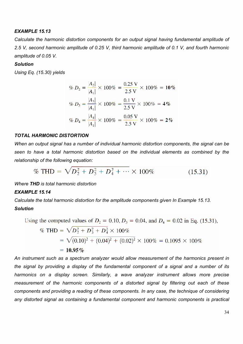
EXAMPLE 15.13
Calculate the harmonic distortion components for an output signal having fundamental amplitude of
2.5 V, second harmonic amplitude of 0.25 V, third harmonic amplitude of 0.1 V, and fourth harmonic
amplitude of 0.05 V.
Solution
Using Eq. (15.30) yields
TOTAL HARMONIC DISTORTION
When an output signal has a number of individual harmonic distortion components, the signal can be
seen to have a total harmonic distortion based on the individual elements as combined by the
relationship of the following equation:
Where THD is total harmonic distortion
EXAMPLE 15.14
Calculate the total harmonic distortion for the amplitude components given In Example 15.13.
Solution
An instrument such as a spectrum analyzer would allow measurement of the harmonics present in
the signal by providing a display of the fundamental component of a signal and a number of its
harmonics on a display screen. Similarly, a wave analyzer instrument allows more precise
measurement of the harmonic components of a distorted signal by filtering out each of these
components and providing a reading of these components. In any case, the technique of considering
any distorted signal as containing a fundamental component and harmonic components is practical

35
and useful. For a signal occurring in class AB or class B, the distortion may be mainly even
harmonics, of which the second harmonic component is the largest. Thus, although the distorted
signal theoretically contains all harmonic components from the second harmonic up. The most
important in terms of the amount of distortion in the classes presented above is the second harmonic.
SECOND HARMONIC DISTORTION
Figure 15.20 shows a waveform to use for obtaining second harmonic distortion. A collector current
waveform is shown with the quiescent, minimum, and maximum signal levels, and the time at which
they occur is marked on the waveform.
Fig 15.20 Waveform for obtaining second harmonic distortion
The signal shown indicates that some distortion is present. An equation that approximately describes
the distorted signal waveform is
The current waveform contains the original quiescent current ICQ, which occurs with. zero input signal;
an additional dc current IO, due to the nonzero average of the distorted signal the fundamental
component of the distorted ac signal, I1 ; and a second harmonic component I2, at twice the
fundamental frequency. Although other harmonics, are also present, only the second is considered
here. Equating the resulting current from Eq. (15.32) at a few points in the cycle to that shown on the
current waveform provides the following three relations:

36
Solving the preceding three equations simultaneously gives the following results:
Referring to Eq. (15.30), the definition of second harmonic distortion may be expressed as
Inserting the values of I1 and I2 determined above gives
In a similar manner, the second harmonic distortion can be expressed in terms of measured collector-
-emitter voltages:
EXAMPLE 15.5
Calculate the second harmonic distortion, if an output waveform displayed on an oscilloscope
provides the following measurements:
Solution

37
Power of Signal Having Distortion
When distortion does occur, the output power calculated for the undistorted signal is no longer
correct. When distortion is present, the output power delivered to the load resistor RC due to the
fundamental component of the distorted signal is
The total power due to all the harmonic components of the distorted signal can then be calculated
using
Thee total power can also be expressed in terms of the total harmonic distortion
EXAMPLE 15.16
For the harmonic distortion reading of D2 = 0.1, D3 = 0.02, and D4 = 0.01, with I1 =4 A and RC = 8Ω,
calculate the total harmonic distortion, fundamental power component, and total power.
Solution
The total harmonic distortion is
The fundamental power, using Eq. (15.35), is
The total power calculated using Eq. (15.37) is then
(Note that the total power is due mainly to the fundamental component even with 10% second
harmonic distortion.)

38
Graphical Description of Harmonic Components of Distorted Signal
A distorted waveform such as that which occurs in class B operation can be represented using
Fourier analysis as a fundamental with harmonic components. Figure 15.21a shows a positive half-
cycle such as the type that would result in one side of a class B amplifier.
Fig 15.21 Graphical representation of a distorted signal through the use of harmonic
components
Using Fourier analysis techniques, the fundamental component of the distorted signal can be
obtained, as shown in Fig. 15.21 b. Similarly, the second and third harmonic components can be
obtained and are shown in Fig. 15.21c and d, respectively. Using the Fourier technique, the distorted
waveform can be made by adding the fundamental and harmonic components, as shown in Fig.

39
15.21 e. In general, any periodic distorted waveform can be represented by adding a fundamental
component and all harmonic components, each of varying amplitude and at various phase angles