15 · 15 nal ol components 0 vol ... 40 high power passives fit emerging rf energy market ......
TRANSCRIPT

O
ctob
er 2015 M
icrowave Jo
urn
al
Passive & C
on
trol C
om
po
nen
ts V
ol. 58 • N
o. 10
October 2015Vol. 58 • No. 10
Founded in 1958
AnarenHigh Power
Passives
MVP
.com
OCTOBER COVER FINAL.indd 1 9/28/15 2:52 PM

FilterBank
AntennaSwitch Module
AntennaSwap Switch
AntennaTuner
Coupler
Diplexer
PA ModeSwitch
PowerAmplifier
2G
3GLTE
3GLTE
2G
SupplyModulator
TxHighBand
MODEM
+
TRANSCEIVER
TxLowBand
Rx LowBand
Rx HighBand
MIPI
RxDiversity
Rx DiversitySwitch
October 2015Vol. 58 • No. 10Passive and ControlComponentsmwjournal.com
Cover Feature
22 RF SOI: Revolutionizing RF System DesignPeter A. Rabbeni, Alvin Joseph, Theodore Letavic and Anirban Bandyopadhyay, GlobalFoundries
MVP: Most Valuable Product
40 High Power Passives Fit Emerging RF Energy Market Anaren Inc.
Technical Features
64 Engineered Substrates: The Foundation to Meet Current and Future RF RequirementsEric Desbonnets and Christophe Didier, Soitec
5 8 Y E A R S O F P U B L I S H I N G E X C E L L E N C E
10 MICROWAVE JOURNAL OCTOBER 2015
76 A Current-Reused GPS LNA In 0.2 µm RF SOI TechnologyRuofan DaiI, II, III, Yunlong ZhengI, II, Shichang ZouI, III, Weiran KongIII, State Key Laboratory of Functional Materials for Informatics, Shanghai Institute of Microsystem and Information Technology, Chinese Academy of SciencesI, University of Chinese Academy of SciencesII, Shanghai Huahong Grace Semiconductor Manufacturing Corp.III
88 Simple Synthesized Harmonic Matching Strategy in Broadband PA DesignYinjin Sun, Xiaowei Zhu and Fan Meng, Southeast University
100 Temperature Compensation of Microwave Resonators and Filters for Space ApplicationsDr. ing. Marco Lisi, European Space Agency
110 Frequency Agile DiplexerMarjan Grman, Iskra Sistemi
120 A Dual-Channel X-Band Receiver for MIMO SystemsWeichen Huang, Liang Ma, Zhiqiang Yu and Jianyi Zhou, State Key Laboratory of Millimeter Waves, Southeast University
CONTENTS
22
40 64
STEP 1 STEP 2Download the free Layar app from the iTunes (iOS) or Google Play (Android)
store.
Launch the app to view enhanced content on any page
with the logo.
STEP 3Frame the entire page in the screen and
tap to experience enhancements (tap screen again for full screen view).
AUGMENTED REALITY: HOW IT WORKS
Look for the Layar logo on participating pages. AR pages may expire after 30 days.
10M04 FINAL.indd 10 9/28/15 2:52 PM

017 Mark Your Calendar018 Coming Events045 Defense News049 International Report053 Commercial Market056 Around the Circuit
150 Catalog Update152 New Products158 Book End160 Advertising Index160 Sales Reps162 Fabs and Labs
12 MICROWAVE JOURNAL OCTOBER 2015
Product Features
134 PXIe Measurement Accelerator Speeds RF Power Amplifi er TestKeysight Technologies
142 VNAs Support Need for Higher FrequenciesCopper Mountain Technologies
144 Line-of-Sight Verifi cation Kit for Microwave Field EngineersSAF Tehnika
Tech Briefs
146 Effi cient, Broadband Distributed LO Driver Amplifi ersMarki Microwave Inc.
147 700 W HPA for Satellite UplinksCommunications & Power Industries LLC
149 Space-Saving Flange-Mount Probes INGUN USA Inc.
Departments
CONTENTS
Microwave Journal (USPS 396-250) (ISSN 0192-6225) is published monthly by Horizon House Publications Inc., 685 Canton St., Norwood, MA 02062. Periodicals postage paid at Norwood, MA 02062 and additional mailing offi ces.
Photocopy Rights: Permission to photocopy for internal or personal use, or the internal or personal use of specifi c clients, is granted by Microwave Journal for users through Copyright Clearance Center provided that the base fee of $5.00 per copy of the article, plus $1.00 per page, is paid directly to the Copyright Clearance Center, 222 Rosewood Drive, Danvers, MA 01923 USA (978) 750-8400. For government and/or educational classroom use, the Copyright Clearance Center should be contacted. The rate for this use is 0.03 cents per page. Please specify ISSN 0192-6225 Microwave Journal International. Microwave Journal can also be purchased on 35 mm fi lm from University Microfi lms, Periodic Entry Department, 300 N. Zeeb Rd., Ann Arbor, MI 48106 (313) 761-4700. Reprints: For requests of 100 or more reprints, contact Barbara Walsh at (781) 769-9750.
POSTMASTER: Send address corrections to Microwave Journal, PO Box 1143, Skokie, IL 60076 or e-mail [email protected]. Subscription information: (847) 763-4943. This journal is issued without charge upon written request to qualifi ed persons working in the RF & microwave industry. Other subscriptions are: domestic, $120.00 per year, two-year subscriptions, $185.00; foreign, $200.00 per year, two-year subscriptions, $370.00; back issues (if available) and single copies, $10.00 domestic and $20.00 foreign. Claims for missing issues must be fi led within 90 days of date of issue for complimentary replacement.
©2015 by Horizon House Publications Inc.Posted under Canadian international publications mail agreement #PM40612608
134 142
mwjournal.com STAFF
144
www.mwjournal.com
Printed in the USA
PUBLISHER: Carl Sheffres EDITOR: Patrick Hindle
TECHNICAL EDITOR: Gary LerudeMANAGING EDITOR: Jennifer DiMarco
ASSOCIATE TECHNICAL EDITOR: Cliff DrubinMULTIMEDIA STAFF EDITOR: Leslie Nikou
MULTIMEDIA STAFF EDITOR: Barbara Walsh CONSULTING EDITOR: Harlan Howe, Jr.
CONSULTING EDITOR: Frank BashoreCONSULTING EDITOR: David Vye
CONSULTING EDITOR: Raymond PengellyELECTRONIC MARKETING MANAGER:
Chris StanfaCLIENT SERVICES MANAGER:
Kristen AndersonEVENT COORDINATOR: Jacqueline Williams
AUDIENCE DEVELOPMENT MANAGER: Carol Spach
TRAFFIC MANAGER: Edward KiesslingDIRECTOR OF PRODUCTION & DISTRIBUTION:
Robert BassART DIRECTOR: Janice Levenson
GRAPHIC DESIGNER: Sachiko Stiglitz
EUROPE
INTERNATIONAL EDITOR: Richard MumfordOFFICE MANAGER: Nina Plesu
CORPORATE STAFF
CEO: William M. BazzyPRESIDENT: Ivar Bazzy
VICE PRESIDENT: Jared Bazzy
EDITORIAL REVIEW BOARD Dr. I.J. Bahl
F.M. BashoreDr. C.R. BoydM. GoldfarbJ.L. Heaton
Dr. G. HeiterH. Howe, Jr.Dr. T. Itoh
Dr. J. LaskerDr. S. Maas
Dr. G.L. MatthaeiDr. D.N. McQuiddy
Dr. J.M. OsepchukR. Pengelly
Dr. Ajay K. PoddarDr. J. RautioDr. U. Rohde
Dr. P. StaeckerF. Sullivan
D. SwansonDr. R.J. TrewG.D. Vendelin
D. VyeProf. K. Wu
EXECUTIVE EDITORIAL OFFICE685 Canton Street, Norwood, MA 02062
Tel: (781) 769-9750FAX: (781) 769-5037
e-mail: [email protected]
EUROPEAN EDITORIAL OFFICE16 Sussex Street, London SW1V 4RW, England
Tel: Editorial: +44 207 596 8730 Sales: +44 207 596 8740FAX: +44 207 596 8749
SUBSCRIPTION SERVICESSend subscription inquiries and address changes to:
Tel: (847) 763-4943e-mail: [email protected]
10M04 FINAL.indd 12 9/29/15 2:07 PM

RF SOI: Revolutionizing RF System DesignPeter A. Rabbeni, Alvin Joseph, Theodore Letavic and Anirban BandyopadhyayGlobalFoundries, Santa Clara, Calif.
RF SOI has taken the mobile RF world by storm recently in helping to solve the challenges that go along with ensuring
users seamless, always available connectivity and access to the power of the Internet from virtually anywhere. The introduction of cloud computing is driving user expectations even higher. RF SOI is well positioned to become the innovation platform for delivering im-proved performance, lowering overall system costs needed to accommodate these rising ex-pectations and staying ahead of the ever evolv-ing network requirements. This article exam-ines the industry trends that got us here, what’s next and how RF SOI can improve the perfor-mance of RF systems.
THE WIRELESS LANDSCAPERich content delivery to users has grown
exponentially over the last five years. In de-veloped countries, compressed high-definition video streaming over the Internet through ser-vices such as Netflix and Hulu is already nearly ubiquitous. The need for greater bandwidth will only increase as demands for higher quality content gives way to true uncompressed 1080p and 4K video delivery in the future. Cisco fore-casts that by 2019, global Internet traffic will triple over 2014 levels, rising to 168 exabytes (EB) per month, a cumulative annual increase of over 23 percent.1
The rise of cloud computing now allows this data rich content to be accessed anywhere and, more importantly, to be accessed anywhere while mobile. For an enhanced user experi-ence, delivery of this content can be achieved only through higher data rates — within the confines of the available spectrum — with as low latency as possible. Demand for higher data rates is one of the main drivers for the evolution of current wireless communica-tion standards. Over the last five years, both cellular and Wi-Fi have advanced at unprec-edented rates. Cellular standards have transi-tioned from 2G/2.5G to 3G/4G, and now 4G/
22 MICROWAVE JOURNAL n OCTOBER 2015
COVER FEATUREINVITED PAPER
s Fig. 1 Global mobile data traffic forecast.2
30
25
20
15
10
5
02014 2015 2016 2017 2018 2019
57%CAGR
2.5 4.26.8
10.7
16.1
24.3
Exab
ytes
per
Mon
th
_10M27 Final PROOF.indd 22 9/28/15 2:52 PM

24 MICROWAVE JOURNAL n OCTOBER 2015
CoverFeature
ous regions have surfaced, creating a hodge-podge of fractured bands that carriers must deal with as part of net-work deployment. The emergence of LTE as a cellular standard has made this evident; LTE now has defined more than 40 bands, many of which are non-contiguous, currently cover-ing 700 MHz to 2.6 GHz, with propos-als to add more spectrum both above and below this range. The provisions within the standard enable high data rate capability (>300 Mbps downlink and up to 75 Mbps uplink) through the use of various techniques, includ-ing higher order orthogonal frequency division modulation (OFDMA) and carrier aggregation. These provisions are enabled to achieve as much spec-tral efficiency as possible to reach the target data throughput and serve as many users as possible within a given regional frequency plan.
Similar provisions for data rate ex-pansion in Wi-Fi networks not only provide a better user experience for data-rich content but also offer a po-tential means to augment cellular network capacity through offloads to carrier grade Wi-Fi access points. For example, the IEEE 802.11ac Wi-Fi standard has seen significant adoption (projected 13 percent CAGR over 2014-20) since its introduction and, with the Wave 2 specifications, prom-ises data rates up to 3.5 Gbps through the use of multiple-input-multiple-output (MIMO) and channel bonding techniques.4
CAN’T WE ALL JUST BE FRIENDS?Enabling the high data rate sup-
ported by LTE is driving the complex-ity we see today in all segments of the RF interface – the front-end module (FEM), in particular, but also the RF transceiver and baseband processor. The complexity in the FEM originates primarily from four sources:1. Increasing number of bands sup-
ported per handset (ranging from 2 to 18 LTE bands in addition to legacy 2G/3G bands)
2. Introduction of high frequency bands (6 bands at 2.5 GHz and above)
3. High peak to average power ratio (PAPR) from OFDM (also used in other UMTS technologies and in Wi-Fi), where the PAPR can be up to 11.5 dB5
4. Carrier aggregation (CA) which
traffic combined. To put this in perspec-tive, this amount of data is equivalent to transmitting the entire text and me-dia content of the Library of Congress over 70,000 times every month.
Achieving these predictions is not hard to understand given the rapid global adoption of LTE in cellphones (2014-19 CAGR = 26 percent). Al-though the overall
mobile handset market growth has begun to plateau (CAGR = 4 percent), it is actually demand for LTE-capable handsets that is sustaining the growth of the overall mobile handset market. This clearly demonstrates the transi-tion from devices supporting older legacy standards to devices that can provide a richer user experience, as shown in Figure 2.
Enabling increased data rates in mobile devices does not come easily. Challenges in working within the al-located cellular spectrum across vari-
LTE. The same holds true for Wi-Fi standards, which have evolved from their humble 802.11a/b/g beginnings as a replacement for 56 Kbps wired modems to today’s 802.11ac, rivaling CAT6 wired Ethernet connections and promising wireless Gbps speeds.
Trends in mobile data consump-tion parallel this transition. Cisco also predicts that total global mobile data traffic will grow 10-fold between 2014 and 2019, to more than 24 EB per month (see Figure 1) — a growth rate nearly double that of global data
s Fig. 2 Global wireless handset forecast.3
2.5
2.0
1.5
1.0
0.5
0
2/2.5G3GLTE
2014 2015 2016 2017
Total CAGR 4%
LTE Phone C
AG
R 26%
2018 2019
Bill
ions
of
Uni
ts
s Fig. 3 4G/LTE RF FEM architecture.6
FilterBank
AntennaSwitch Module
AntennaSwap Switch
AntennaTuner
Coupler
Diplexer
PA ModeSwitch
PowerAmplifier
2G
3GLTE
3GLTE
2G
SupplyModulator
TxHighBand
MODEM
+
TRANSCEIVER
TxLowBand
Rx LowBand
Rx HighBand
MIPI
RxDiversity
Rx DiversitySwitch
_10M27 Final PROOF.indd 24 9/28/15 2:52 PM

26 MICROWAVE JOURNAL OCTOBER 2015
CoverFeature
AMPLIFIERS
FROM 500 MHZ TO 110 GHZ, SIMPLE OR COMPLEXWE CAN DESIGN THE COMPONENTS YOU WANT
TRANSCEIVERS & FREQUENCY CONVERTERS
CUSTOMASSEMBLIES
WWW.NORDENGROUP.COM PHONE (530) 642-9123 FAX (530) 642-9420
cycles from the baseband/applications processor to deliver the necessary control to the PA bias controller to ac-curately track the modulation signal envelope. For improving PA linear-ity, digital predistortion (DPD) tech-niques have also been employed in cellular applications. These DPD and ET techniques are emerging in Wi-Fi power amplifi er applications as well, signifi cant challenges that need to be addressed.
The physical limitation of today’s mobile device form factors have also contributed to the ever changing de-mands of today’s wireless standards. The Wheeler limit relates the physi-cal dimensions of an antenna struc-ture to its resultant gain and band-width. Achieving fl at broadband gain and directivity from an antenna, not much larger than a stick of gum, over all 40+ LTE frequency bands is very
cy components drain power from the desired fundamental signal and may also cause saturation in the receiver LNA, depending on power level.
The high peak-to-average ratio of the modulated LTE signal requires that all FEM components have highly linear characteristics. Reduced linear-ity anywhere in the signal chain re-quires that the signal be “backed-off” in terms of the average power incident to the device to remain within the lin-ear operating region of the entire sig-nal path. Reduced linearity inherently translates to lower power delivered by the mobile device to the base station on transmit and lower power than can be processed by the receiver base-band processor. Both scenarios can cause dropped calls.
Although not immediately intui-tive, signal back-off also affects bat-tery life. Power amplifi ers tend to be most effi cient when operated at saturated power levels; however, these conditions are worst for linear-ity. Therefore, for linear transmission, one needs to back off power levels, causing amplifi ers to be less effi cient. Special techniques such as average power tracking (APT) and envelope tracking (ET) have been employed to adjust the PA bias on a real-time ba-sis according to the envelope of the modulated output waveform, so that the PA always operates near optimum effi ciency. These techniques have been implemented with some suc-cess. It requires additional computing
further enhances the complexity due to the low effi ciency of hand-set antennas of limited size and the demand of long battery life.The architecture of one of today’s
advanced LTE capable smartphones demonstrates this complexity, as shown in the example block diagram of Figure 3. Support for multiple bands in a mobile device requires a complex array of fi lters and switches with high throw counts to route sig-nals to and from the antenna to the main RF transceiver/baseband for Tx/Rx processing. Within this array of fi lters and switches, careful consider-ation must be given to path loss, isola-tion, stopband rejection and linearity to ensure the fi delity of the signal be-ing processed.
The RF switch plays an important role in this architecture by providing high electrical isolation between the “on” channel and other “off” chan-nels, while protecting the highly sen-sitive receiver channels from the high power transmitter signal. The high peak power of the LTE transmitter (which can reach one watt or more) also generates harmonic frequency components and non-harmonic, inter-modulation frequency components, due to the nonlinear behavior of any of the FEM components in the signal path. These include the RF switches and other active and passive compo-nents such as tuners, low noise am-plifi ers (LNA), power amplifi ers (PA) and fi lters. These undesired frequen-
CoverFeature
Fig. 4 Peak-to-peak voltage with high antenna VSWR.7
Antenna
PA
40 to 80 Vpp
LNA
_10M27 Final PROOF.indd 26 9/28/15 2:53 PM
28 MICROWAVE JOURNAL n OCTOBER 2015
CoverFeature
ing either of these requirements must operate efficiently and with good re-ception characteristics. This can only be achieved by improving these key figures of merit (loss, isolation, linear-ity) even further.
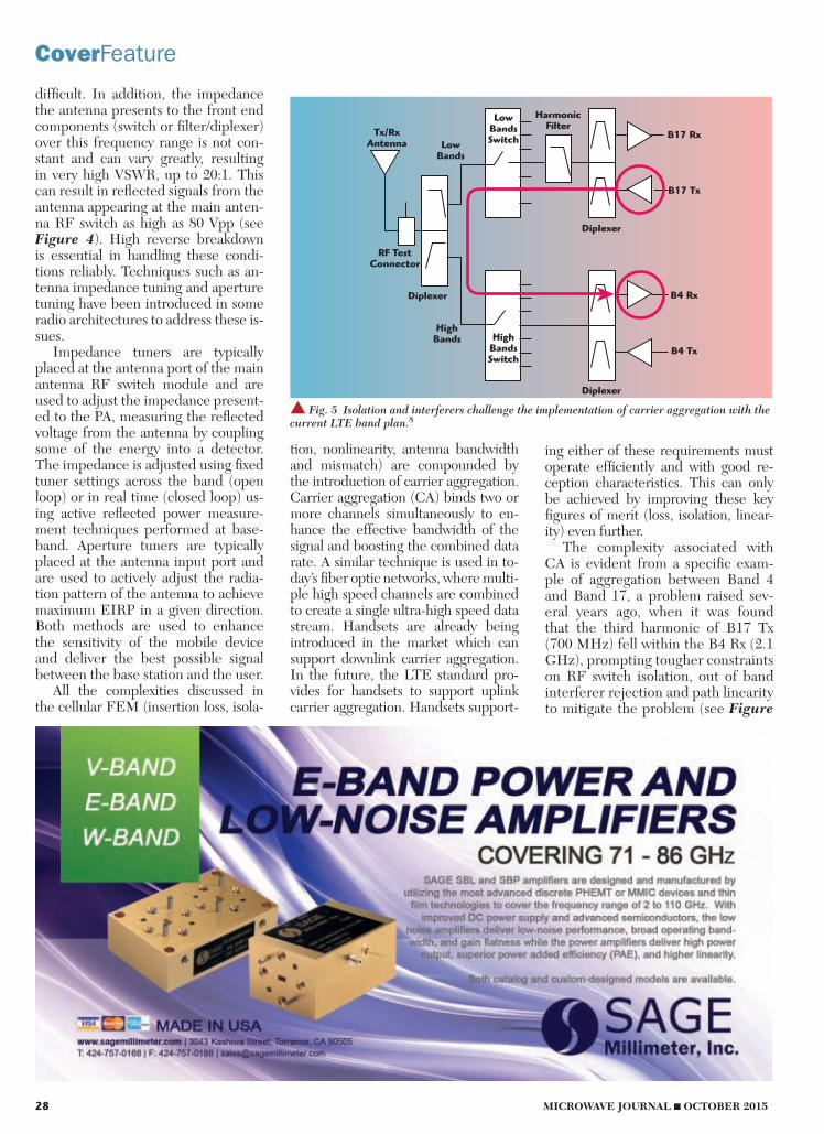
The complexity associated with CA is evident from a specific exam-ple of aggregation between Band 4 and Band 17, a problem raised sev-eral years ago, when it was found that the third harmonic of B17 Tx (700 MHz) fell within the B4 Rx (2.1 GHz), prompting tougher constraints on RF switch isolation, out of band interferer rejection and path linearity to mitigate the problem (see Figure
tion, nonlinearity, antenna bandwidth and mismatch) are compounded by the introduction of carrier aggregation. Carrier aggregation (CA) binds two or more channels simultaneously to en-hance the effective bandwidth of the signal and boosting the combined data rate. A similar technique is used in to-day’s fiber optic networks, where multi-ple high speed channels are combined to create a single ultra-high speed data stream. Handsets are already being introduced in the market which can support downlink carrier aggregation. In the future, the LTE standard pro-vides for handsets to support uplink carrier aggregation. Handsets support-
difficult. In addition, the impedance the antenna presents to the front end components (switch or filter/diplexer) over this frequency range is not con-stant and can vary greatly, resulting in very high VSWR, up to 20:1. This can result in reflected signals from the antenna appearing at the main anten-na RF switch as high as 80 Vpp (see Figure 4). High reverse breakdown is essential in handling these condi-tions reliably. Techniques such as an-tenna impedance tuning and aperture tuning have been introduced in some radio architectures to address these is-sues.
Impedance tuners are typically placed at the antenna port of the main antenna RF switch module and are used to adjust the impedance present-ed to the PA, measuring the reflected voltage from the antenna by coupling some of the energy into a detector. The impedance is adjusted using fixed tuner settings across the band (open loop) or in real time (closed loop) us-ing active reflected power measure-ment techniques performed at base-band. Aperture tuners are typically placed at the antenna input port and are used to actively adjust the radia-tion pattern of the antenna to achieve maximum EIRP in a given direction. Both methods are used to enhance the sensitivity of the mobile device and deliver the best possible signal between the base station and the user.
All the complexities discussed in the cellular FEM (insertion loss, isola-
s Fig. 5 Isolation and interferers challenge the implementation of carrier aggregation with the current LTE band plan.8
LowBands
HighBands
Tx/RxAntenna
RF TestConnector
Diplexer
Diplexer
Diplexer
HighBandsSwitch
LowBandsSwitch
HarmonicFilter
B17 Rx
B17 Tx
B4 Rx
B4 Tx
_10M27 Final PROOF.indd 28 9/28/15 2:53 PM
30 MICROWAVE JOURNAL OCTOBER 2015
CoverFeature
WHY RF SOI AND WHY NOW?It is well known that RF SOI has
established itself as the technology of choice for cellular and Wi-Fi RF switches in many applications. In the early days of 3G/4G adoption, a new technology was needed that could achieve the same or similar perfor-mance in terms of Ft, mobility and breakdown voltage with suffi cient manufacturing capacity to meet the
overlapping channels, particularly in the 2.5 GHz Band. Together these requirements put signifi cant pressure on overall front-end performance to minimize power consumption and achieve good reception.
In an access point, 802.11ac prom-ises a peak data rate of 6.7 Gbps with 160 MHz bandwidth and an 8 × 8 MIMO confi guration, while compat-ible terminal devices will push 1 Gbps with a 2 × 2 MIMO confi guration. These requirements put a signifi cant burden on the PA effi ciency and total solution size, which favors silicon in-tegration. In the future, to drive >10 Gbps data rates, the standards being discussed today will either push im-proved spectral effi ciency of 802.11ac transmission (as is being proposed in 802.11ax) or a move to a higher fre-quency band (802.11ad). For the fore-seeable future, the Wi-Fi data rate re-quirements will place signifi cant pres-sure on overall front-end effi ciency to minimize power consumption and module size.
5). Even if the Rx frequency is not a multiple (second, third harmonic, etc.) of the Tx frequency aggrega-tion bands, there can be interference for carrier aggregation frequency pair combinations where the Rx fre-quency coincides with one of the in-ter-modulation frequencies of the Tx band. There are a number of carrier aggregation band pairs which fall into this category.
WHAT ABOUT WI-FI?A similar complexity in FEM ar-
chitectures is seen in 802.11ac Wi-Fi. MIMO channel binding and beam-forming techniques are leveraged to maximize signal fi delity, and each of these techniques has its own chal-lenges in implementation. Com-pared to cellular, Wi-Fi operates at reduced signal power levels (20 dBm maximum user equipment transmit-ted power compared to 23 dBm for LTE), since coverage is over a shorter distance. However, these systems use complex modulation to support the high data rate (up to 256 QAM in 802.11ac) and a high carrier frequen-cy (5.8 GHz), which require careful system design. The linearity require-ment for Wi-Fi 802.11ac power am-plifi ers is very stringent because of high PAPR and EVM requirements (< 1.8 percent Tx for 256 QAM con-stellation density). The LNA noise fi gure and linearity requirements (for RF switches as well) are also stringent due to high levels of interference of
Fig. 6 RF SOI device stacking.9
VGATE
Rgate ��
P1 P2
RSD RSD RSD RSD RSD RSD
RGRGRGRGRGRG
RGC2�f(Cgs + Cgd)
1
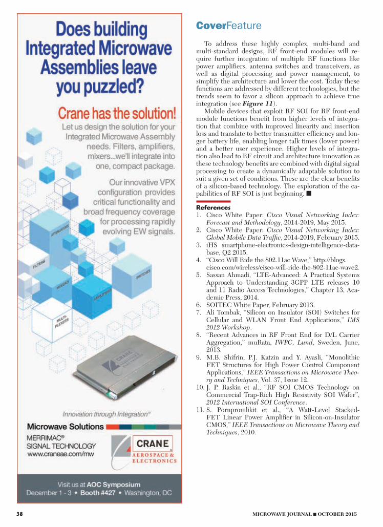
Fig. 7 10 V peak-to-peak input across a 4-stack SOI FET, with almost equal voltage drop across the drain nodes of each FET (D1, D2 and D3).7
1062
–2–6
–103.02.52.01.51.00.50
Time (ns)
Vin D1 D2 D3 Vout
Volt
age
(V)
_10M27 Final PROOF.indd 30 9/28/15 2:53 PM

32 MICROWAVE JOURNAL OCTOBER 2015
CoverFeature
Broadband Hybrid Antenna Includes: GSM, EGSM, AWS, DCS, PCS, IMTCost Effective & No Matching
Contact us for a free quote!
Includes: GSM, EGSM, AWS, DCS, PCS, IMTCost Effective & No Matching
Contact us for a free quote!
Tunable PWB
Metal Stamping
ing reduction in BVdss. Reduction in BVdss requires a larger device stack height and chip area in order to main-tain the high voltage handling capabil-ity. The off state capacitance (Coff) is another key metric in switch design and determines the off state isolation the device can achieve. Reduction in Coff to achieve greater isolation can be challenging and must employ a va-riety of techniques including junction engineering, device layout and metal stack optimization. Continual reduc-tion in the Ron Coff product while maintaining a reasonable BVdss has allowed complex switch products to be designed.
With a high quality RF switch that
ture9 that RF SOI on a high resistivity substrate with suffi ciently high gate resistors allow the FET body termi-nals to fl oat and allow multiple FET devices to be stacked in order to han-dle high voltage, high power condi-tions (see Figure 6).
By combining these inherent prop-erties of RF SOI along with the use of proper bias network design, one can achieve the correct voltage divi-sion across the stack in the off state and very low resistance in the on state (Ron) for low insertion loss (see Fig-ure 7). Intrinsic device Ron reduction is achieved fundamentally by lowering channel length, but this must be care-fully balanced with the correspond-
expected market demand at a lower cost. Until that point, GaAs PHEMT and PIN diode technologies were used for the RF switch function. The key characteristics that have solidifi ed RF SOI’s role in mobile FEMs are:1. Device stacking ability for higher
voltage handling2. Low on-resistance (Ron) for re-
duced insertion loss3. Low off-capacitance (Coff) and
substrate parasitics for high isola-tion and high Q
4. Logic and control integration5. Low cost and improved economics
over III-V technologies6. Mainstream silicon manufacturing
It has been covered in the litera-
Fig. 8 16-state variable capacitor array.7
RF 1
V+DD
C0 C1 C2 C3
V–DD
RF 2
Control/Supply
Fig. 9 Harmonic distortion of a coplanar transmission line, comparing HR-SOI to HR-SOI with a trap-rich layer.10
–60
–70
–80
–90
–100
–110
–120
–60
–70
–80
–90
–100
–110
–120100–10–20
Pou
t (d
Bm
)
Pou
t (d
Bm
)
Pin (dBm)
2nd Harmonic 3rd Harmonic
HR-SOIHR-SOI + Trap-Rich
HR-SOIHR-SOI + Trap-Rich
100–10–20
Pin (dBm)
_10M27 Final PROOF.indd 32 9/28/15 2:53 PM

34 MICROWAVE JOURNAL OCTOBER 2015
CoverFeature
Instruments Corporation
[email protected] [email protected]
Quantum SMART ACCELERATING YOUR TIME-TO-MARKET
Shifting the Standard of the Technology Development Roadmap, “Quantum SMART” is Accel-RF’s test fixture solution that enables accelerated product launch and improved return on investment (ROI). Quantum SMART enables concurrent testing for reliability validation, performance characterization and product qualification through RF-biased burn-in and product functional testing. The platform is software controlled through a standard user-interface, capable of “active” control and monitoring of bias, RF, and temperature through embedded firmware.
can handle high power levels and achieve low insertion loss with high isolation, one can begin to imagine other applications where this de-vice can be used. By combining RF switches and capacitors in series or in shunt into an array, a selectable or tunable high Q capacitor bank can be created, as shown in Figure 8, that can be used as a dynamic or variable tuning element. Many of today’s RF SOI technologies have high qual-ity metal-insulator-metal (MIM) and metal-oxide-metal (MOM) capacitors with reasonably high density (>2 fF/µm2) and high breakdown voltages to support large standing wave signals. The combination of MIM/MOM ca-pacitors and RF switches makes tun-ers possible, leading to the adoption of RF SOI for applications such as antenna impedance matching or an-tenna aperture tuning to address the antenna bandwidth and impedance variability problems.
Both of the applications described require an element of digital control to select a given switch confi guration or tuner state. In GaAs or other III-V technologies, this t ypically requires a separate CMOS controller chip to be paired with the GaAs device to dy-namically adjust the device state based on commands from the baseband pro-cessor. RF SOI allows the complete monolithic integration of the control-ler element and the RF function into a single chip, thus reducing cost, space and overall system complexity.
Due to the power levels involved, each of the applications described re-quires very high linearity and low har-monic response in order to minimize the creation of distortion products in high power, multi-carrier conditions. Today’s LTE system specifi cations require any harmonics generated by the RF switch to be >70 dB below the main carrier signal. Increased FET breakdown voltage allows reducing stack height and improving insertion loss and related harmonic genera-tion. However, another component of non-linearity is associated with sur-face charge recombination in the sub-strate, where high power RF signals can induce the creation of a parasitic conduction layer in the SOI substrate silicon/buried oxide (BOX) interface. RF signals may couple to this parasitic layer and modulate its conduction characteristics. This dynamic has been
Fig. 10 Comparison of key FEM technologies.
Performance Metric
Insertion Loss
Linearity
Passives Q
Breakdown Voltage
Thermal Conductivity
Digital Integration
Cost
GaAs SiGe RF SOI CMOS
Fig. 11 RF FEM technology trends.
PowerAmplifiers PA
Si LDMOS CMOS SiGe?
GaAs
GaAs
GaAs
2010 2012 2014 2016 2018 2020
RF SOI
RF SOI (LNA+Switch)
SiGe (LNA only)
RF SOI
RF SOI
SAW
BAW
RF MEMS?
RF MEMS?
Antenna/Mode Switches
AntennaTuners
Filter,Duplexers
LNA,LNA+Switch
_10M27 Final PROOF.indd 34 9/28/15 2:53 PM

36 MICROWAVE JOURNAL OCTOBER 2015
CoverFeatureMISSION CRITICAL
HIGHPOWER
SWITCHESu 10MHz to 18GHzu 1 watt to >10kWu SPST to T/R to SPnTu Built in fast driveru Speeds to 50ns
RF LIMITERSu SMT, Coax or W/Gu Active and passive
limitingu High CW and peak
poweru Low flat leakageu Optional: BITE,
indicator out
MULTI-FUNCTION MODULESu LNA limitersu Switch limitersu Switch matrixu T/R module
(T/R-Limiter/LNA)
LIMITER
ANT
TO COMTECH PST AMP
LNA
T/R
MIL-SPEC Compliant Solutions
H i l l E n g i n e e r i n g D i v i s i o n
The Power of Positive Partnering
978.887.5 754 • sa l es@h i l l en g.com
www.comtechpst.com/hill ISO 9001:2000
addressed through various substrate treatments, such as charge trap-injection, which minimize the creation of this parasitic layer at the interface. This has resulted in better than 15 dB improvement in device linearity performance over standard high resistivity substrates without these treatments (see Figure 9).
RF SOI has enabled the integration of two other criti-cal components of the FEM: LNAs and PAs. The noise fi gure and gain performance of an LNA is driven by the ft, fmax and gate resistance of the FET. SOI provides a very low capacitance device thereby helping both ft and fmax. Since the early introduction of RF SOI, the Wi-Fi FEM has widely deployed the use of both switches and LNAs integrated on a single IC. With the advent of car-rier aggregation in LTE cellular applications, improved LNA performance for both main Tx/Rx and diversity Rx antenna paths is desired. This presents an opportunity for RF SOI to allow the integration of optimized switches and LNAs in the cellular FEM as well. Power amplifi ers, on the other hand, need high ft and high breakdown volt-ages. FET stacking concepts have been demonstrated on high resistivity (HR) substrate RF SOI devices in the lit-erature to provide acceptable cellular PA performance.11
HR SOI also allows improved passives to support on-chip matching. Many challenges related to PA integration on SOI, such as thermal and substrate coupling, have been addressed over time and products have been demonstrat-ed. RF SOI circuit design and architecture innovation are important components of driving these solutions into the mainstream. Of all of the technologies addressing FEM applications today, RF SOI provides a unique balance in meeting key technical and economic requirements (see Figure 10).
THE FUTURE FOR RF SOIThe rapid growth in smartphones and tablet PCs and
other mobile consumer applications has created an oppor-tunity and demand for chips based on RF SOI technology, particularly for antenna interface and RF front-end compo-nents such as RF switches and antenna tuners. As a low cost and more fl exible alternative to GaAs, RF SOI is recognized as the technology of choice for the majority of RF switches and antenna tuners manufactured today for mobile devices.
As wireless standards continue to evolve, there will be tougher challenges ahead across the entire RF SOI value chain including handset providers, RF component makers, SOI foundries and substrate suppliers. The next release of the 3GPP LTE standard (Rel. 13) will pave the way for uplink car-rier aggregation. This requirement will push linearity require-ments for all FEM components, particularly RF switches, even further than today’s levels (estimates vary between 85 to 90 dBm IIP3).
There will also be specifi cations defi ned for LTE op-eration in the unlicensed bands and require coexistence with Wi-Fi. In parallel, there is a plan in the next phase of Wi-Fi evolution to adopt 1024 QAM modulation which will further raise the bar for linearity and phase noise in Wi-Fi FEM components. All of these standard dynamics will present an interesting challenge for both cellular and Wi-Fi FEM manufacturers in mitigating the coexistence requirements for linearity and receiver sensitivity.
_10M27 Final PROOF.indd 36 9/28/15 2:53 PM
38 MICROWAVE JOURNAL n OCTOBER 2015
CoverFeature
To address these highly complex, multi-band and multi-standard designs, RF front-end modules will re-quire further integration of multiple RF functions like power amplifiers, antenna switches and transceivers, as well as digital processing and power management, to simplify the architecture and lower the cost. Today these functions are addressed by different technologies, but the trends seem to favor a silicon approach to achieve true integration (see Figure 11).
Mobile devices that exploit RF SOI for RF front-end module functions benefit from higher levels of integra-tion that combine with improved linearity and insertion loss and translate to better transmitter efficiency and lon-ger battery life, enabling longer talk times (lower power) and a better user experience. Higher levels of integra-tion also lead to RF circuit and architecture innovation as these technology benefits are combined with digital signal processing to create a dynamically adaptable solution to suit a given set of conditions. These are the clear benefits of a silicon-based technology. The exploration of the ca-pabilities of RF SOI is just beginning. n
References1. Cisco White Paper: Cisco Visual Networking Index:
Forecast and Methodology, 2014-2019, May 2015.2. Cisco White Paper: Cisco Visual Networking Index:
Global Mobile Data Traffic, 2014-2019, February 2015.3. iHS smartphone-electronics-design-intelligence-data-
base, Q2 2015.4. “Cisco Will Ride the 802.11ac Wave,” http://blogs.
cisco.com/wireless/cisco-will-ride-the-802-11ac-wave2.5. Sassan Ahmadi, “LTE-Advanced: A Practical Systems
Approach to Understanding 3GPP LTE releases 10 and 11 Radio Access Technologies,” Chapter 13, Aca-demic Press, 2014.
6. SOITEC White Paper, February 2013.7. Ali Tombak, “Silicon on Insulator (SOI) Switches for
Cellular and WLAN Front End Applications,” IMS 2012 Workshop.
8. “Recent Advances in RF Front End for D/L Carrier Aggregation,” muRata, IWPC, Lund, Sweden, June, 2013.
9. M.B. Shifrin, P.J. Katzin and Y. Ayasli, “Monolithic FET Structures for High Power Control Component Applications,” IEEE Transactions on Microwave Theo-ry and Techniques, Vol. 37, Issue 12.
10. J. P. Raskin et al., “RF SOI CMOS Technology on Commercial Trap-Rich High Resistivity SOI Wafer”, 2012 International SOI Conference.
11. S. Pornpromlikit et al., “A Watt-Level Stacked-FET Linear Power Amplifier in Silicon-on-Insulator CMOS,” IEEE Transactions on Microwave Theory and Techniques, 2010.
_10M27 Final PROOF.indd 38 9/28/15 2:53 PM
Engineered Substrates: The Foundation to Meet Current and Future RF RequirementsEric Desbonnets and Christophe DidierSoitec, Bernin, France
The growing usage of multimedia applica-tions associated with consumers’ desire for the ultimate mobility experience
have propelled the smartphone IC device seg-ment into the largest semiconductor market. Smartphone front-end modules (FEM), the interface between the phone and the external world as depicted in Figure 1, is a key function of the mobile phone, and its design directly im-pacts the cellular network and critical handset performances: range, data rate, sound quality and battery life.1 The FEM economic value and board footprint are comparable to phone processor and memory, making it a major focus of the phone industry.
FEMs are made up of many different func-tions such as filters, switches, power amplifi-ers, low noise amplifiers, couplers, duplexers, antenna tuners and antennas. The number and requirements of those functions increase with the number of bands the smartphone needs to support. Each one of these func-tions inside the FEM requires a specific en-gineered substrate to meet the optimal cost and performance target of the system. For example, as mainstream technologies, filters are based on piezoelectric materials: alumin-ium nitride (AlN), lithium tantalate (LiTaO3) and lithium niobate (LiNbO3). Power ampli-fiers are based on gallium arsenide (GaAs),
switches are based on high resistive silicon on insulator (HR SOI) and antenna and FEM as-semblies rely on advanced polymers, ceramics and metal materials structures.
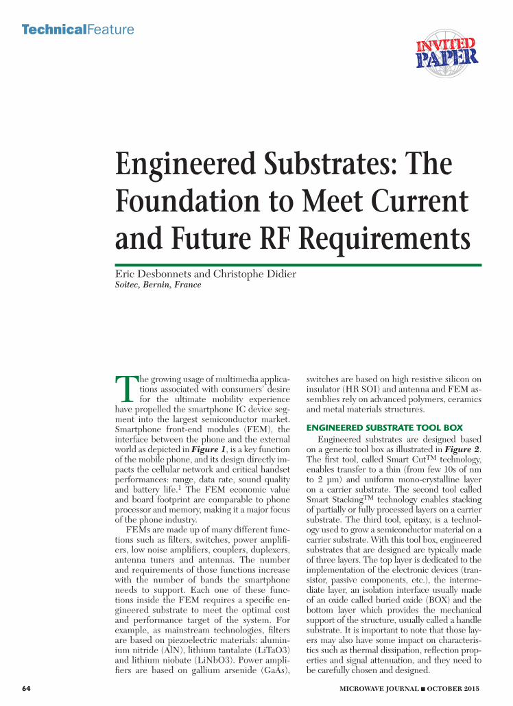
ENGINEERED SUBSTRATE TOOL BOXEngineered substrates are designed based
on a generic tool box as illustrated in Figure 2. The first tool, called Smart CutTM technology, enables transfer to a thin (from few 10s of nm to 2 µm) and uniform mono-crystalline layer on a carrier substrate. The second tool called Smart StackingTM technology enables stacking of partially or fully processed layers on a carrier substrate. The third tool, epitaxy, is a technol-ogy used to grow a semiconductor material on a carrier substrate. With this tool box, engineered substrates that are designed are typically made of three layers. The top layer is dedicated to the implementation of the electronic devices (tran-sistor, passive components, etc.), the interme-diate layer, an isolation interface usually made of an oxide called buried oxide (BOX) and the bottom layer which provides the mechanical support of the structure, usually called a handle substrate. It is important to note that those lay-ers may also have some impact on characteris-tics such as thermal dissipation, reflection prop-erties and signal attenuation, and they need to be carefully chosen and designed.
64 MICROWAVE JOURNAL OCTOBER 2015
TechnicalFeature
_10M28 FINAL.indd 64 9/28/15 2:54 PM

66 MICROWAVE JOURNAL OCTOBER 2015
TechnicalFeature
LINEARITY CHALLENGEAccording to Cisco,2 mobile data
traffi c will grow at a 61 percent CAGR between 2013 and 2018, mainly driv-en by multimedia applications and, in particular, video exchange. The cel-lular roadmap is addressing this data traffi c boom by improving spectral ef-fi ciency, increasing available spectrum and increasing network cell density. Key techniques to increase capacity are carrier aggregation and MIMO (multi-input-multi-output). To be ef-fi cient, those transmission techniques impose additional requirements on the FEM such as higher linearity, as shown in Table 1.
Fig. 1 FEM block diagram.
FilterBank
AntennaSwitch Module
AntennaSwap Switch
AntennaTuner
Coupler
Diplexer
PA ModeSwitch
PowerAmplifier
2G
3GLTE
3GLTE
2G
SupplyModulator
TxHighBand
MODEM
+
TRANSCEIVER
TxLowBand
Rx LowBand
Rx HighBand
MIPI
RxDiversity
Rx DiversitySwitch
TABLE 1LINEARITY REQUIREMENTS PER
CELLULAR GENERATION
Network Linearity (IIP3 in dBm)
2G 55
3G 65
4G LTE 72
4G LTE + CA Up to 90
Source: Intel Mobile, “Challenges For Radios Due To Carrier Aggregation Requirements,” L. Schumacher, Nov. 2012.
Fig. 2 Engineering substrate toolbox.
Thin and UniformMono-CrystallineLayer on CarrierSubstrate
Stacking of (Partially)Processed Layer onCarrier Substrate
Growth ofSemiconductorMaterial
Epitaxy Expertise
Smart StackingTM
Smart CutTM
SiliconStrained SiliconGermaniumIII-V, … SiO2
ONO…
CZ SiliconHigh Resistivity Si
SapphireGlass, …
Device LayerBuried Insulator
Handle Substrate
_10M28 FINAL.indd 66 9/28/15 2:54 PM

68 MICROWAVE JOURNAL OCTOBER 2015
TechnicalFeature
www.WeinschelAssociates.comVisit our new website with interactive catalog and online RFQ!
19212 Orbit DriveGaithersburg, MD 20879Voice: 301.963.4630Fax: [email protected]
• High Power Measurement Systems• Power Amplifier Monitoring• EW Systems Testing
Applications
• High Performance Design• 600 W Average/10kW Peak Power Handling• 0.75 to 12 GHz in Bands• Low Loss Air Dielectric• Operation to +85 C Without Degradation• Multi-Octave Bandwidths
Features NEW!
High Power Couplers
The entire eco-system, from FEM makers, foundries, substrate suppli-ers and research centers, is working together to achieve those linearity re-quirements. Engi-neered substrate providers are trying to provide substrates that will enable bet-ter RF performance and not become the limiting factor for the device. Figure 3 shows the contri-butions to linearity.
RF SOI SUBSTRATESDepending on the architecture
and partitioning of the FEM, device linearity requirements may change drastically from one component to the other. As a rule of thumb, the devices closer to the antenna or the devices on the path of stronger signals will need to exhibit higher linearity. RF SOI is an engineered substrate which comprises a thin film of mono crystal-line silicon fully CMOS compatible as the top layer, an oxide as the isolation layer and a high resistive substrate as the handle substrate. The substrate resistivity can be several k�-cm and should be as high as 10 k�-cm to be considered as RF lossless. As shown in Table 2, RF SOI offers a global de-sign platform for FEMs with several advantages compared to other avail-able options (CMOS compatibility, foundry offering, RF performance, integration and cost effectiveness).
RF SOI includes two different type of substrates: standard high re-sistive SOI (HR SOI) and enhanced signal integrity SOI (RFeSITM SOI). In the RF SOI products, the oxide of the insulator BOX still contains positive charges in the range of a few 10E10 cm2. As demonstrated by Prof. Raskin’s work from Université Catholique of Louvain (UCL), those charges create a parasitic surface con-duction at the interface between the BOX and the high-resistivity handle substrate, typically dropping its resis-tivity by a decade.3,4 To recover the original resistivity of the handle sub-strate, UCL and Soitec have invented
TABLE 2RF-SOI: THE BEST FRONT-END MODULE DEVELOPMENT PLATFORM
Process Figure of Merit RF SOI GaAs SoS Bulk MEMS
CMOS Compatible ++ – – + ++ =
Foundries Capacity Offering ++ + – ++ –
RF Performance (Linearity,...) + ++ + – ++
Full FEM Integration/SoC ++ – + ++ – –
Cost + = – ++ –
s Fig. 3 IC linearity vs. substrate RF performance.
Transition fromsubstrate to IC
main nonlinearitycontributor
Substratelimited
ICLinearity
IClimited
Substrate RFPerformance
TargetSubstrate
s Fig. 4 Types of RF SOI: HR-SOI and RFeSI™ .
RFeSITM
HR-SOI
FixedCharges
Mobile & InterfaceTrapped Charges
UCL &Soitec Patent
Buried Insulating Layer
SiO2 (BOX)High Resistivity SI Base
High Resistivity SI Base
Mono-Crystal Top Silicon
Mono-Crystal Top Silicon
Trap Rich LayerSiO2 (BOX)
_10M28 FINAL.indd 68 9/28/15 2:54 PM

70 MICROWAVE JOURNAL OCTOBER 2015
TechnicalFeature
Clearly extend your dynamic range with our ultra-low-noise, high-linearity, Distributed Ampli�ers.
Clearly extend your dynamic range with our ultra-low-noise,
Wipe out the noise
CustomMMIC.com
for switches with more than 85 per-cent market share in antenna switch modules.8 After a few years of pro-duction of the fi rst generation RFeSI substrate, a second generation (called RFeSI90 substrate) has been introduced this year in order to keep up with in-creasing market lin-earity requirements. As shown in Fig-
ures 5 and 6, RFeSI90 substrates of-fer 10 dB better linearity than RFeSI Gen1 substrates. This makes it suit-able for the most advanced circuits in new LTE-A smartphone applications, while RFeSI Gen1 continues to serve the current market. Improvements have been achieved using a combi-nation of increased handle substrate resistivity as well as a re-engineering of the trap-rich layer. The BOX thick-ness has also been reduced by a fac-tor of two without impacting the RF device performance while improving manufacturability.
RF METROLOGY – HARMONIC QUALITY FACTOR
As shown in Figure 7, there is a gap between the substrate world where we talk about contaminant, oxygen level, dopant, layer thickness and more material-oriented concepts and the RF designer’s world more concerned about RF linearity, losses, power dissipation and IC design-ori-ented concepts. Bridging this gap be-tween the engineered substrate speci-fi cations and the IC linearity specifi ca-tion is a concern for all foundries and RFIC designers when choosing an RF engineered substrate.
Materials engineering and RF en-gineering are two different domains, and specifying the resistivity of the handle substrate using an ohmic sheet resistance measurement at the back-side of the substrate will not guaran-tee the RF performance of the wafer. There are many parameters that can change the RF performance of an RFeSI wafer: the trap-rich layer ma-terial and its characteristics, dopants that can migrate at interfaces between
same design, optimizing the best cost performance trade-off.
UCL and Soitec have widely pub-lished comparisons between bulk Si, HR SOI, RFeSI and quartz sub-strates.5,6,7 As a summary, the RFeSI substrate addresses the critical FEM requirements: higher linearity, re-duced crosstalk, lower insertion loss, better passive device quality factor and, to some extent, higher thermal dissipation. RF SOI substrates have become the mainstream substrate
a method consisting of adding a trap-rich layer on top of the handle wafer that can freeze those carriers as shown in Figure 4. Depending on the linear-ity requirements, designers have then the option to choose one or the other substrate depending on the level of RF performance required for their application; they could even use the
Fig. 5 Second (H2) and third (H3) harmonics measured on RFeSI Gen1 and RFeSI90.
–70
–80
–90
–100
–110
–120
–13025155–5–15–25
Pout
(dB
m)
Pin (dBm)
H2 RFeSI Gen1H3 RFeSI Gen1H2 RFeSI90H3 RFeSI90
Fig. 6 Linearity performance benefi t depends on IC type and RFeSI substrate.
Transition fromsubstrate to IC main
nonlinearitycontributor
IC-BIC-CIC-D
IC Linearity(Circuit Performance)
RFeSI90Performance
Benefit
Substratelimited IC
limited
RFeSI=G1iSubstrate
RFeSI90Substrate
Substrate RFPerformance
_10M28 FINAL.indd 70 9/28/15 2:54 PM

72 MICROWAVE JOURNAL OCTOBER 2015
TechnicalFeature
M I C R O W A V E
AS9100CISO 9001:2008
Space-Qualified Isolators & CirculatorsQuality and delivery are crucial for space applications. Why wait 24+ weeks for delivery from your current supplier? DiTom can deliver Space-Qualified Isolators and Circulators as quickly as 4 weeks depending on your testing needs.
• Engineering and Qualification models are available from L - Ka bands
• In-House 3D and Electromagnetic simulation software
• In-House Environmental Testing Capabilities including
- RF Leakage - Thermal Shock - Temperature Cycling - Random and Sine Vibration - Thermal Vacuum
- RF Leakage- RF Leakage- Thermal Shock- Thermal Shock- Temperature Cycling- Temperature Cycling- Random and Sine Vibration- Random and Sine Vibration- Thermal Vacuum - Thermal Vacuum
www.ditom.com/space(559) 255-7043 | [email protected]
M I C R O W A V E
Space-QualifiedIsolators & CirculatorsIsolators & Circulators
the layers, activation of thermal do-nors during the Smart Cut and found-ry process temperature cycles, doping profi le and thickness of the differ-ent layers, etc. To measure resistivity across the wafer, a technique called spreading resistance profi le (SRP) is commonly used. To quantify the level of linearity of the material, manufac-turers have traditionally measured the level of harmonics generated by a sig-nal injected on a coplanar waveguide (CPW). Soitec has developed a pro-prietary algorithm which integrates the SRP profi le weighted by the depth of the electrical fi eld and matches it to the second harmonic generated through a CPW as shown on Figure 8. This parameter is called harmonic quality factor (HQF) and is included in the RFeSI substrate specifi cations.
BEYOND RF SOI SWITCHESIntegrating more FEM devices is
an on-going challenge for the indus-try. RF SOI is the ideal platform to
Fig. 7 Improving RF performance requires understanding how wafer parameters affect linearity.
Layers thickness
OxygenType
DopantContamination
Linearity (dBm)
Fig. 8 The HQF correlates the SRP with the measured second harmonic.
0 l
CPW
L
900 MHzPin = 15 dBm
Fundamental
Coplanar Waveguide Setup
Spreading Resistance Profile
Harmonics
DepthRes
isti
vity
(�
. cm
)
H2 � HQF �� d�(x)e dx
–X
_10M28 FINAL.indd 72 9/28/15 2:54 PM

74 MICROWAVE JOURNAL OCTOBER 2015
TechnicalFeature
ni-microwavecomponents.com/quicksyn
©2015 National Instruments. All rights reserved. National Instruments, NI, and ni.com are trademarks of National Instruments.
Redefining Frequency Synthesizers
With QuickSyn Technology
408 610 6810
Design smaller and more efficiently with
National Instruments QuickSyn synthesizers. The revolutionary
phase-refining technology used in QuickSyn synthesizers enables
blazing fast switching speeds, very low spurious and phase noise
performance, wide frequency range, and small footprint.
QuickSyn Lite Models
FSL-0010 0.65 to 10 GHz Coverage | 0.001 Hz Resolution | +15 dBm $3950 $3500*
FSL-0020 0.65 to 20 GHz Coverage | 0.001 Hz Resolution | +10 dBM $5950 $5300*
10% Promotionalat a Special
Discount
Now Offered
*Special low pricing applies to all QuickSyn products until end of 2015 and is applicable worldwide.
Some RF SOI foundries have be-gun offering 300 mm diameter wafers. We expect future offerings of process nodes beyond 90 nm that will provide opportunities to address applications beyond the current FEM technology by combining advanced digital pro-cessing and analog SOI advantages: faster frequency operation at the same node compared to bulk silicon, lower supply voltage operation down to 0.4 V, high voltage handling, temperature op-eration much beyond 150°C, very low sensitivity to soft error rate and more. Recent switch technology history has demonstrated that in the high volume, highly competitive consumer electron-ics market, a new technology can very rapidly displace the incumbent tech-nology, GaAs in this case. The engi-neered substrate tool box is extremely powerful, enabling the manufacture of the most adapted substrate for a very dynamic ecosystem ready to adopt new substrates when performance and cost warrants. n
References1. E. Desbonnets, S. Laurent, “RF Subs-
trate Technologies for Mobile Applica-tions,” Soitec White Paper, 2011.
2. Cisco VNI Mobile, February 20143. D. Lederer and J.P. Raskin, “Effective
Resistivity of Fully-Processed SOI Sub-strates,” Solid-State Electronics, Vol. 49, No. 3, 2005, pp. 491�496.
4. D. Lederer and J.P. Raskin, “New Sub-strate Passivation Method Dedicated to HR SOI Wafer Fabrication with In-creased Substrate Resistivity,” IEEE Electron Device Letters, Vol. 26, No. 11, 2005, pp. 805�807.
5. K. Ben Ali, C. Roda Neve, A. Gharsal-lah, and J.P. Raskin, “RF Performance of SOI CMOS Technology on Commercial 200 mm High Resistivity Silicon Trap-Rich Wafers,” IEEE Transactions on Electron Devices, Vol. 61, No. 3, March 2014., pp. 722�728.
6. C. Roda Neve and J.P. Raskin, “RF Har-monic Distortion of CPW Lines on HR-Si and Trap-Rich HR-Si Substrates,” IEEE Transactions on Electron Devices, Vol. 59, 2012, pp. 924�932.
7. Yonghyun Shim, J.P. Raskin, C. Roda Neve and M. Rais-Zadeh, “RF MEMS Passives on High-Resistivity Silicon Sub-strates,” IEEE Microwave and Wireless Components Letters, Vol. 23, No. 12, December 2013, pp. 632�634.
8. Sapphire Applications & Market: from LED to Consumer Electronic, Yole, 2014.
market, chosen by some first adopt-ers like ZTE. Tunable filter solutions partly or fully integrated on RF SOI are in research and development. The competition with current piezo-electric filters, having quality factors of few thousands, is difficult with typ-ical discrete and on-chip inductors that have quality factors of a hundred or less. The first phase is to lower the filter bill of materials by doing part of the filtering on chip.
expand this roadmap. RF SOI is al-ready a mainstream technology for switches used in all different configu-rations (antenna, antenna swapping, power amplifier mode, diversity, antenna tuner). Active components such as LNAs and passive compo-nents such as couplers are also be-ing integrated on a single die with switches. Power amplifiers using RF SOI were launched in the market in 2013 addressing the LTE and LTE-A
_10M28 FINAL.indd 74 9/28/15 2:54 PM