1.25-w mono fully differential audio power amplifier … · symbolization aani aaoi aapi (1) the...
TRANSCRIPT

ZQV DRB DGN
1FEATURES APPLICATIONS
DESCRIPTION
APPLICATION CIRCUIT
Actual Solution Size
6,9 mm
5,25 mm
(1)CB
RI
RI
CS
RF
RF
_
+
VDD
VO+
VO-
GND
To Battery
Cs
Bias
Circuitry
IN-
IN++
-
In From
DAC
SHUTDOWN
RI
RI
RF
RF
Applies to the ZQV Packages Only
C( )BYPASS
(Optional)
TPA6205A1
www.ti.com .............................................................................................................................................................. SLOS490B–JULY 2006–REVISED JUNE 2008
1.25-W MONO FULLY DIFFERENTIAL AUDIO POWER AMPLIFIER WITH 1.8-V INPUTLOGIC THRESHOLDS
• Designed for Wireless Handsets, PDAs, and2• 1.25 W Into 8Ω From a 5-V Supply atother mobile devicesTHD = 1% (Typical)
• Compatible with Low Power (1.8V Logic) I/O• Shutdown Pin has 1.8V CompatibleThreshold control signalsThresholds
• Low Supply Current: 1.7mA Typical• Shutdown Current < 10µA
The TPA6205A1 is a 1.25-W mono fully differential• Only Five External Components amplifier designed to drive a speaker with at least– Improved PSRR (90 dB) and Wide Supply 8-Ω impedance while consuming less than 37 mm2
Voltage (2.5V to 5.5V) for Direct Battery (ZQV package option) total printed-circuit board(PCB) area in most applications. This device operatesOperationfrom 2.5 V to 5.5 V, drawing only 1.7 mA of quiescent– Fully Differential Design Reduces RFsupply current. The TPA6205A1 is available in theRectification space-saving 2 mm x 2 mm MicroStar Junior™ BGA
– Improved CMRR Eliminates Two Input package, and the space saving 3 mm x 3 mm QFNCoupling Capacitors (DRB) package.
– C(BYPASS) Is Optional Due to Fully Features like 85-dB PSRR from 90 Hz to 5 kHz,Differential Design and High PSRR improved RF-rectification immunity, and small PCB
area makes the TPA6205A1 ideal for wireless• Available in 3 mm x 3 mm QFN Package (DRB)handsets. A fast start-up time of 4 µs with minimal• Available in an 8-Pin PowerPAD™ MSOPpop makes the TPA6205A1 ideal for PDA(DGN) applications.
• Avaliable in a 2 mm x 2 mm MicroStar Junior™BGA Package (ZQV)
1
Please be aware that an important notice concerning availability, standard warranty, and use in critical applications of TexasInstruments semiconductor products and disclaimers thereto appears at the end of this data sheet.
2PowerPAD, MicroStar Junior are trademarks of Texas Instruments.
PRODUCTION DATA information is current as of publication date. Copyright © 2006–2008, Texas Instruments IncorporatedProducts conform to specifications per the terms of the TexasInstruments standard warranty. Production processing does notnecessarily include testing of all parameters.

ABSOLUTE MAXIMUM RATINGS
RECOMMENDED OPERATING CONDITIONS
DISSIPATION RATINGS
TPA6205A1
SLOS490B–JULY 2006–REVISED JUNE 2008 .............................................................................................................................................................. www.ti.com
These devices have limited built-in ESD protection. The leads should be shorted together or the device placed in conductive foamduring storage or handling to prevent electrostatic damage to the MOS gates.
ORDERING INFORMATIONPACKAGED DEVICES (1) (2)
MicroStar Junior™ QFN MSOP(ZQV) (DRB) (DGN)
Device TPA6205A1ZQVR TPA6205A1DRB TPA6205A1DGNSymbolization AANI AAOI AAPI
(1) The ZQV packages are only available taped and reeled. The suffix R designates taped and reeled parts.(2) For the most current package and ordering information, see the Package Option Addendum at the end of this document, or see the TI
website at www.ti.com.
over operating free-air temperature range unless otherwise noted (1)
UNITVDD Supply voltage –0.3 V to 6 VVI Input voltage INx and SHUTDOWN pins –0.3 V to VDD + 0.3 V
Continuous total power dissipation See Dissipation Rating TableTA Operating free-air temperature –40°C to 85°CTJ Junction temperature –40°C to 125°CTstg Storage temperature –65°C to 150°C
Lead temperature 1,6 mm (1/16 Inch) ZQV, DRB, DGN 260°Cfrom case for 10 seconds
(1) Stresses beyond those listed under "absolute maximum ratings” may cause permanent damage to the device. These are stress ratingsonly, and functional operation of the device at these or any other conditions beyond those indicated under "recommended operatingconditions” is not implied. Exposure to absolute-maximum-rated conditions for extended periods may affect device reliability.
MIN TYP MAX UNITVDD Supply voltage 2.5 5.5 VVIH High-level input voltage SHUTDOWN 1.15 VVIL Low-level input voltage SHUTDOWN 0.50 VVIC Common-mode input voltage VDD = 2.5 V, 5.5 V, CMRR ≤ –60 dB 0.5 VDD–0.8 VTA Operating free-air temperature –40 85 °CZL Load impedance 6.4 8 Ω
TA ≤ 25°C TA = 70°C TA = 85°CPACKAGE DERATING FACTORPOWER RATING POWER RATING POWER RATINGZQV 885 mW 8.8 mW/°C 486 mW 354 mWDGN 2.13 W 17.1 mW/°C 1.36 W 1.11 WDRB 2.7 W 21.8 mW/°C 1.7 W 1.4 W
2 Submit Documentation Feedback Copyright © 2006–2008, Texas Instruments Incorporated
Product Folder Link(s): TPA6205A1

ELECTRICAL CHARACTERISTICS
OPERATING CHARACTERISTICS
TPA6205A1
www.ti.com .............................................................................................................................................................. SLOS490B–JULY 2006–REVISED JUNE 2008
TA = 25°C, Gain = 1 V/V
PARAMETER TEST CONDITIONS MIN TYP MAX UNITOutput offset voltage (measured|VOO| VI = 0 V, VDD = 2.5 V to 5.5 V 9 mVdifferentially)
PSRR Power supply rejection ratio VDD = 2.5 V to 5.5 V –90 –70 dBVDD = 3.6 V to 5.5 V, VIC = 0.5 V to VDD–0.8 –70 –65
CMRR Common-mode rejection ratio dBVDD = 2.5 V, VIC = 0.5 V to 1.7 V –62 –55
VDD = 5.5 V 0.30 0.46RL = 8 Ω, VIN+ = VDD,VOL Low-level output voltage VDD = 3.6 V 0.22 VVIN– = 0 V or VIN+ = 0 V, VIN– = VDD
VDD = 2.5 V 0.19 0.26VDD = 5.5 V 4.8 5.12
RL = 8 Ω, VIN+ = VDD,VOH High-level output voltage VDD = 3.6 V 3.28 VVIN– = 0 V or VIN+ = 0 V, VIN– = VDDVDD = 2.5 V 2.1 2.24
|IIH| High-level input current VDD = 5.5 V, VI = 5.8 V 1.2 µA|IIL| Low-level input current VDD = 5.5 V, VI = –0.3 V 1.2 µAIDD Supply current VDD = 2.5 V to 5.5 V, No load, SHUTDOWN = VIH 1.7 2 mAIDD(SD) Supply current in shutdown mode SHUTDOWN = VIL , VDD = 2.5 V to 5.5 V, No load 0.01 0.9 µA
TA = 25°C, Gain = 1 V/V, RL = 8 Ω
PARAMETER TEST CONDITIONS MIN TYP MAX UNITVDD = 5 V 1.25
PO Output power THD + N = 1%, f = 1 kHz VDD = 3.6 V 0.63 WVDD = 2.5 V 0.3
VDD = 5 V, PO = 1 W, f = 1 kHz 0.06%Total harmonicTHD+N VDD = 3.6 V, PO = 0.5 W, f = 1 kHz 0.07%distortion plus noise
VDD = 2.5 V, PO = 200 mW, f = 1 kHz 0.08%C(BYPASS) = 0.47°F, VDD = 3.6 V to 5.5 V, f = 217 Hz to 2 kHz, -87Inputs ac-grounded with CI = 2 µF VRIPPLE = 200 mVPP
Supply ripple rejection C(BYPASS) = 0.47 µF, VDD = 2.5 V to 3.6 V, f = 217 Hz to 2 kHz,kSVR -82 dBratio Inputs ac-grounded with CI = 2 µF VRIPPLE = 200 mVPP
C(BYPASS) = 0.47 µF, VDD = 2.5 V to 5.5 V, f = 40 Hz to 20 kHz, ≤–74Inputs ac-grounded with CI = 2 µF VRIPPLE = 200 mVPP
SNR Signal-to-noise ratio VDD = 5 V, PO= 1 W 104 dBNo weighting 17
Vn Output voltage noise f = 20 Hz to 20 kHz µVRMSA weighting 13VDD = 2.5 V to 5.5 V, f = 20 Hz to 1 kHz ≤–85Common-modeCMRR Resistor tolerance = 0.1%, dBrejection ratio f = 20 Hz to 20 kHz ≤–74Gain = 4V/V, VICM = 200 mVPP
ZI Input impedance 2 MΩZO Output impedance Shutdown mode >10k
Shutdown attenuation f = 20 Hz to 20 kHz, RF = RI = 20 kΩ -80 dB
Copyright © 2006–2008, Texas Instruments Incorporated Submit Documentation Feedback 3
Product Folder Link(s): TPA6205A1

(SIDE VIEW)
SHUTDOWN
IN+
VDDVO+
GND
VO-
IN-
AB
C
1 2 3
BYPASS
8SHUTDOWN
BYPASS
IN+
IN-
VO-
GND
VDD
VO+
7
6
5
1
2
3
4
7
6
5
1
2
3
SHUTDOWN
BYPASS
IN+
IN-
VO-
GND
VDD
VO+4
8
TPA6205A1
SLOS490B–JULY 2006–REVISED JUNE 2008 .............................................................................................................................................................. www.ti.com
MicroStar Junior™ (ZQV) PACKAGE(TOP VIEW)
8-PIN QFN (DRB) PACKAGE(TOP VIEW)
8-PIN MSOP (DGN) PACKAGE(TOP VIEW)
Terminal FunctionsTERMINAL
I/O DESCRIPTIONDRB,NAME ZQV DGNBYPASS C1 2 I Mid-supply voltage. Adding a bypass capacitor improves PSRR.GND B2 7 I High-current groundIN- C3 4 I Negative differential inputIN+ C2 3 I Positive differential inputSHUTDOWN B1 1 I Shutdown terminal (active low logic)VDD A3 6 I Supply voltage terminalVO+ B3 5 O Positive BTL outputVO- A1 8 O Negative BTL output
N/A Connect to ground. Thermal pad must be soldered down in all applications to properly secureThermal Pad device on the PCB.
4 Submit Documentation Feedback Copyright © 2006–2008, Texas Instruments Incorporated
Product Folder Link(s): TPA6205A1
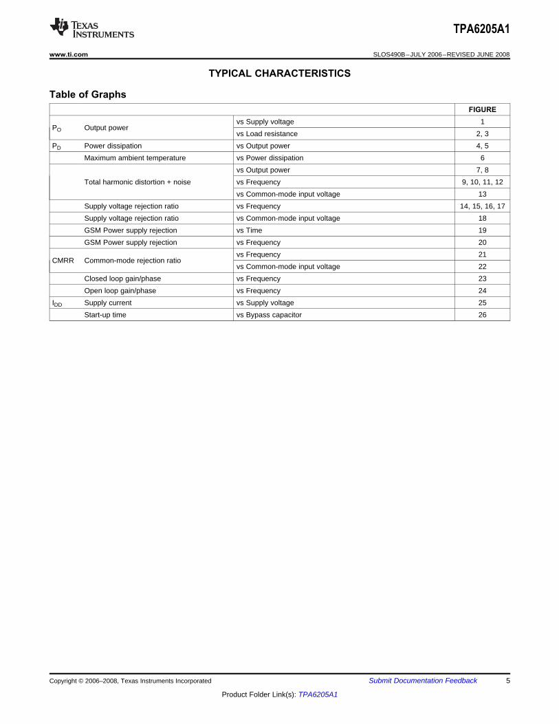
TYPICAL CHARACTERISTICS
Table of Graphs
TPA6205A1
www.ti.com .............................................................................................................................................................. SLOS490B–JULY 2006–REVISED JUNE 2008
FIGUREvs Supply voltage 1
PO Output powervs Load resistance 2, 3
PD Power dissipation vs Output power 4, 5Maximum ambient temperature vs Power dissipation 6
vs Output power 7, 8Total harmonic distortion + noise vs Frequency 9, 10, 11, 12
vs Common-mode input voltage 13Supply voltage rejection ratio vs Frequency 14, 15, 16, 17Supply voltage rejection ratio vs Common-mode input voltage 18GSM Power supply rejection vs Time 19GSM Power supply rejection vs Frequency 20
vs Frequency 21CMRR Common-mode rejection ratio
vs Common-mode input voltage 22Closed loop gain/phase vs Frequency 23Open loop gain/phase vs Frequency 24
IDD Supply current vs Supply voltage 25Start-up time vs Bypass capacitor 26
Copyright © 2006–2008, Texas Instruments Incorporated Submit Documentation Feedback 5
Product Folder Link(s): TPA6205A1

TYPICAL CHARACTERISTICS
0
0.2
0.4
0.6
0.8
1
1.2
1.4
1.6
1.8
8 13 18 23 28
VDD = 5 V
VDD = 3.6 V
VDD = 2.5 V
RL - Load Resistance - Ω
- O
utp
ut
Po
wer
- W
P O
f = 1 kHzTHD+N = 10%Gain = 1 V/V
320
0.2
0.4
0.6
0.8
1
1.2
1.4
1.6
1.8
2.5 3 3.5 4 4.5 5
VDD - Supply Voltage - V
- O
utp
ut
Po
wer
- W
P O
RL = 8 Ωf = 1 kHzGain = 1 V/V
THD+N = 1%
THD+N = 10%
0
0.2
0.4
0.6
0.8
1
1.2
1.4
8 13 18 23 28
VDD = 5 V
VDD = 3.6 V
VDD = 2.5 V
RL - Load Resistance - Ω
- O
utp
ut
Po
wer
- W
P O
f = 1 kHzTHD+N = 1%Gain = 1 V/V
32
0
10
20
30
40
50
60
70
80
90
0 0.1 0.2 0.3 0.4 0.5 0.6 0.7 0.8
PD - Power Dissipation - W
Ma
xim
um
Am
bie
nt
Te
mp
era
ture
-C
o
ZQV Package Only
0
0.05
0.1
0.15
0.2
0.25
0.3
0.35
0.4
0 0.2 0.4 0.6 0.8
8 Ω
16 Ω
PO - Output Power - W
- P
ow
er D
issi
pat
ion
- W
P D
VDD = 3.6 V
0 0.2 0.4 0.6 0.8 1 1.2 1.4
8 Ω
16 Ω
PO - Output Power - W
- P
ow
er D
issi
pat
ion
- W
P D
VDD = 5 V
0
0.1
0.2
0.3
0.4
0.5
0.6
0.7
VDD = 5 VCI = 2 µFRL = 8 ΩC(Bypass) = 0 to 1 µFGain = 1 V/V
0.001
10
0.002
0.005
0.01
0.02
0.05
0.1
0.2
0.5
1
2
5
20 20 k100 200 1 k 2 k 10 kf - Frequency - Hz
TH
D+N
- T
ota
l Har
mo
nic
Dis
tort
ion
+ N
ois
e -
%
50 mW
250 mW
1 W
10
0.01
0.02
0.05
0.1
0.2
0.5
1
2
5
10 m 3100 m 1 2
PO - Output Power - W
TH
D+N
- T
ota
l Har
mo
nic
Dis
tort
ion
+ N
ois
e -
%
2.5 V
3.6 V
5 V
RL = 8 Ω, f = 1 kHzC(Bypass) = 0 to 1 µFGain = 1 V/V
10
0.01
0.02
0.05
0.1
0.2
0.5
1
2
5
10 m 100 m 1 2
PO - Output Power - W
TH
D+N
- T
ota
l Har
mo
nic
Dis
tort
ion
+ N
ois
e -
%
2.5 V 5 V
3.6 V
RL = 16 Ωf = 1 kHzC(Bypass) = 0 to 1 µFGain = 1 V/V
TPA6205A1
SLOS490B–JULY 2006–REVISED JUNE 2008 .............................................................................................................................................................. www.ti.com
OUTPUT POWER OUTPUT POWER OUTPUT POWERvs vs vs
SUPPLY VOLTAGE LOAD RESISTANCE LOAD RESISTANCE
Figure 1. Figure 2. Figure 3.
MAXIMUM AMBIENTPOWER DISSIPATION POWER DISSIPATION TEMPERATURE
vs vs vsOUTPUT POWER OUTPUT POWER POWER DISSIPATION
Figure 4. Figure 5. Figure 6.
TOTAL HARMONIC DISTORTION + TOTAL HARMONIC DISTORTION + TOTAL HARMONIC DISTORTION +NOISE NOISE NOISEvs vs vs
OUTPUT POWER OUTPUT POWER FREQUENCY
Figure 7. Figure 8. Figure 9.
6 Submit Documentation Feedback Copyright © 2006–2008, Texas Instruments Incorporated
Product Folder Link(s): TPA6205A1

0.001
10
0.002
0.005
0.01
0.02
0.05
0.1
0.2
0.5
1
2
5
20 20 k50 100 200 500 1 k 2 k 5 k 10 kf - Frequency - Hz
TH
D+N
- T
ota
l Har
mo
nic
Dis
tort
ion
+ N
ois
e -
%
25 mW
125 mW
500 mW
VDD = 3.6 VCI = 2 µFRL = 8 ΩC(Bypass) = 0 to 1 µFGain = 1 V/V
0.001
10
0.002
0.005
0.01
0.02
0.05
0.1
0.2
0.5
1
2
5
20 20 k50 100 200 500 1 k 2 k 5 k 10 kf - Frequency - Hz
TH
D+N
- T
ota
l Har
mo
nic
Dis
tort
ion
+ N
ois
e -
%
15 mW
200 mW
75 mW
VDD = 2.5 VCI = 2 µFRL = 8 ΩC(Bypass) = 0 to 1 µFGain = 1 V/V
VDD = 3.6 VCI = 2 µFRL = 16 ΩC(Bypass) = 0 to 1 µFGain = 1 V/V
0.001
10
0.002
0.005
0.01
0.02
0.05
0.1
0.2
0.5
1
2
5
20 20 k50 100 200 500 1 k 2 k 5 k 10 kf - Frequency - Hz
TH
D+N
- T
ota
l Har
mo
nic
Dis
tort
ion
+ N
ois
e -
%
25 mW
250 mW
125 mW
-100
0
-90
-80
-70
-60
-50
-40
-30
-20
-10
20 20 k50 100 200 500 1 k 2 k 5 k 10 k
VDD = 3.6 V
VDD = 5 VVDD =2. 5 V
f - Frequency - Hz
- S
up
ply
Vo
ltag
e R
ejec
tio
n R
atio
- d
Bk
SV
R
CI = 2 µFRL = 8 ΩC(Bypass) = 0.47 µFVp-p = 200 mVInputs ac-GroundedGain = 1 V/V
-100
0
-90
-80
-70
-60
-50
-40
-30
-20
-10
20 20 k50 100 200 500 1 k 2 k 5 k 10 k
f - Frequency - Hz
- S
up
ply
Vo
ltag
e R
ejec
tio
n R
atio
- d
Bk
SV
R VDD = 3.6 V
VDD = 5 V
VDD =2. 5 V
Gain = 5 V/VCI = 2 µFRL = 8 ΩC(Bypass) = 0.47 µFVp-p = 200 mVInputs ac-Grounded
0.01
0.10
1
10
0 0.5 1 1.5 2 2.5 3 3.5
VDD = 2.5 V
VDD = 3.6 V
f = 1 kHzPO = 200 mW
VIC - Common Mode Input Voltage - V
TH
D+N
- T
ota
l Har
mo
nic
Dis
tort
ion
+ N
ois
e -
%
-90
-80
-70
-60
-50
-40
-30
-20
-10
0 1 2 3 4 5VIC - Common Mode Input Voltage - V
f = 217 HzC(Bypass) = 0.47 µFRL = 8 ΩGain = 1 V/V
VDD = 2.5 V VDD = 3.6 V
VDD = 5 V
- S
up
ply
Vo
ltag
e R
ejec
tio
n R
atio
- d
Bk S
VR
-100
0
-90
-80
-70
-60
-50
-40
-30
-20
-10
20 20 k50 100 200 500 1 k 2 k 5 k 10 k
f - Frequency - Hz
- S
up
ply
Vo
ltag
e R
ejec
tio
n R
atio
- d
Bk
SV
R
VDD =2. 5 V
VDD = 5 V
VDD = 3.6 V
CI = 2 µFRL = 8 ΩInputs FloatingGain = 1 V/V
VDD = 3.6 VCI = 2 µFRL = 8 ΩInputs ac-GroundedGain = 1 V/V
-100
0
-90
-80
-70
-60
-50
-40
-30
-20
-10
20 20 k50 100 200 500 1 k 2 k 5 k 10 k
f - Frequency - Hz
- S
up
ply
Vo
ltag
e R
ejec
tio
n R
atio
- d
Bk
SV
R
C(Bypass) = 0.1 µF
C(Bypass) = 0C(Bypass) = 0.47 µF
C(Bypass) = 1 µF
TPA6205A1
www.ti.com .............................................................................................................................................................. SLOS490B–JULY 2006–REVISED JUNE 2008
TYPICAL CHARACTERISTICS (continued)
TOTAL HARMONIC DISTORTION + TOTAL HARMONIC DISTORTION + TOTAL HARMONIC DISTORTION +NOISE NOISE NOISEvs vs vs
FREQUENCY FREQUENCY FREQUENCY
Figure 10. Figure 11. Figure 12.
TOTAL HARMONIC DISTORTION + SUPPLY VOLTAGE REJECTION SUPPLY VOLTAGE REJECTIONNOISE RATIO RATIOvs vs vs
COMMON MODE INPUT VOLTAGE FREQUENCY FREQUENCY
Figure 13. Figure 14. Figure 15.
SUPPLY VOLTAGE REJECTION SUPPLY VOLTAGE REJECTION SUPPLY VOLTAGE REJECTIONRATIO RATIO RATIOvs vs vs
FREQUENCY FREQUENCY COMMON MODE INPUT VOLTAGE
Figure 16. Figure 17. Figure 18.
Copyright © 2006–2008, Texas Instruments Incorporated Submit Documentation Feedback 7
Product Folder Link(s): TPA6205A1

f - Frequency - Hz
0
-50
-100
0 200 400 600 800 1k 1.2k
- O
utp
ut
Volt
age
- d
BV
1.4k1.6k1.8k 2k-150
-150
-100
0
-50
V O
- S
up
ply
Vo
ltag
e -
dB
VV
DD
VDD Shown in Figure 19CI = 2 µF,C(Bypass) = 0.47 µF,Inputs ac-GroundedGain = 1V/V
C1Frequency217.41 Hz
C1 - Duty20 %
C1 High3.598 V
C1 Pk-Pk504 mV
Vo
ltag
e -
V
Ch1 100 mV/divCh4 10 mV/div
2 ms/div
t - Time - ms
VDD
VO
-100
0
-90
-80
-70
-60
-50
-40
-30
-20
-10
20 20 k50 100 200 500 1 k 2 k 5 k 10 k
f - Frequency - Hz
CM
RR
- C
om
mo
n M
od
e R
ejec
tio
n R
atio
- d
B
VDD = 2.5 V to 5 VVIC = 200 mVp-pRL = 8 ΩGain = 1 V/V
-70
-60
-50
-40
-30
-20
-10
0
10
20
30
40
10 100 10 k 100 k 1 M 10 M-220
-180
-140
-100
-60
-20
20
60
100
140
180
220
1 k
f - Frequency - Hz
Gai
n -
dB
Ph
ase
- D
egre
es
Gain
Phase
VDD = 3.6 VRL = 8 ΩGain = 1 V/V
-200
-150
-100
-50
0
50
100
150
200
100 1 k 10 k 100 k 1 M-200
-150
-100
-50
0
50
100
150
200
f - Frequency - Hz
Gai
n -
dB
Ph
ase
- D
egre
es
Gain
Phase
VDD = 3.6 VRL = 8 Ω
10 M-100
-90
-80
-70
-60
-50
-40
-30
-20
-10
0
0 0.5 1 1.5 2 2.5 3 3.5 4 4.5 5
RL = 8 ΩGain = 1 V/V
VIC - Common Mode Input Voltage - V
CM
RR
- C
om
mo
n M
od
e R
ejec
tio
n R
atio
- d
B
VDD = 3.6 V
VDD = 5 V
VDD = 2.5 V
0
0.2
0.4
0.6
0.8
1
1.2
1.4
1.6
1.8
0 0.5 1 1.5 2 2.5 3 3.5 4 4.5 5 5.5
VDD - Supply Voltage - V
- S
up
ply
Cu
rren
t -
mA
I DD
0
1
2
3
4
5
6
0 0.5 1 1.5 2C(Bypass) - Bypass Capacitor - µF
Sta
rt-U
p T
ime
- m
s
(1) Start-Up time is the time it takes (from alow-to-high transition on SHUTDOWN) for thegain of the amplifier to reach -3 dB of the finalgain.
TPA6205A1
SLOS490B–JULY 2006–REVISED JUNE 2008 .............................................................................................................................................................. www.ti.com
TYPICAL CHARACTERISTICS (continued)
GSM POWER SUPPLY GSM POWER SUPPLYREJECTION REJECTION COMMON MODE REJECTION RATIO
vs vs vsTIME FREQUENCY FREQUENCY
Figure 19. Figure 20. Figure 21.
COMMON MODE REJECTION RATIO CLOSED LOOP GAIN/PHASE OPEN LOOP GAIN/PHASEvs vs vs
COMMON MODE INPUT VOLTAGE FREQUENCY FREQUENCY
Figure 22. Figure 23. Figure 24.
SUPPLY CURRENT START-UP TIME(1)vs vs
SUPPLY VOLTAGE BYPASS CAPACITOR
Figure 25. Figure 26.
8 Submit Documentation Feedback Copyright © 2006–2008, Texas Instruments Incorporated
Product Folder Link(s): TPA6205A1

APPLICATION INFORMATION
FULLY DIFFERENTIAL AMPLIFIER
APPLICATION SCHEMATICSAdvantages of Fully Differential Amplifiers
_
+
VDD
VO+
VO-
GND
To Battery
Cs
Bias
Circuitry
IN-
IN++
-
In From
DAC
SHUTDOWN
RI
RI
C( )BYPASS
(Optional)
RF
RF
TPA6205A1
www.ti.com .............................................................................................................................................................. SLOS490B–JULY 2006–REVISED JUNE 2008
negative channels equally and cancels at thedifferential output. However, removing the bypasscapacitor slightly worsens power supply rejection
The TPA6205A1 is a fully differential amplifier with ratio (kSVR), but a slight decrease of kSVR may bedifferential inputs and outputs. The fully differential acceptable when an additional component can beamplifier consists of a differential amplifier and a eliminated (see Figure 17).common- mode amplifier. The differential amplifier • Better RF-immunity: GSM handsets save powerensures that the amplifier outputs a differential by turning on and shutting off the RF transmitter atvoltage that is equal to the differential input times the a rate of 217 Hz. The transmitted signal isgain. The common-mode feedback ensures that the picked-up on input and output traces. The fullycommon-mode voltage at the output is biased around differential amplifier cancels the signal muchVDD/2 regardless of the common- mode voltage at the better than the typical audio amplifier.input.
• Input coupling capacitors not required: A fully Figure 27 through Figure 31 show applicationdifferential amplifier with good CMRR, like the schematics for differential and single-ended inputs.TPA6205A1, allows the inputs to be biased at Typical values are shown in Table 1.voltage other than mid-supply. For example, if aDAC has mid-supply lower than the mid-supply of Table 1. Typical Component Valuesthe TPA6205A1, the common-mode feedback COMPONENT VALUEcircuit adjusts for that, and the TPA6205A1
RI 10 kΩoutputs are still biased at mid-supply of theRF 10 kΩTPA6205A1. The inputs of the TPA6205A1 can
be biased from 0.5 V to VDD - 0.8 V. If the inputs C(BYPASS)(1) 0.22 µF
are biased outside of that range, input coupling CS 1 µFcapacitors are required. CI 0.22 µF
• Mid-supply bypass capacitor, C(BYPASS), not (1) C(BYPASS) is optionalrequired: The fully differential amplifier does notrequire a bypass capacitor. This is because anyshift in the mid-supply affects both positive and
Figure 27. Typical Differential Input Application Schematic
Copyright © 2006–2008, Texas Instruments Incorporated Submit Documentation Feedback 9
Product Folder Link(s): TPA6205A1

_
+
VDD
VO+
VO-
GND
To Battery
Cs
Bias
Circuitry
IN-
IN++
-
IN
SHUTDOWN
RI
RI
RF
RF
CI
CI
C( )BYPASS
(Optional)
_
+
VDD
VO+
VO-
GND
To Battery
Cs
Bias
Circuitry
IN-
IN+
IN
SHUTDOWN
RI
RF
CI
CI
RI
RF
C( )BYPASS
(Optional)
_
+
GND
Bias
Circuitry
IN-
IN++
-
SHUTDOWN
RI1
RI1
RF
RF
C( )BYPASS
(Optional)
To BatteryVDD
VO+
VO-
CS
CI1
CI1
RI2
RI2CI2
CI2
+
-Differential
Input 2
DifferentialInput 1
TPA6205A1
SLOS490B–JULY 2006–REVISED JUNE 2008 .............................................................................................................................................................. www.ti.com
Figure 28. Differential Input Application Schematic Optimized With Input Capacitors
Figure 29. Single-Ended Input Application Schematic
Figure 30. Application Schematic With TPA6205A1 Summing Two Differential Inputs
10 Submit Documentation Feedback Copyright © 2006–2008, Texas Instruments Incorporated
Product Folder Link(s): TPA6205A1

_
+
VDD
VO+
VO-
GND
To Battery
Cs
Bias
Circuitry
IN-
IN+
SHUTDOWN
RI1
RF
CI1
CP
RP
RF
C( )BYPASS
(Optional)
CI2 RI2
Single EndedInput 1
Single EndedInput 2
Input Capacitor (CI)SELECTING COMPONENTS
Resistors (RF and RI)
Gain − RF/RI (1)
fc 1
2RICI (2)
Bypass Capacitor (CBYPASS) and Start-Up Time
–3 dB
fc
CI 1
2RIfc (3)
TPA6205A1
www.ti.com .............................................................................................................................................................. SLOS490B–JULY 2006–REVISED JUNE 2008
Figure 31. Application Schematic With TPA6205A1 Summing Two Single-Ended Inputs
The TPA6205A1 does not require input couplingcapacitors if using a differential input source that isbiased from 0.5 V to VDD - 0.8 V. Use 1% toleranceThe input (RI) and feedback resistors (RF) set theor better gain-setting resistors if not using inputgain of the amplifier according to Equation 1.coupling capacitors.
In the single-ended input application an inputRF and RI should range from 1 kΩ to 100 kΩ. Most capacitor, CI, is required to allow the amplifier to biasgraphs were taken with RF = RI = 20 kΩ. the input signal to the proper dc level. In this case, CI
and RI form a high-pass filter with the cornerResistor matching is very important in fully differentialfrequency determined in Equation 2.amplifiers. The balance of the output on the reference
voltage depends on matched ratios of the resistors.CMRR, PSRR, and the cancellation of the secondharmonic distortion diminishes if resistor mismatchoccurs. Therefore, it is recommended to use 1%tolerance resistors or better to keep the performanceoptimized.
The internal voltage divider at the BYPASS pin of thisdevice sets a mid-supply voltage for internalreferences and sets the output common modevoltage to VDD/2. Adding a capacitor to this pin filtersany noise into this pin and increases the kSVR.C(BYPASS)also determines the rise time of VO+ and VO-when the device is taken out of shutdown. The largerthe capacitor, the slower the rise time. Although the The value of CI is important to consider as it directlyoutput rise time depends on the bypass capacitor affects the bass (low frequency) performance of thevalue, the device passes audio 4 µs after taken out of circuit. Consider the example where RI is 10 kΩ andshutdown and the gain is slowly ramped up based on the specification calls for a flat bass response downC(BYPASS). to 100 Hz. Equation 2 is reconfigured as Equation 3.To minimize pops and clicks, design the circuit so theimpedance (resistance and capacitance) detected byboth inputs, IN+ and IN-, is equal.
In this example, CI is 0.16 µF, so one would likelychoose a value in the range of 0.22 µF to 0.47 µF. Afurther consideration for this capacitor is the leakagepath from the input source through the input network
Copyright © 2006–2008, Texas Instruments Incorporated Submit Documentation Feedback 11
Product Folder Link(s): TPA6205A1

Summing a Differential Input Signal and a
Decoupling Capacitor (CS) Gain 1 VOVI1
RFRI1VV
(6)
Gain 2 VOVI2
RFRI2VV
(7)
USING LOW-ESR CAPACITORS
SUMMING INPUT SIGNALS WITH THE
DIFFERENTIAL OUTPUT VERSUS
Summing Two Differential Input Signals
Gain 1 VOVI1
RFRI1VV
(4)
Gain 2 VOVI2
RFRI2VV
(5)
TPA6205A1
SLOS490B–JULY 2006–REVISED JUNE 2008 .............................................................................................................................................................. www.ti.com
(RI, CI) and the feedback resistor (RF) to the load.Single-Ended Input SignalThis leakage current creates a dc offset voltage at the
input to the amplifier that reduces useful headroom, Figure 31 shows how to sum a differential input signalespecially in high gain applications. For this reason, a and a single-ended input signal. Ground noise canceramic capacitor is the best choice. When polarized couple in through IN+ with this method. It is better tocapacitors are used, the positive side of the capacitor use differential inputs. To assure that each input isshould face the amplifier input in most applications, balanced, the single-ended input must be driven by aas the dc level there is held at VDD/2, which is likely low-impedance source even if the input is not in use.higher than the source dc level. It is important to Both input nodes must see the same impedance forconfirm the capacitor polarity in the application. optimum performance, thus the use of RP and CP.
The TPA6205A1 is a high-performance CMOS audioamplifier that requires adequate power supplydecoupling to ensure the output total harmonicdistortion (THD) is as low as possible. Power supplydecoupling also prevents oscillations for long lead Wherelengths between the amplifier and the speaker. For
CP = CI1 // CI2higher frequency transients, spikes, or digital hash onRP = RI1 // RI2the line, a good low equivalent-series- resistance
(ESR) ceramic capacitor, typically 0.1 µF to 1 µF,placed as close as possible to the device VDD leadworks best. For filtering lower frequency noise
Low-ESR capacitors are recommended throughoutsignals, a 10-µF or greater capacitor placed near thethis applications section. A real (as opposed to ideal)audio power amplifier also helps, but is not requiredcapacitor can be modeled simply as a resistor inin most applications because of the high PSRR of thisseries with an ideal capacitor. The voltage dropdevice.across this resistor minimizes the beneficial effects ofthe capacitor in the circuit. The lower the equivalentvalue of this resistance the more the real capacitorTPA6205A1 behaves like an ideal capacitor.
Most wireless phones or PDAs need to sum signalsat the audio power amplifier or just have two signalsources that need separate gain. The TPA6205A1 SINGLE-ENDED OUTPUTmakes it easy to sum signals or use separate signal
Figure 32 shows a Class-AB audio power amplifiersources with different gains. Many phones now use(APA) in a fully differential configuration. Thethe same speaker for the earpiece and ringer, whereTPA6205A1 amplifier has differential outputs drivingthe wireless phone would require a much lower gainboth ends of the load. There are several potentialfor the phone earpiece than for the ringer. PDAs andbenefits to this differential drive configuration, butphones that have stereo headphones requireinitially consider power to the load. The differentialsumming of the right and left channels to output thedrive to the speaker means that as one side isstereo signal to the mono speaker.slewing up, the other side is slewing down, and viceversa. This in effect doubles the voltage swing on theload as compared to a ground referenced load.
Two extra resistors are needed for summing Plugging 2 × VO(PP) into the power equation, wheredifferential signals (a total of 10 components). The voltage is squared, yields 4× the output power fromgain for each input source can be set independently the same supply rail and load impedance (see(see Equation 4 and Equation 5, and Figure 30). Equation 8).
12 Submit Documentation Feedback Copyright © 2006–2008, Texas Instruments Incorporated
Product Folder Link(s): TPA6205A1

V(rms) VO(PP)
2 2
Power V(rms)
2
RL (8)
RL
CCVO(PP)
VO(PP)
VDD
–3 dB
fc
RL 2x VO(PP)
VO(PP)
–VO(PP)
VDD
VDD
FULLY DIFFERENTIAL AMPLIFIER
fc 1
2RLCC (9)
TPA6205A1
www.ti.com .............................................................................................................................................................. SLOS490B–JULY 2006–REVISED JUNE 2008
eliminates the need for the blocking capacitors.Low-frequency performance is then limited only bythe input network and speaker response. Cost andPCB space are also minimized by eliminating thebulky coupling capacitor.
Figure 33. Single-Ended Output and FrequencyFigure 32. Differential Output Configuration Response
In a typical wireless handset operating at 3.6 V, Increasing power to the load does carry a penalty ofbridging raises the power into an 8-Ω speaker from a increased internal power dissipation. The increasedsingled-ended (SE, ground reference) limit of 200 dissipation is understandable considering that themW to 800 mW. In sound power that is a 6-dB BTL configuration produces 4× the output power ofimprovement—which is loudness that can be heard. the SE configuration.In addition to increased power there are frequencyresponse concerns. Consider the single-supply SEconfiguration shown in Figure 33. A coupling EFFICIENCY AND THERMAL INFORMATIONcapacitor is required to block the dc offset voltagefrom reaching the load. This capacitor can be quite Class-AB amplifiers are inefficient. The primary causelarge (approximately 33 µF to 1000 µF) so it tends to of these inefficiencies is voltage drop across thebe expensive, heavy, occupy valuable PCB area, and output stage transistors. There are two componentshave the additional drawback of limiting of the internal voltage drop. One is the headroom orlow-frequency performance of the system. This dc voltage drop that varies inversely to output power.frequency-limiting effect is due to the high pass filter The second component is due to the sinewave naturenetwork created with the speaker impedance and the of the output. The total voltage drop can becoupling capacitance and is calculated with calculated by subtracting the RMS value of the outputEquation 9. voltage from VDD. The internal voltage drop multiplied
by the average value of the supply current, IDD(avg),determines the internal power dissipation of theamplifier.
For example, a 68-µF capacitor with an 8-Ω speakerwould attenuate low frequencies below 293 Hz. TheBTL configuration cancels the dc offsets, which
Copyright © 2006–2008, Texas Instruments Incorporated Submit Documentation Feedback 13
Product Folder Link(s): TPA6205A1
V(LRMS)
VO
IDD
IDD(avg)
Efficiency of a BTL amplifier PL
PSUP
where:
PL VLrms2
RL, and VLRMS
VP2
, therefore, PL VP
2
2RL
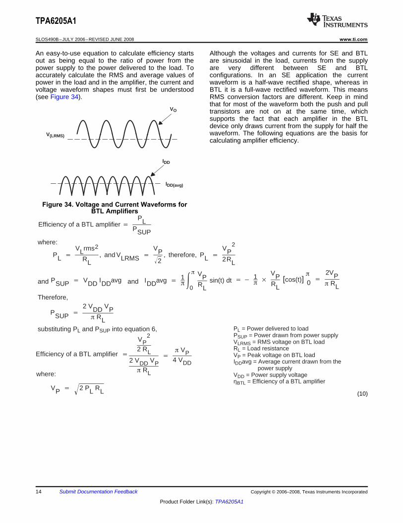
PL = Power delivered to loadPSUP = Power drawn from power supplyVLRMS = RMS voltage on BTL loadRL = Load resistanceVP = Peak voltage on BTL loadIDDavg = Average current drawn from the power supplyVDD = Power supply voltageηBTL = Efficiency of a BTL amplifier
and PSUP VDD IDDavg and IDDavg 1
0
VPRL
sin(t) dt 1
VPRL
[cos(t)]
0 2VP RL
Therefore,
PSUP 2 VDD VP
RLsubstituting PL and PSUP into equation 6,
Efficiency of a BTL amplifier
VP2
2 RL2 VDD VP
RL
VP
4 VDD
VP 2 PL RLwhere:
(10)
TPA6205A1
SLOS490B–JULY 2006–REVISED JUNE 2008 .............................................................................................................................................................. www.ti.com
An easy-to-use equation to calculate efficiency starts Although the voltages and currents for SE and BTLout as being equal to the ratio of power from the are sinusoidal in the load, currents from the supplypower supply to the power delivered to the load. To are very different between SE and BTLaccurately calculate the RMS and average values of configurations. In an SE application the currentpower in the load and in the amplifier, the current and waveform is a half-wave rectified shape, whereas involtage waveform shapes must first be understood BTL it is a full-wave rectified waveform. This means(see Figure 34). RMS conversion factors are different. Keep in mind
that for most of the waveform both the push and pulltransistors are not on at the same time, whichsupports the fact that each amplifier in the BTLdevice only draws current from the supply for half thewaveform. The following equations are the basis forcalculating amplifier efficiency.
Figure 34. Voltage and Current Waveforms forBTL Amplifiers
14 Submit Documentation Feedback Copyright © 2006–2008, Texas Instruments Incorporated
Product Folder Link(s): TPA6205A1

BTL 2 PL RL
4 VDD
Therefore,
(11)TA Max TJ Max ΘJA PDmax
125 113(0.634) 53.3°C (14)
PCB LAYOUT
PD max 2 V2
DD
2RL (12)
ΘJA 1Derating Factor
10.0088
113°CW(13)
TPA6205A1
www.ti.com .............................................................................................................................................................. SLOS490B–JULY 2006–REVISED JUNE 2008
temperature, and the maximum internal dissipation,the maximum ambient temperature can be calculatedwith the following equation. The maximumrecommended junction temperature for theTPA6205A1 is 125°C.
Table 2. Efficiency and Maximum AmbientTemperature vs Output Power in 5-V 8-Ω BTL
SystemsEquation 14 shows that the maximum ambientPower MaxOutput Internal temperature is 53.3°C at maximum power dissipationEfficiency From AmbientPower Dissipation with a 5-V supply.(%) Supply Temperature(W) (W) (W) (°C)Table 2 shows that for most applications no airflow is
0.25 31.4 0.55 0.75 62 required to keep junction temperatures in the0.50 44.4 0.62 1.12 54 specified range. The TPA6205A1 is designed with1.00 62.8 0.59 1.59 58 thermal protection that turns the device off when the
junction temperature surpasses 150°C to prevent1.25 70.2 0.53 1.78 65damage to the IC. Also, using more resistive than 8-Ω
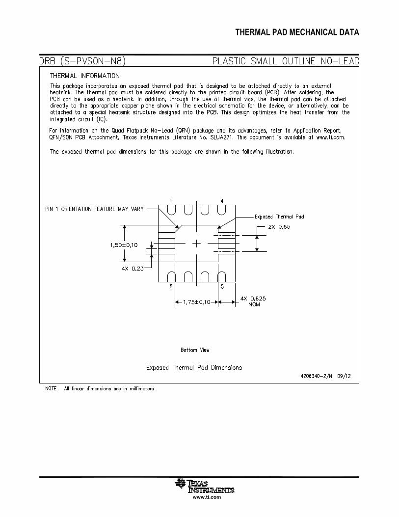
Table 2 employs Equation 11 to calculate efficiencies speakers dramatically increases the thermalfor four different output power levels. Note that the performance by reducing the output current.efficiency of the amplifier is quite low for lower powerlevels and rises sharply as power to the load isincreased resulting in a nearly flat internal power
For the DRB (QFN/SON) and DGN (MSOP)dissipation over the normal operating range. Note thatpackages, it is good practice to minimize thethe internal dissipation at full output power is lesspresence of voids within the exposed thermal padthan in the half power range. Calculating theinterconnection. Total elimination is difficult, but theefficiency for a specific system is the key to properdesign of the exposed pad stencil is key. The stencilpower supply design. For a 1.25-W audio system withdesign proposed in the Texas Instruments application8-Ω loads and a 5-V supply, the maximum draw onnote "QFN/SON PCB Attachment" (SLUA271)the power supply is almost 1.8 W.enables out-gassing of the solder paste during reflow
A final point to remember about Class-AB amplifiers as well as regulating the finished solder thickness.is how to manipulate the terms in the efficiency Typically the solder paste coverage is approximatelyequation to the utmost advantage when possible. 50% of the pad area.Note that in Equation 11, VDD is in the denominator.
In making the pad size for the BGA balls, it isThis indicates that as VDD goes down, efficiency goesrecommended that the layout use solder-up.mask-defined (SMD) land. With this method, the
A simple formula for calculating the maximum power copper pad is made larger than the desired land area,dissipated, PDmax, may be used for a differential and the opening size is defined by the opening in theoutput application: solder mask material. The advantages normally
associated with this technique include more closelycontrolled size and better copper adhesion to thelaminate. Increased copper also increases thethermal performance of the IC. Better size control is
PDmax for a 5-V, 8-Ω system is 634 mW. the result of photo imaging the stencils for masks.Small plated vias should be placed near the centerThe maximum ambient temperature depends on the ball connecting ball B2 to the ground plane. Addedheat sinking ability of the PCB system. The derating plated vias and ground plane act as a heatsink andfactor for the 2 mm x 2 mm Microstar Junior™ increase the thermal performance of the device.package is shown in the dissipation rating table. Figure 35 shows the appropriate diameters for a 2Converting this to θJA: mm × 2 mm MicroStar Junior™ BGA layout.
It is very important to keep the TPA6205A1 externalcomponents very close to the TPA6205A1 to limit
Given θJA, the maximum allowable junction noise pickup. The TPA6205A1 evaluation module(EVM) layout is shown in the next section as a layoutexample.
Copyright © 2006–2008, Texas Instruments Incorporated Submit Documentation Feedback 15
Product Folder Link(s): TPA6205A1

C1
C2
C3
B1
B3
A1
A3
0.25 mm 0.28 mm
0.38 mm
Solder Mask
Paste Mask (Stencil)
Copper Trace
B2 VIAS to Ground Plane
TPA6205A1
SLOS490B–JULY 2006–REVISED JUNE 2008 .............................................................................................................................................................. www.ti.com
Figure 35. MicroStar Junior™ BGA Recommended Layout
16 Submit Documentation Feedback Copyright © 2006–2008, Texas Instruments Incorporated
Product Folder Link(s): TPA6205A1

PACKAGE OPTION ADDENDUM
www.ti.com 24-Jan-2013
Addendum-Page 1
PACKAGING INFORMATION
Orderable Device Status(1)
Package Type PackageDrawing
Pins Package Qty Eco Plan(2)
Lead/Ball Finish MSL Peak Temp(3)
Op Temp (°C) Top-Side Markings(4)
Samples
TPA6205A1DGN ACTIVE MSOP-PowerPAD
DGN 8 80 Green (RoHS& no Sb/Br)
CU NIPDAU Level-1-260C-UNLIM -40 to 85 AAPI
TPA6205A1DGNG4 ACTIVE MSOP-PowerPAD
DGN 8 80 Green (RoHS& no Sb/Br)
CU NIPDAU Level-1-260C-UNLIM -40 to 85 AAPI
TPA6205A1DGNR ACTIVE MSOP-PowerPAD
DGN 8 2500 Green (RoHS& no Sb/Br)
CU NIPDAU Level-1-260C-UNLIM -40 to 85 AAPI
TPA6205A1DGNRG4 ACTIVE MSOP-PowerPAD
DGN 8 2500 Green (RoHS& no Sb/Br)
CU NIPDAU Level-1-260C-UNLIM -40 to 85 AAPI
TPA6205A1DRBR ACTIVE SON DRB 8 3000 Green (RoHS& no Sb/Br)
CU NIPDAU Level-2-260C-1 YEAR -40 to 85 AAOI
TPA6205A1DRBRG4 ACTIVE SON DRB 8 3000 Green (RoHS& no Sb/Br)
CU NIPDAU Level-2-260C-1 YEAR -40 to 85 AAOI
TPA6205A1DRBT ACTIVE SON DRB 8 250 Green (RoHS& no Sb/Br)
CU NIPDAU Level-2-260C-1 YEAR -40 to 85 AAOI
TPA6205A1DRBTG4 ACTIVE SON DRB 8 250 Green (RoHS& no Sb/Br)
CU NIPDAU Level-2-260C-1 YEAR -40 to 85 AAOI
TPA6205A1ZQVR ACTIVE BGAMICROSTAR
JUNIOR
ZQV 8 2500 Green (RoHS& no Sb/Br)
SNAGCU Level-2-260C-1 YEAR -40 to 85 AANI
TPA6205A1ZQVRG1 ACTIVE BGAMICROSTAR
JUNIOR
ZQV 8 2500 Green (RoHS& no Sb/Br)
SNAGCU Level-2-260C-1 YEAR -40 to 85 AANI
(1) The marketing status values are defined as follows:ACTIVE: Product device recommended for new designs.LIFEBUY: TI has announced that the device will be discontinued, and a lifetime-buy period is in effect.NRND: Not recommended for new designs. Device is in production to support existing customers, but TI does not recommend using this part in a new design.PREVIEW: Device has been announced but is not in production. Samples may or may not be available.OBSOLETE: TI has discontinued the production of the device.
(2) Eco Plan - The planned eco-friendly classification: Pb-Free (RoHS), Pb-Free (RoHS Exempt), or Green (RoHS & no Sb/Br) - please check http://www.ti.com/productcontent for the latest availabilityinformation and additional product content details.TBD: The Pb-Free/Green conversion plan has not been defined.Pb-Free (RoHS): TI's terms "Lead-Free" or "Pb-Free" mean semiconductor products that are compatible with the current RoHS requirements for all 6 substances, including the requirement thatlead not exceed 0.1% by weight in homogeneous materials. Where designed to be soldered at high temperatures, TI Pb-Free products are suitable for use in specified lead-free processes.

PACKAGE OPTION ADDENDUM
www.ti.com 24-Jan-2013
Addendum-Page 2
Pb-Free (RoHS Exempt): This component has a RoHS exemption for either 1) lead-based flip-chip solder bumps used between the die and package, or 2) lead-based die adhesive used betweenthe die and leadframe. The component is otherwise considered Pb-Free (RoHS compatible) as defined above.Green (RoHS & no Sb/Br): TI defines "Green" to mean Pb-Free (RoHS compatible), and free of Bromine (Br) and Antimony (Sb) based flame retardants (Br or Sb do not exceed 0.1% by weightin homogeneous material)
(3) MSL, Peak Temp. -- The Moisture Sensitivity Level rating according to the JEDEC industry standard classifications, and peak solder temperature.
(4) Only one of markings shown within the brackets will appear on the physical device.
Important Information and Disclaimer:The information provided on this page represents TI's knowledge and belief as of the date that it is provided. TI bases its knowledge and belief on informationprovided by third parties, and makes no representation or warranty as to the accuracy of such information. Efforts are underway to better integrate information from third parties. TI has taken andcontinues to take reasonable steps to provide representative and accurate information but may not have conducted destructive testing or chemical analysis on incoming materials and chemicals.TI and TI suppliers consider certain information to be proprietary, and thus CAS numbers and other limited information may not be available for release.
In no event shall TI's liability arising out of such information exceed the total purchase price of the TI part(s) at issue in this document sold by TI to Customer on an annual basis.

TAPE AND REEL INFORMATION
*All dimensions are nominal
Device PackageType
PackageDrawing
Pins SPQ ReelDiameter
(mm)
ReelWidth
W1 (mm)
A0(mm)
B0(mm)
K0(mm)
P1(mm)
W(mm)
Pin1Quadrant
TPA6205A1DGNR MSOP-Power PAD
DGN 8 2500 330.0 12.4 5.3 3.4 1.4 8.0 12.0 Q1
TPA6205A1DGNR MSOP-Power PAD
DGN 8 2500 330.0 12.4 5.3 3.4 1.4 8.0 12.0 Q1
TPA6205A1DRBR SON DRB 8 3000 330.0 12.4 3.3 3.3 1.1 8.0 12.0 Q2
TPA6205A1DRBT SON DRB 8 250 180.0 12.4 3.3 3.3 1.1 8.0 12.0 Q2
TPA6205A1ZQVR BGA MI CROSTA
R JUNI OR
ZQV 8 2500 330.0 8.4 2.3 2.3 1.4 4.0 8.0 Q1
TPA6205A1ZQVR BGA MI CROSTA
R JUNI OR
ZQV 8 2500 330.0 8.4 2.3 2.3 1.4 4.0 8.0 Q1
TPA6205A1ZQVRG1 BGA MI CROSTA
R JUNI OR
ZQV 8 2500 330.0 8.4 2.3 2.3 1.4 4.0 8.0 Q1
PACKAGE MATERIALS INFORMATION
www.ti.com 8-Apr-2013
Pack Materials-Page 1

*All dimensions are nominal
Device Package Type Package Drawing Pins SPQ Length (mm) Width (mm) Height (mm)
TPA6205A1DGNR MSOP-PowerPAD DGN 8 2500 358.0 335.0 35.0
TPA6205A1DGNR MSOP-PowerPAD DGN 8 2500 364.0 364.0 27.0
TPA6205A1DRBR SON DRB 8 3000 367.0 367.0 35.0
TPA6205A1DRBT SON DRB 8 250 210.0 185.0 35.0
TPA6205A1ZQVR BGA MICROSTARJUNIOR
ZQV 8 2500 338.1 338.1 20.6
TPA6205A1ZQVR BGA MICROSTARJUNIOR
ZQV 8 2500 338.1 338.1 20.6
TPA6205A1ZQVRG1 BGA MICROSTARJUNIOR
ZQV 8 2500 338.1 338.1 20.6
PACKAGE MATERIALS INFORMATION
www.ti.com 8-Apr-2013
Pack Materials-Page 2


IMPORTANT NOTICE
Texas Instruments Incorporated and its subsidiaries (TI) reserve the right to make corrections, enhancements, improvements and otherchanges to its semiconductor products and services per JESD46, latest issue, and to discontinue any product or service per JESD48, latestissue. Buyers should obtain the latest relevant information before placing orders and should verify that such information is current andcomplete. All semiconductor products (also referred to herein as “components”) are sold subject to TI’s terms and conditions of salesupplied at the time of order acknowledgment.
TI warrants performance of its components to the specifications applicable at the time of sale, in accordance with the warranty in TI’s termsand conditions of sale of semiconductor products. Testing and other quality control techniques are used to the extent TI deems necessaryto support this warranty. Except where mandated by applicable law, testing of all parameters of each component is not necessarilyperformed.
TI assumes no liability for applications assistance or the design of Buyers’ products. Buyers are responsible for their products andapplications using TI components. To minimize the risks associated with Buyers’ products and applications, Buyers should provideadequate design and operating safeguards.
TI does not warrant or represent that any license, either express or implied, is granted under any patent right, copyright, mask work right, orother intellectual property right relating to any combination, machine, or process in which TI components or services are used. Informationpublished by TI regarding third-party products or services does not constitute a license to use such products or services or a warranty orendorsement thereof. Use of such information may require a license from a third party under the patents or other intellectual property of thethird party, or a license from TI under the patents or other intellectual property of TI.
Reproduction of significant portions of TI information in TI data books or data sheets is permissible only if reproduction is without alterationand is accompanied by all associated warranties, conditions, limitations, and notices. TI is not responsible or liable for such altereddocumentation. Information of third parties may be subject to additional restrictions.
Resale of TI components or services with statements different from or beyond the parameters stated by TI for that component or servicevoids all express and any implied warranties for the associated TI component or service and is an unfair and deceptive business practice.TI is not responsible or liable for any such statements.
Buyer acknowledges and agrees that it is solely responsible for compliance with all legal, regulatory and safety-related requirementsconcerning its products, and any use of TI components in its applications, notwithstanding any applications-related information or supportthat may be provided by TI. Buyer represents and agrees that it has all the necessary expertise to create and implement safeguards whichanticipate dangerous consequences of failures, monitor failures and their consequences, lessen the likelihood of failures that might causeharm and take appropriate remedial actions. Buyer will fully indemnify TI and its representatives against any damages arising out of the useof any TI components in safety-critical applications.
In some cases, TI components may be promoted specifically to facilitate safety-related applications. With such components, TI’s goal is tohelp enable customers to design and create their own end-product solutions that meet applicable functional safety standards andrequirements. Nonetheless, such components are subject to these terms.
No TI components are authorized for use in FDA Class III (or similar life-critical medical equipment) unless authorized officers of the partieshave executed a special agreement specifically governing such use.
Only those TI components which TI has specifically designated as military grade or “enhanced plastic” are designed and intended for use inmilitary/aerospace applications or environments. Buyer acknowledges and agrees that any military or aerospace use of TI componentswhich have not been so designated is solely at the Buyer's risk, and that Buyer is solely responsible for compliance with all legal andregulatory requirements in connection with such use.
TI has specifically designated certain components as meeting ISO/TS16949 requirements, mainly for automotive use. In any case of use ofnon-designated products, TI will not be responsible for any failure to meet ISO/TS16949.
Products Applications
Audio www.ti.com/audio Automotive and Transportation www.ti.com/automotive
Amplifiers amplifier.ti.com Communications and Telecom www.ti.com/communications
Data Converters dataconverter.ti.com Computers and Peripherals www.ti.com/computers
DLP® Products www.dlp.com Consumer Electronics www.ti.com/consumer-apps
DSP dsp.ti.com Energy and Lighting www.ti.com/energy
Clocks and Timers www.ti.com/clocks Industrial www.ti.com/industrial
Interface interface.ti.com Medical www.ti.com/medical
Logic logic.ti.com Security www.ti.com/security
Power Mgmt power.ti.com Space, Avionics and Defense www.ti.com/space-avionics-defense
Microcontrollers microcontroller.ti.com Video and Imaging www.ti.com/video
RFID www.ti-rfid.com
OMAP Applications Processors www.ti.com/omap TI E2E Community e2e.ti.com
Wireless Connectivity www.ti.com/wirelessconnectivity
Mailing Address: Texas Instruments, Post Office Box 655303, Dallas, Texas 75265Copyright © 2013, Texas Instruments Incorporated