(12) united states patent (10) patent no.: us 9.224,699 … 9,224,699 b2 1. method of manufacturing...
TRANSCRIPT

USOO9224699B2
(12) United States Patent (10) Patent No.: US 9.224,699 B2 Jang et al. (45) Date of Patent: Dec. 29, 2015
(54) METHOD OF MANUFACTURING USPC .................. 257/421, 659, E23.114, E21.502;
(71)
(72)
(73)
(*)
(21)
(22)
(65)
(30)
Feb. 21, 2014
(51)
(52)
(58)
SEMCONDUCTOR PACKAGE HAVING MAGNETIC SHIELD UNIT
Applicants: Jae-Gwon Jang, Hwaseong-si (KR); Jin-Woo Park, Seoul (KR); Jong-Ho Lee, Hwaseong-si (KR)
Inventors: Jae-Gwon Jang, Hwaseong-si (KR); Jin-Woo Park, Seoul (KR); Jong-Ho Lee, Hwaseong-si (KR)
Assignee: Samsung Electronics Co., LTD., Gyeonggi-do (KR)
Notice: Subject to any disclaimer, the term of this patent is extended or adjusted under 35 U.S.C. 154(b) by 0 days.
Appl. No.: 14/490,105
Filed: Sep. 18, 2014
Prior Publication Data
US 2015/O2436O7 A1 Aug. 27, 2015
Foreign Application Priority Data
(KR) ........................ 10-2014-0O2O671
Int. C. HOIL 2.3/552 HOIL 29/82 HOIL 2L/00 HOIL 23/00 HOIL 2L/78 HOIL 23/3 U.S. C. CPC .............. HOIL 23/564 (2013.01); H0IL 21/78
(2013.01); HOIL 23/3142 (2013.01); HOIL 24/48 (2013.01); HOIL 24/50 (2013.01): HOIL 24/86 (2013.01); HOIL 2224/85005 (2013.01)
Field of Classification Search CPC. H01L 23/13; H01L 23/552; H01L23/5389;
HO1L 24/32: HO1L 23/49816; HO1L 24/16
(2006.01) (2006.01) (2006.01) (2006.01) (2006.01) (2006.01)
OOa
438/3, 122, 127, 55, 114, 126 See application file for complete search history.
(56) References Cited
U.S. PATENT DOCUMENTS
7,981,730 B2 7/2011 Tang et al. 8,097,494 B2 1/2012 Tang et al.
2005/O130327 A1 6/2005 Spielberger et al. 2006, OO19422 A1 1/2006 Tuttle et al. 2012/01 19338 A1 5, 2012 Watanabe et al. 2012/O193737 A1 8/2012 Pang et al. 2012, 0211846 A1 8, 2012 Li et al. 2013/O105950 A1 5/2013 Bergemont et al.
FOREIGN PATENT DOCUMENTS
JP 2003.115578 A JP 201114225
4/2003 6, 2011
Primary Examiner — Long KTran Assistant Examiner — DZung Tran (74) Attorney, Agent, or Firm — Harness, Dickey & Pierce
(57) ABSTRACT
A method of manufacturing a semiconductor package having a magnetic shield function is provided. The method includes forming cracks in a lattice structure on an active Surface in which electrode terminals are formed; grinding a back Sur face of a wafer facing the active surface, bonding a tape on the active Surface of the wafer, expanding the tape Such that the wafer on the tape is divided as semiconductor chips, forming a shield layer on Surfaces of the semiconductor chips and the tape, cutting the shield layer between the semiconductor chips and individualizing as each of the semiconductor chips which has a first shield pattern formed on back surface and sides, bonding the semiconductor chips on a Substrate, and forming a second shield pattern on each of the active Surfaces of the semiconductor chips, wherein the semiconductor chips and the Substrate are physically and electrically connected by a bonding wire.
20 Claims, 24 Drawing Sheets
120a 4e 0a 42: ( (
till as a tra" Aaaa
13 ab?o tra A-132a, 32a 30a 130aar st trug 32. C A Y130ae
( 4da
--- ------ IUUU| U Ultill :
144 l32ac


US 9.224,699 B2 Sheet 4 of 24 Dec. 29, 2015 U.S. Patent
FIG 6A
100a
---
-----
- - -
-- - -
---
- - - - -
- - - - - - - - - - - - -
-
- - - - - - - - -
- - - -
:- - --
- - - - - - - - - - - -
-
--4------ +--
- - - - - - - T - - - - - - -
FIG. 6B
a OO

U.S. Patent Dec. 29, 2015 Sheet 5 of 24
41 A
( . . . .
\ V N
NY/ M \
7 V
7
110
US 9.224,699 B2
14C
u-il (a

U.S. Patent Dec. 29, 2015 Sheet 6 of 24 US 9.224,699 B2
FIG 6E
OOa
8
4e
4d
Oa
O E.

U.S. Patent Dec. 29, 2015 Sheet 7 of 24 US 9.224,699 B2
FIG. 6G
() O a. ...C.
O
I

U.S. Patent Dec. 29, 2015 Sheet 8 of 24 US 9.224,699 B2
FIG 7A
100a

U.S. Patent Dec. 29, 2015 Sheet 9 of 24 US 9.224,699 B2
FIG 7D
(Oa
Og Oa Oa Oa ( ( f f 4c
\ t f
II
FIG 7E
r in BS 110a 6 8 | 10a 110a 110a 14C ( ( t ( t
FIG 7F
14. (a 6 118 ()a l{}a 4d Oa
i ( f { f
20a (a 20a AS f t
- - - - J.-- 6a is a tail it Y-AC3.


U.S. Patent Dec. 29, 2015 Sheet 11 of 24 US 9.224,699 B2
FIG 7K
00a
134a Oa 34a 42a l4e 18b Oa 20a f /
f 'a' or songst to U-U-U-U U-U-U-U U-U-U-U U U ,
44 l32ac


U.S. Patent Dec. 29, 2015 Sheet 13 of 24 US 9.224,699 B2
FIG 8C
OO)
10b 11 Oc 114e i 132ab 120c 16a 18a 120e 142b | \ |
130b (EO \
FIG. 8D
Oc 114e s 2OC 168 Sa 120c 142b ( ) | ( ,
tly fly fully ticip


U.S. Patent Dec. 29, 2015 Sheet 15 of 24 US 9.224,699 B2
FIG 10A
OOd
134a 54a 54a 54a 54a 34a
156a (156a (156a (156a (156a 156a ( As \ \ W ---|--|-- )
30
H-152, { BS
FIG 1 OB
OOd
38 158 58 58 58 SS ( f f 154a, 154a, 154a
s s N
------4---4---4---4--z-
154ay 154ay 154a

U.S. Patent Dec. 29, 2015 Sheet 16 of 24 US 9.224,699 B2
FIG. OD
OOd
160a 160a 160a 160a 160a 160a 160a ( 134a | 154a (154a (154a 154a | is f y i ... . . . . . . .
FIG. OE
OOd
52b
FIG 1 OF
OOd
160aa 160aa 60aa 134a ( 154a 154a \ 34a 154a ( 154a f f
-) -S-S NS Y . --

U.S. Patent Dec. 29, 2015 Sheet 17 of 24 US 9.224,699 B2
FIG 10G
FIG. OH
OOd
52C
13cc 52d 162 30a Isaa 94-96 lila 169aa 164 160b A f f f
f y
-
-- NT gossass occes access

U.S. Patent Dec. 29, 2015 Sheet 18 of 24 US 9.224,699 B2
FIG. O.
FIG 1 OJ
OOd
52C - s
152ch 32ca 32ce A 150a 62 64
f
R

U.S. Patent Dec. 29, 2015 Sheet 19 of 24 US 9.224,699 B2
FIG. OK
100d
166 154a 169aa 154a 166b 164 168 154a 169aa AS 154a ( f f ( \ -
166 10a16ill as 166b 164 168 154a 160aa 15a 150a f it t f t } / / t N f
s or thr threer
FIG. OL
OOd 70a
--- 68 66 168H 169a, 166b 164 168 170ac 170aa 170ab 154a . f ( ( - l
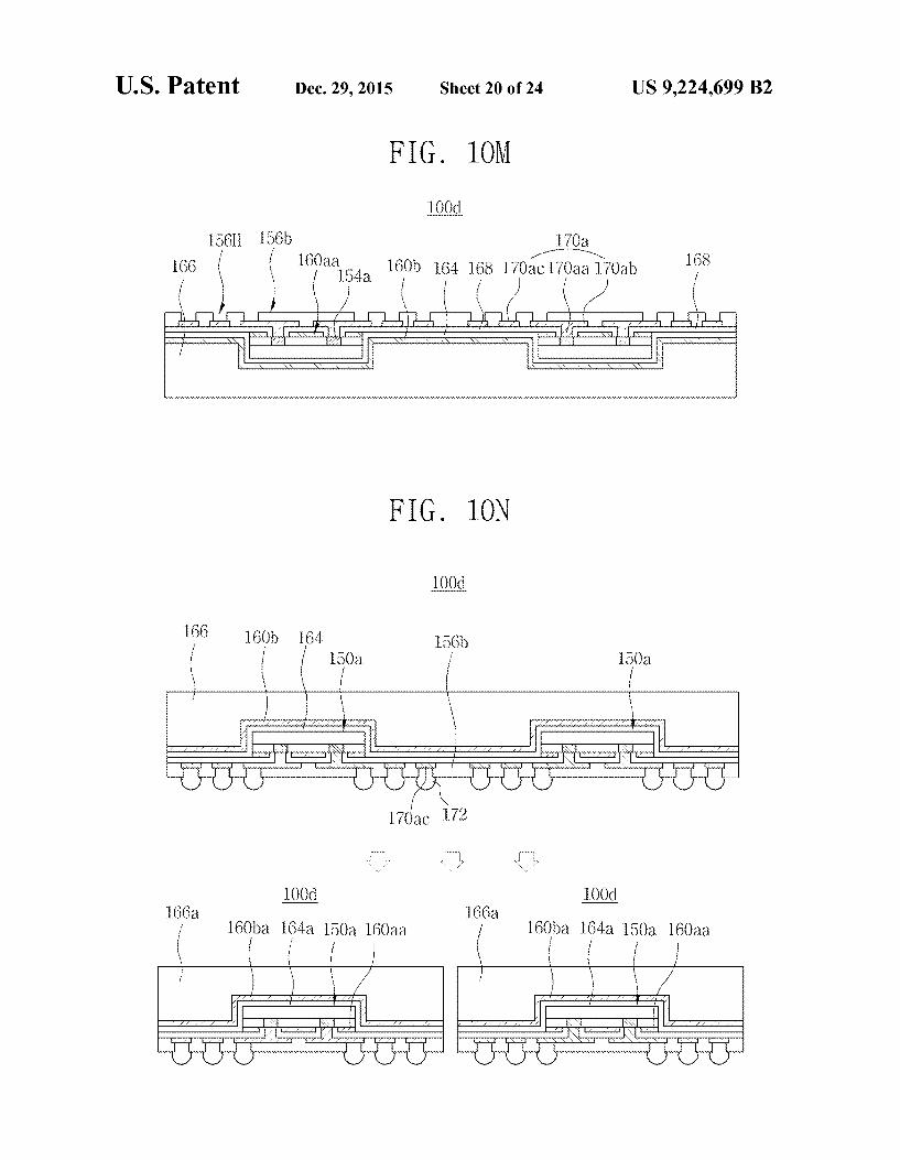
U.S. Patent Dec. 29, 2015 Sheet 20 of 24 US 9.224,699 B2
OOd
156H 156b u170a f fY m
166 ( ( as 160b 164 168 170ác 179aaToab f
FIG. ON
100d
166 160b 164 36) ( ( 50a f 30a
10Od OOd 66a 66a f 60ba 64a .50a 160aa f 16Oba 164a 50a 60aa ( | | | " )

U.S. Patent Dec. 29, 2015 Sheet 21 of 24
FIG 11
150b 160aa 154b. 156a
Pitt U
seriel
72a 170b 17O algobe 17Ob
3.
rter. Irviller
US 9.224,699 B2
6Oba 64ab 68a 156)
156, 150c 154c 156c 174b 166bH
| 100eb N A----- N NSS
GP2C N N sis
OOea---Y
166CH
GP1 (
OOeb-r-r
fic |- tre
N - SS UR triy; ;
- 22 2 7.
E
, EE R 2. -
y Ry
74a 66C 68b. 56d
17Obc 172aa 74b 74a 66C

U.S. Patent Dec. 29, 2015 Sheet 22 of 24 US 9.224,699 B2
FIG 12
500
50 540

U.S. Patent Dec. 29, 2015 Sheet 23 of 24 US 9.224,699 B2

U.S. Patent Dec. 29, 2015 Sheet 24 of 24 US 9.224,699 B2
FIG 15
Forming FiSSures in Wafer
Thinning Wafer SO
SOO
Forming Bonding layer on Wafer S2O
Sectioning Off Layer S30
Forming First Shield Layer S4()
Sectioning Semiconductor Chips S50
Bonding Semiconductor Chips to Substrate Si6O
Forming Second Shield Pattern S70

US 9,224,699 B2 1.
METHOD OF MANUFACTURING SEMCONDUCTOR PACKAGE HAVING
MAGNETC SHIELD UNIT
CROSS-REFERENCE TO RELATED APPLICATION
This application claims priority under 35 U.S.C. S 119 from Korean Patent Application No. 10-2014-0020671 filed on Feb. 21, 2014, the contents of which are incorporated herein by reference in their entirety.
BACKGROUND
1. Field Example embodiments of the inventive concepts relate to a
method of manufacturing a semiconductor package including a magnetoresistive random access memory (MRAM) device.
2. Description of Related Art Various technologies are being proposed for shielding an
external magnetic field Such that a magnetoresistive random access memory (MRAM) device is not influenced by the external magnetic field.
SUMMARY
Example embodiments of the inventive concepts provide a method of manufacturing a semiconductor package config ured such that a magnetoresistor random access memory (MRAM) device is not influenced by an external magnetic field. The technical objectives of the inventive concepts are not
limited to the above disclosure; other objectives may become apparent to those of ordinary skill in the art based on the following descriptions.
In accordance with at least one example of the inventive concepts, a method of manufacturing a semiconductor pack age includes forming cracks in a lattice structure on an active Surface in which electrode terminals are formed, grinding a back Surface of a wafer facing the active surface, bonding a tape on the active surface of the wafer, expanding the tape such that the wafer on the tape is divided as semiconductor chips, forming a shield layer on Surfaces of the semiconductor chips and the tape, cutting the shield layer between the semi conductor chips, and sectioning off each of the semiconduc tor chips which has a first shield pattern formed on a back Surface and sides, bonding the semiconductor chips on a Substrate, and forming a second shield pattern on each of the active Surfaces of the semiconductor chips, wherein the semi conductor chips and the Substrate are physically and electri cally connected by a bonding wire. The forming of the cracks in the lattice structure on the
wafer may include irradiating the active surface of the wafer with a laser beam in the lattice structure.
The bonding of the semiconductor chips to the substrate may include bonding an adhesive film on an upper Surface of the shield layer, forming a first bonding layer on a lower surface of the first shield pattern by contemporaneously or simultaneously cutting the shield layer and the adhesive film, and bonding the first bonding layer to the Substrate. The method may further include forming a buffer layer
between the semiconductor chips and the shield layer. The method may further include forming a molding envel
oping the semiconductor chips and the bonding wire, cutting the molding and the Substrate, and sectioning off a single semiconductor package including each of the semiconductor chips.
10
15
25
30
35
40
45
50
55
60
65
2 The method may further include stacking another semicon
ductor chip with the same structure as the semiconductor chip between the semiconductor chip and the second shield pat tern.
The method may further include forming an inter chip bonding layer between the stacked semiconductor chips to cover one end of the bonding wire and bond the stacked semiconductor chips. The inter chip bonding layer may include epoxy-based
resins and silicon-based resins. The forming of the second shield pattern may include
bonding the second shield pattern which is previously manu factured in the form of a thin film on the surfaces of the semiconductor chips. The first shield pattern and the second shield pattern may
include permalloy that is an alloy of Fe and Ni. In accordance with another example of the inventive con
cepts, a method of manufacturing a semiconductor package includes preparing a wafer having an active surface in which electrode terminals are formed, and a back Surface facing the active surface, forming a first shield layer on the active Sur face excluding the electrode terminals, grinding the back surface of the wafer; cutting the wafer including the first shield layer, and sectioning off each of the semiconductor chips having a first shield pattern formed on the active Sur face, bonding the semiconductor chips to a carrier so that back sides and sides of the semiconductor chips are exposed, forming a second shield layer on the back Surface and sides of the semiconductor chips and an upper Surface of the carrier, forming a molding layer on an upper surface of the second shield layer, and removing the carrier. The forming of the first shield layer may include forming
mask patterns having a wider area than the electrode termi nals and covering the electrode terminals, conformally form ing a first shield layer on a Surface of a protective layer which is not covered by the mask patterns and Surfaces of the mask patterns, and holding the first shield layer only on the Surface of the protective layer by removing the mask patterns. The method may further include forming an interlayer
insulating layer covering the first shield layer and exposing the electrode terminals. The method may further include forming a rewiring unit
including vias connected to the electrode terminals, signal wirings connected to the Vias, and lands connected to the signal wiring and formed in a direction from an edge of the substrate to the outside. The method may further include cutting the molding layer,
the second shield layer, and the rewiring unit between the semiconductor chips, and sectioning offa single semiconduc tor package so that a second shield pattern covering the back Surfaces and sides of the semiconductor chips and a molding covering the second shield pattern are provided.
In accordance with at least one example embodiment, a method of manufacturing a magnetically shielded semicon ductor package includes forming one or more fissures in a lattice structure of a wafer on an active surface thereof, thin ning the wafer, forming a layer at the active Surface of the wafer, sectioning the wafer on the layer into a plurality of sections, each section corresponding to a semiconductor chip, forming a first shield layer on Surfaces of the semiconductor chips and the layer, sectioning off each of the semiconductor chips, each semiconductor chip having an active Surface and a first shield pattern on a back surface and sides thereof, bonding one or more of the semiconductor chips to a Sub

US 9,224,699 B2 3
strate, and forming a second shield pattern on the active Surface of each of the one or more semiconductor chips.
BRIEF DESCRIPTION OF THE DRAWINGS
The foregoing and other example features and advantages of the inventive concepts will be apparent from the more particular description of example embodiments of the inven tive concepts, as illustrated in the accompanying drawings in which like reference characters refer to the same parts throughout the different views. The drawings are not neces sarily to Scale, emphasis instead being placed upon illustrat ing the principles of the inventive concepts. In the drawings:
FIG. 1A is a planar view illustrating a semiconductor pack age according to at least one example embodiment of the inventive concepts, and FIG. 1B is a cross-sectional view taken along the X direction of FIG. 1A:
FIG. 2 is a cross-sectional view illustrating a semiconduc torpackage according to another example embodiment of the inventive concepts;
FIG. 3 is a cross-sectional view illustrating a stack-type semiconductor package according to at least one example embodiment of the inventive concepts;
FIG. 4 is a cross-sectional view illustrating a semiconduc torpackage according to at least one example embodiment of the inventive concepts;
FIG. 5 is a cross-sectional view illustrating a stack-type semiconductor package according to at least one example embodiment of the inventive concepts;
FIGS. 6A to 6G, and 7A to 7L are schematic layouts and cross-sectional views illustrating a method of packaging a memory semiconductor device in process sequence accord ing to at least one example embodiment of the inventive concepts, FIGS. 7A to 7C are cross-sectional views taken along line I-I" of FIGS. 6A to 6C, and FIGS. 7D to 7G are cross-sectional views taken along line II-II' of FIGS. 6D to 6G,
FIGS. 8A to 8D are cross-sectional views illustrating a method of manufacturing a semiconductor package in pro cess sequence according to at least one example embodiment of the inventive concepts:
FIG. 9 is a cross-sectional view illustrating a method of manufacturing a stack-type semiconductor package accord ing to at least one example embodiment of the inventive concepts:
FIGS. 10A to 10N are cross-sectional views illustrating a method of manufacturing a semiconductor package in pro cess sequence according to at least one example embodiment of the inventive concepts:
FIG. 11 is a cross-sectional view illustrating a method of manufacturing a stack-type semiconductor package accord ing to at least one example embodiment of the inventive concepts:
FIG. 12 is a schematic diagram illustrating a semiconduc tor module according to an example embodiment of the inventive concepts including a semiconductor package manu factured according to example embodiments of the inventive concepts:
FIG. 13 is a schematic block diagram illustrating an elec tronic system according to an example; embodiment of the inventive concepts including a semiconductor package manu factured according to example embodiments of the inventive concept; and
FIG. 14 is a schematic diagram illustrating a mobile elec tronic device according to an example embodiment of the
10
15
25
30
35
40
45
50
55
60
65
4 inventive concepts including a semiconductor device manu factured according to example embodiments of the inventive concepts
FIG. 15 is a flow chart illustrating a method of manufac turing a magnetically shielded semiconductor package, according to at least one example embodiment.
DETAILED DESCRIPTION OF THE EMBODIMENTS
Various example embodiments will now be described more fully with reference to the accompanying drawings. These inventive concepts may, however, be embodied in different forms and should not be construed as limited to the example embodiments set forth herein. Although a few example embodiments of the inventive concepts have been shown and described, it would be appreciated by those of ordinary skill in the art that changes may be made in these example embodi ments without departing from the principles and spirit of the inventive concepts, the scope of which is defined in the claims and their equivalents.
It will be understood that when an element is referred to as being “on.” “connected' or “coupled to another element, it can be directly on, connected or coupled to the other element or intervening elements may be present. In contrast, when an element is referred to as being “directly on.” “directly con nected' or “directly coupled to another element, there are no intervening elements present. As used herein the term “and/ or includes any and all combinations of one or more of the associated listed items. Further, it will be understood that when a layer is referred to as being “under another layer, it can be directly under or one or more intervening layers may also be present. In addition, it will also be understood that when a layer is referred to as being “between two layers, it can be the only layer between the two layers, or one or more intervening layers may also be present.
It will be understood that, although the terms “first”, “sec ond', etc. may be used herein to describe various elements, components, regions, layers and/or sections, these elements, components, regions, layers and/or sections should not be limited by these terms. These terms are only used to distin guish one element, component, region, layer or section from another element, component, region, layer or section. Thus, a first element, component, region, layer or section discussed below could be termed a second element, component, region, layer or section without departing from the teachings of example embodiments. The terminology used herein is for the purpose of describ
ing particular example embodiments only and is not intended to be limiting of the invention. As used herein, the singular forms “a,” “an and “the are intended to include the plural forms as well, unless the context clearly indicates otherwise. It will be further understood that the terms “comprises' and/ or “comprising, when used in this specification, specify the presence of stated features, integers, steps, operations, ele ments, and/or components, but do not preclude the presence or addition of one or more other features, integers, steps, operations, elements, components, and/or groups thereof.
In the drawing figures, the dimensions of layers and regions may be exaggerated for clarity of illustration. The same reference numbers indicate the same components throughout the specification. Like numerals refer to like ele ments throughout. As used herein, the term “and/or” includes any and all combinations of one or more of the associated listed items.
Spatially relative terms (e.g., “beneath.” “below,” “lower.” “above.” “upper and the like) may be used herein for ease of

US 9,224,699 B2 5
description to describe one element or a relationship between a feature and another element or feature as illustrated in the figures. It will be understood that the spatially relative terms are intended to encompass different orientations of the device in use or operation in addition to the orientation depicted in the figures. For example, if the device in the figures is turned over, elements described as “below' or “beneath other ele ments or features would then be oriented “above the other elements or features. Thus, for example, the term “below’ can encompass both an orientation that is above, as well as, below. The device may be otherwise oriented (rotated 90 degrees or viewed or referenced at other orientations) and the spatially relative descriptors used herein should be interpreted accord ingly.
Example embodiments are described herein with reference to cross-sectional illustrations that are schematic illustrations of idealized embodiments (and intermediate structures). As Such, variations from the shapes of the illustrations as a result, for example, of manufacturing techniques and/or tolerances, may be expected. Thus, example embodiments should not be construed as limited to the particular shapes of regions illus trated herein but may include deviations in shapes that result, for example, from manufacturing. For example, an implanted region illustrated as a rectangle may have rounded or curved features and/or a gradient (e.g., of implant concentration) at its edges rather than an abrupt change from an implanted region to a non-implanted region. Likewise, a buried region formed by implantation may result in Some implantation in the region between the buried region and the Surface through which the implantation may take place. Thus, the regions illustrated in the figures are schematic in nature and their shapes do not necessarily illustrate the actual shape of a region of a device and do not limit the scope.
Although corresponding plan views and/or perspective views of some cross-sectional view(s) may not be shown, the cross-sectional view(s) of device structures illustrated herein provide support for a plurality of device structures that extend along two different directions as would be illustrated in a plan view, and/or in three different directions as would be illus trated in a perspective view. The two different directions may or may not be orthogonal to each other. The three different directions may include a third direction that may be orthogo nal to the two different directions. The plurality of device structures may be integrated in a same electronic device. For example, when a device structure (e.g., a memory cell struc ture or a transistor structure) is illustrated in a cross-sectional view, an electronic device may include a plurality of the device structures (e.g., memory cell structures or transistor structures), as would be illustrated by a plan view of the electronic device. The plurality of device structures may be arranged in an array and/or in a two-dimensional pattern.
Like reference marks refer to like reference elements throughout. Accordingly, even though the like reference marks or similar reference marks are not referred or explained in the corresponding drawings or figures, the like reference marks or similar reference marks may be explained with reference to other drawings or figures. Further, even though the reference marks are not marked, the reference marks may be explained with reference to other drawings or figures.
FIG. 1A is a planar view illustrating a semiconductor pack age according to at least one example embodiment of the inventive concepts, and FIG. 1B is a cross-sectional view taken along the X direction of FIG. 1A.
Referring to FIGS. 1A and 1B, a semiconductor package 100a according to at least one example embodiment of the
5
10
15
25
30
35
40
45
50
55
60
65
6 inventive concepts may include a Substrate 130a, a semicon ductor chip 110a, a magnetic shield unit SP1, a bonding wire 134a, and a molding 142a. The substrate 130a may include a printed circuit board
(PCB). The PCB may include a base substrate 130aa, a signal wiring unit 132a formed on upper and lower surfaces of the base Substrate 130aa, and upper and lower insulating layers 130ab and 130ac covering the signal wiring unit 132a of the upper and lower surfaces of the base substrate 130aa, respec tively. The signal wiring unit 132a may include Vias 132aa pen
etrating the base Substrate 130aa and transmitting signals, bonding pads 132ab formed on the base substrate 130aa, and lands 132ac formed on the lower surface of the base substrate 130aa. Upper surfaces of the bonding pads 132ab may be exposed, and lower surfaces of the lands 132ac may be exposed. The semiconductor chip 110a may be a memory chip
including magnetoresistive random access memory devices (MRAMs). The semiconductor chip 110a may include elec trode terminals 120a connected to the MRAMs. The semi conductor chip 110a may be configured such that an active surface in which the electrode terminals 120a are formed faces upward. As illustrated in FIG. 1A, the electrode termi nals 120a may be located on edges of the semiconductor chip 110a. The semiconductor chip 110a may be bonded to the upper
surface of the substrate 130a by a first bonding layer 114da. The first bonding layer 114da may be a double-sided tape. The magnetic shield unit SP1 may include a first shield
pattern 118a and a second shield pattern 118b. The first shield pattern 118a may cover a lower surface and sides of the semiconductor chip 110a. The second shield pattern 118b may be formed on an upper Surface (the active surface) of the semiconductor chip 110a. The second shield pattern 118b may be formed on an area excluding areas on which the electrode terminals 120a are formed. The first shield pattern 118a may be formed by a physical
vapor deposition (PVD) method including sputtering. The second shield pattern 118b may be prepared in the form of a thin film which is previously manufactured. The second shield pattern 118b may be bonded to the upper surface of the semiconductor chip 110a by a second bonding layer 114e. The second bonding layer 114e may have, for example, a liquid form, and may be brushed and in adhesion to the surface of the semiconductor chip 110a. The magnetic shield unit SP1 may include permalloy. The
permalloy may be a soft magnetic alloy containing iron (Fe) and nickel (Ni). The permalloy may have considerably high permeability and may thus be easily capable of penetrating a magnetic field. When a wall formed of permalloy is made, an external magnetic field may be absorbed without penetrating the wall. Further, the permalloy may be easily processed. The molding 142a may cover the semiconductor chip
110a. The molding 142a may include epoxy molding com pound (EMC). The bonding wire 134a may physically and electronically
connect the semiconductor chip 110a and the substrate 130a. Specifically, one end of the bonding wire 134a may be bonded to the electrode terminal 120a of the semiconductor chip 110a, and the other end of the bonding wire 134a may be bonded to the bonding pad 132ab of the substrate 130a. The bonding wire 134a may include gold (Au) or aluminum (Al). The semiconductor package 100a according to one
example embodiment of the inventive concepts may further include solder balls 144 bonded to the lands 132ac of the substrate 130a.

US 9,224,699 B2 7
As described above, the semiconductor package 100a according to one example embodiment of the inventive con cepts may include a magnetic shield unit SP1 covering the lower Surface, sides, and upper Surface of the semiconductor chip 110a. The magnetic shield unit SP1 may effectively shield an influx of external magnetic field to the semiconduc tor chip 110a. Accordingly, stable operations of the MRAMs formed in the semiconductor chip 110a can be substantially ensured or secured.
FIG. 2 is a cross-sectional view illustrating a semiconduc torpackage according to another example embodiment of the inventive concepts. Since a semiconductor package 100b according to another example embodiment of the inventive concepts has a construction where the semiconductor chips described above are stacked, a detailed description thereof will be omitted.
Referring to FIG. 2, the semiconductor package 100b according to another example embodiment of the inventive concepts may include a Substrate 130b, Stacked semiconduc torchips 110b and 110c, a magnetic shield unit SP2, bonding wires 134c and 130b, and a molding 142ba.
The substrate 130b may be a PCB. The PCB may include a base substrate 130ba, a signal wiring unit 132a formed on upper and lower surfaces of the base substrate 130ba, and upper and lower insulating layers 130bb and 130bc covering the signal wiring unit 132a at the upper and lower Surfaces of the base substrate 130ba, respectively.
The semiconductor chips 110b and 110c may be sequen tially stacked first and second semiconductor chips 110b and 110c on the substrate 130b. The first and second semiconduc tor chips 110b and 110c may be memory chips including MRAMs. The number of the stacked semiconductor chips may not be limited to two. The first semiconductor chip 110b may include first elec
trode terminals 120b exposed through an active surface, and the second semiconductor chip 110c may include second electrode terminals 120c exposed through the active surface. The magnetic shield unit SP2 may include first shield pat
terns 118a and second shield patterns 118b. The first shield patterns 118a may cover lower surfaces and sides of the first and second semiconductor chip 110b and 110c, respectively. The second shield pattern 118a may cover the upper surface of the second semiconductor chip 110b. The second shield pattern 118b may cover the surface of the second semicon ductor chip 110c excluding an area in which the second electrode terminals 120c are formed as shown in FIG. 1A. The bonding wires 134b and 134c may be a first bonding
wire 134b and a second bonding wire 134c. The first bonding wire 134b may be bonded to the first electrode terminal 120b and the bonding pad 132ab of the substrate 130b. The second bonding wire 134c may be bonded to the second electrode terminal 120c and the bonding pad 132ab of the substrate 13Ob. The semiconductor package 100b according to another
example embodiment of the inventive concepts may further include an inter chip bonding layer 114f compared to the semiconductor package 100a of FIG.1. The inter chip bond ing layer 114fmay be used to stack the first semiconductor chip 110b and the second semiconductor chip 110c on one another. Since the inter chip bonding layer 114fholds ends of the first bonding wires 134b connected to the first semicon ductor chip 110b, breakage of the first bonding wires can be reduced or prevented. The inter chip bonding layer 114fmay include epoxy resin-based adhesive or silicon-based adhesive capable of coating in a liquid or paste form.
In the above example structure, the second shield pattern 118b may be bonded to the upper surface of the semiconduc
10
15
25
30
35
40
45
50
55
60
65
8 tor chip 110c which is located in the uppermost layer regard less of the number of the stacked semiconductor chips 110b and 110C. An effect of a magnetic field capable of occurring between
the semiconductor chips 110b and 110c stacked up and down can be shielded by the second shield pattern 118b formed on the lower surface and the sides of the second semiconductor chip 110c. Accordingly, even when the semiconductor chips (memory chips) are stacked, the magnetic field can be shielded from each other by the magnetic shield unit SP2. A stack-type semiconductor package according to another
example embodiment including the semiconductor package in which a magnetic shield unit (the first shield patternand the second field pattern) described above is formed will be described below with reference to accompanying drawings.
FIG. 3 is a cross-sectional view illustrating a stack-type semiconductor package according to another example embodiment of the inventive concepts.
Referring to FIG.3, a semiconductor package 100c accord ing to another example embodiment of the inventive concepts may have a structure in which semiconductor packages 100.ca and 100cb are stacked.
For example, the semiconductor package 100c according to another example embodiment of the inventive concepts includes a first semiconductor package 110ca, a second semi conductor package 110cb, and a package connection bump 144aa. The first semiconductor package 100ca may include a first
substrate 130c, a first semiconductor chip 110bstacked on the first substrate 130c, a magnetic shield unit SP2, bonding wires 134b and 134c, and a first molding 142ba. The first substrate 130c may include a first base substrate
130ca, and a first signal wiring unit 132b formed on upper and lower surfaces of the first base substrate 103ca. The first signal wiring unit 132b may include a first bonding pad 132bb formed on the upper surface of the first base substrate 130ca. and a first bump land 132bd formed on a lower surface of the first base substrate 130ca. The first and second semiconductor chips 110b and 110c
may be memory chips including MRAMs. The magnetic shield unit SP2 may include first shield pat
terns 118a covering lower surfaces and sides of the first and second semiconductor chips 110b and 110c, and a second shield pattern 118b formed on an upper surface of the semi conductor chip 110c which is located on the uppermost layer. The bonding wires 134b and 134c may include a first
bonding wire 134b and a second bonding wire 134c. The first bonding wire 134b may be bonded to the first semiconductor chip 110b and the substrate 130c, and the second bonding wire 134c may be bonded to the second semiconductor chip 110C and the Substrate 130c. The second semiconductor package 100cb may include a
second substrate 130d, a third semiconductor chip 110d, a third bonding wire 134d. and a second molding 142bb. The second substrate 130d may include a second base
substrate 130da, and a second signal wiring unit 132c formed on upper and lower Surfaces of the second base substrate 130da. The second signal wiring unit 132C may include a second
bonding pad 132cb and a second bump land 132cd formed on an upper surface of the second base substrate 130da, and lands 132cc formed at a lower surface of the second base substrate 130da. The third semiconductor chip 110d may be a logic semi
conductor chip. The third semiconductor chip 110d may be formed such that an active surface thereof faces upward.

US 9,224,699 B2 9
Third electrode terminals 120d, which may be electrode ter minals of logic elements, may beformed in the active surface. One end of the third bonding wire 134d may be bonded to
the third electrode terminal 120d of the third semiconductor chip 110d, and the other end of the third bonding wire 134d may be bonded to the second bonding pad 132cb of the Substrate 130d. The second molding 142bb may include a through hole
142bH formed to be correspond to the second bump land 132cd. Abottom surface of the through hole 142bH may bean upper surface of the second bump land 132cd.
The second semiconductor package 130cb may further include solder balls 144b which are in contact with lower surfaces of the lands 132CC. The first and second semiconductor packages 100.ca and
100cb may be physically and electrically connected through a package connection bump 144aa. The package connection bump 144aa may fill the through
hole 142bH of the second molding 142bb. The package con nection bump 144aa may be bonded to the first bump land 132bd of the first semiconductor package 100ca and the sec ond bump land 132cd of the second semiconductor package 100ch. The stack-type semiconductor package 100c according to
another example embodiment of the inventive concepts may have a structure that every surface of the first and second semiconductor chips 110b and 110c including the MRAMs is covered by the magnetic shield unit SP2 (the first shield patterns 118a and the second shield pattern 118b). An influx of an external magnetic field to the first and second semicon ductor packages 110b and 110c may be effectively shielded by the magnetic shield unit SP2.
Accordingly, a stable operation of the stack-type semicon ductor package according to another example embodiment of the inventive concepts can be secured.
FIG. 4 is a cross-sectional view illustrating a semiconduc torpackage according to another example embodiment of the inventive concepts.
Referring to FIG. 4, a semiconductor package 100d according to another example embodiment of the inventive concepts includes a semiconductor chip 150a, a semiconduc tor chip support unit GP, a magnetic shield unit SP3, and a molding 166a. The semiconductor chip 150a may be a memory chip
including MRAMs. The semiconductor chip 150a may include electrode terminals 154a connected to the MRAMs, and a first protective layer 156a surrounding the electrode terminals 154a.
The semiconductor chip Support unit GP may include an interlayer insulating layer 168, a rewiring unit 170a, and a second protective layer 156b, which are sequentially stacked. The rewiring unit 170a may include vias 170aa which
penetrates the interlayer insulating layer 168 and is physically or electrically connected to the semiconductor chip 150a, signal wirings 170ab connected to the vias 170aa, and lands 170ac connected to one end of the signal wirings 170ab. The lands 170ac may beformed in the direction from edges of the semiconductor chip 150a to edges of the semiconductor package 100d. The interlayer insulating layer 168 and the rewiring unit 170a may alternately beformed in a multi-layer. The semiconductor chip supportunit GP may be stacked on
a lower surface of the semiconductor chip 150a. Specifically, the lower surface (an active surface) of the semiconductor chip 150a may face one surface of the interlayer insulating layer 168. The electrode terminals 154a of the semiconductor chip 150a may be physically or electrically connected to the vias 170aa of the rewiring unit 170a.
10
15
25
30
35
40
45
50
55
60
65
10 The magnetic shield unit SP3 may include a first shield
pattern 160aa and a second shield pattern 160ba. The first shield pattern 160aa may be formed on a lower surface of the active surface of the semiconductor chip 150a. The first shield pattern 160aa may be formed on a lower surface of the first protective layer 156a. The first shield pattern 160aa may include first through holes 160aH for exposing surfaces of the electrode terminals 154a. The first through hole 160aH may have a greater area than the electrode terminal 154a. A lower surface of the first shield pattern 160aa may be in
contact with the interlayer insulating layer 168. The interlayer insulating layer 168 may include a second through hole 168H. The second through hole 168H may have a smaller area than the electrode terminal 154a. Accordingly, the interlayer insu lating layer 168 may cover an upper Surface and sides of the first shield pattern 166aa. The second shield pattern 160ba may cover the upper
surface and sides of the semiconductor chip 150a, and may extend to an upper Surface of the semiconductor chip Support unit GP on which the semiconductor chip 150a is not located. The first shield pattern 160aa and the second shield pattern
160ba may be formed through a PVD process including a sputter. The molding 166a may be in contact with an upper Surface
of the second shield pattern 166bb. The molding 166a may include EMC. The semiconductor package 100d according to another
example embodiment of the inventive concepts may further include a buffer pattern 164a formed between the second shield pattern 160ba, and the semiconductor chip 150a and the semiconductor chip support unit GP. The buffer pattern 164a may include a silicon oxide and a silicon nitride. The semiconductor package 100d according to another
example embodiment of the inventive concepts may include solder balls 172 which penetrate the second protective layer 156d and are in contact with the lands 170ac. As described above, the semiconductor package 100d
according to another example embodiment of the inventive concepts may include a structure that does not use an addi tional Substrate and rearranges a signal wiring to the outside through a rewiring process in a wafer level. Accordingly, a size of the semiconductor package can be minimized, a pack age process can be simplified, and a yield can be improved. The semiconductor package 100d according to another
example embodiment of the inventive concepts may include a magnetic shield unit SP3 covering an entire surface of the semiconductor chip 150a. An influx of an external magnetic field to the semiconductor chip 150a can be effectively shielded by the magnetic shield unit SP3. Accordingly, stable operations of the MRAMs included in the semiconductor chip 150a can be secured.
Hereinafter, a stack-type semiconductor package accord ing to another example embodiment of the inventive concepts including the semiconductor package in which the magnetic shield unit is formed as described above will be described with reference to accompanying drawings.
FIG. 5 is a cross-sectional view illustrating a stack-type semiconductor package according to another example embodiment of the inventive concepts.
Referring to FIG. 5, a stack-type semiconductor package 100e according to another example embodiment of the inven tive concepts may have a structure that semiconductor pack ages 100ea and 100eb are stacked.
For example, the stack-type semiconductor package 100e according to another example embodiment of the inventive

US 9,224,699 B2 11
concepts may include a first semiconductor package 100ea, a second semiconductor package 100eb, and package connec tion bumps 172aa.
The first semiconductor package 100ea may include a first semiconductor chip 150b, a first semiconductor chip support unit GP1, a magnetic shield unit SP3, and a first molding 166b. The first semiconductor chip 150b may be a memory chip
including MRAMs. The first semiconductor chip 150b may include a first electrode terminal 154b formed at an active surface, and a first protective layer 156a surrounding the first electrode terminal 154b. The first semiconductor support unit GP1 may include a
first interlayer insulating layer 168a, a first rewiring unit 170b, and a second protective layer 156b. The first rewiring unit 170b may include first vias 170ba, first signal wirings 170bb, and first bump lands 170bc. The second semiconductor package 100eb may include a
second semiconductor chip 150c, a second semiconductor chip Support unit GP2, land connection bumps 174a, second bump lands 174b, and a second molding 166c.
The second semiconductor chip 150c may be a logic chip. The second semiconductor chip 150c may include second electrode terminals 154c formed on an active surface, and a third protective layer 156c surrounding the second electrode terminal 154c.
The second semiconductor chip 150c may be formed such that the second electrode terminals 154c of logic elements face the second semiconductor chip support unit GP2. The second semiconductor chip support unit GP2 may
include a second interlayer insulating layer 168b, second rewiring units 170c, and a fourth protective layer 156d which are sequentially stacked. The second rewiring unit 170c may include second vias
170ca which penetrate the second interlayer insulating layer 168b and are physically and electrically connected to the second semiconductor chip 150c, second signal wirings 170cb connected to the second vias 170ca, and lands 170cc connected to ends of the second signal wirings 170cb. The lands 170cc may be formed in the direction from edges of the second semiconductor chip 150c to edges of the second semi conductor package 100eb. The second interlayer insulating layer 168b and the second rewiring units 170c may be alter nately formed in a multi-layer. The second semiconductor chip supportunit GP2 may be
stacked on a lower Surface of the second semiconductor chip 150c. Second electrode terminals 154c of the second semi conductor chip 150c may be physically and electrically con nected to the vias 170ca of the second wiring units 170c. The second molding 166c may include EMC. The second
semiconductor package 100e may include a through hole 166cH which penetrates the second molding 166c. The through hole 166cH may beformed on an upper surface of the lands 170cc disposed adjacent to the edge of the second semiconductor package 100e. A bottom surface of the through hole 166cH may be an upper surface of the lands 17Occ. The land connection bump 174a may be in contact with the
lands 170cc, and fill the through hole 166cH. The second bump lands 174b may be formed on a surface
of an upper surface of the second molding 166c which face the lands 170cc. Accordingly, the land connection bump 174a may be physically and electrically connected to the lands 170cc and the second bump lands 174b. The first and second semiconductor packages 100ea and
100eb may be physically and electrically connected through the package connection bump 172aa.
10
15
25
30
35
40
45
50
55
60
65
12 The package connection bump 172aa may be bonded to the
first bump lands 170bc of the first semiconductor package 100ea and the second bump lands 174b of the second semi conductor package 100eb.
FIGS. 6A to 6G, and 7A to 7I are schematic layouts and cross-sectional views illustrating a method of packaging a memory semiconductor device in process sequence accord ing to at least one example embodiment of the inventive concepts, and FIGS. 7A to 7C are cross-sectional views taken along line I-I" of FIGS. 6A to 6C, and FIGS. 7D to 7G are cross-sectional views taken along line II-II' of FIGS. 6D to 6G.
Referring to FIGS. 6A and 7A, a method of manufacturing the semiconductor package 100a according to at least one example embodiment of the inventive concepts may include irradiating an active surface AS of an wafer 110 on which a plurality of MRAMs with a laser beam are formed, and bond ing a first tape 114a to the active surface AS. The active surface AS of the wafer 110 may be an upper
surface of areas in which the MRAMs are formed. The irra diating of the laser beam may include irradiating with the laser beam in horizontal and vertical directions in consider ation of a desired, or alternatively predetermined chip size to the active surface AS. The irradiating of the laser beam, as shown in FIG. 7A, may
include a crack or fissure CR which is generated from the active Surface AS to a constant depth. The bonding of the first tape 114a may include bonding a
backgrinding type tape to the active Surface AS on which the laser beam is radiated. The backgrinding type tape 114a may prevent the active surface AS of the wafer 110 from being damaged or contaminated by foreign substances. The back grinding type tape 114a may include polyvinyl chloride (PVC).
Referring to FIGS. 6B and 7B, the method of manufactur ing the semiconductor package 100a according to at least one example embodiment of the inventive concepts may include grinding a back surface of the wafer 110. The grinding of the back Surface may be grinding the back
surface of the wafer 110 in order to make a thickness of the wafer 110 uniform. In this case, the thickness of the wafer 110 may be in a range of 0.2 mm to 0.51 mm.
During grinding of the back surface, as shown in FIG. 7B, the thickness of the wafer 110 may be decreased from a thickness d1 to a thickness d2, and the crack or fissure CR generated by the irradiation of the laser beam, which is a previous process, may extend to the back Surface of the ground wafer 110.
Referring to FIGS. 6C and 7C, the method of manufactur ing the semiconductor package 100a according to at least one example embodiment of the inventive concepts may include bonding a second tape 114b to the back surface of the wafer 110. A method of the semiconductor package 100a according to an example embodiment of the inventive concepts may include removing the first tape 114a after bonding the second tape 114b.
Further, the method of manufacturing the semiconductor package 100a according to an example embodiment of the inventive concepts, after bonding a third tape 114c to the active surface AS where the first tape 114a was removed, may include exposing the back surface BS of the wafer 110 by removing the second tape 114b. The second tape 114b and the third tape 114c may be
protective tapes. The protective tape may include PVC. Referring to FIGS. 6D and 7D, the method of manufactur
ing the semiconductor package 100a according to at least one example embodiment of the inventive concepts may include

US 9,224,699 B2 13
expanding or elongating the third tape 114c Such that the wafer 110 on the third tape 114c shown in FIGS. 6C and 7C is divided as semiconductor chips 110a. The expanding of the third tape 114c may include pulling
edges of the third tape 114c with a constant strength in a direction parallel to the active surface AS.
While the third tape 114c is expanded in all directions, the wafer 110 may be divided into the semiconductor chips 110a by the cracks CR, which are expanded to the back surface BS of the wafer 110. The semiconductor chips 110a may be aligned with a constant distance therebetween by the expanded third tape 114c.
Referring to FIGS. 6E and 7E, the method of manufactur ing the semiconductor package 100a according to at least one example embodiment of the inventive concepts may include stacking a buffer layer 116 and a shield layer 118 on the semiconductor chips 110a bonded to the third tape 114c. The buffer layer 116, as shown in FIG. 7E, may beformed
on the exposed back surfaces BS and sides of the semicon ductor chips 110a, and on an exposed upper Surface of the third tape 114c between the semiconductor chips 110a.
The buffer layer 116 may include an insulating layer. The insulating layer may include the silicon oxide (SiO) and the silicon nitride (SiN). The shield layer 118 may include a material with high
permeability. The shield layer 118 may include permalloy. The permalloy may be a soft magnetic alloy containing Fe and Ni. The permalloy may have considerably high perme ability and characteristics of easily penetrating a magnetic field. When a wall is formed of the permalloy, an external magnetic field may be absorbed in and not penetrate the wall. Further, the permalloy may be easily processed. The method of forming the permalloy may include the
PVC process including a sputter. Referring to FIGS. 6F and 7F, the method of manufacturing
the semiconductor package 100a according to at least one example embodiment of the inventive concepts may include bonding a fourth tape 114d to a surface of the shield layer 118. The fourth tape 114d may be a double-sided bonding tape. The double-sided bonding tape may be a die attached film (DAF) used in a semiconductor package process.
Referring to FIGS. 6G and 7G, the method of manufactur ing the semiconductor package 100a according to at least one example embodiment of the inventive concepts may include sectioning off each of the semiconductor chips 110a having the buffer layer 116 and the shield layer 118.
The sectioning off of each of the semiconductor chips 110a may include sectioning off each of the semiconductor chips 110a by irradiating the laser beam between the semiconduc torchips 110a. While sectioning off each of the semiconduc tor chips 110a, the buffer layer 116, the shield layer 118, and the fourth tape 114 shown in FIG. 6F are cut.
Accordingly, a buffer pattern 116a, a first shield pattern 118a, and a first bonding layer 114da may be stacked on the back surface BS of the semiconductor chips 110a, and the active surface AS of the semiconductor chips 110a and upper surfaces of the electrode terminals 120a of the MRAMs may be exposed.
Referring to FIG. 7H, the method of manufacturing the semiconductor package 100a according to at least one example embodiment of the inventive concepts may include bonding the semiconductor chips 110a to a substrate 130a.
The semiconductor chips 110a may be bonded to the sub strate 130a through a first bonding layer 114da bonded to the back surface BS of the semiconductor chips 110a.
The substrate 130a may include a printed circuit board (PCB). The PCB may include a base substrate 130aa, a signal
10
15
25
30
35
40
45
50
55
60
65
14 wiring unit 132a formed on upper and lower surfaces of the base Substrate 130aa, and upper and lower insulating layers 130ab and 130ac covering the signal wiring unit 132a formed on the upper and lower surfaces of the base substrate 130a, respectively. The signal wiring unit 132a may include Vias 132aa for
transferring signals through the base Substrate 130aa, bond ing pads 132ab formed on the base substrate 130aa, and lands 132ac formed on the lower surface of the base substrate 130aa. Upper surfaces of the bonding pads 132ab and lower surfaces of the lands 132ac may be exposed.
Referring to FIG. 7I, the method of manufacturing the semiconductor package 100a according to at least one example embodiment of the inventive concepts may include adding bonding wires 134a for physically and electrically connecting between the semiconductor chip 110a and the substrate 130a. The bonding wires 134a may be bonded to the electrode
terminals 120a of the semiconductor chips 110a and to the bonding pads 132ab of the substrate 130a. The bonding wires 134a may include gold (Au) or alumi
num (Al). Referring to FIG. 7J, the method of manufacturing the
semiconductor package 100a according to at least one example embodiment of the inventive concepts may include bonding a second shield pattern 118b to the upper surface of the semiconductor chip 110a. The second shield pattern 118b may include a material
with high permeability. The second shield pattern 118b may be bonded in the form of a thin film. The second shield pattern 118b may include permalloy that
is an alloy of Fe and Ni. The second shield pattern 118b may be bonded on the
upper surface of the semiconductor chip 110a by a second bonding layer 114e. The second bonding layer 114e may have a liquid form, and may be applied and adhere to the Surface of the semiconductor chip 110a. The second shield pattern 118b may cover the upper sur
face of the semiconductor chip 110a excluding an area in which the electrode terminals 120a are formed.
Referring to FIG. 7K, the method of manufacturing the semiconductor package 100a according to at least one example embodiment of the inventive concepts may include forming a molding layer 142a for sealing the semiconductor chips 110a. The forming of the molding layer 142a may include form
ing and curing a molding material on an entire Surface of the substrate 130a. The molding layer 142a may protect the semiconductor
chip 110a from external shocks and contaminants. The mold ing layer 142a may include an epoxy molding compound (EMC).
Referring to FIG. 7L, the method of manufacturing the semiconductor package 100a according to at least one example embodiment of the inventive concepts may include forming solder balls 144 on the lower surface of the substrate 130a, and sectioning off a single semiconductor package 100a including each of the semiconductor chips 110a. The forming of the solder balls 144 may include bonding
the solder balls 144 to the lands 132ac of the substrate 130a. The sectioning off of the single semiconductor package
100a may include simultaneously cutting the substrate 130a and the molding layer 142a. Each sectioned offmolding layer 142aa in the single semiconductor package 100a is referred to as a molding 142aa. The sectioning off of each single semiconductor package
100a may be performed using, for example, a sawing process,

US 9,224,699 B2 15
a drilling process, and/or a cutting process. Through the sec tioning off of each single semiconductor package 100a, the semiconductor package 100a according to one example embodiment of the inventive concepts may be formed.
Hereinafter, a method of manufacturing a semiconductor package 100b according to another example embodiment of the inventive concepts where the semiconductor chips on which the above-mentioned first and second shield patterns 116a and 118a are formed are stacked will be described with reference to accompanying drawings.
FIGS. 8A to 8D are cross-sectional views illustrating a method of manufacturing a semiconductor package in pro cess sequence according to another example embodiment of the inventive concepts.
Since processes prior to processes described below are similar to or the same as to the processes of FIGS. 7A to 7I, a detailed description will be omitted.
Referring to FIG. 8A, a method of manufacturing a semi conductor package 100b according to another example embodiment of the inventive concepts may include bonding a first semiconductor chip 110b to a substrate 130b, and bond ing a first boding wire 134b between the first semiconductor chip 110b and the substrate 130b. The first semiconductor chip 110b may be bonded to the
substrate 130b through a first bonding layer 114da. The buffer patterns 164a and the first shield pattern 118a formed through the processes of FIGS. 7A to 7E are sequentially stacked on back surface and sides of the semiconductor chip 110b. Accordingly, the first bonding layer 114da may be in contact with the first shield pattern 118a and an upper insulating layer 130ba of the Substrate 130b. The substrate 130b may be a PCB. The substrate 130b may
include bonding pads 132ab exposed upward from the sub strate 130b, and lands 132ac exposed downward from the substrate 130b. The bonding pads 132ab may have wider exposed areas than the bonding pads 132ab of the semicon ductor package 100a described above. The buffer pattern 116a may include silicon nitride (SiNx)
and silicon oxide (SiO2). The first shield pattern 118a may include a material with high permeability. The first shield pattern 118a may include permalloy that is an alloy of Fe and Ni.
The bonding of the first bonding wire 134b may include bonding first electrode terminals 120b of the first semicon ductor chip 110b and the bonding pads 132ab,
Referring to FIG. 8B, the method of manufacturing a semi conductor package 100b according to another example embodiment of the inventive concepts may include Stacking a second semiconductor chip 110c on an upper Surface of the first semiconductor chip 110b, and bonding a second bonding wire 134c between the second semiconductor chip 110c and the Substrate 130b.
The stacking of the second semiconductor chip 110c may include forming an inter chip bonding layer 114f on the upper surface of the first semiconductor chip 110b to which ends of the first bonding wires 134b are bonded, and bonding the second semiconductor chip 110c on the upper surface of the first semiconductor chip 110b.
Abuffer pattern 116a and a first shield pattern 118a may be formed, for example sequentially formed, on a back Surface and sides of the second semiconductor chip 110c.
Since the inter chip bonding layer 114fholds one end of the first bonding wire 134b connected to the first electrode ter minal 120b of the first semiconductor chip 110b, the inter chip bonding layer 114fmay be coated in a liquid or paste form. The inter chip bonding layer 114fmay include epoxy resin-based adhesive or silicon-based adhesive.
5
10
15
25
30
35
40
45
50
55
60
65
16 The bonding of the second bonding wire 134c may include
bonding one end of the second bonding wire 134c to the second electrode terminal 120c of the second semiconductor chip 110c, and bonding the other end of the second bonding wire 134c to the bonding pads 132ab of the substrate 130b.
Referring to FIG. 8C, the method of manufacturing a semi conductor package 100b according to another example embodiment of the inventive concepts may include forming the second shield patterns 118b on the upper surfaces of the second semiconductor chip 110c, respectively, and forming the molding layer 142b covering the second shield patterns 118b and the stacked semiconductor chips 110b and 110c. The second shield patterns 118b may include a material
with high permeability. The second shield patterns 118b may include permalloy that is an alloy of Fe and Ni. The second shield patterns 118b may be previously manu
factured in the form of a thin film, and be bonded to the upper surface of the second semiconductor chip 110c through the second bonding layer 114e.
Referring to FIG.8D, the method of manufacturing a semi conductor package 100b according to another example embodiment of the inventive concepts may include forming solder balls 144 on a lower surface of the substrate 130b, and sectioning off a single semiconductor package 100b includ ing each of the stacked semiconductor chips 110b and 110c. The forming of the solder balls 144 may include bonding
the solder balls 144 to the lands 132ac of the substrate 130b. The sectioning off of the single semiconductor package
100b may include simultaneously cutting the substrate 130b and the molding layer 142b. Each of the sectioned off mold ing layer 142ba in the single semiconductor package 100b is referred to as a molding 142ba. The sectioning off of the single semiconductor package
100b may be performed using, for example, a sawing process, a drilling process, and/or a cutting process. Through the sec tioning off of the single semiconductor package 100b, the semiconductor package 100b according to another example embodiment of the inventive concepts may be formed.
In another example embodiment described above, an example of stacking two semiconductor chips are described, but the number of the stacked semiconductor chips is not limited to two.
Hereinafter, a method of manufacturing a stack-type semi conductor package 100c including semiconductor packages 100b manufactured according to another example embodi ment described above will be described with reference to accompanying drawings.
FIG. 9 is a cross-sectional view illustrating a method of manufacturing a stack-type semiconductor package 100c according to an example embodiment of the inventive con cepts.
Referring to FIG. 9, a method of manufacturing a stack type semiconductor package 100c according to an example embodiment of the inventive concepts may include manufac turing the first semiconductor package 100.ca and the second semiconductor package 100cb individually, and Stacking the first and second semiconductor packages 100ca and 100cb on each other.
Since the method of manufacturing the first semiconductor package 100ca was described with reference to FIGS. 8A to 8D, description will be briefly provided. The method of manufacturing the first semiconductor
package 100.ca according to an example embodiment of the inventive concepts may include bonding a first semiconduc torchip 110b to a first substrate 130c, bonding a first bonding wire 134b to the first semiconductor chip 110b and the first substrate 130c. stacking a second semiconductor chip 110c

US 9,224,699 B2 17
on the first semiconductor chip 110b, bonding a second bond ing wire 134c to the second semiconductor chip 110C and the substrate 130c, and bonding a second shield pattern 118b to an upper Surface of the second semiconductor chip 110c. The first semiconductor chip 110b and the second semi
conductor chip 110C may be memory chips including MRAMs. A buffer pattern 116a and a first shield pattern 118a may be formed on a back surface and sides of the first and second semiconductor chips 110b and 110c, and the second shield pattern 118b may be bonded and formed on the upper surface of the second semiconductor chip 110c. The first substrate 130c may include a first base substrate
130ca, and a first signal wiring unit 132b formed on upper and lower surfaces of the first base substrate 130ca. The first signal wiring unit 132b may include a first bonding pad 132bb formed on the upper surface of the first base substrate 130ca. and a first bump land 132bd formed on the lower surface of the first base substrate 130ca.
Further, the method of manufacturing the first semiconduc tor package 100ca may include forming a first molding 142ba, and bonding first solder balls 144a to lower surface of the first bump land 132bd exposed downward from the first Substrate 130C. The second semiconductor package 100cb may be manu
factured by a method of manufacturing a general semicon ductor package. For example, the method of manufacturing the second semiconductor package 100cb according to an example embodiment of the inventive concepts may include bonding a third semiconductor chip 110d to a second sub strate 130d, and contemporaneously or simultaneously bond ing a third bonding wire 134d to the third semiconductor chip 110d and the second substrate 130d. The third semiconductor chip 110d may be a logic semi
conductor chip in which a logic device is formed. Electrode terminals 120d of the logic device may be exposed through an active surface of the third semiconductor chip 110d. The second substrate 130d may include a second base
substrate 130da, and a second signal wiring unit 132c formed on upper and lower Surfaces of the second base substrate 130da. The second signal wiring unit 132C may include a second
bonding pad 132cb and a second bump land 132cd formed on the upper surface of the second base substrate 130da, and lands 132cc formed the lower surface of the second base substrate 130da. The method of manufacturing the second semiconductor
package 100cb according to an example embodiment of the inventive concepts may include forming a second molding 142bb, and forming a through hole 142bH in the second molding 142bb. A bottom surface of the through hole 142bH may be an upper surface of the second bump land 132cd. The method of manufacturing the second semiconductor
package 100cb according to an example embodiment of the inventive concepts may include bonding second solder balls 144b to the lands 132C. The stacking of the first semiconductor package 100.ca and
the second semiconductor package 100cb may include form ing a package connection bump 144aa by reflowing the first solder ball 144a. The package connection bump 144aa may fill the through
holes 142bH of the second molding 142bb. The package connection bump 144aa may physically and electrically con nect the first and second semiconductor packages 100.ca and 100ch.
Hereinafter, a method of manufacturing a semiconductor package including the magnetic shield unit formed by the
10
15
25
30
35
40
45
50
55
60
65
18 method according to an example embodiment of the inventive concepts will be described with reference to accompanying drawings.
FIGS. 10A to 10N are cross-sectional views illustrating a method of manufacturing a semiconductor package in pro cess sequence according to an example embodiment of the inventive concepts.
Referring to FIG. 10A, a method of manufacturing a semi conductor package 100d according to an example embodi ment of the inventive concepts may include bonding a first tape 152a to a back surface BS of a wafer 150. The other surface of the wafer 150 to which the first tape
152 is not bonded may be an active surface AS. The wafer 150 may include MRAMs formed from the
active surface AS to a constant depth. The wafer 150 may be formed on the active surface AS, and may include electrode terminals 154a which are physically and electrically con nected to the MRAMS.
Further, the wafer 150 may include a first protective layer 156a surrounding sides of the electrode terminals 154a. The first protective layer 156a may be formed in the form of Surrounding sides excluding Surfaces of the electrode termi nals 154a. The first protective layer 156 may include a photosensitive
polyimide resin. Referring to FIG. 10B, the method of manufacturing the
semiconductor package 100d according to an example embodiment of the inventive concepts may include forming mask patterns 158 covering exposed surfaces of the electrode terminals 154a. A lower surface of each of the mask patterns 158 may have
a wider area than the upper surface of each of electrode terminals 154a. The forming of the mask patterns 158 may include photolithography. The mask patterns 158 may include a photoresist.
Referring to FIG. 10C, the method of manufacturing the semiconductor package 100d according to an example embodiment of the inventive concepts may include forming a first shield layer 160a on the upper surface of the wafer 150 on which the mask patterns 158 are formed. The first shield layer 160a may be formed on surfaces of
the first protective layer 156a and the mask patterns 158. Although not shown, the first shield layer 160a may be dis continuously formed on sides of the mask patterns 158. The first shield layer 160a may include a material with high
permeability. The first shield layer 160a may include permal loy. The permalloy may be an alloy of Fe and Ni. A method of forming the first shield layer 160a may include a PVD process including a sputter.
Referring to FIG. 10D, the method of manufacturing the semiconductor package 100d according to an example embodiment of the inventive concepts may include removing the mask patterns 158 shown in FIG. 10C. The removing of the mask patterns 158 may include a
lift-off process. While the mask patterns 158 are removed through the lift-off process, the first shield layers 160a formed on the sides and upper Surfaces of the mask patterns 158 shown in FIG. 10C may be simultaneously removed.
Accordingly, the electrode terminals 154a may be exposed, in the first shield layer 160a, and only the upper surface of the first protective layer 156a excluding the sur faces of the electrode terminals 154a may remain. The sides of the first protective layer 156a and the sides of the first shield layer 160a may not be vertically aligned. The sides of the first shield layer 160a may be located on the upper surface of the first protective layer 156a.

US 9,224,699 B2 19
Referring to FIG. 10E, the method of manufacturing the semiconductor package 100d according to an example embodiment of the inventive concepts may include bonding a second tape 152b on the active surface AS of the wafer 150, and grinding the back surface BS of the wafer 150.
Further, after bonding the second tape 152a, the method of manufacturing the semiconductor package 100d according to an example embodiment of the inventive concepts may include removing the first tape 152a shown in FIG. 10D beforegrinding the back surface of the wafer 150. The second tape may be a back grinding tape. The back grinding tape 152b may include PVC.
Through the grinding of the back surface of the wafer 150, a thickness of the wafer 150 may become thin and uniform. The thickness of the wafer 150 may be in a range of 0.2 mm to 0.51 mm.
The method of manufacturing the semiconductor package 100d according to an example embodiment of the inventive concepts may also include removing the second tape 152b from the wafer 150, and performing a cleaning process.
Referring to FIG. 10F, the method of manufacturing the semiconductor package 100d according to an example embodiment of the inventive concepts may include section ing off the wafer 150 of FIG. 10E as a plurality of semicon ductor chips 150a. The sectioning off of the wafer 150 may be performed
using, for example, a sawing process, a drilling process, and/ or a cutting process. A first shield pattern 160aa may be formed on an upper
surface of each of individual semiconductor chips 150a by the cutting of the first shield layer 160a shown in FIG. 10E.
Referring to FIG. 10G, the method of manufacturing the semiconductor package 100d according to an example embodiment of the inventive concepts may include bonding the semiconductor chips 150a to an upper surface of a carrier 162. The semiconductor chips 150a may be bonded to the car
rier 162 through a third tape 152c bonded to the upper surface of the carrier 162. The carrier 162 may include steel use stainless (SUS),
glass, and a wafer. The third tape 152c may be a double-sided tape. Specifically, the third tape 152c may include a film 152ca, a first adhesive coating layer 152cb coated on one side of the film 152ca and including bubbles, and a second adhe sive coating layer 152cc coated on the other side of the film 152ca. The first adhesive coating layer 152cb may be in contact with the first shield patterns 160aa of the semicon ductor chips 150a. The first adhesive coating layer 152cb may have character
istics in which internal bubbles are expanded by heat or light. Referring to FIG. 10H, the method of manufacturing the
semiconductor package 100d according to an example embodiment of the inventive concepts may include forming a buffer layer 164 and a second shield layer 160b on back surface and sides of the semiconductor chips 150a. The buffer layer 164 may include an insulating layer. The
buffer layer 164 may include silicon oxide (SiO) and silicon nitride (SiNx). The second shield layer 160b may include a material with
high permeability. The first shield layer 160a may include permalloy. The permalloy may be an alloy of Fe and Ni. A method of forming the second shield layer 160b may include a PVD process including a sputter.
Referring to FIG. 10I, the method of manufacturing the semiconductor package 100d according to an example embodiment of the inventive concepts may include forming a molding layer 166 to cover the second shield layer 160b.
5
10
15
25
30
35
40
45
50
55
60
65
20 The forming of the molding layer 166 may include forming
a molding material on an upper Surface of the second shield layer 160b, and curing the molding material. The molding material may include EMC.
Referring to FIG. 10J, the method of manufacturing the semiconductor package 100d according to an example embodiment of the inventive concepts may include removing the carrier 162 from the semiconductor chips 150a. The removing of the carrier 162 may include applying heat
or light to the third tape 152c. When the carrier 162 is a transparent material, heat or light may be applied, and when the carrier 162 is an opaque material, heat may be applied. When heat or light is applied to the third tape 152c, a
contact area between the first adhesive coating layer 152cb, the buffer layer 164 and the first shield pattern 160aa may be decreased while the bubbles included in the first adhesive coating layer 152cb expand.
Accordingly, a phenomenon in which a bonding strength of the third tape 152c become weak and the third tape 152c is detached from the first shield pattern 160aa and the buffer layer 164 may occur. Consequently, the third tape 152c and the carrier 162 in contact therewith may be removed from the semiconductor chips 150a. The plurality of semiconductor chips 150a from which the
carrier 162 is removed may share the buffer layer 164, the second shield layer 160b, and the molding layer 166. One surface of the first shield pattern 160aa, which is in contact with the buffer layer 164 and one surface of the buffer layer 164, may be at the same level.
Referring to FIG. 10K, the method of manufacturing the semiconductor package 100d according to an example embodiment of the inventive concepts may include forming an interlayer insulating layer 168 on upper Surfaces of the active surfaces AS of the semiconductor chips 150a, and exposing the electrode terminals 154a. The interlayer insulating layer 168 may be conformingly
formed on surfaces of the electrode terminals 154a of the semiconductor chips 150a, upper surfaces and sides of the first shield patterns 160aa, and surface of the buffer layer 164. The interlayer insulating layer 168 may include silicon
nitride and silicon oxide. The exposing of the electrode terminals 154a may include
patterning the interlayer insulating layer 168a, and forming through holes 168H of exposing the surfaces of the electrode terminals 154a. Photolithography may be performed to form the through holes 168H in the interlayer insulating layer 168.
Through the process described above, the surfaces of the electrode terminals 154a may be exposed, and the interlayer insulating layer 168 may cover the upper Surfaces and sides of the first shield patterns 160aa. This structure can prevent the first shield patterns 160aa and the electrode terminals 154a from being electrically short-circuited.
Referring to FIG. 10L, the method of manufacturing the semiconductor package 100d according to an example embodiment of the inventive concepts may include forming a rewiring unit 170a which is physically and electrically con nected to the exposed surfaces of the electrode terminals 154a. The forming of the rewiring unit 170a may include forming
vias 170aa filling the through holes 168H, forming a signal wiring 170ab so that the signal wiring 170ab is formed in one body with the vias 170aa and extends to an edge of the semiconductor chip 150a, and forming lands 170ac in a direc tion from the edge of the semiconductor chip 150a to the outside.

US 9,224,699 B2 21
The rewiring unit 170a may be formed of a conductive metal material including copper (Cu), aluminium (Al), and gold (Au)
Referring to FIG. 10M, the method of manufacturing the semiconductor package 100d according to an example embodiment of the inventive concepts may include forming a second protective layer 156b covering the rewiring unit 170a, and exposing the surfaces of the lands 170ac. The exposing of the surfaces of the lands 170ac may
include patterning the second protective layer 156b, and forming through holes 156bH corresponding to the surfaces of the lands 170ac. Photolithography may be used to form the through holes 156H.
The second protective layer 156b may include silicon oxide, silicon nitride, and a photosensitive resin. For example, when a material forming the second protective layer 156b is a photosensitive polyimide resin, since they include characteristics of photoresists, the through holes 156H may be formed when performing a developing process after a process of transferring the mask pattern.
Referring to FIG. 10N, the method of manufacturing the semiconductor package 100d according to an example embodiment of the inventive concepts may include forming solder balls 172 in contact with the lands 170ac, and section ing off a single semiconductor package 100d including each of the semiconductor chips 150a.
The solder balls 172 may be bonded to the lands 170ac while filling the through holes 156H shown in FIG. 10E.
The sectioning off of the single semiconductor package 100d may be performed using, for example, a sawing process, a drilling process, and/or a cutting process. Through the sec tioning off of the single semiconductor package 100d, the semiconductor package 100d according to an example embodiment of the inventive concepts may be formed. The buffer layer 164, the second shield layer 160b, and the mold ing layer 166 may be cut while sectioning off the single semiconductor package 100d. Accordingly, the semiconduc tor chip 150a may have a structure where a buffer pattern 164a, a second shield pattern 160ba, and a molding 166a are sequentially stacked on the upper Surface and sides of the semiconductor chip 150a.
Hereinafter, a method of manufacturing a stack-type semi conductor package according to an example embodiment of the inventive concepts formed according to the processes of FIGS. 10A to 10N described above will be described with reference to accompanying drawings.
FIG. 11 is a cross-sectional view illustrating a method of manufacturing a stack-type semiconductor package accord ing to an example embodiment of the inventive concepts.
Referring to FIG. 11, a method of manufacturing a stack type semiconductor package 100e according to an example embodiment of the inventive concepts may include manufac turing the first semiconductor package 100ea and the second semiconductor package 100eb separately, and stacking the first and second semiconductor packages 100ea and 100eb on each other.
Since a method of manufacturing the first semiconductor package 100ea was described with reference to FIGS. 10A to 10N described above, description will be briefly provided. The method of manufacturing the first semiconductor
package 100ea may include forming a first shield pattern 160ab on an active surface of a first semiconductor chip 150b, and forming a buffer pattern 164b, a second shield pattern 160bb, and a first molding 166b on back and upper surfaces of the first semiconductor chip 150b.
The surfaces of the first electrode terminals 154b may be exposed on the active Surface of the first semiconductor chip
10
15
25
30
35
40
45
50
55
60
65
22 150b, and the sides of the first electrode terminals 154b may be in lateral contact with the first protective layer 156a.
After the process of forming the first molding 166b, the example method of manufacturing the first semiconductor package 100ea may include forming a first semiconductor chip Supportunit GP1 Supporting the first semiconductor chip 150b on the active surface of the first semiconductor chip 150b, and forming first solder balls 172a on a lower surface of the first semiconductor chip support unit GP1. The forming of the first semiconductor chip Support unit
GP1 may include forming a first interlayer insulating layer 168a covering the first shield pattern 160ab, and forming a first rewiring unit 170b and a second protective layer 156b covering the first rewiring unit 170b on a surface of the first interlayer insulating layer 168a. The first rewiring unit 170b may include vias 170ba, signal
wirings 170bb, and first bump lands 170bc. The second protective layer 156b may be in lateral contact
with the first bump lands 170bc. Lower surfaces of the first bump lands 170bc may be exposed. The example method of manufacturing the first semicon
ductor package 100ea may include bonding solder balls 172a which are in contact with the first bump lands 170bc. A method of manufacturing the second semiconductor
package 100eb according to at least one example embodi ment may include forming a second molding 166c covering sides and an upper Surface of a second semiconductor chip 150c, and forming a through hole 166bH in the second mold ing 166c. The second semiconductor chip 150c may be a logic semi
conductor chip including a logic device. Second electrode terminals 154c may be formed on an active surface of the second semiconductor chip 153c, and the sides of the second electrode terminals 154c may be in lateral contact with a third protective layer 156c. Lower surfaces of the second electrode terminals 154c may be exposed. The lower surfaces of the third protective layer 156c and
the second molding 166c may be in the same level. An example method of manufacturing the second semicon
ductor chip 150c may include forming a second semiconduc tor supportunit GP2 which is in contact with the lower surface of the second molding 166c and the lower surface of the third protective layer 156c., and Supporting the second semicon ductor chip 150c. The forming of the second semiconductor Support unit
GP2 may include forming a second interlayer insulating layer 168b, a second rewiring unit 170c, and a fourth protective layer 156d. The forming of the second rewiring unit 170c may include
forming a via 170ca which is in contact with the second electrode terminal 154c of the second semiconductor chip 150c, forming a second signal wiring 170cb so that the second signal wiring 170cb is formed in one body with the via 170ca. and forming lands 170cc on a lower surface of the second interlayer insulating layer 168b which is not in contact with the second semiconductor chip 150c. The example method of manufacturing the second semi
conductor chip 150c may further include forming a land connection bump 174a filling the through hole 166bH, and forming second bump lands 174b which are physically and electrically connected to the land connection bumps 174.
Further, the example method of manufacturing the second semiconductor chip 150c may include forming a fourth pro tective layer 156d which is in lateral contact with the lands 170cc, and bonding second solder balls 172b to the lands 17Occ.

US 9,224,699 B2 23
The stacking of the first and second semiconductor pack ages 100ea and 100eb may include forming a package con nection bump 172aa by reflowing the first solder balls 172b. The package connection bump 172aa may physically con
nect the first bump lands 170bc and the second bump lands 174b. Accordingly, the first and second semiconductor pack ages 100ea and 100eb may be physically and electrically connected by the package connection bump 172aa. FIG. 12 is a schematic diagram illustrating a semiconductor module according to an example embodiment of the inventive con cepts including semiconductor packages 100a, 100b, and 100d manufactured according to example embodiments of the inventive concepts.
Referring to FIG. 12, a semiconductor module 500 accord ing to an example embodiment of the inventive concepts may include memory chips 530 disposed on a semiconductor module board 510. The memory chips 530 may include the semiconductor packages 100a, 100b and 100d according to example embodiments of the inventive concepts. The semi conductor module 500 may further include a microprocessor 520 mounted on the semiconductor module board 510. Input and output terminals 540 may be disposed on at least one side of the semiconductor module board 510. The semiconductor module 500 may include a memory card or a solid state drive (SSD).
FIG. 13 is a schematic block diagram illustrating an elec tronic system according to an example embodiment of the inventive concepts including a semiconductor package manu factured according to example embodiments of the inventive concepts.
Referring to FIG. 13, an electronic system 700 may include the semiconductor packages 100a, 100b, 100c, 100d, and 100e manufactured according to example embodiments of the inventive concepts.
The electronic system 700 may be applied to a mobile electronic device or a computer. For example, the electronic system 700 may include a memory system 712, a micropro cessor 714, a random access memory (RAM) 716, and a user interface unit 718 for performing data communication using a bus 720. The microprocessor 714 may program or control the electronic system 700. The RAM 716 may be used as an operation memory of the microprocessor 714. For example, the microprocessor 714 or the RAM 716 may optionally include the semiconductor packages 100a, 100b, 100c, 100d. and 100e according to embodiments of the inventive con cepts. The microprocessor 714, RAM 716, and/or other elements
may be assembled in a single package. The user interface unit 718 may be used to input data from the electronic system 700, or output data to the electronic system 700. The memory system 712 may store codes for operating the microprocessor 714, data processed by the microprocessor 714, or data input from the outside. The memory system 712 may include a controller and a memory.
FIG. 14 is a schematic diagram illustrating a mobile elec tronic device according to an example embodiment of the inventive concepts including a semiconductor device manu factured according to example embodiments of the inventive concepts. The mobile electronic device may be a tablet or personal
computer (PC). Further, the semiconductor packages 100a, 100b, 100c, 100d, and 100e manufactured according to vari ous example embodiments of the inventive concepts may be used for a mobile computer such as a notebook, a MPEG-1 audio layer 3 (MP3) player, a MP4 player, a navigation device, a SSD, a table computer, an automobile, and home electronic appliances, in addition to the tablet PC.
10
15
25
30
35
40
45
50
55
60
65
24 FIG. 15 is a flow chart illustrating a method of manufac
turing a magnetically shielded semiconductor package, according to at least one example embodiment. In FIG. 15, the method starts at S100, where one or more fissures are formed in a lattice structure on an active surface of a wafer. At S110, the wafer is thinned via, for example, grinding, to a desired thickness. A tape is bonded to the active layer of the wafer at S120. The layer and the wafer are sectioned off into a plurality of sections corresponding to semiconductor chips at S130. At S140, a first shield layer is formed on surfaces of the semiconductor chips and on the tape. When the first shield layer is formed, the semiconductor chips are sectioned off at S150, each semiconductor chip having an active surface and a first shield pattern on a back surface and sides thereof. At S160, the semiconductor chips are bonded to a substrate, and a second shield pattern is formed on the active surface of the semiconductor chips at S170. The methods of manufacturing semiconductor packages
according to example embodiments of the inventive concepts can effectively shield the semiconductor chips from an influx of an external magnetic field since a magnetic shield unit can beformed on an entire Surface of a single semiconductor chip. The foregoing is illustrative of example embodiments and
is not to be construed as limiting thereof. Although a few example embodiments have been described, those skilled in the art will readily appreciate that many modifications are possible without materially departing from the novel teach ings and advantages. Accordingly, all such modifications are intended to be included within the scope of the inventive concepts as defined in the claims. In the claims, means-plus function clauses are intended to cover the structures described herein as performing the recited function, and not only struc tural equivalents but also equivalent structures.
What is claimed is: 1. A method of manufacturing a semiconductor package,
comprising: forming cracks in a lattice structure on an active Surface of
a wafer in which electrode terminals are formed; grinding a back Surface of the wafer facing the active
Surface; bonding a tape on the active surface of the wafer; expanding the tape Such that the wafer on the tape is
divided into a plurality of sections, each section corre sponding to a semiconductor chip;
forming a shield layer on Surfaces of the semiconductor chips and the tape;
cutting the shield layer between the semiconductor chips, and sectioning offeach of the semiconductor chips, each semiconductor chip having an active Surface and a first shield pattern on a back Surface and sides thereof;
bonding the semiconductor chips to a Substrate; and forming a second shield pattern on each active Surface of
the semiconductor chips, wherein the semiconductor chips and the Substrate are
connected by a bonding wire. 2. The method of manufacturing the semiconductor pack
age according to claim 1, wherein the forming of the cracks in the lattice structure of the wafer comprises irradiating the active surface of the wafer with a laser beam.
3. The method of manufacturing the semiconductor pack age according to claim 1, wherein the bonding of the semi conductor chips to the Substrate comprises bonding an adhe sive film on an upper Surface of the shield layer, forming a first bonding layer on a lower surface of the first shield pattern by contemporaneously cutting the shield layer and the adhesive film, and bonding the first bonding layer to the substrate.

US 9,224,699 B2 25
4. The method of manufacturing the semiconductor pack age according to claim 1, further comprising forming a buffer layer between the semiconductor chips and the shield layer.
5. The method of manufacturing the semiconductor pack age according to claim 1, further comprising:
forming a molding enveloping the semiconductor chips and the bonding wire; and
cutting the molding and the Substrate, and sectioning off one or more single semiconductor package each includ ing a semiconductor chip.
6. The method of manufacturing the semiconductor pack age according to claim 1, further comprising Stacking another Substantially identical semiconductor chip on the semicon ductor chip and between the semiconductor chip and the second shield pattern.
7. The method of manufacturing the semiconductor pack age according to claim 6, further comprising forming an inter chip bonding layer between the stacked semiconductor chips to cover one end of the bonding wire and to bond the stacked semiconductor chips.
8. The method of manufacturing the semiconductor pack age according to claim 7, wherein the inter chip bonding layer comprises at least one of an epoxy-based resin and a silicon based resin.
9. The method of manufacturing the semiconductor pack age according to claim 1, wherein the forming of the second shield pattern comprises bonding the previously manufac tured second shield pattern in the form of a thin film on the Surfaces of the semiconductor chips.
10. The method of manufacturing the semiconductor pack age according to claim 1, wherein at least one of the first shield pattern and the second shield pattern comprises per malloy.
11. A method of manufacturing a semiconductor package, comprising:
preparing a semiconductor wafer having an active Surface in which electrode terminals are formed, and a back Surface opposite the active surface;
forming a first shield layer on portions of the active Surface that do not include the electrode terminals;
grinding the back Surface of the wafer, cutting the wafer including the first shield layer, and sec
tioning off a plurality of semiconductor chips each hav ing a first shield pattern formed on the active surface;
bonding the semiconductor chips to a carrier so that back sides and sides of the semiconductor chips are exposed;
forming a second shield layer on the back Surface and sides of the semiconductor chips and on an upper Surface of the carrier;
forming a molding layer on an upper Surface of the second shield layer; and
removing the carrier. 12. The method of manufacturing the semiconductor pack
age according to claim 11, wherein the forming of the first shield layer comprises:
forming mask patterns each having a wider area than a Surface area of each corresponding electrode terminal and covering the electrode terminals;
10
15
25
30
35
40
45
50
55
26 conformally forming a first shield layer on a surface of a
protective layer which is not covered by the mask pat terns and on Surfaces of the mask patterns; and
keeping the first shield layer only on portions of the Surface of the protective layer that do not include the electrode terminals by removing the mask patterns.
13. The method of manufacturing the semiconductor pack age according to claim 11, further comprising forming an interlayer insulating layer covering the first shield layer and exposing the electrode terminals.
14. The method of manufacturing the semiconductor pack age according to claim 11, further comprising forming a rewiring unit including vias connected to the electrode termi nals, signal wirings connected to the Vias, and lands con nected to the signal wirings and formed at an outside edge of the semiconductor wafer.
15. The method of manufacturing the semiconductor pack age according to claim 14, further comprising cutting the molding layer, the second shield layer, and the rewiring unit between the semiconductor chips, sectioning off at least one single semiconductor package, and providing a second shield pattern covering the back Surfaces and sides of the semicon ductor chips and a molding covering the second shield pat tern.
16. A method of manufacturing a magnetically shielded Semiconductor package, comprising:
forming one or more fissures in a lattice structure of a wafer on an active surface thereof;
thinning the wafer, forming a layer at the active surface of the wafer; sectioning the wafer on the layer into a plurality of sec
tions, each section corresponding to a semiconductor chip;
forming a first shield layer on Surfaces of the semiconduc tor chips and the layer,
sectioning offeach of the semiconductor chips, each semi conductor chip having an active surface and a first shield pattern on a back Surface and sides thereof;
bonding one or more of the semiconductor chips to a Sub strate; and
forming a second shield pattern on the active Surface of each of the one or more semiconductor chips.
17. The method of claim 16, wherein thinning the wafer comprises having a wafer thickness Such that the one or more fissures extend from the active surface to the back surface of the wafer.
18. The method of claim 16, wherein: forming the layer comprises bonding a tape to the active
surface of the wafer; and sectioning the wafer comprises expanding the bonding
tape in at least one direction parallel to the active surface. 19. The method of claim 16, wherein the second shield
pattern is formed on the active surface of the one or more semiconductor chips via a bonding layer.
20. The method of claim 16, further comprising: covering one or more of the semiconductor chips by a
molding; and sectioning off the molding to form one or more molding layers corresponding to the one or more semiconductor chips.
k k k k k