12-channel,16-bit,enhanced spectrum pwm, rgb, led driver ... · tlc59711 sbvs181a – october...
TRANSCRIPT

GND
VREG
IREF
SDTI
SCKI
VCC
OUTR0
OUTG0
OUTG3
OUTB3
SDTO
SCKO
1 mF
VCC
GND
Power
Supply
(4 V to 17 V)
DATA
CLK
GND
Controller
¼ ¼
GND
VREG
IREF
SDTI
SCKI
VCC
OUTR0
OUTG0
OUTG3
OUTB3
SDTO
SCKO
1 mF
¼ ¼
OptionalTLC59711 TLC59711Optional
TLC59711
www.ti.com SBVS181A –OCTOBER 2011–REVISED JULY 2012
12-Channel, 16-Bit, Enhanced Spectrum PWM, RGB, LED Driver with3.3-V Linear Regulator and Watchdog Timer
Check for Samples: TLC59711
1FEATURES APPLICATIONS23• 12 Constant-Current Sink Output Channels • RGB LED Cluster Lamp Displays• Current Capability: 60 mA per channel
DESCRIPTION• Grayscale (GS) Control with EnhancedThe TLC59711 is a 12-channel, constant-current sinkSpectrum PWM:driver. Each output channel has individually16-bit (65536 steps)adjustable currents with 65536 PWM grayscale (GS)
• Global Brightness Control (BC): steps. Also, each color group can be controlled by7-bit (128 steps) for each color group 128 constant-current sink steps with the global
brightness control (BC) function. GS control and BC• Power-Supply Voltage Range:are accessible via a two-wire signal interface. TheInternal linear regulator: 4.0 V to 17 Vmaximum current value for each channel is set by aDirect power supply: 3.0 V to 5.5 Vsingle external resistor. All constant-current outputs
• LED Supply Voltage: Up to 17 V are turned off when the IC is in an over-temperature• Constant-Current Accuracy: condition.
– Channel-to-Channel = ±1% (typ), ±3% (max)– Device-to-Device = ±1% (typ), ±4% (max)
• Data Transfer Rate: 10 MHz (cascading)• Linear Voltage Regulator: 3.3 V• Auto Display Repeat Function• Display Timing Reset Function• Internal/External Selectable GS Clock• Thermal Shutdown (TSD) with Auto Restart• Unlimited Device Cascading• Watchdog Timer for External Clock Failure• Operating Temperature Range: –40°C to +85°C
NOTE: The number of LEDs in series changes, depending on the VCC voltage.
Typical Application Circuit Example(Internal Linear Regulator Using VCC = 4 V to 17 V)
1
Please be aware that an important notice concerning availability, standard warranty, and use in critical applications ofTexas Instruments semiconductor products and disclaimers thereto appears at the end of this data sheet.
2PowerPAD is a trademark of Texas Instruments Incoporated.3All other trademarks are the property of their respective owners.
PRODUCTION DATA information is current as of publication date. Copyright © 2011–2012, Texas Instruments IncorporatedProducts conform to specifications per the terms of the TexasInstruments standard warranty. Production processing does notnecessarily include testing of all parameters.

GND
VREG
IREF
SDTI
SCKI
VCC
OUTR0
OUTG0
OUTG3
OUTB3
SDTO
SCKO
Power
Supply
(3 V to 5.5 V)
DATA
CLK
GND
Controller
¼
GND
VREG
IREF
SDTI
SCKI
VCC
OUTR0
OUTG0
OUTG3
OUTB3
SDTO
SCKO
¼
OptionalTLC59711 TLC59711
VLED
GND
Power
Supply
(15 V)
VCC
GND
¼
Optional
¼
VCC
GND
VREG
IREF
SDTI
SCKI
VCC
OUTR0
OUTG0
OUTG3
OUTB3
SDTO
SCKO
VCC
GND
Power
Supply
(3 V to 5.5 V)
DATA
CLK
GND
Controller
¼
GND
VREG
IREF
SDTI
SCKI
VCC
OUTR0
OUTG0
OUTG3
OUTB3
SDTO
SCKO
¼ ¼
OptionalTLC59711 TLC59711
¼
Optional
VCC
TLC59711
SBVS181A –OCTOBER 2011–REVISED JULY 2012 www.ti.com
DESCRIPTION (CONTINUED)
NOTE: The number of LEDs in series changes, depending on the VCC voltage.
Typical Application Circuit Example(Direct Power Supplying VCC = 3 V to 5.5 V)
NOTE: The number of LEDs in series changes, depending on the VLED voltage.
Typical Application Circuit Example(Direct Power Supplying VCC = 3 V to 5.5 V, VLED = 15 V)
This integrated circuit can be damaged by ESD. Texas Instruments recommends that all integrated circuits be handled withappropriate precautions. Failure to observe proper handling and installation procedures can cause damage.
ESD damage can range from subtle performance degradation to complete device failure. Precision integrated circuits may be moresusceptible to damage because very small parametric changes could cause the device not to meet its published specifications.
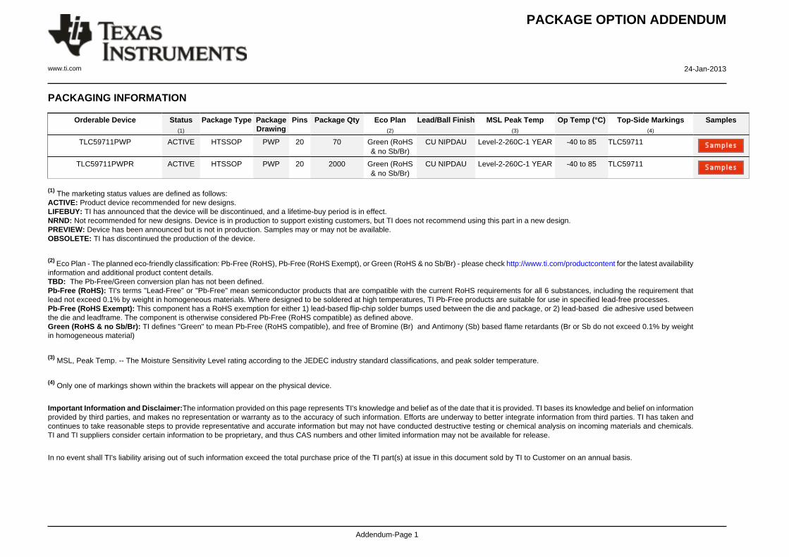
ORDERING INFORMATION (1)
PACKAGE TRANSPORT MEDIA,PRODUCT PACKAGE-LEAD DESIGNATOR ORDERING NUMBER QUANTITY
TLC59711PWPR Tape and Reel, 2000TLC59711 HTSSOP-20 PowerPAD™ PWP
TLC59711PWP Tube, 70
(1) For the most current package and ordering information, see the Package Option Addendum at the end of this document, or visit thedevice product folder at www.ti.com.
2 Copyright © 2011–2012, Texas Instruments Incorporated

TLC59711
www.ti.com SBVS181A –OCTOBER 2011–REVISED JULY 2012
ABSOLUTE MAXIMUM RATINGS (1) (2)
Over operating free-air temperature range, unless otherwise noted.VALUE
UNITMIN MAX
Supply voltage VCC –0.3 +18 V
IREF –0.3 VREG + 0.3 VInput voltage
SDTI, SCKI –0.3 VREG + 0.6 V
OUTR0 to OUTR3, OUTG0 to OUTG3, OUTB0 to OUTB3 –0.3 +18 V
Output voltage SDTO, SCKO –0.3 VREG + 0.3 V
VREG –0.3 +6 V
OUTR0 to OUTR3, OUTG0 to OUTG3, OUTB0 to OUTB3 75 mAOutput current (DC)
VREG –30 mA
Operating junction temperature TJ (max) +150 °C
Storage temperature Tstg –55 +150 °C
Human body model (HBM) 4 kVElectrostatic discharge rating
Charged device model (CDM) 2 kV
(1) Stresses beyond those listed under absolute maximum ratings may cause permanent damage to the device. These are stress ratingsonly, and functional operation of the device at these or any other conditions beyond those indicated under recommended operatingconditions is not implied. Exposure to absolute-maximum-rated conditions for extended periods may affect device reliability.
(2) All voltage values are with respect to network ground terminal.
THERMAL INFORMATIONTLC59711
THERMAL METRIC (1) PWP UNITS
20 PINS
θJA Junction-to-ambient thermal resistance 68.6
θJCtop Junction-to-case (top) thermal resistance 44.2
θJB Junction-to-board thermal resistance 19.3°C/W
ψJT Junction-to-top characterization parameter 2.7
ψJB Junction-to-board characterization parameter 15.7
θJCbot Junction-to-case (bottom) thermal resistance 1.8
(1) For more information about traditional and new thermal metrics, see the IC Package Thermal Metrics application report, SPRA953.
Copyright © 2011–2012, Texas Instruments Incorporated Submit Documentation Feedback 3
Product Folder Link(s): TLC59711

TLC59711
SBVS181A –OCTOBER 2011–REVISED JULY 2012 www.ti.com
RECOMMENDED OPERATING CONDITIONSAt TA = –40°C to +85°C, and VCC = 4 V to 17 V or VCC = VREG = 3.0 V to 5.5 V, unless otherwise noted.
TLC59711UNIT
MIN NOM MAX
DC CHARACTERISTICS
VCC Supply voltage, internal voltage regulator used 4 17 V
VREG Supply voltage, VREG connected to VCC 3 3.3 5.5 V
Voltage applied to outputVO 17 V(OUTR0 to OUTR3, OUTG0 to OUTG3, OUTB0 to OUTB3)
VIH High-level input voltage (SDTI, SCKI) 0.7 × VREG VREG V
VIL Low-level input voltage (SDTI, SCKI) GND 0.3 × VREG V
VIHYS Input voltage hysteresis (SDTI, SCKI) 0.2 × VREG V
IOH High-level output current (SDTO) –2 mA
IOL Low-level output current (SDTO) 2 mA
Constant output sink currentIOLC 60 mA(OUTR0 to OUTR3, OUTG0 to OUTG3, OUTB0 to OUTB3)
IREG Voltage regulator output current (VREG) –25 mA
TA Operating free temperature range –40 +85 °C
TJ Operating junction temperature –40 +125 °C
AC CHARACTERISTICS
fCLK (SCKI) Data clock frequency and GS control clock frequency, SCKI 0.007 10 MHz
tWH/tWL Pulse duration, SCKI 10 ns
tSU Setup time, SDTI – SCKI↑ 5 ns
tH Hold time, SDTI – SCKI↑ 3 ns
ELECTRICAL CHARACTERISTICSAt TA = –40°C to +85°C, VCC = 4 V to 17 V or VCC = VREG = 3 V to 5.5 V, VLED = 5 V, and CVREG = 1 µF, unless otherwisenoted. Typical values are at TA = +25°C and VCC = 12 V.
TLC59711
PARAMETER TEST CONDITIONS MIN TYP MAX UNIT
VOH High-level output voltage, SDTO/SCKO IOH = –2 mA VREG – 0.4 VREG V
VOL Low-level output voltage, SDTO/SCKO IOL = 2 mA 0 0.4 V
VIREF Reference voltage output, IREF RIREF = 0.82 kΩ 1.18 1.21 1.24 V
VREG Linear regulator output voltage, VREG VCC = 4 V to 17 V, IREG = 0 mA to –25 mA 3.1 3.3 3.5 V
ΔVREG Line regulation of linear regulator, VREG VCC = 4 V to 17 V, IREG = 0 mA 90 mV
ΔVREG1 Load regulation of linear regulator, VREG VCC = 12 V, IREG = 0 mA to –25 mA 120 mV
VSTR Undervoltage lockout release, VREG 2.5 2.7 2.9 V
VHYS Undervoltage lockout hysteresis, VREG 300 400 500 mV
II Input current, SDTI/SCKI VI = VREG or GND –1 1 µA
SDTI/SCKI = low, BLANK = 1, GSn = FFFFh,ICC 2 4 mA
BCX = 7Fh, VOUTXn = 1 V, RIREF = 24 kΩ (IOLCMax = 2 mA)
SDTI/SCKI = low, BLANK = 1, GSn = FFFFh,ICC1 6 9 mA
BCX = 7Fh, VOUTXn = 1 V, RIREF = 1.6 kΩ (IOLCMax = 30 mA)
SDTI = 5 MHz, SCKI = 10 MHz, BLANK = 0,Supply currentICC2 auto repeat enable, external GS clock selected, GSn = FFFFh, 10 18 mA
BCX = 7Fh, VOUTXn = 1 V, RIREF = 1.6 kΩ (IOLCMax = 30 mA)
SDTI = 5 MHz, SCKI = 10 MHz, BLANK = 0,ICC3 auto repeat enable, external GS clock selected, GSn = FFFFh, 16 32 mA
BCX = 7Fh, VOUTXn = 1 V, RIREF = 0.82 kΩ (IOLCMax = 60 mA)
All OUTXn on, BCX = 7Fh, VOUTXn = 1 V,IOLC Constant output current, OUTXn 56.3 60.5 64.7 mA
VOUTfix = 1 V, RIREF = 0.82 kΩ (IOLCMax = 60 mA)
All OUTXn off, BCX = 7Fh, VOUTXn = 17 V,IOLKG Leakage output current, OUTXn 0.1 µA
VOUTfix = 17 V, RIREF = 0.82 kΩ (IOLCMax = 60 mA)
4 Submit Documentation Feedback Copyright © 2011–2012, Texas Instruments Incorporated
Product Folder Link(s): TLC59711

100
3 V 1 V-
´
(I at V = 1 V)Xn OUTXnOLC
(I at V = 3 V) (I at V = 1 V)-OLCXn OUTXn OLCXn OUTXnD (%/V) =
100
(I at VCC = 3 V)XnOLC
(I at VCC = 5.5 V) (I at VCC = 3 V)Xn Xn-OLC OLC
5.5 V 3 V-
D (%/V) = ´
I (mA) = 41 ´Xn(IDEAL)OLC
1.21
RIREF ( )W
D (%) =Ideal Output Current
- (Ideal Output Current)(I + I + I + I )X0 X1 X2 X3OLC OLC OLC OLC
4´ 100
D (%) = - 1I XnOLC
(I + I + I + I )X0 X1 X3X2OLC OLC OLC OLC
4
´ 100
TLC59711
www.ti.com SBVS181A –OCTOBER 2011–REVISED JULY 2012
ELECTRICAL CHARACTERISTICS (continued)At TA = –40°C to +85°C, VCC = 4 V to 17 V or VCC = VREG = 3 V to 5.5 V, VLED = 5 V, and CVREG = 1 µF, unless otherwisenoted. Typical values are at TA = +25°C and VCC = 12 V.
TLC59711
PARAMETER TEST CONDITIONS MIN TYP MAX UNIT
Constant-current error (1)
All OUTXn on, BCX = 7Fh, VOUTXn = VOUTfix = 1 V,ΔIOLC (channel-to-channel in same color group), ±1 ±3 %RIREF = 0.82 kΩ (IOLCMax = 60 mA)
OUTXn
Constant current error (2) All OUTXn on, BCX = 7Fh, VOUTXn = VOUTfix = 1V,ΔIOLC1 (device-to-device in same color group), RIREF = 0.82 kΩ (IOLCMax = 60 mA), at same grouped color output ±1 ±4 %
OUTXn of OUTR0-3, OUTG0-3, and OUTB0-3
Line regulation of constant-current output, All OUTn on, BCX = 7Fh, VOUTXn = VOUTfix = 1 V,ΔIOLC2 ±0.5 ±1 %/VOUTXn(3) RIREF = 0.82 kΩ (IOLCMax = 60 mA)
Load regulation of constant-current output, All OUTn on, BCX = 7Fh, VOUTXn = VOUTfix = 1 V,ΔIOLC3 ±1 ±3 %/VOUTXn(4) RIREF = 0.82 kΩ (IOLCMax = 60 mA)
TTSD Thermal shutdown temperature Junction temperature (5) 150 165 180 °C
THYS Thermal shutdown hysteresis Junction temperature(5) 5 10 20 °C
VIREF Reference voltage output, IREF RIREF = 0.82 kΩ 1.18 1.21 1.24 V
VREG Linear regulator output voltage, VREG VCC = 4 V to 17 V, IREG = 0 mA to –25 mA 3.1 3.3 3.5 V
ΔVREG Line regulation of linear regulator, VREG VCC = 4 V to 17 V, IREG = 0 mA 90 mV
ΔVREG1 Load regulation of linear regulator, VREG VCC = 12 V, IREG = 0 mA to –25 mA 120 mV
VSTR Undervoltage lockout release, VREG 2.5 2.7 2.9 V
VHYS Undervoltage lockout hysteresis, VREG 300 400 500 mV
(1) The deviation of each output in the same color group (OUTR0-OUTR3 or OUTG0-OUTG3 or OUTB0-OUTB3) from the average currentfrom the same color group. Deviation is calculated by the formula:
Where: X = R/G/B, and n = 0-3(2) The deviation of each color group constant-current average from the ideal constant-current value.
Deviation is calculated by the following formula:
Where: X = R/G/B.Ideal current is calculated by the following formula for the OUTRn and OUTGn groups:
Where: X = R/G/B.(3) Line regulation is calculated by this equation:
Where: X = R/G/B, n = 0-3.(4) Load regulation is calculated by the equation:
Where: X = R/G/B, n = 0-3.(5) Not tested, specified by design.
Copyright © 2011–2012, Texas Instruments Incorporated Submit Documentation Feedback 5
Product Folder Link(s): TLC59711

TLC59711
SBVS181A –OCTOBER 2011–REVISED JULY 2012 www.ti.com
SWITCHING CHARACTERISTICSAt TA = –40°C to +85°C, VCC = 4 V to 17 V or VCC = VREG = 3 V to 5.5 V, CVREG = 1 µF, CL = 15 pF, RL = 68 Ω, and VLED = 5V, unless otherwise noted. Typical values are at TA = +25°C and VCC = 12 V.
TLC59711
PARAMETER TEST CONDITIONS MIN TYP MAX UNIT
tR0 Rise time, SDTO/SCKO 4 10 15 ns
tR1 Rise time, OUTXn BCX = 7Fh 5 15 ns
tF0 Fall time, SDTO/SCKO 4 10 15 ns
tF1 Fall time, OUTXn BCX = 7Fh 15 25 ns
tD0 Propagation delay SCKI↑ to SDTO↑↓ 44 72 124 ns
tD1 SCKI↑ to SCKO↑, VREG = 3.3 V 11 22 53 ns
tD2(1) SCKO↑ to SDTO↑↓, VREG = 3.3 V 33 50 71 ns
SCKI↑ to OUTRn↑↓, BLANK = 0,BCXn = 7Fh, OUTTMG = 1tD3 10 25 60 nsOr SCKI↓ to OUTRn↑↓, BLANK = 0,BCXn = 7Fh, OUTTMG = 0
SCKI↑ to OUTGn↑↓, BLANK = 0,BCXn = 7Fh, OUTTMG = 1tD4 25 50 90 nsOr SCKI↓ to OUTGn↑↓, BLANK = 0,BCXn = 7Fh, OUTTMG = 0
SCKI↑ to OUTBn↑↓, BLANK = 0,BCXn = 7Fh, OUTTMG = 1tD5 40 75 120 nsOr SCKI↓ to OUTBn↑↓, BLANK = 0,BCXn = 7Fh, OUTTMG = 0
Last SCKI↑ to internal latch pulsetD6(2) 8/fOSC 16384/fOSC secgenaration
tW(SCKO) Shift clock output one pulse width SCKO↑ to SCKO↓ 29 41 70 ns
fOSC Internal oscillator frequency 7 10 12 MHz
(1) The propagation delays are calculated by tD2a = tD0a – tD1a or tD2b = tD0b – tD1b.(2) The generation timing of the internal latch pulse changes depending on the SCKI clock frequency; see the Internal Latch Pulse
Generation Timing section.
6 Submit Documentation Feedback Copyright © 2011–2012, Texas Instruments Incorporated
Product Folder Link(s): TLC59711

Write
Command
Decode
6
218
SDTO
Refe encer
Current
Control
SCKI
IREF
GND
224-Bit Shift Register
218-Bit Data Latch
GS Clock
Counter
SCKO
12-Channel Constant Sink Current Driver
with 7-Bit, 3-Grouped BC
3-Grouped Switching Delay
12
LSB MSB
0 223
LSB MSB
0 217
VCC
SDTI
OUTB3OUTG3OUTR3OUTB0OUTG0OUTR0
26
UVLO
21
Thermal
Detection
Clock
Timing
Adjust
3.3 V
REGVREG
Data
Latch
Control/
Watchdog
Timer
reset
reset
Clock
Select
Internal
Oscillator16-Bit ES-PW Timing ControlM
intlat
1921 intlat
3
16
wrtena
EXTCLK
BLANK
TMGRST
BCX
GSX
BLANK
DSPRPT
OUTTMG
12
2
TLC59711
www.ti.com SBVS181A –OCTOBER 2011–REVISED JULY 2012
FUNCTIONAL BLOCK DIAGRAM
Copyright © 2011–2012, Texas Instruments Incorporated Submit Documentation Feedback 7
Product Folder Link(s): TLC59711

IREF
GND
OUTR0
OUTG0
OUTB0
OUTR1
OUTG1
OUTB1
SDTI
SCKI
VREG
VCC
OUTB3
OUTG3
OUTR3
OUTB2
OUTG2
OUTR2
SDTO
SCKO
1
2
3
4
5
6
7
8
9
10
20
19
18
17
16
15
14
13
12
11
PowerPAD
(Bottom Side)
TLC59711
SBVS181A –OCTOBER 2011–REVISED JULY 2012 www.ti.com
PIN CONFIGURATIONS
PWP PACKAGEHTSSOP-20 PowerPAD
(TOP VIEW)
TERMINAL FUNCTIONSTERMINAL
NAME PWP I/O DESCRIPTION
Maximum current programming terminal.A resistor connected between IREF and GND sets the maximum current for every constant-currentIREF 1 I/O output. When this terminal is directly connected to GND, all outputs are forced off. The external resistorshould be placed close to the device.
GND 2 — Power ground terminal
OUTB0 5 OBLUE constant-current outputs.OUTB1 8 OMultiple outputs can be configured in parallel to increase the constant-current capability.
OUTB2 15 O Different voltages can be applied to each output.OUTB3 18 O
OUTG0 4 OGREEN constant-current outputs.OUTG1 7 OMultiple outputs can be configured in parallel to increase the constant-current capability.
OUTG2 14 O Different voltages can be applied to each output.OUTG3 17 O
OUTR0 3 ORED constant-current outputs.OUTR1 6 OMultiple outputs can be configured in parallel to increase the constant-current capability.
OUTR2 13 O Different voltages can be applied to each output.OUTR3 16 O
Serial data shift clock input.Data present on SDTI are shifted to the LSB of the 224-bit shift register with the SCKI rising edge Data inSCKI 10 I the shift register are shifted toward the MSB at each SCKI rising edge.The MSB data of the shift register appear on SDTO.
Serial data shift clock output.SCKO 11 O The input shift clock signal from SCKI is adjusted to the timing of the serial data output for SDTO and the
signal is then output at SCKO.
SDTI 9 I Serial data input for the 224-bit shift register
Serial data output of the 224-bit shift register.SDTO 12 O SDTO is connected to the MSB of the 224-bit shift register. Data are clocked out at the falling edge
SCKO.
Internal linear voltage regulator output.A decoupling capacitor of 1 µF must be connected. This output can be used for external devices as a 3.3-
VREG 20 I/O V power supply. This terminal can be connected with the VREG terminal of other devices to increase thesupply current. Also, this pin can be supplied with 3 V to 5.5 V from an external power supply byconnecting it to VCC.
VCC 19 — Power-supply terminal
8 Submit Documentation Feedback Copyright © 2011–2012, Texas Instruments Incorporated
Product Folder Link(s): TLC59711

VREG
IREF
GND
VCC
RIREF
CVREG
VCC
VOUTXn
VOUTfix
OUTR0
OUTXn(1)
OUTB3
¼¼
VREG SDTO/SCKO
CL
(1)
GND
VCC
CVREG
VCC
VREG
OUTXn(1)
CL
(2)
RL
IREF
GND
VCC
RIREF
CVREG
VCCVLED
OUTXn(1)
GND
VREG
OUTPUT
GND
VREG
INPUT
GND
TLC59711
www.ti.com SBVS181A –OCTOBER 2011–REVISED JULY 2012
PARAMETRIC MEASUREMENT INFORMATION
PIN EQUIVALENT INPUT/OUTPUT SCHEMATICS
Figure 1. SDTI/SCKIFigure 2. SDTO/SCKO
(1) X = R/G/B, n = 0-3.
Figure 3. OUTR0 Through OUTB3
TEST CIRCUITS
(1) X = R/G/B, n = 0-3.
(2) CL includes measurement probe and stray capacitance.(1) CL includes measurement probe and stray capacitance.
Figure 4. Rise/Fall Time Test Circuit for OUTXnFigure 5. Rise/Fall Time Test Circuit for
SDTO/SCKO
(1) X = R/G/B, n = 0-3.
Figure 6. Constant-Current Test Circuit for OUTXn
Copyright © 2011–2012, Texas Instruments Incorporated Submit Documentation Feedback 9
Product Folder Link(s): TLC59711

t , t , t , t , t , t , t :, t , t , tR0 R1 F0 F1 D0 D1 D2 D3 D4 D5
INPUT(1) 50%
50%
90%
10%
OUTPUT
tD
t or tR F
V or VOL OUTXnL
V or VOH OUTXnH
GND
VREG
T , T :WH WL
SCKI(1)
SCKI(1)
SDTI(1)
T , T :SU H
TSU TH
VREG
VREG
GND
VREG
GND
GND
50%
50%
50%
TWH TWL
TLC59711
SBVS181A –OCTOBER 2011–REVISED JULY 2012 www.ti.com
TIMING DIAGRAMS
(1) Input pulse rise and fall time is 1ns to 3ns.
Figure 7. Input Timing
(1) Input pulse rise and fall time is 1ns to 3ns.
Figure 8. Output Timing
10 Submit Documentation Feedback Copyright © 2011–2012, Texas Instruments Incorporated
Product Folder Link(s): TLC59711

WRT
CMD5
WRT
CMD4
WRT
CMD3
WRT
CMD2
WRT
CMD1
WRT
CMD0
tH
WRT
CMD5
WRT
CMD0
DATA
217B
DATA
1BDATA
0B
DATA
2B
1 2 6tWL
222 223 224 1 2 3 4 5 6 7 8 9
tD6
(2)
tWH
Write Command (6 Bits)
DATA
217C
DATA
216C
DATA
215C
WRT
CMD4
Write Data (218 Bits)
DATA
0A
WRT
CMD5
WRT
CMD4
WRT
CMD0
WRT
CMD5
WRT
CMD1WRT
CMD0
DATA
0A
DATA
217B
DATA
2B
DATA
1B
DATA
0B
DATA
1A
DATA
0A
DATA
3B
DATA
2B
DATA
1B
WRT
CMD5
WRT
CMD4
WRT
CMD3
WRT
CMD5
WRT
CMD4
WRT
CMD3
WRT
CMD5
WRT
CMD4
WRT
CMD2
DATA
217A
DATA
216A
DATA
1A
DATA
0A
DATA
216A
DATA
215A
DATA
0A
WRT
CMD5
WRT
CMD4
WRT
CMD3
WRT
CMD2
WRT
CMD1
WRT
CMD0
DATA
217C
DATA
216C
WRT
CMD5
WRT
CMD4
WRT
CMD3
WRT
CMD2
WRT
CMD1
WRT
CMD0
DATA
217C
WRT
CMD4
WRT
CMD3
WRT
CMD2
WRT
CMD1
WRT
CMD0
DATA
217B
DATA
216B
DATA
215B
WRT
CMD3
WRT
CMD2
WRT
CMD1
WRT
CMD0
DATA
217B
DATA
216B
DATA
215B
DATA
214B
DATA
0B
WRT
CMD5
WRT
CMD4WRT
CMD3
WRT
CMD5
WRT
CMD4
WRT
CMD3
WRT
CMD2
WRT
CMD1
WRT
CMD0
DATA
217B
DATA
216B
DATA
215B
DATA
217ADATA
216A
DATA
1A
DATA
0A
t /tR0 F0
tD0
SDTI
SDTO
SCKI
SCKO
tW(SCKO)
Latch Signal
(Internal)
224-Bit Shift Register
LSB (Internal)
224-Bit Shift Register
LSB + 1 (Internal)
224-Bit Shift Register
MSB 1 (Internal)-
224-Bit Shift Register
MSB (Internal)
Latch Data
(Internal)Previous Data Latest Data (All GS Data are 0001h)
tD1
BLANK Bit in Data Latch
(Internal)
1
0
EXTGCK Bit in Data Latch
(Internal) 0
1
OUTTMG Bit in Data Latch
(Internal) 0
1
tD5
tD4
tD3
OUTR0-R3ON
OFF
tF1(V )OUTXnH
(VOUTXnL
(1))
ON
OFF(V )OUTXnH
(VOUTXnL)(1)
ON
OFF(V )OUTXnH
(VOUTXnL)(1)
tR1
OUTG0-G3
OUTB0-B3
tSU
¼ ¼ ¼ ¼
TLC59711
www.ti.com SBVS181A –OCTOBER 2011–REVISED JULY 2012
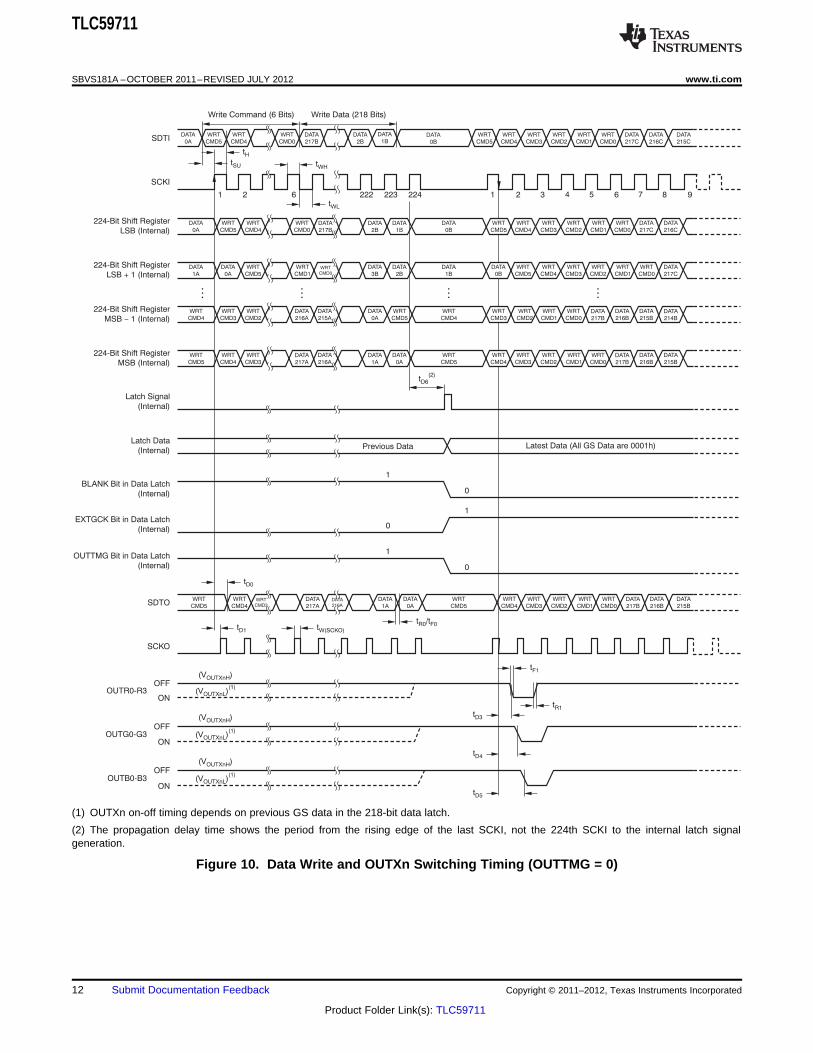
(1) OUTXn on-off timing depends on previous GS data in the 218-bit data latch.
(2) The propagation delay time shows the period from the rising edge of the last SCKI, not the 224th SCKI to the internal latch signalgeneration.
Figure 9. Data Write and OUTXn Switching Timing (OUTTMG = 1)
Copyright © 2011–2012, Texas Instruments Incorporated Submit Documentation Feedback 11
Product Folder Link(s): TLC59711
WRT
CMD5
WRT
CMD4
WRT
CMD3
WRT
CMD2
WRT
CMD1
WRT
CMD0
tH
WRT
CMD5
WRT
CMD0
DATA
217B
DATA
1BDATA
0B
DATA
2B
1 2 6tWL
222 223 224 1 2 3 4 5 6 7 8 9
tD6
(2)
tWH
Write Command (6 Bits)
DATA
217C
DATA
216C
DATA
215C
WRT
CMD4
Write Data (218 Bits)
DATA
0A
WRT
CMD5
WRT
CMD4
WRT
CMD0
WRT
CMD5
WRT
CMD1WRT
CMD0
DATA
0A
DATA
217B
DATA
2B
DATA
1B
DATA
0B
DATA
1A
DATA
0A
DATA
3B
DATA
2B
DATA
1B
WRT
CMD5
WRT
CMD4
WRT
CMD3
WRT
CMD5
WRT
CMD4
WRT
CMD3
WRT
CMD5
WRT
CMD4
WRT
CMD2
DATA
217A
DATA
216A
DATA
1A
DATA
0A
DATA
216A
DATA
215A
DATA
0A
WRT
CMD5
WRT
CMD4
WRT
CMD3
WRT
CMD2
WRT
CMD1
WRT
CMD0
DATA
217C
DATA
216C
WRT
CMD5
WRT
CMD4
WRT
CMD3
WRT
CMD2
WRT
CMD1
WRT
CMD0
DATA
217C
WRT
CMD4
WRT
CMD3
WRT
CMD2
WRT
CMD1
WRT
CMD0
DATA
217B
DATA
216B
DATA
215B
WRT
CMD3
WRT
CMD2
WRT
CMD1
WRT
CMD0
DATA
217B
DATA
216B
DATA
215B
DATA
214B
DATA
0B
WRT
CMD5
WRT
CMD4WRT
CMD3
WRT
CMD5
WRT
CMD4
WRT
CMD3
WRT
CMD2
WRT
CMD1
WRT
CMD0
DATA
217B
DATA
216B
DATA
215B
DATA
217ADATA
216A
DATA
1A
DATA
0A
t /tR0 F0
tD0
SDTI
SDTO
SCKI
SCKO
tW(SCKO)
Latch Signal
(Internal)
224-Bit Shift Register
LSB (Internal)
224-Bit Shift Register
LSB + 1 (Internal)
224-Bit Shift Register
MSB 1 (Internal)-
224-Bit Shift Register
MSB (Internal)
Latch Data
(Internal)Previous Data Latest Data (All GS Data are 0001h)
tD1
BLANK Bit in Data Latch
(Internal)
1
0
EXTGCK Bit in Data Latch
(Internal) 0
1
OUTTMG Bit in Data Latch
(Internal)
tD5
tD4
tD3
OUTR0-R3ON
OFF
tF1(V )OUTXnH
(VOUTXnL
(1))
ON
OFF(V )OUTXnH
(VOUTXnL)(1)
ON
OFF(V )OUTXnH
(VOUTXnL)(1)
tR1
OUTG0-G3
OUTB0-B3
tSU
1
0
¼ ¼¼¼
TLC59711
SBVS181A –OCTOBER 2011–REVISED JULY 2012 www.ti.com
(1) OUTXn on-off timing depends on previous GS data in the 218-bit data latch.
(2) The propagation delay time shows the period from the rising edge of the last SCKI, not the 224th SCKI to the internal latch signalgeneration.
Figure 10. Data Write and OUTXn Switching Timing (OUTTMG = 0)
12 Submit Documentation Feedback Copyright © 2011–2012, Texas Instruments Incorporated
Product Folder Link(s): TLC59711

3
2
1
0
1
2
3
-
-
-
-40 100
Ambient Temperature ( C)°
DI
(%)
OLC
-20 0
I = 60 mA
VCC = 12 V
BCx = 7Fh
OLCMax
20 6040 80
70
60
50
40
30
20
10
00 128
Brightness Control Data (dec)
Ou
tpu
t C
urr
en
t (m
A)
16 32
T = +25
VCC = 12 VA °C
48 8064 11296
I = 60 mAOLCMax
I = 30 mAOLCMax
I = 10 mAOLCMax
I = 2 mAOLCMax
64
63
62
61
60
59
58
57
56
55
540 3
Output Voltage (V)
Outp
ut C
urr
ent (m
A)
0.5 1
I = 60 mA
VCC = 12 V
BCx = 7Fh
OLCMax
1.5 2.52
T = 40 C- °A
T = +25 C°A
T = +85 C°A
3
2
1
0
1
2
3
-
-
-
0 60
Output Current (mA)
DI
(%)
OL
C
10 20
T = +25 C
VCC = 12 V
BCx = 7Fh
°A
30 5040
100
10
1
0.10 70
I , Output Current (mA)OLC
R,
Re
fere
nce
Re
sis
tor
(k)
WIR
EF
10 20 30 5040 60
24.805
9.922
4.9613.307
2.481
1.984
1.654
1.417
1.240
1.102
0.992
0.902
0.827
70
60
50
40
30
20
10
00 3
Output Voltage (V)
Outp
ut C
urr
ent (m
A)
0.5 1
I = 60 mAOLCMax I = 50 mAOLCMax
I = 40 mAOLCMax
I = 30 mAOLCMax
I = 20 mAOLCMax
I = 10 mAOLCMax
T = +25 C, VCC = 12 V, BCx = 7Fh°A
I = 5 mAOLCMaxI = 2 mAOLCMax
1.5 2.52
TLC59711
www.ti.com SBVS181A –OCTOBER 2011–REVISED JULY 2012
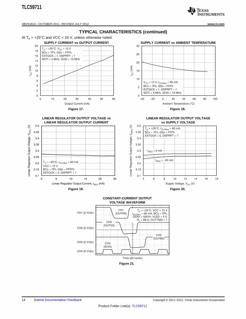
TYPICAL CHARACTERISTICSAt TA = +25°C and VCC = 24 V, unless otherwise noted.
REFERENCE RESISTOR vs OUTPUT CURRENT OUTPUT CURRENT vs OUTPUT VOLTAGE
Figure 11. Figure 12.
CONSTANT-CURRENT ERROR vs OUTPUT CURRENTOUTPUT CURRENT vs OUTPUT VOLTAGE (Channel-to-Channel in Color Group)
Figure 13. Figure 14.
CONSTANT-CURRENT ERROR vsAMBIENT TEMPERATURE
(Channel-to-Channel in Color Group) GLOBAL BRIGHTNESS CONTROL LINEARITY
Figure 15. Figure 16.
Copyright © 2011–2012, Texas Instruments Incorporated Submit Documentation Feedback 13
Product Folder Link(s): TLC59711
Time (20 ns/div)
CH1 (2 V/div)
CH2 (2 V/div)
CH3 (2 V/div)
CH4 (5 V/div)
CH3
(OUTB0)
C 2
(OUTG0)
H
CH1
(OUTR0)T = +25°C,
I = 60 mA, BCx = 7Fh,GSXn = 0001h, VLED = 5 V,
R = 68
VCC = 12 V
W
A
L
OLCMax
, OUTTMG = 1
CH4
(SCKI)
3.5
3.45
3.4
3.35
3.3
3.25
3.2
3.15
3.10 25
Linear Regulator Output Current, I (mA)REG
Lin
ea
r R
eg
ula
tor
Ou
tpu
t V
olta
ge
, V
(V)
RE
G
5 10
T = +25 I = 60 mA,
VCC = 12 V
BCx = 7Fh, GSx = FFFFh
EXTGCK = 0, DSPRPT = 1
A OLCMax°C,
15 20
3.5
3.45
3.4
3.35
3.3
3.25
3.2
3.15
3.14 18
Supply Voltage, V (V)CC
Lin
ea
r R
eg
ula
tor
Ou
tpu
t V
olta
ge
, V
(V)
RE
G
8 10
T = +25 I = 60 mA,
BCx = 7Fh, GSx = FFFh
EXTGCK = 0, DSPRPT = 1
A OLCMax°C,
12 14 16
I = 0 mAREG
I = 25 mA-REG
6
20
18
16
14
12
10
8
6
4
2
00 60
Output Current (mA)
I(m
A)
CC
10 20
T = +25 C, V = 12 V
BCx = 7Fh, GSx = FFFh
EXTGCK = 1, DSPRPT = 1
SDTI = 5 MHz, SCKI = 10 MHz
°A CC
30 5040
30
25
20
15
10
5
0-40 100
Ambient Temperature ( C)°
I(m
A)
CC
-20 0
V = 12 V,
BCx = 7Fh, GSx = FFFh
EXTGCK = 1, DSPRPT = 1
SDTI = 5 MHz, SCKI = 10 MHz
CC I = 60 mAOLCMax
20 6040 80
TLC59711
SBVS181A –OCTOBER 2011–REVISED JULY 2012 www.ti.com
TYPICAL CHARACTERISTICS (continued)At TA = +25°C and VCC = 24 V, unless otherwise noted.
SUPPLY CURRENT vs OUTPUT CURRENT SUPPLY CURRENT vs AMBIENT TEMPERATURE
Figure 17. Figure 18.
LINEAR REGULATOR OUTPUT VOLTAGE vs LINEAR REGULATOR OUTPUT VOLTAGELINEAR REGULATOR OUTPUT CURRENT vs SUPPLY VOLTAGE
Figure 19. Figure 20.
CONSTANT-CURRENT OUTPUTVOLTAGE WAVEFORM
Figure 21.
14 Submit Documentation Feedback Copyright © 2011–2012, Texas Instruments Incorporated
Product Folder Link(s): TLC59711
R (k ) =WIREF
V (V)IREF
I (mA)OLCMax
´ 41
TLC59711
www.ti.com SBVS181A –OCTOBER 2011–REVISED JULY 2012
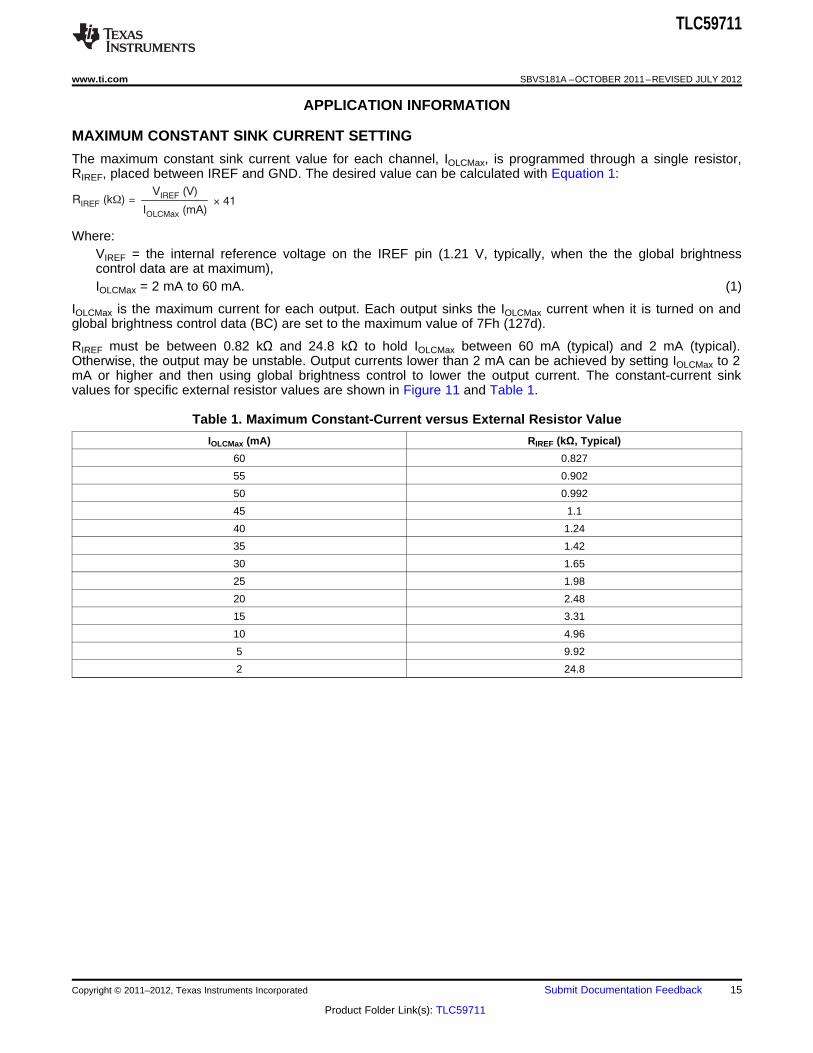
APPLICATION INFORMATION
MAXIMUM CONSTANT SINK CURRENT SETTING
The maximum constant sink current value for each channel, IOLCMax, is programmed through a single resistor,RIREF, placed between IREF and GND. The desired value can be calculated with Equation 1:
Where:VIREF = the internal reference voltage on the IREF pin (1.21 V, typically, when the the global brightnesscontrol data are at maximum),IOLCMax = 2 mA to 60 mA. (1)
IOLCMax is the maximum current for each output. Each output sinks the IOLCMax current when it is turned on andglobal brightness control data (BC) are set to the maximum value of 7Fh (127d).
RIREF must be between 0.82 kΩ and 24.8 kΩ to hold IOLCMax between 60 mA (typical) and 2 mA (typical).Otherwise, the output may be unstable. Output currents lower than 2 mA can be achieved by setting IOLCMax to 2mA or higher and then using global brightness control to lower the output current. The constant-current sinkvalues for specific external resistor values are shown in Figure 11 and Table 1.
Table 1. Maximum Constant-Current versus External Resistor Value
IOLCMax (mA) RIREF (kΩ, Typical)
60 0.827
55 0.902
50 0.992
45 1.1
40 1.24
35 1.42
30 1.65
25 1.98
20 2.48
15 3.31
10 4.96
5 9.92
2 24.8
Copyright © 2011–2012, Texas Instruments Incorporated Submit Documentation Feedback 15
Product Folder Link(s): TLC59711

I I (mA)OUT OLCMax(mA) = ´BCX
127d
TLC59711
SBVS181A –OCTOBER 2011–REVISED JULY 2012 www.ti.com
GLOBAL BRIGHTNESS CONTROL (BC) FUNCTION (SINK CURRENT CONTROL)
The TLC59711 has the capability to adjust all output currents of each color group (OUTR0-3, OUTG0-3, andOUTB0-3) to the same current value. This function is called global brightness (BC) control. The BC data areseven bits long, which allows each color group output current to be adjusted in 128 steps from 0% to 100% ofthe maximum output current, IOLCMax. The BC data are set via the serial interface. When the BC data arechanged, the output current is changed immediately.
When the IC is powered on, all outputs are forced off by BLANK (bit 213). BLANK initializes in the data latch butthe data in the 224-bit shift register and the 218-bit data latch are not set to a default value, except for theBLANK bit. Therefore, BC data must be written to the data latch when BLANK is set to '0'.
Equation 2 determines each color group maximum output sink current:
Where:IOLCMax = the maximum channel current for each channel determined by RIREF
BC = the global brightness control value in the data latch for the specific color group(BCX = 0d to 127d, X = R/G/B) (2)
Table 2 summarizes the BC data value versus the output current ratio and set current value.
Table 2. BC Data versus Current Ratio and Set Current Value
OUTPUT CURRENTBC DATA RATIO TO IOLCMax 60 mA IOLCMax 2 mA IOLCMax
BC DATA (Binary) BC DATA (Decimal) (Hex) (%, Typical) (mA, Typical) (mA, Typical)
000 0000 0 00 0 0 0
000 0001 1 01 0.8 0.47 0.02
000 0010 2 02 1.6 0.94 0.03
— — — — — —
111 1101 125 7D 98.4 59.06 1.97
111 1110 126 7E 99.2 59.53 1.98
111 1111 127 7F 100 60 2
16 Submit Documentation Feedback Copyright © 2011–2012, Texas Instruments Incorporated
Product Folder Link(s): TLC59711

t (ns) = t (ns) GSXnOUT_ON GSCLK ´
TLC59711
www.ti.com SBVS181A –OCTOBER 2011–REVISED JULY 2012
GRAYSCALE (GS) FUNCTION (PWM CONTROL)
The TLC59711 can adjust the brightness of each output channel using the enhanced spectrum pulse widthmodulation (ES-PWM) control scheme. The PWM bit length for each output is 16 bits. The use of the 16-bitlength results in 65536 brightness steps from 0% to 100% brightness.
The PWM operation for all color groups is controlled by a 16-bit grayscale (GS) counter. The GS counterincrements on each rising or falling edge of the external or internal GS reference clock that is selected byOUTTMG (bit 217) and EXTGCK (bit 216) in the data latch. When the external GS clock is selected, the GScounter uses the SCKI clock as the grayscale clock. The GS counter is reset to 0000h and all outputs are forcedoff when BLANK (bit 213) is set to '1' in the data latch and the counter value is held at '0' while BLANK is '1',even if the GS reference clock is toggled in between.
Equation 3 calculates each output (OUTXn) total on-time (tOUT_ON):
Where:tGSCLK = one period of the selected GS reference clock
(internal clock = 100ns typical, external clock = the period of SCKI)GSXn = the programmed GS value for OUTXn (0d to 65535d) (3)
Table 3 summarizes the GS data values versus the output total on-time and duty cycle. When the IC is poweredup, BLANK (bit 213) is set to '1' to force all outputs off; however, the 224-bit shift register and the 218-bit datalatch are not set to default values. Therefore, the GS data must be written to the data latch when BLANK (bit213) is set to '0'.
Table 3. Output Duty Cycle and Total On-Time versus GS Data
GS DATA (decimal) GS DATA (hex) ON-TIME DUTY (%) GS DATA (decimal) GS DATA (hex) ON-TIME DUTY (%)
0 0 0 32768 8000 50.001
1 1 0.002 32769 8001 50.002
2 2 0.003 32770 8002 50.004
3 3 0.005 32771 8003 50.005
— — — — — —
8191 1FFF 12.499 40959 9FFF 62.499
8192 2000 12.5 40960 A000 62.501
8193 2001 12.502 40961 A001 62.502
— — — — — —
16383 3FFF 24.999 49149 BFFF 74.997
16384 4000 25 49150 C000 74.998
16385 4001 25.002 49151 C001 75
— — — — — —
24575 5FFF 37.499 57343 DFFF 87.5
24576 6000 37.501 57344 E000 87.501
24577 6001 37.502 57345 E001 87.503
— — — — — —
32765 7FFD 49.996 65533 FFFD 99.997
32766 7FFE 49.998 65534 FFFE 99.998
32767 7FFF 49.999 65535 FFFF 100
Copyright © 2011–2012, Texas Instruments Incorporated Submit Documentation Feedback 17
Product Folder Link(s): TLC59711
TLC59711
SBVS181A –OCTOBER 2011–REVISED JULY 2012 www.ti.com
ENHANCED SPECTRUM (ES) PWM CONTROL
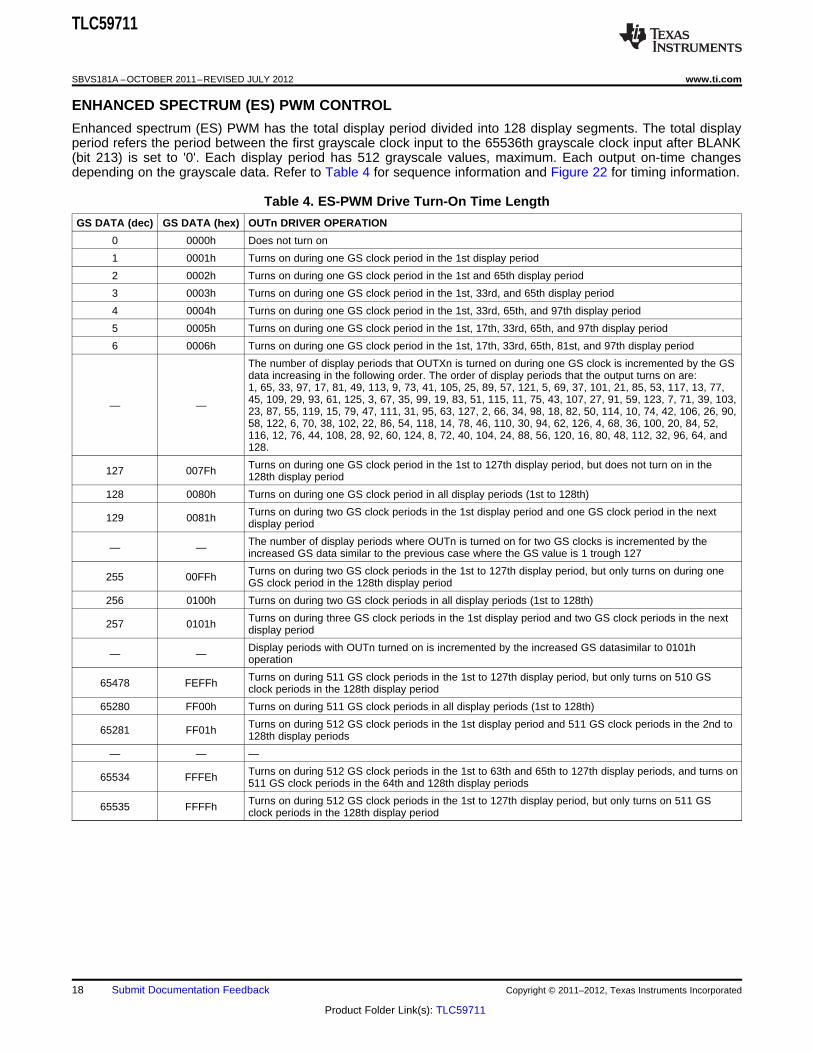
Enhanced spectrum (ES) PWM has the total display period divided into 128 display segments. The total displayperiod refers the period between the first grayscale clock input to the 65536th grayscale clock input after BLANK(bit 213) is set to '0'. Each display period has 512 grayscale values, maximum. Each output on-time changesdepending on the grayscale data. Refer to Table 4 for sequence information and Figure 22 for timing information.
Table 4. ES-PWM Drive Turn-On Time Length
GS DATA (dec) GS DATA (hex) OUTn DRIVER OPERATION
0 0000h Does not turn on
1 0001h Turns on during one GS clock period in the 1st display period
2 0002h Turns on during one GS clock period in the 1st and 65th display period
3 0003h Turns on during one GS clock period in the 1st, 33rd, and 65th display period
4 0004h Turns on during one GS clock period in the 1st, 33rd, 65th, and 97th display period
5 0005h Turns on during one GS clock period in the 1st, 17th, 33rd, 65th, and 97th display period
6 0006h Turns on during one GS clock period in the 1st, 17th, 33rd, 65th, 81st, and 97th display period
The number of display periods that OUTXn is turned on during one GS clock is incremented by the GSdata increasing in the following order. The order of display periods that the output turns on are:1, 65, 33, 97, 17, 81, 49, 113, 9, 73, 41, 105, 25, 89, 57, 121, 5, 69, 37, 101, 21, 85, 53, 117, 13, 77,45, 109, 29, 93, 61, 125, 3, 67, 35, 99, 19, 83, 51, 115, 11, 75, 43, 107, 27, 91, 59, 123, 7, 71, 39, 103,— — 23, 87, 55, 119, 15, 79, 47, 111, 31, 95, 63, 127, 2, 66, 34, 98, 18, 82, 50, 114, 10, 74, 42, 106, 26, 90,58, 122, 6, 70, 38, 102, 22, 86, 54, 118, 14, 78, 46, 110, 30, 94, 62, 126, 4, 68, 36, 100, 20, 84, 52,116, 12, 76, 44, 108, 28, 92, 60, 124, 8, 72, 40, 104, 24, 88, 56, 120, 16, 80, 48, 112, 32, 96, 64, and128.
Turns on during one GS clock period in the 1st to 127th display period, but does not turn on in the127 007Fh 128th display period
128 0080h Turns on during one GS clock period in all display periods (1st to 128th)
Turns on during two GS clock periods in the 1st display period and one GS clock period in the next129 0081h display period
The number of display periods where OUTn is turned on for two GS clocks is incremented by the— — increased GS data similar to the previous case where the GS value is 1 trough 127
Turns on during two GS clock periods in the 1st to 127th display period, but only turns on during one255 00FFh GS clock period in the 128th display period
256 0100h Turns on during two GS clock periods in all display periods (1st to 128th)
Turns on during three GS clock periods in the 1st display period and two GS clock periods in the next257 0101h display period
Display periods with OUTn turned on is incremented by the increased GS datasimilar to 0101h— — operation
Turns on during 511 GS clock periods in the 1st to 127th display period, but only turns on 510 GS65478 FEFFh clock periods in the 128th display period
65280 FF00h Turns on during 511 GS clock periods in all display periods (1st to 128th)
Turns on during 512 GS clock periods in the 1st display period and 511 GS clock periods in the 2nd to65281 FF01h 128th display periods
— — —
Turns on during 512 GS clock periods in the 1st to 63th and 65th to 127th display periods, and turns on65534 FFFEh 511 GS clock periods in the 64th and 128th display periods
Turns on during 512 GS clock periods in the 1st to 127th display period, but only turns on 511 GS65535 FFFFh clock periods in the 128th display period
18 Submit Documentation Feedback Copyright © 2011–2012, Texas Instruments Incorporated
Product Folder Link(s): TLC59711

1 2
128th
Period
65th
Period
96th
Period
65026
65024511 513
3 512
BLANK Bit in Data Latch
(Internal)
ON
OFF
ON
OFF
ON
OFF
16382 16385
16383 16386
514 16384
49150 49153
49151 49154
65023
T =
GS Clock 511d´
1st
Period
97th
Period
127th
PeriodHigh Voltage Level
2nd
Period
32nd
Period
64th
Period
33rd
Period
32766 32769
32767 32770
16387 32768 4915232771
1st
Period
49155 6553665025
65534
65535
OUTXn
(GS Data = 0000h)
OUTXn
(GS Data = 0001h)
OUTXn
(GS Data = 0002h)
ON
OFFOUTXn
(GS Data = 0003h)
ON
OFF
ON
OFF
OUTXn
(GS Data = 0004h)
ON
OFF
OUTXn
(GS Data = 0041h)
OUTXn
(GS Data = 0080h)
ON
OFFOUTXn
(GS Data = 0081h)
ON
OFF
ON
OFF
OUTXn
(GS Data = 0082h)
OUTXn
(GS Data = FF80h)
ON
OFF
ON
OFF
OUTXn
(GS Data = FF81h)
OUTXn
(GS Data = FFFEh)
ON
OFFOUTXn
(GS Data = FFFFh)
GS Reference Clock
(Internal)
When the DSPRPT Bit is ‘1’
T = GS Clock 1d´
T = GS Clock 1d´
T = GS Clock 1d´
T = GS Clock 1d´
T = GS Clock 1d´
T = GS Clock 1d´
T = GS Clock 1d´
T = GS Clock 1d´
T = GS Clock 1d´
T = GS Clock 1d´T = GS Clock 1d´
T = GS Clock 2d´ T = GS Clock 1d´
T = GS Clock 1d´
T = GS Clock 1d´
T = GS Clock 1d´
T = GS Clock 1d´
T = GS Clock 1d´
T = GS Clock 1d´
T = GS Clock 1d´
T = GS Clock 1d´
T = GS Clock 1d´
T = GS Clock 1d´
T = GS Clock 1d´
T = GS Clock 2d´T = GS Clock 1d´
T = GS Clock 2d´
T = GS Clock 1d´
T = GS Clock 1d´T = GS Clock 1d´
T = GSCLK 512d´
T =
GS Clock 512d´
T =
GS Clock 511d´
T =
T =
GS Clock 511d´
T = GS Clock 511d in 2nd to 128th Periods´
T = GS Clock 511d in 2nd to 128th Periods´
T = GS Clock 512d in 2nd to 63rd and 65th to 127th Periods,´
T = GS Clock 511d in 64th Period´
T = GS Clock 512d in 2nd to 127th Periods´
T = GS Clock 1d´
T = GS Clock 1d´
Low Voltage Level
T = GS Clock 1d´
GS Clock 512d´
¼¼
¼¼
¼¼
¼¼
¼ ¼ ¼ ¼
¼ ¼ ¼ ¼
¼
¼ ¼
TLC59711
www.ti.com SBVS181A –OCTOBER 2011–REVISED JULY 2012
Figure 22. ES-PWM Operation
Copyright © 2011–2012, Texas Instruments Incorporated Submit Documentation Feedback 19
Product Folder Link(s): TLC59711
6-Bit Write
Command
Decoder
SDTOSCKI
SDTI
To GS timing control circu t.iTo the three groups of 7-bit BC,
PWM timing control, GS clock counter,
and clock select circuit.
224-Bit Shift Register
LSBMSB
Write
Command
Bit 5
218
Write
Data
Bit 3
218-Bit Data Latch
0123215216217218223
LSB
0123
OUTR0
Bit 3
OUT
TMG
215217
MSB
19226
214
6
Write Command = 25h (100101b)
Inte nalr
Latch Pulse
The internal latch pulse is generated
after eight periods between the last
2 SCKI rising edges with no input.
216 214
EXT
GCK
TMG
RST
DSP
RPT
¼ ¼
¼
Write
Command
Bit 0
Write
Data
Bit 217
Write
Data
Bit 216
Write
Data
Bit 215
Write
Data
Bit 214
Write
Data
Bit 2
Write
Data
Bit 1
Write
Data
Bit 0
OUTR0
Bit 2
OUTR0
Bit 1
OUTR0
Bit 0
TLC59711
SBVS181A –OCTOBER 2011–REVISED JULY 2012 www.ti.com
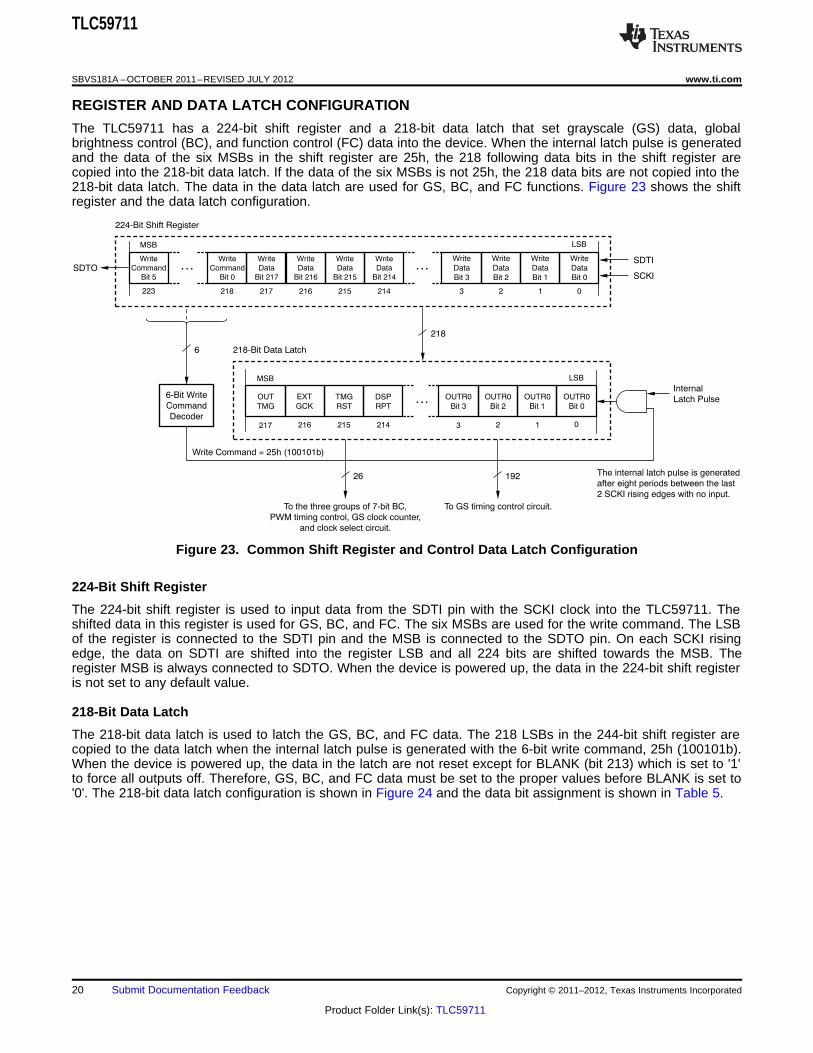
REGISTER AND DATA LATCH CONFIGURATION
The TLC59711 has a 224-bit shift register and a 218-bit data latch that set grayscale (GS) data, globalbrightness control (BC), and function control (FC) data into the device. When the internal latch pulse is generatedand the data of the six MSBs in the shift register are 25h, the 218 following data bits in the shift register arecopied into the 218-bit data latch. If the data of the six MSBs is not 25h, the 218 data bits are not copied into the218-bit data latch. The data in the data latch are used for GS, BC, and FC functions. Figure 23 shows the shiftregister and the data latch configuration.
Figure 23. Common Shift Register and Control Data Latch Configuration
224-Bit Shift Register
The 224-bit shift register is used to input data from the SDTI pin with the SCKI clock into the TLC59711. Theshifted data in this register is used for GS, BC, and FC. The six MSBs are used for the write command. The LSBof the register is connected to the SDTI pin and the MSB is connected to the SDTO pin. On each SCKI risingedge, the data on SDTI are shifted into the register LSB and all 224 bits are shifted towards the MSB. Theregister MSB is always connected to SDTO. When the device is powered up, the data in the 224-bit shift registeris not set to any default value.
218-Bit Data Latch
The 218-bit data latch is used to latch the GS, BC, and FC data. The 218 LSBs in the 244-bit shift register arecopied to the data latch when the internal latch pulse is generated with the 6-bit write command, 25h (100101b).When the device is powered up, the data in the latch are not reset except for BLANK (bit 213) which is set to '1'to force all outputs off. Therefore, GS, BC, and FC data must be set to the proper values before BLANK is set to'0'. The 218-bit data latch configuration is shown in Figure 24 and the data bit assignment is shown in Table 5.
20 Submit Documentation Feedback Copyright © 2011–2012, Texas Instruments Incorporated
Product Folder Link(s): TLC59711

218-Bit Data Latch
21
OUTTMG
1 =
Rising Edge
MSB
217
¼EXTCLK
1 =
External
216
TMGRST
1 =
Reset
215
DSPRPT
1 =
Repeat
214
BLANK
1 =
Blank
213
BC Data
Bits 6-0
for BLUE
212-206
BC Data
Bits 6-0
for GREEN
205-199
BC Data
Bits 6-0
for RED
198-192
OUTB3
Bit 15
191
OUTB3
Bit 0
176
OUTG0
Bit 0
16
OUTR0
Bit 15
15
OUTG0
Bit 15
31
¼ OUTR0
Bit 0¼
LSB
0
218
From LSB-side of 224-bit shift register.
5 192
To function control (FC) circuit. To global brightness control (BC) circuit. To grayscale timing control (GS) circuit.
Function Control Data (5 Bits) BC Data for OUTRn/Gn/Bn
(7 Bits 3 = 21 Bits)´
¼
GS Data for OUTG0
(16 Bits)
GS Data for OUTB3
(16 Bits)
GS Data for OUTR0
(16 Bits)
TLC59711
www.ti.com SBVS181A –OCTOBER 2011–REVISED JULY 2012
Figure 24. 218-Bit Data Latch Configuration
Table 5. Data Latch Bit Assignment
BIT NUMBER BIT NAME CONTROLLED CHANNEL/FUNCTIONS
15-0 GSR0 GS data bits 15 to 0 for OUTR0
31-16 GSG0 GS data bits 15 to 0 for OUTG0
47-32 GSB0 GS data bits 15 to 0 for OUTB0
63-48 GSR1 GS data bits 15 to 0 for OUTR1
79-64 GSG1 GS data bits 15 to 0 for OUTG1
95-80 GSB1 GS data bits 15 to 0 for OUTB1
111-96 GSR2 GS data bits 15 to 0 for OUTR2
127-112 GSG2 GS data bits 15 to 0 for OUTG2
143-128 GSB2 GS data bits 15 to 0 for OUTB2
159-144 GSR3 GS data bits 15 to 0 for OUTR3
175-160 GSG3 GS data bits 15 to 0 for OUTG3
191-176 GSB3 GS data bits 15 to 0 for OUTB3
198-192 BCR BC data bits 6 to 0 for OUTR0-3
205-199 BCG BC data bits 6 to 0 for OUTG0-3
212-206 BCB BC data bits 6 to 0 for OUTB0-3
Constant-current output enable bit in FC data (0 = output control enabled, 1 = blank).When this bit is '0', all constant-current outputs (OUTR0-OUTB3) are controlled by the GS PWM timing213 BLANK controller. When this bit is '1', all constant-current outputs are forced off. The GS counter is reset to '0',and the GS PWM timing controller is initialized. When the IC is powered on, this bit is set to '1'.
Auto display repeat mode enable bit in FC data (0 = disabled, 1 = enabled).When this bit is '0', the auto repeat function is disabled. Each constant-current output is only turned on
214 DSPRPT once, according the GS data after BLANK is set to '0' or after the internal latch pulse is generated withthe TMGRST bit set to '1'. When this bit is '1', each output turns on and off according to the GS dataevery 65536 GS reference clocks.
Display timing reset mode enable bit in FC data (0 = disabled, 1 = enabled).When this bit is '1', the GS counter is reset to '0' and all constant-current outputs are forced off whenthe internal latch pulse is generated for data latching. This function is the same when BLANK is set to215 TMGRST '0'. Therefore, BLANK does not need to be controlled by an external controller when this mode isenabled. When this bit is '0', the GS counter is not reset and no output is forced off even if the internallatch pulse is generated.
GS reference clock select bit in FC data (0 = internal oscillator clock, 1 = SCKI clock).216 EXTGCK When this bit is '1', PWM timing refers to the SCKI clock. When this bit is '0', PWM timing refers to the
internal oscillator clock.
GS reference clock edge select bit for OUTXn on-off timing control in FC data (0 = falling edge, 1 =rising edge).217 OUTTMG When this bit is '1', OUTXn are turned on or off at the rising edge of the selected GS reference clock.When this bit is '0', OUTXn are turned on or off at the falling edge of the selected clock.
Copyright © 2011–2012, Texas Instruments Incorporated Submit Documentation Feedback 21
Product Folder Link(s): TLC59711

12
3
GS Reference Clock(SCKI or Internal Oscillator)
OUTXn(GSDATA = FFFFh)
OUTn is forced offwhen BLANK is ‘1’.
Display period is repeatedby auto refresh function.
OFF
ON
OUTn is not turnedon until the nextBLANK changes
to ‘0’.
DSPRPT = 0(Auto Repeat Off)
BLANK Bitin Data Latch
(Internal)
DSPRPT Bitin Data Latch
(Internal)
2nd Display Period 3rd Display Period1st Display Period
1stDisplay Period
45
65533
6553465535
65536
12
3
45
65533
6553465535
65536
12
3
45
6
78
9
10 1 655342 65535
65536
12
DSPRPT = 1(Auto Repeat On)
218-bit data are copied from shift register
when the internal latch is generated.
N 3-
SCKI
1
Latch Pulse
(Internal)
Period A
The internal latch pulse is generated when the SCKI rising edge is not input during 8 times of
Period A if the 6-bit data of the MSB-side in the 244-bit shift register is the command code .25h
The next SCKI clock should start after 8 or more
clock periods (1.34 s, min) of the internal clock
from the internal latch pulse generation timing.
m
224-Bit Shift
Register Data
(Internal)
218-Bit
Data Latch
(Internal)
Write command 25h + 218-bit data.
N 2- N 1- N2 3 4 ¼
TLC59711
SBVS181A –OCTOBER 2011–REVISED JULY 2012 www.ti.com
INTERNAL LATCH PULSE GENERATION TIMING
The internal latch pulse is generated when the SCKI rising edge does not change for 8x the period between thelast SCKI rising edge and the second to last SCKI rising edge if the data of the six MSBs in the 244-bit shiftregister are the command code 25h. The generation timing changes as a result of the SCKI frequency with thetime range between 16384 times the internal oscillator period (2.74ms), maximum, and 8x the internal oscillatorperiod (666 ns), minimum. Figure 25 shows the internal latch pulse generation timing.
Figure 25. Data Latch Pulse Generation Timing
AUTO DISPLAY REPEAT FUNCTION
This function repeats the total display period without a BLANK bit change, as long as the GS reference clock isavailable. This function can be enabled or disabled with DSPRPT (bit 214) in the data latch. When the DSPRPTbit is '1', this function is enabled and the entire display period repeats without a BLANK bit data change. Whenthe DSPRPT bit is '0', this function is disabled and the entire display period executes only once after the BLANKbit is set to '0' or the internal latch pulse is generated when the display timing reset function is enabled. Figure 26shows the auto display repeat operation timing.
Figure 26. Auto Repeat Display Function
22 Submit Documentation Feedback Copyright © 2011–2012, Texas Instruments Incorporated
Product Folder Link(s): TLC59711

SCKI
N 4-
OUTXn
OUTTMG Bit
in
(Internal)
Data Latch
1
TMGRST Bit
in Data Latch
(Internal)
0 = No BLANK.
1 = OUTXn on-off state is changed at the rising edge of the clock selected by the EXTCLK bit.
BLANK Bit
in Data Latch
(Internal)
1 = Display timing reset function is enabled.
OFF
ON
EXTCLK Bit
in
(Internal)
Data Latch
1 = OUTXn on-off state is changed at the rising edge of the clock selected by the EXTCLK bit.
Internal Latch Pulse
(Internal)
Period A
OFF
ONON
GS Counter
for PWM Control
(Internal)
0MM-1M-2M-3M 4- 1
When the TMGRST bit is ‘1’, the GS counter is
reset to ‘0’ at the internal latch pulse generation timing.
Also, OUTXn is forced off at the same time.
2 3
N 3- N 2- N 1- N
8x Period A8x or greater internal
clock period
(1.34 s, min).m
2 3 ¼
TLC59711
www.ti.com SBVS181A –OCTOBER 2011–REVISED JULY 2012
DISPLAY TIMING RESET FUNCTION
This function allows the display timing to be initialized using the internal latch pulse, as shown in Figure 27. Thisfunction can be enabled or disabled by TMGRST (bit 215) in the data latch. When the TMGRST bit is '1', the GScounter is reset to '0' and all outputs are forced off when the internal latch pulse is generated. This function is thesame when the BLANK bit changes (such as from '0' to '1' and from '1' to '0'). Therefore, the BLANK bit does notneed to be controlled from an external controller to restart the PWM control from the next GS reference clockrising edge. When this bit is '0', the GS counter is not reset and no output is forced off even if the internal latchpulse is generated. Figure 27 shows the display timing reset operation.
Figure 27. Display Timing Reset Function
OUTPUT TIMING SELECT FUNCTION
This function selects the on-off change timing of the constant-current outputs (OUTXn) set by OUTTMG (bit 217)in the data latch. When this bit is '1', OUTXn are turned on or off at the rising edge of the selected GS referenceclock. When this bit is '0', OUTXn are turned on or off at the falling edge of the selected clock. Electromagneticinterference (EMI) of the total system can be reduced using this bit setting. For example, when the odd numberof devices in the system have this bit set to '0' and the even number of devices in the system have this bit set to'1', EMI is reduced because the devices change the OUTXn status at a deferent timing. Figure 28 and Figure 29show the output switching timing when the OUTTMG bit is '1' and '0', respectively.
Copyright © 2011–2012, Texas Instruments Incorporated Submit Documentation Feedback 23
Product Folder Link(s): TLC59711

tD3
tD5
tD4
SCKI
1
OUTR0-R3
OUTTMG Bit
in Data Latch
(Internal)
65534
EXTCLK Bit
in Data Latch
(Internal)
1
0
0 = OUTXn on-off state changes at the falling edge of the clock selected by the EXTCLK bit.
BLANK Bit
in Data Latch
(Internal)
1 = SCKI used for OUTXn on-off timing control.
OUTG0-G3
OUTB0-B3
OUTXn on-off state changes at the falling
edge of the clock selected by the EXTCLK bit.
OFF
OFF
OFF
ON
ON
ONtD3
tD5
tD4
2 655353 65536¼
tD3
tD5
tD4
SCKI
1
OUTR0-R3
OUTTMG Bit
in Data Latch
(Internal)
65534
EXTCLK Bit
in Data Latch
(Internal)
1
0
1 = OUTXn on-off state changes at the rising edge of the clock selected by the EXTCLK bit.
BLANK Bit
in Data Latch
(Internal)
1 = SCKI used for OUTXn on-off timing control.
OUTG0-G3
OUTB0-B3
OUTXn on-off state changes at the rising
edge of the clock selected by the EXTCLK bit.
OFF
OFF
OFF
ON
ON
ON
2 3 65535 65536¼
tD3
tD5
tD4
TLC59711
SBVS181A –OCTOBER 2011–REVISED JULY 2012 www.ti.com
Figure 28. Output On-Off Timing with Four-Channel Grouped Delay (OUTTMG = 1)
Figure 29. Output On-Off Timing with Four-Channel Grouped Delay (OUTTMG = 0)
24 Submit Documentation Feedback Copyright © 2011–2012, Texas Instruments Incorporated
Product Folder Link(s): TLC59711

SCKI
1 = SCKI is used for OUTXn on-off timing control.
OFF
OFF
OFF
ON
ON
ON
OUTG0-G3
OUTB0-B3
BLANK Bit
in Data Latch
(Internal)
EXTCLK Bit
in Data Latch
(Internal)
OUTTMG Bit
in Data Latch
(Internal)
1
0
1 = OUTXn on-off state is changed at the rising edge of the clock selected by the EXTCLK bit.
1 2
The watchdog forces all OUTXn off when SCKI stops at a high
level or low level, regardless of the shift register data.
¼Period A 8x Period A
TLC59711
www.ti.com SBVS181A –OCTOBER 2011–REVISED JULY 2012
WATCHDOG TIMER FUNCTION
This function is enabled when SCKI clock is selected as GS reference clock by EXTGCK (bit 216) in the datalatch. When EXTGCK bit is '1', if SCKI rising edge does not change for 8x the period between the last SCKIrising edge and the second to last SCKI rising edge with any accident, all OUTXn is forced off and GS clockcounter is reset to “0” to avoid displaying unexpected image.
Figure 31 shows the watchdog operation timing when SCKI rising edge is not changed with EXTGCK bit is ‘1’.
Figure 30. Watchdog Operation Timing with no SCKI Clock Input (OUTTMG = 1)
THERMAL SHUTDOWN
The thermal shutdown (TSD) function turns off all IC constant-current outputs when the junction temperature (TJ)exceeds the threshold (TTSD = +165°C, typ). When the junction temperature drops below (TTSD – THYS), theoutput control starts at the first GS clock in the next display period.
NOISE REDUCTION
Large surge currents may flow through the IC and the board if all 12 outputs turn on simultaneously at the start ofeach GS cycle. These large current surges could induce detrimental noise and EMI into other circuits. TheTLC59711 turns on the outputs for each color group independently with a 25 ns (typ) rise time. The outputcurrent sinks are grouped into three groups. The first group that is turned on/off are OUTR0-3; the second groupthat is turned on/off are OUTG0-3; and the third group is OUTB0-3. However, the state of each output iscontrolled by the selected GS clock; see the Output Timing Select Function section.
Copyright © 2011–2012, Texas Instruments Incorporated Submit Documentation Feedback 25
Product Folder Link(s): TLC59711

VCC
SDTI
SCKI
IREF
GND
SDTO
SCKO
VREF
1st
TLC59711
VLED
DATA
CLK
GND
Controller
¼
3.3 V
VCC
SDTI
SCKI
IREF
GND
SDTO
SCKO
VREF
2nd
TLC59711
¼
VCC
SDTI
SCKI
IREF
GND
SDTO
SCKO
VREF
N 1st-
TLC59711
¼
VCC
SDTI
SCKI
IREF
GND
SDTO
SCKO
VREF
Nth
TLC59711
¼
MSB
Write
Command
(6 bits, 25h)
Function
Control
(5 bits)
BC for
BLUE
(7 bits)
BC for
GREEN
(7 bits)
BC for
RED
(7 Bits)
GS for
OUTB3
(16 Bits)
GS for
OUTG3
(16 Bits)
GS for
OUTR3
(16 Bits)
16 Bits
6´
GS for
OUTB0
(16 Bits)
GS for
OUTG0
(16 Bits)
GS for
OUTR0
(16 Bits)
LSB
TLC59711
SBVS181A –OCTOBER 2011–REVISED JULY 2012 www.ti.com
HOW TO CONTROL THE TLC59711
To set each function mode, BC color, GS output, 6-bit write command, 5-bit FC data, 21-bit BC data for eachcolor group, and 192-bit GS data for OUTXn, a total number of 224 bits must be written into the device.Figure 31 shows the 224-bit data packet configuration.
When N units of the TLC59711 are cascaded (as shown in Figure 32), N × 224 bits must be written from thecontroller into the first device to control all devices. The number of cascaded devices is not limited as long as theproper voltage is supplied to the device at VCC. The packets for all devices must be written again whenever thedata in one packet is changed.
Figure 31. 224-Bit Data Packet Configuration
Figure 32. Cascading Connection of N TLC59711 Units
26 Submit Documentation Feedback Copyright © 2011–2012, Texas Instruments Incorporated
Product Folder Link(s): TLC59711

for
N-2’th
Shift Data From
Controller (SDTI)
Shift Clock From
Controller (SCKI)
OUTXn
VLED Power
224 Shift Clocks
224-Bit Packet
for Nth TLC59711
MSB
224 Shift Clocks
224-Bit Packet
for N 1st- TLC59711
for
3’rd
224-Bit Packet
for 2nd TLC59711
224-Bit Packet
for 1st TLC59711
Next
Data
Next
Shift Clock
PWM Control Start
or data updated
The time that generates the internal latch pulse is 8x the period between the last
SCLK rising edge and the second to last SCLK rising edge. The time changes
depending on the period of the shift clock within the range of 2.74 ms to 666 ns.
The next shift clock should start after 1.34 s
or more from the internal latch pulse generation timing.
m
Latch Pulse
(Internal)
MSB
MSB
MSB
MSB
MSB
LSB
LSB
LSB
LSB
LSB
224 Shift Clocks 224 Shift Clocks
TLC59711
www.ti.com SBVS181A –OCTOBER 2011–REVISED JULY 2012
Data Write and PWM Control with Internal Grayscale Clock Mode
When the EXTCLK bit is '0', the internal oscillator clock is used for PWM control of OUTXn (X = R/G/B and n = 0-3) as the GS reference clock. This mode is ideal for illumination applications that change the display image atlow frequencies. The data and clock timing is shown in Figure 9 and Figure 33. A writing procedure for thefunction setting and display control follows:1. Power up VCC (VLED); all OUTXn are off because BLANK is set to '1'.2. Write the 224-bit data packet (with MSB bit first) for the Nth TLC59711 using the SDTI and SCKI signals.
The first six bits of the 224-bit data packet are used as the write command. The write command must be 25h(100101b); otherwise, the 218-bit data in the 224-bit shift register are not copied to the 218-bit data latch.The EXTCLK bit must be set to '0' for the internal oscillator mode. Also, the DSPRPT bit should be set to '1'to repeat the PWM timing control and BLANK set to '0' to start the PWM control.
3. Write the 224-bit data packet for the (N – 1) TLC59711 without delay after step 2.4. Repeat the data write sequence until all TLC59711s have data. The total shift clock count (SCKI) is now 224
× N. After all device data are written, stop the SCKI at a high or low level for 8× the period between the lastSCKI rising edge and the second to last SCKI rising edge. Then the 218 LSBs in the 224-bit shift resister arecopied to the 218-bit data latch in all devices and the PWM control is started or updated at the same time.
Figure 33. Data Packet and Display Start/Update Timing 1 (Internal Oscillator Mode)
Copyright © 2011–2012, Texas Instruments Incorporated Submit Documentation Feedback 27
Product Folder Link(s): TLC59711

for
2nd
for
N 1st-
Shift Data From
Controller (SDTI)
Shift Clock From
Controller (SCKI)
OUTXn
VLED Power
224 Shift Clocks
224-Bit Packet
for Nth TLC59711
65536 Shift Clocks as GS Clock
224-Bit Packet
for 1st TLC59711
OUTXn is controlled via the PWM
synchronized with SCKI.
The time that generates the internal latch pulse is 8x the period between the last
SCLK rising edge and the second to last SCLK rising edge. The time changes
depending on the period of the shift clock within the range of 2.74 ms to 666 ns.
The next shift clock should start after 1.34 s
or more from the internal latch pulse generation timing.
m
Low
Latch Pulse
(Internal)
224-Bit Packet
for Nth TLC59711
MSB LSB
MSB LSB
MSB LSB MSB
224 Shift Clocks224 Shift
Clocks
TLC59711
SBVS181A –OCTOBER 2011–REVISED JULY 2012 www.ti.com
Data Write and PWM Control with External Grayscale Clock Mode
When the EXTCLK bit is '1', the data shift clock (SCKI) is used for PWM control of OUTXn (X = R/G/B and n = 0-3) as the GS reference clock. This mode is ideal for video image applications that change the display image withhigh frequencies or for certain display applications that must synchronize all TLC59711s. The data and clocktiming are shown in Figure 9 and Figure 34. A writing procedure for the display data and display timing controlfollows:1. Power- up VCC (VLED); all OUTXn are off because BLANK is set to '1'.2. Write the 224-bit data packet MSB-first for the Nth TLC59711 using the SDTI and SCKI signals. The first six
bits of the 224-bit data packet are used as the write command. The write command must be 25h (100101b);otherwise, the 218-bit data in the 224-bit shift register are not copied to the 218-bit data latch. The EXTCLKbit must be set to '1' for the external oscillator mode. Also, the DSPRPT bit should be set to '0' so that thePWM control is not repeated, the TMGRST bit should be set to '1' to reset the PWM control timing at theinternal latch pulse generation, and BLANK must be set to '0' to start the PWM control.
3. Write the 224-bit data for the (N – 1) TLC59711 without delay after step 2.4. Repeat the data write sequence until all TLC59711s have data. The total shift clock count (SCKI) is 224 × N.
After all device data are written, stop the SCKI at a high or low level for 8× the period between the last SCKIrising edge and the second to last SCKI rising edge. Then the 218 LSBs in the 224-bit shift resister arecopied to the 218-bit data latch in all devices.
5. To start the PWM control, send one pulse of the SCKI clock with SDTI low after 1.34µs or more from step 4.The OUTXn are turned on when the output GS data are not 0000h.
6. Send the remaining 65535 SCKI clocks with SDTI low. Then the PWM control for OUTXn is synchronizedwith the SCKI clock and one display period is finished with a total of 65536 SCKI clock periods.
7. Repeat step 2 to step 6 for the next display period.
Figure 34. Data Packet and Display Start/Update Timing 2 (External Clock Mode)
28 Submit Documentation Feedback Copyright © 2011–2012, Texas Instruments Incorporated
Product Folder Link(s): TLC59711

Timing clock for 1st display and
2nd display data write.
Shift Clock
for 2nd Display
for
2nd
LSB
for
255th
Shift Data From
Controller (SDTI)
Shift Clock From
Controller (SCKI)
OUTXn
VLED Power
224 Shift Clocks
224-Bit Packet for
256th TLC59711
8192
Shift Clocks
MSB
224-Bit Packet
for 1st TLC59711
OUTXn is controlled via the PWM synchronized
with SCKI for 1st displayperiod.
The time is 8 periods between the last SCLK rising edge and the second to last SCLK rising edge.
The wait time changes between 2.74 ms and 666 ns, depending on the period of the shift clock.
The next shift clock should start after 1.34 s or more from the internal latch pulse generation timing.m
256 224-Bit Packet for
256th TLC59711
´
Low
57344 (256 224)
Shift Clocks
´
Latch Pulse
(Internal)
Low
OFF OFF2nd Display
Period
Timing clock for 1st display.MSB LSB MSB LSB
224 Shift Clocks
224 256 = 57344 Clocks´ 65536 Clocks 65536 Clocks
TLC59711
www.ti.com SBVS181A –OCTOBER 2011–REVISED JULY 2012
There is another control procedure that is recommended for a long chain of cascaded devices. The data andclock timings are shown in Figure 9 and Figure 35. When 256 TLC59711 units are cascaded, use the followingprocedure:1. Power up VCC (VLED); all OUTXn are off because BLANK is set to '1'.2. Write the 224-bit data packet MSB-first for the 256th TLC59711 using the SDTI and SCKI signals. The
EXTCLK bit must be set to '1' for the external oscillator mode. Also, the DSPRPT bit should be set to '0' sothat the PWM control does not repeat, the TMGRST bit should be set to '1' to reset the PWM control timingwith the internal latch pulse, and BLANK must be set to '0' to start the PWM control.
3. Repeat the data write sequence for all TLC59711s. The total shift clock count (SCKI) is 57344 (224 × 256).After all device data are written, stop the SCKI signal at a high or low level for eight or more periods betweenthe last SCKI rising edge and the second to last SCKI rising edge. Then the 218 LSBs in the 224-bit shiftresister are copied to the 218-bit data latch in all devices.
4. To control the PWM, send 8192 SCKI clock periods with SDTI low after 1.34µs or more from step 3 (or step7). These 8192 clock periods are used for the OUTXn PWM control.
5. Write the new 224-bit data packets to the 256th to first TLC59711s for the next display with 256 × 224 SCKIclock for a total of 57344 clocks. The PWM control for OUTXn remains synchronized with the SCKI clock andone display period is finished with a total of 65536 SCKI clocks. The SCKI clock signal is therefore used forPWM control and, at the same time, to write data into the shift registers of all cascaded parts.
6. Stop the SCKI signal at a high or low level for eight or more periods between the last SCKI rising edge andthe second to last SCKI rising edge. Then the 218-bit LSBs in the 224-bit shift resister are copied to the 218-bit data latch in all devices.
7. Repeat step 4 to step 6 for the next display periods.
Figure 35. Data Packet and Display Start/Update Timing 3(External Clock Mode with 256 Cascaded Devices)
Copyright © 2011–2012, Texas Instruments Incorporated Submit Documentation Feedback 29
Product Folder Link(s): TLC59711
TLC59711
SBVS181A –OCTOBER 2011–REVISED JULY 2012 www.ti.com
REVISION HISTORY
NOTE: Page numbers for previous revision may differ from the page numbers in the current version.
Changes from Original (October 2011) to Revision A Page
• Fixed typo in last row of Table 5 ......................................................................................................................................... 21
• Changed Figure 26 ............................................................................................................................................................. 22
30 Submit Documentation Feedback Copyright © 2011–2012, Texas Instruments Incorporated
Product Folder Link(s): TLC59711
PACKAGE OPTION ADDENDUM
www.ti.com 24-Jan-2013
Addendum-Page 1
PACKAGING INFORMATION
Orderable Device Status(1)
Package Type PackageDrawing
Pins Package Qty Eco Plan(2)
Lead/Ball Finish MSL Peak Temp(3)
Op Temp (°C) Top-Side Markings(4)
Samples
TLC59711PWP ACTIVE HTSSOP PWP 20 70 Green (RoHS& no Sb/Br)
CU NIPDAU Level-2-260C-1 YEAR -40 to 85 TLC59711
TLC59711PWPR ACTIVE HTSSOP PWP 20 2000 Green (RoHS& no Sb/Br)
CU NIPDAU Level-2-260C-1 YEAR -40 to 85 TLC59711
(1) The marketing status values are defined as follows:ACTIVE: Product device recommended for new designs.LIFEBUY: TI has announced that the device will be discontinued, and a lifetime-buy period is in effect.NRND: Not recommended for new designs. Device is in production to support existing customers, but TI does not recommend using this part in a new design.PREVIEW: Device has been announced but is not in production. Samples may or may not be available.OBSOLETE: TI has discontinued the production of the device.
(2) Eco Plan - The planned eco-friendly classification: Pb-Free (RoHS), Pb-Free (RoHS Exempt), or Green (RoHS & no Sb/Br) - please check http://www.ti.com/productcontent for the latest availabilityinformation and additional product content details.TBD: The Pb-Free/Green conversion plan has not been defined.Pb-Free (RoHS): TI's terms "Lead-Free" or "Pb-Free" mean semiconductor products that are compatible with the current RoHS requirements for all 6 substances, including the requirement thatlead not exceed 0.1% by weight in homogeneous materials. Where designed to be soldered at high temperatures, TI Pb-Free products are suitable for use in specified lead-free processes.Pb-Free (RoHS Exempt): This component has a RoHS exemption for either 1) lead-based flip-chip solder bumps used between the die and package, or 2) lead-based die adhesive used betweenthe die and leadframe. The component is otherwise considered Pb-Free (RoHS compatible) as defined above.Green (RoHS & no Sb/Br): TI defines "Green" to mean Pb-Free (RoHS compatible), and free of Bromine (Br) and Antimony (Sb) based flame retardants (Br or Sb do not exceed 0.1% by weightin homogeneous material)
(3) MSL, Peak Temp. -- The Moisture Sensitivity Level rating according to the JEDEC industry standard classifications, and peak solder temperature.
(4) Only one of markings shown within the brackets will appear on the physical device.
Important Information and Disclaimer:The information provided on this page represents TI's knowledge and belief as of the date that it is provided. TI bases its knowledge and belief on informationprovided by third parties, and makes no representation or warranty as to the accuracy of such information. Efforts are underway to better integrate information from third parties. TI has taken andcontinues to take reasonable steps to provide representative and accurate information but may not have conducted destructive testing or chemical analysis on incoming materials and chemicals.TI and TI suppliers consider certain information to be proprietary, and thus CAS numbers and other limited information may not be available for release.
In no event shall TI's liability arising out of such information exceed the total purchase price of the TI part(s) at issue in this document sold by TI to Customer on an annual basis.


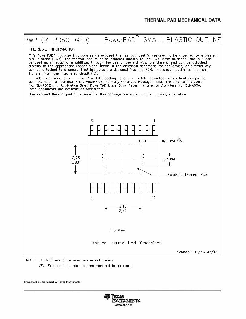

IMPORTANT NOTICE
Texas Instruments Incorporated and its subsidiaries (TI) reserve the right to make corrections, enhancements, improvements and otherchanges to its semiconductor products and services per JESD46, latest issue, and to discontinue any product or service per JESD48, latestissue. Buyers should obtain the latest relevant information before placing orders and should verify that such information is current andcomplete. All semiconductor products (also referred to herein as “components”) are sold subject to TI’s terms and conditions of salesupplied at the time of order acknowledgment.
TI warrants performance of its components to the specifications applicable at the time of sale, in accordance with the warranty in TI’s termsand conditions of sale of semiconductor products. Testing and other quality control techniques are used to the extent TI deems necessaryto support this warranty. Except where mandated by applicable law, testing of all parameters of each component is not necessarilyperformed.
TI assumes no liability for applications assistance or the design of Buyers’ products. Buyers are responsible for their products andapplications using TI components. To minimize the risks associated with Buyers’ products and applications, Buyers should provideadequate design and operating safeguards.
TI does not warrant or represent that any license, either express or implied, is granted under any patent right, copyright, mask work right, orother intellectual property right relating to any combination, machine, or process in which TI components or services are used. Informationpublished by TI regarding third-party products or services does not constitute a license to use such products or services or a warranty orendorsement thereof. Use of such information may require a license from a third party under the patents or other intellectual property of thethird party, or a license from TI under the patents or other intellectual property of TI.
Reproduction of significant portions of TI information in TI data books or data sheets is permissible only if reproduction is without alterationand is accompanied by all associated warranties, conditions, limitations, and notices. TI is not responsible or liable for such altereddocumentation. Information of third parties may be subject to additional restrictions.
Resale of TI components or services with statements different from or beyond the parameters stated by TI for that component or servicevoids all express and any implied warranties for the associated TI component or service and is an unfair and deceptive business practice.TI is not responsible or liable for any such statements.
Buyer acknowledges and agrees that it is solely responsible for compliance with all legal, regulatory and safety-related requirementsconcerning its products, and any use of TI components in its applications, notwithstanding any applications-related information or supportthat may be provided by TI. Buyer represents and agrees that it has all the necessary expertise to create and implement safeguards whichanticipate dangerous consequences of failures, monitor failures and their consequences, lessen the likelihood of failures that might causeharm and take appropriate remedial actions. Buyer will fully indemnify TI and its representatives against any damages arising out of the useof any TI components in safety-critical applications.
In some cases, TI components may be promoted specifically to facilitate safety-related applications. With such components, TI’s goal is tohelp enable customers to design and create their own end-product solutions that meet applicable functional safety standards andrequirements. Nonetheless, such components are subject to these terms.
No TI components are authorized for use in FDA Class III (or similar life-critical medical equipment) unless authorized officers of the partieshave executed a special agreement specifically governing such use.
Only those TI components which TI has specifically designated as military grade or “enhanced plastic” are designed and intended for use inmilitary/aerospace applications or environments. Buyer acknowledges and agrees that any military or aerospace use of TI componentswhich have not been so designated is solely at the Buyer's risk, and that Buyer is solely responsible for compliance with all legal andregulatory requirements in connection with such use.
TI has specifically designated certain components as meeting ISO/TS16949 requirements, mainly for automotive use. In any case of use ofnon-designated products, TI will not be responsible for any failure to meet ISO/TS16949.
Products Applications
Audio www.ti.com/audio Automotive and Transportation www.ti.com/automotive
Amplifiers amplifier.ti.com Communications and Telecom www.ti.com/communications
Data Converters dataconverter.ti.com Computers and Peripherals www.ti.com/computers
DLP® Products www.dlp.com Consumer Electronics www.ti.com/consumer-apps
DSP dsp.ti.com Energy and Lighting www.ti.com/energy
Clocks and Timers www.ti.com/clocks Industrial www.ti.com/industrial
Interface interface.ti.com Medical www.ti.com/medical
Logic logic.ti.com Security www.ti.com/security
Power Mgmt power.ti.com Space, Avionics and Defense www.ti.com/space-avionics-defense
Microcontrollers microcontroller.ti.com Video and Imaging www.ti.com/video
RFID www.ti-rfid.com
OMAP Applications Processors www.ti.com/omap TI E2E Community e2e.ti.com
Wireless Connectivity www.ti.com/wirelessconnectivity
Mailing Address: Texas Instruments, Post Office Box 655303, Dallas, Texas 75265Copyright © 2013, Texas Instruments Incorporated