12-bit,octal, ultralow glitch, voltage … · vouth voutg vfbg vfbf voutf voute vfbe rhb package...
TRANSCRIPT
www.ti.com
FEATURES DESCRIPTION
APPLICATIONS
InputRegister
InputRegister
DACRegister
DACRegister
StringDAC A
StringDAC H
InterfaceLogic
Power-OnReset
Power-DownLogic
+
IOVDD VREF2
SCLK
SYNC
SDIN
VOUTA
VOUTHSDO
RST RSTSEL AGND DGND VREF3 VREF4 PD
−
VFBA
+
−
VFBH
VREF1VDD
DCEN
DAC7558
SLAS435A–MAY 2005–REVISED DECEMBER 2005
12-BIT, OCTAL, ULTRALOW GLITCH, VOLTAGE OUTPUTDIGITAL-TO-ANALOG CONVERTER
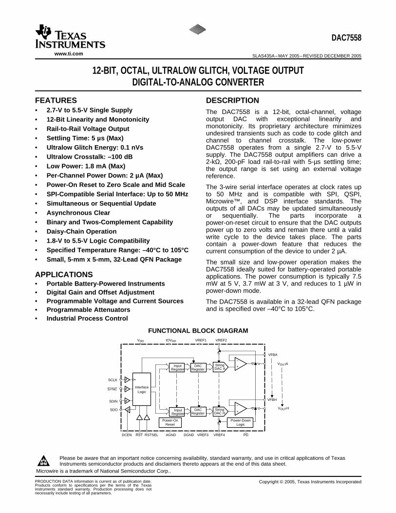
• 2.7-V to 5.5-V Single Supply The DAC7558 is a 12-bit, octal-channel, voltageoutput DAC with exceptional linearity and• 12-Bit Linearity and Monotonicitymonotonicity. Its proprietary architecture minimizes• Rail-to-Rail Voltage Outputundesired transients such as code to code glitch and
• Settling Time: 5 µs (Max) channel to channel crosstalk. The low-power• Ultralow Glitch Energy: 0.1 nVs DAC7558 operates from a single 2.7-V to 5.5-V
supply. The DAC7558 output amplifiers can drive a• Ultralow Crosstalk: –100 dB2-kΩ, 200-pF load rail-to-rail with 5-µs settling time;
• Low Power: 1.8 mA (Max) the output range is set using an external voltage• Per-Channel Power Down: 2 µA (Max) reference.• Power-On Reset to Zero Scale and Mid Scale The 3-wire serial interface operates at clock rates up• SPI-Compatible Serial Interface: Up to 50 MHz to 50 MHz and is compatible with SPI, QSPI,
Microwire™, and DSP interface standards. The• Simultaneous or Sequential Updateoutputs of all DACs may be updated simultaneously
• Asynchronous Clear or sequentially. The parts incorporate a• Binary and Twos-Complement Capability power-on-reset circuit to ensure that the DAC outputs
power up to zero volts and remain there until a valid• Daisy-Chain Operationwrite cycle to the device takes place. The parts• 1.8-V to 5.5-V Logic Compatibility contain a power-down feature that reduces the
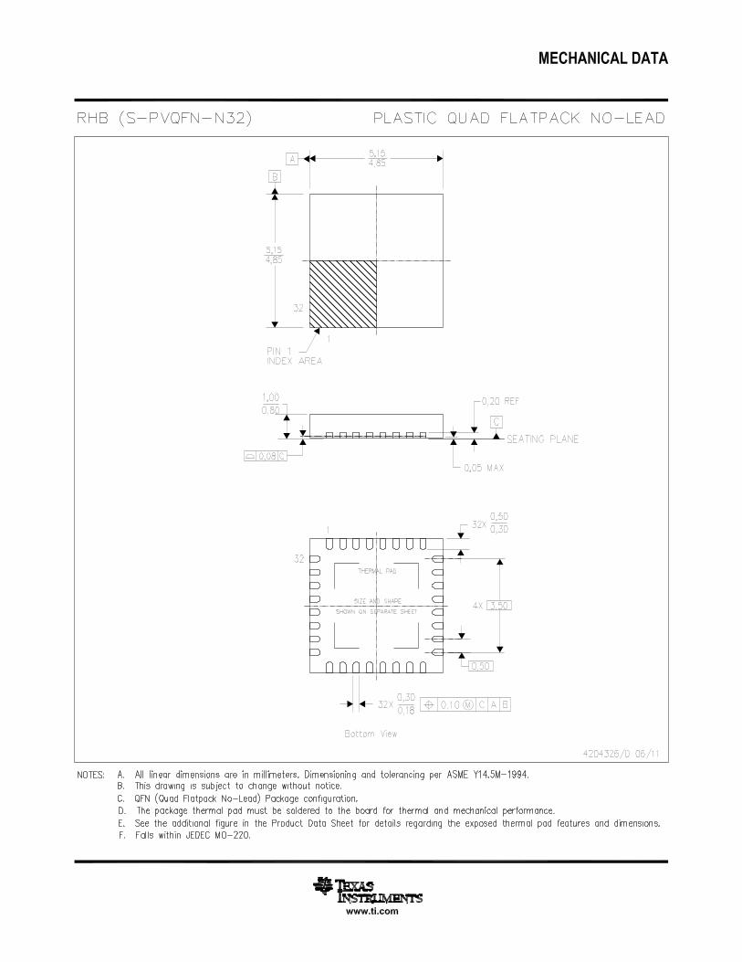
• Specified Temperature Range: –40°C to 105°C current consumption of the device to under 2 µA.• Small, 5-mm x 5-mm, 32-Lead QFN Package The small size and low-power operation makes the
DAC7558 ideally suited for battery-operated portableapplications. The power consumption is typically 7.5mW at 5 V, 3.7 mW at 3 V, and reduces to 1 µW in• Portable Battery-Powered Instrumentspower-down mode.• Digital Gain and Offset Adjustment
• Programmable Voltage and Current Sources The DAC7558 is available in a 32-lead QFN packageand is specified over –40°C to 105°C.• Programmable Attenuators
• Industrial Process Control
FUNCTIONAL BLOCK DIAGRAM
Please be aware that an important notice concerning availability, standard warranty, and use in critical applications of TexasInstruments semiconductor products and disclaimers thereto appears at the end of this data sheet.
Microwire is a trademark of National Semiconductor Corp..
PRODUCTION DATA information is current as of publication date. Copyright © 2005, Texas Instruments IncorporatedProducts conform to specifications per the terms of the TexasInstruments standard warranty. Production processing does notnecessarily include testing of all parameters.

www.ti.com
ABSOLUTE MAXIMUM RATINGS
DAC7558
SLAS435A–MAY 2005–REVISED DECEMBER 2005
This integrated circuit can be damaged by ESD. Texas Instruments recommends that all integratedcircuits be handled with appropriate precautions. Failure to observe proper handling and installationprocedures can cause damage.
ESD damage can range from subtle performance degradation to complete device failure. Precisionintegrated circuits may be more susceptible to damage because very small parametric changes couldcause the device not to meet its published specifications.
ORDERING INFORMATION (1)
SPECIFIEDPACKAGE PACKAGE ORDERING TRANSPORTPRODUCT PACKAGE TEMPERATUREDESIGNATOR MARKING NUMBER MEDIARANGE
DAC7558IRHBT 250-piece Tape andReel
DAC7558 32 QFN RHB –40°C TO 105°C D758DAC7558IRHBR 3000-piece Tape
and Reel
(1) For the most current package and ordering information, see the Package Option Addendum at the end of this document, or see the TIWeb site at www.ti.com.
over operating free-air temperature range (unless otherwise noted) (1)
UNIT
VDD , IOVDD to GND –0.3 V to 6 V
Digital input voltage to GND –0.3 V to VDD + 0.3 V
Vout to GND –0.3 V to VDD+ 0.3 V
Operating temperature range –40°C to 105°C
Storage temperature range –65°C to 150°C
Junction temperature (TJ Max) 150°C
(1) Stresses above those listed under “Absolute Maximum Ratings” may cause permanent damage to the device. Exposure to absolutemaximum conditions for extended periods may affect device reliability.
2

www.ti.com
ELECTRICAL CHARACTERISTICS
DAC7558
SLAS435A–MAY 2005–REVISED DECEMBER 2005
VDD = 2.7 V to 5.5 V, VREF = VDD, RL = 2 kΩ to GND; CL = 200 pF to GND; all specifications –40°C to 105°C, unlessotherwise specified
PARAMETER TEST CONDITIONS MIN TYP MAX UNITS
STATIC PERFORMANCE (1)
Resolution 12 Bits
Relative accuracy ±0.35 ±1 LSB
Differential nonlinearity Specified monotonic by design ±0.08 ±0.5 LSB
Offset error ±12 mV
Zero-scale error All zeroes loaded to DAC register ±12 mV
Gain error VDD = 5 V, VREF = 4.096 V ±0.15 %FSR
Full-scale error VDD = 5 V, VREF = 4.096 V ±0.5 %FSR
Zero-scale error drift 7 µV/°C
Gain temperature coefficient 3 ppm of FSR/°C
PSRR VDD = 5 V 0.75 mV/V
OUTPUT CHARACTERISTICS (2)
Output voltage range 0 VREF V
Output voltage settling time RL = 2 kΩ; 0 pF < CL < 200 pF 5 µs
Slew rate 1.8 V/µs
Capacitive load stability RL = ∞ 470 pF
RL = 2 kΩ 1000
Digital-to-analog glitch impulse 1 LSB change around major carry 0.1 nV-s
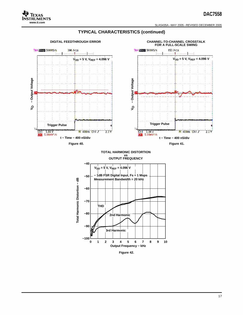
Channel-to-channel crosstalk 1-kHz full-scale sine wave, –100 dBoutputs unloaded
Digital feedthrough 0.1 nV-s
Output noise density (10-kHz offset 120 nV/rtHzfrequency)
Total harmonic distortion FOUT = 1 kHz, FS = 1 MSPS, BW = 20 –85 dBkHz
DC output impedance 1 Ω
Short-circuit current VDD = 5 V 50 mA
VDD = 3 V 20
Power-up time Coming out of power-down mode, 15 µsVDD = 5 V
Coming out of power-down mode, 15VDD = 3 V
REFERENCE INPUT
VREF Input range 0 VDD V
Reference input impedance VREF1 through VREF4 shorted together 12.5 kΩ
Reference current VREF = VDD = 5 V, 400 650 µAVREF1 through VREF4 shorted together
VREF = VDD = 3 V, 240 425VREF1 through VREF4 shorted together
LOGIC INPUTS (2)
Input current ±1 µA
VIN_L, Input low voltage IOVDD ≥ 2.7 V 0.3 IOVDD V
VIN_H, Input high voltage IOVDD ≥ 2.7 V 0.7 IOVDD V
Pin capacitance 3 pF
(1) Linearity tested using a reduced code range of 30 to 4065; output unloaded.(2) Specified by design and characterization, not production tested. For 1.8 V < IOVDD < 2.7 V, it is recommended that VIH = IOVDD , VIL =
GND.
3
www.ti.com
ELECTRICAL CHARACTERISTICS (Continued)
DAC7558
SLAS435A–MAY 2005–REVISED DECEMBER 2005
VDD = 2.7 V to 5.5 V, VREF = VDD, RL = 2 kΩ to GND; CL = 200 pF to GND; all specifications –40°C to 105°C, unlessotherwise specified
PARAMETER TEST CONDITIONS MIN TYP MAX UNITS
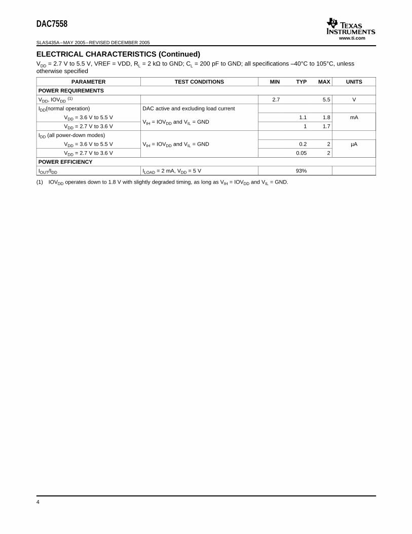
POWER REQUIREMENTS
VDD, IOVDD(1) 2.7 5.5 V
IDD(normal operation) DAC active and excluding load current
VDD = 3.6 V to 5.5 V 1.1 1.8 mAVIH = IOVDD and VIL = GND
VDD = 2.7 V to 3.6 V 1 1.7
IDD (all power-down modes)
VDD = 3.6 V to 5.5 V VIH = IOVDD and VIL = GND 0.2 2 µA
VDD = 2.7 V to 3.6 V 0.05 2
POWER EFFICIENCY
IOUT/IDD ILOAD = 2 mA, VDD = 5 V 93%
(1) IOVDD operates down to 1.8 V with slightly degraded timing, as long as VIH = IOVDD and VIL = GND.
4
www.ti.com
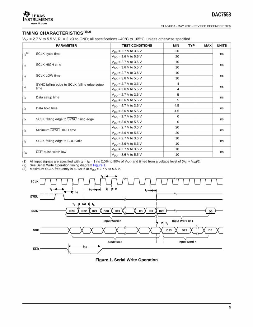
TIMING CHARACTERISTICS (1) (2)
SCLK
SYNC
SDIN D23 D22 D21 D20 D19 D1 D0 D23
t8t4
t3 t2
t1
t7
t6t5
D0
t9Input Word n Input Word n+1
Undefined
D23 D22 D0
Input Word n
t10
SDO
CLR
DAC7558
SLAS435A–MAY 2005–REVISED DECEMBER 2005
VDD = 2.7 V to 5.5 V, RL = 2 kΩ to GND; all specifications –40°C to 105°C, unless otherwise specified
PARAMETER TEST CONDITIONS MIN TYP MAX UNITS
VDD = 2.7 V to 3.6 V 20t1(3) SCLK cycle time ns
VDD = 3.6 V to 5.5 V 20
VDD = 2.7 V to 3.6 V 10t2 SCLK HIGH time ns
VDD = 3.6 V to 5.5 V 10
VDD = 2.7 V to 3.6 V 10t3 SCLK LOW time ns
VDD = 3.6 V to 5.5 V 10
VDD = 2.7 V to 3.6 V 4SYNC falling edge to SCLK falling edge setupt4 nstime VDD = 3.6 V to 5.5 V 4
VDD = 2.7 V to 3.6 V 5t5 Data setup time ns
VDD = 3.6 V to 5.5 V 5
VDD = 2.7 V to 3.6 V 4.5t6 Data hold time ns
VDD = 3.6 V to 5.5 V 4.5
VDD = 2.7 V to 3.6 V 0t7 SCLK falling edge to SYNC rising edge ns
VDD = 3.6 V to 5.5 V 0
VDD = 2.7 V to 3.6 V 20t8 Minimum SYNC HIGH time ns
VDD = 3.6 V to 5.5 V 20
VDD = 2.7 V to 3.6 V 10t9 SCLK falling edge to SDO valid ns
VDD = 3.6 V to 5.5 V 10
VDD = 2.7 V to 3.6 V 10t10 CLR pulse width low ns
VDD = 3.6 V to 5.5 V 10
(1) All input signals are specified with tR = tF = 1 ns (10% to 90% of VDD) and timed from a voltage level of (VIL + VIH)/2.(2) See Serial Write Operation timing diagram Figure 1.(3) Maximum SCLK frequency is 50 MHz at VDD = 2.7 V to 5.5 V.
Figure 1. Serial Write Operation
5
www.ti.com
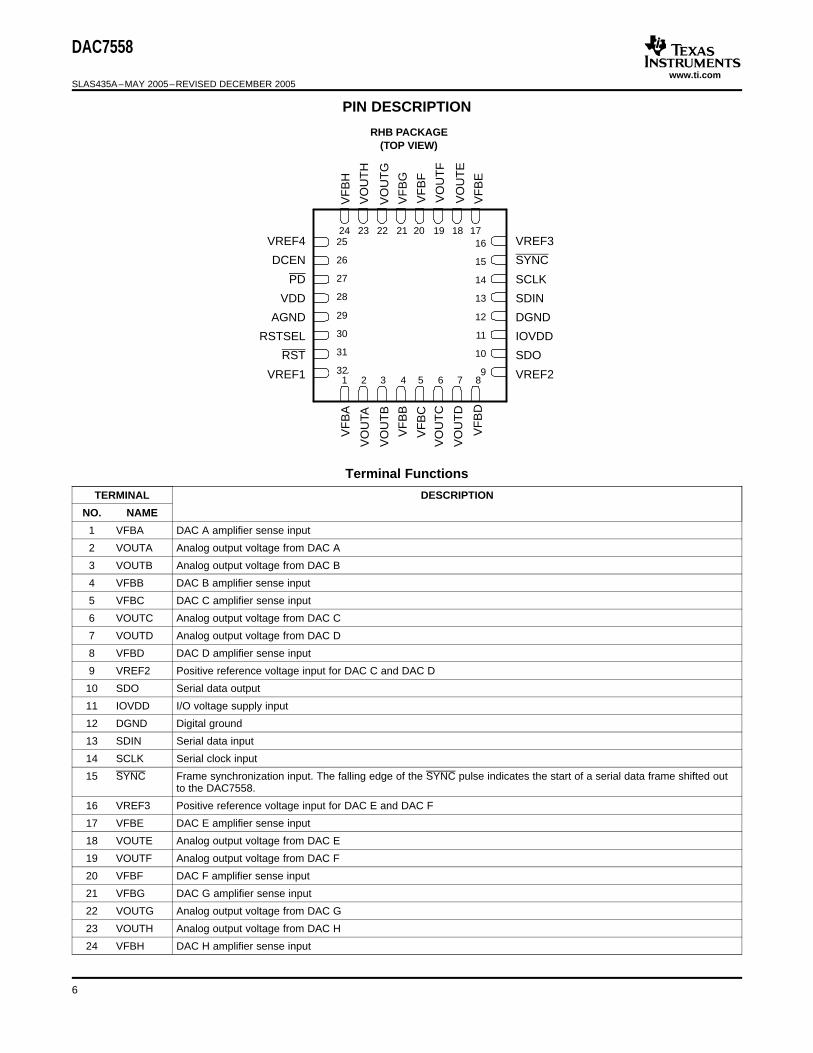
PIN DESCRIPTION
25
26
27
28
29
30
31
321 2 3 4 5 6 7 8
16
15
14
13
12
11
10
9
24 23 22 21 20 19 18 17VREF4
DCEN
PD
VDD
AGND
RSTSEL
RST
VREF1
VREF3
SYNC
SCLK
SDIN
DGND
IOVDD
SDO
VREF2
VF
BH
VF
BA
VO
UTA
VO
UT
B
VF
BB
VF
BC
VO
UT
C
VO
UT
D
VF
BD
VO
UT
H
VO
UT
G
VF
BG
VF
BF
VO
UT
F
VO
UT
E
VF
BE
RHB PACKAGE(TOP VIEW)
DAC7558
SLAS435A–MAY 2005–REVISED DECEMBER 2005
Terminal Functions
TERMINAL DESCRIPTION
NO. NAME
1 VFBA DAC A amplifier sense input
2 VOUTA Analog output voltage from DAC A
3 VOUTB Analog output voltage from DAC B
4 VFBB DAC B amplifier sense input
5 VFBC DAC C amplifier sense input
6 VOUTC Analog output voltage from DAC C
7 VOUTD Analog output voltage from DAC D
8 VFBD DAC D amplifier sense input
9 VREF2 Positive reference voltage input for DAC C and DAC D
10 SDO Serial data output
11 IOVDD I/O voltage supply input
12 DGND Digital ground
13 SDIN Serial data input
14 SCLK Serial clock input
15 SYNC Frame synchronization input. The falling edge of the SYNC pulse indicates the start of a serial data frame shifted outto the DAC7558.
16 VREF3 Positive reference voltage input for DAC E and DAC F
17 VFBE DAC E amplifier sense input
18 VOUTE Analog output voltage from DAC E
19 VOUTF Analog output voltage from DAC F
20 VFBF DAC F amplifier sense input
21 VFBG DAC G amplifier sense input
22 VOUTG Analog output voltage from DAC G
23 VOUTH Analog output voltage from DAC H
24 VFBH DAC H amplifier sense input
6

www.ti.com
TYPICAL CHARACTERISTICS
−1
−0.5
0
0.5
1
Lin
eari
ty E
rro
r −
LS
B
−0.5
−0.25
0
0.25
0.5
0 512 1024 1536 2048 2560 3072 3584 4096
Digital Input Code
Dif
fere
nti
al L
inea
rity
Err
or
− L
SB
Channel A VREF = 4.096 V VDD = 5 V
−1
−0.5
0
0.5
1
−0.5
−0.25
0
0.25
0.5
0 512 1024 1536 2048 2560 3072 3584 4096
Digital Input Code
Lin
eari
ty E
rro
r −
LS
BD
iffe
ren
tial
Lin
eari
ty E
rro
r −
LS
B
Channel B VREF = 4.096 V VDD = 5 V
DAC7558
SLAS435A–MAY 2005–REVISED DECEMBER 2005
PIN DESCRIPTION (continued)
Terminal Functions (continued)
25 VREF4 Positive reference voltage input for DAC G and DAC H
26 DCEN Daisy-chain enable
27 PD Power down
28 VDD Analog voltage supply input
29 AGND (1) Analog ground
30 RSTSEL Reset select. If this pin is low, input coding is binary; if high, then 2s compliment.
31 RST Asynchronous reset. Active low. If RST pin is low, all DAC channels reset either to zero scale (RSTSEL = 0) or tomidscale (RSTSEL = 1).
32 VREF1 Positive reference voltage input for DAC A and DAC B
(1) Thermal pad should be connected to AGND.
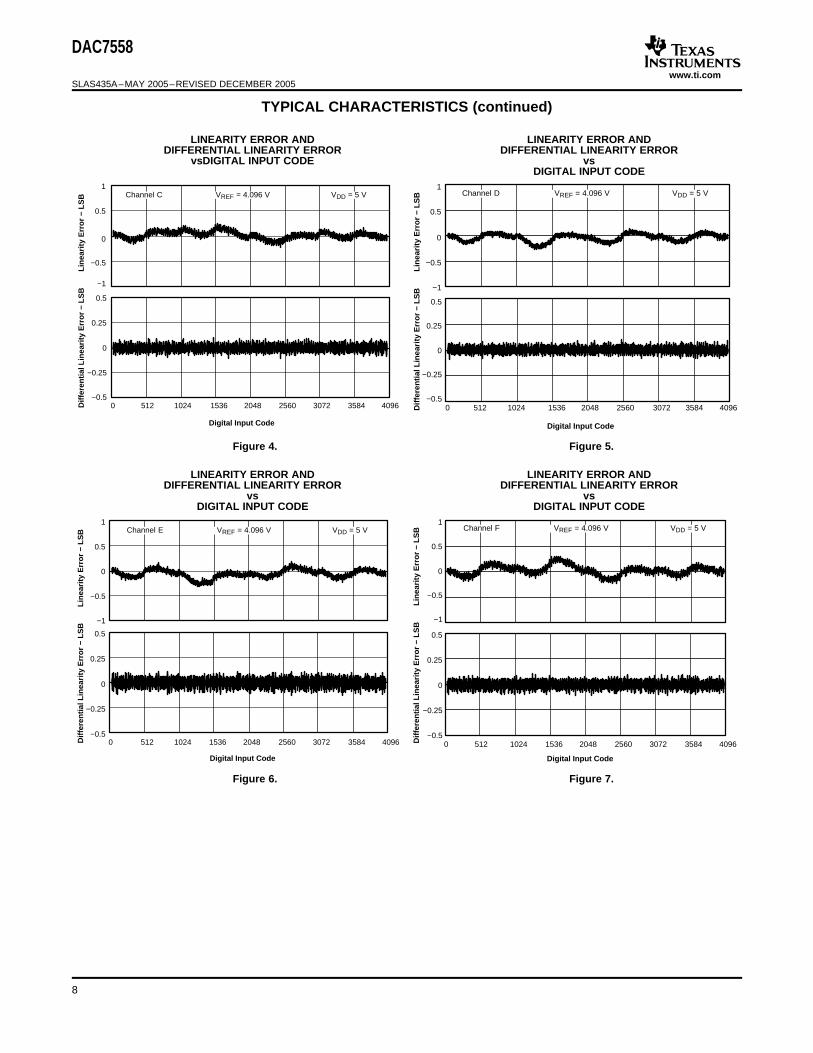
LINEARITY ERROR AND LINEARITY ERROR ANDDIFFERENTIAL LINEARITY ERROR DIFFERENTIAL LINEARITY ERROR
vs vsDIGITAL INPUT CODE DIGITAL INPUT CODE
Figure 2. Figure 3.
7
www.ti.com
−1
−0.5
0
0.5
1
−0.5
−0.25
0
0.25
0.5
0 512 1024 1536 2048 2560 3072 3584 4096
Digital Input Code
Lin
eari
ty E
rro
r −
LS
BD
iffe
ren
tial
Lin
eari
ty E
rro
r −
LS
B
Channel C VREF = 4.096 V VDD = 5 V
−1
−0.5
0
0.5
1
−0.5
−0.25
0
0.25
0.5
0 512 1024 1536 2048 2560 3072 3584 4096
Digital Input CodeL
inea
rity
Err
or
− L
SB
Dif
fere
nti
al L
inea
rity
Err
or
− L
SB
Channel D VREF = 4.096 V VDD = 5 V
−1
−0.5
0
0.5
1
−0.5
−0.25
0
0.25
0.5
0 512 1024 1536 2048 2560 3072 3584 4096
Digital Input Code
Lin
eari
ty E
rro
r −
LS
BD
iffe
ren
tial
Lin
eari
ty E
rro
r −
LS
B
Channel E VREF = 4.096 V VDD = 5 V
−1
−0.5
0
0.5
1
−0.5
−0.25
0
0.25
0.5
0 512 1024 1536 2048 2560 3072 3584 4096
Digital Input Code
Lin
eari
ty E
rro
r −
LS
BD
iffe
ren
tial
Lin
eari
ty E
rro
r −
LS
B
Channel F VREF = 4.096 V VDD = 5 V
DAC7558
SLAS435A–MAY 2005–REVISED DECEMBER 2005
TYPICAL CHARACTERISTICS (continued)
LINEARITY ERROR AND LINEARITY ERROR ANDDIFFERENTIAL LINEARITY ERROR DIFFERENTIAL LINEARITY ERROR
vsDIGITAL INPUT CODE vsDIGITAL INPUT CODE
Figure 4. Figure 5.
LINEARITY ERROR AND LINEARITY ERROR ANDDIFFERENTIAL LINEARITY ERROR DIFFERENTIAL LINEARITY ERROR
vs vsDIGITAL INPUT CODE DIGITAL INPUT CODE
Figure 6. Figure 7.
8

www.ti.com
−1
−0.5
0
0.5
1
−0.5
−0.25
0
0.25
0.5
0 512 1024 1536 2048 2560 3072 3584 4096
Digital Input CodeL
inea
rity
Err
or
− L
SB
Dif
fere
nti
al L
inea
rity
Err
or
− L
SB
Channel H VREF = 4.096 V VDD = 5 V
−1
−0.5
0
0.5
1
−0.5
−0.25
0
0.25
0.5
0 512 1024 1536 2048 2560 3072 3584 4096
Digital Input Code
Lin
eari
ty E
rro
r −
LS
BD
iffe
ren
tial
Lin
eari
ty E
rro
r −
LS
B
Channel G VREF = 4.096 V VDD = 5 V
−1
−0.5
0
0.5
1
−0.5
−0.25
0
0.25
0.5
0 512 1024 1536 2048 2560 3072 3584 4096
Digital Input Code
Lin
eari
ty E
rro
r −
LS
BD
iffe
ren
tial
Lin
eari
ty E
rro
r −
LS
B
Channel A VREF = 2.5 V VDD = 2.7 V
−1
−0.5
0
0.5
1
−0.5
−0.25
0
0.25
0.5
0 512 1024 1536 2048 2560 3072 3584 4096Digital Input Code
Lin
eari
ty E
rro
r −
LS
BD
iffe
ren
tial
Lin
eari
ty E
rro
r −
LS
B
Channel B VREF = 2.5 V VDD = 2.7 V
DAC7558
SLAS435A–MAY 2005–REVISED DECEMBER 2005
TYPICAL CHARACTERISTICS (continued)
LINEARITY ERROR AND LINEARITY ERROR ANDDIFFERENTIAL LINEARITY ERROR DIFFERENTIAL LINEARITY ERROR
vs vsDIGITAL INPUT CODE DIGITAL INPUT CODE
Figure 8. Figure 9.
LINEARITY ERROR AND LINEARITY ERROR ANDDIFFERENTIAL LINEARITY ERROR DIFFERENTIAL LINEARITY ERROR
vs vsDIGITAL INPUT CODE DIGITAL INPUT CODE
Figure 10. Figure 11.
9

www.ti.com
−1
−0.5
0
0.5
1
−0.5
−0.25
0
0.25
0.5
0 512 1024 1536 2048 2560 3072 3584 4096
Digital Input Code
Lin
eari
ty E
rro
r −
LS
BD
iffe
ren
tial
Lin
eari
ty E
rro
r −
LS
B
Channel C VREF = 2.5 V VDD = 2.7 V
−1
−0.5
0
0.5
1
−0.5
−0.25
0
0.25
0.5
0 512 1024 1536 2048 2560 3072 3584 4096
Digital Input CodeL
inea
rity
Err
or
− L
SB
Dif
fere
nti
al L
inea
rity
Err
or
− L
SB
Channel D VREF = 2.5 V VDD = 2.7 V
−1
−0.5
0
0.5
1
−0.5
−0.25
0
0.25
0.5
0 512 1024 1536 2048 2560 3072 3584 4096Digital Input Code
Lin
eari
ty E
rro
r −
LS
BD
iffe
ren
tial
Lin
eari
ty E
rro
r −
LS
B
Channel E VREF = 2.5 V VDD = 2.7 V
−1
−0.5
0
0.5
1
−0.5
−0.25
0
0.25
0.5
0 512 1024 1536 2048 2560 3072 3584 4096
Digital Input Code
Lin
eari
ty E
rro
r −
LS
BD
iffe
ren
tial
Lin
eari
ty E
rro
r −
LS
B
Channel F VREF = 2.5 V VDD = 2.7 V
DAC7558
SLAS435A–MAY 2005–REVISED DECEMBER 2005
TYPICAL CHARACTERISTICS (continued)
LINEARITY ERROR AND LINEARITY ERROR ANDDIFFERENTIAL LINEARITY ERROR DIFFERENTIAL LINEARITY ERROR
vs vsDIGITAL INPUT CODE DIGITAL INPUT CODE
Figure 12. Figure 13.
LINEARITY ERROR AND LINEARITY ERROR ANDDIFFERENTIAL LINEARITY ERROR DIFFERENTIAL LINEARITY ERROR
vs vsDIGITAL INPUT CODE DIGITAL INPUT CODE
Figure 14. Figure 15.
10

www.ti.com
−1
−0.5
0
0.5
1
−0.5
−0.25
0
0.25
0.5
0 512 1024 1536 2048 2560 3072 3584 4096Digital Input Code
Lin
eari
ty E
rro
r −
LS
BD
iffe
ren
tial
Lin
eari
ty E
rro
r −
LS
B
Channel G VREF = 2.5 V VDD = 2.7 V
−1
−0.5
0
0.5
1
−0.5
−0.25
0
0.25
0.5
0 512 1024 1536 2048 2560 3072 3584 4096
Digital Input CodeL
inea
rity
Err
or
− L
SB
Dif
fere
nti
al L
inea
rity
Err
or
− L
SB
Channel H VREF = 2.5 V VDD = 2.7 V
−4
−2
0
2
4
−40 −10 20 50 80
CHE
CHD
CHF
CHA, B, C, G, H
VDD = 2.7 V,VREF = 2.5 V
Zer
o-S
cale
Err
or
− m
V
TA − Free-Air Temperature − C
−4
−2
0
2
4
−40 −10 20 50 80
CHE
CHD
CHF
CHA, B, C, G, H
VDD = 5 V,VREF = 4.096 V
Zer
o-S
cale
Err
or
− m
V
TA − Free-Air Temperature − C
DAC7558
SLAS435A–MAY 2005–REVISED DECEMBER 2005
TYPICAL CHARACTERISTICS (continued)
LINEARITY ERROR AND LINEARITY ERROR ANDDIFFERENTIAL LINEARITY ERROR DIFFERENTIAL LINEARITY ERROR
vs vsDIGITAL INPUT CODE DIGITAL INPUT CODE
Figure 16. Figure 17.
ZERO-SCALE ERROR ZERO-SCALE ERRORvs vs
FREE-AIR TEMPERATURE FREE-AIR TEMPERATURE
Figure 18. Figure 19.
11

www.ti.com
−0.1
−0.05
0
0.05
0.1
−40 −10 20 50 80
CHE
CHD
CHA, B, C, F, G, H
VDD = 5 V,VREF = 4.096 V
Gai
n E
rro
r −
% F
SR
TA − Free-Air Temperature − C
−0.1
−0.05
0
0.05
0.1
−40 −10 20 50 80
CHA
CHD
CH B, C, E, F, G, H
VDD = 2.7 V,VREF = 2.5 V
Gai
n E
rro
r −
% F
SR
TA − Free-Air Temperature − C
−1
−0.5
0
0.5
1
−40 −10 20 50 80
Lin
eari
ty E
rro
r (m
in) −
LS
B
CH A, B, C, D, E, F, G, H
TA − Free-Air Temperature − C
VDD = 5 V,VREF = 4.096 V
−1
−0.5
0
0.5
1
−40 −10 20 50 80
Lin
eari
ty E
rro
r (m
ax) −
LS
B
CH A, B, C, D, E, F, G, H
TA − Free-Air Temperature − C
VDD = 5 V,VREF = 4.096 V
DAC7558
SLAS435A–MAY 2005–REVISED DECEMBER 2005
TYPICAL CHARACTERISTICS (continued)
GAIN ERROR GAIN ERRORvs vs
FREE-AIR TEMPERATURE FREE-AIR TEMPERATURE
Figure 20. Figure 21.
INTEGRAL LINEARITY ERROR INTEGRAL LINEARITY ERROR(MINIMUM) (MAXIMUM)
vs vsFREE-AIR TEMPERATURE FREE-AIR TEMPERATURE
Figure 22. Figure 23.
12

www.ti.com
0
0.05
0.1
0.15
0.2
0 5 10 15
Typical for all Channels
VDD = 5.5 V, VREF = 4.096 V
VDD = 2.7 V, VREF = 2.5 V
DAC Loaded With 000H
− O
utp
ut V
olta
ge
− V
VO
ISINK − Sink Current − mA
5.20
5.30
5.40
5.50
0 5 10 15
Typical for all Channels
DAC Loaded With FFFHVDD = VREF = 5.5 V
− O
utp
ut V
olta
ge
− V
VO
ISOURCE − Sink Current − mA
0
200
400
600
800
1000
1200
1400
0 512 1024 1536 2048 2560 3072 3584 4096Digital Input Code
DD
IS
up
ply
Cu
rren
t −
−A
µ
VDD = 2.7 V, VREF = 2.5 V
VDD = 5.5 V, VREF = 4.096 V
All Channels Powered, No Load
2.4
2.5
2.6
2.7
0 5 10 15
Typical for all Channels
DAC Loaded With FFFHVDD = VREF = 2.7 V
− O
utp
ut V
olta
ge
− V
VO
ISOURCE − Sink Current − mA
DAC7558
SLAS435A–MAY 2005–REVISED DECEMBER 2005
TYPICAL CHARACTERISTICS (continued)
SINK CURRENT AT NEGATIVE RAIL SOURCE CURRENT AT POSITIVE RAIL
Figure 24. Figure 25.
SOURCE CURRENT AT POSITIVE RAIL SUPPLY CURRENTvs
DIGITAL INPUT CODE
Figure 26. Figure 27.
13
www.ti.com
400
600
800
1000
1200
1400
1600
2.7 3.1 3.4 3.8 4.1 4.5 4.8 5.2 5.5D
DI
Su
pp
ly C
urr
ent −
−
Aµ
VDD − Supply Voltage − V
All DACs Powered,No Load,VREF = 2.5 V
0
200
400
600
800
1000
1200
1400
1600
−40 −10 20 50 80 110
DD
IS
up
ply
Cu
rren
t −
−A
µ
All Channels Powered, No Load
TA − Free-Air Temperature − C
VDD = 5.5 V, VREF = 4.096 V
VDD = 2.7 V, VREF = 2.5 V
All Channels Powered, No Load
200
600
1000
1400
1800
2200
0 1 2 3 4 5
VDD = 5.5 V, VREF = 4.096 V
VDD = 2.7 V, VREF = 2.5 V
TA = 25C,SCL Input (All Other Inputs = GND)
DD
IS
up
ply
Cu
rren
t −
−A
µ
VLOGIC − Logic Input Voltage − V
0
1000
2000
3000
4000
600 700 800 900 1000 1100 1200 1300 1400 1500
f − F
req
uen
cy −
Hz
VDD = 5.5 V,VREF = 4.096 V
IDD − Current Consumption − A
DAC7558
SLAS435A–MAY 2005–REVISED DECEMBER 2005
TYPICAL CHARACTERISTICS (continued)
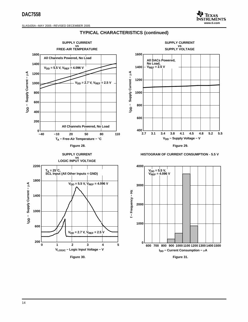
SUPPLY CURRENT SUPPLY CURRENTvs vs
FREE-AIR TEMPERATURE SUPPLY VOLTAGE
Figure 28. Figure 29.
SUPPLY CURRENT HISTOGRAM OF CURRENT CONSUMPTION - 5.5 Vvs
LOGIC INPUT VOLTAGE
Figure 30. Figure 31.
14

www.ti.com
−0.005
−0.0025
0
0.0025
0.005
0 512 1024 1536 2048 2560 3072 3584
Digital Input CodeO
utp
ut
Err
or
− V
4095
E
D
A
B, C, F, G, H
VDD = 5 V,VREF = 4.096,TA = 25C
0
500
1000
1500
2000
2500
3000
3500
4000
600 700 800 900 1000 1100 1200 1300 1400 1500
f − F
req
uen
cy −
Hz
VDD = 2.7 V,VREF = 2.5 V
IDD − Current Consumption − A
−0.005
−0.0025
0
0.0025
0.005
0 512 1024 1536 2048 2560 3072 3584Digital Input Code
Ou
tpu
t E
rro
r −
V
4095
E
D
B, C, F, G, H
VDD = 2.7 V,VREF = 2.5 V,TA = 25C
A
0
1
2
3
4
5VDD = 5 V,VREF = 4.096 V,Powerup to Code 4000
− O
utp
ut V
olta
ge
− V
VO
t − Time − 4 s/div
DAC7558
SLAS435A–MAY 2005–REVISED DECEMBER 2005
TYPICAL CHARACTERISTICS (continued)
HISTOGRAM OF CURRENT CONSUMPTION - 2.7 V TOTAL ERROR - 5 V
Figure 32. Figure 33.
TOTAL ERROR - 2.7 V EXITING POWER-DOWN MODE
Figure 34. Figure 35.
15

www.ti.com
0
1
2
3
4
5
VDD = 5 V,Output LoadedWith 200 pF to GND,Code 41 to 4055
− O
utp
ut V
olta
ge
− V
VO
t − Time − 5 s/div
0
1
2
3
VDD = 2.5 V,Output LoadedWith 200 pF to GND,Code 41 to 4055
− O
utp
ut V
olta
ge
− V
VO
t − Time − 5 s/div
Trigger Pulse
t − Time − 400 nS/div
− O
utp
ut V
olt
age
VO
VDD = 5 V, VREF = 4.096 V
Trigger Pulse
t − Time − 400 nS/div
− O
utp
ut V
olt
age
VO
VDD = 5 V, VREF = 4.096 V
DAC7558
SLAS435A–MAY 2005–REVISED DECEMBER 2005
TYPICAL CHARACTERISTICS (continued)
LARGE-SIGNAL SETTLING TIME - 5 V LARGE-SIGNAL SETTLING TIME - 2.7 V
Figure 36. Figure 37.
MIDSCALE GLITCH WORST-CASE GLITCH
Figure 38. Figure 39.
16
www.ti.com
Trigger Pulse
t − Time − 400 nS/div
− O
utp
ut V
olt
age
VO
VDD = 5 V, VREF = 4.096 V
Trigger Pulse
t − Time − 400 nS/div
− O
utp
ut V
olt
age
VO
VDD = 5 V, VREF = 4.096 V
−100
−90
−80
−70
−60
−50
−40
0 1 2 3 4 5 6 7 8 9 10
THD
2nd Harmonic
3rd Harmonic
Tota
l Har
mo
nic
Dis
tort
ion
− d
B
Output Frequency − kHz
VDD = 5 V, VREF = 4.096 V
− 1dB FSR Digital Input, Fs = 1 MspsMeasurement Bandwidth = 20 kHz
DAC7558
SLAS435A–MAY 2005–REVISED DECEMBER 2005
TYPICAL CHARACTERISTICS (continued)
DIGITAL FEEDTHROUGH ERROR CHANNEL-TO-CHANNEL CROSSTALKFOR A FULL-SCALE SWING
Figure 40. Figure 41.
TOTAL HARMONIC DISTORTIONvs
OUTPUT FREQUENCY
Figure 42.
17
www.ti.com
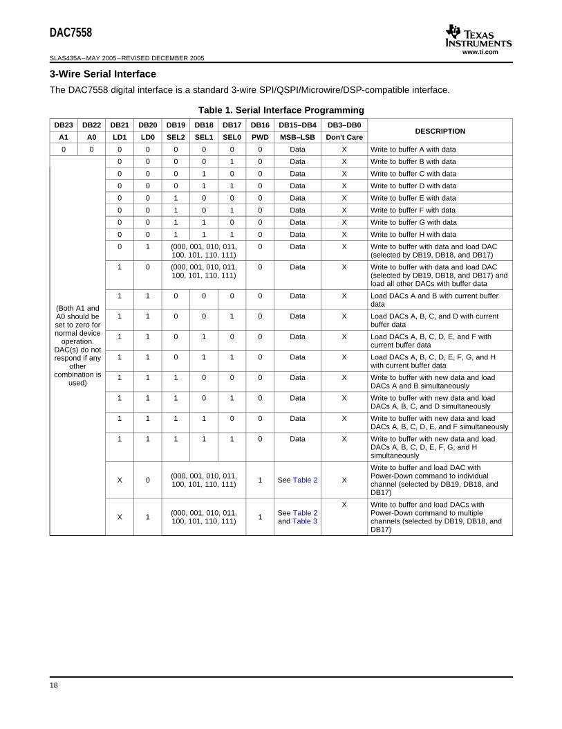
3-Wire Serial Interface
DAC7558
SLAS435A–MAY 2005–REVISED DECEMBER 2005
The DAC7558 digital interface is a standard 3-wire SPI/QSPI/Microwire/DSP-compatible interface.
Table 1. Serial Interface Programming
DB23 DB22 DB21 DB20 DB19 DB18 DB17 DB16 DB15–DB4 DB3–DB0DESCRIPTION
A1 A0 LD1 LD0 SEL2 SEL1 SEL0 PWD MSB–LSB Don't Care
0 0 0 0 0 0 0 0 Data X Write to buffer A with data
0 0 0 0 1 0 Data X Write to buffer B with data
0 0 0 1 0 0 Data X Write to buffer C with data
0 0 0 1 1 0 Data X Write to buffer D with data
0 0 1 0 0 0 Data X Write to buffer E with data
0 0 1 0 1 0 Data X Write to buffer F with data
0 0 1 1 0 0 Data X Write to buffer G with data
0 0 1 1 1 0 Data X Write to buffer H with data
0 1 (000, 001, 010, 011, 0 Data X Write to buffer with data and load DAC100, 101, 110, 111) (selected by DB19, DB18, and DB17)
1 0 (000, 001, 010, 011, 0 Data X Write to buffer with data and load DAC100, 101, 110, 111) (selected by DB19, DB18, and DB17) and
load all other DACs with buffer data
1 1 0 0 0 0 Data X Load DACs A and B with current bufferdata(Both A1 and
1 1 0 0 1 0 Data X Load DACs A, B, C, and D with currentA0 should bebuffer dataset to zero for
normal device 1 1 0 1 0 0 Data X Load DACs A, B, C, D, E, and F withoperation. current buffer data
DAC(s) do not1 1 0 1 1 0 Data X Load DACs A, B, C, D, E, F, G, and Hrespond if any
with current buffer dataothercombination is 1 1 1 0 0 0 Data X Write to buffer with new data and load
used) DACs A and B simultaneously
1 1 1 0 1 0 Data X Write to buffer with new data and loadDACs A, B, C, and D simultaneously
1 1 1 1 0 0 Data X Write to buffer with new data and loadDACs A, B, C, D, E, and F simultaneously
1 1 1 1 1 0 Data X Write to buffer with new data and loadDACs A, B, C, D, E, F, G, and Hsimultaneously
Write to buffer and load DAC with(000, 001, 010, 011, Power-Down command to individualX 0 1 See Table 2 X100, 101, 110, 111) channel (selected by DB19, DB18, and
DB17)
X Write to buffer and load DACs with(000, 001, 010, 011, See Table 2 Power-Down command to multipleX 1 1100, 101, 110, 111) and Table 3 channels (selected by DB19, DB18, and
DB17)
18
www.ti.com
THEORY OF OPERATION
D/A SECTION OUTPUT BUFFER AMPLIFIERS
DAC External Reference Input_
+Resistor StringRef +
Ref −DAC Register
VOUT
VREF
GND
VFB
100 k100 k
50 k
Amplifier Sense Input
VREFTo OutputAmplifier
RR R R GND
RESISTOR STRING
Power-On Reset
DAC7558
SLAS435A–MAY 2005–REVISED DECEMBER 2005
The architecture of the DAC7558 consists of a string The output buffer amplifier is capable of generatingDAC followed by an output buffer amplifier. Figure 43 rail-to-rail voltages on its output, which gives anshows a generalized block diagram of the DAC output range of 0 V to VDD. It is capable of driving aarchitecture. load of 2 kΩ in parallel with up to 1000 pF to GND.
The source and sink capabilities of the outputamplifier can be seen in the typical curves. The slewrate is 1 V/µs with a half-scale settling time of 3 µswith the output unloaded.
Four separate reference pins are provided for eightDACs, providing maximum flexibility. VREF1 servesDAC A and DAC B, VREF2 serves DAC C and DAC
Figure 43. Typical DAC Architecture D, VREF3 serves DAC E and DAC F, and VREF4serves DAC G and DAC H. VREF1 through VREF4can be externally shorted together for simplicity.The input coding to the DAC7558 is unsigned binary,
which gives the ideal output voltage as: It is recommended to use a buffered reference in theVOUT = VREF× D/4096 external circuit (e.g., REF3140). The input impedance
is typically 50 kΩ for each reference input pin.Where D = decimal equivalent of the binary code thatis loaded to the DAC register which can range from 0to 4095.
The DAC7558 contains eight amplifier feedback inputpins, VFBA ... VFBH. For voltage output operation,VFBA ... VFBH must externally connect to VOUTA ...VOUTH respectively. For better DC accuracy, theseconnections should be made at load points. TheVFBA ... VFBH pins are also useful for a variety ofapplications, including digitally controlled currentsources. Each feedback input pin is internallyconnected to the DAC amplifier's negative inputFigure 44. Typical Resistor Stringterminal through a 100-kΩ resistor; and, theamplifier's negative input terminal internally connectsto ground through another 100-kΩ resistor (SeeFigure 43). This forms a gain-of-two, non-inverting
The resistor string section is shown in Figure 44. It is amplifier configuration. Overall gain remains onesimply a string of resistors, each of value R. The because the resistor string has a divide-by-twoDAC7558 uses eight separate resistor strings. Each configuration. The resistance seen at each VFBx pinVREFx input pin provides the external reference is approximately 200 kΩ to ground.voltage for two resistor strings. A resistor string has100 kΩ total resistance to ground, including a 50 kΩdivide-by-two resistor. Since each VREFx pin
On power up, all internal registers are cleared and allconnects to two resistor strings, the resistance seenchannels are updated with zero-scale voltages. Untilby each VREFx pin is approximately 50 kΩ. Thevalid data is written, all DAC outputs remain in thisdivide-by-two function provided by the resistor stringstate. This is particularly useful in applications whereis compensated by a gain-of-two amplifierit is important to know the state of the DAC outputsconfiguration. The voltage is tapped off by closingwhile the device is powering up. In order not to turnone of the switches connecting the string to theon ESD protection devices, VDD should be appliedamplifier. Because it is a string of resistors, it isbefore any other pin is brought high.specified monotonic. The DAC7558 architecture uses
eight separate resistor strings to minimize During power up, all digital input pins should be set atchannel-to-channel crosstalk. logic-low voltages. Shortly after power up, if RSTSELpin is low, then all DAC outputs are at theirzero-scale voltages. If RSTSEL pin is brought high,then all DAC outputs are at their mid-scale voltages.
19
www.ti.com
Power Down
Input Data Format Selection
SERIAL INTERFACE
24-Bit Word and Input Shift Register
Asynchronous Clear
DAC7558
SLAS435A–MAY 2005–REVISED DECEMBER 2005
brought low. The RST signal resets all internalregisters, and therefore behaves like the Power-OnThe DAC7558 has a flexible power-down capabilityReset. The DAC7558 updates at the first rising edgeas described in Table 2 and Table 3. Individualof the SYNC signal that occurs after the RST pin ischannels can be powered down separately, orbrought back to high.multiple channels can be powered down
simultaneously. During a power-down condition, the If the RSTSEL pin is high, RST signal going lowuser has flexibility to select the output impedance of resets all outputs to midscale. If the RSTSEL pin iseach channel. If the PD pin is brought low, then all low, RST signal going low resets all outputs tochannels can simultaneously be powered down, with zero-scale.the output at high impedance state (High-Z).
The DAC7558 has DB16 as a power-down flag. If thisflag is set, then DB11 and DB10 select one of the DAC7558 can use unsigned binary (USB) or binarythree power-down modes of the device as described twos complement (BTC) input data formats. Formatin Table 2. selection is done by the RSTSEL pin. If the RSTSEL
is kept low, the 12-bit input data is assumed to haveTable 2. DAC7558 Power-Down Modes USB format, and any asynchronous clear operation
generates zero-scale outputs. If the RSTSEL pin isDB11 DB10 OPERATING MODEkept high, the 12-bit input data is assumed to have
0 0 PWD Hi-Z BTC format and any asynchronous clear operation0 1 PWD 1 kΩ generates mid-scale outputs.1 0 PWD 100 kΩ
1 1 PWD Hi-Z
The DAC7558 is controlled over a versatile 3-wireThe DAC7558 can also be powered down using theserial interface, which operates at clock rates up toPD pin. When the PD pins is brought low, all50 MHz and is compatible with SPI, QSPI, Microwire,channels simultaneously power down and all outputsand DSP interface standards.become high impedance. When the PD pin is brought
high, the device resumes its state before the powerdown condition.
The input shift register is 24 bits wide. DAC data isThe DAC7558 also has an option to power downloaded into the device as a 24-bit word under theindividual channels, or multiple channelscontrol of a serial clock input, SCLK, as shown in thesimultaneously selected by DB20. If DB20 = 0, thenFigure 1 timing diagram. The 24-bit word, illustratedthe user can power down the selected individualin Table 1, consists of 8 control bits, followed by 12channels. If DB20 = 1, then the user can power downdata bits and 4 don't care bits. Data format is straightthe multiple channels simultaneously as explained inbinary (RSTSEL pin = 0) or binary twos complementTable 3. Power-down mode is selected by DB11 and(RSTSEL = 1), where the most significant DAC dataDB10.bit is DB15. Data is loaded MSB first (DB23) wherethe first two bits (DB23 and DB22) should be set toTable 3. DAC7558 Power-Down Modes for Multiplezero for DAC7558 to work. The DAC7558 does notChannelsrespond to any other combination other than 00.
DB19 DB18 DB17 OPERATING MODE DB21 and DB20 (LD1 and LD0) determine if the input0 0 0 PWD Channel A-B register, DAC register, or both are updated with shift
register input data. DB19, DB18, and DB17 (SEL2,0 0 1 PWD Channel A-CSEL1, and SEL0) bits select the desired DAC(s).0 1 0 PWD Channel A-DDB16 is the power-down bit. If DB16 = 0, then it is a
0 1 1 PWD Channel A-E normal operation, if DB16 = 1, then DB11 and DB101 0 0 PWD Channel A-F determine the power-down mode (Hi-Z, 1 kΩ, or 1001 0 1 PWD Channel A-G kΩ). DB20 bit also gives the user the option of
powering down either a single channel or multiple1 1 0 PWD Channel A-Hchannels at the same time. See Power Down section1 1 1 PWD Channel A-Hfor more details.
The SYNC input is a level-triggered input that acts asa frame-synchronization signal and chip enable. Data
The DAC7558 output is asynchronously set to can only be transferred into the device while SYNC iszero-scale voltage immediately after the RST pin is low. To start the serial data transfer, SYNC should be
taken low, observing the minimum SYNC-to-SCLK
20

www.ti.com
IOVDD and Level Shifters
INTEGRAL AND DIFFERENTIAL LINEARITY
GLITCH ENERGYDaisy-Chain Operation
CHANNEL-TO-CHANNEL CROSSTALK
DAC7558
SLAS435A–MAY 2005–REVISED DECEMBER 2005
falling-edge setup time, t4. After SYNC goes low, edges are received (following a falling SYNC), theserial data is shifted into the device's input shift data stream becomes complete, and SYNC can beregister on the falling edges of SCLK for 24 clock brought high to update n devices simultaneously.pulses. Any data and clock pulses after the SDO operation is specified at a maximum SCLKtwenty-fourth falling edge of SCLK are ignored. No speed of 10 MHz.further serial data transfer occurs until SYNC is taken
Daisy-chain operation is also possible betweenhigh and low again.octal-channel DAC7558, dual-channel DAC7552, and
SYNC may be taken high after the falling edge of the single-channel DAC7551 devices. Dasy chainingtwenty-fourth SCLK pulse, observing the minimum enables communication with any number of DACSCLK Loop falling-edge to SYNC rising-edge time, t7. channels using a single serial interface. As long as
the correct number of bits are shifted using aAfter the end of serial data transfer, data is daisy-chain setting, a rising edge of SYNC properlyautomatically transferred from the input shift register updates all chips in the system. Following a risingto the input register of the selected DAC. If SYNC is edge of SYNC, all devices on the daisy chaintaken high before the twenty-fourth falling edge of respond according to the control bits they receive.SCLK, the data transfer is aborted and the DAC inputregisters are not updated.
When DCEN is low, the SDO pin is brought to a Hi-Z The DAC7558 can be used with different logicstate. The first 24 data bits that follow the falling edge families that require a wide range of supply voltagesof SYNC are stored in the shift register. The rising (from 1.8 V to 5.5 V). To enable this useful feature,edge of SYNC that follows the 24th data bit updates the IOVDD pin must be connected to the logic supplythe DAC(s). If SYNC is brought high before the 24th voltage of the system. All DAC7558 digital input anddata bit, no action occurs. output pins are equipped with level-shifter circuits.
Level shifters at the input pins ensure that externalIn daisy-chain mode (DCEN = 1) the DAC7558logic high voltages are translated to the internal logicrequires a falling SCLK edge after the rising SYNC, inhigh voltage, with no additional power dissipation.order to initialize the serial interface for the nextSimilarly, the level shifter for the SDO pin translatesupdate.the internal logic high voltage (AVDD) to the external
When DCEN is high, data can continuously be shifted logic high level (IOVDD). For single supply operation,into the shift register, enabling the daisy-chain the IOVDD pin can be tied to the AVDD pin.operation. The SDO pin becomes active and outputsSDIN data with 24 clock-cycle delay. A rising edge ofSYNC loads the shift register data into the DAC(s).The loaded data consists of the last 24 data bits The DAC7558 uses precision thin-film resistorsreceived into the shift register before the rising edge providing exceptional linearity and monotonicity.of SYNC. Integral linearity error is typically within (+/-) 0.35
LSBs, and differential linearity error is typically withinIf daisy-chain operation is not needed, DCEN should (+/-) 0.08 LSBs.permanently be tied to a logic-low voltage.
The DAC7558 uses a proprietary architecture thatWhen the DCEN pin is brought high, daisy chaining isminimizes glitch energy. The code-to-code glitchesenabled. Serial data output (SDO) pin is provided toare so low, they are usually buried within thedaisy-chain multiple DAC7558 devices in a system.wide-band noise and cannot be easily detected. TheAs long as SYNC is high or DCEN is low the SDO pinDAC7558 glitch is typically well under 0.1 nV-s. Suchis in a high-impedance state. When SYNC is broughtlow glitch energy provides more than 10Xlow the output of the internal shift register is tied toimprovement over industry alternatives.the SDO pin. As long as SYNC is low and DCEN is
high, SDO duplicates the SDIN signal with 24-cycledelay. To support multiple devices in a daisy-chain,SCLK and SYNC signals are shared across all The DAC7558 architecture is designed to minimizedevices and SDO of one DAC7558 should be tied to channel-to-channel crosstalk. The voltage change inthe SDIN of the next DAC7558. For n devices in such one channel does not affect the voltage output ina daisy chain, 24n SCLK cycles are required to shift another channel. The DC crosstalk is in the order of athe entire input data stream. After 24n SCLK falling few microvolts. AC crosstalk is also less than –100
dBs. This provides orders of magnitude improvementover certain competing architectures.
21
www.ti.com
APPLICATION INFORMATION
Waveform Generation
Generating ±5-V, ±10-V, and ± 12-V Outputs For
DAC7558
REFIN
DAC7558
_
+Vdac
R2
R1REF3140
Vref
Vtail
VOUT
OPA4130
VOUT VREFR2R1
1 Din4096
VtailR2R1 (1)
DAC7558
SLAS435A–MAY 2005–REVISED DECEMBER 2005
ringing characteristics of the loop's transfer function,DAC glitches can also slow the loop down. With its 1MSPS (small-signal) maximum data update rate,DAC7558 can support high-speed control loops.
Due to its exceptional linearity, low glitch, and low Ultra-low glitch energy of the DAC7558 significantlycrosstalk, the DAC7558 is well suited for waveform improves loop stability and loop settling time.generation (from DC to 10 kHz). The DAC7558large-signal settling time is 5 µs, supporting an Generating Industrial Voltage Ranges:update rate of 200 KSPS. However, the update rates
For control loop applications, DAC gain and offsetcan exceed 1 MSPS if the waveform to be generatederrors are not important parameters. This could beconsists of small voltage steps between consecutiveexploited to lower trim and calibration costs in aDAC updates. To obtain a high dynamic range,high-voltage control circuit design. Using a quadREF3140 (4.096 V) or REF02 (5.0 V) areoperational amplifier (OPA4130), and a voltagerecommended for reference voltage generation.reference (REF3140), the DAC7558 can generate thewide voltage swings required by the control loop.
Precision Industrial Control
Industrial control applications can require multiplefeedback loops consisting of sensors, ADCs, MCUs,DACs, and actuators. Loop accuracy and loop speedare the two important parameters of such controlloops.
Loop Accuracy:
In a control loop, the ADC has to be accurate. Offset,gain, and the integral linearity errors of the DAC arenot factors in determining the accuracy of the loop. Figure 45. Low-cost, Wide-swing VoltageAs long as a voltage exists in the transfer curve of a Generator for Control Loop Applicationsmonotonic DAC, the loop can find it and settle to it.On the other hand, DAC resolution and differential
The output voltage of the configuration is given by:linearity do determine the loop accuracy, becauseeach DAC step determines the minimum incrementalchange the loop can generate. A DNL error less than–1 LSB (non-monotonicity) can create loop instability.
Fixed R1 and R2 resistors can be used to coarselyA DNL error greater than +1 LSB impliesset the gain required in the first term of the equation.unnecessarily large voltage steps and missed voltageOnce R2 and R1 set the gain to include sometargets. With high DNL errors, the loop looses itsminimal over-range, four DAC7558 channels could bestability, resolution, and accuracy. Offering 12-bitused to precisely set the required offset voltages.ensured monotonicity and ± 0.08 LSB typical DNLResidual errors are not an issue for loop accuracyerror, 755X DACs are great choices for precisionbecause offset and gain errors could be tolerated.control loops.Four DAC7558 channels can provide the Vtail
Loop Speed: voltages to minimize offset error, while the other fourDAC7558 channels provide Vdac voltages toMany factors determine control loop speed. Typically,generate four high-voltage outputs.the ADC's conversion time, and the MCU's
computation time are the two major factors that For ±5-V operation: R1=10 kΩ, R2 = 15 kΩ, Vtail =dominate the time constant of the loop. DAC settling 3.33 V, VREF = 4.096 Vtime is rarely a dominant factor because ADC
For ±10-V operation: R1=10 kΩ, R2 = 39 kΩ, Vtail =conversion times usually exceed DAC conversion2.56 V, VREF = 4.096 Vtimes. DAC offset, gain, and linearity errors can slow
the loop down only during the start-up. Once the loop For ±12-V operation: R1=10 kΩ, R2 = 49 kΩ, Vtail =reaches its steady-state operation, these errors do 2.45 V, VREF = 4.096 Vnot affect loop speed any further. Depending on the
22

PACKAGE OPTION ADDENDUM
www.ti.com 27-Jul-2013
Addendum-Page 1
PACKAGING INFORMATION
Orderable Device Status(1)
Package Type PackageDrawing
Pins PackageQty
Eco Plan(2)
Lead/Ball Finish MSL Peak Temp(3)
Op Temp (°C) Device Marking(4/5)
Samples
DAC7558IRHBR ACTIVE VQFN RHB 32 3000 Green (RoHS& no Sb/Br)
CU NIPDAU Level-2-260C-1 YEAR -40 to 105 D758
DAC7558IRHBRG4 ACTIVE VQFN RHB 32 3000 Green (RoHS& no Sb/Br)
CU NIPDAU Level-2-260C-1 YEAR -40 to 105 D758
DAC7558IRHBT ACTIVE VQFN RHB 32 250 Green (RoHS& no Sb/Br)
CU NIPDAU Level-2-260C-1 YEAR -40 to 105 D758
DAC7558IRHBTG4 ACTIVE VQFN RHB 32 250 Green (RoHS& no Sb/Br)
CU NIPDAU Level-2-260C-1 YEAR -40 to 105 D758
(1) The marketing status values are defined as follows:ACTIVE: Product device recommended for new designs.LIFEBUY: TI has announced that the device will be discontinued, and a lifetime-buy period is in effect.NRND: Not recommended for new designs. Device is in production to support existing customers, but TI does not recommend using this part in a new design.PREVIEW: Device has been announced but is not in production. Samples may or may not be available.OBSOLETE: TI has discontinued the production of the device.
(2) Eco Plan - The planned eco-friendly classification: Pb-Free (RoHS), Pb-Free (RoHS Exempt), or Green (RoHS & no Sb/Br) - please check http://www.ti.com/productcontent for the latest availabilityinformation and additional product content details.TBD: The Pb-Free/Green conversion plan has not been defined.Pb-Free (RoHS): TI's terms "Lead-Free" or "Pb-Free" mean semiconductor products that are compatible with the current RoHS requirements for all 6 substances, including the requirement thatlead not exceed 0.1% by weight in homogeneous materials. Where designed to be soldered at high temperatures, TI Pb-Free products are suitable for use in specified lead-free processes.Pb-Free (RoHS Exempt): This component has a RoHS exemption for either 1) lead-based flip-chip solder bumps used between the die and package, or 2) lead-based die adhesive used betweenthe die and leadframe. The component is otherwise considered Pb-Free (RoHS compatible) as defined above.Green (RoHS & no Sb/Br): TI defines "Green" to mean Pb-Free (RoHS compatible), and free of Bromine (Br) and Antimony (Sb) based flame retardants (Br or Sb do not exceed 0.1% by weightin homogeneous material)
(3) MSL, Peak Temp. -- The Moisture Sensitivity Level rating according to the JEDEC industry standard classifications, and peak solder temperature.
(4) There may be additional marking, which relates to the logo, the lot trace code information, or the environmental category on the device.
(5) Multiple Device Markings will be inside parentheses. Only one Device Marking contained in parentheses and separated by a "~" will appear on a device. If a line is indented then it is a continuationof the previous line and the two combined represent the entire Device Marking for that device.
Important Information and Disclaimer:The information provided on this page represents TI's knowledge and belief as of the date that it is provided. TI bases its knowledge and belief on informationprovided by third parties, and makes no representation or warranty as to the accuracy of such information. Efforts are underway to better integrate information from third parties. TI has taken and

PACKAGE OPTION ADDENDUM
www.ti.com 27-Jul-2013
Addendum-Page 2
continues to take reasonable steps to provide representative and accurate information but may not have conducted destructive testing or chemical analysis on incoming materials and chemicals.TI and TI suppliers consider certain information to be proprietary, and thus CAS numbers and other limited information may not be available for release.
In no event shall TI's liability arising out of such information exceed the total purchase price of the TI part(s) at issue in this document sold by TI to Customer on an annual basis.

TAPE AND REEL INFORMATION
*All dimensions are nominal
Device PackageType
PackageDrawing
Pins SPQ ReelDiameter
(mm)
ReelWidth
W1 (mm)
A0(mm)
B0(mm)
K0(mm)
P1(mm)
W(mm)
Pin1Quadrant
DAC7558IRHBR VQFN RHB 32 3000 330.0 12.4 5.3 5.3 1.5 8.0 12.0 Q2
DAC7558IRHBT VQFN RHB 32 250 180.0 12.4 5.3 5.3 1.5 8.0 12.0 Q2
PACKAGE MATERIALS INFORMATION
www.ti.com 1-Nov-2016
Pack Materials-Page 1

*All dimensions are nominal
Device Package Type Package Drawing Pins SPQ Length (mm) Width (mm) Height (mm)
DAC7558IRHBR VQFN RHB 32 3000 336.6 336.6 28.6
DAC7558IRHBT VQFN RHB 32 250 210.0 185.0 35.0
PACKAGE MATERIALS INFORMATION
www.ti.com 1-Nov-2016
Pack Materials-Page 2


IMPORTANT NOTICE
Texas Instruments Incorporated and its subsidiaries (TI) reserve the right to make corrections, enhancements, improvements and otherchanges to its semiconductor products and services per JESD46, latest issue, and to discontinue any product or service per JESD48, latestissue. Buyers should obtain the latest relevant information before placing orders and should verify that such information is current andcomplete. All semiconductor products (also referred to herein as “components”) are sold subject to TI’s terms and conditions of salesupplied at the time of order acknowledgment.TI warrants performance of its components to the specifications applicable at the time of sale, in accordance with the warranty in TI’s termsand conditions of sale of semiconductor products. Testing and other quality control techniques are used to the extent TI deems necessaryto support this warranty. Except where mandated by applicable law, testing of all parameters of each component is not necessarilyperformed.TI assumes no liability for applications assistance or the design of Buyers’ products. Buyers are responsible for their products andapplications using TI components. To minimize the risks associated with Buyers’ products and applications, Buyers should provideadequate design and operating safeguards.TI does not warrant or represent that any license, either express or implied, is granted under any patent right, copyright, mask work right, orother intellectual property right relating to any combination, machine, or process in which TI components or services are used. Informationpublished by TI regarding third-party products or services does not constitute a license to use such products or services or a warranty orendorsement thereof. Use of such information may require a license from a third party under the patents or other intellectual property of thethird party, or a license from TI under the patents or other intellectual property of TI.Reproduction of significant portions of TI information in TI data books or data sheets is permissible only if reproduction is without alterationand is accompanied by all associated warranties, conditions, limitations, and notices. TI is not responsible or liable for such altereddocumentation. Information of third parties may be subject to additional restrictions.Resale of TI components or services with statements different from or beyond the parameters stated by TI for that component or servicevoids all express and any implied warranties for the associated TI component or service and is an unfair and deceptive business practice.TI is not responsible or liable for any such statements.Buyer acknowledges and agrees that it is solely responsible for compliance with all legal, regulatory and safety-related requirementsconcerning its products, and any use of TI components in its applications, notwithstanding any applications-related information or supportthat may be provided by TI. Buyer represents and agrees that it has all the necessary expertise to create and implement safeguards whichanticipate dangerous consequences of failures, monitor failures and their consequences, lessen the likelihood of failures that might causeharm and take appropriate remedial actions. Buyer will fully indemnify TI and its representatives against any damages arising out of the useof any TI components in safety-critical applications.In some cases, TI components may be promoted specifically to facilitate safety-related applications. With such components, TI’s goal is tohelp enable customers to design and create their own end-product solutions that meet applicable functional safety standards andrequirements. Nonetheless, such components are subject to these terms.No TI components are authorized for use in FDA Class III (or similar life-critical medical equipment) unless authorized officers of the partieshave executed a special agreement specifically governing such use.Only those TI components which TI has specifically designated as military grade or “enhanced plastic” are designed and intended for use inmilitary/aerospace applications or environments. Buyer acknowledges and agrees that any military or aerospace use of TI componentswhich have not been so designated is solely at the Buyer's risk, and that Buyer is solely responsible for compliance with all legal andregulatory requirements in connection with such use.TI has specifically designated certain components as meeting ISO/TS16949 requirements, mainly for automotive use. In any case of use ofnon-designated products, TI will not be responsible for any failure to meet ISO/TS16949.
Products ApplicationsAudio www.ti.com/audio Automotive and Transportation www.ti.com/automotiveAmplifiers amplifier.ti.com Communications and Telecom www.ti.com/communicationsData Converters dataconverter.ti.com Computers and Peripherals www.ti.com/computersDLP® Products www.dlp.com Consumer Electronics www.ti.com/consumer-appsDSP dsp.ti.com Energy and Lighting www.ti.com/energyClocks and Timers www.ti.com/clocks Industrial www.ti.com/industrialInterface interface.ti.com Medical www.ti.com/medicalLogic logic.ti.com Security www.ti.com/securityPower Mgmt power.ti.com Space, Avionics and Defense www.ti.com/space-avionics-defenseMicrocontrollers microcontroller.ti.com Video and Imaging www.ti.com/videoRFID www.ti-rfid.comOMAP Applications Processors www.ti.com/omap TI E2E Community e2e.ti.comWireless Connectivity www.ti.com/wirelessconnectivity
Mailing Address: Texas Instruments, Post Office Box 655303, Dallas, Texas 75265Copyright © 2016, Texas Instruments Incorporated