12-bit, high-speed, single-supply, sar adc data ... · documents tools & software support &...
TRANSCRIPT
Oscillator
CONVST/CS
PGA
1 M:
OVP
1 M:
OVP
2nd-OrderLPF
ADCDriver
VBIAS
AIN_P
AIN_GND
4.096-VReference
REFGNDDGNDAGND
DVDDAVDD
Digital Logicand Interface
REFIO
REFCAP
SCLK
SDI
SDO
12-BitSAR ADC
ADS866x
Copyright © 2016, Texas Instruments Incorporated
Product
Folder
Sample &Buy
Technical
Documents
Tools &
Software
Support &Community
ReferenceDesign
An IMPORTANT NOTICE at the end of this data sheet addresses availability, warranty, changes, use in safety-critical applications,intellectual property matters and other important disclaimers. PRODUCTION DATA.
ADS8661, ADS8665SBAS780 –DECEMBER 2016
ADS866x 12-Bit, High-Speed, Single-Supply, SAR ADC Data Acquisition Systemwith Programmable, Bipolar Input Ranges
1
1 Features1• 12-Bit ADC with Integrated Analog Front-End• High Speed:
– ADS8661: 1.25 MSPS– ADS8665: 500 kSPS
• Software Programmable Input Ranges:– Bipolar Ranges: ±12.288 V, ±10.24 V,
±6.144 V, ±5.12 V, and ±2.56 V– Unipolar Ranges: 0 V–12.288 V, 0 V–10.24 V,
0 V–6.144 V, and 0 V–5.12 V• 5-V Analog Supply: 1.65-V to 5-V I/O Supply• Constant Resistive Input Impedance ≥ 1 MΩ• Input Overvoltage Protection: Up to ±20 V• On-Chip, 4.096-V Reference with Low Drift• Excellent Performance:
– DNL: ±0.1 LSB; INL: ±0.15 LSB– SNR: 74 dB; THD: –102 dB
• ALARM → High, Low Thresholds per Channel• multiSPI™ Interface with Daisy-Chain• Extended Industrial Temperature Range:
–40°C to +125°C
2 Applications• Channel-Isolated PLC Analog Input Modules• Test and Measurement• Battery Pack Monitoring
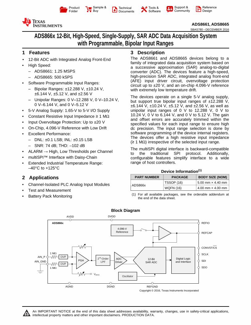
3 DescriptionThe ADS8661 and ADS8665 devices belong to afamily of integrated data acquisition system based ona successive approximation (SAR) analog-to-digitalconverter (ADC). The devices feature a high-speed,high-precision SAR ADC, integrated analog front-end(AFE) input driver circuit, overvoltage protectioncircuit up to ±20 V, and an on-chip 4.096-V referencewith extremely low temperature drift.
The devices operate on a single 5-V analog supply,but support true bipolar input ranges of ±12.288 V,±6.144 V, ±10.24 V, ±5.12 V, and ±2.56 V, as well asunipolar input ranges of 0 V to 12.288 V, 0 V to10.24 V, 0 V to 6.144 V, and 0 V to 5.12 V. The gainand offset errors are accurately trimmed within thespecified values for each input range to ensure highdc precision. The input range selection is done bysoftware programming of the device internal registers.The devices offer a high resistive input impedance(≥ 1 MΩ) irrespective of the selected input range.
The multiSPI digital interface is backward-compatibleto the traditional SPI protocol. Additionally,configurable features simplify interface to a widerange of host controllers.
Device Information(1)
PART NUMBER PACKAGE BODY SIZE (NOM)
ADS866xTSSOP (16) 5.00 mm × 4.40 mmWQFN (16) 4.00 mm × 4.00 mm
(1) For all available packages, see the orderable addendum atthe end of the data sheet.
Block Diagram

2
ADS8661, ADS8665SBAS780 –DECEMBER 2016 www.ti.com
Product Folder Links: ADS8661 ADS8665
Submit Documentation Feedback Copyright © 2016, Texas Instruments Incorporated
Table of Contents1 Features .................................................................. 12 Applications ........................................................... 13 Description ............................................................. 14 Revision History..................................................... 25 Pin Configuration and Functions ......................... 36 Specifications......................................................... 4
6.1 Absolute Maximum Ratings ...................................... 46.2 ESD Ratings.............................................................. 46.3 Recommended Operating Conditions....................... 46.4 Thermal Information .................................................. 46.5 Electrical Characteristics........................................... 56.6 Timing Requirements: Conversion Cycle.................. 86.7 Timing Requirements: Asynchronous Reset............. 86.8 Timing Requirements: SPI-Compatible Serial
Interface ..................................................................... 86.9 Timing Requirements: Source-Synchronous Serial
Interface (External Clock) .......................................... 96.10 Timing Requirements: Source-Synchronous Serial
Interface (Internal Clock)............................................ 96.11 Typical Characteristics .......................................... 13
7 Detailed Description ............................................ 207.1 Overview ................................................................. 207.2 Functional Block Diagram ....................................... 20
7.3 Feature Description................................................. 217.4 Device Functional Modes........................................ 337.5 Programming........................................................... 387.6 Register Maps ......................................................... 46
8 Application and Implementation ........................ 548.1 Application Information............................................ 548.2 Typical Application ................................................. 54
9 Power Supply Recommendations ...................... 579.1 Power Supply Decoupling....................................... 579.2 Power Saving .......................................................... 57
10 Layout................................................................... 5810.1 Layout Guidelines ................................................. 5810.2 Layout Example .................................................... 59
11 Device and Documentation Support ................. 6011.1 Documentation Support ........................................ 6011.2 Related Links ........................................................ 6011.3 Receiving Notification of Documentation Updates 6011.4 Community Resources.......................................... 6011.5 Trademarks ........................................................... 6011.6 Electrostatic Discharge Caution............................ 6011.7 Glossary ................................................................ 60
12 Mechanical, Packaging, and OrderableInformation ........................................................... 61
4 Revision History
DATE REVISION NOTESDecember 2016 * Initial release.

RV
S
ALARM/SDO-1/GPO
SDO-0
CONVST/CS
SCLK
SD
I
RS
T
AIN
_GN
D
AIN
_P
AGND
REFIO
REFGND
REFCAP
AV
DD
DG
ND
DV
DD
1
2
3
4
16
15
14
13
ALARM/SDO-1/GPO
SDO-0
CONVST/CS
SDI
RST
DGND
AVDD
SCLK
AGND
REFIO
REFGND
REFCAP
5
6
7
8
12
11
10
9
AIN_P
AIN_GND
DVDD
RVS
3
ADS8661, ADS8665www.ti.com SBAS780 –DECEMBER 2016
Product Folder Links: ADS8661 ADS8665
Submit Documentation FeedbackCopyright © 2016, Texas Instruments Incorporated
5 Pin Configuration and Functions
PW Package16-Pin TSSOP
Top View (Not to Scale)
RUM Package16-Pin WQFN
Top View (Not to Scale)
(1) AI = analog input, AIO = analog input/output, DI = digital input, DO = digital output, and P = power supply.
Pin Functions
NAMENO.
TYPE (1) DESCRIPTIONTSSOP WQFN
AGND 3 1 P Analog ground pin. Decouple with the AVDD pin.
AIN_GND 8 6 AI Analog input: negative. Decouple with the AIN_P pin.
AIN_P 7 5 AI Analog input: positive. Decouple with the AIN_GND pin.
ALARM/SDO-1/GPO 14 12 DO Multi-function output pin. Active high alarm.Data output 1 for serial communication. General-purpose output pin.
AVDD 2 16 P Analog supply pin. Decouple with the AGND pin.
CONVST/CS 11 9 DI
Dual-functionality pin.Active high logic: conversion start input pin; a CONVST rising edge brings the device fromacquisition phase to conversion phase.Active low logic: chip-select input pin; the device takes control of the data bus when CS is low;the SDO-x pins go to tri-state when CS is high.
DGND 1 15 P Digital ground pin. Decouple with the DVDD pin.
DVDD 16 14 P Digital supply pin. Decouple with the DGND pin.
REFCAP 6 4 AO ADC reference buffer decoupling capacitor pin. Decouple with the REFGND pin.
REFGND 5 3 P Reference ground pin; short to the analog ground plane. Decouple with the REFIO andREFCAP pins.
REFIO 4 2 AIO Internal reference output and external reference input pin. Decouple with REFGND.
RST 9 7 DI Active low logic input to reset the device.
RVS 15 13 DOMulti-function output pin for serial interface; see the RESET State section.With CS held high, RVS reflects the status of the internal ADCST signal.With CS low, the status of RVS depends on the output protocol selection.
SCLK 12 10 DI Serial communication: clock input pin for the serial interface.All system-synchronous data transfer protocols are timed with respect to the SCLK signal.
SDI 10 8 DI Dual function: data input pin for serial communication.Chain data input during serial communication in daisy-chain mode.
SDO-0 13 11 DO Serial communication: data output 0
4
ADS8661, ADS8665SBAS780 –DECEMBER 2016 www.ti.com
Product Folder Links: ADS8661 ADS8665
Submit Documentation Feedback Copyright © 2016, Texas Instruments Incorporated
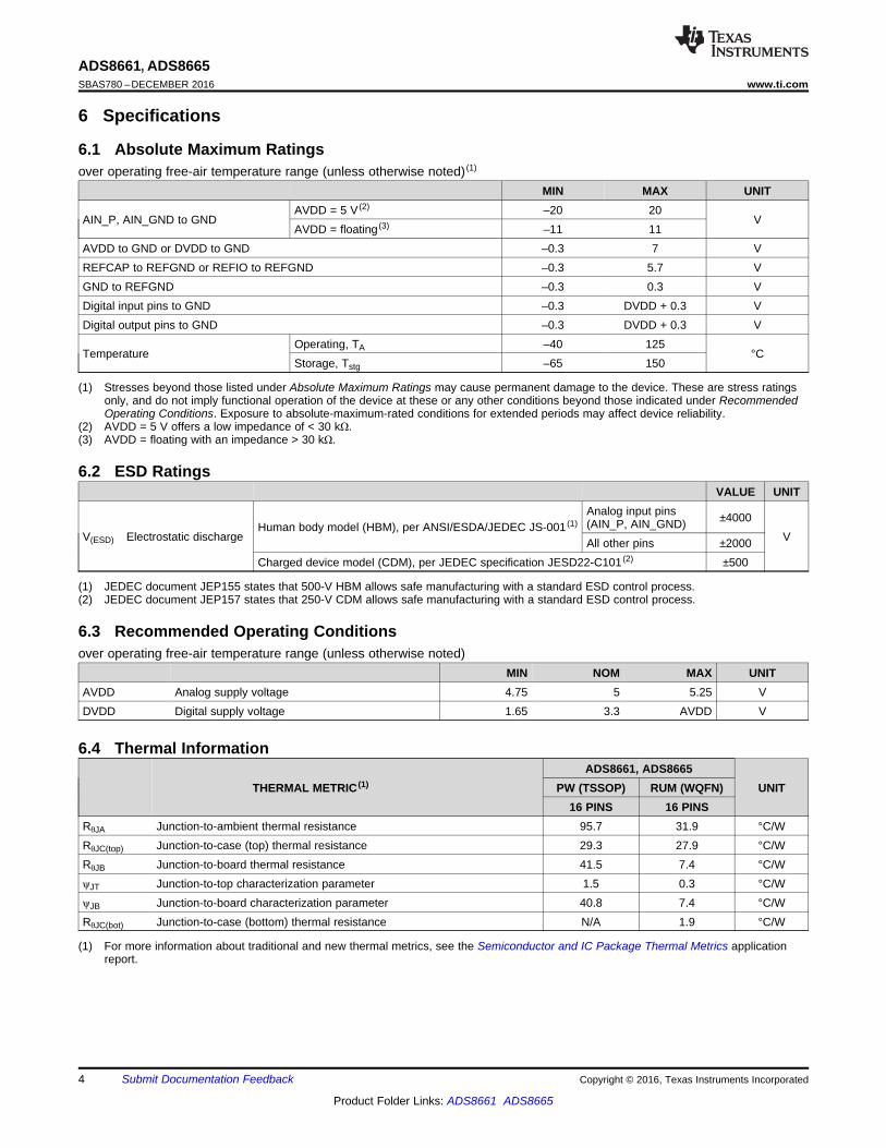
(1) Stresses beyond those listed under Absolute Maximum Ratings may cause permanent damage to the device. These are stress ratingsonly, and do not imply functional operation of the device at these or any other conditions beyond those indicated under RecommendedOperating Conditions. Exposure to absolute-maximum-rated conditions for extended periods may affect device reliability.
(2) AVDD = 5 V offers a low impedance of < 30 kΩ.(3) AVDD = floating with an impedance > 30 kΩ.
6 Specifications
6.1 Absolute Maximum Ratingsover operating free-air temperature range (unless otherwise noted) (1)
MIN MAX UNIT
AIN_P, AIN_GND to GNDAVDD = 5 V (2) –20 20
VAVDD = floating (3) –11 11
AVDD to GND or DVDD to GND –0.3 7 VREFCAP to REFGND or REFIO to REFGND –0.3 5.7 VGND to REFGND –0.3 0.3 VDigital input pins to GND –0.3 DVDD + 0.3 VDigital output pins to GND –0.3 DVDD + 0.3 V
TemperatureOperating, TA –40 125
°CStorage, Tstg –65 150
(1) JEDEC document JEP155 states that 500-V HBM allows safe manufacturing with a standard ESD control process.(2) JEDEC document JEP157 states that 250-V CDM allows safe manufacturing with a standard ESD control process.
6.2 ESD RatingsVALUE UNIT
V(ESD) Electrostatic dischargeHuman body model (HBM), per ANSI/ESDA/JEDEC JS-001 (1)
Analog input pins(AIN_P, AIN_GND) ±4000
VAll other pins ±2000Charged device model (CDM), per JEDEC specification JESD22-C101 (2) ±500
6.3 Recommended Operating Conditionsover operating free-air temperature range (unless otherwise noted)
MIN NOM MAX UNITAVDD Analog supply voltage 4.75 5 5.25 VDVDD Digital supply voltage 1.65 3.3 AVDD V
(1) For more information about traditional and new thermal metrics, see the Semiconductor and IC Package Thermal Metrics applicationreport.
6.4 Thermal Information
THERMAL METRIC (1)ADS8661, ADS8665
UNITPW (TSSOP) RUM (WQFN)16 PINS 16 PINS
RθJA Junction-to-ambient thermal resistance 95.7 31.9 °C/WRθJC(top) Junction-to-case (top) thermal resistance 29.3 27.9 °C/WRθJB Junction-to-board thermal resistance 41.5 7.4 °C/WψJT Junction-to-top characterization parameter 1.5 0.3 °C/WψJB Junction-to-board characterization parameter 40.8 7.4 °C/WRθJC(bot) Junction-to-case (bottom) thermal resistance N/A 1.9 °C/W

5
ADS8661, ADS8665www.ti.com SBAS780 –DECEMBER 2016
Product Folder Links: ADS8661 ADS8665
Submit Documentation FeedbackCopyright © 2016, Texas Instruments Incorporated
(1) Ideal input span, does not include gain or offset error.
6.5 Electrical Characteristicsall minimum and maximum specifications are at TA = –40°C to +125°C; typical specifications are at TA = 25°C; AVDD = 5 V,DVDD = 3.3 V, VREF = 4.096 V (internal), and maximum throughput (unless otherwise noted)
PARAMETER TEST CONDITIONS MIN TYP MAX UNIT
ANALOG INPUTS
VINFull-scale input span (1)
(AIN_P to AIN_GND)
Input range = ±3 × VREF –12.288 12.288
V
Input range = ±2.5 × VREF –10.24 10.24
Input range = ±1.5 × VREF –6.144 6.144
Input range = ±1.25 × VREF –5.12 5.12
Input range = ±0.625 × VREF –2.56 2.56
Input range = 3 × VREF 0 12.288
Input range = 2.5 × VREF 0 10.24
Input range = 1.5 × VREF 0 6.144
Input range = 1.25 × VREF 0 5.12
AIN_P Operating input range
Input range = ±3 × VREF –12.288 12.288
V
Input range = ±2.5 × VREF –10.24 10.24
Input range = ±1.5 × VREF –6.144 6.144
Input range = ±1.25 × VREF –5.12 5.12
Input range = ±0.625 × VREF –2.56 2.56
Input range = 3 × VREF 0 12.288
Input range = 2.5 × VREF 0 10.24
Input range = 1.5 × VREF 0 6.144
Input range = 1.25 × VREF 0 5.12
AIN_GND Operating input range All input ranges –0.1 0 0.1 V
RIN Input impedance At TA = 25°C
Input range = ±3 × VREF 1.02 1.2 1.38
MΩ
Input range = ±1.5 × VREF 1.02 1.2 1.38
Input range = 3 × VREF 1.02 1.2 1.38
Input range = 1.5 × VREF 1.02 1.2 1.38
Input range = ±2.5 × VREF 0.85 1 1.15
Input range = ±1.25 × VREF 0.85 1 1.15
Input range = ±0.625 × VREF 0.85 1 1.15
Input range = 2.5 × VREF 0.85 1 1.15
Input range = 1.25 × VREF 0.85 1 1.15
Input impedance drift 7 25 ppm/°C
IIN Input currentWith voltageat the AIN_Ppin = VIN
Input range = ±3 × VREF (VIN – 2.5) / RIN
µA
Input range = ±2.5 × VREF (VIN – 2.2) / RIN
Input range = ±1.5 × VREF (VIN – 2.0) / RIN
Input range = ±1.25 × VREF (VIN – 2.0) / RIN
Input range = ±0.625 × VREF (VIN – 1.6) / RIN
Input range = 3 × VREF (VIN – 2.6) / RIN
Input range = 2.5 × VREF (VIN – 2.5) / RIN
Input range = 1.5 × VREF (VIN – 2.7) / RIN
Input range = 1.25 × VREF (VIN – 2.5) / RIN
INPUT OVERVOLTAGE PROTECTION CIRCUIT
VOVP All input ranges
AVDD = 5 V or offers low impedance < 30 kΩ,all input ranges –20 20
VAVDD = floating with impedance > 30 kΩ,all input ranges –11 11
INPUT BANDWIDTH
f–3 dB Small-signal Inputbandwidth
–3 dB All input ranges 15kHz
f–0.1 dB –0.1 dB All input ranges 2.5
6
ADS8661, ADS8665SBAS780 –DECEMBER 2016 www.ti.com
Product Folder Links: ADS8661 ADS8665
Submit Documentation Feedback Copyright © 2016, Texas Instruments Incorporated
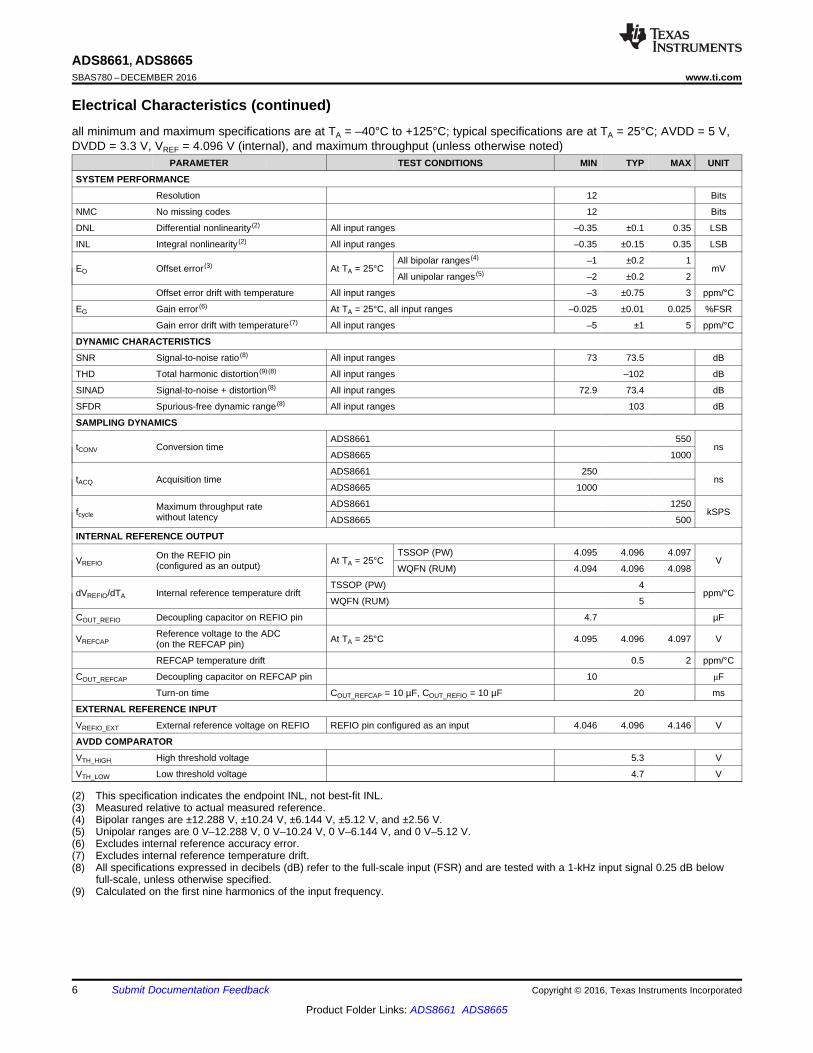
Electrical Characteristics (continued)all minimum and maximum specifications are at TA = –40°C to +125°C; typical specifications are at TA = 25°C; AVDD = 5 V,DVDD = 3.3 V, VREF = 4.096 V (internal), and maximum throughput (unless otherwise noted)
PARAMETER TEST CONDITIONS MIN TYP MAX UNIT
(2) This specification indicates the endpoint INL, not best-fit INL.(3) Measured relative to actual measured reference.(4) Bipolar ranges are ±12.288 V, ±10.24 V, ±6.144 V, ±5.12 V, and ±2.56 V.(5) Unipolar ranges are 0 V–12.288 V, 0 V–10.24 V, 0 V–6.144 V, and 0 V–5.12 V.(6) Excludes internal reference accuracy error.(7) Excludes internal reference temperature drift.(8) All specifications expressed in decibels (dB) refer to the full-scale input (FSR) and are tested with a 1-kHz input signal 0.25 dB below
full-scale, unless otherwise specified.(9) Calculated on the first nine harmonics of the input frequency.
SYSTEM PERFORMANCE
Resolution 12 Bits
NMC No missing codes 12 Bits
DNL Differential nonlinearity (2) All input ranges –0.35 ±0.1 0.35 LSB
INL Integral nonlinearity (2) All input ranges –0.35 ±0.15 0.35 LSB
EO Offset error (3) At TA = 25°CAll bipolar ranges (4) –1 ±0.2 1
mVAll unipolar ranges (5) –2 ±0.2 2
Offset error drift with temperature All input ranges –3 ±0.75 3 ppm/°C
EG Gain error (6) At TA = 25°C, all input ranges –0.025 ±0.01 0.025 %FSR
Gain error drift with temperature (7) All input ranges –5 ±1 5 ppm/°C
DYNAMIC CHARACTERISTICS
SNR Signal-to-noise ratio (8) All input ranges 73 73.5 dB
THD Total harmonic distortion (9) (8) All input ranges –102 dB
SINAD Signal-to-noise + distortion (8) All input ranges 72.9 73.4 dB
SFDR Spurious-free dynamic range (8) All input ranges 103 dB
SAMPLING DYNAMICS
tCONV Conversion timeADS8661 550
nsADS8665 1000
tACQ Acquisition timeADS8661 250
nsADS8665 1000
fcycleMaximum throughput ratewithout latency
ADS8661 1250kSPS
ADS8665 500
INTERNAL REFERENCE OUTPUT
VREFIOOn the REFIO pin(configured as an output) At TA = 25°C
TSSOP (PW) 4.095 4.096 4.097V
WQFN (RUM) 4.094 4.096 4.098
dVREFIO/dTA Internal reference temperature driftTSSOP (PW) 4
ppm/°CWQFN (RUM) 5
COUT_REFIO Decoupling capacitor on REFIO pin 4.7 µF
VREFCAPReference voltage to the ADC(on the REFCAP pin) At TA = 25°C 4.095 4.096 4.097 V
REFCAP temperature drift 0.5 2 ppm/°C
COUT_REFCAP Decoupling capacitor on REFCAP pin 10 μF
Turn-on time COUT_REFCAP = 10 µF, COUT_REFIO = 10 µF 20 ms
EXTERNAL REFERENCE INPUT
VREFIO_EXT External reference voltage on REFIO REFIO pin configured as an input 4.046 4.096 4.146 V
AVDD COMPARATOR
VTH_HIGH High threshold voltage 5.3 V
VTH_LOW Low threshold voltage 4.7 V

7
ADS8661, ADS8665www.ti.com SBAS780 –DECEMBER 2016
Product Folder Links: ADS8661 ADS8665
Submit Documentation FeedbackCopyright © 2016, Texas Instruments Incorporated
Electrical Characteristics (continued)all minimum and maximum specifications are at TA = –40°C to +125°C; typical specifications are at TA = 25°C; AVDD = 5 V,DVDD = 3.3 V, VREF = 4.096 V (internal), and maximum throughput (unless otherwise noted)
PARAMETER TEST CONDITIONS MIN TYP MAX UNIT
POWER-SUPPLY REQUIREMENTS
AVDD Analog power-supply voltage 4.75 5 5.25
VDVDD Digital power-supply voltage
Operating range 1.65 3.3 AVDD
Supply range for specified performance 2.7 3.3 AVDD
IAVDD_DYN
Analog supply current,device converting at maximumthroughput
Internalreference
ADS8661 7 9
mAADS8665 4.9 6.5
Externalreference
ADS8661 5.8 7.25
ADS8665 3.7 4.5
IAVDD_STCAnalog supply current,device not converting
Internal reference 2.9 4mA
External reference 1.7 2.25
IAVDD_STDBYAnalog supply current,device in STANDBY mode
Internal reference 2.8mA
External reference 1.6
IAVDD_PDAnalog supply current,device in PD mode
Internal reference 10μA
External reference 10
IDVDD_DYNDigital supply current,maximum throughput 0.2 0.25 mA
IDVDD_STDBYDigital supply current,device in STANDBY mode 1 μA
IDVDD_PDDigital supply current,device in PD mode 1 μA
DIGITAL INPUTS (CMOS)
VIH Digital high input voltage logic levelDVDD > 2.35 V 0.7 ×
DVDDDVDD +
0.3V
DVDD ≤ 2.35 V 0.8 ×DVDD
DVDD +0.3
VIL Digital low input voltage logic levelDVDD > 2.35 V –0.3 0.3 ×
DVDDV
DVDD ≤ 2.35 V –0.3 0.2 ×DVDD
Input leakage current 100 nA
Input pin capacitance 5 pF
DIGITAL OUTPUTS (CMOS)
VOH Digital high output voltage logic level IO = 500-μA source 0.8 ×DVDD DVDD V
VOL Digital low output voltage logic level IO = 500-μA sink 0 0.2 ×DVDD V
Floating state leakage current Only for digital output pins 1 µA
Internal pin capacitance 5 pF
TEMPERATURE RANGE
TA Operating free-air temperature –40 125 °C
8
ADS8661, ADS8665SBAS780 –DECEMBER 2016 www.ti.com
Product Folder Links: ADS8661 ADS8665
Submit Documentation Feedback Copyright © 2016, Texas Instruments Incorporated
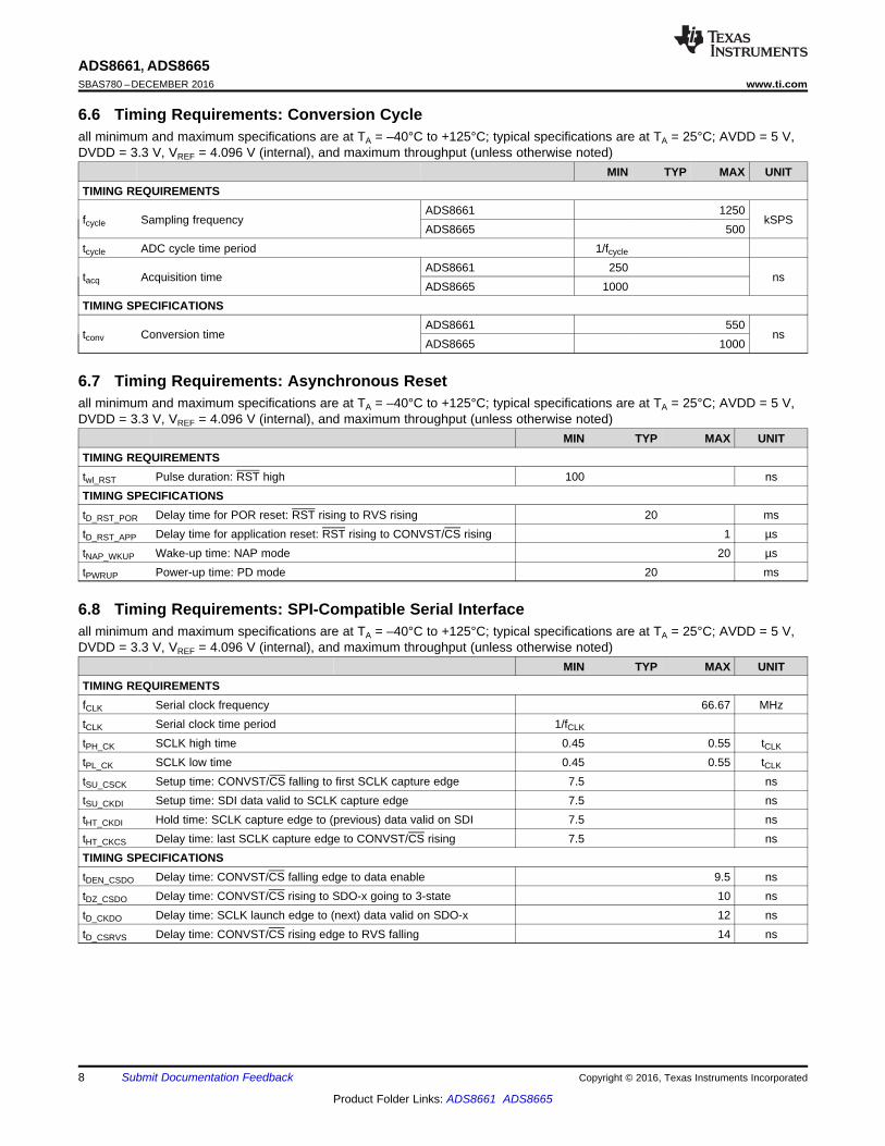
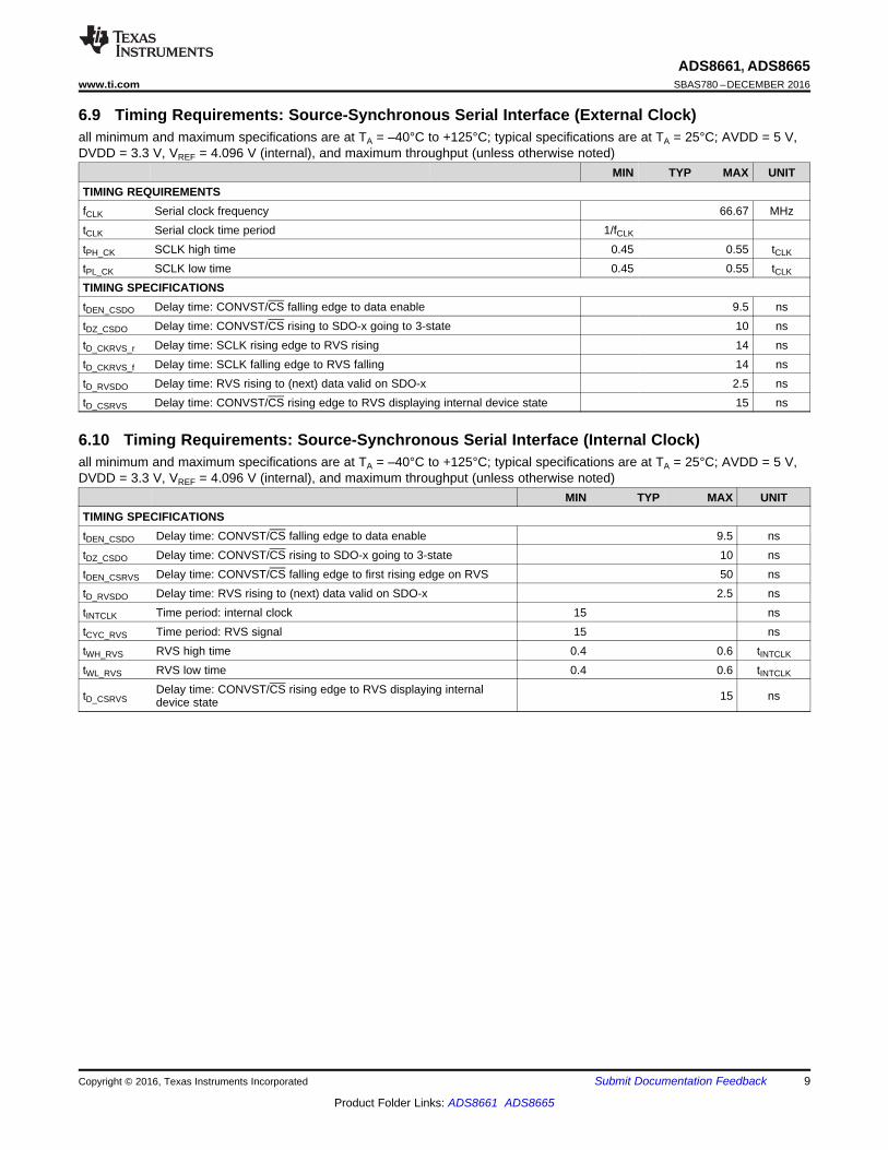
6.6 Timing Requirements: Conversion Cycleall minimum and maximum specifications are at TA = –40°C to +125°C; typical specifications are at TA = 25°C; AVDD = 5 V,DVDD = 3.3 V, VREF = 4.096 V (internal), and maximum throughput (unless otherwise noted)
MIN TYP MAX UNITTIMING REQUIREMENTS
fcycle Sampling frequencyADS8661 1250
kSPSADS8665 500
tcycle ADC cycle time period 1/fcycle
tacq Acquisition timeADS8661 250
nsADS8665 1000
TIMING SPECIFICATIONS
tconv Conversion timeADS8661 550
nsADS8665 1000
6.7 Timing Requirements: Asynchronous Resetall minimum and maximum specifications are at TA = –40°C to +125°C; typical specifications are at TA = 25°C; AVDD = 5 V,DVDD = 3.3 V, VREF = 4.096 V (internal), and maximum throughput (unless otherwise noted)
MIN TYP MAX UNITTIMING REQUIREMENTStwl_RST Pulse duration: RST high 100 nsTIMING SPECIFICATIONStD_RST_POR Delay time for POR reset: RST rising to RVS rising 20 mstD_RST_APP Delay time for application reset: RST rising to CONVST/CS rising 1 µstNAP_WKUP Wake-up time: NAP mode 20 µstPWRUP Power-up time: PD mode 20 ms
6.8 Timing Requirements: SPI-Compatible Serial Interfaceall minimum and maximum specifications are at TA = –40°C to +125°C; typical specifications are at TA = 25°C; AVDD = 5 V,DVDD = 3.3 V, VREF = 4.096 V (internal), and maximum throughput (unless otherwise noted)
MIN TYP MAX UNITTIMING REQUIREMENTSfCLK Serial clock frequency 66.67 MHztCLK Serial clock time period 1/fCLK
tPH_CK SCLK high time 0.45 0.55 tCLK
tPL_CK SCLK low time 0.45 0.55 tCLK
tSU_CSCK Setup time: CONVST/CS falling to first SCLK capture edge 7.5 nstSU_CKDI Setup time: SDI data valid to SCLK capture edge 7.5 nstHT_CKDI Hold time: SCLK capture edge to (previous) data valid on SDI 7.5 nstHT_CKCS Delay time: last SCLK capture edge to CONVST/CS rising 7.5 nsTIMING SPECIFICATIONStDEN_CSDO Delay time: CONVST/CS falling edge to data enable 9.5 nstDZ_CSDO Delay time: CONVST/CS rising to SDO-x going to 3-state 10 nstD_CKDO Delay time: SCLK launch edge to (next) data valid on SDO-x 12 nstD_CSRVS Delay time: CONVST/CS rising edge to RVS falling 14 ns
9
ADS8661, ADS8665www.ti.com SBAS780 –DECEMBER 2016
Product Folder Links: ADS8661 ADS8665
Submit Documentation FeedbackCopyright © 2016, Texas Instruments Incorporated
6.9 Timing Requirements: Source-Synchronous Serial Interface (External Clock)all minimum and maximum specifications are at TA = –40°C to +125°C; typical specifications are at TA = 25°C; AVDD = 5 V,DVDD = 3.3 V, VREF = 4.096 V (internal), and maximum throughput (unless otherwise noted)
MIN TYP MAX UNITTIMING REQUIREMENTSfCLK Serial clock frequency 66.67 MHztCLK Serial clock time period 1/fCLK
tPH_CK SCLK high time 0.45 0.55 tCLK
tPL_CK SCLK low time 0.45 0.55 tCLK
TIMING SPECIFICATIONStDEN_CSDO Delay time: CONVST/CS falling edge to data enable 9.5 nstDZ_CSDO Delay time: CONVST/CS rising to SDO-x going to 3-state 10 nstD_CKRVS_r Delay time: SCLK rising edge to RVS rising 14 nstD_CKRVS_f Delay time: SCLK falling edge to RVS falling 14 nstD_RVSDO Delay time: RVS rising to (next) data valid on SDO-x 2.5 nstD_CSRVS Delay time: CONVST/CS rising edge to RVS displaying internal device state 15 ns
6.10 Timing Requirements: Source-Synchronous Serial Interface (Internal Clock)all minimum and maximum specifications are at TA = –40°C to +125°C; typical specifications are at TA = 25°C; AVDD = 5 V,DVDD = 3.3 V, VREF = 4.096 V (internal), and maximum throughput (unless otherwise noted)
MIN TYP MAX UNITTIMING SPECIFICATIONStDEN_CSDO Delay time: CONVST/CS falling edge to data enable 9.5 nstDZ_CSDO Delay time: CONVST/CS rising to SDO-x going to 3-state 10 nstDEN_CSRVS Delay time: CONVST/CS falling edge to first rising edge on RVS 50 nstD_RVSDO Delay time: RVS rising to (next) data valid on SDO-x 2.5 nstINTCLK Time period: internal clock 15 nstCYC_RVS Time period: RVS signal 15 nstWH_RVS RVS high time 0.4 0.6 tINTCLK
tWL_RVS RVS low time 0.4 0.6 tINTCLK
tD_CSRVSDelay time: CONVST/CS rising edge to RVS displaying internaldevice state 15 ns
SCLK
Data Read Time
tSU_CSCK
SDO-0
tDEN_CSDO tD_CKDO
M M-1 M-2 L+1 L
tD_CSDO
tHT_CKCS
SDI
tSU_CKDI
tHT_CKDI
tconv_max
tD_CSRVS
RVS
tcycle
tD_CSRVS
CPOL = 0
CPOL = 1
CONVST/CS
RVS
twl_RST
RST
trst
td_rst
ADCST (Internal)
tcycle
RVS
tconv tacq
CONVST/CS
The CS falling edge can be issued after tconv_max or when RVS goes high.
10
ADS8661, ADS8665SBAS780 –DECEMBER 2016 www.ti.com
Product Folder Links: ADS8661 ADS8665
Submit Documentation Feedback Copyright © 2016, Texas Instruments Incorporated
Figure 1. Conversion Cycle Timing Diagram
Figure 2. Asynchronous Reset Timing Diagram
Figure 3. Standard SPI Interface Timing Diagram for CPHA = 0
SCLK
Data Read Time
tSU_CSCK
SDO-0
tDEN_CSDO tD_CKDO
M M-2 M-4 L+3 L+1
tD_CSDO
tHT_CKCS
SDI
tSU_CKDI
tHT_CKDI
tconv_max
tD_CSRVS
RVS
tcycle
tD_CSRVS
CPOL = 0
CPOL = 1
CONVST/CS
SDO-1 M-1 M-3 M-5 L+2 L
SCLK
Data Read Time
tSU_CSCK
SDO-0tDEN_CSDO tD_CKDO
0 M M-1 L+1 L
tDZ_CSDO
tHT_CKCS
SDI
tSU_CKDI
tHT_CKDI
tconv_max
tcycle
tD_CSRVS
RVS
tD_CSRVS
CPOL = 0
CPOL = 1
CONVST/CS
11
ADS8661, ADS8665www.ti.com SBAS780 –DECEMBER 2016
Product Folder Links: ADS8661 ADS8665
Submit Documentation FeedbackCopyright © 2016, Texas Instruments Incorporated
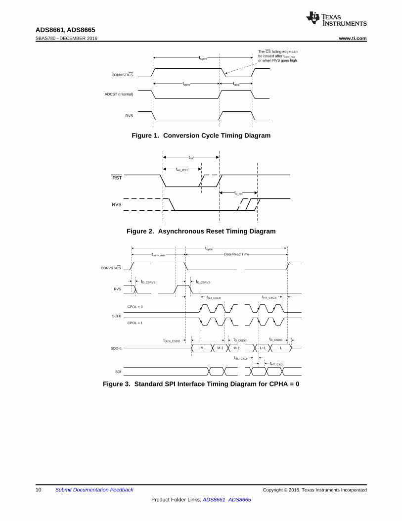
Figure 4. Standard SPI Interface Timing Diagram for CPHA = 1
Figure 5. multiSPI Interface Timing Diagram for Dual SDO-x and CPHA = 0
SCLK
Data Read Time
SDO-0 M L+1 LM-k M-k-1 M-k-2
tconv_max
RVS
tD_CSRVS
M-1
tCYC_RVS
tD_RVSDO
CONVST/CS
tDZ_CSDOtDEN_CSDO
tDEN_CSRVS tWH_RVS
tWL_RVS
SCLK
Data Read Time
SDO-0 M L+1 LM-k M-k-1 M-k-2
tconv
RVS
tSU_CSCK
tD_RVSDO
tD_CSRVS
M-1
tD_CKRVS_f
tD_CKRVS_r
tD_CSRD
CONVST/CS
tDZ_CSDOtDEN_CSDO
SCLK
Data Read Time
tSU_CSCK
SDO-0
tDEN_CSDO tD_CKDO
0 M M-2 L+3 L+1
tDZ_CSDO
tHT_CKCS
SDI
tSU_CKDI
tHT_CKDI
tconv_max
tcycle
tD_CSRVS
RVS
tD_CSRVS
CPOL = 0
CPOL = 1
CONVST/CS
0 M-1 M-1 L+2 LSDO-1
12
ADS8661, ADS8665SBAS780 –DECEMBER 2016 www.ti.com
Product Folder Links: ADS8661 ADS8665
Submit Documentation Feedback Copyright © 2016, Texas Instruments Incorporated
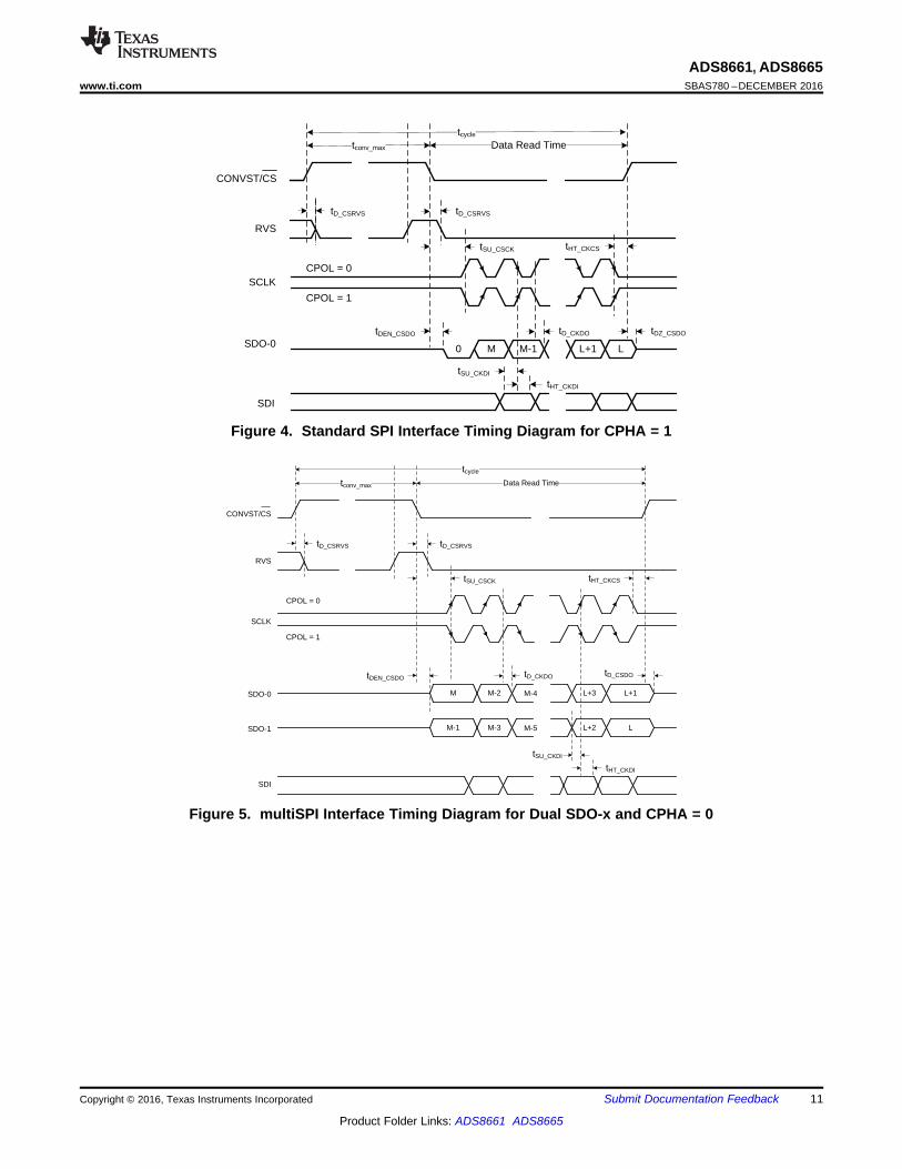
Figure 6. multiSPI Interface Timing Diagram for Dual SDO-x and CPHA = 1
Figure 7. multiSPI Source-Synchronous External Clock Serial Interface Timing Diagram
Figure 8. multiSPI Source-Synchronous Internal Clock Serial Interface Timing Diagram
Output Codes
Num
ber
of H
its
0
15000
30000
45000
60000
75000
2045 2046 2047
D001Output Codes
Num
ber
of H
its
0
15000
30000
45000
60000
75000
2045 2046 2047
D002
Free- Air Temperature (qC)
Inpu
t Im
peda
nce
Drif
t (pp
m)
-40 -7 26 59 92 125-400
-200
0
200
400
D003
±12.288 V±10.24 V±6.144 V±5.12 V±2.56 V
0-12.288 V0-10.24 V0-6.144 V0-5.12 V
Input Impedance (M:)
Num
ber
of D
evic
es
0
200
400
600
800
1000
1200
1400
1600
1.02 1.06 1.1 1.14 1.18 1.22 1.26 1.3 1.34 1.38
D004
Input Voltage (V)
Ana
log
Inpu
t Cur
rent
(uA
)
-12.288 -8.192 -4.096 0 4.096 8.192 12.288-15
-9
-3
3
9
15
D001
± 12.288 V± 10.24 V± 6.144 V± 5.12 V± 2.56 V0-12.288 V0-10.24 V0-6.144 V0-5.12 V
Input Voltage (V)
Ana
log
Inpu
t Cur
rent
(uA
)
-12.288 -8.192 -4.096 0 4.096 8.192 12.288-15
-9
-3
3
9
15
D002
-40C25C125C
13
ADS8661, ADS8665www.ti.com SBAS780 –DECEMBER 2016
Product Folder Links: ADS8661 ADS8665
Submit Documentation FeedbackCopyright © 2016, Texas Instruments Incorporated
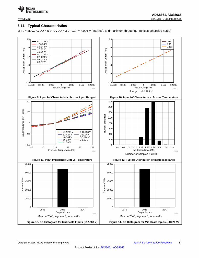
6.11 Typical Characteristicsat TA = 25°C, AVDD = 5 V, DVDD = 3 V, VREF = 4.096 V (internal), and maximum throughput (unless otherwise noted)
Figure 9. Input I-V Characteristic Across Input Ranges
Range = ±12.288 V
Figure 10. Input I-V Characteristic Across Temperature
Figure 11. Input Impedance Drift vs Temperature
Number of samples = 3398
Figure 12. Typical Distribution of Input Impedance
Mean = 2046, sigma = 0, input = 0 V
Figure 13. DC Histogram for Mid-Scale Inputs (±12.288 V)
Mean = 2046, sigma = 0, input = 0 V
Figure 14. DC Histogram for Mid-Scale Inputs (±10.24 V)

Output Codes
Num
ber
of H
its
0
15000
30000
45000
60000
75000
2044 2045 2046
D007 Output Codes
Num
ber
of H
its
0
15000
30000
45000
60000
75000
2044 2045 2046
D008
Output Codes
Num
ber
of H
its
0
15000
30000
45000
60000
75000
2045 2046 2047
D005Output Codes
Num
ber
of H
its
0
15000
30000
45000
60000
75000
2048 2049 2050
D006
Output Codes
Num
ber
of H
its
0
15000
30000
45000
60000
75000
2045 2046 2047
D003Output Codes
Num
ber
of H
its
0
15000
30000
45000
60000
75000
2045 2046 2047
D004
14
ADS8661, ADS8665SBAS780 –DECEMBER 2016 www.ti.com
Product Folder Links: ADS8661 ADS8665
Submit Documentation Feedback Copyright © 2016, Texas Instruments Incorporated
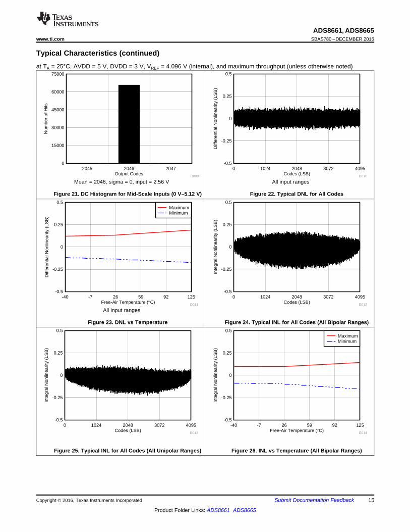
Typical Characteristics (continued)at TA = 25°C, AVDD = 5 V, DVDD = 3 V, VREF = 4.096 V (internal), and maximum throughput (unless otherwise noted)
Mean = 2046, sigma = 0, input = 0 V
Figure 15. DC Histogram for Mid-Scale Inputs (±6.144 V)
Mean = 2046, sigma = 0, input = 0 V
Figure 16. DC Histogram for Mid-Scale Inputs (±5.12 V)
Mean = 2046, sigma = 0, input = 0 V
Figure 17. DC Histogram for Mid-Scale Inputs(±2.56 V)
Mean = 2049, sigma = 0, input = 6.144 V
Figure 18. DC Histogram for Mid-Scale Inputs(0 V–12.288 V)
Mean = 2045, sigma = 0, input = 5.12 V
Figure 19. DC Histogram for Mid-Scale Inputs(0 V–10.24 V)
Mean = 2045, sigma = 0, input = 3.072 V
Figure 20. DC Histogram for Mid-Scale Inputs(0 V–6.144 V)
Codes (LSB)
Inte
gral
Non
linea
rity
(LS
B)
0 1024 2048 3072 4095-0.5
-0.25
0
0.25
0.5
D013Free-Air Temperature (qC)
Inte
gral
Non
linea
rity
(LS
B)
-40 -7 26 59 92 125-0.5
-0.25
0
0.25
0.5
D014
MaximumMinimum
Free-Air Temperature (qC)
Diff
eren
tial N
onlin
earit
y (L
SB
)
-40 -7 26 59 92 125-0.5
-0.25
0
0.25
0.5
D011
MaximumMinimum
Codes (LSB)
Inte
gral
Non
linea
rity
(LS
B)
0 1024 2048 3072 4095-0.5
-0.25
0
0.25
0.5
D012
Output Codes
Num
ber
of H
its
0
15000
30000
45000
60000
75000
2045 2046 2047
D009Codes (LSB)
Diff
eren
tial N
onlin
earit
y (L
SB
)
0 1024 2048 3072 4095-0.5
-0.25
0
0.25
0.5
D010
15
ADS8661, ADS8665www.ti.com SBAS780 –DECEMBER 2016
Product Folder Links: ADS8661 ADS8665
Submit Documentation FeedbackCopyright © 2016, Texas Instruments Incorporated
Typical Characteristics (continued)at TA = 25°C, AVDD = 5 V, DVDD = 3 V, VREF = 4.096 V (internal), and maximum throughput (unless otherwise noted)
Mean = 2046, sigma = 0, input = 2.56 V
Figure 21. DC Histogram for Mid-Scale Inputs (0 V–5.12 V)
All input ranges
Figure 22. Typical DNL for All Codes
All input ranges
Figure 23. DNL vs Temperature Figure 24. Typical INL for All Codes (All Bipolar Ranges)
Figure 25. Typical INL for All Codes (All Unipolar Ranges) Figure 26. INL vs Temperature (All Bipolar Ranges)

Gain Drift (ppm/ºC)
Num
ber
of U
nits
0
5
10
15
20
25
0 0.5 1 1.5 2 2.5 3 3.5 4 4.5 5
D039 Source Resistance (:)
Gai
n E
rror
(%
FS
R)
0 2000 4000 6000 8000 10000-0.1
0
0.1
0.2
0.3
0.4
0.5
0.6
0.7
0.8
0.9
1
1.1
D040
± 12.288 V± 10.24 V± 6.144 V± 5.12 V± 2.56 V0-12.288 V0-10.24 V0-6.144 V0-5.12 V
Offset Drift (ppm/ºC)
Num
ber
of D
evic
es
0
2.5
5
7.5
10
12.5
0 0.2 0.4 0.6 0.8 1 1.2 1.4 1.6 1.8 2.0 2.2 2.4 2.6 2.8 3
D037 Free-Air Temperature (0C)
Gai
n E
rror
(%
FS
R)
-40 -7 26 59 92 125-0.025
-0.015
-0.005
0.005
0.015
0.025
D038
± 12.288 V± 10.24 V± 6.144 V
± 5.12 V± 2.56 V0-12.288 V
0-10.24 V0-6.144 V0-5.12 V
Free-Air Temperature (0C)
Offs
et E
rror
(m
V)
-40 -7 26 59 92 125-1
-0.75
-0.5
-0.25
0
0.25
0.5
0.75
1
D036
± 12.288 V± 10.24 V± 6.144 V
± 5.12 V± 2.56 V0-12.288 V
0-10.24 V0-6.144 V0-5.12 V
Free-Air Temperature (qC)
Inte
gral
Non
linea
rity
(LS
B)
-40 -7 26 59 92 125-0.5
-0.25
0
0.25
0.5
D015
MaximumMinimum
16
ADS8661, ADS8665SBAS780 –DECEMBER 2016 www.ti.com
Product Folder Links: ADS8661 ADS8665
Submit Documentation Feedback Copyright © 2016, Texas Instruments Incorporated
Typical Characteristics (continued)at TA = 25°C, AVDD = 5 V, DVDD = 3 V, VREF = 4.096 V (internal), and maximum throughput (unless otherwise noted)
Figure 27. INL vs Temperature (All Unipolar Ranges) Figure 28. Offset Error vsTemperature Across Input Ranges
Figure 29. Typical Histogram for Offset Drift Figure 30. Gain Error vs Temperature Across Input Ranges
Figure 31. Typical Histogram for Gain Error Drift Figure 32. Gain Error vs External Resistance (REXT)
Input Frequency (Hz)
Sig
nal-t
o-N
oise
+ D
isto
rtio
n R
atio
(dB
)
70
71
72
73
74
100 1k 10k
D020
± 12.288 V± 10.24 V± 6.144 V± 5.12 V± 2.56 V0-12.288 V0-10.24 V0-6.144 V0-5.12 V
Free-AirTemperature (qC)
Sig
nal-t
o-N
oise
+ D
isto
rtio
n R
atio
(dB
)
-40 -7 26 59 92 12570
71
72
73
74
D021
± 12.288 V± 10.24 V± 6.144 V± 5.12 V± 2.56 V
0-12.288 V0-10.24 V0-6.144 V0-5.12 V
Input Frequency (Hz)
Sig
nal-t
o-N
oise
Rat
io (
dB)
72
72.5
73
73.5
74
100 1k 10k
D018
± 12.288 V± 10.24 V± 6.144 V± 5.12 V± 2.56 V
0-12.288 V0-10.24 V0-6.144 V0-5.12 V
Free-Air Temperature (qC)
Sig
nal-t
o-N
oise
Rat
io (
dB)
-40 -7 26 59 92 12572
72.5
73
73.5
74
D019
± 12.288 V± 10.24 V± 6.144 V± 5.12 V± 2.56 V
0-12.288 V0-10.24 V0-6.144 V0-5.12 V
Input Frequency (Hz)
Am
plitu
de (
dB)
0 125000 250000 375000 500000 625000-180
-150
-120
-90
-60
-30
0
D016Input Frequency (Hz)
Am
plitu
de (
dB)
0 50000 100000 150000 200000 250000-180
-150
-120
-90
-60
-30
0
D017
17
ADS8661, ADS8665www.ti.com SBAS780 –DECEMBER 2016
Product Folder Links: ADS8661 ADS8665
Submit Documentation FeedbackCopyright © 2016, Texas Instruments Incorporated
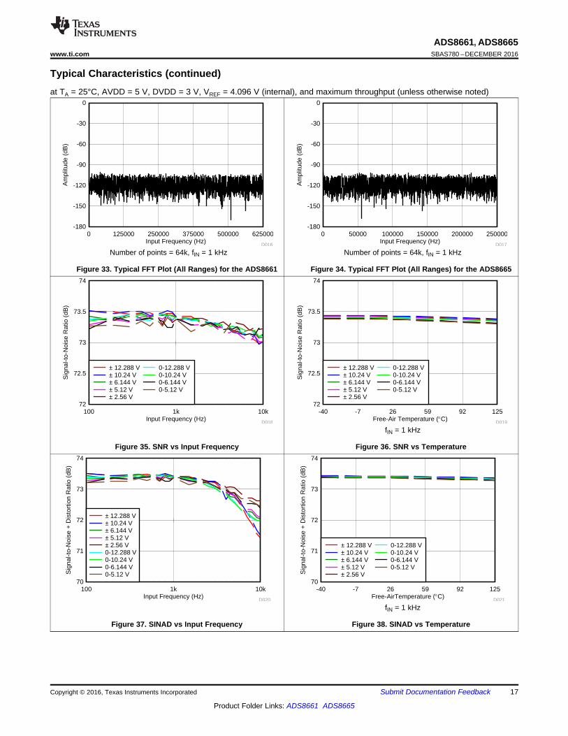
Typical Characteristics (continued)at TA = 25°C, AVDD = 5 V, DVDD = 3 V, VREF = 4.096 V (internal), and maximum throughput (unless otherwise noted)
Number of points = 64k, fIN = 1 kHz
Figure 33. Typical FFT Plot (All Ranges) for the ADS8661
Number of points = 64k, fIN = 1 kHz
Figure 34. Typical FFT Plot (All Ranges) for the ADS8665
Figure 35. SNR vs Input Frequency
fIN = 1 kHz
Figure 36. SNR vs Temperature
Figure 37. SINAD vs Input Frequency
fIN = 1 kHz
Figure 38. SINAD vs Temperature

Free-Air Temperature (0C)
I AV
DD S
tand
by (
mA
)
-40 -7 26 59 92 1252.4
2.5
2.6
2.7
2.8
D067
± 12.288 V± 10.24 V± 6.144 V
± 5.12 V± 2.56 V0-12.288 V
0-10.24 V0-6.144 V0-5.12 V
Free-Air Temperature (qC)
I AV
DD S
tatic
(m
A)
-40 -7 26 59 92 1252
2.5
3
3.5
4
D025
Free-Air Temperature (qC)
I AV
DD D
ynam
ic (
mA
)
-40 -7 26 59 92 1251
2
3
4
5
6
7
8
9
D024
ADS8661ADS8665
Throughput (ksps)
I AV
DD C
urre
nt (
mA
)
0 250 500 750 1000 12503.5
4
4.5
5
5.5
6
6.5
7
D026
Input Frequency (Hz)
Tot
al H
arm
onic
Dis
tort
ion
Rat
io (
dB)
-120
-110
-100
-90
-80
100 1k 10k
D022
± 12.288 V± 10.24 V± 6.144 V± 5.12 V± 2.56 V
0-12.288 V0-10.24 V0-6.144 V0-5.12 V
Free-AirTemperature (qC)
Tot
al H
arm
onic
Dis
tort
ion
(dB
)
-40 -7 26 59 92 125-120
-110
-100
-90
-80
D023
± 12.288 V± 10.24 V± 6.144 V
± 5.12 V± 2.56 V0-12.288 V
0-10.24 V0-6.144 V0-5.12 V
18
ADS8661, ADS8665SBAS780 –DECEMBER 2016 www.ti.com
Product Folder Links: ADS8661 ADS8665
Submit Documentation Feedback Copyright © 2016, Texas Instruments Incorporated
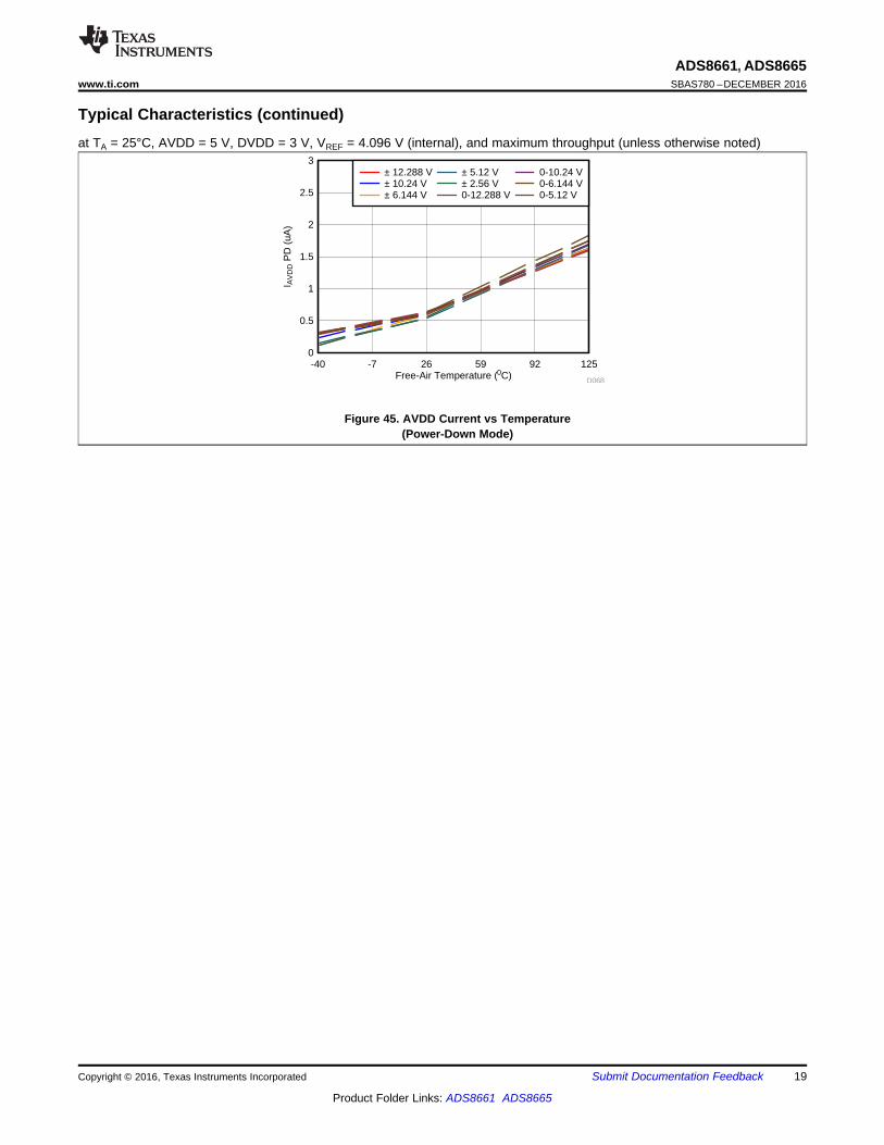
Typical Characteristics (continued)at TA = 25°C, AVDD = 5 V, DVDD = 3 V, VREF = 4.096 V (internal), and maximum throughput (unless otherwise noted)
Figure 39. THD vs Input Frequency
fIN = 1 kHz
Figure 40. THD vs Temperature
Figure 41. AVDD Current vs Temperature Figure 42. AVDD Current vs Throughput
Figure 43. AVDD Current vs Temperature(During Sampling)
Figure 44. AVDD Current vs Temperature(Standby Mode)
Free-Air Temperature (0C)
I AV
DD P
D (
uA)
-40 -7 26 59 92 1250
0.5
1
1.5
2
2.5
3
D068
± 12.288 V± 10.24 V± 6.144 V
± 5.12 V± 2.56 V0-12.288 V
0-10.24 V0-6.144 V0-5.12 V
19
ADS8661, ADS8665www.ti.com SBAS780 –DECEMBER 2016
Product Folder Links: ADS8661 ADS8665
Submit Documentation FeedbackCopyright © 2016, Texas Instruments Incorporated
Typical Characteristics (continued)at TA = 25°C, AVDD = 5 V, DVDD = 3 V, VREF = 4.096 V (internal), and maximum throughput (unless otherwise noted)
Figure 45. AVDD Current vs Temperature(Power-Down Mode)
Oscillator
CONVST/CS
PGA
1 M:
OVP
1 M:
OVP
2nd-OrderLPF
ADCDriver
VBIAS
AIN_P
AIN_GND
4.096-VReference
REFGNDDGNDAGND
DVDDAVDD
Digital Logicand Interface
REFIO
REFCAP
SCLK
SDI
SDO
12-BitSAR ADC
ADS866x
Copyright © 2016, Texas Instruments Incorporated
20
ADS8661, ADS8665SBAS780 –DECEMBER 2016 www.ti.com
Product Folder Links: ADS8661 ADS8665
Submit Documentation Feedback Copyright © 2016, Texas Instruments Incorporated
7 Detailed Description
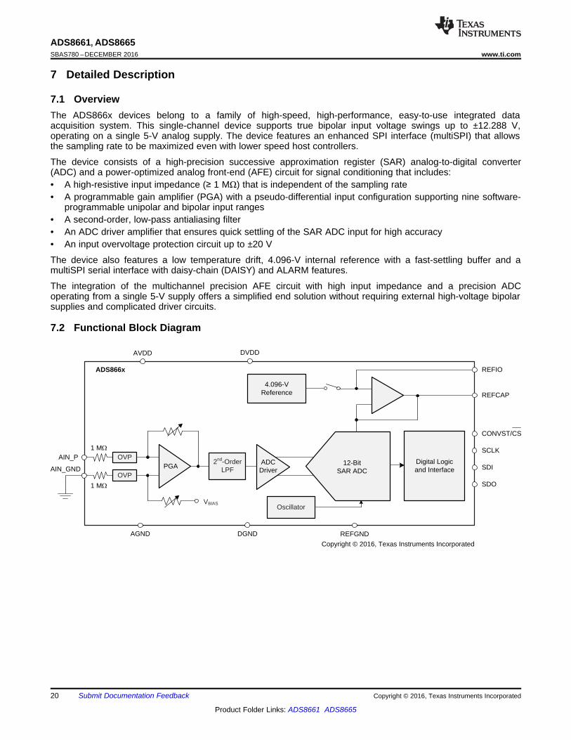
7.1 OverviewThe ADS866x devices belong to a family of high-speed, high-performance, easy-to-use integrated dataacquisition system. This single-channel device supports true bipolar input voltage swings up to ±12.288 V,operating on a single 5-V analog supply. The device features an enhanced SPI interface (multiSPI) that allowsthe sampling rate to be maximized even with lower speed host controllers.
The device consists of a high-precision successive approximation register (SAR) analog-to-digital converter(ADC) and a power-optimized analog front-end (AFE) circuit for signal conditioning that includes:• A high-resistive input impedance (≥ 1 MΩ) that is independent of the sampling rate• A programmable gain amplifier (PGA) with a pseudo-differential input configuration supporting nine software-
programmable unipolar and bipolar input ranges• A second-order, low-pass antialiasing filter• An ADC driver amplifier that ensures quick settling of the SAR ADC input for high accuracy• An input overvoltage protection circuit up to ±20 V
The device also features a low temperature drift, 4.096-V internal reference with a fast-settling buffer and amultiSPI serial interface with daisy-chain (DAISY) and ALARM features.
The integration of the multichannel precision AFE circuit with high input impedance and a precision ADCoperating from a single 5-V supply offers a simplified end solution without requiring external high-voltage bipolarsupplies and complicated driver circuits.
7.2 Functional Block Diagram
PGA
1 M:
OVP
1 M:
OVP
2nd-OrderLPF
ADCDriver
VB
ADCAIN_P
AIN_GND
CONVST/CSSCLKSDISDO
21
ADS8661, ADS8665www.ti.com SBAS780 –DECEMBER 2016
Product Folder Links: ADS8661 ADS8665
Submit Documentation FeedbackCopyright © 2016, Texas Instruments Incorporated
7.3 Feature Description
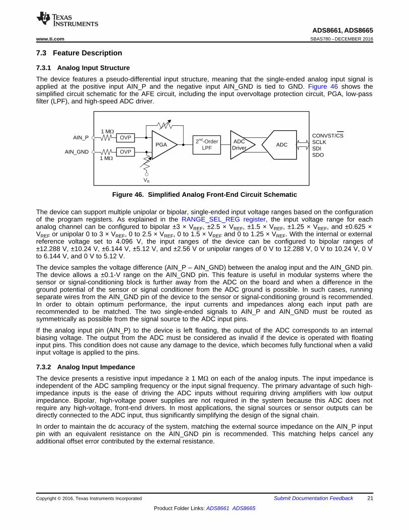
7.3.1 Analog Input StructureThe device features a pseudo-differential input structure, meaning that the single-ended analog input signal isapplied at the positive input AIN_P and the negative input AIN_GND is tied to GND. Figure 46 shows thesimplified circuit schematic for the AFE circuit, including the input overvoltage protection circuit, PGA, low-passfilter (LPF), and high-speed ADC driver.
Figure 46. Simplified Analog Front-End Circuit Schematic
The device can support multiple unipolar or bipolar, single-ended input voltage ranges based on the configurationof the program registers. As explained in the RANGE_SEL_REG register, the input voltage range for eachanalog channel can be configured to bipolar ±3 × VREF, ±2.5 × VREF, ±1.5 × VREF, ±1.25 × VREF, and ±0.625 ×VREF or unipolar 0 to 3 × VREF, 0 to 2.5 × VREF, 0 to 1.5 × VREF and 0 to 1.25 × VREF. With the internal or externalreference voltage set to 4.096 V, the input ranges of the device can be configured to bipolar ranges of±12.288 V, ±10.24 V, ±6.144 V, ±5.12 V, and ±2.56 V or unipolar ranges of 0 V to 12.288 V, 0 V to 10.24 V, 0 Vto 6.144 V, and 0 V to 5.12 V.
The device samples the voltage difference (AIN_P – AIN_GND) between the analog input and the AIN_GND pin.The device allows a ±0.1-V range on the AIN_GND pin. This feature is useful in modular systems where thesensor or signal-conditioning block is further away from the ADC on the board and when a difference in theground potential of the sensor or signal conditioner from the ADC ground is possible. In such cases, runningseparate wires from the AIN_GND pin of the device to the sensor or signal-conditioning ground is recommended.In order to obtain optimum performance, the input currents and impedances along each input path arerecommended to be matched. The two single-ended signals to AIN_P and AIN_GND must be routed assymmetrically as possible from the signal source to the ADC input pins.
If the analog input pin (AIN_P) to the device is left floating, the output of the ADC corresponds to an internalbiasing voltage. The output from the ADC must be considered as invalid if the device is operated with floatinginput pins. This condition does not cause any damage to the device, which becomes fully functional when a validinput voltage is applied to the pins.
7.3.2 Analog Input ImpedanceThe device presents a resistive input impedance ≥ 1 MΩ on each of the analog inputs. The input impedance isindependent of the ADC sampling frequency or the input signal frequency. The primary advantage of such high-impedance inputs is the ease of driving the ADC inputs without requiring driving amplifiers with low outputimpedance. Bipolar, high-voltage power supplies are not required in the system because this ADC does notrequire any high-voltage, front-end drivers. In most applications, the signal sources or sensor outputs can bedirectly connected to the ADC input, thus significantly simplifying the design of the signal chain.
In order to maintain the dc accuracy of the system, matching the external source impedance on the AIN_P inputpin with an equivalent resistance on the AIN_GND pin is recommended. This matching helps cancel anyadditional offset error contributed by the external resistance.

VOUT
V+
V±
+
VB
AVDD
GND
AIN_P
AIN_GND
1 M�
1 M�
RDC
RFB
0 V
VP+
VP- RS
ESD
D1p
D2n
RS
AVDD
AVDDD2p
D1n
ESD
22
ADS8661, ADS8665SBAS780 –DECEMBER 2016 www.ti.com
Product Folder Links: ADS8661 ADS8665
Submit Documentation Feedback Copyright © 2016, Texas Instruments Incorporated
Feature Description (continued)
(1) GND = 0 V, AIN_GND = 0 V, |VRANGE| is the maximum input voltage for any selected input range, and |VOVP| is the break-down voltagefor the internal OVP circuit. Assume that RS is approximately 0 Ω.
7.3.3 Input Protection CircuitThe device features an internal overvoltage protection (OVP) circuit on each of the analog inputs. Use theinternal protection circuit only as a secondary protection scheme. The external protection devices in the endapplication are highly recommended to be used to protect against surges, electrostatic discharge (ESD), andelectrical fast transient (EFT) conditions. A conceptual block diagram of the internal OVP circuit is shown inFigure 47.
Figure 47. Input Overvoltage Protection Circuit Schematic
As shown in Figure 47, the combination of the 1-MΩ (or, 1.2 MΩ for appropriate input ranges) input resistorsalong with the PGA gain-setting resistors RFB and RDC limit the current flowing into the input pin. A combinationof anti-parallel diodes, D1 and D2 are added to protect the internal circuitry and set the overvoltage protectionlimits.
Table 1 explains the various operating conditions for the device when powered on. This table indicates that whenthe device is properly powered up (AVDD = 5 V) or offers a low impedance of < 30 kΩ, the internal overvoltageprotection circuit can withstand up to ±20 V on the analog input pins.
Table 1. Input Overvoltage Protection Limits When AVDD = 5 V or Offers a Low Impedance of < 30 kΩ (1)
INPUT CONDITION(VOVP = ±20 V) TEST
CONDITIONADC
OUTPUT COMMENTSCONDITION RANGE
|VIN| < |VRANGE| Within operating range All inputranges Valid Device functions as per data sheet specifications.
|VRANGE| < |VIN| < |VOVP| Beyond operating range butwithin overvoltage range
All inputranges Saturated ADC output is saturated, but device is internally protected
(not recommended for extended time).
|VIN| > |VOVP| Beyond overvoltage range All inputranges Saturated This usage condition can cause irreversible damage to the
device.
Input voltage (V)
Inpu
t Cur
rent
(uA
)
-30 -24 -18 -12 -6 0 6 12 18 24 30-30
-20
-10
0
10
20
30
D005Input voltage (V)
Inpu
t Cur
rent
(uA
)
-20 -16 -12 -8 -4 0 4 8 12 16 20-24
-18
-12
-6
0
6
12
18
24
D006
23
ADS8661, ADS8665www.ti.com SBAS780 –DECEMBER 2016
Product Folder Links: ADS8661 ADS8665
Submit Documentation FeedbackCopyright © 2016, Texas Instruments Incorporated
(1) AVDD = floating, GND = 0 V, AIN_GND = 0 V, |VRANGE| is the maximum input voltage for any selected input range, and |VOVP| is thebreak-down voltage for the internal OVP circuit. Assume that RS is approximately 0 Ω.
The results indicated in Table 1 are based on an assumption that the analog input pin is driven by a very lowimpedance source (RS is approximately 0 Ω). However, if the source driving the input has higher impedance, thecurrent flowing through the protection diodes reduces further, thereby increasing the OVP voltage range. Notethat higher source impedances result in gain errors and contribute to overall system noise performance.
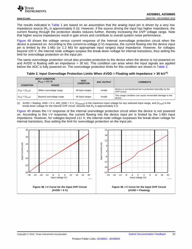
Figure 48 shows the voltage versus current response of the internal overvoltage protection circuit when thedevice is powered on. According to this current-to-voltage (I-V) response, the current flowing into the device inputpin is limited by the 1-MΩ (or 1.2 MΩ for appropriate input ranges) input impedance. However, for voltagesbeyond ±20 V, the internal node voltages surpass the break-down voltage for internal transistors, thus setting thelimit for overvoltage protection on the input pin.
The same overvoltage protection circuit also provides protection to the device when the device is not powered onand AVDD is floating with an impedance > 30 kΩ. This condition can arise when the input signals are appliedbefore the ADC is fully powered on. The overvoltage protection limits for this condition are shown in Table 2.
Table 2. Input Overvoltage Protection Limits When AVDD = Floating with Impedance > 30 kΩ (1)
INPUT CONDITION(VOVP = ±11 V) TEST
CONDITION ADC OUTPUT COMMENTSCONDITION RANGE
|VIN| < |VOVP| Within overvoltage range All input ranges Invalid Device is not functional but is protected internally by theOVP circuit.
|VIN| > |VOVP| Beyond overvoltage range All input ranges Invalid This usage condition can cause irreversible damage to thedevice.
Figure 49 shows the I-V response of the internal overvoltage protection circuit when the device is not poweredon. According to this I-V response, the current flowing into the device input pin is limited by the 1-MΩ inputimpedance. However, for voltages beyond ±11 V, the internal node voltage surpasses the break-down voltage forinternal transistors, thus setting the limit for overvoltage protection on the input pin.
Figure 48. I-V Curve for the Input OVP Circuit(AVDD = 5 V)
Figure 49. I-V Curve for the Input OVP Circuit(AVDD = Floating)
Input Frequency (Hz)
Mag
nitu
de (
dB)
-15
-12
-9
-6
-3
0
3
10 100 1k 10k 100k
D058
±12.288 V±10.24 V±6.144 V±5.12 V±2.56 V0-12.288 V0-10.24 V0-6.144 V0-5.12 V
Input Frequency (Hz)
Pha
se (
Deg
ree)
-135
-90
-45
0
45
10 100 1k 10k 100k
D059
± 12.288 V± 10.24 V± 6.144 V± 5.12 V± 2.56 V0-12.288 V0-10.24 V0-6.144 V0-5.12 V
24
ADS8661, ADS8665SBAS780 –DECEMBER 2016 www.ti.com
Product Folder Links: ADS8661 ADS8665
Submit Documentation Feedback Copyright © 2016, Texas Instruments Incorporated
7.3.4 Programmable Gain Amplifier (PGA)The device features a programmable gain amplifier (PGA) as part of the analog signal-conditioning circuit thatconverts the original single-ended input signal into a fully-differential signal to drive the internal SAR ADC. ThePGA also adjusts the common-mode level of the input signal before feeding it into the SAR ADC to ensuremaximum usage of the ADC input dynamic range. Depending on the range of the input signal, the PGA gain canbe adjusted by setting the RANGE_SEL[3:0] bits in the configuration register (see the RANGE_SEL_REGregister). The default or power-on state for the RANGE_SEL[3:0] bits is 0000, corresponding to an input signalrange of ±3 × VREF. Table 3 lists the various configurations of the RANGE_SEL[3:0] bits for the different analoginput voltage ranges.
The PGA uses a precisely-matched network of resistors for multiple gain configurations. Matching between theseresistors is accurately trimmed to keep the overall gain error low across all input ranges.
Table 3. Input Range Selection Bits Configuration
ANALOG INPUT RANGERANGE_SEL[3:0]
BIT 3 BIT 2 BIT 1 BIT 0±3 × VREF 0 0 0 0
±2.5 × VREF 0 0 0 1±1.5 × VREF 0 0 1 0±1.25 × VREF 0 0 1 1±0.625 × VREF 0 1 0 0
0–3 × VREF 1 0 0 00–2.5 × VREF 1 0 0 10–1.5 × VREF 1 0 1 00–1.25 × VREF 1 0 1 1
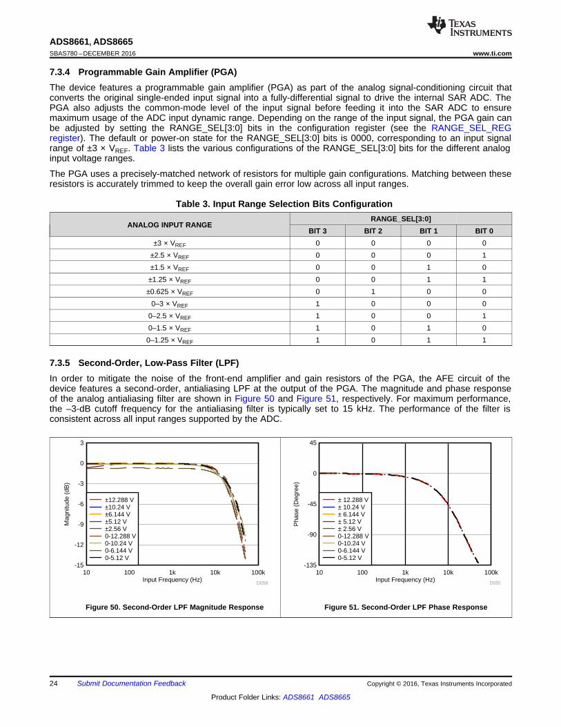
7.3.5 Second-Order, Low-Pass Filter (LPF)In order to mitigate the noise of the front-end amplifier and gain resistors of the PGA, the AFE circuit of thedevice features a second-order, antialiasing LPF at the output of the PGA. The magnitude and phase responseof the analog antialiasing filter are shown in Figure 50 and Figure 51, respectively. For maximum performance,the –3-dB cutoff frequency for the antialiasing filter is typically set to 15 kHz. The performance of the filter isconsistent across all input ranges supported by the ADC.
Figure 50. Second-Order LPF Magnitude Response Figure 51. Second-Order LPF Phase Response

ADC
4.096 VREF
REFCAP
REFIO
AGND
10 PF
REFGND
4.7 PF
AVDD
1 PF
RANGE_SEL_REG[6] = 0(INTREF_DIS)
25
ADS8661, ADS8665www.ti.com SBAS780 –DECEMBER 2016
Product Folder Links: ADS8661 ADS8665
Submit Documentation FeedbackCopyright © 2016, Texas Instruments Incorporated
7.3.6 ADC DriverIn order to meet the performance of the device at the maximum sampling rate, the sample-and-hold capacitors atthe input of the ADC must be successfully charged and discharged during the acquisition time window. This driverequirement at the input of the ADC necessitates the use of a high-bandwidth, low-noise, and stable amplifierbuffer. Such an input driver is integrated in the front-end signal path of the analog input channel of the device.
7.3.7 ReferenceThe device can operate with either an internal voltage reference or an external voltage reference using theinternal buffer. The internal or external reference selection is determined by programming the INTREF_DIS bit ofthe RANGE_SEL_REG register. The internal reference source is enabled (INTREF_DIS = 0) by default afterreset or when the device powers up. The INTREF_DIS bit must be programmed to logic 1 to disable the internalreference source whenever an external reference source is used.
7.3.7.1 Internal ReferenceThe device features an internal reference source with a nominal output value of 4.096 V. In order to select theinternal reference, the INTREF_DIS bit of the RANGE_SEL_REG register must be programmed to logic 0. Whenthe internal reference is used, the REFIO pin becomes an output with the internal reference value. A 4.7-µF(minimum) decoupling capacitor is recommended to be placed between the REFIO pin and REFGND, as shownin Figure 52. The capacitor must be placed as close to the REFIO pin as possible. The output impedance of theinternal band-gap circuit creates a low-pass filter with this capacitor to band-limit the noise of the reference. Theuse of a smaller capacitor value allows higher reference noise in the system that can potentially degrade SNRand SINAD performance. The REFIO pin must not be used to drive external ac or dc loads because of limitedcurrent output capability. The REFIO pin can be used as a source if followed by a suitable op amp buffer (suchas the OPA320).
Figure 52. Device Connections for Using an Internal 4.096-V Reference
Error in REFIO Voltage (mV)
Num
ber
of D
evic
es
00.5
11.5
22.5
33.5
44.5
55.5
66.5
7
-7 -6 -5 -4 -3 -2 -1 0 1
D070
REFIO Voltage (V)
Num
ber
of D
evic
es
0
100
200
300
400
500
600
700
800
900
1000
4.094 4.0945 4.095 4.0955 4.096 4.0965 4.097 4.0975 4.098
D060
26
ADS8661, ADS8665SBAS780 –DECEMBER 2016 www.ti.com
Product Folder Links: ADS8661 ADS8665
Submit Documentation Feedback Copyright © 2016, Texas Instruments Incorporated
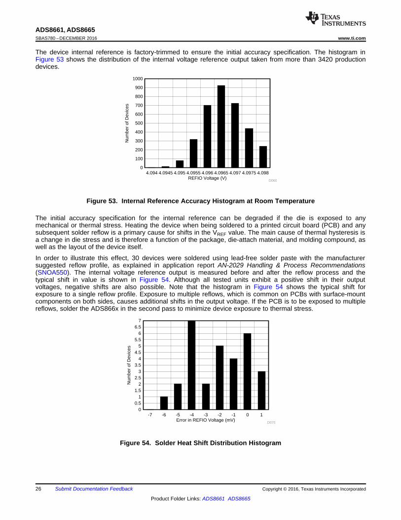
The device internal reference is factory-trimmed to ensure the initial accuracy specification. The histogram inFigure 53 shows the distribution of the internal voltage reference output taken from more than 3420 productiondevices.
Figure 53. Internal Reference Accuracy Histogram at Room Temperature
The initial accuracy specification for the internal reference can be degraded if the die is exposed to anymechanical or thermal stress. Heating the device when being soldered to a printed circuit board (PCB) and anysubsequent solder reflow is a primary cause for shifts in the VREF value. The main cause of thermal hysteresis isa change in die stress and is therefore a function of the package, die-attach material, and molding compound, aswell as the layout of the device itself.
In order to illustrate this effect, 30 devices were soldered using lead-free solder paste with the manufacturersuggested reflow profile, as explained in application report AN-2029 Handling & Process Recommendations(SNOA550). The internal voltage reference output is measured before and after the reflow process and thetypical shift in value is shown in Figure 54. Although all tested units exhibit a positive shift in their outputvoltages, negative shifts are also possible. Note that the histogram in Figure 54 shows the typical shift forexposure to a single reflow profile. Exposure to multiple reflows, which is common on PCBs with surface-mountcomponents on both sides, causes additional shifts in the output voltage. If the PCB is to be exposed to multiplereflows, solder the ADS866x in the second pass to minimize device exposure to thermal stress.
Figure 54. Solder Heat Shift Distribution Histogram
REFIO Drift (ppm/ºC)
Num
ber
of D
evic
es
0
2
4
6
8
10
12
14
3.1 3.5 3.9 4.3 4.7 5.1 5.5 5.9 6.3 6.7 7.1
D062REFIO Drift (ppm/ºC)
Num
ber
of D
evic
es
0
2
4
6
8
2.2 3 3.8 4.6 5.4 6.2 7 7.8 8.6 9.4 10.2 11
D622
Free-Air Temperature (0C)
RE
FIO
Vol
tage
(V
) -
TS
SO
P
-40 -7 26 59 92 1254.09
4.091
4.092
4.093
4.094
4.095
4.096
4.097
4.098
4.099
4.1
D061
AVDD = 5.25 VAVDD = 5 VAVDD = 4.75 V
Free-Air Temperature (0C)
RE
FIO
Vol
tage
(V
) -
QF
N
-40 -7 26 59 92 1254.089
4.09
4.091
4.092
4.093
4.094
4.095
4.096
4.097
D612
AVDD = 5.25 VAVDD = 5 VAVDD = 4.75 V
27
ADS8661, ADS8665www.ti.com SBAS780 –DECEMBER 2016
Product Folder Links: ADS8661 ADS8665
Submit Documentation FeedbackCopyright © 2016, Texas Instruments Incorporated
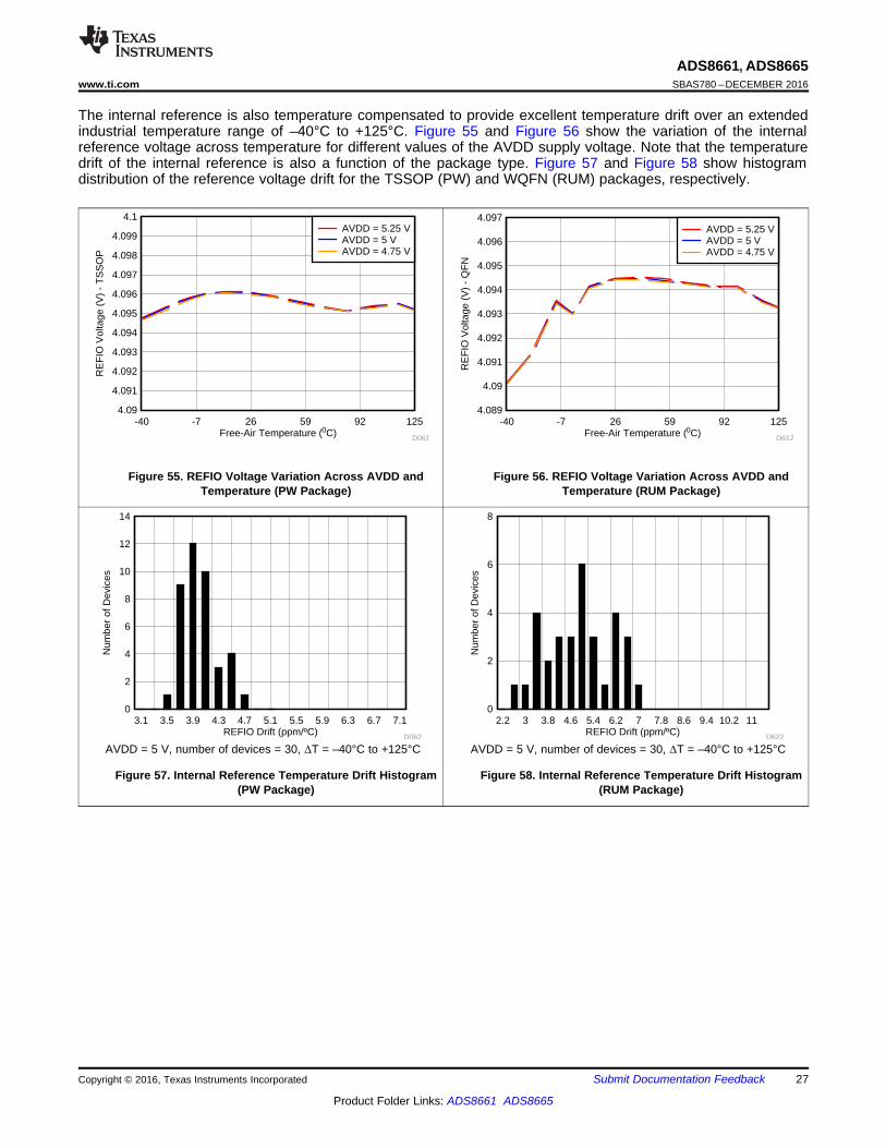
The internal reference is also temperature compensated to provide excellent temperature drift over an extendedindustrial temperature range of –40°C to +125°C. Figure 55 and Figure 56 show the variation of the internalreference voltage across temperature for different values of the AVDD supply voltage. Note that the temperaturedrift of the internal reference is also a function of the package type. Figure 57 and Figure 58 show histogramdistribution of the reference voltage drift for the TSSOP (PW) and WQFN (RUM) packages, respectively.
Figure 55. REFIO Voltage Variation Across AVDD andTemperature (PW Package)
Figure 56. REFIO Voltage Variation Across AVDD andTemperature (RUM Package)
AVDD = 5 V, number of devices = 30, ΔT = –40°C to +125°C
Figure 57. Internal Reference Temperature Drift Histogram(PW Package)
AVDD = 5 V, number of devices = 30, ΔT = –40°C to +125°C
Figure 58. Internal Reference Temperature Drift Histogram(RUM Package)
ADC
4.096 VREF
REFCAP
REFIO
AGND
10 PF
REFGND
CREF
AVDD
REF5040(See the device datasheet for a detailed pin configuration.)
AVDD
OUT
1 PF
RANGE_SEL_REG[6] = 1(INTREF_DIS)
28
ADS8661, ADS8665SBAS780 –DECEMBER 2016 www.ti.com
Product Folder Links: ADS8661 ADS8665
Submit Documentation Feedback Copyright © 2016, Texas Instruments Incorporated
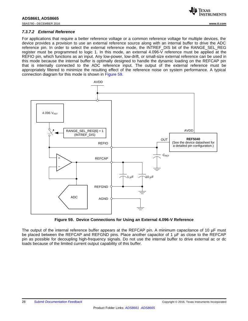
7.3.7.2 External ReferenceFor applications that require a better reference voltage or a common reference voltage for multiple devices, thedevice provides a provision to use an external reference source along with an internal buffer to drive the ADCreference pin. In order to select the external reference mode, the INTREF_DIS bit of the RANGE_SEL_REGregister must be programmed to logic 1. In this mode, an external 4.096-V reference must be applied at theREFIO pin, which functions as an input. Any low-power, low-drift, or small-size external reference can be used inthis mode because the internal buffer is optimally designed to handle the dynamic loading on the REFCAP pinthat is internally connected to the ADC reference input. The output of the external reference must beappropriately filtered to minimize the resulting effect of the reference noise on system performance. A typicalconnection diagram for this mode is shown in Figure 59.
Figure 59. Device Connections for Using an External 4.096-V Reference
The output of the internal reference buffer appears at the REFCAP pin. A minimum capacitance of 10 µF mustbe placed between the REFCAP and REFGND pins. Place another capacitor of 1 µF as close to the REFCAPpin as possible for decoupling high-frequency signals. Do not use the internal buffer to drive external ac or dcloads because of the limited current output capability of this buffer.
Free-Air Temperature (0C)
RE
FC
AP
Vol
tage
(V
) -
QF
N
-40 -7 26 59 92 1254.09
4.091
4.092
4.093
4.094
4.095
4.096
4.097
4.098
D632
AVDD = 5.25 VAVDD = 5 VAVDD = 4.75 V
REFCAP Drift (ppm/ºC)
Num
ber
of D
evic
es
0
2
4
6
8
10
12
14
16
18
0.2 0.4 0.6 0.8 1.0 1.2 1.4 1.6 1.8 2.0
D642
Free-Air Temperature (0C)
RE
FC
AP
Vol
tage
(V
) -
TS
SO
P
-40 -7 26 59 92 1254.09
4.091
4.092
4.093
4.094
4.095
4.096
4.097
4.098
4.099
4.1
D063
AVDD = 5.25 VAVDD = 5 VAVDD = 4.75 V
REFCAP Drift (ppm/ºC)
Num
ber
of D
evic
es
0
4
8
12
16
20
24
0.2 0.4 0.6 0.8 1.0 1.2 1.4 1.6 1.8 2.0
D064
29
ADS8661, ADS8665www.ti.com SBAS780 –DECEMBER 2016
Product Folder Links: ADS8661 ADS8665
Submit Documentation FeedbackCopyright © 2016, Texas Instruments Incorporated
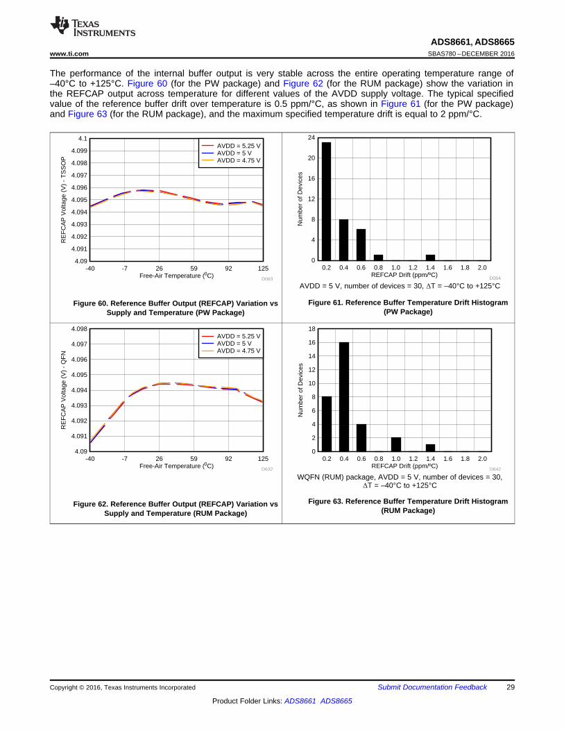
The performance of the internal buffer output is very stable across the entire operating temperature range of–40°C to +125°C. Figure 60 (for the PW package) and Figure 62 (for the RUM package) show the variation inthe REFCAP output across temperature for different values of the AVDD supply voltage. The typical specifiedvalue of the reference buffer drift over temperature is 0.5 ppm/°C, as shown in Figure 61 (for the PW package)and Figure 63 (for the RUM package), and the maximum specified temperature drift is equal to 2 ppm/°C.
Figure 60. Reference Buffer Output (REFCAP) Variation vsSupply and Temperature (PW Package)
AVDD = 5 V, number of devices = 30, ΔT = –40°C to +125°C
Figure 61. Reference Buffer Temperature Drift Histogram(PW Package)
Figure 62. Reference Buffer Output (REFCAP) Variation vsSupply and Temperature (RUM Package)
WQFN (RUM) package, AVDD = 5 V, number of devices = 30,ΔT = –40°C to +125°C
Figure 63. Reference Buffer Temperature Drift Histogram(RUM Package)
001h
FFFh
800h
FSR ± 1 LSBFSR / 21 LSB
AD
C O
utpu
t Cod
e
Analog Input(AIN_P ± AIN_GND)
NFS PFS
30
ADS8661, ADS8665SBAS780 –DECEMBER 2016 www.ti.com
Product Folder Links: ADS8661 ADS8665
Submit Documentation Feedback Copyright © 2016, Texas Instruments Incorporated
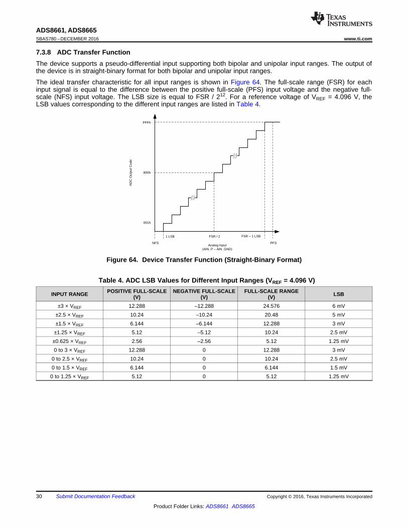
7.3.8 ADC Transfer FunctionThe device supports a pseudo-differential input supporting both bipolar and unipolar input ranges. The output ofthe device is in straight-binary format for both bipolar and unipolar input ranges.
The ideal transfer characteristic for all input ranges is shown in Figure 64. The full-scale range (FSR) for eachinput signal is equal to the difference between the positive full-scale (PFS) input voltage and the negative full-scale (NFS) input voltage. The LSB size is equal to FSR / 212. For a reference voltage of VREF = 4.096 V, theLSB values corresponding to the different input ranges are listed in Table 4.
Figure 64. Device Transfer Function (Straight-Binary Format)
Table 4. ADC LSB Values for Different Input Ranges (VREF = 4.096 V)
INPUT RANGE POSITIVE FULL-SCALE(V)
NEGATIVE FULL-SCALE(V)
FULL-SCALE RANGE(V) LSB
±3 × VREF 12.288 –12.288 24.576 6 mV±2.5 × VREF 10.24 –10.24 20.48 5 mV±1.5 × VREF 6.144 –6.144 12.288 3 mV±1.25 × VREF 5.12 –5.12 10.24 2.5 mV
±0.625 × VREF 2.56 –2.56 5.12 1.25 mV0 to 3 × VREF 12.288 0 12.288 3 mV
0 to 2.5 × VREF 10.24 0 10.24 2.5 mV0 to 1.5 × VREF 6.144 0 6.144 1.5 mV0 to 1.25 × VREF 5.12 0 5.12 1.25 mV
ADC Output
Input Alarm Threshold +/-
Hysteresis
+
S Q
QRAlarm Flag Read
Input Active Alarm Flag
Input Tripped Alarm Flag
Other Input Alarm
SDO
ALARM
ADC
ADCST Rising(End of Conversion)
AVDD Low Alarm
AVDD High Alarm
31
ADS8661, ADS8665www.ti.com SBAS780 –DECEMBER 2016
Product Folder Links: ADS8661 ADS8665
Submit Documentation FeedbackCopyright © 2016, Texas Instruments Incorporated
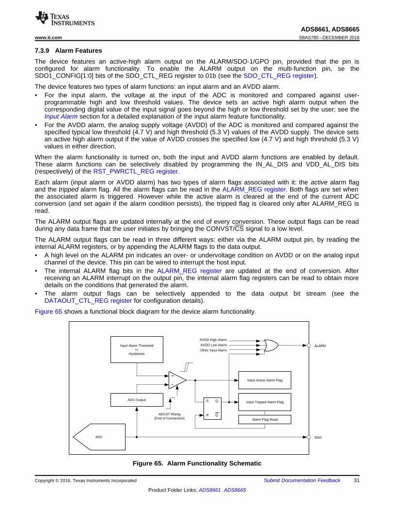
7.3.9 Alarm FeaturesThe device features an active-high alarm output on the ALARM/SDO-1/GPO pin, provided that the pin isconfigured for alarm functionality. To enable the ALARM output on the multi-function pin, se theSDO1_CONFIG[1:0] bits of the SDO_CTL_REG register to 01b (see the SDO_CTL_REG register).
The device features two types of alarm functions: an input alarm and an AVDD alarm.• For the input alarm, the voltage at the input of the ADC is monitored and compared against user-
programmable high and low threshold values. The device sets an active high alarm output when thecorresponding digital value of the input signal goes beyond the high or low threshold set by the user; see theInput Alarm section for a detailed explanation of the input alarm feature functionality.
• For the AVDD alarm, the analog supply voltage (AVDD) of the ADC is monitored and compared against thespecified typical low threshold (4.7 V) and high threshold (5.3 V) values of the AVDD supply. The device setsan active high alarm output if the value of AVDD crosses the specified low (4.7 V) and high threshold (5.3 V)values in either direction.
When the alarm functionality is turned on, both the input and AVDD alarm functions are enabled by default.These alarm functions can be selectively disabled by programming the IN_AL_DIS and VDD_AL_DIS bits(respectively) of the RST_PWRCTL_REG register.
Each alarm (input alarm or AVDD alarm) has two types of alarm flags associated with it: the active alarm flagand the tripped alarm flag. All the alarm flags can be read in the ALARM_REG register. Both flags are set whenthe associated alarm is triggered. However while the active alarm is cleared at the end of the current ADCconversion (and set again if the alarm condition persists), the tripped flag is cleared only after ALARM_REG isread.
The ALARM output flags are updated internally at the end of every conversion. These output flags can be readduring any data frame that the user initiates by bringing the CONVST/CS signal to a low level.
The ALARM output flags can be read in three different ways: either via the ALARM output pin, by reading theinternal ALARM registers, or by appending the ALARM flags to the data output.• A high level on the ALARM pin indicates an over- or undervoltage condition on AVDD or on the analog input
channel of the device. This pin can be wired to interrupt the host input.• The internal ALARM flag bits in the ALARM_REG register are updated at the end of conversion. After
receiving an ALARM interrupt on the output pin, the internal alarm flag registers can be read to obtain moredetails on the conditions that generated the alarm.
• The alarm output flags can be selectively appended to the data output bit stream (see theDATAOUT_CTL_REG register for configuration details).
Figure 65 shows a functional block diagram for the device alarm functionality.
Figure 65. Alarm Functionality Schematic

Ala
rm T
hres
hold
ADC Output
H_ALARM On
H_ALARM Off
(T ± H ± 1) (T) ADC Output
L_ALARM Off
L_ALARM On
(T + H + 1)(T)A
larm
Thr
esho
ld
32
ADS8661, ADS8665SBAS780 –DECEMBER 2016 www.ti.com
Product Folder Links: ADS8661 ADS8665
Submit Documentation Feedback Copyright © 2016, Texas Instruments Incorporated
7.3.9.1 Input AlarmThe device features a high and a low alarm on the analog input. The alarms corresponding to the input signalhave independently-programmable thresholds and a common hysteresis setting that can be controlled throughthe ALARM_H_TH_REG and ALARM_L_TH_REG registers.
The device sets the input high alarm when the digital output exceeds the high alarm upper limit [high alarmthreshold (T)]. The alarm resets when the digital output is less than or equal to the high alarm lower limit [highalarm (T) – H – 1). This function is shown in Figure 66.
Similarly, the input low alarm is triggered when the digital output falls below the low alarm lower limit [low alarmthreshold (T)]. The alarm resets when the digital output is greater than or equal to the low alarm higher limit [lowalarm (T) + H + 1]. This function is shown in Figure 67.
Figure 66. High ALARM Hysteresis Figure 67. Low ALARM Hysteresis
7.3.9.2 AVDD AlarmThe device features a high and a low alarm on the analog voltage supply, AVDD. Unlike the input signal alarm,the AVDD alarm has fixed trip points that are set by design. The device features an internal analog comparatorthat constantly monitors the analog supply against the high and low threshold voltages. The high alarm is set ifAVDD exceeds a typical value of 5.3 V and the low alarm is asserted if AVDD drops below 4.7 V. This feature isspecially useful for debugging unusual device behavior caused by a glitch or brown-out condition on the analogAVDD supply.

Interface Module
Configuration Registers
RST
CONVST
CS
SCLK
ALARM/SDO-1/GPO
RVS
Digital Control Logic
Output Register (Data and Flags from Device)
Input Register
D31 D30 D1 D0
B31 B30 B1 B0
ADC
Command Processor
SCLK Counter
SDI
LSB LSB+1 MSB-1 MSB SDO-0
Unified Shift Register
33
ADS8661, ADS8665www.ti.com SBAS780 –DECEMBER 2016
Product Folder Links: ADS8661 ADS8665
Submit Documentation FeedbackCopyright © 2016, Texas Instruments Incorporated
7.4 Device Functional ModesThe device features the multiSPI digital interface for communication and data transfer between the device andthe host controller. The multiSPI interface supports many data transfer protocols that the host uses to exchangedata and commands with the device. The host can transfer data into the device using one of the standard SPImodes. However, the device can be configured to output data in a number of ways to suit the applicationdemands of throughput and latency. The data output in these modes can be controlled either by the host or thedevice, and the timing can either be system synchronous or source synchronous. For detailed explanation of thesupported data transfer protocols, see the Data Transfer Protocols section.
This section describes the main components of the digital interface module as well as supported configurationsand protocols. As shown in Figure 68, the interface module is comprised of shift registers (both input and output),configuration registers, and a protocol unit. During any particular data frame, data are transferred both into andout of the device. As a result, the host always perceives the device as a 32-bit input-output shift register, asshown in Figure 68.
Figure 68. Device Interface Module
The Pin Configuration and Functions section provides descriptions of the interface pins; the Data Transfer Framesection details the functions of shift registers, the SCLK counter, and the command processor; the Data TransferProtocols section details supported protocols; and the Register Maps section explains the configuration registersand bit settings.
CONVST/CS
SCLK
SDI
RST
SDO-0
Host Controller
(Optional)Isolation
DVDD
Device
ALARM/SDO-1/GPO
RVS
(Optional)
(Optional)
CONVST/CS
SCLK
SDI
RST
SDO-0
Host Controller
Isolation(Optional)
DVDD
Device
ALARM/SDO-1/GPO
RVS
34
ADS8661, ADS8665SBAS780 –DECEMBER 2016 www.ti.com
Product Folder Links: ADS8661 ADS8665
Submit Documentation Feedback Copyright © 2016, Texas Instruments Incorporated
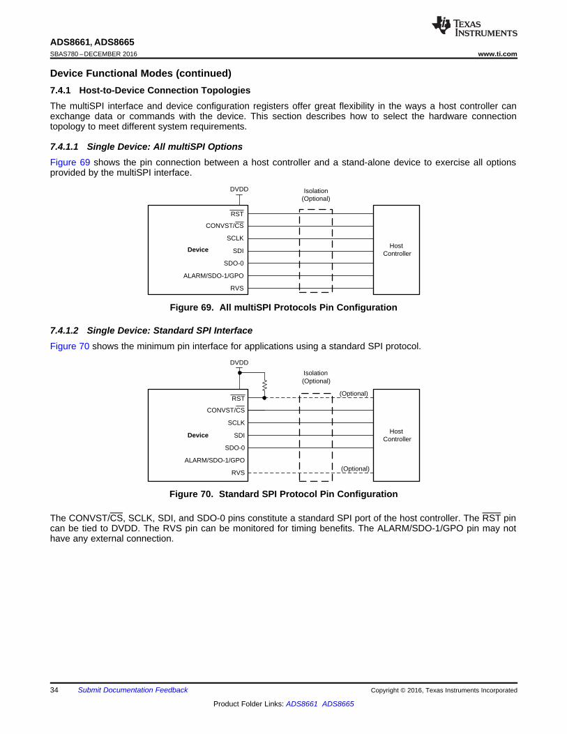
Device Functional Modes (continued)7.4.1 Host-to-Device Connection TopologiesThe multiSPI interface and device configuration registers offer great flexibility in the ways a host controller canexchange data or commands with the device. This section describes how to select the hardware connectiontopology to meet different system requirements.
7.4.1.1 Single Device: All multiSPI OptionsFigure 69 shows the pin connection between a host controller and a stand-alone device to exercise all optionsprovided by the multiSPI interface.
Figure 69. All multiSPI Protocols Pin Configuration
7.4.1.2 Single Device: Standard SPI InterfaceFigure 70 shows the minimum pin interface for applications using a standard SPI protocol.
Figure 70. Standard SPI Protocol Pin Configuration
The CONVST/CS, SCLK, SDI, and SDO-0 pins constitute a standard SPI port of the host controller. The RST pincan be tied to DVDD. The RVS pin can be monitored for timing benefits. The ALARM/SDO-1/GPO pin may nothave any external connection.

Device 1
SC
LK SD
I
SD
O-0
Device 2
RV
S
Device N
SC
LK SD
I
SD
O-0
RV
S
SC
LK SD
I
SD
O-0
RV
S
Isol
atio
n
(Opt
iona
l)
Host Controller
CO
NV
ST
/CS
SC
LK
SD
O
SD
I
CO
NV
ST
/CS
CO
NV
ST
/CS
CO
NV
ST
/CS
35
ADS8661, ADS8665www.ti.com SBAS780 –DECEMBER 2016
Product Folder Links: ADS8661 ADS8665
Submit Documentation FeedbackCopyright © 2016, Texas Instruments Incorporated
Device Functional Modes (continued)7.4.1.3 Multiple Devices: Daisy-Chain TopologyA typical connection diagram showing multiple devices in a daisy-chain topology is shown in Figure 71.
Figure 71. Daisy-Chain Connection Schematic
The CONVST/CS and SCLK inputs of all devices are connected together and controlled by a single CONVST/CSand SCLK pin of the host controller, respectively. The SDI input pin of the first device in the chain (device 1) isconnected to the SDO-x pin of the host controller, the SDO-0 output pin of device 1 is connected to the SDI inputpin of device 2, and so forth. The SDO-0 output pin of the last device in the chain (device N) is connected to theSDI pin of the host controller.
To operate multiple devices in a daisy-chain topology, the host controller must program the configurationregisters in each device with identical values. The devices must operate with a single SDO-0 output, using theexternal clock with any of the legacy, SPI-compatible protocols for data read and data write operations. In theSDO_CTL_REG register, bits 7-0 must be programmed to 00h.
All devices in the daisy-chain topology sample their analog input signals on the rising edge of the CONVST/CSsignal and the data transfer frame starts with a falling edge of the same signal. At the launch edge of the SCLKsignal, every device in the chain shifts out the MSB to the SDO-0 pin. On every SCLK capture edge, each devicein the chain shifts in data received on its SDI pin as the LSB bit of the unified shift register; see Figure 68.Therefore, in a daisy-chain configuration, the host controller receives the data of device N, followed by the dataof device N-1, and so forth (in MSB-first fashion). On the rising edge of the CONVST/CS signal, each devicedecodes the contents in its unified and takes appropriate action.
For N devices connected in a daisy-chain topology, an optimal data transfer frame must contain 32 × N SCLKcapture edges (see Figure 72). A shorter data transfer frame can result in an erroneous device configuration andmust be avoided. For a data transfer frame with > 32 × N SCLK capture edges, the host controller mustappropriately align the configuration data for each device before bringing CONVST/CS high.
Note that the overall throughput of the system is proportionally reduced with the number of devices connected ina daisy-chain topology.
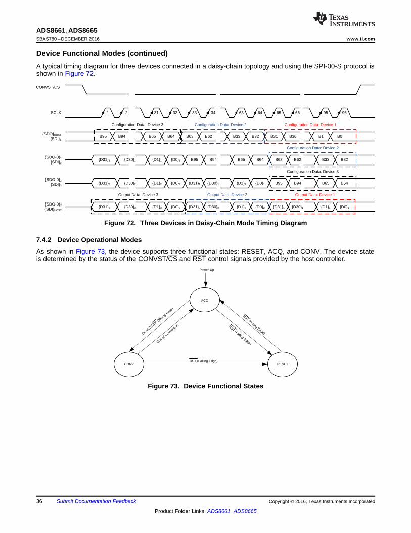
ACQ
CONV RESET
Power-Up
CONVST/CS (R
ising E
dge)
End of Conve
rsion
RST (Rising Edge)
RST (Falling Edge)
RST (Falling Edge)
Configuration Data: Device 3 Configuration Data: Device 2
SCLK
{SDO-0}1
{SDI}2{D31}1
CONVST/CS
{SDO}HOST
{SDI}1B64B65B95 B94 B63 B62
{D1}1 B95 B94
B32B33 B31 B30
B65 B64 B63 B62
B0B1
B33 B32{D30}1 {D0}1
{SDO-0}2
{SDI}3{D31}2 {D1}2 B95 B94 B65 B64{D30}2 {D0}2 {D31}1 {D30}1 {D1}1 {D0}1
{SDO-0}3
{SDI}HOST{D31}3 {D1}3{D30}3 {D0}3 {D31}2 {D30}2 {D1}2 {D0}2 {D31}1 {D30}1 {D1}1 {D0}1
1 2 31 32 33 34 63 64 65 66 95 96
Configuration Data: Device 1
Configuration Data: Device 2
Configuration Data: Device 3
Output Data: Device 3 Output Data: Device 2 Output Data: Device 1
36
ADS8661, ADS8665SBAS780 –DECEMBER 2016 www.ti.com
Product Folder Links: ADS8661 ADS8665
Submit Documentation Feedback Copyright © 2016, Texas Instruments Incorporated
Device Functional Modes (continued)A typical timing diagram for three devices connected in a daisy-chain topology and using the SPI-00-S protocol isshown in Figure 72.
Figure 72. Three Devices in Daisy-Chain Mode Timing Diagram
7.4.2 Device Operational ModesAs shown in Figure 73, the device supports three functional states: RESET, ACQ, and CONV. The device stateis determined by the status of the CONVST/CS and RST control signals provided by the host controller.
Figure 73. Device Functional States
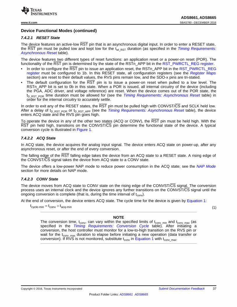
cycle-min conv acq-mint t t �
37
ADS8661, ADS8665www.ti.com SBAS780 –DECEMBER 2016
Product Folder Links: ADS8661 ADS8665
Submit Documentation FeedbackCopyright © 2016, Texas Instruments Incorporated
Device Functional Modes (continued)7.4.2.1 RESET StateThe device features an active-low RST pin that is an asynchronous digital input. In order to enter a RESET state,the RST pin must be pulled low and kept low for the twl_RST duration (as specified in the Timing Requirements:Asynchronous Reset table).
The device features two different types of reset functions: an application reset or a power-on reset (POR). Thefunctionality of the RST pin is determined by the state of the RSTn_APP bit in the RST_PWRCTL_REG register.• In order to configure the RST pin to issue an application reset, the RSTn_APP bit in the RST_PWRCTL_REG
register must be configured to 1b. In this RESET state, all configuration registers (see the Register Mapssection) are reset to their default values, the RVS pins remain low, and the SDO-x pins are tri-stated.
• The default configuration for the RST pin is to issue a power-on reset when pulled to a low level. TheRSTn_APP bit is set to 0b in this state. When a POR is issued, all internal circuitry of the device (includingthe PGA, ADC driver, and voltage reference) are reset. When the device comes out of the POR state, thetD_RST_POR time duration must be allowed for (see the Timing Requirements: Asynchronous Reset table) inorder for the internal circuitry to accurately settle.
In order to exit any of the RESET states, the RST pin must be pulled high with CONVST/CS and SCLK held low.After a delay of tD_RST_POR or tD_RST_APP (see the Timing Requirements: Asynchronous Reset table), the deviceenters ACQ state and the RVS pin goes high.
To operate the device in any of the other two states (ACQ or CONV), the RST pin must be held high. With theRST pin held high, transitions on the CONVST/CS pin determine the functional state of the device. A typicalconversion cycle is illustrated in Figure 1.
7.4.2.2 ACQ StateIn ACQ state, the device acquires the analog input signal. The device enters ACQ state on power-up, after anyasynchronous reset, or after the end of every conversion.
The falling edge of the RST falling edge takes the device from an ACQ state to a RESET state. A rising edge ofthe CONVST/CS signal takes the device from ACQ state to a CONV state.
The device offers a low-power NAP mode to reduce power consumption in the ACQ state; see the NAP Modesection for more details on NAP mode.
7.4.2.3 CONV StateThe device moves from ACQ state to CONV state on the rising edge of the CONVST/CS signal. The conversionprocess uses an internal clock and the device ignores any further transitions on the CONVST/CS signal until theongoing conversion is complete (that is, during the time interval of tconv).
At the end of conversion, the device enters ACQ state. The cycle time for the device is given by Equation 1:
(1)
NOTEThe conversion time, tconv, can vary within the specified limits of tconv_min and tconv_max (asspecified in the Timing Requirements: Conversion Cycle table). After initiating aconversion, the host controller must monitor for a low-to-high transition on the RVS pin orwait for the tconv_max duration to elapse before initiating a new operation (data transfer orconversion). If RVS is not monitored, substitute tconv in Equation 1 with tconv_max.
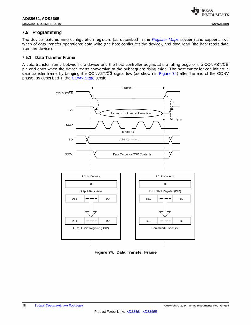
Frame F
RVS
CONVST/CS
td_RVS
SCLK
SDI Valid Command
As per output protocol selection.
N SCLKs
SDO-x
Output Data Word
Output Shift Register (OSR)
D0
D31 D0
D31
0
SCLK Counter
N
SCLK Counter
Input Shift Register (ISR)
Command Processor
B0
B31 B0
B31
Data Output or OSR Contents
38
ADS8661, ADS8665SBAS780 –DECEMBER 2016 www.ti.com
Product Folder Links: ADS8661 ADS8665
Submit Documentation Feedback Copyright © 2016, Texas Instruments Incorporated
7.5 ProgrammingThe device features nine configuration registers (as described in the Register Maps section) and supports twotypes of data transfer operations: data write (the host configures the device), and data read (the host reads datafrom the device).
7.5.1 Data Transfer FrameA data transfer frame between the device and the host controller begins at the falling edge of the CONVST/CSpin and ends when the device starts conversion at the subsequent rising edge. The host controller can initiate adata transfer frame by bringing the CONVST/CS signal low (as shown in Figure 74) after the end of the CONVphase, as described in the CONV State section.
Figure 74. Data Transfer Frame
39
ADS8661, ADS8665www.ti.com SBAS780 –DECEMBER 2016
Product Folder Links: ADS8661 ADS8665
Submit Documentation FeedbackCopyright © 2016, Texas Instruments Incorporated
Programming (continued)For a typical data transfer frame F:1. The host controller pulls CONVST/CS low to initiate a data transfer frame. On the falling edge of the
CONVST/CS signal:– RVS goes low, indicating the beginning of the data transfer frame.– The internal SCLK counter is reset to 0.– The device takes control of the data bus. As illustrated in Figure 74, the contents of the output data word
are loaded into the 32-bit output shift register (OSR).– The internal configuration register is reset to 0000h, corresponding to a NOP command.
2. During the frame, the host controller provides clocks on the SCLK pin:– On each SCLK capture edge, the SCLK counter is incremented and the data bit received on the SDI pin
is shifted into the LSB of the input shift register.– On each launch edge of the output clock (SCLK in this case), the MSB of the output shift register data is
shifted out on the selected SDO-x pins.– The status of the RVS pin depends on the output protocol selection (see the Protocols for Reading From
the Device section).3. The host controller pulls the CONVST/CS pin high to end the data transfer frame. On the rising edge of
CONVST/CS:– The SDO-x pins go to tri-state.– As illustrated in Figure 74, the contents of the input shift register are transferred to the command
processor for decoding and further action.– RVS output goes low, indicating the beginning of conversion.
After pulling CONVST/CS high, the host controller must monitor for a low-to-high transition on the RVS pin orwait for the tconv_max time (see the Timing Requirements: Conversion Cycle table) to elapse before initiating a newdata transfer frame.
At the end of the data transfer frame F:• If the SCLK counter = 32, then the device treats the frame F as an optimal data transfer frame for any read or
write operation. At the end of an optimal data transfer frame, the command processor treats the 32-bitcontents of the input shift register as a valid command word.
• If the SCLK counter is < 32, then the device treats the frame F as a short data transfer frame.– The data write operation to the device in invalid and the device treats this frame as an NOP command.– The output data bits transferred during a short frame on the SDO-x pins are still valid data. The host
controller can use the short data transfer frame to read only the required number of MSB bits from the 32-bit output shift register.
• If the SCLK counter is > 32, then the device treats the frame F as a long data transfer frame. At the end of along data transfer frame, the command processor treats the 32-bit contents of the input shift register as avalid command word. There is no restriction on the maximum number of clocks that can be provided withinany data transfer frame F. However, when the host controller provides a long data transfer frame, the last 32bits shifted into the device prior to the CONVST/CS rising edge must constitute the desired command.
40
ADS8661, ADS8665SBAS780 –DECEMBER 2016 www.ti.com
Product Folder Links: ADS8661 ADS8665
Submit Documentation Feedback Copyright © 2016, Texas Instruments Incorporated
Programming (continued)7.5.2 Input Command Word and Register Write OperationAny data write operation to the device is always synchronous to the external clock provided on the SCLK pin.
The device allows either one byte or two bytes (equivalent to half a word) to be read or written during any deviceprogramming operation. Table 5 lists the input commands supported by the device. The input commandsassociated with reading or writing two bytes in a single operation are suffixed as HWORD.
For any HWORD command, the LSB of the 9-bit address is always ignored and considered as 0b. For example,regardless whether address 04h or 05h is entered for any particular HWORD command, the device alwaysexercises the command on address 04h.
Table 5. List of Input CommandsOPCODEB[31:0]
COMMANDACRONYM COMMAND DESCRIPTION
00000000_000000000_00000000_00000000 NOP No operation
11000_xx_<9-bit address>_<16-bit data> CLEAR_HWORD
• Command used to clear any (or a group of) bits of a register.• Any bit marked 1 in the data field results in that particular bit of the specified register being
reset to 0, leaving the other bits unchanged.• Half-word command (that is, the command functions on 16 bits at a time).• LSB of the 9-bit address is always ignored and considered as 0b.
11001_xx_<9-bit address>_00000000_00000000 READ_HWORD
• Command used to perform a 16-bit read operation.• Half-word command (that is, the device outputs 16 bits of register data at a time).• LSB of the 9-bit address is always ignored and considered as 0b.• Upon receiving this command, the device sends out 16 bits of the register in the next frame.
01001_xx_<9-bit address>_00000000_00000000 READ • Same as the READ_HWORD except that only eight bits of the register (byte read) are
returned in the next frame.
11010_00_<9-bit address>_<16-bit data>
WRITE
• Half-word write command (two bytes of input data are written into the specified address).• LSB of the 9-bit address is always ignored and considered as 0b.
11010_01_<9-bit address>_<16-bit data>
• Half-word write command.• LSB of the 9-bit address is always ignored and considered as 0b.• With this command, only the MS byte of the 16-bit data word is written at the specified
register address. The LS byte is ignored.
11010_10_<9-bit address>_<16-bit data>
• Half-word write command.• LSB of the 9-bit address is always ignored and considered as 0b.• With this command, only the LS byte of the 16-bit data word is written at the specified register
address. The MS byte is ignored.
11011_xx_<9-bit address>_<16-bit data> SET_HWORD
• Command used to set any (or a group of) bits of a register.• Any bit marked 1 in the data field results in that particular bit of the specified register being set
to 1, leaving the other bits unchanged.• Half-word command (that is, the command functions on 16 bits at a time).• LSB of the 9-bit address is always ignored and considered as 0b.
All other input commandcombinations NOP No operation
All input commands (including the CLEAR_HWORD, WRITE, and SET_HWORD commands listed in Table 5)used to configure the internal registers must be 32 bits long. If any of these commands are provided in aparticular data frame F, that command gets executed at the rising edge of the CONVST/CS signal.

41
ADS8661, ADS8665www.ti.com SBAS780 –DECEMBER 2016
Product Folder Links: ADS8661 ADS8665
Submit Documentation FeedbackCopyright © 2016, Texas Instruments Incorporated
7.5.3 Output Data WordThe data read from the device can be synchronized to the external clock on the SCLK pin or to an internal clockof the device by programming the configuration registers (see the Data Transfer Protocols section for details).
In any data transfer frame, the contents of the internal output shift register are shifted out on the SDO-x pins. Theoutput data for any frame (F+1) is determined by the command issued in frame F and the status ofDATA_VAL[2:0] bits:• If DATA_VAL[2:0] bits in DATAOUT_CTL_REG register are set to 1xxb, then the output data word for frame
(F+1) contains fixed data pattern as described in the DATAOUT_CTL_REG register.• If a valid READ command is issued in frame F, the output data word for frame (F+1) contains 8-bit register
data, followed by 0's.• If a valid READ_HWORD command is issued in frame F, the output data word for frame (F+1) contains 16-bit
register data, followed by 0's.• For all other combinations, the output data word for frame (F+1) contains the latest 12-bit conversion result.
Program the DATAOUT_CTL_REG register to append various data flags to the conversion result. The dataflags are appended as per following sequence:1. DEVICE_ADDR[3:0] bits are appended if the DEVICE_ADDR_INCL bit is set to 12. AVDD ALARM FLAGS are appended if the VDD_ACTIVE_ALARM_INCL bit is set to 13. INPUT ALARM FLAGS are appended if the IN_ACTIVE_ALARM_INCL bit is set to 14. ADC INPUT RANGE FLAGS are appended if the RANGE_INCL bit is set to 15. PARITY bits are appended if the PAR_EN bit is set to 16. All the remaining bits in the 32-bit output data word are set to 0.
Table 6 shows the output data word with all data flags enabled.
Table 6. Output Data Word With All Data Flags EnabledDEVICE_ADDR_INCL = 1b, VDD_ACTIVE_ALARM_INCL = 1b, IN_ACTIVE_ALARM_INCL = 1b, RANGE_INCL = 1b, and PAR_EN = 1b
D[31:20] D[19:16] D[15:14] D[13:12] D[11:8] D[7:6] D[5:0]
Conversion result Device address AVDD alarm flags Input alarm flags ADC input range Parity bits 000000b
Table 7 shows output data word with only some of the data flags enabled.
Table 7. Output Data Word With Only Some Data Flags EnabledDEVICE_ADDR_INCL = 0b, VDD_ACTIVE_ALARM_INCL = 1b, IN_ACTIVE_ALARM_INCL = 0b, RANGE_INCL = 1b, and PAR_EN = 1b
D[31:20] D[19:18] D[17:14] D[13:12] D[11:0]
Conversion result AVDD alarm flags ADC input range Parity bits 000000000000b
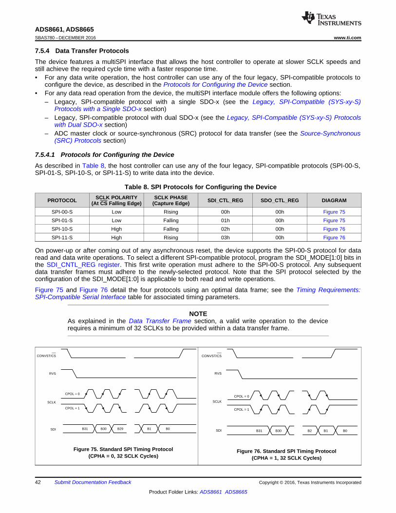
SCLK
SDI
RVS
CPOL = 0
CPOL = 1
CONVST/CS
B31 B30 B2 B1 B0
SCLK
SDI
RVS
CPOL = 0
CPOL = 1
CONVST/CS
B31 B30 B29 B1 B0
42
ADS8661, ADS8665SBAS780 –DECEMBER 2016 www.ti.com
Product Folder Links: ADS8661 ADS8665
Submit Documentation Feedback Copyright © 2016, Texas Instruments Incorporated
7.5.4 Data Transfer ProtocolsThe device features a multiSPI interface that allows the host controller to operate at slower SCLK speeds andstill achieve the required cycle time with a faster response time.• For any data write operation, the host controller can use any of the four legacy, SPI-compatible protocols to
configure the device, as described in the Protocols for Configuring the Device section.• For any data read operation from the device, the multiSPI interface module offers the following options:
– Legacy, SPI-compatible protocol with a single SDO-x (see the Legacy, SPI-Compatible (SYS-xy-S)Protocols with a Single SDO-x section)
– Legacy, SPI-compatible protocol with dual SDO-x (see the Legacy, SPI-Compatible (SYS-xy-S) Protocolswith Dual SDO-x section)
– ADC master clock or source-synchronous (SRC) protocol for data transfer (see the Source-Synchronous(SRC) Protocols section)
7.5.4.1 Protocols for Configuring the DeviceAs described in Table 8, the host controller can use any of the four legacy, SPI-compatible protocols (SPI-00-S,SPI-01-S, SPI-10-S, or SPI-11-S) to write data into the device.
Table 8. SPI Protocols for Configuring the Device
PROTOCOL SCLK POLARITY(At CS Falling Edge)
SCLK PHASE(Capture Edge) SDI_CTL_REG SDO_CTL_REG DIAGRAM
SPI-00-S Low Rising 00h 00h Figure 75SPI-01-S Low Falling 01h 00h Figure 75SPI-10-S High Falling 02h 00h Figure 76SPI-11-S High Rising 03h 00h Figure 76
On power-up or after coming out of any asynchronous reset, the device supports the SPI-00-S protocol for dataread and data write operations. To select a different SPI-compatible protocol, program the SDI_MODE[1:0] bits inthe SDI_CNTL_REG register. This first write operation must adhere to the SPI-00-S protocol. Any subsequentdata transfer frames must adhere to the newly-selected protocol. Note that the SPI protocol selected by theconfiguration of the SDI_MODE[1:0] is applicable to both read and write operations.
Figure 75 and Figure 76 detail the four protocols using an optimal data frame; see the Timing Requirements:SPI-Compatible Serial Interface table for associated timing parameters.
NOTEAs explained in the Data Transfer Frame section, a valid write operation to the devicerequires a minimum of 32 SCLKs to be provided within a data transfer frame.
Figure 75. Standard SPI Timing Protocol(CPHA = 0, 32 SCLK Cycles)
Figure 76. Standard SPI Timing Protocol(CPHA = 1, 32 SCLK Cycles)
43
ADS8661, ADS8665www.ti.com SBAS780 –DECEMBER 2016
Product Folder Links: ADS8661 ADS8665
Submit Documentation FeedbackCopyright © 2016, Texas Instruments Incorporated
7.5.4.2 Protocols for Reading From the DeviceThe protocols for the data read operation can be broadly classified into three categories:1. Legacy, SPI-compatible protocols with a single SDO-x2. Legacy, SPI-compatible protocols with dual SDO-x3. ADC master clock or source-synchronous (SRC) protocol for data transfer
7.5.4.2.1 Legacy, SPI-Compatible (SYS-xy-S) Protocols with a Single SDO-x
As shown in Table 9, the host controller can use any of the four legacy, SPI-compatible protocols (SPI-00-S, SPI-01-S, SPI-10-S, or SPI-11-S) to read data from the device.
Table 9. SPI Protocols for Reading From the Device
PROTOCOLSCLK POLARITY
(At CS FallingEdge)
SCLK PHASE(Capture Edge)
MSB BITLAUNCH EDGE SDI_CTL_REG SDO_CTL_REG DIAGRAM
SPI-00-S Low Rising CS falling 00h 00h Figure 77SPI-01-S Low Falling 1st SCLK rising 01h 00h Figure 77SPI-10-S High Falling CS falling 02h 00h Figure 78SPI-11-S High Rising 1st SCLK falling 03h 00h Figure 78
On power-up or after coming out of any asynchronous reset, the device supports the SPI-00-S protocol for dataread and data write operations. To select a different SPI-compatible protocol for both the data transferoperations:1. Program the SDI_MODE[1:0] bits in the SDI_CTL_REG register. This first write operation must adhere to the
SPI-00-S protocol. Any subsequent data transfer frames must adhere to the newly-selected protocol.2. Set the SDO_MODE[1:0] bits = 00b in the SDO_CTL_REG register.
NOTEThe SPI transfer protocol selected by configuring the SDI_MODE[1:0] bits in theSDI_CTL_REG register determines the data transfer protocol for both write and readoperations. Either data can be read from the device using the selected SPI protocol byconfiguring the SDO_MODE[1:0] bits = 00b in the SDO_CTL_REG register, or one of theSRC protocols can be selected for data read, as explained in the Source-Synchronous(SRC) Protocols section.
When using any of the SPI-compatible protocols, the RVS output remains low throughout the data transfer frame;see the Timing Requirements: SPI-Compatible Serial Interface table for associated timing parameters.
Figure 77 and Figure 78 explain the details of the four protocols. As explained in the Data Transfer Framesection, the host controller can use a short data transfer frame to read only the required number of MSB bitsfrom the 32-bit output data word.
If the host controller uses a long data transfer frame with SDO_CNTL_REG[7:0] = 00h, then the device exhibitsdaisy-chain operation (see the Multiple Devices: Daisy-Chain Topology section).

SCLK
SDO-0 0 M M-2 L+3 L+1
RVS
CPOL = 0
CPOL = 1
CONVST/CS
0 M-1 M-1 L+2 LSDO-1
SCLK
SDO-0 M M-2 M-4 L+3 L+1
RVS
CPOL = 0
CPOL = 1
CONVST/CS
SDO-1 M-1 M-3 M-5 L+2 L
SCLK
SDO-00 M M-1 L+1 L
RVS
CPOL = 0
CPOL = 1
CONVST/CS
SCLK
SDO-0 M M-1 M-2 L+1 L
RVS
CPOL = 0
CPOL = 1
CONVST/CS
44
ADS8661, ADS8665SBAS780 –DECEMBER 2016 www.ti.com
Product Folder Links: ADS8661 ADS8665
Submit Documentation Feedback Copyright © 2016, Texas Instruments Incorporated
Figure 77. Standard SPI Timing Protocol(CPHA = 0, Single SDO-x)
Figure 78. Standard SPI Timing Protocol(CPHA = 1, Single SDO-x)
7.5.4.2.2 Legacy, SPI-Compatible (SYS-xy-S) Protocols with Dual SDO-x
The device provides an option to increase the SDO-x bus width from one bit (default, single SDO-x) to two bits(dual SDO-x) when operating with any of the data transfer protocols. In order to operate the device in dual SDOmode, the SDO1_CONFIG[1:0] bits in the SDO_CTL_REG register must be set to 11b. In this mode, theALARM/SDO-1/GPO pin functions as SDO-1.
In dual SDO mode, two bits of data are launched on the two SDO-x pins (SDO-0 and SDO-1) on every SCLKlaunch edge, as shown in Figure 79 and Figure 80.
Figure 79. Standard SPI Timing Protocol(CPHA = 0, Dual SDO-x) Figure 80. Standard SPI Timing Protocol
(CPHA = 1, Dual SDO-x)
NOTEFor any particular SPI protocol, the device follows the same timing specifications for singleand dual SDO modes. The only difference is that the device requires half as many SCLKcycles to output the same number of bits when in single SDO mode, thus reducing theminimum required SCLK frequency for a certain sampling rate of the ADC.
45
ADS8661, ADS8665www.ti.com SBAS780 –DECEMBER 2016
Product Folder Links: ADS8661 ADS8665
Submit Documentation FeedbackCopyright © 2016, Texas Instruments Incorporated
7.5.4.2.3 Source-Synchronous (SRC) Protocols
The multiSPI interface supports an ADC master clock or source-synchronous mode of data transfer between thedevice and host controller. In this mode, the device provides an output clock that is synchronous with the outputdata. Furthermore, the host controller can also select the output clock source and data bus width options in thismode of operation. In all SRC modes of operation, the RVS pin provides the output clock, synchronous to thedevice data output.
The SRC protocol allows the clock source (internal or external) and the width of the output bus to be configured,similar to the SPI protocols.
7.5.4.2.3.1 Output Clock Source Options
The device allows the output clock on the RVS pin to be synchronous to either the external clock provided on theSCLK pin or to the internal clock of the device. This selection is done by configuring the SSYNC_CLK bit, asexplained in the SDO_CTL_REG register. The timing diagram and specifications for operating the device with anSRC protocol in external CLK mode are provided in Figure 7 and the Timing Requirements: Source-SynchronousSerial Interface (External Clock) table. The timing diagram and specifications for operating the device with anSRC protocol in internal CLK mode are provided in Figure 8 and the Timing Requirements: Source-SynchronousSerial Interface (Internal Clock) table.
7.5.4.2.3.2 Output Bus Width Options
The device provides an option to increase the SDO-x bus width from one bit (default, single SDO-x) to two bits(dual SDO-x) when operating with any of the SRC protocols. In order to operate the device in dual SDO mode,the SDO1_CONFIG[1:0] bits in the SDO_CTL_REG register must be set to 11b. In this mode, the ALARM/SDO-1/GPO pin functions as SDO-1.
NOTEFor any particular SRC protocol, the device follows the same timing specifications forsingle and dual SDO modes. The only difference is that the device requires half as manyclock cycles to output the same number of bits when in single SDO mode, thus reducingthe minimum required clock frequency for a certain sampling rate of the ADC.
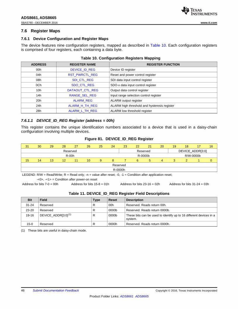
46
ADS8661, ADS8665SBAS780 –DECEMBER 2016 www.ti.com
Product Folder Links: ADS8661 ADS8665
Submit Documentation Feedback Copyright © 2016, Texas Instruments Incorporated
7.6 Register Maps
7.6.1 Device Configuration and Register MapsThe device features nine configuration registers, mapped as described in Table 10. Each configuration registersis comprised of four registers, each containing a data byte.
Table 10. Configuration Registers MappingADDRESS REGISTER NAME REGISTER FUNCTION
00h DEVICE_ID_REG Device ID register04h RST_PWRCTL_REG Reset and power control register08h SDI_CTL_REG SDI data input control register0Ch SDO_CTL_REG SDO-x data input control register10h DATAOUT_CTL_REG Output data control register14h RANGE_SEL_REG Input range selection control register20h ALARM_REG ALARM output register24h ALARM_H_TH_REG ALARM high threshold and hysteresis register28h ALARM_L_TH_REG ALARM low threshold register
7.6.1.1 DEVICE_ID_REG Register (address = 00h)This register contains the unique identification numbers associated to a device that is used in a daisy-chainconfiguration involving multiple devices.
Figure 81. DEVICE_ID_REG Register
31 30 29 28 27 26 25 24 23 22 21 20 19 18 17 16Reserved Reserved DEVICE_ADDR[3:0]
R-00h R-0000b R/W-0000b15 14 13 12 11 10 9 8 7 6 5 4 3 2 1 0
ReservedR-0000h
LEGEND: R/W = Read/Write; R = Read only; -n = value after reset; -0, -1 = Condition after application reset;LEGEND: -<0>, -<1> = Condition after power-on resetAddress for bits 7-0 = 00h Address for bits 15-8 = 01h Address for bits 23-16 = 02h Address for bits 31-24 = 03h
(1) These bits are useful in daisy-chain mode.
Table 11. DEVICE_ID_REG Register Field DescriptionsBit Field Type Reset Description
31-24 Reserved R 00h Reserved. Reads return 00h.23-20 Reserved R 0000b Reserved. Reads return 0000b.19-16 DEVICE_ADDR[3:0] (1) R 0000b These bits can be used to identify up to 16 different devices in a
system.15-0 Reserved R 0000h Reserved. Reads return 0000h.

47
ADS8661, ADS8665www.ti.com SBAS780 –DECEMBER 2016
Product Folder Links: ADS8661 ADS8665
Submit Documentation FeedbackCopyright © 2016, Texas Instruments Incorporated
7.6.1.2 RST_PWRCTL_REG Register (address = 04h)This register controls the reset and power-down features offered by the converter.
Any write operation to the RST_PWRCTL_REG register must be preceded by a write operation with the registeraddress set to 05h and the register data set to 69h.
Figure 82. RST_PWRCTL_REG Register
31 30 29 28 27 26 25 24 23 22 21 20 19 18 17 16ReservedR-0000h
15 14 13 12 11 10 9 8 7 6 5 4 3 2 1 0
WKEY[7:0] Reserved VDD_AL_DIS IN_AL_DIS Reserved RSTn_APP NAP_EN PWRDN
R/W-00h R-00b R/W-0b R/W-0b R-0b R/W-<0>b R/W-<0>b R/W-0bLEGEND: R/W = Read/Write; R = Read only; -n = value after reset; -0, -1 = Condition after application reset;LEGEND: -<0>, -<1> = Condition after power-on resetAddress for bits 7-0 = 04h Address for bits 15-8 = 05h Address for bits 23-16 = 06h Address for bits 31-24 = 07h
(1) Setting this bit forces the RST pin to function as an application reset until the next power cycle.(2) See the Electrical Characteristics table for details on the latency encountered when entering and exiting the associated low-power
mode.
Table 12. RST_PWRCTL_REG Register Field DescriptionsBit Field Type Reset Description
31-16 Reserved R 0000h Reserved. Reads return 0000h.15-8 WKEY[7:0] R/W 00h This value functions as a protection key to enable writes to bits 5-0.
Bits are written only if WKEY is set to 69h first.7-6 Reserved R 00b Reserved. Reads return 00b5 VDD_AL_DIS R/W 0b 0b = VDD alarm is enabled
1b = VDD alarm is disabled4 IN_AL_DIS R/W 0b 0b = Input alarm is enabled
1b = Input alarm is disabled3 Reserved R 0b Reserved. Reads return 0h.2 RSTn_APP (1) R/W 0b 0b = RST pin functions as a POR class reset (causes full device
initialization)1b = RST pin functions as an application reset (only user-programmedmodes are cleared)
1 NAP_EN (2) R/W 0b 0b = Disables the NAP mode of the converter1b = Enables the converter to enter NAP mode if CONVST/CS is heldhigh after the current conversion completes
0 PWRDN (2) R/W 0b 0b = Puts the converter into active mode1b = Puts the converter into power-down mode
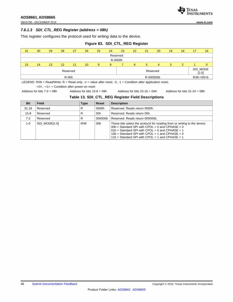
48
ADS8661, ADS8665SBAS780 –DECEMBER 2016 www.ti.com
Product Folder Links: ADS8661 ADS8665
Submit Documentation Feedback Copyright © 2016, Texas Instruments Incorporated
7.6.1.3 SDI_CTL_REG Register (address = 08h)This register configures the protocol used for writing data to the device.
Figure 83. SDI_CTL_REG Register
31 30 29 28 27 26 25 24 23 22 21 20 19 18 17 16ReservedR-0000h
15 14 13 12 11 10 9 8 7 6 5 4 3 2 1 0
Reserved Reserved SDI_MODE[1:0]
R-00h R-000000b R/W-<00>bLEGEND: R/W = Read/Write; R = Read only; -n = value after reset; -0, -1 = Condition after application reset;LEGEND: -<0>, -<1> = Condition after power-on resetAddress for bits 7-0 = 08h Address for bits 15-8 = 09h Address for bits 23-16 = 0Ah Address for bits 31-24 = 0Bh
Table 13. SDI_CTL_REG Register Field DescriptionsBit Field Type Reset Description
31-16 Reserved R 0000h Reserved. Reads return 0000h.15-8 Reserved R 00h Reserved. Reads return 00h.7-2 Reserved R 000000b Reserved. Reads return 000000b.1-0 SDI_MODE[1:0] R/W 00b These bits select the protocol for reading from or writing to the device.
00b = Standard SPI with CPOL = 0 and CPHASE = 001b = Standard SPI with CPOL = 0 and CPHASE = 110b = Standard SPI with CPOL = 1 and CPHASE = 011b = Standard SPI with CPOL = 1 and CPHASE = 1
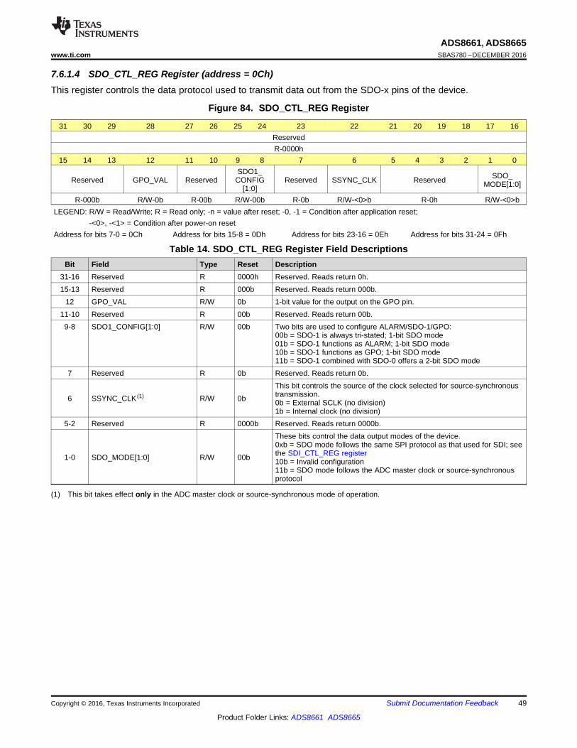
49
ADS8661, ADS8665www.ti.com SBAS780 –DECEMBER 2016
Product Folder Links: ADS8661 ADS8665
Submit Documentation FeedbackCopyright © 2016, Texas Instruments Incorporated
7.6.1.4 SDO_CTL_REG Register (address = 0Ch)This register controls the data protocol used to transmit data out from the SDO-x pins of the device.
Figure 84. SDO_CTL_REG Register
31 30 29 28 27 26 25 24 23 22 21 20 19 18 17 16ReservedR-0000h
15 14 13 12 11 10 9 8 7 6 5 4 3 2 1 0
Reserved GPO_VAL ReservedSDO1_
CONFIG[1:0]
Reserved SSYNC_CLK Reserved SDO_MODE[1:0]
R-000b R/W-0b R-00b R/W-00b R-0b R/W-<0>b R-0h R/W-<0>bLEGEND: R/W = Read/Write; R = Read only; -n = value after reset; -0, -1 = Condition after application reset;LEGEND: -<0>, -<1> = Condition after power-on resetAddress for bits 7-0 = 0Ch Address for bits 15-8 = 0Dh Address for bits 23-16 = 0Eh Address for bits 31-24 = 0Fh
(1) This bit takes effect only in the ADC master clock or source-synchronous mode of operation.
Table 14. SDO_CTL_REG Register Field DescriptionsBit Field Type Reset Description
31-16 Reserved R 0000h Reserved. Reads return 0h.15-13 Reserved R 000b Reserved. Reads return 000b.
12 GPO_VAL R/W 0b 1-bit value for the output on the GPO pin.11-10 Reserved R 00b Reserved. Reads return 00b.9-8 SDO1_CONFIG[1:0] R/W 00b Two bits are used to configure ALARM/SDO-1/GPO:
00b = SDO-1 is always tri-stated; 1-bit SDO mode01b = SDO-1 functions as ALARM; 1-bit SDO mode10b = SDO-1 functions as GPO; 1-bit SDO mode11b = SDO-1 combined with SDO-0 offers a 2-bit SDO mode
7 Reserved R 0b Reserved. Reads return 0b.
6 SSYNC_CLK (1) R/W 0b
This bit controls the source of the clock selected for source-synchronoustransmission.0b = External SCLK (no division)1b = Internal clock (no division)
5-2 Reserved R 0000b Reserved. Reads return 0000b.
1-0 SDO_MODE[1:0] R/W 00b
These bits control the data output modes of the device.0xb = SDO mode follows the same SPI protocol as that used for SDI; seethe SDI_CTL_REG register10b = Invalid configuration11b = SDO mode follows the ADC master clock or source-synchronousprotocol

50
ADS8661, ADS8665SBAS780 –DECEMBER 2016 www.ti.com
Product Folder Links: ADS8661 ADS8665
Submit Documentation Feedback Copyright © 2016, Texas Instruments Incorporated
7.6.1.5 DATAOUT_CTL_REG Register (address = 10h)This register controls the data output by the device.
Figure 85. DATAOUT_CTL_REG Register
31 30 29 28 27 26 25 24 23 22 21 20 19 18 17 16ReservedR-0000h
15 14 13 12 11 10 9 8 7 6 5 4 3 2 1 0
ReservedDEVICE_ADDR_INCL
VDD_ACTIVE_ALARM_INCL[1:0]
IN_ACTIVE_ALARM_INCL[1:0] Reserved RANGE_
INCL Reserved PAR_EN DATA_VAL[2:0]
R-0b R/W-0b R/W-0b R/W-0b R-0b R/W-0b R-0000b R/W-<0>b
R/W-000b
LEGEND: R/W = Read/Write; R = Read only; -n = value after reset; -0, -1 = Condition after application reset;LEGEND: -<0>, -<1> = Condition after power-on resetAddress for bits 7-0 = 10h Address for bits 15-8 = 11h Address for bits 23-16 = 12h Address for bits 31-24 = 13h
(1) Setting this bit increases the length of the output data by two bits.
Table 15. DATAOUT_CTL_REG Register Field DescriptionsBit Field Type Reset Description
31-16 Reserved R 0000h Reserved. Reads return 0000h.15 Reserved R 0b Reserved. Reads return 0b.14 DEVICE_ADDR_INCL R/W 0b Control to include the 4-bit DEVICE_ADDR register value in the
SDO-x output bit stream.0b = Do not include the register value1b = Include the register value
13-12 VDD_ACTIVE_ALARM_INCL[1:0] R/W 00b Control to include the active VDD ALARM flags in the SDO-x outputbit stream.00b = Do not include01b = Include ACTIVE_VDD_H_FLAG10b = Include ACTIVE_VDD_L_FLAG11b = Include both flags
11-10 IN_ACTIVE_ALARM_INCL[1:0] R/W 00b Control to include the active input ALARM flags in the SDO-x outputbit stream.00b = Do not include01b = Include ACTIVE_IN_H_FLAG10b = Include ACTIVE_IN_L_FLAG11b = Include both flags
9 Reserved R 0b Reserved. Reads return 0h.8 RANGE_INCL R/W 0b Control to include the 4-bit input range setting in the SDO-x output
bit stream.0b = Do not include the range configuration register value1b = Include the range configuration register value
7-4 Reserved R 0000b Reserved. Reads return 0000b.
3 PAR_EN (1) R/W 0b
0b = Output data does not contain parity information1b = Two parity bits (ADC output and output data frame) areappended to the LSBs of the output dataThe ADC output parity bit reflects an even parity for the ADC outputbits only.The output data frame parity bit reflects an even parity signature forthe entire output data frame, including the ADC output bits and anyinternal flags or register settings.
2-0 DATA_VAL[2:0] R/W 000b These bits control the data value output by the converter.0xxb = Value output is the conversion data100b = Value output is all 0's101b = Value output is all 1's110b = Value output is alternating 0's and 1's111b = Value output is alternating 00's and 11's
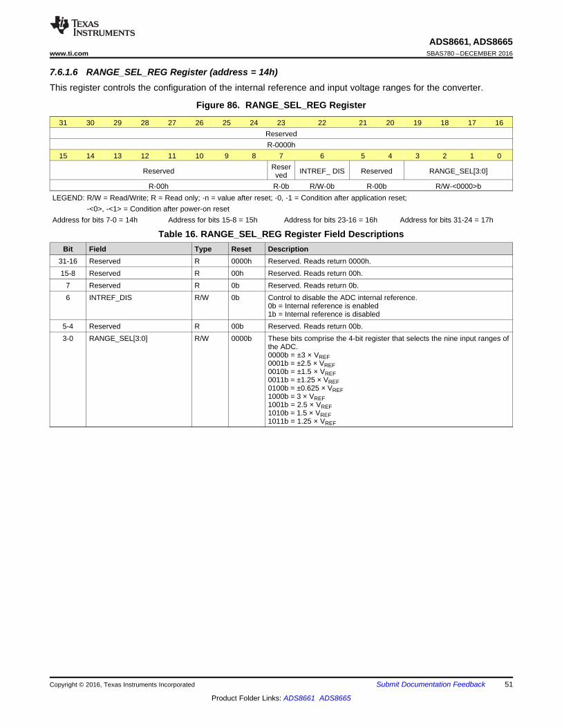
51
ADS8661, ADS8665www.ti.com SBAS780 –DECEMBER 2016
Product Folder Links: ADS8661 ADS8665
Submit Documentation FeedbackCopyright © 2016, Texas Instruments Incorporated
7.6.1.6 RANGE_SEL_REG Register (address = 14h)This register controls the configuration of the internal reference and input voltage ranges for the converter.
Figure 86. RANGE_SEL_REG Register
31 30 29 28 27 26 25 24 23 22 21 20 19 18 17 16ReservedR-0000h
15 14 13 12 11 10 9 8 7 6 5 4 3 2 1 0
Reserved Reserved INTREF_ DIS Reserved RANGE_SEL[3:0]
R-00h R-0b R/W-0b R-00b R/W-<0000>bLEGEND: R/W = Read/Write; R = Read only; -n = value after reset; -0, -1 = Condition after application reset;LEGEND: -<0>, -<1> = Condition after power-on resetAddress for bits 7-0 = 14h Address for bits 15-8 = 15h Address for bits 23-16 = 16h Address for bits 31-24 = 17h
Table 16. RANGE_SEL_REG Register Field DescriptionsBit Field Type Reset Description
31-16 Reserved R 0000h Reserved. Reads return 0000h.15-8 Reserved R 00h Reserved. Reads return 00h.
7 Reserved R 0b Reserved. Reads return 0b.6 INTREF_DIS R/W 0b Control to disable the ADC internal reference.
0b = Internal reference is enabled1b = Internal reference is disabled
5-4 Reserved R 00b Reserved. Reads return 00b.3-0 RANGE_SEL[3:0] R/W 0000b These bits comprise the 4-bit register that selects the nine input ranges of
the ADC.0000b = ±3 × VREF0001b = ±2.5 × VREF0010b = ±1.5 × VREF0011b = ±1.25 × VREF0100b = ±0.625 × VREF1000b = 3 × VREF1001b = 2.5 × VREF1010b = 1.5 × VREF1011b = 1.25 × VREF

52
ADS8661, ADS8665SBAS780 –DECEMBER 2016 www.ti.com
Product Folder Links: ADS8661 ADS8665
Submit Documentation Feedback Copyright © 2016, Texas Instruments Incorporated
7.6.1.7 ALARM_REG Register (address = 20h)This register contains the output alarm flags (active and tripped) for the input and AVDD alarm.
Figure 87. ALARM_REG Register
31 30 29 28 27 26 25 24 23 22 21 20 19 18 17 16ReservedR-0000h
15 14 13 12 11 10 9 8 7 6 5 4 3 2 1 0ACTIVE_VDD_L_
FLAG
ACTIVE_VDD_H_
FLAGReserved
ACTIVE_IN_L_FLAG
ACTIVE_IN_H_FLAG
ReservedTRP_
VDD_L_FLAG
TRP_VDD_H_
FLAG
TRP_IN_L_FLAG
TRP_IN_H_FLAG Reserved OVW_
ALARM
R-0b R-0b R-00b R-0b R-0b R-00b R-0b R-0b R-0b R-0b R-000b R-0bLEGEND: R = Read only; -n = value after reset; -0, -1 = Condition after application reset; -<0>, -<1> = Condition after power-on resetAddress for bits 7-0 = 20h Address for bits 15-8 = 21h Address for bits 23-16 = 22h Address for bits 31-24 = 23h
Table 17. ALARM_REG Register Field DescriptionsBit Field Type Reset Description
31-16 Reserved R 0000h Reserved. Reads return 0000h.15 ACTIVE_VDD_L_FLAG R 0b Active ALARM output flag for low AVDD voltage.
0b = No ALARM condition1b = ALARM condition exists
14 ACTIVE_VDD_H_FLAG R 0b Active ALARM output flag for high AVDD voltage.0b = No ALARM condition1b = ALARM condition exists
13-12 Reserved R 00b Reserved. Reads return 00b.11 ACTIVE_IN_L_FLAG R 0b Active ALARM output flag for high input voltage.
0b = No ALARM condition1b = ALARM condition exists
10 ACTIVE_IN_H_FLAG R 0b Active ALARM output flag for low input voltage.0b = No ALARM condition1b = ALARM condition exists
9-8 Reserved R 00b Reserved. Reads return 00b.7 TRP_VDD_L_FLAG R 0b Tripped ALARM output flag for low AVDD voltage.
0b = No ALARM condition1b = ALARM condition exists
6 TRP_VDD_H_FLAG R 0b Tripped ALARM output flag for high AVDD voltage.0b = No ALARM condition1b = ALARM condition exists
5 TRP_IN_L_FLAG R 0b Tripped ALARM output flag for high input voltage.0b = No ALARM condition1b = ALARM condition exists
4 TRP_IN_H_FLAG R 0b Tripped ALARM output flag for low input voltage.0b = No ALARM condition1b = ALARM condition exists
3-1 Reserved R 000b Reserved. Reads return 000b.0 OVW_ALARM R 0b Logical OR outputs all tripped ALARM flags.
0b = No ALARM condition1b = ALARM condition exists
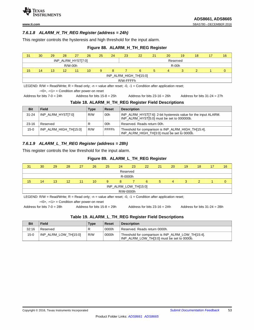
53
ADS8661, ADS8665www.ti.com SBAS780 –DECEMBER 2016
Product Folder Links: ADS8661 ADS8665
Submit Documentation FeedbackCopyright © 2016, Texas Instruments Incorporated
7.6.1.8 ALARM_H_TH_REG Register (address = 24h)This register controls the hysteresis and high threshold for the input alarm.
Figure 88. ALARM_H_TH_REG Register
31 30 29 28 27 26 25 24 23 22 21 20 19 18 17 16INP_ALRM_HYST[7:0] Reserved
R/W-00h R-00h15 14 13 12 11 10 9 8 7 6 5 4 3 2 1 0
INP_ALRM_HIGH_TH[15:0]R/W-FFFFh
LEGEND: R/W = Read/Write; R = Read only; -n = value after reset; -0, -1 = Condition after application reset;LEGEND: -<0>, -<1> = Condition after power-on resetAddress for bits 7-0 = 24h Address for bits 15-8 = 25h Address for bits 23-16 = 26h Address for bits 31-24 = 27h
Table 18. ALARM_H_TH_REG Register Field DescriptionsBit Field Type Reset Description
31-24 INP_ALRM_HYST[7:0] R/W 00h INP_ALRM_HYST[7:6]: 2-bit hysteresis value for the input ALARM.INP_ALRM_HYST[5:0] must be set to 000000b.
23-16 Reserved R 00h Reserved. Reads return 00h.15-0 INP_ALRM_HIGH_TH[15:0] R/W FFFFh Threshold for comparison is INP_ALRM_HIGH_TH[15:4].
INP_ALRM_HIGH_TH[3:0] must be set to 0000b.
7.6.1.9 ALARM_L_TH_REG Register (address = 28h)This register controls the low threshold for the input alarm.
Figure 89. ALARM_L_TH_REG Register
31 30 29 28 27 26 25 24 23 22 21 20 19 18 17 16ReservedR-0000h
15 14 13 12 11 10 9 8 7 6 5 4 3 2 1 0INP_ALRM_LOW_TH[15:0]
R/W-0000hLEGEND: R/W = Read/Write; R = Read only; -n = value after reset; -0, -1 = Condition after application reset;LEGEND: -<0>, -<1> = Condition after power-on resetAddress for bits 7-0 = 28h Address for bits 15-8 = 29h Address for bits 23-16 = 2Ah Address for bits 31-24 = 2Bh
Table 19. ALARM_L_TH_REG Register Field DescriptionsBit Field Type Reset Description
32:16 Reserved R 0000h Reserved. Reads return 0000h.15-0 INP_ALRM_LOW_TH[15:0] R/W 0000h Threshold for comparison is INP_ALRM_LOW_TH[15:4].
INP_ALRM_LOW_TH[3:0] must be set to 0000b.

SAR ADC Digital Host
Local Power Supply System Power Supply
xxxxxxxx
Isolated DC-DC
Converter
GND
IGND GNDGND
Digital IsolatorInput Signal
IsolationBarrier
IGND
IGND
VINP
VINM
GNDIGND
54
ADS8661, ADS8665SBAS780 –DECEMBER 2016 www.ti.com
Product Folder Links: ADS8661 ADS8665
Submit Documentation Feedback Copyright © 2016, Texas Instruments Incorporated
8 Application and Implementation
NOTEInformation in the following applications sections is not part of the TI componentspecification, and TI does not warrant its accuracy or completeness. TI’s customers areresponsible for determining suitability of components for their purposes. Customers shouldvalidate and test their design implementation to confirm system functionality.
8.1 Application InformationThe ADS866x is a fully-integrated data acquisition (DAQ) system based on a 12-bit successive approximation(SAR) analog-to-digital converter (ADC). The device includes an integrated analog front-end (AFE) circuit to drivethe inputs of the ADC and an integrated precision reference with a buffer. As such, this device does not requireany additional external circuits for driving the reference or analog input pins of the ADC.
8.2 Typical Application
NOTE: The potential difference between IGND and GND can be as high as the barrier breakdown voltage (often thousandsof volts).
Figure 90. 12-Bit Isolated DAQ System for High Common-Mode Rejection
8.2.1 Design RequirementsDesign a 12-bit DAQ system for processing input signals up to ±12 V superimposed on large dc or ac common-mode offsets relative to the ground potential of the system main power supply. The specific performancerequirements are as follows:• Input signal: ±12-V amplitude signal of a 1-kHz frequency superimposed on a ±75-V common-mode with
frequency between dc and 15 kHz• CMRR > 100 dB over stipulated common-mode frequency range• SNR > 70 dB• THD < –96 dB

Main Power Supply (> 4.3 V)
GND
Transformer Driver
xxxxxxxx
Isolation Barrier
IGND IGND
Full-Wave Rectifier and Smoothing Capacitor
IGNDGND VIN
GND
VIN VOUT Isolated 5 V
Isolated Switching Power Supply
S2
S1
1:NS (>1)
GND IGND
D1
D2
CS
M
IGND
GND
VIN VOUT Isolated 3.3 V
LDO
LDO
55
ADS8661, ADS8665www.ti.com SBAS780 –DECEMBER 2016
Product Folder Links: ADS8661 ADS8665
Submit Documentation FeedbackCopyright © 2016, Texas Instruments Incorporated
Typical Application (continued)8.2.2 Detailed Design ProcedureThe design uses galvanic isolation between the DAQ system inputs and main power supply to achieve extremelyhigh CMRR, as indicated by Figure 90. The system not only tolerates large common-mode voltages beyond itsabsolute maximum ratings but also delivers excellent performance largely independent of common-modeamplitude and frequency (within the specified operating limits). The relevant performance characteristics areillustrated in Figure 96, Figure 92, and Figure 93.
The system performance requirements by itself can be easily satisfied by using the ADS866x. This devicesimplifies system design because the ADS866x eliminates the need for designing a discrete high-performancesignal chain needed with most other SAR ADCs. In addition, the use of galvanic isolation has the followingsystem design implications:• A local floating supply is needed to power the ADS866x because the device cannot load the system main
power supply• A digital isolator is required to facilitate data transfer between the isolated ADS866x serial interface and the
digital host controller
The floating power supply can be realized as an isolated transformer-based, push-pull converter followed by arectifier and low-dropout (LDO) regulator to largely eliminate the ADC power-supply ripple by taking advantage ofthe high PSRR provided by most LDOs. A schematic of this design is shown in Figure 91.
Figure 91. Isolated Power-Supply Design
Recommended components for the circuit shown in Figure 91 are given below:• The SN6501 transformer driver is selected for its low input voltage requirement, small form-factor, and the
flexibility offered for easily adjusting the system isolation voltage rating by substituting the transformer• A miniature printed circuit board (PCB)-mount, center-tapped transformer with a gain > 1 maintains line
regulation at the LDO outputs• Schottky rectifiers for minimal forward voltage drop• Smoothing capacitor for sufficiently low ripple at the LDO input• The TPS7A4901 LDOs for an ultra-low noise contribution relative to the ADS866x and high PSRR over a
wide frequency range to attenuate output ripple to levels below the LDO output noise level
With regard to the digital isolator, the ISO7640FM is recommended for the following reasons:• Supports > a 50-MHz SCLK and the required logic levels for operating the ADS866x at the full throughput• Quad-channel device that facilitates excellent delay-matching between critical interface signals for reliable
operation at high speed
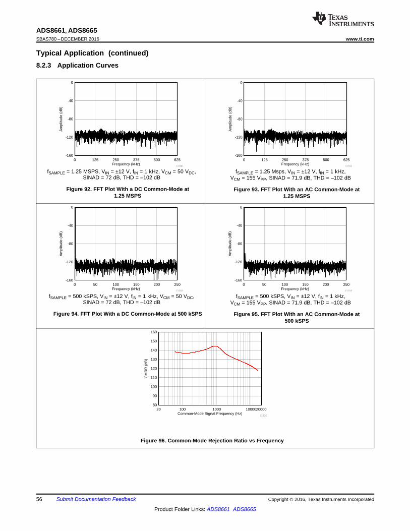
Common-Mode Signal Frequency (Hz)
CM
RR
(dB
)
20 100 1000 100002000080
90
100
110
120
130
140
150
160
D200
Frequency (kHz)
Am
plitu
de (
dB)
0 50 100 150 200 250-160
-120
-80
-40
0
D702Frequency (kHz)
Am
plitu
de (
dB)
0 50 100 150 200 250-160
-120
-80
-40
0
D703
Frequency (kHz)
Am
plitu
de (
dB)
0 125 250 375 500 625-160
-120
-80
-40
0
D700Frequency (kHz)
Am
plitu
de (
dB)
0 125 250 375 500 625-160
-120
-80
-40
0
D701
56
ADS8661, ADS8665SBAS780 –DECEMBER 2016 www.ti.com
Product Folder Links: ADS8661 ADS8665
Submit Documentation Feedback Copyright © 2016, Texas Instruments Incorporated
Typical Application (continued)8.2.3 Application Curves
fSAMPLE = 1.25 MSPS, VIN = ±12 V, fIN = 1 kHz, VCM = 50 VDC,SINAD = 72 dB, THD = –102 dB
Figure 92. FFT Plot With a DC Common-Mode at1.25 MSPS
fSAMPLE = 1.25 Msps, VIN = ±12 V, fIN = 1 kHz,VCM = 155 VPP, SINAD = 71.9 dB, THD = –102 dB
Figure 93. FFT Plot With an AC Common-Mode at1.25 MSPS
fSAMPLE = 500 kSPS, VIN = ±12 V, fIN = 1 kHz, VCM = 50 VDC,SINAD = 72 dB, THD = –102 dB
Figure 94. FFT Plot With a DC Common-Mode at 500 kSPS
fSAMPLE = 500 kSPS, VIN = ±12 V, fIN = 1 kHz,VCM = 155 VPP, SINAD = 71.9 dB, THD = –102 dB
Figure 95. FFT Plot With an AC Common-Mode at500 kSPS
Figure 96. Common-Mode Rejection Ratio vs Frequency
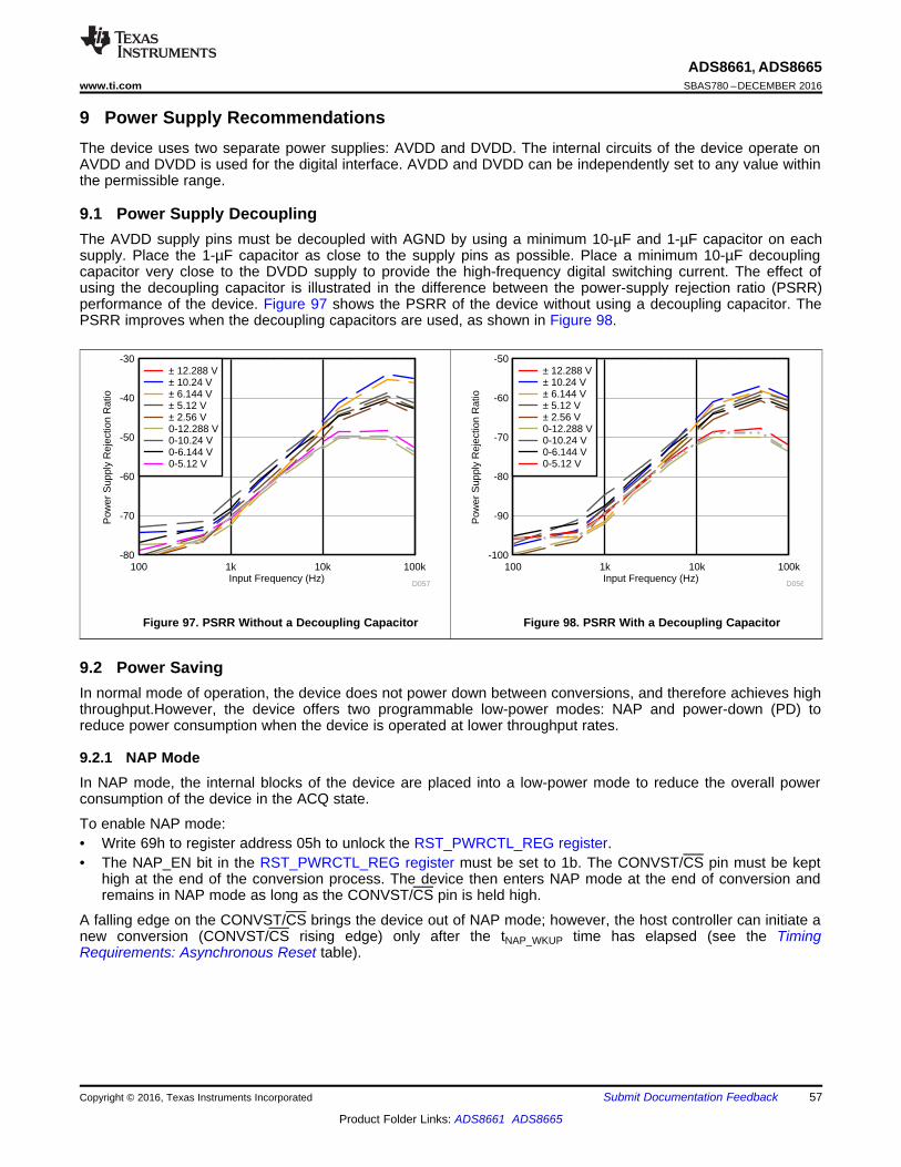
Input Frequency (Hz)
Pow
er S
uppl
y R
ejec
tion
Rat
io
-80
-70
-60
-50
-40
-30
100 1k 10k 100k
D057
± 12.288 V± 10.24 V± 6.144 V± 5.12 V± 2.56 V0-12.288 V0-10.24 V0-6.144 V0-5.12 V
Input Frequency (Hz)
Pow
er S
uppl
y R
ejec
tion
Rat
io
-100
-90
-80
-70
-60
-50
100 1k 10k 100k
D056
± 12.288 V± 10.24 V± 6.144 V± 5.12 V± 2.56 V0-12.288 V0-10.24 V0-6.144 V0-5.12 V
57
ADS8661, ADS8665www.ti.com SBAS780 –DECEMBER 2016
Product Folder Links: ADS8661 ADS8665
Submit Documentation FeedbackCopyright © 2016, Texas Instruments Incorporated
9 Power Supply RecommendationsThe device uses two separate power supplies: AVDD and DVDD. The internal circuits of the device operate onAVDD and DVDD is used for the digital interface. AVDD and DVDD can be independently set to any value withinthe permissible range.
9.1 Power Supply DecouplingThe AVDD supply pins must be decoupled with AGND by using a minimum 10-µF and 1-µF capacitor on eachsupply. Place the 1-µF capacitor as close to the supply pins as possible. Place a minimum 10-µF decouplingcapacitor very close to the DVDD supply to provide the high-frequency digital switching current. The effect ofusing the decoupling capacitor is illustrated in the difference between the power-supply rejection ratio (PSRR)performance of the device. Figure 97 shows the PSRR of the device without using a decoupling capacitor. ThePSRR improves when the decoupling capacitors are used, as shown in Figure 98.
Figure 97. PSRR Without a Decoupling Capacitor Figure 98. PSRR With a Decoupling Capacitor
9.2 Power SavingIn normal mode of operation, the device does not power down between conversions, and therefore achieves highthroughput.However, the device offers two programmable low-power modes: NAP and power-down (PD) toreduce power consumption when the device is operated at lower throughput rates.
9.2.1 NAP ModeIn NAP mode, the internal blocks of the device are placed into a low-power mode to reduce the overall powerconsumption of the device in the ACQ state.
To enable NAP mode:• Write 69h to register address 05h to unlock the RST_PWRCTL_REG register.• The NAP_EN bit in the RST_PWRCTL_REG register must be set to 1b. The CONVST/CS pin must be kept
high at the end of the conversion process. The device then enters NAP mode at the end of conversion andremains in NAP mode as long as the CONVST/CS pin is held high.
A falling edge on the CONVST/CS brings the device out of NAP mode; however, the host controller can initiate anew conversion (CONVST/CS rising edge) only after the tNAP_WKUP time has elapsed (see the TimingRequirements: Asynchronous Reset table).

58
ADS8661, ADS8665SBAS780 –DECEMBER 2016 www.ti.com
Product Folder Links: ADS8661 ADS8665
Submit Documentation Feedback Copyright © 2016, Texas Instruments Incorporated
Power Saving (continued)9.2.2 Power-Down (PD) ModeThe device also features a deep power-down mode (PD) to reduce the power consumption at very lowthroughput rates.
The following steps must be taken to enter PD mode:1. Write 69h to register address 05h to unlock the RST_PWRCTL_REG register.2. Set the PWRDN bit in the RST_PWRCTL_REG register to 1b. The device enters PD mode on the rising
edge of the CONVST/CS signal.
In PD mode, all analog blocks within the device are powered down; however, the interface remains active andthe register contents are also retained. The RVS pin is high, indicating that the device is ready to receive thenext command.
In order to exit PD mode:1. Clear the PWRDN bit in the RST_PWRCTL_REG register to 0b.2. The RVS pin goes high, indicating that the device has started coming out of PD mode. However, the host
controller must wait for the tPWRUP time (see the Timing Requirements: Asynchronous Reset table) to elapsebefore initiating a new conversion.
10 Layout
10.1 Layout GuidelinesFigure 99 illustrates a PCB layout example for the ADS866x.• Partition the PCB into analog and digital sections. Care must be taken to ensure that the analog signals are
kept away from the digital lines. This layout helps keep the analog input and reference input signals awayfrom the digital noise. In this layout example, the analog input and reference signals are routed on the lowerside of the board and the digital connections are routed on the top side of the board.
• Using a single dedicated ground plane is strongly encouraged.• Power sources to the ADS866x must be clean and well-bypassed. Using a 1-μF, X7R-grade, 0603-size
ceramic capacitor with at least a 10-V rating in close proximity to the analog (AVDD) supply pins isrecommended. For decoupling the digital supply pin (DVDD), a 1-μF, X7R-grade, 0603-size ceramic capacitorwith at least a 10-V rating is recommended. Placing vias between the AVDD, DVDD pins and the bypasscapacitors must be avoided. All ground pins must be connected to the ground plane using short, low-impedance paths.
• There are two decoupling capacitors used for the REFCAP pin. The first is a small, 1-μF, 0603-size ceramiccapacitor placed close to the device pins for decoupling the high-frequency signals and the second is a10-μF, 0805-size ceramic capacitor to provide the charge required by the reference circuit of the device. Acapacitor with an ESR less than 0.2 Ω is recommended for the 10-μF capacitor. Both of these capacitorsmust be directly connected to the device pins without any vias between the pins and capacitors.
• The REFIO pin also must be decoupled with a minimum of 4.7-μF ceramic capacitor if the internal referenceof the device is used. The capacitor must be placed close to the device pins.
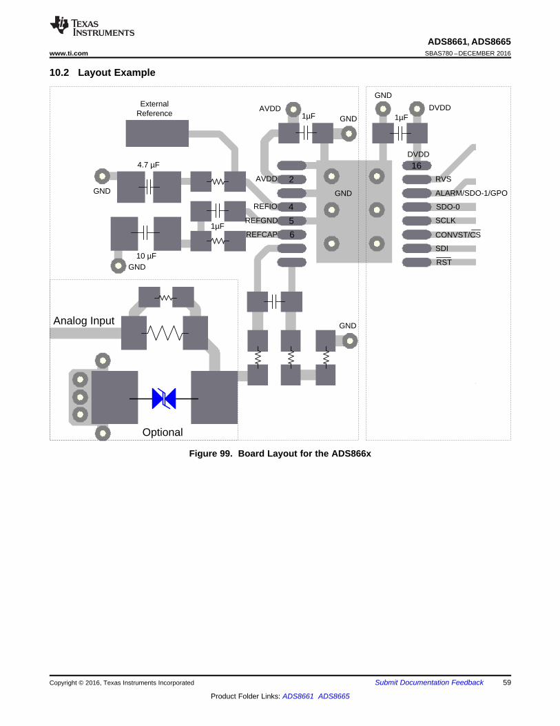
4
5
2
6
16
REFGND
GND
REFIO
REFCAP
AVDD
DVDD
SDI
SCLK
SDO-0
CONVST/CS
RST
ALARM/SDO-1/GPO
RVS
1µF
10 µF
4.7 µF
1µF
1µF
Optional
Analog Input
AVDD
GND
GND
GND
GND
GND
DVDDExternal Reference
59
ADS8661, ADS8665www.ti.com SBAS780 –DECEMBER 2016
Product Folder Links: ADS8661 ADS8665
Submit Documentation FeedbackCopyright © 2016, Texas Instruments Incorporated
10.2 Layout Example
Figure 99. Board Layout for the ADS866x
60
ADS8661, ADS8665SBAS780 –DECEMBER 2016 www.ti.com
Product Folder Links: ADS8661 ADS8665
Submit Documentation Feedback Copyright © 2016, Texas Instruments Incorporated
11 Device and Documentation Support
11.1 Documentation Support
11.1.1 Related DocumentationFor related documentation see the following:• OPA320 Precision, 20MHz, 0.9pA, Low-Noise, RRIO, CMOS Operational Amplifier with Shutdown
(SBOS513)• SN6501 Transformer Driver for Isolated Power Supplies (SLLSEA0)• TPS7A49 36-V, 150-mA, Ultralow-Noise, Positive Linear Regulator (SBVS121)• ISO764xFM Low-Power Quad-Channel Digital Isolators (SLLSE89)• AN-2029 Handling and Process Recommendations Application Report (SNOA550)
11.2 Related LinksThe table below lists quick access links. Categories include technical documents, support and communityresources, tools and software, and quick access to sample or buy.
Table 20. Related Links
PARTS PRODUCT FOLDER SAMPLE & BUY TECHNICALDOCUMENTS
TOOLS &SOFTWARE
SUPPORT &COMMUNITY
ADS8661 Click here Click here Click here Click here Click hereADS8665 Click here Click here Click here Click here Click here
11.3 Receiving Notification of Documentation UpdatesTo receive notification of documentation updates, navigate to the device product folder on ti.com. In the upperright corner, click on Alert me to register and receive a weekly digest of any product information that haschanged. For change details, review the revision history included in any revised document.
11.4 Community ResourcesThe following links connect to TI community resources. Linked contents are provided "AS IS" by the respectivecontributors. They do not constitute TI specifications and do not necessarily reflect TI's views; see TI's Terms ofUse.
TI E2E™ Online Community TI's Engineer-to-Engineer (E2E) Community. Created to foster collaborationamong engineers. At e2e.ti.com, you can ask questions, share knowledge, explore ideas and helpsolve problems with fellow engineers.
Design Support TI's Design Support Quickly find helpful E2E forums along with design support tools andcontact information for technical support.
11.5 TrademarksE2E is a trademark of Texas Instruments.multiSPI is a trademark of Motorola Mobility LLC.All other trademarks are the property of their respective owners.
11.6 Electrostatic Discharge CautionThis integrated circuit can be damaged by ESD. Texas Instruments recommends that all integrated circuits be handled withappropriate precautions. Failure to observe proper handling and installation procedures can cause damage.
ESD damage can range from subtle performance degradation to complete device failure. Precision integrated circuits may be moresusceptible to damage because very small parametric changes could cause the device not to meet its published specifications.
11.7 GlossarySLYZ022 — TI Glossary.
This glossary lists and explains terms, acronyms, and definitions.

61
ADS8661, ADS8665www.ti.com SBAS780 –DECEMBER 2016
Product Folder Links: ADS8661 ADS8665
Submit Documentation FeedbackCopyright © 2016, Texas Instruments Incorporated
12 Mechanical, Packaging, and Orderable InformationThe following pages include mechanical, packaging, and orderable information. This information is the mostcurrent data available for the designated devices. This data is subject to change without notice and revision ofthis document. For browser-based versions of this data sheet, refer to the left-hand navigation.

PACKAGE OPTION ADDENDUM
www.ti.com 13-Jun-2018
Addendum-Page 1
PACKAGING INFORMATION
Orderable Device Status(1)
Package Type PackageDrawing
Pins PackageQty
Eco Plan(2)
Lead/Ball Finish(6)
MSL Peak Temp(3)
Op Temp (°C) Device Marking(4/5)
Samples
ADS8661IPW ACTIVE TSSOP PW 16 90 Green (RoHS& no Sb/Br)
CU NIPDAU Level-3-260C-168 HR -40 to 125 ADS8661
ADS8661IPWR ACTIVE TSSOP PW 16 2000 Green (RoHS& no Sb/Br)
CU NIPDAU Level-3-260C-168 HR -40 to 125 ADS8661
ADS8665IPW ACTIVE TSSOP PW 16 90 Green (RoHS& no Sb/Br)
CU NIPDAU Level-3-260C-168 HR -40 to 125 ADS8665
ADS8665IPWR ACTIVE TSSOP PW 16 2000 Green (RoHS& no Sb/Br)
CU NIPDAU Level-3-260C-168 HR -40 to 125 ADS8665
(1) The marketing status values are defined as follows:ACTIVE: Product device recommended for new designs.LIFEBUY: TI has announced that the device will be discontinued, and a lifetime-buy period is in effect.NRND: Not recommended for new designs. Device is in production to support existing customers, but TI does not recommend using this part in a new design.PREVIEW: Device has been announced but is not in production. Samples may or may not be available.OBSOLETE: TI has discontinued the production of the device.
(2) RoHS: TI defines "RoHS" to mean semiconductor products that are compliant with the current EU RoHS requirements for all 10 RoHS substances, including the requirement that RoHS substancedo not exceed 0.1% by weight in homogeneous materials. Where designed to be soldered at high temperatures, "RoHS" products are suitable for use in specified lead-free processes. TI mayreference these types of products as "Pb-Free".RoHS Exempt: TI defines "RoHS Exempt" to mean products that contain lead but are compliant with EU RoHS pursuant to a specific EU RoHS exemption.Green: TI defines "Green" to mean the content of Chlorine (Cl) and Bromine (Br) based flame retardants meet JS709B low halogen requirements of <=1000ppm threshold. Antimony trioxide basedflame retardants must also meet the <=1000ppm threshold requirement.
(3) MSL, Peak Temp. - The Moisture Sensitivity Level rating according to the JEDEC industry standard classifications, and peak solder temperature.
(4) There may be additional marking, which relates to the logo, the lot trace code information, or the environmental category on the device.
(5) Multiple Device Markings will be inside parentheses. Only one Device Marking contained in parentheses and separated by a "~" will appear on a device. If a line is indented then it is a continuationof the previous line and the two combined represent the entire Device Marking for that device.
(6) Lead/Ball Finish - Orderable Devices may have multiple material finish options. Finish options are separated by a vertical ruled line. Lead/Ball Finish values may wrap to two lines if the finishvalue exceeds the maximum column width.
Important Information and Disclaimer:The information provided on this page represents TI's knowledge and belief as of the date that it is provided. TI bases its knowledge and belief on informationprovided by third parties, and makes no representation or warranty as to the accuracy of such information. Efforts are underway to better integrate information from third parties. TI has taken and

PACKAGE OPTION ADDENDUM
www.ti.com 13-Jun-2018
Addendum-Page 2
continues to take reasonable steps to provide representative and accurate information but may not have conducted destructive testing or chemical analysis on incoming materials and chemicals.TI and TI suppliers consider certain information to be proprietary, and thus CAS numbers and other limited information may not be available for release.
In no event shall TI's liability arising out of such information exceed the total purchase price of the TI part(s) at issue in this document sold by TI to Customer on an annual basis.
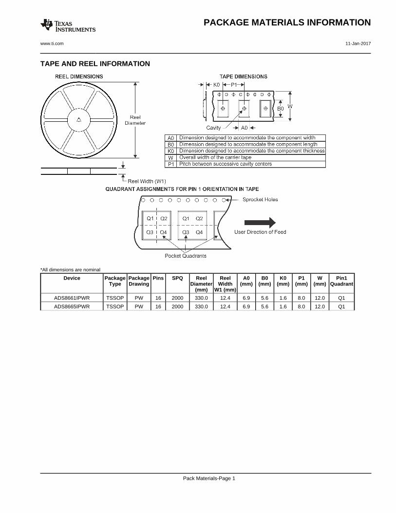
TAPE AND REEL INFORMATION
*All dimensions are nominal
Device PackageType
PackageDrawing
Pins SPQ ReelDiameter
(mm)
ReelWidth
W1 (mm)
A0(mm)
B0(mm)
K0(mm)
P1(mm)
W(mm)
Pin1Quadrant
ADS8661IPWR TSSOP PW 16 2000 330.0 12.4 6.9 5.6 1.6 8.0 12.0 Q1
ADS8665IPWR TSSOP PW 16 2000 330.0 12.4 6.9 5.6 1.6 8.0 12.0 Q1
PACKAGE MATERIALS INFORMATION
www.ti.com 11-Jan-2017
Pack Materials-Page 1
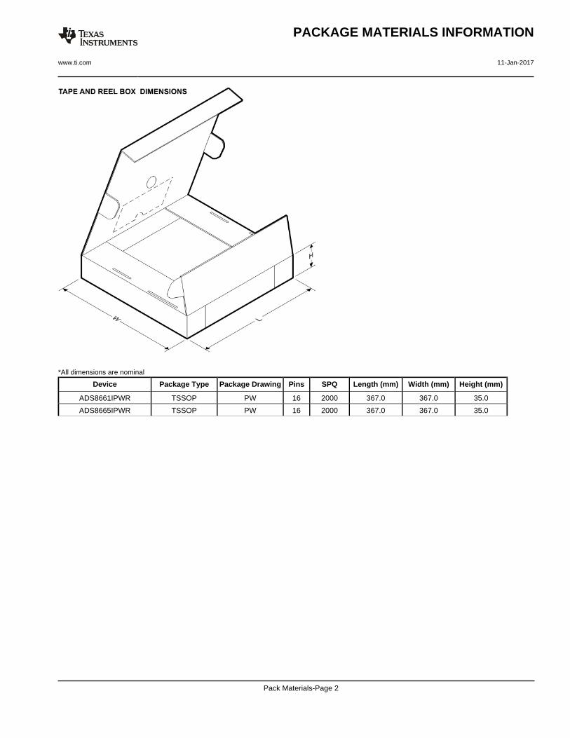
*All dimensions are nominal
Device Package Type Package Drawing Pins SPQ Length (mm) Width (mm) Height (mm)
ADS8661IPWR TSSOP PW 16 2000 367.0 367.0 35.0
ADS8665IPWR TSSOP PW 16 2000 367.0 367.0 35.0
PACKAGE MATERIALS INFORMATION
www.ti.com 11-Jan-2017
Pack Materials-Page 2


IMPORTANT NOTICE
Texas Instruments Incorporated (TI) reserves the right to make corrections, enhancements, improvements and other changes to itssemiconductor products and services per JESD46, latest issue, and to discontinue any product or service per JESD48, latest issue. Buyersshould obtain the latest relevant information before placing orders and should verify that such information is current and complete.TI’s published terms of sale for semiconductor products (http://www.ti.com/sc/docs/stdterms.htm) apply to the sale of packaged integratedcircuit products that TI has qualified and released to market. Additional terms may apply to the use or sale of other types of TI products andservices.Reproduction of significant portions of TI information in TI data sheets is permissible only if reproduction is without alteration and isaccompanied by all associated warranties, conditions, limitations, and notices. TI is not responsible or liable for such reproduceddocumentation. Information of third parties may be subject to additional restrictions. Resale of TI products or services with statementsdifferent from or beyond the parameters stated by TI for that product or service voids all express and any implied warranties for theassociated TI product or service and is an unfair and deceptive business practice. TI is not responsible or liable for any such statements.Buyers and others who are developing systems that incorporate TI products (collectively, “Designers”) understand and agree that Designersremain responsible for using their independent analysis, evaluation and judgment in designing their applications and that Designers havefull and exclusive responsibility to assure the safety of Designers' applications and compliance of their applications (and of all TI productsused in or for Designers’ applications) with all applicable regulations, laws and other applicable requirements. Designer represents that, withrespect to their applications, Designer has all the necessary expertise to create and implement safeguards that (1) anticipate dangerousconsequences of failures, (2) monitor failures and their consequences, and (3) lessen the likelihood of failures that might cause harm andtake appropriate actions. Designer agrees that prior to using or distributing any applications that include TI products, Designer willthoroughly test such applications and the functionality of such TI products as used in such applications.TI’s provision of technical, application or other design advice, quality characterization, reliability data or other services or information,including, but not limited to, reference designs and materials relating to evaluation modules, (collectively, “TI Resources”) are intended toassist designers who are developing applications that incorporate TI products; by downloading, accessing or using TI Resources in anyway, Designer (individually or, if Designer is acting on behalf of a company, Designer’s company) agrees to use any particular TI Resourcesolely for this purpose and subject to the terms of this Notice.TI’s provision of TI Resources does not expand or otherwise alter TI’s applicable published warranties or warranty disclaimers for TIproducts, and no additional obligations or liabilities arise from TI providing such TI Resources. TI reserves the right to make corrections,enhancements, improvements and other changes to its TI Resources. TI has not conducted any testing other than that specificallydescribed in the published documentation for a particular TI Resource.Designer is authorized to use, copy and modify any individual TI Resource only in connection with the development of applications thatinclude the TI product(s) identified in such TI Resource. NO OTHER LICENSE, EXPRESS OR IMPLIED, BY ESTOPPEL OR OTHERWISETO ANY OTHER TI INTELLECTUAL PROPERTY RIGHT, AND NO LICENSE TO ANY TECHNOLOGY OR INTELLECTUAL PROPERTYRIGHT OF TI OR ANY THIRD PARTY IS GRANTED HEREIN, including but not limited to any patent right, copyright, mask work right, orother intellectual property right relating to any combination, machine, or process in which TI products or services are used. Informationregarding or referencing third-party products or services does not constitute a license to use such products or services, or a warranty orendorsement thereof. Use of TI Resources may require a license from a third party under the patents or other intellectual property of thethird party, or a license from TI under the patents or other intellectual property of TI.TI RESOURCES ARE PROVIDED “AS IS” AND WITH ALL FAULTS. TI DISCLAIMS ALL OTHER WARRANTIES ORREPRESENTATIONS, EXPRESS OR IMPLIED, REGARDING RESOURCES OR USE THEREOF, INCLUDING BUT NOT LIMITED TOACCURACY OR COMPLETENESS, TITLE, ANY EPIDEMIC FAILURE WARRANTY AND ANY IMPLIED WARRANTIES OFMERCHANTABILITY, FITNESS FOR A PARTICULAR PURPOSE, AND NON-INFRINGEMENT OF ANY THIRD PARTY INTELLECTUALPROPERTY RIGHTS. TI SHALL NOT BE LIABLE FOR AND SHALL NOT DEFEND OR INDEMNIFY DESIGNER AGAINST ANY CLAIM,INCLUDING BUT NOT LIMITED TO ANY INFRINGEMENT CLAIM THAT RELATES TO OR IS BASED ON ANY COMBINATION OFPRODUCTS EVEN IF DESCRIBED IN TI RESOURCES OR OTHERWISE. IN NO EVENT SHALL TI BE LIABLE FOR ANY ACTUAL,DIRECT, SPECIAL, COLLATERAL, INDIRECT, PUNITIVE, INCIDENTAL, CONSEQUENTIAL OR EXEMPLARY DAMAGES INCONNECTION WITH OR ARISING OUT OF TI RESOURCES OR USE THEREOF, AND REGARDLESS OF WHETHER TI HAS BEENADVISED OF THE POSSIBILITY OF SUCH DAMAGES.Unless TI has explicitly designated an individual product as meeting the requirements of a particular industry standard (e.g., ISO/TS 16949and ISO 26262), TI is not responsible for any failure to meet such industry standard requirements.Where TI specifically promotes products as facilitating functional safety or as compliant with industry functional safety standards, suchproducts are intended to help enable customers to design and create their own applications that meet applicable functional safety standardsand requirements. Using products in an application does not by itself establish any safety features in the application. Designers mustensure compliance with safety-related requirements and standards applicable to their applications. Designer may not use any TI products inlife-critical medical equipment unless authorized officers of the parties have executed a special contract specifically governing such use.Life-critical medical equipment is medical equipment where failure of such equipment would cause serious bodily injury or death (e.g., lifesupport, pacemakers, defibrillators, heart pumps, neurostimulators, and implantables). Such equipment includes, without limitation, allmedical devices identified by the U.S. Food and Drug Administration as Class III devices and equivalent classifications outside the U.S.TI may expressly designate certain products as completing a particular qualification (e.g., Q100, Military Grade, or Enhanced Product).Designers agree that it has the necessary expertise to select the product with the appropriate qualification designation for their applicationsand that proper product selection is at Designers’ own risk. Designers are solely responsible for compliance with all legal and regulatoryrequirements in connection with such selection.Designer will fully indemnify TI and its representatives against any damages, costs, losses, and/or liabilities arising out of Designer’s non-compliance with the terms and provisions of this Notice.
Mailing Address: Texas Instruments, Post Office Box 655303, Dallas, Texas 75265Copyright © 2018, Texas Instruments Incorporated