10 watt mmds packaged amplifier - media.digikey.com sheets/triquint/tga2924-sg.pdf · • 2.5% evm...
TRANSCRIPT

1
TGA2924-SG
May 2009 © Rev -
TriQuint Semiconductor: www. triquint.com (972)994-8465 Fax (972)994-8504 [email protected]
-25
-20
-15
-10
-5
0
5
10
15
2 2.1 2.2 2.3 2.4 2.5 2.6 2.7 2.8 2.9 3
Frequency (GHz)
S-Pa
ram
eter
(dB
)
Key Features• 2. 6 GHz Application Frequency Range• 12 dB Nominal Gain • 40 dBm Nominal Psat• 2.5% EVM at 30 dBm output power• Internally Partially Matched• IMD3 -45 dBc @ 28 dBm SCL, Typical• Bias Conditions: 8 V @ 1.2 A (Quiescent)• 0.5 μm HFET Technology• 2 lead Cu-alloy base package
Fixtured Measured PerformanceBias Conditions: Vd = 8 V, Idq =1.2 A
Performance data taken in a 2.6 GHz application circuit
Primary Applications• MMDS Pt-Pt and Pt-Multi Pt Radio• S-Band Power Amplifiers
The TGA2924-SG HPA provides 12 dB of gain, 10 W of output power at 2.6 GHz and 2.5% EVM at 30 dBm output power. The device is ideally suited for high linearity, high power wireless data applications such as MMDS Point-to-Point or Point-to-Multi-Point radios. The package has a high thermal conductivity copper alloy base. Internal partial matching simplifies system board layout by requiring a minimum of external components.
Lead-Free & RoHS compliant.
Evaluation Boards are available.
Product Description
S21
S11
S22
35.536
36.537
37.538
38.539
39.540
40.5
2.4 2.45 2.5 2.55 2.6 2.65 2.7 2.75 2.8
Frequency (GHz)
Out
put P
ower
(dB
m)
P1dB
P2dB
10 Watt MMDS Packaged Amplifier
Datasheet subject to change without notice

2
TGA2924-SG
May 2009 © Rev -
TriQuint Semiconductor: www. triquint.com (972)994-8465 Fax (972)994-8504 [email protected]
TABLE I MAXIMUM RATINGS 1/
Symbol Parameter Value Notes
Vd Drain Supply Voltage 10 V 2/
Vg Gate Supply Voltage Range 0 V to -5 V
Idq Drain Supply Current (Quiescent) 4 A 2/
| Ig | Gate Current 39 mA
PIN Input Continuous Wave Power 39 dBm 2/
PD Power Dissipation 14.4 W 2/, 3/
TCH Operating Channel Temperature 200 °C 4/
Mounting Temperature (30 Seconds) 260 °C
TSTG Storage Temperature -65 to 150 °C 1/ These ratings represent the maximum operable values for this device.
2/ Combinations of supply voltage, supply current, input power, and output power shall not exceed PD.
3/ When operated at this bias condition with a base plate temperature of 85 °C, the median life is 7.5E5 hours.
4/ Junction operating temperature will directly affect the device median time to failure (Tm). For maximum life, it is recommended that junction temperatures be maintained at the lowest possible levels.

3
TGA2924-SG
May 2009 © Rev -
TriQuint Semiconductor: www. triquint.com (972)994-8465 Fax (972)994-8504 [email protected]
TABLE IIRF CHARACTERIZATION TABLE
(TA = 25°C, Nominal)(Vd = 8 V, Idq = 1.2 A)
SYMBOL PARAMETER TESTCONDITION TYPICAL UNITS
Gain Small Signal Gain f = 2.6 GHz 12 dB
IRL Input Return Loss f = 2.6 GHz 6 dB
ORL Output Return Loss f = 2.6 GHz 10 dB
Psat Saturated Output Power 40 dBm

4
TGA2924-SG
May 2009 © Rev -
TriQuint Semiconductor: www. triquint.com (972)994-8465 Fax (972)994-8504 [email protected]
TABLE III THERMAL INFORMATION
Parameter Test Conditions TCH (°C)
θJC (°C/W)
Tm (HRS)
θJC Thermal Resistance (channel to backside of package)
Vd = 8 V ID = 1.2 A Pdiss = 9.6 W
162
8
3.5 E+7
Note: Package backside SnPb soldered to carrier at 85 °C baseplate temperature. At saturated output power, the DC power consumption is 20W with 10W RF power delivered to the load and 10W dissipated. Adding the 1W RF input power results in 11W total power dissipation and a maximum channel temperature of 173 °C at 85 °C baseplate temperature.
Median Lifetime (Tm) vs. Channel Temperature

5
TGA2924-SG
May 2009 © Rev -
TriQuint Semiconductor: www. triquint.com (972)994-8465 Fax (972)994-8504 [email protected]
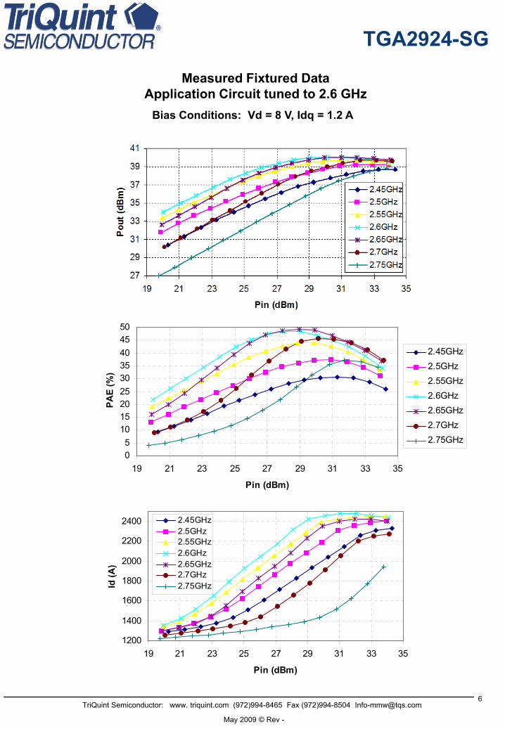
Bias Conditions: Vd = 8 V, Idq = 1.2 A
Measured Fixtured DataApplication Circuit tuned to 2.6 GHz
6
TGA2924-SG
May 2009 © Rev -
TriQuint Semiconductor: www. triquint.com (972)994-8465 Fax (972)994-8504 [email protected]
Bias Conditions: Vd = 8 V, Idq = 1.2 A
Measured Fixtured DataApplication Circuit tuned to 2.6 GHz
05
101520253035404550
19 21 23 25 27 29 31 33 35
Pin (dBm)
PAE
(%)
2.45GHz2.5GHz2.55GHz2.6GHz2.65GHz2.7GHz2.75GHz
1200
1400
1600
1800
2000
2200
2400
19 21 23 25 27 29 31 33 35
Pin (dBm)
Id (A
)
2.45GHz2.5GHz2.55GHz2.6GHz2.65GHz2.7GHz2.75GHz

7
TGA2924-SG
May 2009 © Rev -
TriQuint Semiconductor: www. triquint.com (972)994-8465 Fax (972)994-8504 [email protected]
Bias Conditions: Vd = 8 V, Idq = 1.2 A
Measured Fixtured DataApplication Circuit tuned to 2.6 GHz

8
TGA2924-SG
May 2009 © Rev -
TriQuint Semiconductor: www. triquint.com (972)994-8465 Fax (972)994-8504 [email protected]
Bias Conditions: Vd = 8 V, Idq = 1.2 A
Measured Fixtured DataApplication Circuit tuned to 2.6 GHz

9
TGA2924-SG
May 2009 © Rev -
TriQuint Semiconductor: www. triquint.com (972)994-8465 Fax (972)994-8504 [email protected]
Side View
Bias Procedure
1. Ensure no RF power is applied to the device.2. Pinch off device by setting Vg to –3V.3. Increase Vd to 8.0V while monitoring drain current.4. Increase Vg until drain current reaches 1.2A5. Apply RF power.
Mechanical Drawing
Top View
Note: All dimensions are in inches with ±5 mil tolerance
0.068
Vg Vd

10
TGA2924-SG
May 2009 © Rev -
TriQuint Semiconductor: www. triquint.com (972)994-8465 Fax (972)994-8504 [email protected]
2.6 GHz Application Circuit Schematic
PCB is 20 mil thick Rogers 4003 substrate

11
TGA2924-SG
May 2009 © Rev -
TriQuint Semiconductor: www. triquint.com (972)994-8465 Fax (972)994-8504 [email protected]
Typical Evaluation Board Layout *
*The layout is a general purpose drawing that needs to be tuned for the specific application.
PCB is RO4003 20 mil thickness, 0.5 oz standard copper cladding, with εr = 3.38.
Contact TriQuint Applications Engineering for additional info
External Component Listing
Part Type Reference Description
Capacitor C1 AVX 06035J5R6BBT, 5.6 pF
Capacitor C2 AVX 06035J5R6BBT, 5.6 pF
Capacitor C3 4.7uF
Capacitor C4 AVX 06035J8R2BBT, 8.2 pF
Capacitor C5 AVX 06035J8R2BBT, 8.2 pF
Resistor R1 0805, 10 Ω
C1 C2
C3
C4C5
R1
207 mil 518 mil
1095 mil
902 mil
Vg Vd
IN OUT

12
TGA2924-SG
May 2009 © Rev -
TriQuint Semiconductor: www. triquint.com (972)994-8465 Fax (972)994-8504 [email protected]
Recommended Surface Mount Package Assembly
Proper ESD precautions must be followed while handling packages.
Clean the board with acetone. Rinse with alcohol. Allow the circuit to fully dry.
TriQuint recommends using a conductive solder paste for attachment. Follow solder paste and reflow oven vendors’ recommendations when developing a solder reflow profile. Typical solder reflow profiles are listed in the table below.
Hand soldering is not recommended. Solder paste can be applied using a stencil printer or dot placement. The volume of solder paste depends on PCB and component layout and should be well controlled to ensure consistent mechanical and electrical performance.
Clean the assembly with alcohol.
Typical Solder Reflow Profiles
Reflow Profile SnPb Pb FreeRamp-up Rate 3 °C/sec 3 °C/sec
Activation Time andTemperature 60 – 120 sec @ 140 – 160 °C 60 – 180 sec @ 150 – 200 °C
Time above Melting Point 60 – 150 sec 60 – 150 sec
Max Peak Temperature 240 °C 260 °C
Time within 5 °C of PeakTemperature 10 – 20 sec 10 – 20 sec
Ramp-down Rate 4 – 6 °C/sec 4 – 6 °C/sec
Part Package StyleTGA2924-SG Gullwing Leads
Ordering Information