10 ghz microwave link 1 report.pdf · 10 ghz microwave link by david levine ... is set up by a...
TRANSCRIPT

10 GHz Microwave Link
By David Levine Collin Phelps
Michael Brown and
Nicholas Tsaparas
A Report submitted in partial fulfillment
of the requirements of ELEC 490
Concordia University November 2002

Table of Contents
1. INTRODUCTION 1
2. OBJECTIVE 2
3. SYSTEM DESIGN 5
3.1 The Antenna 5
3.2 The Gunnplexer 6
3.3 The Intermediate Frequency (IF) Strip 6
3.4 The FSK Demodulator 7
3.5 The Output Buffer 8
3.6 The FSK Modulator 9
3.7 The Attachment User Interface (AUI) 10
3.8 Tuning Considerations 10
4. TASKS COMPLETED 8
4.1 Design of Subsystems 8
4.1.1 FSK Modulator 8
4.1.2 Gunnplexer Assembly 8
4.1.3 IF Strip 9
4.1.4 FSK Demodulator 9
4.1.5 Output Buffer 9
4.1.6 The AFC Buffer 10
4.1.7 The S-Meter Circuits 10
4.1.8 Tuning / Fault Meter 10
4.2 Missing Elements 8
4.2.1 Missing Components 9
4.2.2 Incomplete Gunnplexer Assembly 10
4.2.3 Meters and AUI Ports 10
4.3 Encountered Problems 10
4.3.1 Isolation of Individual Modules 10
4.3.2 Mismatch in Sizing of MC-13155 and PCB Socket 10
4.4 Clarification of Last Year’s Final Report 11
4.4.1 Inconsistency in Bandwidth Calculations 11
4.4.2 Use of Tantalum Capacitors 11
4.4.3 Disregarding Resistors 11
4.4.4 Connection of AUI ports 11
4.4.5 The Role of the TCP/IP and MAC Protocol in Error Correction 11
4.4.6 Current Op-Amp 11
4.4.7 OSI Model 11
4.4.8 How Inductance Arises in a PCB 11

5. TASKS AT HAND 8
5.1 Completion of the Circuit Boards and Other Components 8
5.2 Testing the Operation of the Circuit Boards 8
5.2.1 Gunnplexer Frequency Calibration 9
5.2.2 FSK Demodulator Calibration 10
5.2.3 FSK Modulator Deviation Adjustment 10
5.2.4 Testing the IF Strip 11
5.2.5 Testing Transceivers in Loop-Back Mode 11
5.3 Testing the Entire System 10
5.3.1 Ethernet Applications 10
5.3.2 Design of Antennas 10
5.4 Other Possible Applications of 10 GHz Link 11
5.5 Summary and Breakdown of Tasks 11
5.5.1 Functionality of System 11
5.5.2 Application of System to Ethernet Network 11
5.5.3 Wireless Transmission 11
5.5.4 Further Experimentation 11
6. PARTS REQUIRED 12
7. CONCLUSION 12
REFERENCES 13
APPENDIX A: HOW THE AUI CONNECTOR WORKS 14
List of Figures
Fig. 1 Low Frequency Unit…….............................................................................3
Fig. 2 High Frequency Unit...................................................................................4
Fig. 3 15 Pin AUI Connector.................................................................................7
Fig. 4 Assembled PCB…………………………………...........................................9
List of Tables
Table 1 Task Allocation……...................................................................................27
Table 2 List of Parts and Tools Required...............................................................28
Table 3 AUI pin connections..................................................................................31
Table 4 Connection Between Two PC Ethernet Cards .........................................31

1. INTRODUCTION
Nowadays, there are many ways for two systems to communicate in a wireless
manner. Every different way has its own advantages and disadvantages. In this
project, we will be experimenting with a 10 GHz wireless microwave link system.
This system has many advantages over many widely used systems. Several of
the main advantages are bandwidth usage and potential range of operation.
The 10 GHz link system we will be implementing is based on a model designed
by John Miles [1]. The motivation John Miles had for creating the system he
created was to be able to remotely access his office’s high speed internet
connection from home for free. Hence, John Miles’ design is primarily geared
toward network applications, but the link can ultimately be used for many
applications.
This report will outline precisely what the project will entail as well as give a
description of how the overall system works and how it was designed.
1

2
2. OBJECTIVE
The objective of this project is to successfully implement, test, and apply a
working 10 GHz microwave communication link. A microwave link is a wireless
communication system that sends and receives information through the
conversion of electrical signals to propagating electric fields. An electrical signal
is set up by a transmitter and is coupled through a microwave network and
propagated into free space with the use of an antenna. The signal then travels
through space to a receiver. The receiver has an antenna that will pick up the
transmitted electric field and convert it back to an electric signal, which is then
interpreted by the receiver’s associated circuitry to recover the original signal.
Then, using a connection called an Attachment Unit Interface (AUI), the signal
is routed to a load device. The load device then uses the signal for whatever its
application may be. In this project, the first application we will implement is a
wireless Ethernet network. Beyond that application, we are hoping to be able to
experiment with other possible applications of the wireless link. The project will
be carried out in different stages, some of which have been completed to date.
Last year, a team of undergraduate students consisting of Benoît Chapelotte,
Dave M. Gunputhram and Damien Avril began work on this very project [2]. They
had hoped to get the wireless Ethernet network functional. Unfortunately, as shall
be explained, due to time constraints, they were unable to complete all that they
had hoped to. They did, however, manage to complete the design and most of
the assembly of the main components. Therefore our project will focus less on
the design of the system and more on the testing and implementation of it.
As mentioned, the system we are using is based on a design created by John
Miles [1] and uses most of the same components.

3
3. SYSTEM DESIGN
The overall microwave link will have two units: the low frequency transceiver unit
and the high frequency transceiver unit. The low and high reflect the frequencies
to which each unit is tuned. These frequencies are 10.178 GHz for the low
frequency unit and 10.323 GHz for the high frequency unit. It may seem peculiar
to label such close frequencies as high and low, but for the ease of explanation,
this is how they are labeled. As can be seen, the difference between these two
frequencies is 145 MHz. This frequency, called the Intermediate Frequency (IF)
is what enables the link to operate. The two units have identical circuits, but with
one exception. One of the units, in our case the low frequency unit, will be
connected to an AFC buffer which regulates the 145 MHz IF required for
operation. Either unit could have been chosen to include the buffer, but
arbitrarily, the low frequency unit was chosen. To monitor how well the system is
tuned, a tuning meter is also utilized on the low frequency board. The overall
view of the complete system can be seen below in Figure 1 and Figure 2 [1].
Figure 1: Low Frequency Unit

4
Figure 2: High Frequency Unit
3.1 The Antenna The system can operate using various antennas and decisions upon choice will
depend on application. The testing will initially be done with a direct X-band waveguide connection as the transmission line between the transmitter and the
receiver to verify the transceiver is functioning properly. X-band waveguides
function for frequencies between 8 and 12 GHz, so our 10 GHz application fits in
the X-band quite well [1].
3.2 The Gunnplexer
The transmission and reception of signals will be dealt with using 10 GHz
Voltage controlled oscillator transceiver modules called Gunnplexers. Ultimately,
any type of 10 GHz oscillator could have been chosen, but due to the fact that
Gunnplexers are relatively compact and are easily tuned to work with IF circuitry,
they are a good choice to be used for this system. A Gunnplexer is located at
either end of the wireless link. When transmitting, Gunnplexers will essentially

5
generate a 10 GHz carrier frequency, slightly tune the oscillator to a desired
frequency and transmit that frequency out an X-band waveguide opening. When
receiving, Gunnplexers can output a heterodyne signal. It is important to note
that there are limitations on the use of Gunnplexers as transceivers for systems.
The system will operate in half duplex due to limitations that shall be discussed
later on. The received signal from our Gunnplexer works in conjunction with an IF
Strip to bring our operating frequency from a 10 GHz band signal down to a 145
MHz IF [1].
3.3 The Intermediate Frequency (IF) Strip After signal transmission, the IF strip plays an important role in receiving the
signal. The IF strip is a subsystem that filters disturbances from Frequency Modulation (FM) transmissions. The IF Strip uses a high filter and a low pass
filter that ultimately form a sort of band pass filter that has a good response
between 82 and 210 MHz. Following the IF Strip in the system is the Frequency-Shift Keying (FSK) Demodulator [1].

6
3.4 The FSK Demodulator The FSK Demodulator is an important part of the overall system. Its purpose is to
recover the original signal’s waveform from the IF signal. The original signal can
be recovered from the IF signal by performing wideband FM demodulation [1].
3.5 The Output Buffer
The output buffer is a system component that level shifts, filters and amplifies the
signal prior to routing the signal into the AUI port. This component has as a dual
the FSK Modulator. That is to say, the task the output buffer accomplishes is
accomplished in the reverse direction by the FSK Modulator. Hence the Output
buffer is connected to the receiver side of the system and the FSK Modulator is
connected on the transmitter side of the system [1].
7
3.6 The FSK Modulator
Contrary to what one may believe, the FSK modulator does not perform the
opposite task of the FSK demodulator. In fact, by itself, the FSK modulator does
not even perform any modulation. The FSK Modulator is actually a system device
that prepares the signal for transmission and then sends it off to the Gunnplexer
to be modulated. It DC shifts the zero baseline of the original signal to a desired
value and amplifies the signal to a desirable value [1].
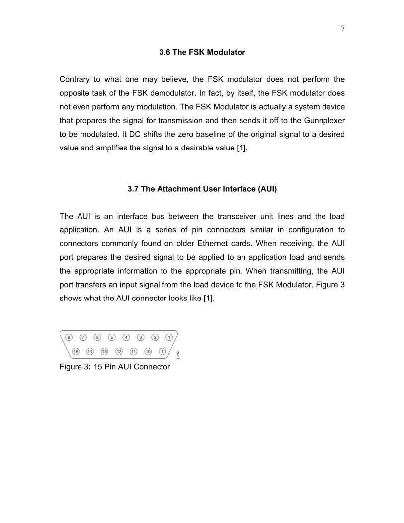
3.7 The Attachment User Interface (AUI) The AUI is an interface bus between the transceiver unit lines and the load
application. An AUI is a series of pin connectors similar in configuration to
connectors commonly found on older Ethernet cards. When receiving, the AUI
port prepares the desired signal to be applied to an application load and sends
the appropriate information to the appropriate pin. When transmitting, the AUI
port transfers an input signal from the load device to the FSK Modulator. Figure 3
shows what the AUI connector looks like [1].
Figure 3: 15 Pin AUI Connector
8
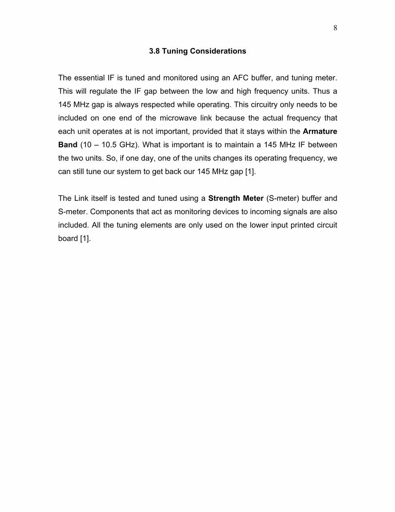
3.8 Tuning Considerations The essential IF is tuned and monitored using an AFC buffer, and tuning meter.
This will regulate the IF gap between the low and high frequency units. Thus a
145 MHz gap is always respected while operating. This circuitry only needs to be
included on one end of the microwave link because the actual frequency that
each unit operates at is not important, provided that it stays within the Armature Band (10 – 10.5 GHz). What is important is to maintain a 145 MHz IF between
the two units. So, if one day, one of the units changes its operating frequency, we
can still tune our system to get back our 145 MHz gap [1].
The Link itself is tested and tuned using a Strength Meter (S-meter) buffer and
S-meter. Components that act as monitoring devices to incoming signals are also
included. All the tuning elements are only used on the lower input printed circuit
board [1].
9
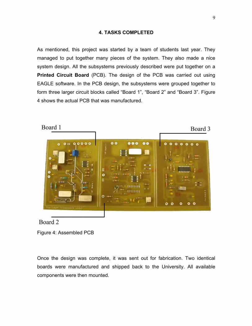
4. TASKS COMPLETED
As mentioned, this project was started by a team of students last year. They
managed to put together many pieces of the system. They also made a nice
system design. All the subsystems previously described were put together on a
Printed Circuit Board (PCB). The design of the PCB was carried out using
EAGLE software. In the PCB design, the subsystems were grouped together to
form three larger circuit blocks called “Board 1”, “Board 2” and “Board 3”. Figure
4 shows the actual PCB that was manufactured.
Figure 4: Assembled PCB
Once the design was complete, it was sent out for fabrication. Two identical
boards were manufactured and shipped back to the University. All available
components were then mounted.

10
4.1 Design of Subsystems
The following is a description of how the team designed each individual
subsystem, how they are interconnected and what components were used in the
design. The physical location of each subsystem is also discussed.
4.1.1 FSK Modulator
This FSK modulator, which sets up the signals to be modulated by the
Gunnplexer system at a carrier frequency in the 10 GHz band, is designed using
a Mini-Circuits PLP-21.4 low-pass filter, and a Burr-Brown OPA603 non-inverting
current feedback amplifier. A Mini-Circuits T2-1 balun transformer is also used to
better match the output of the low-pass filter to the AUI input. This circuit is
located on Board 1 of our PCB and is connected to the varactor diode terminal
input of the Gunnplexer through a 47Ω resistor [2].
4.1.2 Gunnplexer Assembly
The Gunnplexer assembly consists of a T4-1 Balun transformer, several resistors
and capacitors chosen to meet the necessary specifications, and the Gunnplexer
itself. Though currently, no Gunnplexer is connected to the circuitry, there are
terminals on the circuit board ready to connect to the three diodes of a
Gunnplexer. The Gunn diode terminal is connected directly to a terminal for bias
voltage which is in parallel with a 4.7µF Tantalum capacitor and a 0.1µF ceramic
capacitor. The Mixer diode terminal is connected to a T4-1 balun, which, on the
other side, is directly connected to the IF strip input. The varactor diode terminal,
as mentioned above connects directly to output of the FSK modulator circuitry.
This entire circuit is located on board 1 [2].
11
4.1.3 IF Strip The IF strip, which as we know, connects to the mixer diode input terminal after
having been matched with a balun, works at an operating frequency of 145 MHz.
The IF segment of the system has two jobs: filtering and amplification. The IF
strip is the third subsystem that has been integrated into the design of Board 1 of
the PCBs [2].
The filters used are a PHP-100 High Pass Filter and a PHP-200 Low Pass Filter
and the amplifiers used are MMIC MAR-6. Two such amplifiers are needed in the
IF strip. All components in the IF strip were used in compliance with the
specifications set forth by John Miles [2].
4.1.4 FSK Demodulator
Once the received signal has passed through the IF strip, it can then be
demodulated. The FSK demodulator is the subsystem that performs this task.
The FSK demodulator was designed using a Mini-Circuits MAR-4 operational
amplifier, a T4-1 balun and a Motorola MC13155 microchip and is located on
Board 2 of the PCBs [2].
4.1.5 Output Buffer The output buffer is connected to the output ports of the FSK demodulator on
one end, and to the input of the AUI port on the other end. It is designed using
four main components: two OPA603 amplifiers, a PLP-21.4 low-pass filter, and a
T1-1 balun transformer. The output buffer is located on Board 2 in conjunction
with the FSK demodulator [2].

12
4.1.6 The AFC Buffer The AFC Buffer is designed using a National Instruments LM324 operation
amplifier chip, which contains four identical op-amps, one of which is used to
monitor the differential output of the FSK demodulator. Another op-amp on the
same chip is used to connect to the tuning and fault meter. Though the AFC
buffer is only necessary at one end of the system, both PCBs have AFC buffer
circuits included on Board 3 [2].
4.1.7 The S-Meter Circuits
The S-meter buffer connects to the FSK demodulator at pin 12 of the MC-13155
chip. It uses one of the LM324 op-amps off the same chip as the AFC buffer. The
output of the S-meter buffer connects, through the S-meter circuitry to a panel
terminal. The panel terminal is meant to be connected to an S-meter display
panel. Like the AFC buffer, only one S-meter circuit is required, but S-meter
circuitry is located on Board 3 of both PCBs [2].
4.1.8 Tuning / Fault Meter The tuning and fault meter connects to the AFC buffer and to a pair of terminals,
across which a 0-100 µA current meter shall be placed. The tuning meter is the
last subsystem located on Board 3 of the PCBs [2].
13
4.2 Missing Elements Despite last year’s team having put much work into the design and
implementation of the overall system, there are still many missing pieces and
many aspects that have not been taken care of.
4.2.1 Missing Components
The PCBs are not complete. There are various resistors and capacitors that have
yet to be added to the circuit. The MC-13155 too was never added to the circuit.
The reason for this is because the chip did not arrive in time for last year’s team’s
deadline to submit the final report [2].
4.2.2 Incomplete Gunnplexer Assembly
Though the Gunnplexer system was designed and analyzed on paper, last year's
team did not ever actually set up the Gunnplexer module. That is to say, no
Gunnplexer was ever connected to the appropriate terminals of “Board 1”.
4.2.3 Meters and AUI ports
Thirdly, the tuning meters and S-meter displays have not been purchased, nor
has anything been set up to interface with the tuning circuits. Also, no AUI ports
were purchased or connected to the appropriate terminals of “Board 2”. As a result, of all this, the boards have actually never been tested and no
information is available that may or may not suggest that they will function
correctly.

14
4.3 Encountered Problems 4.3.1 Isolation of individual modules:
It was recommended by John Miles to have each subsystem in the overall design
enclosed individually. Doing so minimizes potential RF interference each
subsystem would have with every other subsystem. Unfortunately, as mentioned
earlier, the PCBs were designed to have three large circuit blocks each with
several subsystems integrated into them. Miles specifically points out that the IF
strip and the FSK demodulator are pieces that should be isolated. However, in
our design, the IF strip and the FSK modulator are integrated on the same
section of board and cannot be separated. Similarly The FSK demodulator is
attached to the output buffer, and it too cannot be separated. It is possible that
the system will still function correctly regardless. However, it is equally possible
that the system will not work as a result of interference.
4.3.2 Mismatch in Sizing of MC-13155 and PCB Socket
Since the final report was submitted last year, the MC-13155 microchips have
arrived. However, there is a mismatch between the sizing of the chip and the
sizing of the socket on the PCB where the chip is supposed to go. This mismatch
can be resolved using an Aries Electronics 35000X SOIC to DIP adapter.
However, using such an adapter may potentially lead to unwanted interference.

15
4.4 Clarification of Last Year’s Final Report Upon reviewing last year’s team’s final report, several things they had written
about were unclear. In this section, such issues will be clarified.
4.4.1 Inconsistency in Bandwidth Calculations In the final report, bandwidth is given as both 60 MHz and calculations are done
using 40 MHz. The bandwidth of 60 MHz was calculated using Carson's Rule for
FM bandwidth. However, the amplifier they are designing for is not in the
modulated FM band, rather, it is in the demodulated Ethernet band, which is
40MHz. Ultimately, this does not really matter because the op-amps used have a
BW of 160MHz. This is more than enough to accommodate the 40MHz that is
coming off the MC13155.
4.4.2 Use of Tantalum Capacitors
Our design seems to take a liking to tantalum capacitors. It found that, for this
application the electrolytic capacitors greater than 1 µF can be either aluminum
or tantalum. As a general rule of thumb, for capacitances greater than or equal to
1 µF, tantalum capacitors will be used. The MC-13155 chip also seems to like
tantalum bypass capacitors. It is most probably for this reason that certain
tantalum capacitors were originally used.

16
4.4.3 Disregarding Resistors
On p. 27 of the final report, we see that a 220 Ω resistor was neglected in
calculating the turn ratio of a balun. Doing this completely changes the values
obtained. It is true that the 220 Ω appears in parallel with 450 ohms for a total of
about 150 ohms. The 4:1 match to 50 ohms is just an approximation based on
two things: what Motorola shows in Figure 16 of the MC-13155 data sheet and
the fact that 4:1 is a more standard value for matching transformers than 3:1,
which would be a more appropriate transformer to use.
4.4.4 Connection of AUI ports For the application of out project we will have to connect two computers through
the AUI connector. To do this you cannot use a patch cable, a cable that
connects each pin to the same pin on the other end. A crossover cable must be
used. In the case of our project, the crossover cable would only have to connect
to 4 of the 15 pins as illustrated in the table below. The remaining pins are not
needed, but Pins 1, 8, 11 and 14 may have to be bonded together in order for the
network card to detect the presence of another card attached to it. Also it may
be possible that the network cards that we will use may require a few milliamps
of current be used from the +12V offered from pin 13. Since an AUI port has
separate pins for transmit and receive, it has the potential for full duplex,
although most applications will only use half-duplex. See Appendix A for more
information on how AUI ports work [6].
4.4.5 The Role of the TCP/IP and MAC Protocol in Error Correction For Ethernet connections, the protocol used is TCP/IP which accounts for certain
error correction. The TCP/IP protocol will continue with the regular error finding
that it supports. However because we are using an AUI connection, The
requirement for precision error detecting will be done by the AUI. Also The Full

17
duplex feature, which TCP allows, will not be used because of the half-duplex
nature of the signal received at the AUI port. As for the role the Media Access Control (MAC) protocol will have in this project, the initial scope John Miles set
forth was to create a Wireless MAC Ethernet Link. However the scope of our
project has been broadened to allow for any data communication, the MAC
protocol will only be necessary if our transmitted signal is Address Resolution
Protocol (ARP) from a host or Reverse Address Resolution Protocol from a guest
(RARP). ARP, and RARP are two of the techniques that occur in the location and
connection of 2 computers in a network environment under MAC protocol
conditions
4.4.6 Current Op-Amp Last year’s final report makes reference to a current op-amp. An op-amp in
general is a circuit element that performs certain signal processing applications.
Usually, it is used to increase the amplitude of an input voltage using external
voltage sources. However, a current op-amp does not exist. The correct
terminology is current feedback op-amp. In contrast with conventional op-amps,
the current feedback approach provides nearly constant bandwidth and settling
time over a wide range of closed loop voltage gains. The current op-amp fore
mentioned is simply a current feedback op-amp, which is a common active circuit
component.
4.4.7 OSI Model
In the final report, something called OSI is mentioned as being the network
model used in this project. OSI stands for Open System Interconnect. It is the
standard model for networking protocols and distributed applications. This model
was set forth by the International Standard Organization (ISO), and is commonly
called ISO / OSI. The model consists seven network layers, where each layer
carries information detailing how and where information is being transmitted
throughout the network.

18
4.4.8 How Inductance Arises in a PCB Parasitic inductors are formed across connections between layers of a PCB
called vias. The value of the inductance is a function of the diameter of the via
and the height, or spacing between layers. Combinations of vias that act like
inductors in series will cause inductance to increase. There are also trace-to
trace inductors that come about because the traces on a PCB are not infinitely
thin and nearby traces can cause inductive coupling.

19
5. TASKS AT HAND
This section outlines the work that must be done in order to get from where our
system currently stands to a working product. The first step is, of course, to
complete the circuit assembly. The next stage is the testing of all the individual
subsystems. A complete description on how to test these systems is included.
Beyond that, the remainder of the work will be to get the overall system to work
for a square wave input, for an Ethernet input and to explore other possible
applications of the system.
5.1 Completion of the Circuit Boards and Other Components
The first thing that must be done is the completion of the circuit boards started by
last year’s team. The most important addition to the PCBs is the mounting the
35000X adapter onto the circuit board and the mounting of the MC-13155 chip
onto the adapter. All the missing capacitors and resistors must also be mounted
on to the PCBs.
The S-Meter and the Tuning/Fault Meter also must be completed. The circuitry
needed for these meters has been included on “Board 3”. All that we must do is
attach a digital 200 mV panel meter to the S-Meter output terminal and a 100µA
analog current meter to its terminals to complete the tuning/fault meter system
[1].

20
5.2 Testing the Operation of the Circuit Boards 5.2.1 Gunnplexer Frequency Calibration
The first thing that must be done to get the 10 GHz link to work is tuning the
Gunnplexers. The Gunnplexers must be tuned to an appropriate frequency in
the Armature Band and must be set so that the frequencies of the two units are in
fact separated by 145 MHz. One thing that must be noted is that when the
supply voltage for the Gunn Diode is too low, the diode will heat up and possibly
get damaged.
Before connecting any supply voltage to the Gunnplexers, a bypass capacitor of
at least 0.1µF must be connected between the two terminals of the Gunn diodes.
Applying a +5V DC to the Gunnplexer varactor diode will establish the center IF
frequency. To keep power supply noise out of the system, the +5V should pass
through a 10 KΩ resistor followed by a 0.1µF bypass capacitor. In order to
accurately calculate the output frequency of the Gunnplexers, the output should
pass into a microwave frequency counter. To adjust the operating frequency of
the Gunnplexers we use its mechanical tuning screw. Turning the screw
clockwise will decrease the transmission frequency while turning it counter-
clockwise will increase the transmission frequency. The goal here is to set one
Gunnplexer to any chosen frequency and set the other to a frequency 145 MHz
higher or lower. In our case, we shall tune the lower of the two frequencies [1].
5.2.2 FSK Demodulator Calibration
In order for the MC13155 to operate in the appropriate frequency band, we must
choose an appropriate capacitor, inductor and resistor for the LC quadrature tank
circuit. John Miles specifies that he uses a home made inductor, a 22pF
capacitor and a 180 ohm resistor. The inductor was made of #22 enameled

21
copper wire wound three times around a screwdriver shaft to makes its shape. A
145 MHz sine wave as a source signal should be applied to the input of the
MC13155. An oscilloscope should be attached to pins 4 and 5 of the MC13155
to monitor the differential voltage between these two pins. By stretching and
compressing the coils of the inductor, we will change the differential voltage
between the two pins. The goal here is to achieve a differential voltage of about
10 to 20 mV. Once this is achieved the tank circuit is properly tuned and ready to
use with the demodulation circuit [1].
There is, theoretically, a more precise way to determine the requirements for the
components of the tank circuit. By following the equations given in the MC13155
datasheet, we can obtain values for our components. To determine the
necessary capacitance value, C, the documentation suggests using an external
capacitance of at least 20 pF. Since 22 pF is the closest value available, this is
what should be used. The MC13155 also has internal capacitance. This is in the
order of about 3 pF which results in a total capacitance of 25 pF for the tank
circuit. From this value, we can use equation (1) to calculate the needed
inductance.
( )2
2
21
cp fCL π= (1)
Where Cp= 25 pF and fc = IF = 145 MHz. Plugging these numbers into Equation
x. results in an inductance of 48nH. The closest standard inductor is 50nH.
We also know that for the Quadrature (Q):
BWf
Q c= (2)
We know that, in practice, the maximum bandwidth of any signal we will be using
is 40 MHz.

22
Therefore:
6.340
145==
MHzMHzQ
The total resistance value of the tank circuit is given by [3]:
( LfQR cT )π2= (3)
( )nHMHzRT 5014526.3 ××= π
Ω= 164TR
Knowing the internal resistance of the MC13155 is 3200Ω we can determine the
necessary resistor in our tank circuit using:
T
text RR
RRR
−=
int
int (4)
Ω−ΩΩΩ
=1643200164*3200
extR
Ω= 173extR
The closest standard value to resistance to this resistance is 180 ohms.
5.2.3 FSK Modulator Deviation Adjustment
This step is not all that critical since all it determines is the gain of the OPA603
amplifier. To conduct this adjustment, a 550-ohm variable potentiometer is set to
220-ohms and is used to set a gain of roughly 3.5 times the magnitude of the
input signal. At this point it is also a good idea to check and see if the amplified
waveform is similar to that of the input waveform to ensure proper transmission
[1].

23
5.2.4 Testing the IF Strip
To test the IF strip all we are looking for is the designed signal gain of 40 dB. To
do this we apply a signal of known amplitude at a frequency of 145 MHZ to the
input of the IF strip and attach a spectrum analyzer to its output. On the analyzer
we should be able to observe a 40 dB gain compared to that of the input signal
[1].
5.2.5 Testing Transceivers in Loop-Back Mode
It is possible to test the individual transceivers in what is known as loop-back
mode. Gunnplexers have a local echo characteristic, meaning the signal it sends
out is also received by itself. We can use this property to test modulation and
demodulation at the same time. We can simply apply an input 10MHz square
wave or sine wave signal to the input terminal of the transceiver. The output
terminal of the same transceiver should carry the same input signal. If this works
for multiple input signals, then the circuit should be working properly [1].

24
5.3 Testing the Entire System
After testing the individual subsystems of out circuit we will now have to test the
system as a whole. In other words, we must set up the system so that the two
Gunnplexer transceivers can communicate with one another. We test this by
connecting them to each other through an attenuated X-band waveguide. The
goal here is to be able to have a seamless connection between the two units
using the AUI interfaces as input and output terminals. We would like to be able
to transmit a signal at one end of the microwave link and receive the identical
signal at the other end of the link. This test must be performed in both directions
to ensure correct operation. We first perform this test using a 10 MHz square
wave as out input signal.
5.3.1 Ethernet Applications Once we get the system working, we can then replace the square wave input
with an Ethernet connection. For this setup, we will connect each of the units to a
computer system with AUI compatible network cards. This test is going to be
somewhat more involved, as there are factors that must be considered before
manipulating Ethernet signals. Nevertheless, if the link is working, the computers
should act as though they were connected directly to one another using the
appropriate crossover network cable.
5.3.2 Design of Antennas After we get the system working through a waveguide, we would like to actually
get the system to be wireless. We will design and use horn antennas to do this.
We will attach a horn antenna to each Gunnplexer and test the system for
operations over short distances. Once we get the link to work at close range, we
will move the two transceivers further apart to see what kind of range we can
achieve with this system.
25
5.4 Other Possible Applications of 10 GHz Link
Upon successful completion of a wireless Ethernet network, we will want to
explore other possible applications of this 10 GHz microwave system. A logical
extension to such a system would be to attempt to transmit an audio signal over
the link. If this is successful the next step after that would be to see if we can
transmit a video signal over the link. The goal in being able to send audio or
video signals over the link is to then be able to send both audio and video
simultaneously.
Since, as mentioned earlier, our system only operates in half-duplex we would
like to examine the possibility of converting it to full-duplex. This would allow us
to create an Ethernet connection that would not have any collisions, and hence,
better bandwidth. A major advantage of having a full-duplex system is that it
would allow us to have a wireless control system or maybe even allow high
bandwidth videoconferencing. Essentially, the possibilities are endless.

26
5.5 Summary and Breakdown of Tasks
5.5.1. Functionality of System The goal in this task is to go from what the system we currently have to a fully
operational communication link. It involves:
a. Completion of all circuitry
b. Testing the individual subsystems
c. Testing the overall system
5.5.2. Application of System to Ethernet Network This task consists of taking the functional microwave link and applying it to an
Ethernet application. This task includes:
a. Setup of functional computer network
b. Setup of AUI interface
c. Testing of network
5.5.3. Wireless Transmission The goal in this task is to successfully transmit a signal across a wireless
medium, and then improve the range of the system. Subtasks include:
a. Wireless link setup
b. Antenna Design
c. System Testing
5.5.4. Further Experimentation The last task should all else be working, is to put the finishing touches on the
system and experiment with other possible system applications.
a. System cosmetics
b. Experimentation with audio and video signals across the link
The following is a proposed timeline for completion of these tasks, as well as a
breakdown of who will be working on what.

27
Nov
embe
r 6, 2
002
Nov
embe
r 13,
200
2
Nov
embe
r 20,
200
2
Nov
embe
r 27,
200
2
Dec
embe
r 4, 2
002
Dec
embe
r 11,
200
2
Dec
embe
r 18,
200
2
Dec
embe
r 25,
200
2
Janu
ary
1, 2
003
Janu
ary
8, 2
003
Janu
ary
15, 2
003
Janu
ary
22, 2
003
Janu
ary
29, 2
003
Collin PhelpsCompletion of Circuit AssemblyTesting of SubsystemsAntenna Design
Nick TsaparasComputer ConfigurationTesting of SubsystemsSetup of AUI Interface
Michael BrownDesign Power Supply SystemConnection of Overall SystemAntenna DesignAntenna Testing
David LevineCompletion of Circuit AssemblyTesting of SubsystemsTesting Overall SystemWireless Link Setup
Mile
ston
es
Circ
uit C
ompl
eted
Circ
uit T
este
d
Phas
e 2
Rep
ort C
ompl
eted
Table 1: Task Allocation
28
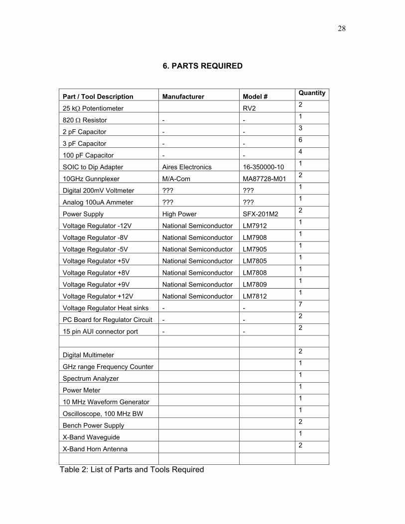
6. PARTS REQUIRED
Part / Tool Description Manufacturer Model # Quantity
25 kΩ Potentiometer RV2 2
820 Ω Resistor - - 1
2 pF Capacitor - - 3
3 pF Capacitor - - 6
100 pF Capacitor - - 4
SOIC to Dip Adapter Aires Electronics 16-350000-10 1
10GHz Gunnplexer M/A-Com MA87728-M01 2
Digital 200mV Voltmeter ??? ??? 1
Analog 100uA Ammeter ??? ??? 1
Power Supply High Power SFX-201M2 2
Voltage Regulator -12V National Semiconductor LM7912 1
Voltage Regulator -8V National Semiconductor LM7908 1
Voltage Regulator -5V National Semiconductor LM7905 1
Voltage Regulator +5V National Semiconductor LM7805 1
Voltage Regulator +8V National Semiconductor LM7808 1
Voltage Regulator +9V National Semiconductor LM7809 1
Voltage Regulator +12V National Semiconductor LM7812 1
Voltage Regulator Heat sinks - - 7
PC Board for Regulator Circuit - - 2
15 pin AUI connector port - - 2
Digital Multimeter 2
GHz range Frequency Counter 1
Spectrum Analyzer 1
Power Meter 1
10 MHz Waveform Generator 1
Oscilloscope, 100 MHz BW 1
Bench Power Supply 2
X-Band Waveguide 1
X-Band Horn Antenna 2
Table 2: List of Parts and Tools Required

29
7. CONCLUSION
To conclude this report, we can say that we are proceeding optimistically through
this project. We feel very strongly that we will be able to successfully set up a
working microwave link. We also understand that it is entirely possible that
various factors may set us back in trying to implement this system. Nevertheless,
we will take each challenge as it comes.
There is still much work to be done. We look forward to having much progress to
report at the end of Phase 2.

30
8. REFERENCES
[1] John Miles, “An Experimental 10-Mbits/s Microwave Data Link” http://www.qsl.net/ke5fx/uwave.html (current November, 2002)
[2] Benoît Chapelotte, Dave M. Gunputhram and Damien Avril, 10-GHz
Microwave Link, Tech. Report ELEC 490, Electrical and Computer Engineering Dept., Concordia University, Montreal, 2002
[3] Motorola, “MC13155 wideband FM IF subsystem IC”
http://www.qsl.net/ke5fx/uwave/mc13155.pdf (current November, 2002)
[4] B. P. Lathi, Modern Digital and Analog Communication Systems, Third Edition, Oxford University Press, 1998
[5] David M. Pozar, Microwave Engineering, Second Edition, John Wiley and
Sons Inc., New York, 1998 [6] Cisco Systems, “AUI Technical Specifications”
http://www.cisco.com/univercd/cc/td/doc/product/lan/14201220/14_1220u/csspec.htm, (current November 2002)

31
APPENDIX A: HOW THE AUI CONNECTOR WORKS The following tables detail the connection made to an AUI port, and the relevant
ports to ensure proper transmission when connecting two PC Ethernet card
together.
Pin Label Description 1 GND Ground 2 CI+ Positive AUI differential collision-data input 3 TX+ Positive AUI differential transmit-data input 4 GND Ground 5 RX+ Positive AUI differential receive-data output 6 GND Ground 7 NC 8 GND Ground 9 CI- Negative AUI differential collision data 10 TX- Negative AUI differential transmit-data input 11 GND Ground 12 RX- Negative AUI differential receive-data output 13 +12V 12V supply for external MAU 14 GND Ground 15 NC Table 3: AUI pin connections PC A PC B Pin 3 Pin 5 Pin 5 Pin 3 Pin 10 Pin 12 Pin 12 Pin 10
Table 4: Connection Between Two PC Ethernet Cards