10 chapter 4.pdf
TRANSCRIPT
66
CHAPTER 4
HARDWARE IMPLEMENTATION OF 60W MODULE USING
MICROCONTROLLER
The concept of maximum power point tracking in solar photovoltaic cells is
demonstrated by a basic model consisting of a photovoltaic module, a buck converter
and resistive load. The control signals required for the hardware implementation are
generated from a microcontroller circuit.
4.1 COMPONENTS USED FOR IMPLEMENTATION 4.1.1 Photovoltaic Module A 60W solar photovoltaic module from P6 series of KL solar company having 36
crystalline silicon solar cells is used for experimentation. The 36 cells in series
provide 60W of maximum power. The electrical specifications of the module are as
follows:
Maximum power --- 60W
Open circuit voltage --- 21V
Short Circuit Current --- 3.74A
Maximum power point voltage --- 17.1V
Maximum power point current --- 3.5A
4.1.2 FGA25N120ANTD The Fairchild FGA25N120ANTD is a 1200V non –punch through trench
insulated – gate bipolar transistor device. Using Fairchild's proprietary trench design
and advanced NPT technology, the 1200V NPT IGBT offers superior conduction and
switching performances, high avalanche ruggedness and easy parallel operation. It has
67
the features of positive temperature coefficient, low saturation voltage, low switching
loss and extremely enhanced avalanche capability.
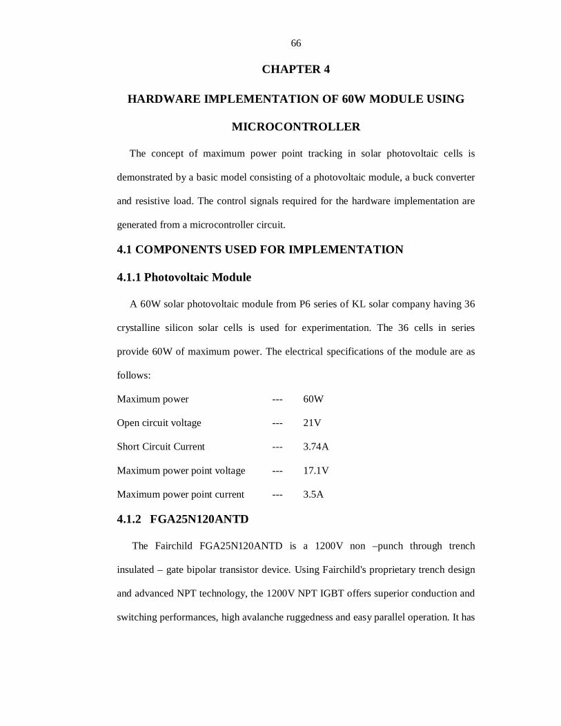
4.1.3 HCPL 3120
Fig: 4.1 HCPL 3120 connection diagram The HCPL-3120 gate drive optocouplers contain a GaAsP LED. The LED is
optically coupled to an integrated circuit with a power output stage. It is ideally suited
for driving power IGBTs and MOSFETs. The high operating voltage range of the
output stage provides the drive voltages required by gate controlled devices. The
voltage and current supplied make it ideally suited for directly driving IGBTs with
ratings up to 1200 V/100 A. For IGBTs with higher ratings, the HCPL-3120 series is
used to drive a discrete power stage which drives the IGBT gate. It has the features of
0-5V maximum low level output voltage which eliminates need for negative gate
drive, under voltage lockout protection with hysteresis, wide operating Vcc range of
15 to 30V and 500ns maximum switching speeds.
4.1.4 7805
The voltage source in a circuit will have fluctuations and would not give the fixed
voltage output. The 78xx family is commonly used in electronic circuits requiring a

68
regulated power supply due to their ease-of-use and low cost. For ICs within the
family, the xx is replaced with two digits, indicating the output voltage. The 78xx line
are positive voltage regulators. They produce a voltage that is positive relative to a
common ground. 78xx ICs have three terminals and support an input voltage
anywhere from a couple of volts over the intended output voltage, up to a maximum
of 35 or 40 volts, and typically provide 1 or 1.5 amperes of current. With proper heat
sink these 78xx types can handle even more than 1A current. They also have thermal
overload protection, short circuit protection.
7805 provides +5V regulated power supply. Capacitors of suitable values are
connected at input and output pins depending upon the respective voltage levels.
Fig: 4.2 Pin out diagram of 7805 The 7805 has three leads. If 7805 is looked from the front, the three leads are, from
left to right, input voltage, ground and output voltage. The first capacitor takes out
any ripple coming from the transformer so that the 7805 is receiving a smooth input
voltage and the second capacitor acts as a load balancer to ensure consistent output
from 7805. The advantages are that the 78xx series ICs do not require additional
components to provide a constant, regulated source of power, making them easy to
use, as well as economical and efficient usage of space. 78xx series ICs have built-in
protection against a circuit drawing too much power. They have protection against
overheating and short-circuits, making them quite robust in most applications.

69
The disadvantages are that the input voltage must always be higher than the output
voltage by some minimum amount which makes these devices unsuitable for
powering some devices from certain types of power sources. For some applications an
adequate heat sink is provided.
4.1.5 Diode IN4007 IN4007 diode used for rectification has maximum reverse bias voltage capacity of
50V and maximum forward current capacity of 1A.
4.1.6 30EPF06 30EPF06 rectifier series is optimised for combined short reverse recovery time of
60ns and low forward voltage drop of less than 1.2V at 10A. The 30EPF06 rectifier
series is used for output rectification and free wheeling in inverters, choppers and
converters. This rectifier series is also used for input rectifications where severe
restrictions on conducted EMI should be met.
4.1.7 In System Programming Header
In System Programming is the ability of some programmable logic devices,
microcontrollers and other programmable electronic chips to be programmed while
installed in a complete system, rather than requiring the chip to be programmed prior
to installing it into the system. This allow manufacturers to program their chips in
their own system’s production line instead of buying pre programmed chips from a
manufacturer, making it feasible to apply code or design changes in the middle of a
production run.
An 'ISP Header' is the connector used to interface the cable which carries the
programming signals from an external ISP Programmer to the Target System Circuit
Board / Microcontroller. The programming signals are routed via the ISP Header to
the Target Device on the Target System Circuit Board.
70
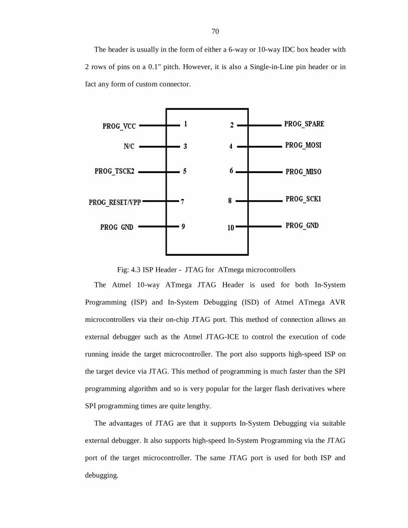
The header is usually in the form of either a 6-way or 10-way IDC box header with
2 rows of pins on a 0.1" pitch. However, it is also a Single-in-Line pin header or in
fact any form of custom connector.
Fig: 4.3 ISP Header - JTAG for ATmega microcontrollers The Atmel 10-way ATmega JTAG Header is used for both In-System
Programming (ISP) and In-System Debugging (ISD) of Atmel ATmega AVR
microcontrollers via their on-chip JTAG port. This method of connection allows an
external debugger such as the Atmel JTAG-ICE to control the execution of code
running inside the target microcontroller. The port also supports high-speed ISP on
the target device via JTAG. This method of programming is much faster than the SPI
programming algorithm and so is very popular for the larger flash derivatives where
SPI programming times are quite lengthy.
The advantages of JTAG are that it supports In-System Debugging via suitable
external debugger. It also supports high-speed In-System Programming via the JTAG
port of the target microcontroller. The same JTAG port is used for both ISP and
debugging.

71
4.1.8 ATmega8L
A microcontroller is a small computer on a single integrated circuit consisting of a
relatively simple CPU combined with serial input output such as serial ports, other
serial communications interfaces like serial peripheral interface, controller area
network for system interconnect peripherals such as timers, event counters, PWM
generators, watch dog, volatile memory for data storage, RM, EPROM, EEPROM for
program and operating parameter storage, clock generator – often an oscillator for a
quartz timing crystal, resonator. This integration drastically reduces the number of
chips and the amount of wiring and the circuit board space that is needed to produce
equivalent systems using separate chips. Further more, each pin is in interface to
several internal peripherals, with the pin function selected by software. A
microcontroller instruction set usually has many instructions intended for bit-wise
operations to make control programs more compact.
The microcontroller used is AVR microcontroller – ATmega8L.
The ATmega8L is a low-power CMOS 8-bit microcontroller based on the AVR
RISC architecture. By executing powerful instructions in a single clock cycle, the
ATmega8L achieves throughputs approaching 1 MIPS per MHz, allowing the system
designer to optimize power consumption versus processing speed. The AVR core
combines a rich instruction set with 32 general purpose working registers. All the 32
registers are directly connected to the Arithmetic Logic Unit (ALU), allowing two
independent registers to be accessed in one single instruction executed in one clock
cycle. It has 8K bytes of In-System Programmable Flash with Read-While-Write
capabilities, 512 bytes of EEPROM, 1K byte of SRAM, 23 general purpose I/O lines,
32 general purpose working registers, three flexible Timer/Counters with compare
modes, internal and external interrupts, a serial programmable USART, a byte

72
oriented Two-wire Serial Interface, a 6-channel ADC with 10-bit accuracy, a
programmable Watchdog Timer with Internal Oscillator, an SPI serial port, and five
software selectable power saving modes.
4.1.9 AVR Studio
It is an Integrated Development Environment for writing and debugging AVR
applications in Windows 98/XP/ME/2000 and Windows NT environments. AVR
Studio provides a project management tool, source file editor and chip simulator. It
also interfaces with In-Circuit Emulators and development boards available for the
AVR 8-bit RISC family of microcontrollers.
It has got the following simplifying development tasks.
Integrated development environment for writing, compiling and debugging
software
Fully symbolic source-level debugger
Configurable memory views, including SRAM, EEPROM, Flash, Registers,
and I/Os
Unlimited number of break points
Trace buffer and trigger control
Online HTML help
Variable watch/edit window with drag-and-drop function
Extensive program flow control options
Simulator port activity logging and pin input stimuli
Support for C, Pascal, BASIC and assembly languages
4.1.10 Buck Converter
Buck, boost and buck-boost are three basic circuit families used in switching
regulated power supplies. These three circuit topologies are operated in one of the two

73
modes: The discontinuous or continuous current modes. The choice of operational
mode has great effect on the operational characteristics. Each of the three basic circuit
families has a unique set of relationships between input and output voltages, currents
and duty cycle. The basic buck regulator functions only with the output voltage less
than input voltage and with the same polarity. The boost circuit requires the output
voltage greater than input voltage. The flyback topology functions with output voltage
either less than or greater than the input voltage, but the polarity must be opposite.
The three different switching circuits employ the same three elements (inductor,
transistor and diode), but arranged in a different manner. The output capacitors are
filter elements.
Transistors chosen for use in switching power supplies must have fast switching
times and should be able to withstand the voltage spikes produced by the inductor.
An inductor is used in a filter to reduce the ripple in current. This reduction occurs
because current through the inductor cannot change suddenly. When the current
through an inductor tends to fall, the inductor tends to maintain the current by acting
as a source. Inductors used in switched supplies are usually wound on toroidal cores,
often made of ferrite or powdered iron core with distributed air-gap to minimize core
losses at high frequencies.
A capacitor is used in a filter to reduce ripple in voltage. Since switched power
regulators are usually used in high current, high-performance power supplies, the
capacitor is chosen for minimum loss. Loss in a capacitor occurs because of its
internal series resistance and inductance. Capacitors for switched regulators are
chosen on the basis of effective series resistance. Solid tantalum capacitors are the
best in this respect. For very high performance power supplies, sometimes it is
necessary to parallel capacitors to get a low enough effective series resistance.

74
The diode used in a switched regulator is usually referred to as free-wheeling
diode or a catch diode. The purpose of this diode is not to rectify, but to direct current
flow in the circuit and to ensure that there is always a path for the current to flow into
the inductor. It is also necessary that this diode should be able to turn off relatively
fast. Diodes known as the fast recovery diodes are used in these applications.
Most of the switched supplies need a minimum load, in order to ensure that the
inductor carries current always. If the current flow through the inductor is not
continuous, regulation becomes poor.
The buck converter can be controlled in two ways, known as:
Constant-frequency operation or pulse-width modulation control
Variable-frequency operation or control by frequency modulation
With pulse-width modulation control, the regulation of output voltage is achieved
by varying the duty cycle of the switch, keeping the frequency of operation constant.
Duty cycle refers to the ratio of the period for which the power semiconductor is kept
ON to the cycle period. Usually control by pulse width modulation is the preferred
method since constant frequency operation leads to optimization of LC filter and the
ripple content in output voltage is controlled within the set limits. On the other hand,
if the load on the converter is below a certain level, voltage regulation of output
becomes a problem and in such a case, control by frequency modulation is to be
preferred. When control by frequency modulation is to be achieved, the ON period of
the power semiconductor switch is kept constant and the frequency of operation is
varied to effect voltage regulation. Design of LC filter is not easy in such a case.
If a micro-controller is used instead of a specific PWM IC, it is possible to switch
from one mode of control to the other depending on the load conditions.
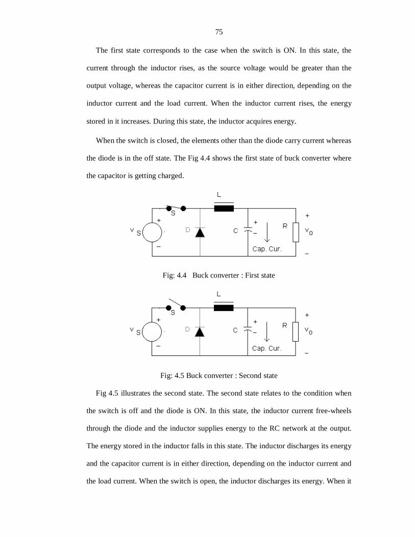
The buck converter circuit can operate in any of the three states as explained below:
75
The first state corresponds to the case when the switch is ON. In this state, the
current through the inductor rises, as the source voltage would be greater than the
output voltage, whereas the capacitor current is in either direction, depending on the
inductor current and the load current. When the inductor current rises, the energy
stored in it increases. During this state, the inductor acquires energy.
When the switch is closed, the elements other than the diode carry current whereas
the diode is in the off state. The Fig 4.4 shows the first state of buck converter where
the capacitor is getting charged.
Fig: 4.4 Buck converter : First state
Fig: 4.5 Buck converter : Second state
Fig 4.5 illustrates the second state. The second state relates to the condition when
the switch is off and the diode is ON. In this state, the inductor current free-wheels
through the diode and the inductor supplies energy to the RC network at the output.
The energy stored in the inductor falls in this state. The inductor discharges its energy
and the capacitor current is in either direction, depending on the inductor current and
the load current. When the switch is open, the inductor discharges its energy. When it
76
has discharged all its energy, its current falls to zero and tends to reverse, but the
diode blocks conduction in the reverse direction.
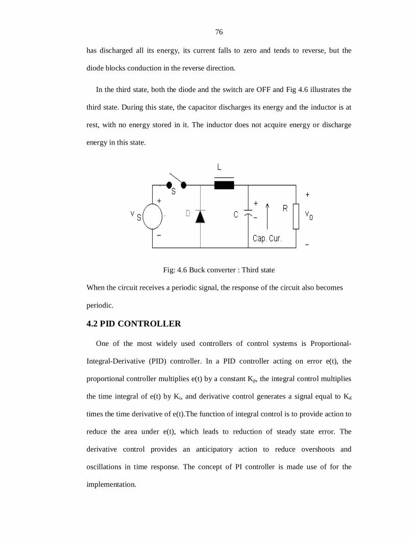
In the third state, both the diode and the switch are OFF and Fig 4.6 illustrates the
third state. During this state, the capacitor discharges its energy and the inductor is at
rest, with no energy stored in it. The inductor does not acquire energy or discharge
energy in this state.
Fig: 4.6 Buck converter : Third state
When the circuit receives a periodic signal, the response of the circuit also becomes
periodic.
4.2 PID CONTROLLER
One of the most widely used controllers of control systems is Proportional-
Integral-Derivative (PID) controller. In a PID controller acting on error e(t), the
proportional controller multiplies e(t) by a constant Kp, the integral control multiplies
the time integral of e(t) by Ki, and derivative control generates a signal equal to Kd
times the time derivative of e(t).The function of integral control is to provide action to
reduce the area under e(t), which leads to reduction of steady state error. The
derivative control provides an anticipatory action to reduce overshoots and
oscillations in time response. The concept of PI controller is made use of for the
implementation.
77
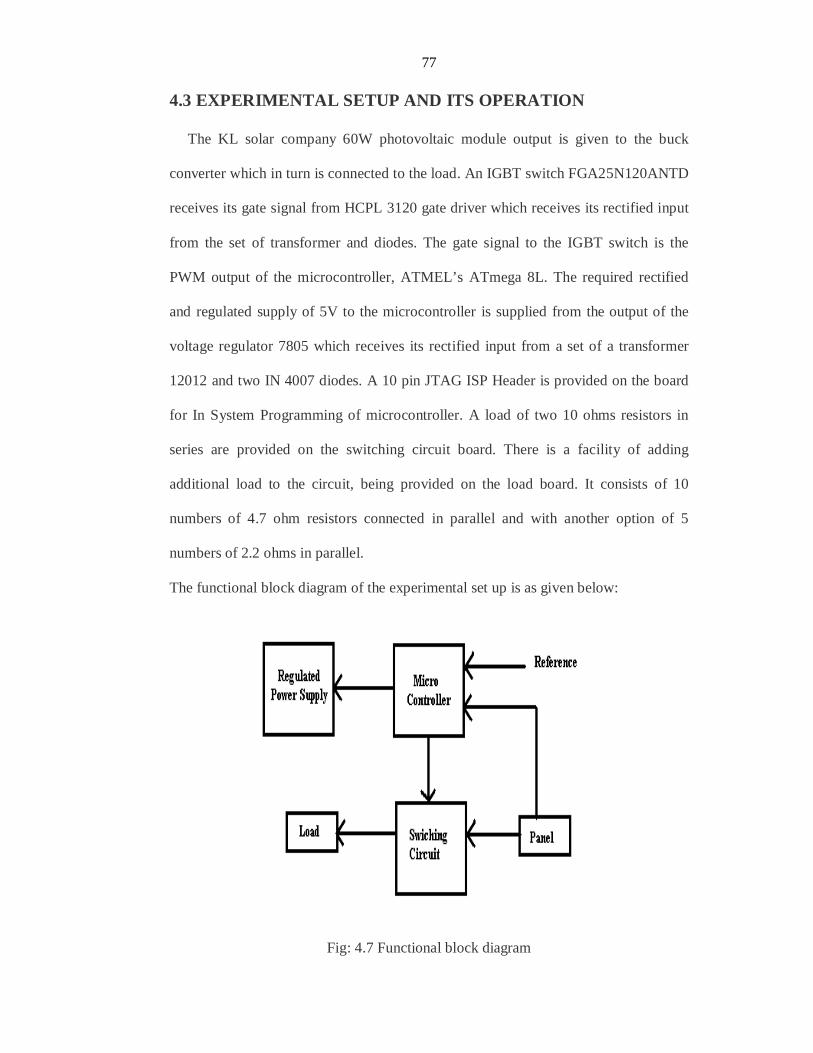
4.3 EXPERIMENTAL SETUP AND ITS OPERATION
The KL solar company 60W photovoltaic module output is given to the buck
converter which in turn is connected to the load. An IGBT switch FGA25N120ANTD
receives its gate signal from HCPL 3120 gate driver which receives its rectified input
from the set of transformer and diodes. The gate signal to the IGBT switch is the
PWM output of the microcontroller, ATMEL’s ATmega 8L. The required rectified
and regulated supply of 5V to the microcontroller is supplied from the output of the
voltage regulator 7805 which receives its rectified input from a set of a transformer
12012 and two IN 4007 diodes. A 10 pin JTAG ISP Header is provided on the board
for In System Programming of microcontroller. A load of two 10 ohms resistors in
series are provided on the switching circuit board. There is a facility of adding
additional load to the circuit, being provided on the load board. It consists of 10
numbers of 4.7 ohm resistors connected in parallel and with another option of 5
numbers of 2.2 ohms in parallel.
The functional block diagram of the experimental set up is as given below:
Fig: 4.7 Functional block diagram

78
The connection circuit diagram is shown below:
Fig: 4.8 Circuit diagram
Experimental set up of the switching circuit board, controller circuit board and the
load board are shown below in the Fig 4.9, 4.10 and 4.11 respectively.

79
Fig: 4.9 Experimental set up of switching circuit
Fig: 4.10 Experimental set up of controller circuit
80
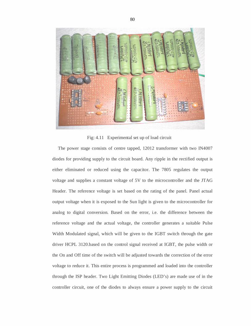
Fig: 4.11 Experimental set up of load circuit
The power stage consists of centre tapped, 12012 transformer with two IN4007
diodes for providing supply to the circuit board. Any ripple in the rectified output is
either eliminated or reduced using the capacitor. The 7805 regulates the output
voltage and supplies a constant voltage of 5V to the microcontroller and the JTAG
Header. The reference voltage is set based on the rating of the panel. Panel actual
output voltage when it is exposed to the Sun light is given to the microcontroller for
analog to digital conversion. Based on the error, i.e. the difference between the
reference voltage and the actual voltage, the controller generates a suitable Pulse
Width Modulated signal, which will be given to the IGBT switch through the gate
driver HCPL 3120.based on the control signal received at IGBT, the pulse width or
the On and Off time of the switch will be adjusted towards the correction of the error
voltage to reduce it. This entire process is programmed and loaded into the controller
through the ISP header. Two Light Emitting Diodes (LED’s) are made use of in the
controller circuit, one of the diodes to always ensure a power supply to the circuit

81
board and the other to ensure correct program running status of microcontroller. Pots
are used to give the input error voltage scaled to the compatible values.
In microcontroller, the double buffered Output Compare Register (OCR1A) is
compared with the Timer/Counter value at all time. The result of the compare is used
by the waveform generator to generate a PWM or variable frequency output on the
Output Compare pin (OC1A). The TOP value, or maximum Timer/Counter value, is
in some modes of operation be defined by either the OCR1A register, the ICR1
register, or by a set of fixed values.
The ICR1 register is written when using a waveform generation mode that utilizes
the ICR1 register for defining the counter’s TOP value. In these cases the waveform
generation mode bits must be set before the TOP value can be written to the ICR1
register.
The 16-bit comparator continuously compares TCNT1 with the Output Compare
Register (OCR1A). If TCNT equals OCR1A, the comparator signals a match. A
match will set the Output Compare Flag (OCF1A) at the next timer clock cycle. The
waveform generator uses the match signal to generate an output according to operating
mode set by the waveform generation mode bits and compare output mode bits.
The ATmega8L features a 10-bit successive approximation ADC. The ADC is
connected to an 8-channel analog multiplexer which allows eight single-ended voltage
inputs constructed from the pins of Port C. The single-ended voltage inputs refer to
0V. The ADC contains a Sample and Hold circuit which ensures that the input voltage
to the ADC is held at a constant level during conversion. Internal reference voltages of
nominally 2.56V or AVCC are provided On-chip. The voltage reference is externally
decoupled at the AREF pin by a capacitor for better noise performance.
The ADC converts an analog input voltage to a 10-bit digital value through

82
successive approximation. The minimum value represents GND and the maximum value
represents the voltage on the AREF pin minus 1 LSB. Optionally, AVCC or an internal
2.56V reference voltage may be connected to the AREF pin by writing to the
REFSn bits in the ADMUX Register. The internal voltage reference is decoupled by an
external capacitor at the AREF pin to improve noise immunity. The analog input
channel is selected by writing to the MUX bits in ADMUX. Any of the ADC input
pins, as well as GND and a fixed band gap voltage reference, can be selected as single
ended inputs to the ADC. The ADC is enabled by setting the ADC Enable bit, ADEN
in ADCSRA. Voltage reference and input channel selections will not go into effect until
ADEN is set. The ADC generates a 10-bit result which is presented in the ADC
data registers, ADCH and ADCL. By default, the result is presented right adjusted,
but can optionally be presented left adjusted by setting the ADLAR bit in ADMUX.
A single conversion is started by writing a logical one to the ADC start conversion
bit, ADSC. This bit stays high as long as the conversion is in progress and is cleared by
hardware when the conversion is completed.
In free running mode, the ADC is constantly sampling and updating the ADC
data register. Free running mode is selected by writing the ADFR bit in ADCSRA
to one. The first conversion must be started by writing a logical one to the ADSC
bit in ADC-SRA. In this mode the ADC will perform successive conversions
independently of whether the ADC interrupt flag, ADIF is cleared or not. The
reference voltage for the ADC (VREF) indicates the conversion range for the ADC.
Keeping in view the above points regarding the operation of the microcontroller
whose processor speed is 8 MHz, the initialization of the ports and the registers are
done. Ports B and D are set as output ports and the port C is selected as input port. The
timer1 is set to fast PWM mode and hence TCCR1A is initialized to OXBE, TCCR1B

83
to 0x19. ICR1 is set to TOP for a switching frequency of 10 KHz. OCR1A is initialized
for 50% PWM duty cycle and ADMUX is set for internal 5V reference value.
Following are the steps involved in order in the operation of the circuit:
(a) Initialise ports, PWM and ADC modules
(b) Read previous value and the current value
(c) Calculate error
(d) Calculate PI
(e) Update PWM
(f) Go to step (c)
Calculation of PI involves the following steps:
(a) Read ADC channel 0 value and set it as set_value.
(b) Read ADC channel 1 value and set it as actual_value
(c) Initialize pre_er[4] to zeroes
(d) Define Kp, Ki values
(e) er_1 = set_value – actual_value
(f) pout = Kp * er_1
(g) iout = (pre_er[0] + pre_er[1] + pre_er[2] + pre_er[3] + er_1) * Ki
(h) latest_value = pout + iout
(i) Update pre_er[4] values
(j) Go to step (e)

84
4.4 RESULTS
The following are the measurements of voltages and currents taken at different
times in a day with and without maximum power point tracking.
Table 4.1: Measurements with and without MPPT
The results show that for a given load, by employing MPPT concept, the voltage at
maximum power point is achieved and hence the power output from the cell is
enhanced or maximized.
4.5 CONCLUSIONS
It can be concluded that the use of maximum power point tracking concept
significantly enhances the power output from the cell. The observations at various
timings in a day for a 60 W module using Atmega 8L microcontroller are presented
and the results show the improvement in the power output with the presaence of
maximum power point tracker.
Without MPPT With MPPT Time V(V) I(A) P(W) V(V) I(A) P(W) 9 am 6 0.54 3.24 17 0.9 15.3 11am 10 1.2 12 17 2 34 1 pm 15 2.4 36 17 3.2 54.4 3 pm 11 1.9 20.9 17 2.2 37.4 5 pm 5 0.5 2.5 17 1 17